1
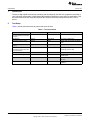
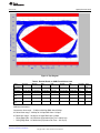
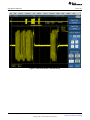
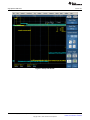
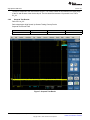
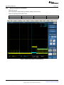
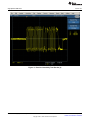
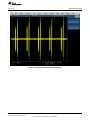
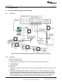
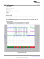
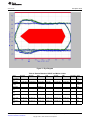
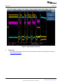
Application Report
SPRABU3 – April 2014
Validating High- and Full-Speed USB on TMS320C5517
ABSTRACT
This application report describes the process to validate electrical requirements of high- and full-speed
USB operations on the TMS320C5517 device.
1
2
3
4
5
Contents
Introduction ................................................................................................................... 2
Test Setup .................................................................................................................... 2
High-Speed USB Tests ..................................................................................................... 5
Full-Speed Tests ........................................................................................................... 24
References .................................................................................................................. 28
List of Figures
1
Test Setup .................................................................................................................... 3
2
Waveform Plot................................................................................................................ 6
3
Eye Diagram .................................................................................................................. 7
4
Packet Parameter Test Results (a) ........................................................................................ 9
5
Packet Parameter Test Results (b) ...................................................................................... 10
6
Chirp Test Result ........................................................................................................... 12
7
Suspend Test Result ....................................................................................................... 14
8
Resume Test Result ....................................................................................................... 15
9
Reset from Suspend Test Results (a) ................................................................................... 16
10
Reset from Suspend Test Results (b) ................................................................................... 17
11
Receiver-Sensitivity Test Results (a) .................................................................................... 22
12
Receiver-Sensitivity Test Results (b) .................................................................................... 23
13
Device and Hub Upstream Signaling Test and Receiver Test Schematic .......................................... 24
14
Waveform Plot .............................................................................................................. 26
15
Eye Diagram ................................................................................................................ 27
16
Signal Quality Test Results ............................................................................................... 28
List of Tables
1
Test Instruments ............................................................................................................. 2
2
Power Supply Voltages ..................................................................................................... 4
3
Results Based on USB-IF and Waiver Limit
4
Results Based on USB-IF and Waiver Limits
SPRABU3 – April 2014
Submit Documentation Feedback
............................................................................. 7
.......................................................................... 27
Validating High- and Full-Speed USB on TMS320C5517
Copyright © 2014, Texas Instruments Incorporated
1
Introduction
1
www.ti.com
Introduction
The device high-speed electrical test procedure was developed by the USB 2.0 compliance committee to
verify electrical requirements of high-speed USB operations designed to meet USB 2.0 specification. This
document outlines the test setup and captures the results of the series tests performed on the C5517
device.
2
Test Setup
Table 1 lists the test instruments to perform the series of tests.
Table 1. Test Instruments
2
Type
Manufacturer
Product
Use
USB high-speed electrical test
tool to be loaded on a test bed
computer
USB-IF
USBHSET
To enumerate and send command
Oscilloscope
Tektronix
CSA 8000B
To measure USB signals
Differential probe (1 probe)
Tektronix
P6247
Signal quality and receiver sensitivity
tests
Single-ended FET probe (2
probes)
Tektronix
P6245
Packet parameters and CHIRP timings
Measurement application (USB Tektronix
test software that is part of the
scope application)
TDSUSB
USB compliance test software
specifically used for USB
Test fixture
Tektronix
TDSUSBF
For USB test
Arbitrary waveform generator
Tektronix
AWG7102
To generate serial test data for receiver
sensitivity test
Digital Multi-meter
Fluke
Fluke 45 Series
Measure voltage and current DP and
DM lines
Test board
TI and Spectrum Digital
EVM
Test board used for C5517 USB
validation
Validating High- and Full-Speed USB on TMS320C5517
Copyright © 2014, Texas Instruments Incorporated
SPRABU3 – April 2014
Submit Documentation Feedback
Test Setup
www.ti.com
2.1
Test Fixture
Figure 1 provides the setup for validating tests.
Test Setup
Droop Test Load
Key
Test name/connector
Switch function
A
A-Dongle connector
A
A-Receptacle
B
B-Receptacle
J4
J1
J3
J2
Switches S4, S3, S51 and S61, set
load current on loads 2, 4, 6, and 8.
Switches S1, S2, S81 and S71, set
load current on loads 1, 3, 5, and 7.
J81
J150
J71
J61
J70
A
J72
LS/FS Downstream
Signal Quality (Device)
J10
Inrush Current, LS/FS
Upstream Signal Quality
Inrush Current Test State:
Discharge, Off, On.
J7
A
A
Inrush Current
Probe Test Loop
J12
A
A
J16
High-speed Host Signal Quality
J14
J20
Adjacent Trigger and Droop
High-speed Host TDR
A
A
A - receptacle on the back of the board
J19
A
High-speed Device TDR
J26
A - receptacle on the back of the board
J28
A
A - receptacle on the back of the board
J32
High-speed through connection
for packet parameter, suspend,
resume and reset.
J34
High-speed Receiver
Sensitivity
Signal Quality - HS Upstream
A
J37
High-speed Device Signal
Quality Connection
Init LED
S6 - Init /Test Switch
J91 J35
Jumper for power selection (USB Vbus or user supplied 5V)
J92
DC Power in Jack
Figure 1. Test Setup
SPRABU3 – April 2014
Submit Documentation Feedback
Validating High- and Full-Speed USB on TMS320C5517
Copyright © 2014, Texas Instruments Incorporated
3
Test Setup
2.2
www.ti.com
Setup for High-Speed USB Tests
2.2.1
Test Condition
2.2.1.1
Power Supply Voltage and Temperature
Table 2 shows the power supply voltage.
Table 2. Power Supply Voltages
Parameter
2.2.1.2
Min
Typ
Max
Unit
USB_VDD1P3
Supply voltage, Digital USB
1.24
1.3
1.43
V
USB_VDDA1P3
Supply voltage, 1.3-V Analog USB
1.24
1.3
1.43
V
USB_VDDA3P3
Supply voltage, I/O, 3.3-V Analog USB PHY
2.97
3.3
3.63
V
Test Items
The following tests used the voltage supplies in Table 2.
Test Number
Test Items
Result
USB_EL_2
HS Transmitter data rate 480 Mb/s ± 0.05%
PASSED
USB_EL_4
Signal quality test measured at the near end
PASSED
USB_EL_6
10% to 90% differential rise and fall time > 500ps
PASSED
USB_EL_7
Monotonic data transitions over the vertical openings in the
appropriate EYE Pattern
PASSED
High Speed Signal Quality Test
Device Packet Parameters
USB_EL_21
Synchronization (SYNC) field
PASSED
USB_EL_22
Inter-packet gap (delay between Host and device packet)
PASSED
USB_EL_25
End of packet (EOP) field
PASSED
USB_EL_28
Chirp reset time
PASSED
USB_EL_29
Chirp-K duration
PASSED
USB_EL_31
Delay between last Host chirp and device disconnect 1.5 K pullup resistor and enable termination
PASSED
USB_EL_27
Chirp handshake generation while Host performing reset in the
middle of idle (non-suspend HS mode)
PASSED
USB_EL_28
Chirp-K duration when reset is invoked from a suspended state
PASSED
USB_EL_38
Chirp reset time when reset is applied from a suspend state
PASSED
USB_EL_39
Device support for suspend state
PASSED
USB_EL_40
Device transition from suspend state to HS operation due to
reaching the EOF
PASSED
Chirp Timings
Device Suspend, Resume, and Reset Timing
Device Test J/K, SE0_NAK
USB_EL_8
Test J/K (controller transmits continuous J)
PASSED
USB_EL_8
Test K (controller transmits continuous K)
PASSED
USB_EL_9
Test_SE0_NAK (controller responds to any valid IN token with a
NAK)
PASSED
USB_EL_16
Device receiver level
PASSED
USB_EL_17
Device squelch level
PASSED
USB_EL_18
Device capability for locking PLL with 12-bit SYNC field
PASSED
Device Receiver Sensitivity
4
Validating High- and Full-Speed USB on TMS320C5517
Copyright © 2014, Texas Instruments Incorporated
SPRABU3 – April 2014
Submit Documentation Feedback
High-Speed USB Tests
www.ti.com
3
High-Speed USB Tests
3.1
Device High-Speed Signal Quality (EL_2/4/5/6/7)
3.1.1
Procedure
NOTE: Use care to determine if the device under test incorporates a captive cable or has a normal
series B or mini-B receptacle. Captive cable designs require the signal quality measurement
to be made at the far end (hsfe). Detachable cable designs require the measurement to be
made at the near end (hsne).
1.
2.
3.
4.
5.
Turn on the oscilloscope and allow 20 minutes for warm up.
Launch the TDSUSB software application on the oscilloscopes.
Press the Default Setup button on the oscilloscope front panel.
In the applications menu bar, select File → Recall default.
Within the Measurement select menu of the USB2.0 compliance test application, select the High
Speed tab.
6. Within the Signal Quality area of the application, select the High Speed Signal Quality tests → Eye
Diagram, Signal Rate, Rise time, Fall Time, and EOP Width.
NOTE: The monotonic property test is available but not required because it may generate false
failures due to slight variations in the signal edge due to one or both of high frequency noise
and scope quantization error.
7. On the application screen, press Configure. Select upstream and far end for devices with captive
cables or near end for devices without a captive cable.
8. Press the Run icon. Verify that the oscilloscope display is NOT reporting “clipping”. If "clipping" is
reported, adjust the vertical amplitude until the "clipping" message does not appear. Do not press OK
on the screen until the correct waveform is displayed.
9. Attach the USB cable to the designated power supply port of the compliance test fixture.
10. Verify that the red Power LED and the red Init LED are lit.
11. Connect the upstream facing port of the device under test to the USB connector of the Device SQ
segment of the test fixture. Connect the Init port of the test fixture to a high-speed capable port of the
test bed computer. Apply power to the device.
12. Attach the differential probe to J310 of the test fixture. Ensure that the positive (+) polarity on the
probe lines up with D+ on the fixture.
13. Invoke the High-speed Electrical Test Tool software on the High-speed Electrical Test Bed computer.
The main menu appears and shows the USB2.0 host controller.
14. Select Device and click TEST to enter the HS Electrical Test Tool application - Device Test menu. The
device under test should be enumerated with the device’s VID shown together with the root port in
which it is connected.
15. Place the Test Switch (S6) in the TEST position. Verify that the red TEST LED is lit.
16. Using the oscilloscope, verify that test packets are being transmitted from the port under test. Adjust
the trigger level as necessary. If a steady trigger cannot be obtained by adjusting the trigger level, try a
slight change to the trigger hold off.
17. Once the test packet is displayed properly, press OK in the application dialog box.
18. The Tektronix USB application generally triggers and displays the correct test packet without the need
to place cursors. Should cursors be required they can be enabled from the application by selecting,
File → Preferences → Advanced and clicking the option “Packet Identification by user using Cursors”.
19. If cursor measurement is enabled (see step 15) on the oscilloscope, place the two vertical cursors
around one test packet. Place one cursor just before the sync field (about one bit time) and the other
cursor just after (about one bit time) the EOP (END OF PACKET). See Figure 2.
SPRABU3 – April 2014
Submit Documentation Feedback
Validating High- and Full-Speed USB on TMS320C5517
Copyright © 2014, Texas Instruments Incorporated
5
High-Speed USB Tests
www.ti.com
20. Press OK on the USB2 application dialog box to begin acquisition and analysis of the test packet.
21. Verify that the Signal Eye, EOP Width, Rise and Fall time and Signaling Rate all pass. The results
displayed on the oscilloscope can also be recorded to an HTML report located on the oscilloscope
hard drive at the following path: C:\TekApplications\tdsusb2\report. For more details, see the Report
Generation section of the TDSUSB2 online help.
22. Save all the report files created during the tests. The report contains the test result in EL_2, EL_4 or
EL_5, EL_6 and EL_7. Note: EL_4 and EL_5 requirements are mutually exclusive. If EL_4 is tested
then EL_5 is not applicable, and vice versa.
23. Return the Test switch (S6) of the test fixture to the Normal position and verify the Red TEST LED is
not lit.
24. Cycle power of the device to prepare for subsequent tests.
3.1.2
Signal Quality Test Results
Device ID: hs_001
Device description: High speed, near end device, up stream testing, tier 1, dummy device
Overall result: Pass
The overall result for this test is pass because one or more individual status of the measurements is Pass.
For this test, the recommended configuration for USB2 testing (as per USB-IF) is on Tier 1.
Figure 2. Waveform Plot
6
Validating High- and Full-Speed USB on TMS320C5517
Copyright © 2014, Texas Instruments Incorporated
SPRABU3 – April 2014
Submit Documentation Feedback
High-Speed USB Tests
www.ti.com
Figure 3. Eye Diagram
Table 3. Results Based on USB-IF and Waiver Limit
Name
Minimum
Maximum
Mean
pk-pk
Standard
Deviation
RMS
Population Status
Eye Diagram
Test
-
-
-
-
-
-
-
Pass
Signal Rate
460.3581 Mbps
510.3970 Mbps
480.0169 Mbps
0.0000 bps
12.53175 Mbps
480.8265 Mbps
512
Pass
EOP Width
-
-
16.82947 ns
-
-
-
1
Pass
EOP Width
(Bits)
-
-
8.078429
-
-
-
1
Pass
Falling Edge
Rate
1.165721 kV/us
1.431176 kV/us
1.278010 kV/us
265.4557 V/us
55.65176 V/us
1.279210 kV/us
106
Pass
Rising Edge
Rate
1.161064 kV/us
1.430718 kV/us
1.307162 kV/us
269.6544 V/us
64.58873 V/us
1.308742 kV/us
107
Pass
Additional Information:
Consecutive Jitter range : -76.80ps to 98.25ps RMS Jitter 45.06ps
KJ Paired Jitter range : -38.86ps to 32.59ps RMS Jitter 12.60ps J
K Paired Jitter range : -33.92ps to 40.23ps RMS Jitter 14.49ps
• Rising Edge Rate: 1.307162kV/us (Equivalent Rise Time = 489.61 ps)
• Falling Edge Rate: 1.278010kV/us (Equivalent Fall Time = 500.78 ps)
SPRABU3 – April 2014
Submit Documentation Feedback
Validating High- and Full-Speed USB on TMS320C5517
Copyright © 2014, Texas Instruments Incorporated
7
High-Speed USB Tests
www.ti.com
3.2
Device Packet Parameters (EL_21/22/25)
3.2.1
Procedure
1. Connect the Init port of the Device Signal Quality test fixture into a high-speed capable port of the test
bed computer.
2. Connect the upstream facing port of the device under test to the USB connector of the Device SQ
segment of the test fixture.
3. Connect the Init port of the test fixture to a high-speed capable port of the test bed computer.
4. Apply power to the device.
5. Verify that the device enumerates properly. Note: Using the Signal Quality segment of the compliance
test fixture makes it possible to trigger on packets generated by the device because the differential
probe is located closer to the device transmitter, hence the device packets are larger in amplitude.
6. Attach the differential probe to J31 on the fixture near the device connector. Ensure that the positive
(+) polarity on the probe lines up with the D+ on the fixture.
7. Use the oscilloscope to verify the start of frame packets (SOFs) are being transmitted on the port
under test.
8. From the High-Speed tab, select Packet Parameter measurement and configure the device for EL_21,
EL_22, and EL_25. Run the measurements.
9. Use the oscilloscope to verify SOFs are being transmitted on the port under test.
10. In the HS Electrical Test Tool application- Device Test menu of the High-speed Electrical Test Tool
application software. Ensure that the device under test is selected (highlighted). Select SINGLE STEP
SET FEATURE from the Device Command window and click EXECUTE once.
The oscilloscope capture should appear according to the following steps:
1. From the application menu, select Results → Summary. Click any of the test result buttons to get the
details of that test.
2. The results consist of EL_22 inter-packet gap between the second (from host) and the third (from
device in response to the host’s) packets are shown on the oscilloscope. The second (of lower
amplitude) is from the host and the third (of higher amplitude) is a device’s response.
3. Select Packet Parameter measurement from the High-Speed tab and configure for device EL_22. Run
the measurements.
4. Ensure that the oscilloscope is armed. In the HS Electrical Test Tool application- Device Test menu,
click Step once. This is the second step of the two-step Single Step Set Feature command.
The oscilloscope capture should appear according to the following steps:
1. The results consist of EL_22 inter-packet gap between the first (from host) and the second (from
device in respond to the host’s) packets shown on the oscilloscope. The first (of lower amplitude) is
from the host and the second (of higher amplitude) is a device’s response.
2. Detach the differential probe from the Device High-Speed Signal Quality test fixture.
3.2.2
Packet Parameter Test Results (EL_21/25)
Device ID: hs_001
Device description: High Speed, Host, Host PP EL_21, EL_25 Testing, Dummy Device.
Packet parameter test result: Pass
Additional information: EOP width in time is 16.56250 ns.
8
Measurement Name
Measurement Value(bits)
USB Limits(bits)
Status
Sync Field
32
32
Pass
EOP Width
7.950000
7.5 to 8.5
Pass
Inter-Packet Gap
136
88 and 192
Pass
Validating High- and Full-Speed USB on TMS320C5517
Copyright © 2014, Texas Instruments Incorporated
SPRABU3 – April 2014
Submit Documentation Feedback
High-Speed USB Tests
www.ti.com
3.2.3
Packet Parameter Test Results (EL_22)
Device ID: hs_001
Device description: High Speed, Device, Device PP EL_22 Testing, Dummy Device.
Packet parameter test result: Pass
Measurement Name
Measurement Value(bits)
USB Limits(bits)
Status
Inter-Packet Gap
111
8 and 192
Pass
Figure 4. Packet Parameter Test Results (a)
SPRABU3 – April 2014
Submit Documentation Feedback
Validating High- and Full-Speed USB on TMS320C5517
Copyright © 2014, Texas Instruments Incorporated
9
High-Speed USB Tests
www.ti.com
Figure 5. Packet Parameter Test Results (b)
10
Validating High- and Full-Speed USB on TMS320C5517
Copyright © 2014, Texas Instruments Incorporated
SPRABU3 – April 2014
Submit Documentation Feedback
High-Speed USB Tests
www.ti.com
3.3
Device Chirp Timing (EL_28/29/31)
3.3.1
Procedure
1. Connect J34 of the Device SQ segment of the test fixture into the upstream facing port of the device
under test.
2. Connect the INIT port of the test fixture to a high-speed capable port of the test bed computer.
3. Apply power to the device
4. Connect Channel 2 and Channel 3 FET probes to the test fixture at J31.
5. Connect Channel 2 to D- and Channel 3 to D+.
6. Connect the probe grounds.
7. Launch the TDSUSB software application on the oscilloscopes.
8. In the applications menu bar select, File → Recall default.
9. Within the USB2.0 compliance test application, select the High Speed tab.
10. Click the Chirp button on the application and select the Device option EL_28, EL_29, EL_31. Click
Run.
11. Connect the upstream facing port of the device under test into the TEST port of the test fixture.
12. Click Enumerate Bus and capture the CHIRP handshake as in Figure 6. The results can be viewed on
the results panel. Note: Instead of enumerating the device, an alternative method to generate the chirp
signal is to disconnect and reconnect the unit under test (device) to the port.
The EL_28 checks the devices CHIRP-K latency in response to the reset from the host port. The time
should be between 2.5 μs and 6.0 ms. Note: The test specification revision 1.0 contains an error
regarding EL_28 at the time this test procedure was written. The specification states that the
measurement time must be 2.5 μs to 3.0 ms, which is incorrect. The specification requires the CHIRP-K
latency to be between 2.5 μs and 6.0 ms.
The EL_29 checks the device’s CHIRP-K duration. The assertion time should be between 1.0 ms and 7.0
ms.
Following the host assertion of Chirp K-J-K-J-K-J, the device must respond by turning on its high-speed
terminations. This is evident by a drop of amplitude of the alternate Chirp-K and Chirp-J sequence from
the 800 mV nominal to the 400 mV nominal. Measure the time from the beginning of the last J in the Chirp
K-J-K-J-K-J (3 pairs of Chirp-K-Js) to the time when the device turns on the high-speed terminations. The
difference in time should be less than or equal to 500 μs. This is EL_31.
The device must also disconnect the D+ pull-up resistor in response to the host’s assertion of Chirp K-J-KJ-K-J. The evidence is a slight drop of the D+ level during the Chirp-K from the host. Measure the time
from the beginning of the last J in the Chirp K-J-K-J-K-J (3 pairs of Chirp-K-Js) to the time when the D+
pull-up resistor is disconnected. Verify that the difference is less than or equal to 500 μs. Record the
measurement in EL_31.
3.3.2
Chirp Test Results
Device ID: hs_001
Device description: High Speed, Device EL_28, EL_29, EL_31 Testing, Dummy Device.
Chirp test result: Pass
Additional information:
• Chirp-K Amplitude: 786.6909 mV
• USB Specification Limits: Amplitude approximately 800.0000 mV
Measurement Name
Measurement Value
USB Limits
Status
Chirp Reset Time
685.8800uS
2.500000uS to 6.000000mS
Pass
Chirp-K Duration
1.098926mS
1.000000mS to 7.000000mS
Pass
SPRABU3 – April 2014
Submit Documentation Feedback
Validating High- and Full-Speed USB on TMS320C5517
Copyright © 2014, Texas Instruments Incorporated
11
High-Speed USB Tests
www.ti.com
Figure 6. Chirp Test Result
12
Validating High- and Full-Speed USB on TMS320C5517
Copyright © 2014, Texas Instruments Incorporated
SPRABU3 – April 2014
Submit Documentation Feedback
High-Speed USB Tests
www.ti.com
3.4
Device Suspend, Resume, and Reset Timing (EL_27/28/38/39/40)
3.4.1
Procedure
1. Plug the Init port of the test fixture of the High Speed Signal Quality test section into a high-speed
capable port of the test bed computer.
2. Connect the device under test into the Test port of the test fixture.
3. Click Enumerate Bus to enumerate the newly connected device. The device under test should be
enumerated with the device’s VID shown together with the root port in which it is connected.
4. Connect Channel 2 and Channel 3 FET probes to the test fixture at J31.
5. Connect Channel 2 to D- and Channel 3 to D+.
6. Connect the probe grounds.
7. Select the High Speed measurement tab → More button → Suspend measurement.
8. Set the input Signal Direction and run the measurements.
9. On the HS Electrical Test Tool application - Device Test menu, select SUSPEND from the Device
Command drop-down menu.
10. Click EXECUTE once to place the device into suspend. The captured suspend transition should
appear as in Figure 7.
The result contains EL_38, which is the time interval from the end of last SOF packet issued by the host to
when the device attached its full speed pull-up resistor on D+. This is the time between the END of the
last SOF packet and the rising edge transition to full speed J-state. The time should be between 3.000 ms
and 3.125 ms. The following steps verify the Resume response of the device under test:
1. Select the High Speed measurement tab → More button → Resume measurement.
2. Set the input Signal Direction and run the measurements.
3. On the HS Electrical Test Tool application - Device Test menu, select RESUME from the Device
Command drop-down menu.
4. Click EXECUTE once to resume the device from suspend.
The result consists of the time between the falling edge of D+ and the First SOF. This should not exceed
3.0 ms. The device should resume the HS operation, which is indicated by the presence of HS SOF
packets (with 400 mV nominal amplitudes) following the K State driven by the host controller. See
Figure 7. This is EL_40.
The following steps verify that the device resumes back to back to high-speed operation after being reset
from high-speed operation.
1. Select the High-Speed measurement tab → More button → Reset High Speed measurement.
2. On the HS Electrical Test Tool application - Device Test menu, select RESET from the Device
Command drop-down menu.
3. Click EXECUTE once to reset the device operating in high-speed.
4. The results contain the time between the beginning of the last SOF before the reset and the start of the
device chirp-K. The device should transmit a chirp handshake following the reset. The time should be
between 3.1 ms and 6 ms. This is EL_27.
The following steps verify the device’s chirp response after being reset from suspend:
1. Select the High-Speed measurement tab → More button → Reset from Suspend measurement.
2. On the HS Electrical Test Tool application - Device Test menu, select SUSPEND from the Device
Command drop-down menu.
3. Click EXECUTE once to place the device into suspend.
4. On the HS Electrical Test Tool application - Device Test menu, select RESET from the Device
Command drop-down menu.
5. Click EXECUTE once to reset the device in suspend. The captured reset from suspend transition
should appear as in Figure 7.
SPRABU3 – April 2014
Submit Documentation Feedback
Validating High- and Full-Speed USB on TMS320C5517
Copyright © 2014, Texas Instruments Incorporated
13
High-Speed USB Tests
www.ti.com
The device responds to the reset with the Chirp-K. The results contain the time between the falling edge
of the D+ and the start of the device chirp-K. The time should be between 2.5 μs and 6.0 ms. This is
EL_28.
3.4.2
Suspend Test Results
Device ID: hs_001
Device description: High Speed, Up Stream Testing, Dummy Device
Suspend Test Result: Pass
Measurement Name
Suspend Time
USB Limits
Status
Suspend Test
3.000103mS
3.000000mS to 3.125000mS
Pass
Figure 7. Suspend Test Result
14
Validating High- and Full-Speed USB on TMS320C5517
Copyright © 2014, Texas Instruments Incorporated
SPRABU3 – April 2014
Submit Documentation Feedback
High-Speed USB Tests
www.ti.com
3.4.3
Resume Test Results
Device ID: hs_001
Device description: High Speed, Up Stream Testing, Dummy Device
Resume Test Result: Pass
Additional information: Resume time for this test is 47.92946 us.
Measurement Name
Amplitude
USB Limits
Status
Resume Test
424.9200mV
300.0000mV to 525.0000mV
Pass
Figure 8. Resume Test Result
3.4.4
Reset from High Speed Test Results
Device ID: hs_001
Device description: High Speed, Up Stream Testing, Dummy Device
Reset from High Speed Test Result: Pass
Measurement Name
Reset From High Speed Time USB Limits
Status
Reset From High Speed Test
3.105110mS
Pass
SPRABU3 – April 2014
Submit Documentation Feedback
3.100000mS to 6.000000mS
Validating High- and Full-Speed USB on TMS320C5517
Copyright © 2014, Texas Instruments Incorporated
15
High-Speed USB Tests
3.4.5
www.ti.com
Reset from Suspend Test Results
Device ID: hs_001
Device description: High Speed, Up Stream Testing, Dummy Device
Reset from Suspend Test Result: Pass
Measurement Name
Reset from Suspend Time
USB Limits
Status
Reset From Suspend Test
685.5853uS
2.500000uS to 6.000000mS
Pass
Figure 9. Reset from Suspend Test Results (a)
16
Validating High- and Full-Speed USB on TMS320C5517
Copyright © 2014, Texas Instruments Incorporated
SPRABU3 – April 2014
Submit Documentation Feedback
High-Speed USB Tests
www.ti.com
Figure 10. Reset from Suspend Test Results (b)
SPRABU3 – April 2014
Submit Documentation Feedback
Validating High- and Full-Speed USB on TMS320C5517
Copyright © 2014, Texas Instruments Incorporated
17
High-Speed USB Tests
www.ti.com
3.5
Device Test J/K, SE0_NAKE (EL_8/9)
3.5.1
Procedure
1. Attach the USB cable to the power connector of the Device High-speed Signal Quality section of the
test fixture.
2. Verify that the red Power LED is lit, and the red Test LED is off.
3. Connect the Test port of the Device High-speed Signal Quality test fixture into the upstream facing port
of the device under test.
4. Connect the Init port of the test fixture to a high-speed capable port of the test bed computer.
5. Click Enumerate Bus to force enumeration of the newly connected device. The device under test
should be enumerated with the device’s VID shown together with the root port in which it is connected.
6. On the HS Electrical Test Tool application - Device Test menu, select TEST_J from the Device
Command drop-down menu.
7. Click EXECUTE once to place the device into TEST_J test mode.
8. Switch the test fixture into the TEST position.
9. Using a DVM, measure the DC voltage on the D+ line at J7 with respect to ground (pin J10 and J11
are ground pins). Record in section EL_8.
10. Using a DVM, measure the DC voltage on the D- line at J7 with respect to ground. Record in section
EL_8.
11. Return the Test switch to the NORMAL position.
12. Cycle the device power.
13. Click Enumerate Bus once to force enumerate the device. This restores the device to normal
operation.
14. On the HS Electrical Test Tool application - Device Test menu, select TEST_K from the Device
Command drop-down menu.
15. Click EXECUTE once to place the device into TEST_K test mode.
16. Switch the test fixture into the TEST position.
17. Using a DVM, measure the DC voltage on the D+ line at J7 with respect to ground (pin J10 and J11
are ground pins). Record in section EL_8.
18. Using a DVM, measure the DC voltage on the D- line at J7 with respect to ground. Record in section
EL_8.
19. Return the Test switch to the NORMAL position.
20. Cycle the device power.
21. Click Enumerate Bus once to force enumeration of the device and restore the device to normal
operation.
22. On the HS Electrical Test Tool application - Device Test menu, select TEST_SE0_NAK from the
Device Command drop-down menu.
23. Click EXECUTE once to place the device into TEST_SE0_NAK test mode.
24. Switch the test fixture into the TEST position.
25. Using a DVM, measure the DC voltage on the D+ line at J7 with respect to ground (pin J10 and J11
are ground pins). Record in section EL_9.
26. Using a DVM, measure the DC voltage on the D- line at J7 with respect to ground (pin J10 and J11
are ground pins). Record in section EL_9.
27. Return the Test switch to the NORMAL position.
28. Remove the Device High Speed Signal Quality test fixture.
29. Cycle the device power to prepare the device for subsequent tests.
18
Validating High- and Full-Speed USB on TMS320C5517
Copyright © 2014, Texas Instruments Incorporated
SPRABU3 – April 2014
Submit Documentation Feedback
High-Speed USB Tests
www.ti.com
3.5.1.1
Device Test
EL_8 When either D+ or D- are driven high, the output voltage must be 400 mV ±10% when terminated
with precision 45 Ω resistors to ground.
TEST
D+ Voltage (mV)
D- Voltage (mV)
J
395
6.8
K
6.8
395
EL_9 When either D+ and D- are not driven, the output voltage must be 0 V ±10 mV when terminated with
precision 45 Ω resistors to ground.
Voltage (mV)
D+
3.4
D-
3.5
SPRABU3 – April 2014
Submit Documentation Feedback
Validating High- and Full-Speed USB on TMS320C5517
Copyright © 2014, Texas Instruments Incorporated
19
High-Speed USB Tests
3.6
3.6.1
www.ti.com
Device Receiver Sensitivity (EL_16/17/18)
Procedure
This section tests the sensitivity of the receivers on a device under test. A Tektronix AWG7102 series
instrument emulates the In command from the hub port to device address 1.
NOTE:
•
•
The following procedure refers to a MIN-ADD1.PDA setup file. Download the MINADD1.PDA setup file from the Tektronix website.
The procedure also refers to a signal generator manual, available from the Tektronix
website. For an example, see the AWG5000 and AWG7000 Series Arbitrary Waveform
Generators Quick Start User Manual.
1. Attach the USB cable to the designated power supply port to the Device Receiver test fixture J35.
2. Verify that the red Power LED is lit.
3. Leave the TEST switch at the INIT position. The red test LED should be off and the red INIT LED
should be on.
4. Connect the Init port of the fixture to a port on the test bed computer.
5. Connect the Test Port of the fixture to the device under test.
6. Click the Enumerate Bus button once to force enumeration of the newly connected device. The device
under test should be enumerated with the device’s VID shown together with the root port in which it is
connected.
7. Connect the Tektronix signal generator to the Device REC test section of the fixture using the SMA
cables. Two sets of SMA cables are required, each with a 5x attenuator inserted.
8. Connect CH 1 to SMA1, and CH 0 to SMA2, J27 and J24. The instrument can be equipped with a 5x
attenuator for higher resolution of the amplitude adjustments.
9. Connect the differential probe to the test fixture at J25.
10. From the TDSUSB application, select Measurement → Select.
11. From the High Speed tab, click Receiver Sensitivity.
12. On the signal generator, select the MIN-ADD1.PDA setup file. The setup file generates IN packets (of
compliant amplitude) with a 12-bit SYNC field. Refer to the Load File function in the manual for signal
generators if these signals are not available.
13. Start the data generator output with the START/STOP button.
14. On the HS Electrical Test Tool application - Device Test menu, select TEST_SE0_NAK from the
Device Command drop-down menu.
15. Click EXECUTE once to place the device into TEST_SE0_NAK test mode.
16. Place the test fixture Test Switch S6 into the TEST position. This switches in the data generator in
place of the host controller. The data generator emulates the IN packets from the host controller.
17. Verify that all packets from the data generator are NAK’d by the port under test as in Figure 11.
Record the Pass/Fail in EL_18.
18. On the data generator, load and run IN-ADD1.PDA setup file. Refer to the Load File function in the
manual for the signal generator if these signals are not available.
19. Verify that all packets are NAK’d while signaling is at this amplitude.
Adjustment of the output level is best done with the keypad in 50 mV while monitoring the actual level
on the oscilloscope. To adjust the output level of each channel, refer to the manual of your signal
generator.
20. Reduce the amplitude of the data generator packets in 50 mV steps (on the generator before the
attenuator) while monitoring the NAK response from the device on the oscilloscope. The adjustment
should be made to both channels such that Channel 0 and Channel 1 are matched, as indicated by the
data generator readout. Reduce the amplitude until the NAK packets begins to become intermittent. At
this point, increase the amplitude such that the NAK packet is not intermittent. This is just above the
minimum receiver sensitivity levels before squelch.
20
Validating High- and Full-Speed USB on TMS320C5517
Copyright © 2014, Texas Instruments Incorporated
SPRABU3 – April 2014
Submit Documentation Feedback
High-Speed USB Tests
www.ti.com
21. Measure the Zero to Positive Peak of the packet from the data generator as in Figure 11 using the
cursors. The peak should be taken at the plateaus of the wider pulses to avoid inflated reading due to
overshoots.
22. Press the record button on the TDSUSB application corresponding to the receiver sensitivity level and
record the measurement in EL_17.
23. Measure the Zero to Negative Peak of the packet from the data generator as in Figure 11 using the
cursors. The peak should be taken at the plateaus of the wider pulses to avoid inflated reading due to
overshoots. Record the measurement in EL_17. As long as the receiver continues to NAK the data
generator packet above +/- 150 mV, the device is considered to have passed the test. Record
PASS/FAIL in EL_17.
24. Reduce the amplitude of the packet from the data generator in small steps, still maintaining the
balance between Channel 0 and Channel 1 until the receiver just cease to respond with NAK. This is
the squelch level of the receiver.
25. Measure the Zero to Positive Peak of the packet from the data generator as in Figure 11 using the
cursors. The measurement is best made by turning on the Fit To Screen function in the Horizontal
menu of the oscilloscope to maintain sufficient sampling rate. The peak should be taken at the
plateaus of the wider pulses to avoid inflated reading due to overshoots. Record the measurement in
EL_16.
26. Measure the Zero to Negative Peak of the packet from the data generator as in Figure 11 using the
cursors. The peak should be taken at the plateaus of the wider pulses to avoid inflated reading due to
overshoots. Record the measurement in EL_16. As long as the receiver ceases to NAK the data
generator packet below +/- 100 mV, the receiver is considered to have passed the test. Record
PASS/FAIL in EL_16.
NOTE: With certain devices, making an accurate zero-to-peak measurement of the In packet from
the data generator may be difficult due to excessive reflection artifacts. Also, on devices with
captive cable, the measured zero-to-peak amplitudes of the In packet at the test fixture could
be considerably higher than that seen by the device receiver. In these situations, make the
measurement near the device receiver pins on the PCB.
3.6.2
Receiver-Sensitivity Test Results
Device ID: hs_001
Device description: High Speed, Dummy Device
Overall result: Pass
Measurement
Name
Positive Peak
Negative Peak
USB Limits
Receiver Level
180.0mV
180.0mV
Must receive <=
150mV
Must receive <=
200mV
Pass
Squelch Level
180.0mV
180.0mV
Must not respond
< 100mV
Pass
EL_18 Level
-
-
Device should
respond with
minimum 12 bit
SYNC field
-
Pass
SPRABU3 – April 2014
Submit Documentation Feedback
Status
Validating High- and Full-Speed USB on TMS320C5517
Copyright © 2014, Texas Instruments Incorporated
21
High-Speed USB Tests
www.ti.com
Figure 11. Receiver-Sensitivity Test Results (a)
22
Validating High- and Full-Speed USB on TMS320C5517
Copyright © 2014, Texas Instruments Incorporated
SPRABU3 – April 2014
Submit Documentation Feedback
High-Speed USB Tests
www.ti.com
Figure 12. Receiver-Sensitivity Test Results (b)
SPRABU3 – April 2014
Submit Documentation Feedback
Validating High- and Full-Speed USB on TMS320C5517
Copyright © 2014, Texas Instruments Incorporated
23
Full-Speed Tests
www.ti.com
4
Full-Speed Tests
4.1
Full-Speed Upstream Signal Quality Testing
4.1.1
Test Setup
Figure 13. Device and Hub Upstream Signaling Test and Receiver Test Schematic
4.1.2
Procedure
Check the following test setup:
1. Plug in device to tier 5 hub
2. Ensure signal path compensation has been run on the scope recently (within 4 hours)
3. Start MatLab script
4. Start GPIB DAQ
5. Get zeroes
Scope must be triggering in order to get zeros (typically ranges between 50-150mV) and DUT must be
unplugged
6. Attach the HS Hubs to the EHCI controller, as shown in Figure 13. Hub 1 is required to be a High
Speed Hub for USBHSET to work properly. Hub 2 is required to be a Full Speed Hub to ensure the
DUT/HUT operates at Full Speed when testing a High Speed capable device. Each hub below Hub 1
should be attached to port 1 of the upstream hub, with the exception of the HUT, if testing a hub to
more easily identify the device under test from the enumerated device list provided by HSET.
24
Validating High- and Full-Speed USB on TMS320C5517
Copyright © 2014, Texas Instruments Incorporated
SPRABU3 – April 2014
Submit Documentation Feedback
Full-Speed Tests
www.ti.com
7. Verify in the Device Manager that all hubs enumerate properly.
8. On the Oscilloscope recall Setup for Upstream Low Speed or Upstream Full Speed (Setup 1 or Setup
2 respectively)
9. Connect probes:
• Channel 1 D-, Channel 2 D+
• If running Upstream low speed test connect Channel 3 to D
• If running Upstream Full speed test connect Channel 3 to D+
10. Plug in the adjacent device to SQiDD board section 2.
11. Plug the SQiDD board section 2 into port 1 of Hub 5.
12. Verify that the adjacent device enumerates properly. The adjacent (trigger qualifier) device should
always be attached to port 1 of the same hub that the DUT or HUT is attached to with the DUT/HUT
attached to any of the remaining ports to more easily identify the DUT/HUT in the enumeration list in
HSET.
13. Start HSET.
14. Plug in DUT to SQiDD board section 1 (using a known good 5 meter cable if testing FS SQ).
15. Connect the other side of the SQiDD board to hub 5, any port except port 1.
16. Select device in USBHSET
17. When the Device Test screen appears, click the enumerate button. This forces a complete
enumeration of the tree. All devices attached to the EHCI host controller should appear in the device
enumeration list. If the tree is connected as shown in Figure 13, the DUT/HUT will appear at the
bottom of the enumeration list as shown below. The highlighted device in this example is the device
under test. Otherwise, you will need to know the VID/PID of the device under test to determine which
device in the list is the DUT/HUT. This is difficult if you are testing a device that has the same VID/PID
as another device in the tree itself.
18. Ensure that the DUT/HUB enumerates reliably on tier 6 by clicking Enumerate Bus several times. The
Enumerate Bus button will be grayed out during the enumeration sequence. The device should show
up each time (as verified by VID/PID) and should be at the bottom of the list if the tree is connected
properly.
19. If the device doesn’t show up each time you click Enumerate Bus, move the DUT/HUT and the
adjacent device up one tier and repeat the previous step. After determining the tier that the device
reliably enumerates on, proceed. The device must reliably enumerate on Tier 6 to pass. Reliable
enumeration on Tier 4 or Tier 5 will result in a pass with waiver, if no other problems are encountered.
20. Select the DUT/HUT in the enumeration list by clicking on it.
21. Select the LOOP DEVICE DESCRIPTOR option in the Device Command pull down menu as shown.
22. Check the scope to make sure waveform has been captured
23. Use vertical cursor to select an upstream signal packet. The scope cursors should bracket the
DUT/HUT upstream packet. The left-most cursor should be placed approximately 1 bit time to the left
of the first sync bit and the right-most cursor should be placed approximately 1 bit time to the right of
the EOP rising edge. This will include idle bus voltage levels (D+ at 3.3Volts nominal).
In The GIP DAQ Program, select:
1. GPIB DAQ auto → USB (Low or Full Speed) Upstream Signal →tier. Choose the number of the tier
where the DUT reliably enumerates as described in Step 18 and Step 19.
2. Save as <USB-IF SN>u.tsv ; example: usbd123u.
3. After save, press Enter in the MatLab command prompt window.
Plots are displayed and results are on the MatLab command prompt window. If needed, save results to
floppy.
To exit the test, click the Return to Main button on the Device Test screen.
SPRABU3 – April 2014
Submit Documentation Feedback
Validating High- and Full-Speed USB on TMS320C5517
Copyright © 2014, Texas Instruments Incorporated
25
Full-Speed Tests
www.ti.com
4.1.2.1
Reporting Results
(a) Eye: pass/fail
(b) Cross Over: pass/fail
(c) EOP: pass/fail
(d) Receivers:
(e) Signal Rate: 1.5 Mb/sec or 12 Mb/sec
(f) Jitter:
4.1.3
Signal Quality Test Results
Device ID: fsfe_001
Device description: Full Speed, Far End Device, Up Stream Testing, Tier 6, Dummy Device
Overall result: Pass
The Overall Result for this test is Pass, because individual status of the measurements is Pass and
performed on Tier 6 (as per USB-IF).
Additional information:
• Rising Edge Rate:272.2522 V/us (Equivalent Rise Time = 9.6969 ns)
• Falling Edge Rate:266.0623 V/us (Equivalent Fall Time = 9.9225 ns)
Figure 14. Waveform Plot
26
Validating High- and Full-Speed USB on TMS320C5517
Copyright © 2014, Texas Instruments Incorporated
SPRABU3 – April 2014
Submit Documentation Feedback
Full-Speed Tests
www.ti.com
Figure 15. Eye Diagram
Table 4. Results Based on USB-IF and Waiver Limits
Name
Minimum
Maximum
Mean
pk-pk
Standard
Deviation
RMS
Population Status
Eye Diagram
Test
-
-
-
-
-
-
-
Pass
Signal Rate
11.93880 Mbps
12.06679 Mbps
11.99274 Mbps
0.0000 bps
54.27326 kbps
11.99595 Mbps
10
Pass
Crossover
Voltage
1.239055 V
1.545293 V
1.381374 V
306.2377 mV
144.0638 mV
1.388036 V
9
Condition
al Pass
EOP Width
-
-
166.6201 ns
-
-
-
1
Pass
Consecutive
Jitter
-479.0810 ps
293.3223 ps
-62.30717 ps
772.4033 ps
250.1026 ps
242.1045 ps
8
Pass
Paired JK
Jitter
54.20848 ps
146.1815 ps
104.9561 ps
91.97304 ps
46.72007 ps
111.6735 ps
3
Pass
Paired KJ
Jitter
85.37906 ps
195.8349 ps
152.5116 ps
110.4559 ps
58.95157 ps
159.9270 ps
3
Pass
Falling Edge
Rate
231.7836 V/us
303.9559 V/us
266.0623 V/us
72.17225 V/us
26.85819 V/us
267.2796 V/us
10
Pass
Rising Edge
Rate
249.5988 V/us
294.5570 V/us
272.2522 V/us
44.95812 V/us
17.84750 V/us
272.7717 V/us
9
Pass
SPRABU3 – April 2014
Submit Documentation Feedback
Validating High- and Full-Speed USB on TMS320C5517
Copyright © 2014, Texas Instruments Incorporated
27
References
www.ti.com
Figure 16. Signal Quality Test Results
5
References
•
28
Host High-Speed Electrical Test Procedure documentation issued by the USB Implementers Forum
(http://www.usb.org/home)
Validating High- and Full-Speed USB on TMS320C5517
Copyright © 2014, Texas Instruments Incorporated
SPRABU3 – April 2014
Submit Documentation Feedback
Revision History
www.ti.com
Revision History
NOTE: Page numbers for previous revisions may differ from page numbers in the current version.
Date
April 2014
Revision
Notes
*
Initial Release
SPRABU3 – April 2014
Submit Documentation Feedback
Revision History
Copyright © 2014, Texas Instruments Incorporated
29
IMPORTANT NOTICE
Texas Instruments Incorporated and its subsidiaries (TI) reserve the right to make corrections, enhancements, improvements and other
changes to its semiconductor products and services per JESD46, latest issue, and to discontinue any product or service per JESD48, latest
issue. Buyers should obtain the latest relevant information before placing orders and should verify that such information is current and
complete. All semiconductor products (also referred to herein as “components”) are sold subject to TI’s terms and conditions of sale
supplied at the time of order acknowledgment.
TI warrants performance of its components to the specifications applicable at the time of sale, in accordance with the warranty in TI’s terms
and conditions of sale of semiconductor products. Testing and other quality control techniques are used to the extent TI deems necessary
to support this warranty. Except where mandated by applicable law, testing of all parameters of each component is not necessarily
performed.
TI assumes no liability for applications assistance or the design of Buyers’ products. Buyers are responsible for their products and
applications using TI components. To minimize the risks associated with Buyers’ products and applications, Buyers should provide
adequate design and operating safeguards.
TI does not warrant or represent that any license, either express or implied, is granted under any patent right, copyright, mask work right, or
other intellectual property right relating to any combination, machine, or process in which TI components or services are used. Information
published by TI regarding third-party products or services does not constitute a license to use such products or services or a warranty or
endorsement thereof. Use of such information may require a license from a third party under the patents or other intellectual property of the
third party, or a license from TI under the patents or other intellectual property of TI.
Reproduction of significant portions of TI information in TI data books or data sheets is permissible only if reproduction is without alteration
and is accompanied by all associated warranties, conditions, limitations, and notices. TI is not responsible or liable for such altered
documentation. Information of third parties may be subject to additional restrictions.
Resale of TI components or services with statements different from or beyond the parameters stated by TI for that component or service
voids all express and any implied warranties for the associated TI component or service and is an unfair and deceptive business practice.
TI is not responsible or liable for any such statements.
Buyer acknowledges and agrees that it is solely responsible for compliance with all legal, regulatory and safety-related requirements
concerning its products, and any use of TI components in its applications, notwithstanding any applications-related information or support
that may be provided by TI. Buyer represents and agrees that it has all the necessary expertise to create and implement safeguards which
anticipate dangerous consequences of failures, monitor failures and their consequences, lessen the likelihood of failures that might cause
harm and take appropriate remedial actions. Buyer will fully indemnify TI and its representatives against any damages arising out of the use
of any TI components in safety-critical applications.
In some cases, TI components may be promoted specifically to facilitate safety-related applications. With such components, TI’s goal is to
help enable customers to design and create their own end-product solutions that meet applicable functional safety standards and
requirements. Nonetheless, such components are subject to these terms.
No TI components are authorized for use in FDA Class III (or similar life-critical medical equipment) unless authorized officers of the parties
have executed a special agreement specifically governing such use.
Only those TI components which TI has specifically designated as military grade or “enhanced plastic” are designed and intended for use in
military/aerospace applications or environments. Buyer acknowledges and agrees that any military or aerospace use of TI components
which have not been so designated is solely at the Buyer's risk, and that Buyer is solely responsible for compliance with all legal and
regulatory requirements in connection with such use.
TI has specifically designated certain components as meeting ISO/TS16949 requirements, mainly for automotive use. In any case of use of
non-designated products, TI will not be responsible for any failure to meet ISO/TS16949.
Products
Applications
Audio
www.ti.com/audio
Automotive and Transportation
www.ti.com/automotive
Amplifiers
amplifier.ti.com
Communications and Telecom
www.ti.com/communications
Data Converters
dataconverter.ti.com
Computers and Peripherals
www.ti.com/computers
DLP® Products
www.dlp.com
Consumer Electronics
www.ti.com/consumer-apps
DSP
dsp.ti.com
Energy and Lighting
www.ti.com/energy
Clocks and Timers
www.ti.com/clocks
Industrial
www.ti.com/industrial
Interface
interface.ti.com
Medical
www.ti.com/medical
Logic
logic.ti.com
Security
www.ti.com/security
Power Mgmt
power.ti.com
Space, Avionics and Defense
www.ti.com/space-avionics-defense
Microcontrollers
microcontroller.ti.com
Video and Imaging
www.ti.com/video
RFID
www.ti-rfid.com
OMAP Applications Processors
www.ti.com/omap
TI E2E Community
e2e.ti.com
Wireless Connectivity
www.ti.com/wirelessconnectivity
Mailing Address: Texas Instruments, Post Office Box 655303, Dallas, Texas 75265
Copyright © 2014, Texas Instruments Incorporated