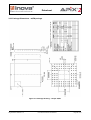
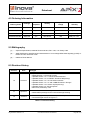
1
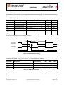
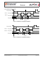
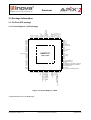
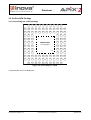
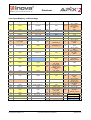
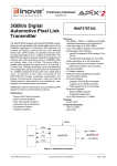
Datasheet
Revision 1.2
3GBit/s Digital
Automotive Pixel Link
Transmitter
The INAP375T together with an APIX2 receiver device
offers the next generation high speed digital serial link for
DISPLAY and CAMERA applications. It provides a
DC-balanced, AC coupled low latency, point-to-point link
over shielded twisted pair (STP) cables. Its scalable
physical layer provides bandwidth of up to 3 GBit/s at
lowest EMI. The INAP375T supports popular automotive
displays with video resolutions such as 1600x600 pixels
and refresh rates of up to 100Hz. The device offers a
flexible video interface, configurable to handle 1 or 2
independent video streams, with input interfaces such as
parallel RGB (1x24 Bit or 2x10 Bit) or openLDI (“LVDS”)
e.g. 2x (4 lanes + clock). Software adjustable driver
characteristics and configurable operating modes allow the
transmission of 3 GBit/s at distances of up to 12m over a
single pair of wires. In addition to the video transmission
the INAP375T provides completely independent Full
Duplex Communication channels. Using the internal
AShell protocol, data transfers are protected by error
detection and retransmission mechanisms. Offering a
Media Independent Interface (MII), the INAP375T can be
directly connected to an ethernet Media Access Controller,
offering full network capabilities through the APIX link.
Additionally, the link is optimized to carry low latency GPIO
signals for reset or synchronization purposes. The built-in
audio path allows synchronous transmission of up to
4 stereo audio channels, with highly precise clock regeneration at the receiver for high-end rear-seat entertainment
applications.
INAP375T
INAP375TAQ
Features:
• Backwards compatibility with APIX1
• 500 MBit/s, 1 GBit/s and 3 GBit/s sustained
downstream link bandwidth for video data
rates up to 2591 MBit/s
• up to 187.5 MBit/s upstream link bandwidth
• Supports 2 independent video streams
• Configurable video interface
– Parallel RGB (10,12,18 or 24 Bit)
– OpenLDI compliant LVDS interface[1] with
Single Pixel Format (18 or 24 Bit)
– Parallel Bulk Data Mode (10,12,18,24 Bit)
• Video resolutions up to HD resolutions
• Configurable full duplex communication
channel for up to 2 receivers (daisy chain)
• Media Independent Interface
• SPI data interfaces
• I²C Master interface
• GPIOs for direct signalling and camera
synchronization support
• Embedded AShell
• I²S Audio interface
– supports 16/24/32 Bit word length
– supports up to 192kHz sampling
– TDM support for up to 8 channels
• Diagnostic Features:
– Built-In PRBS Generator
– Embedded diagnostics
• Up to 12m distance at 3 GBit/s
Applications:
•
•
•
•
•
•
•
•
•
•
•
Central Information Displays
Round View Camera Systems
Head up Displays
Cluster Displays
Rear-Seat Entertainment Systems
Stereo Camera Systems
Rear View Camera Systems
Sensor Fusion Systems
Automotive Driver Assistance
Surveillance Systems
Inspection Systems
DS_INAP375T Revision 1.2
Packages:
• 100 pin LQFP
• 104 pin AQFN
Temperature/Quality:
• -40°C to +105°C
• AEC-Q100
Inova Semiconductors Confidential
Page 1 of 37
Datasheet
1.0 Characteristics
Mux
Video
Integrity support
2xLVDS
2x parallel
video
Audio
I2S
GPIO
GPIOs
I2C Dev.
EEPROM
I2C M
FIFO
FIFO
FIR
Framer
Serializer
Audio
APIX
Downstream
AShell
Mux
Ethernet
Data
I2C
EEPROM
Data
Configuration
MII /
Nibble
SPI M
Configuration,
Control, Status
Deserializer
Deframer
Reset
Osc.
Reset
10MHz
Phase
alignment
MCLK
CML
APIX
Upstream
VCO
SPI S
Figure 1-1: INAP375T Block Diagramm
1.1 Absolute Maximum Ratings
The absolute maximum ratings define values beyond which damage to the device may occur. Exposure to
absolute maximum rating conditions for extended periods may affect device reliability. The functional operation
of the device at these or any other conditions beyond the recommended operating ratings is not guaranteed.
Parameter
Symbol
Min.
Max.
Units
DC Supply Voltage
VDVDD,
VDVDD_XTAL,
VAVDD_LD
-0.5
5.0
V
Input Voltage
VVDD, VAVDD,
VAVDD_LVDS,
VVDD_XTAL
-0.5
3.0
V
ID
-20
+20
mA
Tstg
-55
+150
°C
260
°C
I/O Current (DC or transient any pin)
Storage Temperature
Max Soldering Temperature
TSLD / TSLD
Note
40 seconds maximum
Table 1-1: Absolute maximum ratings
DS_INAP375T Revision 1.2
Inova Semiconductors Confidential
Page 2 of 37
Datasheet
Parameter
Symbol
Min.
Max.
Units
Note
ESD Protection HBM
JEDEC JESD22/A114
-3
+3
kV
RD=1.5kΩ, CS=100pF
ESD Protection CDM
EIA/JEDEC JESD22/C101
-1
+1
kV
ESD Protection MM
EIA/JEDEC JESD22-A115A
-200
+200
V
Table 1-1: Absolute maximum ratings
1.2 Recommended Operating Conditions
Parameter
VVDD, VVDD_XTAL
VDVDD,
VDVDD_XTAL
VAVDD, VAVDD_VCO
VAVDD_LD
VAVDD_LVDS_PLL,
VAVDD_LVDS
VSUPPLY_NOISE
Ta
Description
Min.
Typ.
Max.
Units
Digital Core supply, Oscillator supply
1.71
1.8
1.89
V
Digital IO Supply,
Digital Oscillator supply
3.0
3.3
3.6
V
CML PHY supply voltage, VCO supply
1.71
1.8
1.89
V
CML IO supply
3.0
3.3
3.6
V
LVDS PLL & Core supply
1.71
1.8
1.89
V
50
mV
+105
°C
Analog and Digital Supply Noise
Ambient Temperature
-40
-
Note
Table 1-2: Recommended operating conditions
1.3 Electrical Characteristics
1.3.1 Serial Interface
The INAP375T downstream serial interface offers a flexible serial interface, with configurable pre-emphasis
and digital filter structure. Data dependent deterministic jitter components, mainly introduced by ISI due to cable attenuation, can be compensated by pre-emphasis and equalization. Therefore only periodic and random
jitter components are considered.
DS_INAP375T Revision 1.2
Inova Semiconductors Confidential
Page 3 of 37
Datasheet
Parameter
Effective serial bit rise and fall
time
CML Drive current
Symbol
Min.
Typ.
Max.
Units
trf_ser_effective
75
140
-
ps
Iout_dwn
15
-
-
mA
Note
Periodic Jitter
JPδ-δ
-
5.9
-
mUI
using PRBS12 signal; parameter
depends on application board, measured
on characterization
test board
Random Jitter
JRrms
-
1.6
-
ps
using PRBS12 signal
Table 1-3: Downstream interface characteristics (SD_DWN_OUT_P, SD_DWN_OUT_N)
Parameter
Differential input voltage range
Serial input common mode
range
Symbol
Min.
Max.
Units
Vdiff_in
± 50
± 500
mV
Vcmm_SDIN
GND +0.7V +
(Vdiff_in/2)
VAVDD +0.5V (Vdiff_in/2)
Note
V
Table 1-4: Upstream interface characteristics (SD_UP_IN_P,SD_UP_IN_N)
1.3.2 Supply Current
Parameter
Digital Core & Oscillator Supply current
Digital IO & Oscillator Supply Current
LVDS Core & PLL Supply Current
CML PHY Supply Current
VCO Supply Current
CML IO Supply Current
Symbol
Typ.a
Max.
Unit
IVDD + IVDD_XTAL
51
120
mA
IDVDD + IDVDD_XTAL
3
50
mA
IAVDD_LVDS +
IAVDD_LVDS_PLL
-
30
mA
IAVDD
111
190
mA
IAVDD_VCO
5
15
mA
IAVDD_LD
26
95
mA
Comment
see Figure 1-15
see Figure 1-15
Table 1-5: Supply current
a. 24bit RGB with 95MHz pixel clock and 5m cable setting
DS_INAP375T Revision 1.2
Inova Semiconductors Confidential
Page 4 of 37
Datasheet
1.3.3 Pixel Interface
The INAP375T‘s pixel interface can be configured to RGB or/and LVDS inputs. For further informations please
refer to the INAP375T user manual.
1.3.3.1 RGB Interface
Parameter
Description
Test Condition
Min.
Max.
Units
VIH
Input High Voltage
2.0
VDVDD
V
VIL
Input Low Voltage
0
0.8
V
IIH
Input High Current a
Vin = VDVDD
-10
10
μA
IIL
Input Low Current a
Vin = 0 V
-10
10
μA
VOH
Output High Voltage
IOH= -4mA
2.4
-
V
VOL
Output Low Voltage
IOL= 4mA
-
0.4
V
Table 1-6: RGB characteristics
a. input with Schmitt Trigger (current feedback of ~100μA)
Figure 1-2: RGB Interface Timing
The capturing edge of pixel clock can be set to rising or falling. For further information please refer to the
INAP375T user manual. fPIXEL_CLOCK = 1/tPERIOD . All values specified for TA=25°C.
Parameter
Description
Test Condition
fPIXEL_CLOCK
Pixel Clock Input Frequency
tSETUP
Setup Time Pixel Data To Pixel Clock
tHOLD
Hold Time Pixel Data to Pixel Clock
Min.
Max.
Units
5
120
MHz
slew rate 2V/ns
2
-
ns
slew rate 2V/ns
1
-
ns
Table 1-7: RGB Interface timing
DS_INAP375T Revision 1.2
Inova Semiconductors Confidential
Page 5 of 37
Datasheet
1.3.3.2 LVDS Interface[1]
OpenLDI interface with inputs according to LVDS specification[2]. Exceptions are listed at table 1-8.
Parameter
VOD
Description
Differential Output Voltage
Min.
Max.
Units
247
454
mV
1.125
1.375
V
VOS
Offset Voltage
VOD
|Change to VOD|
-
50
mV
VOS
|Change to VOs|
-
50
mV
ISA
Short Circuit Current
-
24
mA
IIN
Input Current
-
20
μA
VTH
Receiver Threshold Voltage
-
+100
mV
VIN
Input Voltage Range
0
1.8
V
fLVDS_CLK
LVDS Clock Frequency
5
80
MHz
Table 1-8: LVDS interface exceptions to TIA/EIA644 specification
DS_INAP375T Revision 1.2
Inova Semiconductors Confidential
Page 6 of 37
Datasheet
1.3.4 Data Interface
1.3.4.1 General Characteristics
The following characteristics are valid for SPI, SBDOWN, SBUP, GPIO, I²S, MII / Nibble data and I²C functionality. The pins I2C_SCL/INBOUND_TS and I2C_SD/OUTBOUND_TS are open drain outputs and require
external pull up circuitry. All values specified for TA=25°C.
Parameter
Symbol
Test Condition
Min.
Max.
Units
Input High Voltage
VIH
2.0
VDVDD
V
Input Low Voltage
VIL
0
0.8
V
Pull Down Current a
IIH_PD
Vin = VDVDD
30
120
μA
Input High Current
IIH
Vin = VDVDD
-10
10
μA
Input Low Current
IIL
Vin = 0 V
-10
10
μA
Output High Voltage b
VOH
IOH= -4mA, Figure 1-16
2.4
-
V
Output Low Voltage
VOL
IOL= 4mA, Figure 1-16
-
0.4
V
Output Rise Time b
tRO
CL=5pF
-
2.6
ns
Output Fall Time b
tFO
CL=5pF
-
2.1
ns
Table 1-9: General IO Characteristics
a. pins with internal pull down to GND
b. not relevant for open drain outputs
DS_INAP375T Revision 1.2
Inova Semiconductors Confidential
Page 7 of 37
Datasheet
1.3.4.2 SPI Slave Interface timing
Figure 1-3: SPI Slave Timing Diagram (CPHA=0)
Figure 1-4: SPI Slave Timing Diagram (CPHA=1)
The SPI Slave interface can be flexible configured with the parameters cfg_spi_s_cpol, cfg_spi_s_cpha. For
further informations please refer to the INAP375T user manual.
DS_INAP375T Revision 1.2
Inova Semiconductors Confidential
Page 8 of 37
Datasheet
Core clock frequency for APIX1 Mode = 125MHz and for APIX2 Mode = 187.5MHz. All values specified for
TA=25°C. tSCK = 1/fSCK.
APIX1 Mode
Parameter
Description
fSCK
SCK Clock Frequency
tSCKH
APIX2 Mode
Min.
Max.
Min
Max
Units
-
11
-
15
MHz
SCK High Time
45
-
33
-
ns
tSCKL
SCK Low Time
45
-
33
-
ns
tCSH
CS# High Time
20
-
15
-
ns
tCSS
CS# Setup Time
1/2 tSCK
-
1/2 tSCK
-
ns
tCSHO
CS# Hold Time
50
-
34
-
ns
tDISU
Data In Setup Time
16
-
12
-
ns
tDIHO
Data in Hold Time
16
-
12
-
ns
tDOV
Data Output Valid
-
40
-
29
ns
tDOHO
Data Output Hold Time
8
-
5
-
ns
tDODIS
Data Output Disable Time
-
50
-
45
ns
tA
Data Access Time
20
-
15
-
ns
Table 1-10: SPI Slave Interface characteristics (Read Access)
APIX1 Mode
Parameter
Description
fSCK
SCK Clock Frequency
tSCKH
APIX2 Mode
Min.
Max.
Min
Max
Units
-
31
-
41
MHz
SCK High Time
1/2 tSCK
-
1/2 tSCK
-
ns
tSCKL
SCK Low Time
1/2 tSCK
-
1/2 tSCK
-
ns
tCSH
CS# High Time
20
-
15
-
ns
tCSS
CS# Setup Time
1/2 tSCK
-
1/2 tSCK
-
ns
tCSHO
CS# Hold Time
50
-
34
-
ns
tDISU
Data In Setup Time
16
-
12
-
ns
tDIHO
Data In Hold Time
16
-
12
-
ns
Table 1-11: SPI Slave Interface characteristics (Write Only Access)
DS_INAP375T Revision 1.2
Inova Semiconductors Confidential
Page 9 of 37
Datasheet
1.3.4.3 SPI Master Interface timing
Figure 1-5: SPI Master Timing Diagram (CPHA=0)
Figure 1-6: SPI Master Timing Diagram (CPHA=1)
DS_INAP375T Revision 1.2
Inova Semiconductors Confidential
Page 10 of 37
Datasheet
The SPI Master interface can be flexible configured with the parameters cfg_spi_m_cpol, cfg_spi_m_cpha,
cfg_spi_m_clock_div, cfg_spi_m_cs_delay and cfg_byte_cnt. For further informations please refer to the
INAP375T user manual.
Core clock frequency for APIX1 Mode = 125MHz and for APIX2 Mode = 187.5MHz. All values specified for
TA=25°C.
APIX1 mode
APIX2 mode
Parameter
Description
Min.
Max.
Min.
Max.
Units
fSCKa
SCK Clock Frequency
0.007
15.63
0.011
23.44
MHz
tSCKH
SCK High Time
18
-
12
-
ns
tSCKL
SCK Low Time
22
-
16
-
ns
tCSH
CS# High Time
8
-
6
-
ns
tCSSb
CS# Setup Time (configurable)
125
-
85
-
ns
tCSHO
CS# Hold Time
40
-
30
-
ns
tDOV
Data Output Valid Time
-
8
-
10
ns
tDOHO
Data Output Hold Time
-10
-
-5
-
ns
tCSDOV
CS To Data Valid Time
-
140
-
100
ns
Table 1-12: SPI Master Interface characteristics
a. can be configured from core clock/16384 to core clock/8 by cfg_spi_m_clock_div
b. can be configured from 16 to 48 core clock cycles by cfg_spi_m_cs_delay and depends on CPOL, CPHA
DS_INAP375T Revision 1.2
Inova Semiconductors Confidential
Page 11 of 37
Datasheet
1.3.4.4 SPI EEPROM Master Interface timing
SPI_M_CS2#
tCSHO
tCSS
SPI_M_SCK
tSCKL
tSCKH
tDOV
SPI_M_SDO
SPI_M_SDI
tDIDIS
tDIHO
Figure 1-7: SPI EEPROM Master Timing Diagram
The SPI Master timings depend on the accuracy of the external 10MHz reference clock and are therefore listed
as typical values. For the EEPROM Master Timing the internal parameters are used: CPOL=0, CPHA=0,
tCSS delay = 48 wait core cycles and divider = core clock/128. Core clock frequency for APIX1 Mode =125MHz
and for APIX2 Mode =187.5MHz. All values specified for TA=25°C.
APIX1 mode
Parameter
Description
fSCK
APIX2 mode
Min.
Max.
Min
Max.
Units
SCK Clock Frequency
-
0.98
-
1.46
MHz
tSCKH
SCK High Time
-
512
-
341
ns
tSCKL
SCK Low Time
-
512
-
341
ns
tCSS
CS# Setup Time
896
-
597
-
ns
tCSHO
CS# Hold Time
30
-
30
-
ns
tDISU
Data In Setup Time
30
-
30
-
ns
tDIHO
Data In Hold Time
30
-
30
-
ns
tDOV
Data Output Valid Time
-5
5
-5
5
ns
Table 1-13: SPI Master EEPROM Interface characteristics
DS_INAP375T Revision 1.2
Inova Semiconductors Confidential
Page 12 of 37
Datasheet
1.3.4.5 I²C Interface timing
Figure 1-8: I2C Timing Diagram
The I2C timings depend on the accuracy of the external 10MHz reference clock and are therefore listed as typical values. All values specified for TA=25°C
Parameter
Description
Min.
Typ.
Max.
Units
fSCL
SCL Clock Frequency
Standard Mode
Fast Mode
-
-
100
400
kHz
tHIGH
SCL High Time
Standard Mode
Fast Mode
-
4.03
1.08
-
μs
tLOW
SCL Low Time
Standard Mode
Fast Mode
-
6.0
1.5
-
μs
tHDSTA
Hold Time (repeated) START conditon
Standard Mode
Fast Mode
-
4.0
1.0
-
μs
tHDDATa
Data Hold Time
Standard Mode
Fast Mode
-
4.0
1.0
-
μs
tSUDAT
Data Setup Time
Standard Mode
Fast Mode
-
2.0
0.5
-
μs
tSUSTA
Setup Time for repeated START conditon
Standard Mode
Fast Mode
-
6.03
1.58
-
μs
tSUSTO
Setup Time for STOP conditon
Standard Mode
Fast Mode
-
4.03
1.08
-
μs
Table 1-14: I2C Interface characteristics
DS_INAP375T Revision 1.2
Inova Semiconductors Confidential
Page 13 of 37
Datasheet
Parameter
Description
Min.
Typ.
Max.
Units
tBUF
Bus Free Time
Standard Mode
Fast Mode
-
10.0
2.5
-
μs
tf
fall time of SDA and SCL
Standard Mode
Fast Modeb
-
-
300
300
ns
tSP
pulse width of spike supression
Standard Mode
Fast Modec
-
-
50
ns
Table 1-14: I2C Interface characteristics
a. max. valid time (tVD) non-applicable, since device stretches the LOW period (tLOW) of the SCL signal
b. output buffers without slope control for falling edges, use series resistors to slow down falling egdes if needed
c. valid for SCL signal, no spike supression on SDA signal
1.3.4.6 RESET and Boot Strap timing
The INAP375T offers several boot strap pins to define, how the device will come up and check for a configuration
after boot up or hardware reset. The correct boot strap selection is necessary for proper operation of the INAP375T
device. For more information please refer to the INAP375T user manual.
Figure 1-9: Reset and Boot Strap Timing Diagram
For a valid Reset Low Time (tRESLOW) all supply voltages needs to be stable in the operating condition. At reset
release (rising edge of RESET#) a stable reference clock is required. All values specified for TA=25°C.
Parameter
Description
Min.
Typ.
Max.
Units
tRESLOW
Reset Low Time
1
-
-
ms
tBSU
Boot Strap In Setup Time
0
-
-
ns
tBHO
Boot Strap in Hold Time
500
-
-
ns
Table 1-15: Boot Strap Reset Timing
DS_INAP375T Revision 1.2
Inova Semiconductors Confidential
Page 14 of 37
Datasheet
1.3.4.7 GPIO Interface
1.3.4.7.1 GPIO Interface Downstream
The GPIO interface is only available in APIX2 mode. At transmitter side GPIO data input ports are sampled
asynchronously and transmitted to configurable GPIO output ports at receiver side. Sampling frequency can
be flexible configured using parameters GPIO Bandwidth (gpio_bw_dwn) and GPIO halved (gpio_bw_div). For
further information please refer to the INAP375T user manual. All values specified for TA=25°C.
Downstream
Bandwidth
GPIO
ports
GPIO
Bandwidth
GPIO
halved
Sampling Frequency.
Unit
3 GBit/s
1
high
off
26.768
MHz
3 GBit/s
1
low
off
6.696
MHz
3 GBit/s
1
high
on
13.393
MHz
3 GBit/s
1
low
on
3.348
MHz
3 GBit/s
2
high
off
13.393
MHz
3 GBit/s
2
low
off
3.348
MHz
3 GBit/s
2
high
on
6.696
MHz
3 GBit/s
2
low
on
unsupported
MHz
1 GBit/s
1
high
off
17.857
MHz
1 GBit/s
1
low
off
4.468
MHz
1 GBit/s
1
high
on
8.929
MHz
1 GBit/s
1
low
on
2.232
MHz
1 GBit/s
2
high
off
8.929
MHz
1 GBit/s
2
low
off
2.232
MHz
1 GBit/s
2
high
on
4.464
MHz
1 GBit/s
2
low
on
1.116
MHz
500 MBit/s
1
high
off
17.857
MHz
500 MBit/s
1
low
off
4.468
MHz
500 MBit/s
1
high
on
8.929
MHz
500 MBit/s
1
low
on
2.232
MHz
500 MBit/s
2
high
off
8.929
MHz
500 MBit/s
2
low
off
2.232
MHz
500 MBit/s
2
high
on
4.464
MHz
500 MBit/s
2
low
on
1.116
MHz
Table 1-16: GPIO Interface Downstream
DS_INAP375T Revision 1.2
Inova Semiconductors Confidential
Page 15 of 37
Datasheet
1.3.4.7.2 GPIO interface upstream
Transmitter GPIO upstream interface outputs GPIO data coming from either one or two APIX2 receiver devices. Output frequency can be configured using parameter GPIO Bandwidth (gpio_bw_up). For further informations please refer to the INAP375T user manual. All values specified for TA=25°C.
Number of
Rx
Upstream
Bandwidth
GPIO ports
GPIO
Bandwidth
Maximum Output frequency
Unit
1
187.5 MBit/s
1
high
13.39
MHz
1
187.5 MBit/s
1
low
3.35
MHz
1
187.5 MBit/s
2
high
13.39
MHz
1
187.5 MBit/s
2
low
3.35
MHz
1
62.5 MBit/s
1
high
4.46
MHz
1
62.5 MBit/s
1
low
1.12
MHz
1
62.5 MBit/s
2
high
4.46
MHz
1
62.5 MBit/s
2
low
1.12
MHz
2
187.5 MBit/s
1
high
6.69
MHz
2
187.5 MBit/s
1
low
3.35
MHz
2
187.5 MBit/s
2
high
6.96
MHz
2
187.5 MBit/s
2
low
3.35
MHz
2
62.5 MBit/s
1
high
2.23
MHz
2
62.5 MBit/s
1
low
1.12
MHz
2
62.5 MBit/s
2
high
2.23
MHz
2
62.5 MBit/s
2
low
1.12
MHz
Table 1-17: GPIO Interface Upstream
DS_INAP375T Revision 1.2
Inova Semiconductors Confidential
Page 16 of 37
Datasheet
1.3.4.8 Sideband Interface
1.3.4.8.1 Sideband Interface Downstream
The Sideband interface is only available in APIX1 mode. At transmitter side sideband data input ports are sampled asynchronously and transmitted to the corresponding output ports at receiver side. All values specified for
TA=25°C.
Downstream Bandwidth
Sampling frequency
Units
1 GBit / s
13.89
MHz
500 MBit / s
6.94
MHz
Table 1-18: Sideband Interface Downstream
1.3.4.8.2 Sideband Interface Upstream
Transmitter Sideband interface outputs sideband data coming from receiver side. All values specified for
TA=25°C.
Upstream Bandwidth
Maximum output frequency
Units
62.5 MBit / s
10.41
MHz
31.25 MBit / s
5.21
MHz
Table 1-19: Sideband Interface Upstream
1.3.4.9 MCLK clock output
The granularity of the frequency output of MCLK is definded by pulse width. For further informations please
refer to the INAP375T user manual. All values specified for TA=25°C.
Parameter
fMCLK_OUT
Description
Min
Max
Units
MCLK output frequency
2.953
187.5
MHz
Table 1-20: MCLK output frequency range
DS_INAP375T Revision 1.2
Inova Semiconductors Confidential
Page 17 of 37
Datasheet
1.3.4.10 I2S Audio Interface
fBCK = 1 / tPERIOD. All values specified for TA=25°C.
Figure 1-10: I2S Audio Interface Timing Diagram
Parameter
Description
Min
Max
Units
fBCK
I2S_BCK frequency
0.75
26.78
MHz
tHIGH
I2S_BCK high time
7
-
ns
tLOW
I2S_BCK low time
7
-
ns
tSETUP
Setup time
2
-
ns
tHOLD
Hold time
7
-
ns
Table 1-21: I2S Audio Interface Timing
DS_INAP375T Revision 1.2
Inova Semiconductors Confidential
Page 18 of 37
Datasheet
1.3.4.11 MII / NIBBLE Interface Timings
fMII_CLK = 1 / tPERIOD. All values specified for TA=25°C.
Figure 1-11: MII / NIBBLE Interface Timing Diagram Transmit
Figure 1-12: MII / NIBBLE Interface Timing Diagram Receive
Parameter
Description
Min
Typ
Max
Units
fMII_CLK
Clock Frequency
3.125
-
62.5
MHz
fMII_CLK
Clock Frequency
(100BASE-T)
-
25
-
MHz
tSETUP
Setup Time
9
-
-
ns
tHOLD
Hold Time
0
-
-
ns
tOUTV
Output Valid
1
-
7
ns
Table 1-22: MII / NIBBLE Interface Timings
DS_INAP375T Revision 1.2
Inova Semiconductors Confidential
Page 19 of 37
Datasheet
1.3.5 Reference Clock
The INAP375T requires an external clock source like a crystal or oscillator, acting as reference for the internal
PLL.
Parameter
fref_osc
Description
Min.
Typ.
Max.
Unit
Nominal Reference Frequency
-
10
-
MHz
Frequency Tolerance
-100
-
+100
ppm
Equivalent Series Resistance
-
-
80
Ohm
FTOL
ESRXTAL
Drive Level
see Table 1-24
Table 1-23: Reference clock requirements
The INAP375T core clock frequency is generated by an internal PLL controlled by an external 10 MHz crystal.
Alternatively a stable 10 MHz clock signal (3.3V CMOS TTL) can be directly connected to XTAL_IN with
XTAL_OUT left open. Figure 1-13 shows a typical crystal design required for the oscillator circuit. The values
for C1, C2 and R1 need to be selected to match the oscillation requirements of the crystal Q1.
Figure 1-13: Crystal clock schematic example
For resonance at the correct frequency, the crystal needs to be loaded with its specified load capacitance CL,
which is the value of capacitance used in conjunction with the oscillation unit. The INAP375T oscillator provides
some of the load with internal capacitance which is specified within the range of 10pF to 12.5pF. The remainder
is generated by the external capacitors and tuning capacitors labeled C1 and C2.
The load capacitance CL can be calculated from CL = Cint + C1//C2. E.g. selecting C1 and C2 with 15pF, CL
can be calculated to CL = 12.5pF + 7.5pF = 20pF.
DS_INAP375T Revision 1.2
Inova Semiconductors Confidential
Page 20 of 37
Datasheet
The crystal needs to be able to withstand the power dissipation, produced by the INAP375T. The power dissipation depends on the ESR of the crystal and is reflected by the maximum drive level of the crystal. Table 1-24
illustrates the power dissipation of the INAP375T and therefore the minimum drive level capabilities of the crystal at different crystal ESR levels.
Crystal ESR
INAP375T Power dissipation /
Minimum crystal drive level
Unit
30
77
μW
50
121
μW
80
179
μW
Table 1-24: Minimum Drive level
1.3.6 Power Up Sequencing
To avoid high IO currents, 1.8V supply voltages have to ramp before 3.3V supply on power-up. On power-down, 3.3V supply have to be powered down before 1.8V. On power-up all supply voltages have to rise
steadily from GND level up to the VCCMIN level without turn to negative direction. The ramping times must be
within the limits as specified in Figure 1-25. All 1.8V supplies have to be ramped up simultaneously starting
from GND according Figure 1-14. Reset has to be held low until all supplies reached recommended operating
conditions.
Figure 1-14: Steady voltage ramp-up
Parameter
tRAMP
Description
Min.
Typ.
Max.
Unit
Supply Ramp Up Time for all supplies GND to VCCmin
0.05
1
10
ms
Table 1-25: Power supply ramp-up time
DS_INAP375T Revision 1.2
Inova Semiconductors Confidential
Page 21 of 37
Datasheet
1.4 Typical Operating Characteristics
34
70
60
50
40
30
0
34
(IVDD+IVDD_XTAL)
supply current in mA
/(*$(&&)
+0
/(* $(&&)
+ 0
20
40
60
80
100
RGB pixel clock frequency in MHz
1
120
&)/0//"))5
6+0
!"$%!&'()$*+,-.
Figure 1-15: Typical supply current characteristics
Figure 1-16: Typical device I-V curve for 3.3V data interface IO under nominal conditions
DS_INAP375T Revision 1.2
Inova Semiconductors Confidential
Page 22 of 37
Datasheet
1.5 External Circuits
1.5.1 External Termination Resistors
There are no external termination resistors required. For both Upstream and Downstream the dedicated
50 Ohm termination resistors are integrated in the circuit.
1.5.2 External Coupling Capacitors
1.5.2.1 Downstream Coupling Capacitors
The serial data path in downstream direction requires coupling capacitors according Figure 1-17. Recommended value for all capacitors is 100nF (X7R) for all operation modi.
Figure 1-17: Downstream Coupling Capacitors
1.5.2.2 Upstream Coupling Capacitors
The serial data path in upstream direction requires coupling capacitors according Figure 1-18. Recommended
value for all capacitors is 100nF (X7R). Values depend on cable length and serial upstream data rate in combination with the selected APIX operation mode.
Figure 1-18: Upstream Coupling Capacitors
DS_INAP375T Revision 1.2
Inova Semiconductors Confidential
Page 23 of 37
Datasheet
2.0 Pin Description
Signal Name
PX[30:1]
Type
Ie
Description
Video Interface pin
SPI_M_SDO/
MII_CLK/
BST5
I/O f
SPI_M_SDO: SPI Master Data Output
MII_CLK: MII Interface Clock Output
BST5: Boot strap option 5 input
SPI_M_SDI/
MII_TX_EN
I
SPI_M_SDI: SPI Master Data Input
MII_TX_EN: MII Transmit Enable Input
SPI_M_SCK/
MII_RXD1/
BST2
I/O f
SPI_M_CS0#/
MII_RXD0
O
SPI_M_CS0#: SPI Master Chip-select 0 Output (Data Channel
0)
MII_RXD0: MII Receive Data Output 0
SPI_M_CS1#/
MII_RXD3/
O
SPI_M_CS1#: SPI Master Chip-select 1 Output (Data Channel
1)
MII_RXD3: MII Receive Data Output 3
SPI_M_CS2#
O
SPI_M_CS2#: SPI Master Chip-select 2 Output (Configuration)
SPI_S_SDO/
BST3
I/O f
SPI_M_SCK: SPI Master Serial Clock Output
MII_RXD1: MII Receive Data Output 1
BST2: Boot strap option 2 input
SPI_S_SDO: SPI Slave Data Output
BST3: Boot strap option 3 input
SPI_S_SDI
Ia
SPI Slave Data Input
SPI_S_SCK
Ia
SPI Slave Serial Clock Input
SPI_S_STALL/ MII_STALL
MII_COL/
BST4
I/O f
SPI_S_STALL:
High: SPI Slave not ready or buffer full
Low: SPI Slave ready to receive data
MII_STALL:
High: Nibble IF not ready or buffer full
Low: Nibble IF ready to receive data
MII_COL: MII Collision Detect output
BST4: Boot strap option 4 input
SPI_S_CS0#/
MII_TXD0/
SBDWN_DATA0
Ia
SPI_S_CS0#: SPI Slave Chip-select 0 Input (Data channel 0)
MII_TXD0: MII Transmit Data Input 0
SBDWN_DATA0: APIX1 Downstream data input 0
SPI_S_CS1#/
MII_TXD1/
SBDWN_DATA1
Ia
SPI_S_CS0#: SPI Slave Chip-select 1 input (Data channel 1)
MII_TXD1: MII Transmit Data input 1
SBDWN_DATA1: APIX1 Downstream data input 1
SPI_S_CS2#
Ia
SPI Slave Chip-select 2 input (Configuration)
Table 2-1: Pin description
DS_INAP375T Revision 1.2
Inova Semiconductors Confidential
Page 24 of 37
Datasheet
Signal Name
SPI_S_RW/
MII_TXD2
SPI_S_MB0/
MII_RXD2/
SBUP_DATA0/
BST1
SPI_S_MB1/
MII_RX_DV/
SBUP_DATA1/
BST6
MII_TXD3
Type
Description
SPI_S_RW: SPI Slave Read/Write input, only used in single
SPI mode
MII_TXD2: MII Transmit Data Input 2
I
I/O f
SPI_S_MB0: SPI Slave mailbox 0 output
MII_RXD2: MII Receive Data Output 2
SBUP_DATA0: APIX1 Upstream data output 0
BST1: Boot strap option 1 input
I/O f
SPI_S_MB1: SPI slave mailbox 1 output
MII_RX_DV: MII Receive Data Valid output
SBUP_DATA1: APIX1 Upstream data output 1
BST6: Boot strap option 6 input
I
MII_TXD3: MII Transmit Data Input 3
I²C_SCL/
INBOUND_TS
I/O b
I²C_SCL: I²C Clock output
INBOUND_TS: Inbound Nibble Data Target select output
I²C_SD/
OUTBOUND_TS
I/O b
I²C_SD: I²C Data pin
OUTBOUND_TS: Outbound Nibble Data Target select input
SD_UP_IN_P
Ic
Serial Link, Upstream Serial Link Input from RX
SD_UP_IN_N
Ic
Serial Link, Upstream Serial Link Input from RX
SD_DWN_OUT_N
Oc
Serial Link, Downstream Serial Link output to RX
SD_DWN_OUT_P
Oc
Serial Link, Downstream Serial Link output to RX
XTAL_IN
I
10MHz Oscillator input
XTAL_OUT
O
10MHz Oscillator output
I2S_FRCK
Ia
I2S Interface, Frame clock input
I2S_BCK
Ia
I2S Interface, Bit clock input
I2S_SDATA
Ia
I2S Interface, Data input
I2S_MCLK
I/O
I2S Interface, Master Clock input/output
I/O
GPIO1: General purpose I/O
SBDWN_CLK: Sampling clock output for SBDWN_DATA[1:0]
(APIX1 Mode)
DEBUG Interface : Debug Output Pin1
GPIO0/SBUP_CLK
I/O
GPIO0: General purpose I/O
SBUP_CLK: Sampling clock output for SBUP_DATA[1:0]
(APIX1 Mode)
DEBUG Interface : Debug Output Pin0
STATUS
O
STATUS: Device status output
RESET#
Id
Reset
GPIO1/SBDWN_CLK
Table 2-1: Pin description
DS_INAP375T Revision 1.2
Inova Semiconductors Confidential
Page 25 of 37
Datasheet
Signal Name
PLL_VCO_TUNE
Type
Description
O
reserved, do not connect
DVDD
Power
Digital I/O power supply
AVDD_LVDS_PLL
Power
LVDS PLL power supply
VDD
Power
Core supply
AVDD_LVDS
Power
LVDS I/O power supply
AVDD_LD
Power
Serial Link I/O Power supply
AVDD
Power
Serial Link core power supply
AVDD_VCO
Power
Serial Link VCO Power supply
VDD_XTAL
Power
10MHz Oscillator core supply
DVDD_XTAL
Power
10MHz Oscillator digital supply
GND_XTAL
GND
10MHz Oscillator Ground
GND
GND
Ground
Exposed PAD (EP)
GND
must be connected to GND-plane
TEST
Ia
reserved, pull down external over 100kOhm to GND
Table 2-1: Pin description
a. with internal pull-down
b. n-channel open drain
c. CML interface
d. schmitt trigger input
e. external 100 Ohm termination is required in case of LDI input
f. BST pins require defined level during hardware reset (pull-up or pull-down)
DS_INAP375T Revision 1.2
Inova Semiconductors Confidential
Page 26 of 37
Datasheet
2.1 Reset
The pin RESET# triggers an asynchronous reset (active low) and can be activated any time. This reset erases
all configuration settings. Please see Table 2-2 for the status of all pins during reset.
Signal Name
Reset State
Functional State
PX[30:1]
Input
Input
SPI_M_SDO / MII_CLK / BST5
Input
Output
SPI_M_SDI / MII_TX_EN
Input
Input
SPI_M_SCK / MII_RXD1 / BST2
Input
Output
SPI_M_CS0# / MII_RXD0
Output
Output
SPI_M_CS1# / MII_RXD3/
Output
Output
SPI_M_CS2#
Output
Output
SPI_S_SDO / BST3
Input
Output
SPI_S_SDI
Input
Input
SPI_S_SCK
Input
Input
SPI_S_STALL / MII_COL / BST4
Input
Output
SPI_S_CS0# / MII_TXD0 / SBDWN_DATA0
Input
Input
SPI_S_CS1# / MII_TXD1 / SBDWN_DATA1
Input
Input
SPI_S_CS2#
Input
Input
SPI_S_RW / MII_TXD2
Input
Input
SPI_S_MB0 / MII_RXD2 / SBUP_DATA0 / BST1
Input
Output
SPI_S_MB1 / MII_RX_DV / SBUP_DATA1 / BST6
Input
Output
MII_TXD3
Input
Input
I²C_SCL / INBOUND_TS
Tri-State
Tri-State / Output
I²C_SD / OUTBOUND_TS
Tri-State
Tri-State / Input / Output
I2S_FRCK
Input
Input
I2S_BCK
Input
Input
I2S_SDATA
Input
Input
I2S_MCLK
Tri-State
Tri-State / Input / Output
GPIO1 / SBDWN_CLK
Input
Input / Output
GPIO0 / SBUP_CLK
Input
Input / Output
Output
Output
STATUS
Table 2-2: Reset States
DS_INAP375T Revision 1.2
Inova Semiconductors Confidential
Page 27 of 37
Datasheet
3.0 Package Information
3.1 100 Pin LQFP package
3.1.1 Pinout Diagram - LQFP package
$&
!
!
!
!
Figure 3-1: Pinout diagram - LQFP
* Exposed PAD connect to GND-plane
DS_INAP375T Revision 1.2
Inova Semiconductors Confidential
Page 28 of 37
Datasheet
3.1.2 Signal Mapping - LQFP package
Pin
Signal
Pin
Signal
LQFP
pin
Signal
LQFP
pin
Signal
1
PX15
27
SPI_S_CS2#
53
XTAL_OUT
79
PX27
28
SPI_S_RW /
MII_TXD2
54
VDD_XTAL
80
PX26
29
SPI_S_MB0 /
MII_RXD2 /
SBUP_DATA0 /
BST1
55
DVDD_XTAL
81
PX25
SPI_S_MB1 /
MII_RX_DV/
SBDWN_DATA1/
BST6
56
I2S_FRCK
82
PX30
2
3
PX4
PX5
4
PX6
30
5
PX3
31
MII_TXD3
57
I2S_BCK
83
PX29
58
I2S_SDATA
84
PX24
VDD
85
PX23
6
PX2
32
I2C_SCL /
INBOUND_TS
7
DVDD
33
I2C_SD /
OUTBOUND_TS
59
8
GND
34
GND
60
GND
86
PX20
9
AVDD_LVDS
35
VDD
61
I2S_MCLK
87
AVDD_LVDS_PLL
10
PX1
36
VDD
62
GPIO1
88
GND
11
SPI_M_SDO /
MII_CLK /
BST5
37
SD_UP_IN_P
63
GPIO0
89
VDD
12
SPI_M_SDI /
MII_TX_EN
38
SD_UP_IN_N
64
STATUS
90
GND
13
SPI_M_SCK /
MII_PXD1 /
BST2
39
GND
65
TEST
91
PX8
14
SPI_M_CS0# /
MII_RXD0
40
GND
66
RESET#
92
PX7
15
SPI_M_CS1# /
MII_RXD3
41
AVDD_VCO
67
AVDD_LVDS
93
PX14
16
GND
42
PLL_VCO_TUNE
68
GND
94
PX13
17
VDD
43
AVDD
69
DVDD
95
PX10
18
SPI_M_CS2#
44
GND
70
PX16
96
PX9
19
SPI_S_SDO /
BST3
71
PX17
97
PX12
45
SD_DWN_OUT_N
20
SPI_S_SDI
46
SD_DWN_OUT_P
72
PX21
98
PX11
21
SPI_S_SCK
47
AVDD_LD
73
PX22
99
DVDD
22
SPI_S_STALL /
MII_COL /
BST4
48
GND
74
PX18
100
GND
23
SPI_S_CS0# /
MIITXD0 /
SBDWN_DATA0
49
AVDD_LD
75
PX19
24
DVDD
50
AVDD
76
GND
25
GND
51
XTAL_GND
77
DVDD
26
SPI_S_CS1# /
MII_TXD1 /
SBDWN_DATA1
52
XTAL_IN
78
PX28
Video Interface
Data Interface
Serial Interface
Table 3-1: Signal Mapping List - LQFP
DS_INAP375T Revision 1.2
Inova Semiconductors Confidential
Page 29 of 37
Datasheet
Supply Name
Pins
Supply Name
Pins
GND
8, 16, 25, 34, 39, 40,
44, 48, 60, 68, 76, 88,
90, 100
43, 50
AVDD_VCO
41
AVDD_LD
47, 49
VDD_XTAL
54
AVDD_LVDS
9, 67
DVDD_XTAL
55
AVDD_LVDS_PLL
87
XTAL_GND
51
VDD
17, 35, 36, 59, 89
DVDD
7, 24, 69, 77, 99
AVDD
Table 3-2: Supply Pins - LQFP
DS_INAP375T Revision 1.2
Inova Semiconductors Confidential
Page 30 of 37
Datasheet
3.1.3 Package Dimensions - LQFP package
Figure 3-2: Package Drawing - 100 pin LQFP
DS_INAP375T Revision 1.2
Inova Semiconductors Confidential
Page 31 of 37
Datasheet
3.2 104 Pin aQFN Package
3.2.1 Pinout Diagram - aQFN package
A2
A3
A4
A5
A6
A7
A8
A9
A10
A11
B1
B2
B3
B4
B5
B6
B7
B8
B9
B10
B11
B12
C1
C2
C3
C4
C5
C6
C7
C8
C9
C10
C11
C12
D1
D2
D3
D10
D11
D12
E1
E2
E3
E10
E11
E12
F1
F2
F3
F10
F11
F12
G1
G2
G3
G10
G11
G12
H1
H2
H3
H10
H11
H12
J1
J2
J3
J10
J11
J12
K1
K2
K3
K4
K5
K6
K7
K8
K9
K10
K11
K12
L1
L2
L3
L4
L5
L6
L7
L8
L9
L10
L11
L12
M2
M3
M4
M5
M6
M7
M8
M9
M10
M11
INAP375TAQ
104 pad aQFN
EP*
Figure 3-3: Pinout diagram - aQFN
* Exposed PAD connect to GND-plane
DS_INAP375T Revision 1.2
Inova Semiconductors Confidential
Page 32 of 37
Datasheet
3.2.2 Signal Mapping - aQFN package
Pin
Signal
Pin
Signal
Pin
Signal
Pin
Signal
A2
PX19
C6
RESET#
G3
VDD
K12
SPI_S_MB0 /
MII_RXD2 /
SBUP_DATA0 /
BST1
A3
PX21
C7
I2S_MCLK
G10
VDD
L1
PX12
A4
PX16
C8
I2S_BCK
G11
NC
L2
PX11
A5
AVDD_LVDS
C9
VDD_XTAL
G12
SD_UP_IN_P
L3
PX15
A6
STATUS
C10
XTAL_GND
H1
GND
L4
PX6
A7
GPIO0
C11
GND
H2
GND
L5
DVDD
A8
GND
C12
SD_DWN_OUT_P
H3
PX7
L6
PX1
A9
I2S_SDATA
D1
NC
H10
I2C_SCL /
INBOUND_TS
L7
SPI_M_SCK /
MII_PXD1 /
BST2
A10
DVDD_XTAL
D2
PX30
H11
I2C_SD /
OUTBOUND_TS
L8
GND
A11
XTAL_IN
D3
PX26
H12
GND
L9
SPI_S_SDO /
BST3
B1
PX28
D10
AVDD_LD
J1
PX8
L10
SPI_S_STALL /
MII_COL /
BST4
B2
DVDD
D11
NC
J2
PX14
L11
DVDD
B3
PX18
D12
B4
PX17
E1
B5
GND
SD_DWN_OUT_N
PX23
J3
PX10
L12
SPI_S_CS1# /
MII_TXD1 /
SBDWN_DATA1
J10
SPI_S_RW /
MII_TXD2
M2
GND
M3
PX5
E2
PX24
J11
SPI_S_MB1 /
MII_RX_DV/
SBDWN_DATA1/
BST6
B6
TEST
E3
PX29
J12
MII_TXD3
M4
PX3
B7
GPIO1
E10
GND
K1
PX13
M5
GND
B8
VDD
E11
AVDD
K2
PX9
M6
SPI_M_SDO /
MII_CLK /
BST5
B9
I2S_FRCK
E12
AVDD_VCO
K3
DVDD
M7
SPI_M_SDI /
MII_TX_EN
B10
XTAL_OUT
F1
GND
K4
PX4
M8
SPI_M_CS1# /
MII_RXD3
B11
AVDD
F2
AVDD_LVDS_PLL
K5
PX2
M9
VDD
B12
AVDD_LD
F3
PX20
K6
AVDD_LVDS
M10
SPI_S_SDI
C1
PX25
F10
GND
K7
SPI_M_CS0# /
MII_RXD0
M11
SPI_S_CS0# /
MIITXD0 /
SBDWN_DATA0
C2
PX27
F11
GND
K8
SPI_M_CS2#
C3
GND
F12
SD_UP_IN_N
K9
SPI_S_SCK
C4
PX22
G1
GND
K10
GND
C5
DVDD
G2
VDD
K11
SPI_S_CS2#
Video Interface
Data Interface
Serial Interface
Table 3-3: Signal Mapping List - aQFN
DS_INAP375T Revision 1.2
Inova Semiconductors Confidential
Page 33 of 37
Datasheet
Supply Name
Pins
Supply Name
Pins
GND
A8, B5, C3, C11, E10,
F1, F10, F11, G1, H1,
H2, H12, K10, L8, M2,
M5
B11, E11
AVDD_VCO
E12
AVDD_LD
B12, D10
VDD_XTAL
C9
AVDD_LVDS
A5, K6
DVDD_XTAL
A10
AVDD_LVDS_PLL
F2
XTAL_GND
C10
VDD
B8, G2, G3, G10, M9
DVDD
B2, C5, K3, L5, L11
AVDD
Table 3-4: Supply Pins - aQFN
DS_INAP375T Revision 1.2
Inova Semiconductors Confidential
Page 34 of 37
Datasheet
3.2.3 Package Dimensions - aQFN package
Figure 3-4: Package Drawing - 104 pin aQFN
DS_INAP375T Revision 1.2
Inova Semiconductors Confidential
Page 35 of 37
Datasheet
4.0 Ordering Information
Device /
Ordering Code
Package
RoHS
compliant
Quality
Temperature
Range
Minimum Order
Quantity
INAP375T
LQFP100
yes
AEC-Q100
-40°C to +105°C
90 pcs / traý
INAP375T-R1
LQFP100
yes
AEC-Q100
-40°C to +105°C
1000 pcs / reel
INAP375TAQ
aQFN104
yes
AEC-Q100
tbd
260 pcs / traý
INAP375TAQ-R2
aQFN104
yes
AEC-Q100
tbd
2000 pcs / reel
Table 4-1: Ordering Information
5.0 Bibliography
[1] – OpenLDI Specification, National Semiconductors, Rev. 0.95, 13th of May 1999
[2] – ANSI/TIA/EIA-644-1995 Electrical Characteristics of Low Voltage Differential Signaling (LVDS) Interface Circuits, November 1995
[3] – INAP375T User Manual
6.0 Revision History
Revision
Date
Changes
1.0
Oct 2012
•
•
•
•
•
•
•
•
•
Updated Section 1.3.1 "Serial Interface"
Added Section 1.5 "External Circuits"
Updated Section 1.3.4.1 "General Characteristics"
Updated Section 1.3.4.6 "RESET and Boot Strap timing"
Updated Section 1.3.4.10 "I2S Audio Interface"
Updated Section 1.3.4.11 "MII / NIBBLE Interface Timings"
Updated Section 1.3.6 "Power Up Sequencing"
Updated Section 2.0 "Pin Description"
Removed „Preliminary“ note
1.1
Apr 2013
• Added Section 4.0 "Ordering Information"
• Added AQFN package Pinout List and Package Drawing
1.2
Jul 2013
• Removed support for openLDI dual pixel format (“Dual LVDS Mode”).
• Corrected Signal names in Figure 1-7
Table 6-1: Revision History
DS_INAP375T Revision 1.2
Inova Semiconductors Confidential
Page 36 of 37
Datasheet
Inova Semiconductors GmbH
Grafinger Str. 26
D-81671 Munich / Germany
Phone: +49 (0)89 / 45 74 75 - 60
Fax:
+49 (0)89 / 45 74 75 - 88
Email: [email protected]
URL:
http://www.inova-semiconductors.com
is a registered trademark of Inova Semiconductors GmbH
All other trademarks or registered trademarks are the property of their respective holders.
Inova Semiconductors GmbH does not assume any liability arising out of the applications or use of the product described herein; nor does
it convey any license under its patents, copyright rights or any rights of others.
Inova Semiconductors products are not designed, intended or authorized for use as components in systems to support or sustain life, or
for any other application in which the failure of the product could create a situation where personal injury or death may occur. The information contained in this document is believed to be current and accurate as of the publication date. Inova Semiconductors GmbH reserves
the right to make changes at any time in order to improve reliability, function or performance to supply the best product possible.
Inova Semiconductors GmbH assumes no obligation to correct any errors contained herein or to advise any user of this text of any correction if such be made.
© Inova Semiconductors 2013
DS_INAP375T Revision 1.2
Inova Semiconductors Confidential
Page 37 of 37