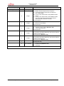
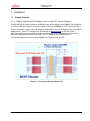
1
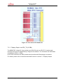
Fujitsu Semiconductor Europe User Manual FSEUGCC-UM_SK-88F335-01_Rev1.0 INDIGO2-S STARTERKIT SK-88F335-01 USER MANUAL Indigo2-S Starterkit SK-88F335-01 Revision History Date Issue 18.02.2013 Rev0.1 Herbert Hönig First draft 25.03.2103 Rev1.0 Herbert Hönig First Release This document contains 22 pages. FSEUGCC-UM_SK-88F335-01-Rev1.0 -2- © Fujitsu Semiconductor Europe GmbH Indigo2-S Starterkit SK-88F335-01 Trademarks APIX™ is a registered trademark of Inova Semiconductors GmbH, Grafinger Str. 26, 81671 Munich, Germany ARM™ is a registered trademark of ARM Limited in UK, USA and Taiwan. ARM™ is a trademark of ARM Limited in Japan and Korea. ARM Powered™ logo is a registered trademark of ARM Limited in Japan, UK, USA, Korea and Taiwan. PrimeCell® is owned by ARM Limited. CAN®, Controller Area Network® is registered trademarks of Bosch Corporation in the United States and other countries. I2C® is a registered trademark of Philips Semiconductor Corporation in the United States and other countries. SPI®, Serial Peripheral Interface, is a registered trademark of Motorola Corporation in the United States and other countries. RSDS® and PPDS® are registered trademarks of National Semiconductor. Truevision® is a registered trademark of Truevision, Inc. TGA® is a trademark of Truevision, Inc. Other system names or product names which may appear in this document are the trademarks of the respective company or organization. FSEUGCC-UM_SK-88F335-01-Rev1.0 -3- © Fujitsu Semiconductor Europe GmbH Indigo2-S Starterkit SK-88F335-01 Warranty and Disclaimer To the maximum extent permitted by applicable law, Fujitsu Semiconductor Europe GmbH restricts its warranties and its liability for all products delivered free of charge (eg. software include or header files, application examples, target boards, evaluation boards, engineering samples of IC’s etc.), its performance and any consequential damages, on the use of the Product in accordance with (i) the terms of the License Agreement and the Sale and Purchase Agreement under which agreements the Product has been delivered, (ii) the technical descriptions and (iii) all accompanying written materials. In addition, to the maximum extent permitted by applicable law, Fujitsu Semiconductor Europe GmbH disclaims all warranties and liabilities for the performance of the Product and any consequential damages in cases of unauthorised decompiling and/or reverse engineering and/or disassembling. Note, all these products are intended and must only be used in an evaluation laboratory environment. 1. Fujitsu Semiconductor Europe GmbH warrants that the Product will perform substantially in accordance with the accompanying written materials for a period of 90 days form the date of receipt by the customer. Concerning the hardware components of the Product, Fujitsu Semiconductor Europe GmbH warrants that the Product will be free from defects in material and workmanship under use and service as specified in the accompanying written materials for a duration of 1 year from the date of receipt by the customer. 2. Should a Product turn out to be defect, Fujitsu Semiconductor Europe GmbH´s entire liability and the customer´s exclusive remedy shall be, at Fujitsu Semiconductor Europe GmbH´s sole discretion, either return of the purchase price and the license fee, or replacement of the Product or parts thereof, if the Product is returned to Fujitsu Semiconductor Europe GmbH in original packing and without further defects resulting from the customer´s use or the transport. However, this warranty is excluded if the defect has resulted from an accident not attributable to Fujitsu Semiconductor Europe GmbH, or abuse or misapplication attributable to the customer or any other third party not relating to Fujitsu Semiconductor Europe GmbH. 3. To the maximum extent permitted by applicable law Fujitsu Semiconductor Europe GmbH disclaims all other warranties, whether expressed or implied, in particular, but not limited to, warranties of merchantability and fitness for a particular purpose for which the Product is not designated. 4. To the maximum extent permitted by applicable law, Fujitsu Semiconductor Europe GmbH´s and its suppliers´ liability is restricted to intention and gross negligence. NO LIABILITY FOR CONSEQUENTIAL DAMAGES To the maximum extent permitted by applicable law, in no event shall Fujitsu Semiconductor Europe GmbH and its suppliers be liable for any damages whatsoever (including but without limitation, consequential and/or indirect damages for personal injury, assets of substantial value, loss of profits, interruption of business operation, loss of information, or any other monetary or pecuniary loss) arising from the use of the Product. Should one of the above stipulations be or become invalid and/or unenforceable, the remaining stipulations shall stay in full effect FSEUGCC-UM_SK-88F335-01-Rev1.0 -4- © Fujitsu Semiconductor Europe GmbH Indigo2-S Starterkit SK-88F335-01 Table of Contents 1 Introduction ........................................................................................................ 6 1.1 System Features ................................................................................................... 6 1.2 Mechanical Dimensions ....................................................................................... 6 2 Information and Support on the Internet ......................................................... 7 3 System Overview ............................................................................................... 8 4 Quick Start ......................................................................................................... 9 5 Board Layout.................................................................................................... 11 6 Board/System Configuration DIP Switches ................................................... 12 6.1 DIP Switch SW7 (Bootstrap Modes) .................................................................. 12 6.2 DIP Switch SW6 (External Interfaces and Peripherals) .................................... 14 7 Interfaces .......................................................................................................... 15 7.1 Display Outputs .................................................................................................. 15 7.1.1 7.1.2 7.2 Display Outputs via Pin Headers (also for Glyn TFT Family Displays) ......................... 15 Display Output via APIX_TX (3 GBit) ............................................................................ 16 Mini-USB to RS232 / HOST SPI Interface........................................................... 17 7.2.1 7.2.2 HOST SPI Interface....................................................................................................... 17 RS232 (UART) Ports ..................................................................................................... 17 7.3 LIN Interface ........................................................................................................ 17 7.4 Sound .................................................................................................................. 18 7.5 Temperature Sensor (NTC) ................................................................................ 18 7.6 Light Sensor (Photo Cell) ................................................................................... 18 7.7 Extension Board Connectors ............................................................................. 18 7.7.1 7.7.2 7.7.3 TFT Board Connector X16 ............................................................................................ 18 Stepper Motor Board Connector X15 ............................................................................ 18 LED Board Connector X14 ............................................................................................ 18 8 Power Supply ................................................................................................... 19 9 Memory ............................................................................................................. 20 9.1 10 QUAD-SPI Flash (U3) .......................................................................................... 20 Appendix ....................................................................................................... 21 10.1 Literature and References Used ........................................................................ 21 10.2 Figures................................................................................................................. 22 FSEUGCC-UM_SK-88F335-01-Rev1.0 -5- © Fujitsu Semiconductor Europe GmbH Indigo2-S Starterkit SK-88F335-01 1 Introduction 1.1 System Features This section provides an overview of the features of the SK-88F335-01 (Indigo2-S Starterkit). 1x UART interface via FTDI USB serial converter (USB to RS232) HOST SPI interface via FTDI USB serial converter (USB to HOST SPI) LIN interface (pin header 2.54 mm) Quad-SPI Flash (10 MBit Spansion) on board 1x APIX-TX interface (3 Gbit) – Loopthrough mode 1x APIX-RX interface (3 Gbit) 1x FFC video output (RGB666) with touch controller (for the direct connection of Glyn EDT display family devices) 1x video output on pin header 1.27mm pitch (RGB888) 3x user buttons and 3x user LEDs (programmable via GPIOs) Sound amplifier output NTC Sensor and Photocell Sensor on GPIOs usable Connectors for LED Driver Boards, Stepper Motor Boards and Display Boards Most of the interfaces can be accessed separately via control switches on the board, making possible the use of all multiplex modes of the MB88F335 ‘Indigo2-S'. 1.2 Mechanical Dimensions - PCB (components not mounted): 150 x 150 mm - Dimensions with mounted connectors: 650 x 155 mm - Height (with spacing bolts): 40 mm FSEUGCC-UM_SK88F335-01-Rev1.0 -6- © Fujitsu Semiconductor Europe GmbH Indigo2-S Starterkit SK-88F335-01 2 Information and Support on the Internet The functional details of the MB88F335 'Indigo2-S' device can be found in the latest Hardware Manual. Please contact your local Fujitsu Sales Representative to obtain the last version. For support and downloads concerning the SK-88F335-01 board, please refer to the following locations: http://www.fujitsu.com/emea/services/microelectronics/gdc/gdcdevices/mb88f335-indigo2S.html (select the 'Development Tools' tab) FSEUGCC-UM_SK-88F335-01-Rev1.0 -7- © Fujitsu Semiconductor Europe GmbH Indigo2-S Starterkit SK-88F335-01 3 System Overview The Indigo2-S Starterkit itself is a complete evaluation system using a display, which is the best way to work with an APIX source like Emerald-P, Jade-D, or a MCU. The Fujitsu Developer Suite is a good choice for debugging and working with the Chip. It provides easy access to registers with many functionality and flashing options. Please find more information about the Fujitsu Developer Suite here: http://www.fujitsu.com/emea/services/microelectronics/gdc/swtools/fj-developer-suite.html Figure 3-1: System Overview FSEUGCC-UM_SK88F335-01-Rev1.0 -8- © Fujitsu Semiconductor Europe GmbH Indigo2-S Starterkit SK-88F335-01 4 Quick Start Before powering-up the board, please ensure to have: • A DC-power supply that can deliver a voltage in the range of 9...18V at max. 1.5A (12V is recommended). The internal pin has to be connected to positive (+), the outer ring has to be connected to ground (-). A suitable power supply can also be delivered by Fujitsu (please contact your Fujitsu Sales Representative, if required). • The correct switch settings on the board (e.g. pin multiplex settings, interfaces to be used) according to your application. The default settings of the switches are described in this document. In order to bring the system into operation, please execute the following steps: • Install the drivers for the FTDI components on your board. If necessary, obtain the latest version from the FTDI website* * http://www.ftdichip.com/Drivers/VCP.htm http://www.ftdichip.com/Support/Documents/InstallGuides.htm • Connect a mini USB cable to J3 and the other end to your PC. The SK-88F335-01 Indigo2-S Starterkit will be automatically recognized and four new COM ports will be installed as follows: o 'USB Serial Converter A': can be used as the HOST SPI interface o 'USB Serial Converter C': can be used as the UART0 interface Note: Windows may not use exactly these names. However, the third COM port installed is the one that is required for the next installation step. • A terminal program such as Tera Term (http://ttssh2.sourceforge.jp) can be used for serial communication, used with the following configuration: o Baud rate: 115.200 bps o Data: 8 bits o Stop bit: 1 bit o Parity: none o Flow Control: none • Connect the terminal program to port: 'USB Serial Converter C' • Connect a FFC cable to the Glyn TFT panel and to X1. A resolution of 800 x 480 pixels can be used with the standard TFT. • With TFT connected, proceed to connect the external DC-power supply to X11 (at 12V, a current supply of approx. 500 mA will be needed during power up mode) • Switch on your SK-88F335-01 Board using switch SW1 (large switch on the bottom lefthand corner of the PCB), and check that LEDs D11 and D12 light up. • After the board has powered up, a Splash screen will be shown. • When using APIX, additional settings are necessary as, depending of the mode used, a different configuration is needed. Therefore, no default setting will be provided here. FSEUGCC-UM_SK-88F335-01-Rev1.0 -9- © Fujitsu Semiconductor Europe GmbH Indigo2-S Starterkit SK-88F335-01 Figure 4-1: TFT Cable connected Figure 4-2: Splash screen FSEUGCC-UM_SK88F335-01-Rev1.0 - 10 - © Fujitsu Semiconductor Europe GmbH Indigo2-S Starterkit SK-88F335-01 5 Board Layout In the standard delivery form, the board layout is as shown in the diagram below: Display Extension Connector RGB 888 Pin Header DIP Switch SW7 Glyn TFT Connector DIP Switch SW6 Stepper Motor Connectors LED Extension Connector RESET Switch POWER Switch 3x Switch/LED via GPIO POWER Connector APIX In/Out Connectors USB Connector for HOST SPI and USART Figure 5-1: Standard Board Layout/Assembly FSEUGCC-UM_SK-88F335-01-Rev1.0 - 11 - © Fujitsu Semiconductor Europe GmbH Indigo2-S Starterkit SK-88F335-01 6 Board/System Configuration DIP Switches The Indigo2-S Starterkit is configured using a series of DIP-switches. The functionality of these groups of switches is described in the following sections. 6.1 DIP Switch SW7 (Bootstrap Modes) on Default Settings 7 8 TEST_ENABLE 6 unused 5 Config 5 4 Config 4 Config 1 3 Config 3 2 Config 2 1 Config 0 SW7 Figure 6-1: DIP Switch SW7 FSEUGCC-UM_SK88F335-01-Rev1.0 - 12 - © Fujitsu Semiconductor Europe GmbH Indigo2-S Starterkit SK-88F335-01 Part Number (Group) Switch Switch Name SW7 (System) * 1 Config 0 Command sequencer boot mode select: 2 Config 1 b00: Disable command sequencer boot sequence b01: Command sequencer starts with boot sequence from internal Flash b10: Power up with default APIX mode (500Mbit/s APIX2 mode) b11: Power up with default APIX mode (500Mbit/s APIX2 mode) and execute boot sequence from internal Flash afterwards. (DEFAULT ON/ON) Internal pull-down 3 Config 2 Set to 1 (DEFAULT ON) b1: HOST SPI in FTDI Mode Internal pull-down Config 3 APIX oscillator mode: b0: External crystal oscillator (DEFAULT OFF) b1: Clock input (via XI pin) Internal pull-down Config 4 Not used. Can be read by Command Sequencer and used for selection of different boot sequences Internal pull-down (DEFAULT OFF) 6 Config 5 Not used. Can be read by Command Sequencer and used for selection of different boot sequences Internal pull-down (DEFAULT OFF) 7 - 8 TEST ENABLE 4 5 Function Unused (leave OFF) Reserved – do not change! 0 = Normal Mode (DEFAULT OFF) 1 = Test Mode * SW7 can be found on page 2 of the schematic (Rev1.0). FSEUGCC-UM_SK-88F335-01-Rev1.0 - 13 - © Fujitsu Semiconductor Europe GmbH Indigo2-S Starterkit SK-88F335-01 6.2 DIP Switch SW6 (External Interfaces and Peripherals) on Default Settings 4 5 6 7 8 unused unused Use NTC Use Foto-Sensor Use LIN Interface 3 Use HOST SPI via USB 2 Use UART via USB 1 Use Quad SPI Flash SW6 Figure 6-2: DIP Switch SW6 Part Number (Group) Switch Switch Name Function SW6 (Peripherals) 1 ENABLE_QSPI Enables the Quad SPI Flash Pin group 102-109 is used here Found on schematic page 11 (DEFAULT OFF) 2 ENABLE_LIN Enables the LIN interface Pin group 2-3 (USART) is used here Found on schematic page 11 (DEFAULT OFF) 3 ENABLE_UART Enables the USART interface Pin group 2-3 (USART) is used here Found on schematic page 9 Alternative USART2 can be used when R12,R129 are assembled (DEFAULT OFF) 4 ENABLE_FTDI_HOST Enables the HOST SPI interface, this will be used via USB and a FTDI device on board (DEFAULT ON) 5 - Unused (DEFAULT OFF) 6 - Unused (DEFAULT OFF) 7 NTC_PCB 8 FOTO_SENSOR FSEUGCC-UM_SK88F335-01-Rev1.0 - 14 - Switches the on-board NTC to ADC7 (Pin 205), can be used to make temperature measurements (DEFAULT OFF) Switches the on-board Photo sensor to ADC6 (Pin 206), can be used to make light measurements (DEFAULT OFF) © Fujitsu Semiconductor Europe GmbH Indigo2-S Starterkit SK-88F335-01 7 Interfaces 7.1 Display Outputs 7.1.1 Display Outputs via Pin Headers (also for Glyn TFT Family Displays) The SK-88F335-01 board routes the RGB888 output of the display unit of MB88F335 'Indigo2-S' to 1.27mm pitch pin headers (X2) and a subset of the pins (RGB666) to a FFC-connector (X11). The X1-connector on the board was designed especially for the use of displays from Glyn's EDT display family. These TFT displays can be ordered via www.glyn.de or also via Fujitsu Semiconductor Support and offer on-board touch screens and a fixed connector layout for a wide set of different resolutions and sizes. The TFT displays use RGB666 format. The following figures show the wiring diagrams of connectors X1 and X2: Figure 7-1: Pin-out for Display Header X2 FSEUGCC-UM_SK-88F335-01-Rev1.0 - 15 - © Fujitsu Semiconductor Europe GmbH Indigo2-S Starterkit SK-88F335-01 Figure 7-2: Pin-out for FFC Header X1 7.1.2 Display Output via APIX_TX (3 GBit) The MB88F335 'Indigo2-S' chip provides one APIX-RX and one APIX-TX (Loopthrough) interface which can be independently configured via software. The interfaces are downwards compatible to APIX1 (1 GBit). All the APIX interfaces are ESD protected and provided with Rosenberger connectors. For details, please refer to the board schematics shown in section 7.1 Display Outputs. FSEUGCC-UM_SK88F335-01-Rev1.0 - 16 - © Fujitsu Semiconductor Europe GmbH Indigo2-S Starterkit SK-88F335-01 7.2 Mini-USB to RS232 / HOST SPI Interface The SK-88F335-01 Indigo2-S Starterkit has a bus-powered FTDI chip that provides the following interfaces via virtual COM ports: • • One RS232 port One HOST SPI port When connected via USB, Windows automatically recognizes* the FTDI hardware as follows: • • • • 'USB Serial Converter A': can be used as the HOST SPI interface 'USB Serial Converter B': is unused 'USB Serial Converter C': can be used as the UART0 interface 'USB Serial Converter D': is unused * If you are using Windows XP, you will need to install the FTDI drivers manually first (see chapter ‘Quick Start’ on page 9). 7.2.1 HOST SPI Interface The HOST SPI interface can be used to access the MB88F335 'Indigo2-S' device. The Fujitsu Developer Suite is a complete development tool suite that includes a driver for this purpose. Check this link for more details: http://www.fujitsu.com/emea/services/microelectronics/gdc/swtools/fj-developer-suite.html Switch 4 of SW6 must be set to ON to use the HOST SPI interface (Enable_FTDI_Host). 7.2.2 RS232 (UART) Ports The RS232 port is connected to the Indigo2-S’s USART and will be detected if a mini-USB cable is used to connect J3 (mini-USB) to a PC. To enable the use of the UART port (e.g. for a terminal connection) the following settings must be made on the board: Switch 3 of SW6 must be set to “ON” for USART (Enable_UART) To use a RS232 communication port, please make sure your terminal software (e.g. Tera Term - http://ttssh2.sourceforge.jp) is configured with the following settings: • • • • • 7.3 Baud rate: Data: Stop bit: Parity: Flow Control: 115.200 bps 8 bits 1 bit none none LIN Interface The SK-88F335-01 Indigo2-S Starterkit incorporates a LIN bus driver and sends this signal to a pin header (X4). Switch 2 of SW6 must be set to “ON” for LIN (Enable_LIN) For more details, please refer to Figure 5-1: Standard Board Layout/Assembly. FSEUGCC-UM_SK-88F335-01-Rev1.0 - 17 - © Fujitsu Semiconductor Europe GmbH Indigo2-S Starterkit SK-88F335-01 7.4 Sound An external sound amplifier is connected on the SK-88F335’s Pin “SG_SGO” which offers the possibility to drive a loudspeaker. It can be connected to TP7 and TP8 on the board. For more details, please refer to Figure 5-1: Standard Board Layout/Assembly. 7.5 Temperature Sensor (NTC) An NTC is mounted on the board to test and simulate temperature measurements. The NTC can be connected to ADC7 Input. Switch 7 of SW6 must be set to “ON” for NTC usage. For more details, please refer to Figure 5-1: Standard Board Layout/Assembly. 7.6 Light Sensor (Photo Cell) A light sensor is mounted on the board in order to test and simulate light measurements. The sensor can be connected to ADC6 Input. Switch 8 of SW6 must be set to “ON” for photo cell usage. For more details, please refer to Figure 6-1: DIP Switch SW7. 7.7 Extension Board Connectors 7.7.1 TFT Board Connector X16 This connector allows the user to built-up and connect an own display board, equipped with control logic and power options dedicated for any TFT. Therefore, all Display-lines, TSIG signals, SPI- and I2C-interfaces, PPGs, ADCs and different voltages are routed to the connector. For more details, please refer to Figure 4-1 and Figure 5-1. 7.7.2 Stepper Motor Board Connector X15 This connector allows the user to built-up and connect an own stepper motor board, equipped with control logic and power options dedicated for any motor. To be able to do that, all Stepper-Motor-Lines, ADCs, I2C-interface, a few control signals and different voltages are routed to the connector. For more details, please refer to Figure 5-1. 7.7.3 LED Board Connector X14 This connector allows the user to built-up and connect an own LED board, equipped with control logic and power options dedicated for any LED driver. To be able to do that, some control signals and different voltages are routed to the connector. For more details, please refer to Figure 5-1. FSEUGCC-UM_SK88F335-01-Rev1.0 - 18 - © Fujitsu Semiconductor Europe GmbH Indigo2-S Starterkit SK-88F335-01 8 Power Supply The SK-88F335-01 Indigo2-S Starterkit requires an external power adapter to supply an input voltage in the range of 9V ... 18VDC. The current consumption of the board in operation is approximately 1A. The board generates various supply voltages (1V2, 3V3, 5V, 5V7), required to power the MB88F335 and interface devices on the board. The power supplies are designed to deliver a current of up to 4A each. A separate 5V7 supply (max. 4A) is available for external use, e.g. for LED daughter boards etc. The external power input is fused and protected against reverse polarity. During power-up a sequential start is done in the following order: 1. 5V and 5V7 in parallel at the same time, after stabilizing the 1V2 (analog + digital) and the 3V3 (analog + digital) come up, also in parallel. During this process, a voltage supervisor checks 1V2, 3V3 and 5V rails and releases the RESET line after all powers are within the spec. FSEUGCC-UM_SK-88F335-01-Rev1.0 - 19 - © Fujitsu Semiconductor Europe GmbH Indigo2-S Starterkit SK-88F335-01 9 Memory 9.1 QUAD-SPI Flash (U3) The SK-88F335-01 Indigo2-S Starterkit incorporates a QUAD-SPI flash device from Spansion (S25FL129P0XNF100) which offers a capacity of 128MBit (16 Mbyte). Switch 1 of SW6 must be set “ON” to use the SPI flash (ENABLE_QSPI). Please refer to the specification of the memory device for programming details. For more details, please refer to Figure 5-1. FSEUGCC-UM_SK88F335-01-Rev1.0 - 20 - © Fujitsu Semiconductor Europe GmbH Indigo2-S Starterkit SK-88F335-01 10 Appendix 10.1 Literature and References Used - Indigo2-S Starterkit Schematics: http://www.fujitsu.com/emea/services/microelectronics/gdc/gdcdevices/mb88f335indigo2-S.html (select the 'Development Tools' tab) − Datasheet Spansion QUAD-SPI Flash S25FL129P0XNF100: http://www.spansion.com − Fujitsu Developer Suite – a great tool for register access: http://www.fujitsu.com/emea/services/microelectronics/gdc/swtools/fj-developersuite.html − Datasheet FTDI FT4232HL Chip : http://www.ftdichip.com/Support/Documents/DataSheets/ICs/DS_FT4232H.pdf FSEUGCC-UM_SK-88F335-01-Rev1.0 - 21 - © Fujitsu Semiconductor Europe GmbH Indigo2-S Starterkit SK-88F335-01 10.2 Figures Figure 3-1: System Overview .................................................................................................................. 8 Figure 4-1: TFT Cable connected ......................................................................................................... 10 Figure 4-2: Splash screen ..................................................................................................................... 10 Figure 5-1: Standard Board Layout/Assembly ...................................................................................... 11 Figure 6-1: DIP Switch SW7 ................................................................................................................. 12 Figure 6-2: DIP Switch SW6 ................................................................................................................. 14 Figure 7-1: Pin-out for Display Header X2 ............................................................................................ 15 Figure 7-2: Pin-out for FFC Header X1 ................................................................................................. 16 FSEUGCC-UM_SK88F335-01-Rev1.0 - 22 - © Fujitsu Semiconductor Europe GmbH