1
MODBUS communication protocol
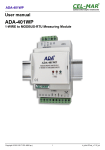
User manual
1MWUPRMDB001
Limitation of Liability
The Manufacturer reserves the right to modify the specifications in this manual without previous warning. Any copy of this manual, in
part or in full, whether by photocopy or by other means, even of electronic nature, without the manufacture giving written authorisation,
breaches the terms of copyright and is liable to prosecution.
It is absolutely forbidden to use the device for different uses other than those for which it has been devised for, as inferred to in this
manual. When using the features in this device, obey all laws and respect privacy and legitimate rights of others.
EXCEPT TO THE EXTENT PROHIBITED BY APPLICABLE LAW, UNDER NO CIRCUMSTANCES SHALL THE MANUFACTURER BE
LIABLE FOR CONSEQUENTIAL DAMAGES SUSTAINED IN CONNECTION WITH SAID PRODUCT AND THE MANUFACTURER NEITHER
ASSUMES NOR AUTHORIZES ANY REPRESENTATIVE OR OTHER PERSON TO ASSUME FOR IT ANY OBBLIGATION OR LIABILTY
OTHER THAN SUCH AS IS EXPRESSLY SET FORTH HEREIN.
All trademarks in this manual are property of their respective owners.
The information contained in this manual is for information purposes only, is subject to changes without previous warning and cannot
be considered binding for the Manufacturer. The Manufacturer assumes no responsabilty for any errors or incoherence possibly
contained in this manual.
MODBUS communication protocol
for WEZ Modbus and WEZ Ethernet modules
October edition 2013
Index
1. Description............................................................. 1
1.1 LRC generation...............................................................2
1.2 CRC generation...............................................................3
2. Read commands structure..................................... 6
2.1 MODBUS ASCII/RTU.......................................................6
2.2 MODBUS TCP..................................................................7
2.3 Floating point as per IEEE Standard...............................8
3. Write commands structure.................................... 9
3.1 MODBUS ASCII/RTU.......................................................9
3.2 MODBUS TCP................................................................10
4. Exception codes.................................................... 11
4.1 MODBUS ASCII/RTU.....................................................11
4.2 MODBUS TCP................................................................11
5. Register tables..................................................... 12
5.1 Reading registers (Function code $01 / $03 / $04).......13
5.2 Writing registers (Function code $10)..........................20
English
1. Description
MODBUS ASCII/RTU is a master-slave communication protocol, able to support up to 247 slaves connected in
a bus or a star network.
The protocol uses a simplex connection on a single line. In this way, the communication messages move on a
single line in two opposite directions.
MODBUS TCP is a variant of the MODBUS family. Specifically, it covers the use of MODBUS messaging in an
“Intranet” or “Internet” environment using the TCP/IP protocol on a fixed port 502.
Master-slave messages can be:
• Reading (Function code $01 / $03 / $04): the communication is between the master and a single slave.
It allows to read information about the queried counter
• Writing (Function code $10): the communication is between the master and a single slave. It allows to
change the counter settings
• Broadcast (not available for MODBUS TCP): the communication is between the master and all the
connected slaves. It is always a write command (Function code $10) and required logical number $00
In a multi-point type connection (MODBUS ASCII/RTU), slave address (called also logical number) allows to
identify each counter during the communication. Each counter is preset with a default slave address (01) and
the user can change it.
In case of MODBUS TCP, slave address is replaced by a single byte, the Unit identifier.
Communication frame structure
ASCII mode
Bit per byte: 1 Start, 7 Bit, Even, 1 Stop (7E1)
Name
Length
Function
START FRAME
1 char
Message start marker. Starts with colon “:” ($3A)
ADDRESS FIELD
2 chars
Counter logical number
FUNCTION CODE
2 chars
Function code ($01 / $03 / $04 / $10)
DATA FIELD
n chars
Data + length will be filled depending on the message type
ERROR CHECK
2 chars
Error check (LRC)
END FRAME
2 chars
Carriage return - line feed (CRLF) pair ($0D & $0A)
RTU mode
Bit per byte: 1 Start, 8 Bit, None, 1 Stop (8N1)
Name
Length
START FRAME
4 chars idle At least 4 character time of silence (MARK condition)
ADDRESS FIELD
8 bits
Counter logical number
FUNCTION CODE
8 bits
Function code ($01 / $03 / $04 / $10)
DATA FIELD
n x 8 bits
Data + length will be filled depending on the message type
ERROR CHECK
16 bits
Error check (CRC)
END FRAME
4 chars idle At least 4 character time of silence between frames
MODBUS RTU, ASCII, TCP
Function
1
English
TCP mode
Bit per byte: 1 Start, 7 Bit, Even, 2 Stop (7E2)
Name
Length
Function
TRANSACTION ID
2 bytes
For synchronization between messages of server & client
PROTOCOL ID
2 bytes
Zero for MODBUS TCP
BYTE COUNT
2 bytes
Number of remaining bytes in this frame
UNIT ID
1 byte
Slave address (255 if not used)
FUNCTION CODE
1 byte
Function code ($01 / $04 / $10)
DATA BYTES
n bytes
Data as response or command
1.1 LRC generation
The Longitudinal Redundancy Check (LRC) field is one byte, containing an 8–bit binary value. The LRC
value is calculated by the transmitting device, which appends the LRC to the message. The receiving
device recalculates an LRC during receipt of the message, and compares the calculated value to the
actual value it received in the LRC field. If the two values are not equal, an error results. The LRC is
calculated by adding together successive 8–bit bytes in the message, discarding any carries, and then
two’s complementing the result. The LRC is an 8–bit field, therefore each new addition of a character
that would result in a value higher than 255 decimal simply ‘rolls over’ the field’s value through zero.
Because there is no ninth bit, the carry is discarded automatically.
A procedure for generating an LRC is:
1. Add all bytes in the message, excluding the starting ‘colon’ and ending CR LF. Add them into an 8–bit
field, so that carries will be discarded.
2. Subtract the final field value from $FF, to produce the ones–complement.
3. Add 1 to produce the twos–complement.
Placing the LRC into the Message
When the the 8–bit LRC (2 ASCII characters) is transmitted in the message, the high–order character
will be transmitted first, followed by the low–order character. For example, if the LRC value is $52 (0101
0010):
Colon Addr
‘:’
Func
Data Data
Count
Data
….
Data
LRC
Hi ‘5’
LRC
Lo‘2’
CR
LF
C-function to calculate LRC
*pucFrame – pointer on “Addr” of message
usLen – length message from “Addr” to end “Data”
UCHAR prvucMBLRC( UCHAR * pucFrame, USHORT usLen )
{
UCHAR
ucLRC = 0; /* LRC char initialized */
while( usLen-- )
{
ucLRC += *pucFrame++;
}
/* Add buffer byte without carry */
/* Return twos complement */
ucLRC = ( UCHAR ) ( -( ( CHAR ) ucLRC ) );
return ucLRC;
}
2 MODBUS RTU, ASCII, TCP
The Cyclical Redundancy Check (CRC) field is two bytes, containing a 16–bit value. The CRC value is calculated
by the transmitting device, which appends the CRC to the message. The receiving device recalculates a CRC
during receipt of the message, and compares the calculated value to the actual value it received in the CRC
field. If the two values are not equal, an error results.
The CRC is started by first preloading a 16–bit register to all 1’s. Then a process begins of applying successive
8–bit bytes of the message to the current contents of the register. Only the eight bits of data in each character
are used for generating the CRC. Start and stop bits, and the parity bit, do not apply to the CRC.
During generation of the CRC, each 8–bit character is exclusive ORed with the register contents. Then the
result is shifted in the direction of the least significant bit (LSB), with a zero filled into the most significant bit
(MSB) position. The LSB is extracted and examined. If the LSB was a 1, the register is then exclusive ORed with
a preset, fixed value. If the LSB was a 0, no exclusive OR takes place.
This process is repeated until eight shifts have been performed. After the last (eighth) shift, the next 8–bit
character is exclusive ORed with the register’s current value, and the process repeats for eight more shifts as
described above. The final contents of the register, after all the characters of the message have been applied,
is the CRC value.
A calculated procedure for generating a CRC is:
1. Load a 16–bit register with $FFFF. Call this the CRC register.
2. Exclusive OR the first 8–bit byte of the message with the low–order byte of the 16–bit CRC register, putting
the result in the CRC register.
3. Shift the CRC register one bit to the right (toward the LSB), zero–filling the MSB. Extract and examine the
LSB.
4. (If the LSB was 0): Repeat Step 3 (another shift).
(If the LSB was 1): Exclusive OR the CRC register with the polynomial value $A001 (1010 0000 0000 0001).
5. Repeat Steps 3 and 4 until 8 shifts have been performed. When this is done, a complete 8–bit byte will have
been processed.
6. Repeat Steps 2 through 5 for the next 8–bit byte of the message. Continue doing this until all bytes have
been processed.
7. The final contents of the CRC register is the CRC value.
8. When the CRC is placed into the message, its upper and lower bytes must be swapped as described
below.
Placing the CRC into the Message
When the 16–bit CRC (two 8–bit bytes) is transmitted in the message, the low-order byte will be transmitted
first, followed by the high-order byte.
For example, if the CRC value is $35F7 (0011 0101 1111 0111):
Addr
MODBUS RTU, ASCII, TCP
Func
Data Data
Count
Data
….
Data
CRC
lo F7
CRC
hi 35
3
English
1.2 CRC generation
English
CRC generation functions - With Table
All of the possible CRC values are preloaded into two arrays, which are simply indexed as the function increments
through the message buffer. One array contains all of the 256 possible CRC values for the high byte of the 16–bit
CRC field, and the other array contains all of the values for the low byte. Indexing the CRC in this way provides
faster execution than would be achieved by calculating a new CRC value with each new character from the
message buffer.
/*CRC table for calculate with polynom 0xA001
rom unsigned char CRC_Table_Hi[] = {
0x00, 0xC1, 0x81, 0x40, 0x01, 0xC0, 0x80,
0x40, 0x01, 0xC0, 0x80, 0x41, 0x00, 0xC1,
0x80, 0x41, 0x01, 0xC0, 0x80, 0x41, 0x00,
0xC0, 0x80, 0x41, 0x00, 0xC1, 0x81, 0x40,
0x00, 0xC1, 0x81, 0x40, 0x01, 0xC0, 0x80,
0x40, 0x01, 0xC0, 0x80, 0x41, 0x00, 0xC1,
0x80, 0x41, 0x00, 0xC1, 0x81, 0x40, 0x00,
0xC0, 0x80, 0x41, 0x00, 0xC1, 0x81, 0x40,
0x00, 0xC1, 0x81, 0x40, 0x01, 0xC0, 0x80,
0x40, 0x00, 0xC1, 0x81, 0x40, 0x01, 0xC0,
0x80, 0x41, 0x01, 0xC0, 0x80, 0x41, 0x00,
0xC0, 0x80, 0x41, 0x01, 0xC0, 0x80, 0x41,
0x00, 0xC1, 0x81, 0x40, 0x00, 0xC1, 0x81,
0x40, 0x01, 0xC0, 0x80, 0x41, 0x01, 0xC0,
0x80, 0x41, 0x00, 0xC1, 0x81, 0x40, 0x00,
0xC0, 0x80, 0x41, 0x00, 0xC1, 0x81, 0x40,
0x00, 0xC1, 0x81, 0x40, 0x01, 0xC0, 0x80,
0x40
};
/*CRC table for calculate with polynom 0xA001
rom unsigned char CRC_Table_Lo[] = {
0x00, 0xC0, 0xC1, 0x01, 0xC3, 0x03, 0x02,
0x04, 0xCC, 0x0C, 0x0D, 0xCD, 0x0F, 0xCF,
0x08, 0xC8, 0xD8, 0x18, 0x19, 0xD9, 0x1B,
0x1D, 0x1C, 0xDC, 0x14, 0xD4, 0xD5, 0x15,
0x11, 0xD1, 0xD0, 0x10, 0xF0, 0x30, 0x31,
0x37, 0xF5, 0x35, 0x34, 0xF4, 0x3C, 0xFC,
0x3B, 0xFB, 0x39, 0xF9, 0xF8, 0x38, 0x28,
0x2E, 0x2F, 0xEF, 0x2D, 0xED, 0xEC, 0x2C,
0x22, 0xE2, 0xE3, 0x23, 0xE1, 0x21, 0x20,
0x62, 0x66, 0xA6, 0xA7, 0x67, 0xA5, 0x65,
0x6E, 0xAE, 0xAA, 0x6A, 0x6B, 0xAB, 0x69,
0x7B, 0x7A, 0xBA, 0xBE, 0x7E, 0x7F, 0xBF,
0x77, 0xB7, 0xB6, 0x76, 0x72, 0xB2, 0xB3,
0x51, 0x93, 0x53, 0x52, 0x92, 0x96, 0x56,
0x5D, 0x9D, 0x5F, 0x9F, 0x9E, 0x5E, 0x5A,
0x48, 0x49, 0x89, 0x4B, 0x8B, 0x8A, 0x4A,
0x44, 0x84, 0x85, 0x45, 0x87, 0x47, 0x46,
0x40
};
with init value 0xFFFF, High half word*/
0x41,
0x81,
0xC1,
0x01,
0x41,
0x81,
0xC1,
0x01,
0x41,
0x80,
0xC1,
0x00,
0x40,
0x80,
0xC1,
0x00,
0x41,
0x01,
0x40,
0x81,
0xC0,
0x00,
0x40,
0x81,
0xC0,
0x01,
0x41,
0x81,
0xC1,
0x01,
0x41,
0x81,
0xC1,
0x01,
0xC0,
0x00,
0x40,
0x80,
0xC1,
0x01,
0x40,
0x80,
0xC0,
0x00,
0x40,
0x81,
0xC0,
0x00,
0x40,
0x81,
0xC0,
0x80,
0xC1,
0x00,
0x41,
0x81,
0xC0,
0x01,
0x41,
0x80,
0xC1,
0x00,
0x40,
0x80,
0xC1,
0x01,
0x40,
0x80,
0x41,
0x81,
0xC1,
0x01,
0x40,
0x80,
0xC0,
0x00,
0x41,
0x81,
0xC1,
0x01,
0x41,
0x81,
0xC0,
0x01,
0x41,
0x00, 0xC1, 0x81,
0x40, 0x01, 0xC0,
0x81, 0x40, 0x01,
0xC0, 0x80, 0x41,
0x00, 0xC1, 0x81,
0x41, 0x01, 0xC0,
0x80, 0x41, 0x01,
0xC1, 0x81, 0x40,
0x00, 0xC1, 0x81,
0x40, 0x01, 0xC0,
0x81, 0x40, 0x01,
0xC0, 0x80, 0x41,
0x00, 0xC1, 0x81,
0x40, 0x01, 0xC0,
0x80, 0x41, 0x01,
0xC0, 0x80, 0x41,
0x00, 0xC1, 0x81,
with init value 0xFFFF, Low half word*/
0xC2,
0xCE,
0xDB,
0xD7,
0xF1,
0xFD,
0xE8,
0xE4,
0xE0,
0x64,
0xA9,
0x7D,
0x73,
0x57,
0x9A,
0x4E,
0x86,
0xC6,
0x0E,
0xDA,
0x17,
0x33,
0x3D,
0xE9,
0x24,
0xA0,
0xA4,
0xA8,
0xBD,
0xB1,
0x97,
0x9B,
0x8E,
0x82,
0x06,
0x0A,
0x1A,
0x16,
0xF3,
0xFF,
0x29,
0x25,
0x60,
0x6C,
0x68,
0xBC,
0x71,
0x55,
0x5B,
0x8F,
0x42,
0x07,
0xCA,
0x1E,
0xD6,
0xF2,
0x3F,
0xEB,
0xE5,
0x61,
0xAC,
0x78,
0x7C,
0x70,
0x95,
0x99,
0x4F,
0x43,
0xC7,
0xCB,
0xDE,
0xD2,
0x32,
0x3E,
0x2B,
0x27,
0xA1,
0xAD,
0xB8,
0xB4,
0xB0,
0x94,
0x59,
0x8D,
0x83,
0x05,
0x0B,
0xDF,
0x12,
0x36,
0xFE,
0x2A,
0xE7,
0x63,
0x6D,
0xB9,
0x74,
0x50,
0x54,
0x58,
0x4D,
0x41,
0xC5,
0xC9,
0x1F,
0x13,
0xF6,
0xFA,
0xEA,
0xE6,
0xA3,
0xAF,
0x79,
0x75,
0x90,
0x9C,
0x98,
0x4C,
0x81,
0xC4,
0x09,
0xDD,
0xD3,
0xF7,
0x3A,
0xEE,
0x26,
0xA2,
0x6F,
0xBB,
0xB5,
0x91,
0x5C,
0x88,
0x8C,
0x80,
unsigned short ModBus_CRC16( unsigned char * Buffer, unsigned short Length )
{
unsigned char CRCHi = 0xFF;
unsigned char CRCLo = 0xFF;
int
Index;
unsigned short ret;
while( Length-- )
{
Index = CRCLo ^ *Buffer++ ;
CRCLo = CRCHi ^ CRC_Table_Hi[Index];
CRCHi = CRC_Table_Lo[Index];
}
ret=((unsigned short)CRCHi << 8);
ret|= (unsigned short)CRCLo;
return ret;
}
4 MODBUS RTU, ASCII, TCP
English
CRC generation functions - Without Table
unsigned short ModBus_CRC16( unsigned char * Buffer, unsigned short Length )
{
/* ModBus_CRC16 Calculatd CRC16 with polynome 0xA001 and init value 0xFFFF
Input *Buffer - pointer on data
Input Lenght - number byte in buffer
Output - calculated CRC16
*/
unsigned int cur_crc;
cur_crc=0xFFFF;
do
{
unsigned int i = 8;
cur_crc = cur_crc ^ *Buffer++;
do
{
if (0x0001 & cur_crc)
{
cur_crc >>= 1;
cur_crc ^= 0xA001;
}
else
{
cur_crc >>= 1;
}
}
while (--i);
}
while (--Length);
return cur_crc;
}
MODBUS RTU, ASCII, TCP
5
English
2. Read commands structure
The master communication device can send commands to the module to read its status and setup or to read
the measured values, status and setup relevant to the counter.
More registers can be read, at the same time, sending a single command, only if the registers are consecutive
(see chapter 5).
According to the used MODBUS protocol mode, the read command is structured as follows.
2.1 MODBUS ASCII/RTU
Values contained both in Query or Response messages are in hex format.
Query example in case of MODBUS RTU: 01030002000265CB
Example
Byte
Description
No. of bytes
01
-
Slave address
1
03
-
Function code
1
00
High
02
Low
Starting register
2
00
High
02
Low
No. of words to be read
2
65
High
CB
Low
Error check (CRC)
2
Response example in case of MODBUS RTU: 01030400035571F547
6 Example
Byte
Description
No. of bytes
01
-
Slave address
1
03
-
Function code
1
04
-
Byte count
1
00
High
Requested data
4
Error check (CRC)
2
03
Low
55
High
71
Low
F5
High
47
Low
MODBUS RTU, ASCII, TCP
English
2.2 MODBUS TCP
Values contained both in Query or Response messages are in hex format.
Query example in case of MODBUS TCP: 010000000006010400020002
Example
Byte
01
-
00
High
00
Low
00
High
00
Low
06
01
Description
No. of bytes
Transaction identifier
1
Protocol identifier
4
-
Byte count
1
-
Unit identifier
1
04
-
Function code
1
00
High
02
Low
Starting register
2
00
High
02
Low
No. of words to be read
2
Response example in case of MODBUS TCP: 01000000000701040400035571
Example
Byte
01
-
00
High
00
Low
00
High
00
Low
07
Description
No. of bytes
Transaction identifier
1
Protocol identifier
4
-
Byte count
1
01
-
Unit identifier
1
04
-
Function code
1
04
-
No. of byte of requested data
2
00
High
03
Low
55
High
Requested data
4
71
Low
MODBUS RTU, ASCII, TCP
7
English
2.3 Floating point as per IEEE Standard
The basic format allows a IEEE standard floating-point number to be represented in a single 32 bit format, as
shown below:
N.n = (-1)S 2 e’-127 (1.f )
where S is the sign bit, e’ is the first part of the exponent and f is the decimal fraction placed next to 1. Internally
the exponent is 8 bits in length and the stored fraction is 23 bits long.
A round to nearest method is applied to the calculated value of floating point.
The floating-point format is shown as follows:
======================
| S | e + 127 |
f
|
======================
31
30
23 22
0 <—
bit number
where:
bit length
Sign
1
Exponent
8
Fraction
23 + (1)
Total
m = 32 + (1)
Exponent
Min e’
0
Max e’
255
Bias
127
NOTE
Fractions (decimals) are always shown while the leading 1 (hidden bit) is not stored.
Example of conversion of value shown with floating point
Value read with floating point:
45AACC00(16)
Value converted in binary format:
010001011 01010101100110000000000 (2)
exponent
fraction
sign
sign = 0
exponent = 10001011(2) = 139(10)
fraction = 01010101100110000000000(2) / 8388608 (10) =
= 2804736 (10) / 8388608 (10) = 0.334350585 (10)
N.n = (-1)S 2e’-127 (1+f ) =
= (-1)0 2139-127 (1.334350585)=
= (+1) (4096) (1.334350585) =
= 5465.5
8 MODBUS RTU, ASCII, TCP
English
3. Write commands structure
The master communication device can send commands to the module to program itself or to program the
counter.
More settings can be carried out, at the same time, sending a single command, only if the relevant registers
are consecutive (see chapter 5).
According to the used MODBUS protocol type, the write command is structured as follows.
3.1 MODBUS ASCII/RTU
Values contained both in Request or Response messages are in hex format.
Query example in case of MODBUS RTU: 011005150001020008F053
Example
Byte
Description
No. of bytes
01
-
Slave address
1
10
-
Function code
1
05
High
15
Low
Starting register
2
00
High
01
Low
No. of words to be written
2
02
-
Data byte counter
1
00
High
08
Low
Data for programming
2
F0
High
53
Low
Error check (CRC)
2
Response example in case of MODBUS RTU: 01100515000110C1
Example
Byte
Description
No. of bytes
01
-
Slave address
1
10
-
Function code
1
05
High
15
Low
Starting register
2
00
High
01
Low
No. of written words
2
10
High
C1
Low
Error check (CRC)
2
MODBUS RTU, ASCII, TCP
9
English
3.2 MODBUS TCP
Values contained both in Request or Response messages are in hex format.
Query example in case of MODBUS TCP: 010000000009011005150001020008
Example
Byte
01
-
00
High
00
Low
00
High
00
Low
09
01
Description
No. of bytes
Transaction identifier
1
Protocol identifier
4
-
Byte count
1
-
Unit identifier
1
10
-
Function code
1
05
High
15
Low
Starting register
2
00
High
01
Low
No. of words to be written
2
02
-
Data byte counter
1
00
High
08
Low
Data for programming
2
Response example in case of MODBUS TCP: 010000000006011005150001
10 Example
Byte
01
-
00
High
00
Low
00
High
00
Low
06
Description
No. of bytes
Transaction identifier
1
Protocol identifier
4
-
Byte count
1
01
-
Unit identifier
1
10
-
Function code
1
05
High
15
Low
Starting register
2
00
High
01
Low
Command successfully sent
2
MODBUS RTU, ASCII, TCP
English
4. Exception codes
When the module receives a not-valid query, an error message (exception code) is sent.
According to the used MODBUS protocol mode, possible exception codes are as follows.
4.1 MODBUS ASCII/RTU
Values contained in Response messages are in hex format.
Response example in case of MODBUS RTU: 01830131F0
Example
Byte
Description
No. of bytes
01
-
Slave address
1
83
-
Function code (80+03)
1
01
-
Exception code
1
31
High
F0
Low
Error check (CRC)
2
Exception codes for MODBUS ASCII/RTU are following described:
$01
ILLEGAL FUNCTION: the function code received in the query is not an allowable action.
$02
ILLEGAL DATA ADDRESS: the data address received in the query is not an allowable address (i.e.
the combination of register and transfer length is invalid).
$03
ILLEGAL DATA VALUE: a value contained in the query data field is not an allowable value.
$04
ILLEGAL RESPONSE LENGTH: the request would generate a response with size bigger than that
available for MODBUS protocol.
4.2 MODBUS TCP
Values contained in Response messages are in hex format.
Response example in case of MODBUS TCP: 010000000003018302
Example
Byte
01
-
00
High
Description
No. of bytes
Transaction identifier
1
Protocol identifier
4
00
Low
00
High
00
Low
03
-
No. of byte of next data in this string
1
01
-
Unit identifier
1
83
-
Function code (80+03)
1
02
-
Exception code
1
Exception codes for MODBUS TCP are following described:
$01
ILLEGAL FUNCTION: the function code is unknown by the server.
$02
ILLEGAL DATA ADDRESS: the data address received in the query is not an allowable address for
the counter (i.e. the combination of register and transfer length is invalid).
MODBUS RTU, ASCII, TCP
11
English
$03
ILLEGAL DATA VALUE: a value contained in the query data field is not an allowable value for the
counter.
$04
SERVER FAILURE: the server failed during the execution.
$05
ACKNOWLEDGE: the server accepted the server invocation but the service requires a relatively long
time to execute. The server therefore returns only an aknowledgement of the service invocation
receipt.
$06
SERVER BUSY: the server was unable to accept the MB request PDU. The client application has
the responsability of deciding if and when re-sending the request.
$0A
GATEWAY PATH UNAVAILABLE: the communication module is not configured or cannot
communicate.
$0B
GATEWAY TARGET DEVICE FAILED TO RESPOND: the counter is not available in the network.
5. Register tables
NOTE
Highest number of registers (or bytes) which can be read with a single command:
• in ASCII mode: 63 registers
• in RTU mode: 127 registers
• in TCP mode: 256 bytes
NOTE
Highest number of registers which can be programmed with a single command:
• in ASCII mode: 13 registers
• in RTU mode: 29 registers
• in TCP mode: 1 register
NOTE
The register values are in hex format ($).
Table HEADER
Meaning
Parameter
Measuring parameter to be read
Register description
Description of the register to be read / written
F. code (Hex)
Function code in hex format. It identifies the command type (reading / writing)
Sign
If this column is checked, the read register value can have positive or negative sign.
Convert a signed register value as shown in the following instructions:
The Most Significant Bit (MSB) indicates the sign as follows: 0=positive (+), 1=negative (-).
Negative value example:
12 MSB
$8020 = 1000000000100000 = -32
hexbindec
INTEGER
Details for INTEGER type registers
IEEE
Details for IEEE standard type registers
Register (Hex)
Register address in hex format
Words
Number of word to be read / written for the register (length)
M.U.
Measuring unit of parameter
Data meaning
Description of data received by a response of a reading command
Programmable data
Description of data which can be sent for a writing command
MODBUS RTU, ASCII, TCP
English
5.1 Reading registers (Function code $01 / $03 / $04)
F. code
(Hex)
Pa ra meter
INTE GE R
Sign
Register
Words
(Hex)
IE E E
M.U.
Register
Words
(Hex)
M.U.
Real time VALUES
V1 • L-N voltage phase 1
03 / 04
0000
2
mV
1000
2
V
V2 • L-N voltage phase 2
03 / 04
0002
2
mV
1002
2
V
V3 • L-N voltage phase 3
03 / 04
0004
2
mV
1004
2
V
V12 • L-L voltage line 12
03 / 04
0006
2
mV
1006
2
V
V23 • L-L voltage line 23
03 / 04
0008
2
mV
1008
2
V
V31 • L-L voltage line 31
03 / 04
000A
2
mV
100A
2
V
V∑ • System voltage
03 / 04
000C
2
mV
100C
2
V
A1 • Phase 1 current
03 / 04
X
000E
2
mA
100E
2
A
A2 • Phase 2 current
03 / 04
X
0010
2
mA
1010
2
A
A3 • Phase 3 current
03 / 04
X
0012
2
mA
1012
2
A
AN • Neutral current
03 / 04
X
0014
2
mA
1014
2
A
A∑ • System current
03 / 04
X
0016
2
mA
1016
2
A
PF1 • Phase 1 power factor
03 / 04
X
0018
1
-
1018
2
-
PF2 • Phase 2 power factor
03 / 04
X
0019
1
-
101A
2
-
PF3 • Phase 3 power factor
03 / 04
X
001A
1
-
101C
2
-
PF∑ • System power factor
03 / 04
X
001B
1
-
101E
2
-
P1 • Phase 1 active power
03 / 04
X
001C
3
mW
1020
2
W
P2 • Phase 2 active power
03 / 04
X
001F
3
mW
1022
2
W
P3 • Phase 3 active power
03 / 04
X
0022
3
mW
1024
2
W
P∑ • System active power
03 / 04
X
0025
3
mW
1026
2
W
S1 • Phase 1 apparent power
03 / 04
X
0028
3
mVA
1028
2
VA
S2 • Phase 2 apparent power
03 / 04
X
002B
3
mVA
102A
2
VA
S3 • Phase 3 apparent power
03 / 04
X
002E
3
mVA
102C
2
VA
S∑ • System apparent power
03 / 04
X
0031
3
mVA
102E
2
VA
Q1 • Phase 1 reactive power
03 / 04
X
0034
3
mvar
1030
2
var
Q2 • Phase 2 reactive power
03 / 04
X
0037
3
mvar
1032
2
var
Q3 • Phase 3 reactive power
03 / 04
X
003A
3
mvar
1034
2
var
Q∑ • System reactive power
03 / 04
X
003D
3
mvar
1036
2
var
F • Frequency
03 / 04
0040
1
mHz
1038
2
Hz
Phase sequence
03 / 04
0041
1
-
103A
2
-
+kWh1 • Phase 1 imported active energy
03 / 04
0100
3
0.1 Wh
1100
2
Wh
+kWh2 • Phase 2 imported active energy
03 / 04
0103
3
0.1 Wh
1102
2
Wh
+kWh3 • Phase 3 imported active energy
03 / 04
0106
3
0.1 Wh
1104
2
Wh
+kWh∑ • System imported active energy
03 / 04
0109
3
0.1 Wh
1106
2
Wh
-kWh1 • Phase 1 exported active energy
03 / 04
010C
3
0.1 Wh
1108
2
Wh
-kWh2 • Phase 2 exported active energy
03 / 04
010F
3
0.1 Wh
110A
2
Wh
-kWh3 • Phase 3 exported active energy
03 / 04
0112
3
0.1 Wh
110C
2
Wh
-kWh∑ • System exported active energy
03 / 04
0115
3
0.1 Wh
110E
2
Wh
+kVAh1-L • Phase 1 imported lagging apparent energy
03 / 04
0118
3
0.1 VAh
1110
2
VAh
+kVAh2-L • Phase 2 imported lagging apparent energy
03 / 04
011B
3
0.1 VAh
1112
2
VAh
+kVAh3-L • Phase 3 imported lagging apparent energy
03 / 04
011E
3
0.1 VAh
1114
2
VAh
+kVAh∑-L • System imported lagging apparent energy
03 / 04
0121
3
0.1 VAh
1116
2
VAh
$00=123-CCW, $01=321-CW, $02=not available (in case of 1-phase counter)
total counter values
MODBUS RTU, ASCII, TCP
13
English
Pa ra meter
F. code
(Hex)
INTE GE R
Sign
Register
Words
(Hex)
IE E E
M.U.
Register
Words
(Hex)
M.U.
total counter values
-kVAh1-L • Phase 1 exported lagging apparent energy
03 / 04
0124
3
0.1 VAh
1118
2
VAh
-kVAh2-L • Phase 2 exported lagging apparent energy
-kVAh3-L • Phase 3 exported lagging apparent energy
03 / 04
0127
3
03 / 04
012A
3
0.1 VAh
111A
2
VAh
0.1 VAh
111C
2
VAh
-kVAh∑-L • System exported lagging apparent energy
03 / 04
012D
3
0.1 VAh
111E
2
VAh
+kVAh1-C • Phase 1 imported leading apparent energy
03 / 04
0130
3
0.1 VAh
1120
2
VAh
+kVAh2-C • Phase 2 imported leading apparent energy
03 / 04
0133
3
0.1 VAh
1122
2
VAh
+kVAh3-C • Phase 3 imported leading apparent energy
03 / 04
0136
3
0.1 VAh
1124
2
VAh
+kVAh∑-C • System imported leading apparent energy
03 / 04
0139
3
0.1 VAh
1126
2
VAh
-kVAh1-C • Phase 1 exported leading apparent energy
03 / 04
013C
3
0.1 VAh
1128
2
VAh
-kVAh2-C • Phase 2 exported leading apparent energy
03 / 04
013F
3
0.1 VAh
112A
2
VAh
-kVAh3-C • Phase 3 exported leading apparent energy
03 / 04
0142
3
0.1 VAh
112C
2
VAh
-kVAh∑-C • System exported leading apparent energy
03 / 04
0145
3
0.1 VAh
112E
2
VAh
+kvarh1-L • Phase 1 imported lagging reactive energy
03 / 04
0148
3
0.1 varh
1130
2
varh
+kvarh2-L • Phase 2 imported lagging reactive energy
03 / 04
014B
3
0.1 varh
1132
2
varh
+kvarh3-L • Phase 3 imported lagging reactive energy
03 / 04
014E
3
0.1 varh
1134
2
varh
+kvarh∑-L • System imported lagging reactive energy
03 / 04
0151
3
0.1 varh
1136
2
varh
-kvarh1-L • Phase 1 exported lagging reactive energy
03 / 04
0154
3
0.1 varh
1138
2
varh
-kvarh2-L • Phase 2 exported lagging reactive energy
03 / 04
0157
3
0.1 varh
113A
2
varh
-kvarh3-L • Phase 3 exported lagging reactive energy
03 / 04
015A
3
0.1 varh
113C
2
varh
-kvarh∑-L • System exported lagging reactive energy
03 / 04
015D
3
0.1 varh
113E
2
varh
+kvarh1-C • Phase 1 imported leading reactive energy
03 / 04
0160
3
0.1 varh
1140
2
varh
+kvarh2-C • Phase 2 imported leading reactive energy
03 / 04
0163
3
0.1 varh
1142
2
varh
+kvarh3-C • Phase 3 imported leading reactive energy
03 / 04
0166
3
0.1 varh
1144
2
varh
+kvarh∑-C • System imported leading reactive energy
03 / 04
0169
3
0.1 varh
1146
2
varh
-kvarh1-C • Phase 1 exported leading reactive energy
03 / 04
016C
3
0.1 varh
1148
2
varh
-kvarh2-C • Phase 2 exported leading reactive energy
03 / 04
016F
3
0.1 varh
114A
2
varh
-kvarh3-C • Phase 3 exported leading reactive energy
03 / 04
0172
3
0.1 varh
114C
2
varh
-kvarh∑-C • System exported leading reactive energy
03 / 04
0175
3
0.1 varh
114E
2
varh
+kWh1 • Phase 1 imported active energy
03 / 04
0200
3
0.1 Wh
1200
2
Wh
+kWh2 • Phase 2 imported active energy
03 / 04
0203
3
0.1 Wh
1202
2
Wh
+kWh3 • Phase 3 imported active energy
03 / 04
0206
3
0.1 Wh
1204
2
Wh
+kWh∑ • System imported active energy
03 / 04
0209
3
0.1 Wh
1206
2
Wh
-kWh1 • Phase 1 exported active energy
03 / 04
020C
3
0.1 Wh
1208
2
Wh
-kWh2 • Phase 2 exported active energy
03 / 04
020F
3
0.1 Wh
120A
2
Wh
-kWh3 • Phase 3 exported active energy
03 / 04
0212
3
0.1 Wh
120C
2
Wh
-kWh∑ • System exported active energy
03 / 04
0215
3
0.1 Wh
120E
2
Wh
+kVAh1-L • Phase 1 imported lagging apparent energy
03 / 04
0218
3
0.1 VAh
1210
2
VAh
+kVAh2-L • Phase 2 imported lagging apparent energy
03 / 04
021B
3
0.1 VAh
1212
2
VAh
+kVAh3-L • Phase 3 imported lagging apparent energy
03 / 04
021E
3
0.1 VAh
1214
2
VAh
+kVAh∑-L • System imported lagging apparent energy
03 / 04
0221
3
0.1 VAh
1216
2
VAh
-kVAh1-L • Phase 1 exported lagging apparent energy
03 / 04
0224
3
0.1 VAh
1218
2
VAh
-kVAh2-L • Phase 2 exported lagging apparent energy
03 / 04
0227
3
0.1 VAh
121A
2
VAh
-kVAh3-L • Phase 3 exported lagging apparent energy
03 / 04
022A
3
0.1 VAh
121C
2
VAh
-kVAh∑-L • System exported lagging apparent energy
03 / 04
022D
3
0.1 VAh
121E
2
VAh
+kVAh1-C • Phase 1 imported leading apparent energy
03 / 04
0230
3
0.1 VAh
1220
2
VAh
tARIFF 1 counter values
14 MODBUS RTU, ASCII, TCP
Pa ra meter
INTE GE R
Sign
Register
Words
(Hex)
IE E E
M.U.
Register
Words
(Hex)
M.U.
tARIFF 1 counter values
+kVAh2-C • Phase 2 imported leading apparent energy
03 / 04
0233
3
0.1 VAh
1222
2
VAh
+kVAh3-C • Phase 3 imported leading apparent energy
03 / 04
0236
3
0.1 VAh
1224
2
VAh
+kVAh∑-C • System imported leading apparent energy
03 / 04
0239
3
0.1 VAh
1226
2
VAh
-kVAh1-C • Phase 1 exported leading apparent energy
03 / 04
023C
3
0.1 VAh
1228
2
VAh
-kVAh2-C • Phase 2 exported leading apparent energy
03 / 04
023F
3
0.1 VAh
122A
2
VAh
-kVAh3-C • Phase 3 exported leading apparent energy
03 / 04
0242
3
0.1 VAh
122C
2
VAh
-kVAh∑-C • System exported leading apparent energy
03 / 04
0245
3
0.1 VAh
122E
2
VAh
+kvarh1-L • Phase 1 imported lagging reactive energy
03 / 04
0248
3
0.1 varh
1230
2
varh
+kvarh2-L • Phase 2 imported lagging reactive energy
03 / 04
024B
3
0.1 varh
1232
2
varh
+kvarh3-L • Phase 3 imported lagging reactive energy
03 / 04
024E
3
0.1 varh
1234
2
varh
+kvarh∑-L • System imported lagging reactive energy
03 / 04
0251
3
0.1 varh
1236
2
varh
-kvarh1-L • Phase 1 exported lagging reactive energy
03 / 04
0254
3
0.1 varh
1238
2
varh
-kvarh2-L • Phase 2 exported lagging reactive energy
03 / 04
0257
3
0.1 varh
123A
2
varh
-kvarh3-L • Phase 3 exported lagging reactive energy
03 / 04
025A
3
0.1 varh
123C
2
varh
-kvarh∑-L • System exported lagging reactive energy
03 / 04
025D
3
0.1 varh
123E
2
varh
+kvarh1-C • Phase 1 imported leading reactive energy
03 / 04
0260
3
0.1 varh
1240
2
varh
+kvarh2-C • Phase 2 imported leading reactive energy
03 / 04
0263
3
0.1 varh
1242
2
varh
+kvarh3-C • Phase 3 imported leading reactive energy
03 / 04
0266
3
0.1 varh
1244
2
varh
+kvarh∑-C • System imported leading reactive energy
03 / 04
0269
3
0.1 varh
1246
2
varh
-kvarh1-C • Phase 1 exported leading reactive energy
03 / 04
026C
3
0.1 varh
1248
2
varh
-kvarh2-C • Phase 2 exported leading reactive energy
03 / 04
026F
3
0.1 varh
124A
2
varh
-kvarh3-C • Phase 3 exported leading reactive energy
03 / 04
0272
3
0.1 varh
124C
2
varh
-kvarh∑-C • System exported leading reactive energy
03 / 04
0275
3
0.1 varh
124E
2
varh
+kWh1 • Phase 1 imported active energy
03 / 04
0300
3
0.1 Wh
1300
2
Wh
+kWh2 • Phase 2 imported active energy
03 / 04
0303
3
0.1 Wh
1302
2
Wh
+kWh3 • Phase 3 imported active energy
03 / 04
0306
3
0.1 Wh
1304
2
Wh
+kWh∑ • System imported active energy
03 / 04
0309
3
0.1 Wh
1306
2
Wh
-kWh1 • Phase 1 exported active energy
03 / 04
030C
3
0.1 Wh
1308
2
Wh
-kWh2 • Phase 2 exported active energy
03 / 04
030F
3
0.1 Wh
130A
2
Wh
-kWh3 • Phase 3 exported active energy
03 / 04
0312
3
0.1 Wh
130C
2
Wh
-kWh∑ • System exported active energy
03 / 04
0315
3
0.1 Wh
130E
2
Wh
+kVAh1-L • Phase 1 imported lagging apparent energy
03 / 04
0318
3
0.1 VAh
1310
2
VAh
+kVAh2-L • Phase 2 imported lagging apparent energy
03 / 04
031B
3
0.1 VAh
1312
2
VAh
+kVAh3-L • Phase 3 imported lagging apparent energy
03 / 04
031E
3
0.1 VAh
1314
2
VAh
+kVAh∑-L • System imported lagging apparent energy
03 / 04
0321
3
0.1 VAh
1316
2
VAh
-kVAh1-L • Phase 1 exported lagging apparent energy
03 / 04
0324
3
0.1 VAh
1318
2
VAh
-kVAh2-L • Phase 2 exported lagging apparent energy
03 / 04
0327
3
0.1 VAh
131A
2
VAh
-kVAh3-L • Phase 3 exported lagging apparent energy
03 / 04
032A
3
0.1 VAh
131C
2
VAh
-kVAh∑-L • System exported lagging apparent energy
03 / 04
032D
3
0.1 VAh
131E
2
VAh
+kVAh1-C • Phase 1 imported leading apparent energy
03 / 04
0330
3
0.1 VAh
1320
2
VAh
+kVAh2-C • Phase 2 imported leading apparent energy
03 / 04
0333
3
0.1 VAh
1322
2
VAh
+kVAh3-C • Phase 3 imported leading apparent energy
03 / 04
0336
3
0.1 VAh
1324
2
VAh
+kVAh∑-C • System imported leading apparent energy
03 / 04
0339
3
0.1 VAh
1326
2
VAh
-kVAh1-C • Phase 1 exported leading apparent energy
03 / 04
033C
3
0.1 VAh
1328
2
VAh
-kVAh2-C • Phase 2 exported leading apparent energy
03 / 04
033F
3
0.1 VAh
132A
2
VAh
tARIFF 2 counter values
MODBUS RTU, ASCII, TCP
15
English
F. code
(Hex)
English
Pa ra meter
F. code
(Hex)
INTE GE R
Sign
Register
Words
(Hex)
IE E E
M.U.
Register
Words
(Hex)
M.U.
tARIFF 2 counter values
-kVAh3-C • Phase 3 exported leading apparent energy
03 / 04
0342
3
0.1 VAh
132C
2
-kVAh∑-C • System exported leading apparent energy
03 / 04
0345
+kvarh1-L • Phase 1 imported lagging reactive energy
03 / 04
0348
+kvarh2-L • Phase 2 imported lagging reactive energy
03 / 04
+kvarh3-L • Phase 3 imported lagging reactive energy
VAh
3
0.1 VAh
132E
2
VAh
3
0.1 varh
1330
2
varh
034B
3
0.1 varh
1332
2
varh
03 / 04
034E
3
0.1 varh
1334
2
varh
+kvarh∑-L • System imported lagging reactive energy
03 / 04
0351
3
0.1 varh
1336
2
varh
-kvarh1-L • Phase 1 exported lagging reactive energy
03 / 04
0354
3
0.1 varh
1338
2
varh
-kvarh2-L • Phase 2 exported lagging reactive energy
03 / 04
0357
3
0.1 varh
133A
2
varh
-kvarh3-L • Phase 3 exported lagging reactive energy
03 / 04
035A
3
0.1 varh
133C
2
varh
-kvarh∑-L • System exported lagging reactive energy
03 / 04
035D
3
0.1 varh
133E
2
varh
+kvarh1-C • Phase 1 imported leading reactive energy
03 / 04
0360
3
0.1 varh
1340
2
varh
+kvarh2-C • Phase 2 imported leading reactive energy
03 / 04
0363
3
0.1 varh
1342
2
varh
+kvarh3-C • Phase 3 imported leading reactive energy
03 / 04
0366
3
0.1 varh
1344
2
varh
+kvarh∑-C • System imported leading reactive energy
03 / 04
0369
3
0.1 varh
1346
2
varh
-kvarh1-C • Phase 1 exported leading reactive energy
03 / 04
036C
3
0.1 varh
1348
2
varh
-kvarh2-C • Phase 2 exported leading reactive energy
03 / 04
036F
3
0.1 varh
134A
2
varh
-kvarh3-C • Phase 3 exported leading reactive energy
03 / 04
0372
3
0.1 varh
134C
2
varh
-kvarh∑-C • System exported leading reactive energy
03 / 04
0375
3
0.1 varh
134E
2
varh
+kWh∑ • System imported active energy
03 / 04
0400
3
0.1 Wh
1400
2
Wh
-kWh∑ • System exported active energy
03 / 04
0403
3
0.1 Wh
1402
2
Wh
+kVAh∑-L • System imported lagging apparent energy
03 / 04
0406
3
0.1 VAh
1404
2
VAh
-kVAh∑-L • System exported lagging apparent energy
03 / 04
0409
3
0.1 VAh
1406
2
VAh
+kVAh∑-C • System imported leading apparent energy
03 / 04
040C
3
0.1 VAh
1408
2
VAh
-kVAh∑-C • System exported leading apparent energy
03 / 04
040F
3
0.1 VAh
140A
2
VAh
+kvarh∑-L • System imported lagging reactive energy
03 / 04
0412
3
0.1 varh
140C
2
varh
-kvarh∑-L • System exported lagging reactive energy
03 / 04
0415
3
0.1 varh
140E
2
varh
+kvarh∑-C • System imported leading reactive energy
03 / 04
0418
3
0.1 varh
1410
2
varh
-kvarh∑-C • System exported leading reactive energy
03 / 04
041B
3
0.1 varh
1412
2
varh
PARTIAL counter values
BALANCE values
kWh∑ • System active energy
03 / 04
X
041E
3
0.1 Wh
1414
2
Wh
kVAh∑-L • System lagging apparent energy
03 / 04
X
0421
3
0.1 VAh
1416
2
VAh
kVAh∑-C • System leading apparent energy
03 / 04
X
0424
3
0.1 VAh
1418
2
VAh
kvarh∑-L • System lagging reactive energy
03 / 04
X
0427
3
0.1 varh
141A
2
varh
kvarh∑-C • System leading reactive energy
03 / 04
X
042A
3
0.1 varh
141C
2
varh
16 MODBUS RTU, ASCII, TCP
English
R eg is ter des c r i pti o n
F. code
(Hex)
INTE GE R
D a ta mea n ing
Register
Words
(Hex)
COUNTEr & COMMUNICATION data
Serial number
03 / 04
0500
5
10 ASCII chars. ($00÷$FF)
Model
03 / 04
0505
1
$03=6A 3phases/4wires
$06=6A 3phases/3wires
$08=80A 3phases/4wires
$0A=80A 3phases/3wires
$0C=80A 1phase/2wires
Type
03 / 04
0506
1
$01=NO MID
$02=MID
Firmware release
03 / 04
0507
1
Convert the read Hex value in
Decimal value.
e.g. $66=102
=rel. 1.02
Hardware version
03 / 04
0508
1
Convert the read Hex value in
Decimal value.
e.g. $64=100
=rev. 1.00
Reserved
03 / 04
0509
2
Tariff in use
03 / 04
050B
1
$01=tariff 1
$02=tariff 2
Primary/secondary value
03 / 04
050C
1
$00=primary
$01=secondary
Error code
03 / 04
050D
1
$00=none
$01=phase sequence error
CT value (only for counter 6A 3phase model)
03 / 04
050E
1
$0001÷$2710
Reserved
03 / 04
050F
2
FSA value
03 / 04
0511
1
$00=1A
$01=5A
$02=80A
Wiring mode
03
0512
1
$01=3phases/4-wires
$02=3phases/3-wires
$03=1-phase
$04=3phases/2-wires
MODBUS address
(not available for MODBUS TCP)
03
0513
1
$01÷$F7
MODBUS mode
(not available for MODBUS TCP)
03
0514
1
$00=7E2 (ASCII)
$01=8N1 (RTU)
Communication speed
(not available for MODBUS TCP)
03
0515
1
$01=300 bps
$02=600 bps
$03=1200 bps
$04=2400 bps
$05=4800 bps
$06=9600 bps
$07=19200 bps
$08=38400 bps
$09=57600 bps
MODBUS RTU, ASCII, TCP
17
English
R eg is ter des c r i pti o n
F. code
(Hex)
INTE GE R
Register
Words
(Hex)
D a ta mea n ing
COUNTEr & COMMUNICATION data
Partial counters status
03
0517
1
Convert the read Hex value in
Binary.
e.g. $0003=
0000000000000011
Each bit corresponds to the status
of a partial counter.
0=inactive
1=active
0000000000000011
<
Start to read bit string following
the arrow. The first bit corresponds
to the status of the first counter in
the list:
1)+kWh∑ PAR
2)-kWh∑ PAR
3)+kVAh∑-L PAR
4)-kVAh∑-L PAR
5)+kVAh∑-C PAR
6)-kVAh∑-C PAR
7)+kvarh∑-L PAR
8)-kvarh∑-L PAR
9)+kvarh∑-C PAR
10)-kvarh∑-C PAR
The last six bits of the string are
reserved.
In the example, only +kWh∑ PAR
and -kWh∑ PAR counters are
active.
COMMUNICATION MODULE data
Serial number
03 / 04
0518
5
Reserved
03 / 04
051D
2
Firmware release
03 / 04
051F
1
Convert the read Hex value in
Decimal value.
e.g. $66=102
=rel. 1.02
Hardware version
03 / 04
0520
1
Convert the read Hex value in
Decimal value.
e.g. $64=100
=rev. 1.00
18 10 ASCII chars. ($00÷$FF)
MODBUS RTU, ASCII, TCP
F. code
(Hex)
Register
(Hex)
01
0000
English
R eg is ter des c r i pti o n
D a ta mea n in g
COILS
Alarm events
40 coils
Byte 1 - voltage out of range
|UV3|UV2|UV1|UV∑| OV3 | OV2 | OV1 |OV∑ |
Byte 2 - line voltage out of range
|COM|RES|UV23| UV31| UV12| OV23| OV31| OV12|
Byte 3/4 - current out of range
|R ES|RES|RES|RES|RES|RES|UIN| UI3 |
|U I 2 |U I 1 |U I ∑ |O I N |O I 3 |O I 2 |O I 1 |O I ∑ |
Byte 5 - frequency out of range
|R ES|RES|RES|RES|RES|RES|RES| F |
LEGEND
UV=undervoltage
OV=overvoltage
UI=undercurrent
OI=overcurrent
F=frequency out of range
COM=communication in progress
RES=reserved bit to 0
NOTE: the voltage, current and frequency
threshold values can change according to
the counter model. Please refer to the table
shown below.
PARAMETER THRESHOLDS
COUNTER
NOMINAL
VOLTAGE
PHASE VOLTAGE
available only for 2-4
wire model counters
A
B
C
D
MODBUS RTU, ASCII, TCP
LINE VOLTAGE
not available for
2 wire model counter
UVL-N: Vnom -20%
OVL-N: Vnom +20%
UVL-L: Vnom * √3 -20%
OVL-L: Vnom * √3 +20%
UVL-N: 230V -20%
OVL-N: 240V +20%
UVL-L: 400V -20%
OVL-L: 415V +20%
CUrrent
UI: Start current value (Ist)
OI: Full scale value (FS)
FrequenCY
F low: 45Hz
F high: 65Hz
19
English
5.2 Writing registers (Function code $10)
R eg is ter des c r i pti o n
F. code
(Hex)
INTE GE R
Register
Words
(Hex)
P rogra mma ble data
COUNTEr & COMMUNICATION data
MODBUS address
(not available for MODBUS TCP)
10
0513
1
$01÷$F7
MODBUS mode
(not available for MODBUS TCP)
10
0514
1
$00=7E2 (ASCII)
$01=8N1 (RTU)
Communication speed
(not available for MODBUS TCP)
10
0515
1
$01=300 bps
$02=600 bps
$03=1200 bps
$04=2400 bps
$05=4800 bps
$06=9600 bps
$07=19200 bps
$08=38400 bps
$09=57600 bps
Reserved
10
0516
1
Partial counters status
10
0517
1
Byte 1 - partial counter selection:
$00=+kWh∑ PAR
$01=-kWh∑ PAR
$02=+kVAh∑-L PAR
$03=-kVAh∑-L PAR
$04=+kVAh∑-C PAR
$05=-kVAh∑-C PAR
$06=+kvarh∑-L PAR
$07=-kvarh∑-L PAR
$08=+kvarh∑-C PAR
$09=-kvarh∑-C PAR
$0A=all partial counters
Byte 2 - partial counter/s operation:
$01=start
$02=stop
$03=reset
e.g. start +kWh∑ PAR counter
00=+kWh∑ PAR
01=start
final value to be set: 0001
NOTE
$0513, $0514, $0515 writing registers allow to program the communication parameters.
20 MODBUS RTU, ASCII, TCP
English
MODBUS RTU, ASCII, TCP
21
Erlenstraße 14 • 90441 Nürnberg • GERMANY
Tel. : +49 (0)911 / 4 23 47 - 0 • Fax : +49 (0)911 / 4 23 47 - 39
[email protected] • www.weigel-messgeraete.de