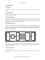
1
DIO24 PCI-DIO24 PMC-DIO24 PCI-DIO24-GD1 User Manual Manual Revision: June 12, 2002 General Standards Corporation 8302A Whitesburg Drive Huntsville, AL 35802 Phone: (256) 880-8787 Fax: (256) 880-8788 URL: www.generalstandards.com E-mail: [email protected] E-mail: [email protected] DIO24, User Manual 2 General Standards Corporation, Phone: (256) 880-8787 DIO24, User Manual Preface Copyright ©2002, General Standards Corporation Additional copies of this manual or other literature may be obtained from: General Standards Corporation 8302A Whitesburg Dr. Huntsville, Alabama 35802 Phone: (256) 880-8787 FAX: (256) 880-8788 URL: www.generalstandards.com E-mail: [email protected] General Standards Corporation makes no warranty of any kind with regard to this material, including, but not limited to, the implied warranties of merchantability and fitness for a particular purpose. Although extensive editing and reviews are performed before release to ECO control, General Standards Corporation assumes no responsibility for any errors that may exist in this document. No commitment is made to update or keep current the information contained in this document. General Standards Corporation does not assume any liability arising out of the application or use of any product or circuit described herein, nor is any license conveyed under any patent rights or any rights of others. General Standards Corporation assumes no responsibility for any consequences resulting from omissions or errors in this manual or from the use of information contained herein. General Standards Corporation reserves the right to make any changes, without notice, to this product to improve reliability, performance, function, or design. ALL RIGHTS RESERVED. The information in this document is subject to change without notice. This document may be copied or reproduced provided it is in support of products from General Standards Corporation. For any other use, no part of this document may be copied or reproduced in any form or by any means without prior written consent of General Standards Corporation. GSC is a trademark of General Standards Corporation. PLX and PLX Technology are trademarks of PLX Technology, Inc. 3 General Standards Corporation, Phone: (256) 880-8787 DIO24, User Manual Table of Contents 1. Introduction............................................................................................................................... 7 1.1. Purpose ...............................................................................................................................................................7 1.2. Plug and Play ......................................................................................................................................................7 1.3. System Resources ...............................................................................................................................................7 1.4. Hardware Overview ............................................................................................................................................7 1.4.1. HOST Interface ............................................................................................................................................7 1.4.2. External I/O Interface ...................................................................................................................................7 1.5. Ordering Information ..........................................................................................................................................8 1.6. Custom Applications...........................................................................................................................................8 1.7. Reference Material..............................................................................................................................................8 2. Physical Description................................................................................................................ 10 2.1. Identification.....................................................................................................................................................10 2.1.1. PCI-DIO24 .................................................................................................................................................10 2.1.2. PCI-DIO24-GD1 ........................................................................................................................................11 2.2. Connectors ........................................................................................................................................................11 2.2.1. External I/O Connection: P1.......................................................................................................................11 2.3. Jumpers .............................................................................................................................................................12 2.3.1. Jumper Block: J2 ........................................................................................................................................12 2.4. Components ......................................................................................................................................................13 2.4.1. FPGA EPROM: U42 ..................................................................................................................................13 2.4.2. Termination Resistors: RP1 – RP7 .............................................................................................................13 2.5. Cables ...............................................................................................................................................................14 2.5.1. Loop Back Test Cable ................................................................................................................................14 3. Operation ................................................................................................................................. 15 3.1. Identification.....................................................................................................................................................15 3.2. Reset .................................................................................................................................................................15 3.3. I/O Programming ..............................................................................................................................................15 3.4. I/O Reads and Writes ........................................................................................................................................15 4. Registers................................................................................................................................... 16 4.1. PCI Configuration Registers .............................................................................................................................16 4.2. PLX PCI9080 Internal Registers.......................................................................................................................16 4.3. GSC Specific Registers.....................................................................................................................................16 4.3.1. Firmware Revision Register (FRR, 0x00, 32, RO).....................................................................................16 4.3.2. Board Control Register (BCR, 0x04, 32, RW) ...........................................................................................17 4.3.3. Board Status Register (BSR, 0x08, 32, RO)...............................................................................................17 4.3.4. I/O Control Register (IOCR, 0x60, 32, RW)..............................................................................................18 4.3.5. Discrete Data Output Register (DDOR, 0x64, 32, RW).............................................................................18 4.3.6. Discrete Data Input Register (DDIR, 0x68, 32, RO)..................................................................................18 4 General Standards Corporation, Phone: (256) 880-8787 DIO24, User Manual 5. PLX PCI9080 Registers.......................................................................................................... 20 5.1. PCI Configuration Registers .............................................................................................................................20 5.1.1. PCI Configuration ID Register ...................................................................................................................20 5.1.2. PCI Command Register ..............................................................................................................................20 5.1.3. PCI Status Register.....................................................................................................................................21 5.1.4. PCI Revision ID Register ...........................................................................................................................22 5.1.5. PCI Class Code Register.............................................................................................................................22 5.1.6. PCI Cache Line Size Register ....................................................................................................................22 5.1.7. PCI Latency Timer Register .......................................................................................................................22 5.1.8. PCI Header Type Register..........................................................................................................................22 5.1.9. PCI Base Address Register for Memory Access to Local/Runtime/DMA Registers .................................22 5.1.10. PCI Base Address Register for I/O Access to Local/Runtime/DMA Registers........................................23 5.1.11. PCI Base Address Register for Memory Access to Local Address Space 0.............................................23 5.1.12. PCI Subsystem Device/Vendor ID Register.............................................................................................23 5.1.13. PCI Interrupt Line Register ......................................................................................................................23 5.1.14. PCI Interrupt Pin Register ........................................................................................................................23 5.1.15. PCI Min_Gnt Register ..............................................................................................................................24 5.1.16. PCI Max_Lat Register ..............................................................................................................................24 5.2. Local Configuration Registers ..........................................................................................................................24 5.2.1. Local Address Space 0 Range Register for PCI to Local Bus ....................................................................24 5.2.2. Mode/Arbitration Register..........................................................................................................................25 5.2.3. Big/Little Endian Descriptor Register ........................................................................................................25 5.2.4. Local Address Space 0/Expansion ROM Bus Region Descriptor Register ................................................25 5.3. Runtime Registers.............................................................................................................................................26 5.3.1. Interrupt Control /Status .............................................................................................................................26 5.3.2. Serial EEPROM Control, PCI Command Codes, User I/O Control, Init Control Register ........................27 5.3.3. PCI Permanent Configuration ID Register .................................................................................................27 5.3.4. PCI Permanent Revision ID Register .........................................................................................................27 5.4. DMA Registers .................................................................................................................................................28 5.5. Messaging Queue Registers ..............................................................................................................................28 Document History ....................................................................................................................... 29 5 General Standards Corporation, Phone: (256) 880-8787 DIO24, User Manual Table of Figures Figure 1 DIO24 simple block diagram. .........................................................................................................................7 Figure 2 An illustration of a PCI-DIO24. ....................................................................................................................10 Figure 3 External I/O connector P1. ............................................................................................................................11 Figure 4 Jumper block J2.............................................................................................................................................12 Table of Tables Table 1 Register level identification of the DIO24......................................................................................................10 Table 2 Register level identification of the PCI-DIO24-GD1. ....................................................................................11 Table 3 External I/O connector P1 pins and descriptions............................................................................................11 Table 4 Register level identification of the DIO24......................................................................................................15 Table 5 Register map of the GSC specific registers. ...................................................................................................16 Table 6 Register map of the PCI Configuration Registers...........................................................................................20 Table 7 Register map of the Local Configuration Registers........................................................................................24 Table 8 Register map of the Runtime Registers. .........................................................................................................26 6 General Standards Corporation, Phone: (256) 880-8787 DIO24, User Manual 1. Introduction 1.1. Purpose The purpose of this document is to briefly describe the DIO24 I/O board, its features, its use and its hardware interface. 1.2. Plug and Play The DIO24 is Plug and Play compatible. If the host is also Plug and Play compatible then the BIOS will recognize and configure the DIO24 accordingly. 1.3. System Resources Through Plug and Play initialization, the DIO24 is given three system resources. This includes a 256-byte block of memory space for the PLX PCI9080 feature set registers, plus an identical block for the same registers that is mapped to I/O port space. It also includes a 512-byte block of memory for the GSC specific DIO24 registers. This board requires neither a DMA channel nor an interrupt request line. 1.4. Hardware Overview The DIO24 is a simple 25-bit discrete I/O interface board. The host side connection is PCI based and the external I/O interface is variable (see below). The external interface includes 24 pins that can be arbitrarily programmed as either input or output and one pin that is input only. The 24 programmable pins are divided into three groups of eight pins each; Port A, Port B and Port C. Ports A and B are each programmable as all inputs or all outputs. The Port C pins are individually programmable. Figure 1 DIO24 simple block diagram. Port A (8 bits) PCI Interface DIO24 Internal Logic PLX PCI9080 Port B (8 bits) Port C (8 bits) Transcievers Cable Interface Dedicated Input (1 bit) or clock output 1.4.1. HOST Interface The PCI interface on the DIO24 is implemented using the PCI9080 from PLX Technology. The PCI interface is compliant with the 5V, 33 MHz PCI Specification 2.1. Although the PCI9080 supports DMA data transfers, DMA is not supported on this product. 1.4.2. External I/O Interface 1.4.2.1. RS485/422 Interface This interface provides for synchronous bus clock speeds up to 26MHz (104 Mbytes per sec). This is the standard interface option. 7 General Standards Corporation, Phone: (256) 880-8787 DIO24, User Manual 1.4.2.2. PECL This interface (Positive ECL) is also available. 1.4.2.3. LVDS This interface is available. planned. Contact the sales department for availability. 1.4.2.4. TTL This interface is planned. Contact the sales department for availability. 1.5. Ordering Information The DIO24 is designed to fit a variety of high-speed digital interface needs and has several options that must be specified when being ordered. Please consult our sales department with your application requirements in order to determine the correct ordering options. 1.6. Custom Applications Although the DIO24 provides extensive flexibility to accommodate many user applications, custom interfaces exist which may not conform to current DIO24 interface options. General Standards Corporation has worked with many customers to provide customized versions of the DIO24 and other GSC products. Please consult our sales department with your specifications to inquire about a custom application. 1.7. Reference Material The following reference material may be of particular benefit in using the DIO24. The specifications provide the information necessary for an in depth understanding of the specialized features implemented on this board. • The applicable DIO24 Device Driver User Manuals from General Standards Corporation. • The PCI 9080 PCI Bus Master Interface Chip data handbook from PLX Technology, Inc. PLX Technology Inc. 870 Maude Avenue Sunnyvale, California 94085 USA 1-800-759-3735 http://www.plxtech.com/ • EIA-422-A – Electrical Characteristics of Balanced Voltage Digital Interface Circuits (EIA order number EIA-RS-422A) * • EIA-485 – Standard for Electrical Characteristics of Generators and Receivers for Use in Balanced Digital Multipoint Systems (EIA order number EIA-RS-485) * • PCI Local Bus Specification Revision 2.1 June 1, 1995 PCI Special Interest Group NE 2575 Kathryn Street, #17 Hillsboro, OR 97124 http://www.pcisig.com/ * EIA Standards and Publications are available from: 8 General Standards Corporation, Phone: (256) 880-8787 DIO24, User Manual GLOBAL ENGINEERING DOCUMENTS 15 Inverness Way East Englewood, CO 80112 Phone: (800) 854-7179 http://global.ihs.com/ 9 General Standards Corporation, Phone: (256) 880-8787 DIO24, User Manual 2. Physical Description This section presents a physical description of the DIO24 and its features. Refer to Figure 2. The DIO24 is a simple 25-bit discrete I/O interface board. It contains a PCI based host connection and an RS485 external I/O interface. A PECL LVDS version is also available. Figure 2 An illustration of a PCI-DIO24. 1 1 RP1 RP2 1 1 RP3 1 RP6 1 RP4 1 RP7 RP5 1 2 J2 1 P1 2.1. Identification This subsection gives details on how to identify the different versions of the DIO24. 2.1.1. PMC/PCI-DIO24 The base version of the board (no suffix after the DIO24 model number) includes RS485 transceivers. The transceivers are the 25 small gray outlined squares in Figure 2 running down the center of the board. If the transceivers have four unpopulated solder pads to their right, then the transceivers are RS485 style. This version of the DIO24 has the following identification register values. Table 1 Register level identification of the DIO24. Register PCIIDR Value 0x908010B5 PCISVID PCISID 0x10B5 0x2706 Description The lower 16-bits is the Vendor ID and identifies PLX Technology. The upper 16bits is the Device ID and identifies the chip is a PCI9080. This identifies the PCISID as being assigned by PLX Technologies. This identifies the board as a member of the DIO24 product series. 10 General Standards Corporation, Phone: (256) 880-8787 DIO24, User Manual 2.1.2. PCI-DIO24-GD1 This version of the board includes RS485 transceivers. The transceivers are the 25 small gray outlined squares in Figure 2 running down the center of the board. If the transceivers have four unpopulated solder pads to their right, then the transceivers are RS485 style. The GD1 variation of the DIO24 is identical to the base version except for the PCI identification register values given in the below table. Table 2 Register level identification of the PCI-DIO24-GD1. Register PCIIDR Value 0x908010B5 PCISVID PCISID FRR 0x10B5 0x2400 0xXX0BXXXX Description The lower 16-bits is the Vendor ID and identifies PLX Technology. The upper 16bits is the Device ID and identifies the chip is a PCI9080. This identifies the PCISID as being assigned by PLX Technologies. This identifies the board as a member of the HPDI32 product series. The value in the third byte identifies this as a DIO24. 2.2. Connectors 2.2.1. External I/O Connection: P1 Connector P1 is the external I/O connector that gives the user access to the board’s I/O pins. This is a 50-pin connector that includes two pins for each of the board’s 25 I/O lines. Pin one is at the lower right and pin 50 is at the upper left. The connector is manufactured by Tyco and has the part number AMP 1-103311-0. The part number of the mating connector is AMP 1-746285. Figure 3 shows the connector as seen from the left side of Figure 2. The pin assignments are given in Table 3. Figure 3 External I/O connector P1. Pin 50 Pin 49 Connector P1 PCB Key Pin 1 Pin 2 Table 3 External I/O connector P1 pins and descriptions. Pin No. 1 Cable Signal Name PORT A D0 + Pin No. 26 Cable Signal Name PORT B D4 - 11 General Standards Corporation, Phone: (256) 880-8787 DIO24, User Manual 2 3 4 5 6 7 8 9 10 11 12 13 14 15 16 17 18 19 20 21 22 23 24 25 PORT A D0 PORT A D1 + PORT A D1 PORT A D2 + PORT A D2 PORT A D3 + PORT A D3 PORT A D4 + PORT A D4 PORT A D5 + PORT A D5 PORT A D6 + PORT A D6 PORT A D7 + PORT A D7 PORT B D0 + PORT B D0 PORT B D1 + PORT B D1 PORT B D2 + PORT B D2 PORT B D3 + PORT B D3 PORT B D4 + 27 28 29 30 31 32 33 34 35 36 37 38 39 40 41 42 43 44 45 46 47 48 49 50 PORT B D5 + PORT B D5 PORT B D6 + PORT B D6 PORT B D7 + PORT B D7 PORT C D0 + PORT C D0 PORT C D1 + PORT C D1 PORT C D2 + PORT C D2 PORT C D3 + PORT C D3 PORT C D4 + PORT C D4 PORT C D5 + PORT C D5 PORT C D6 + PORT C D6 PORT C D7 + PORT C D7 Dedicated INPUT+ /Clk Out Dedicated INPUT- /Clk Out 2.3. Jumpers 2.3.1. Jumper Block: J2 Jumper block J2 is a 4x2 header that accommodates four 2-pin jumpers. Pin one is at the upper left and pin eight is at the lower right. The jumper block is located in the lower right corner of the board, as illustrated in Figure 2. A more detailed view is given in Figure 4 below. In the default factory configuration, jumpers are installed on all four horizontal jumper pairs. Figure 4 Jumper block J2. Jumper Block J2 1 2 3 4 5 6 7 8 12 General Standards Corporation, Phone: (256) 880-8787 DIO24, User Manual 2.3.1.1. PLX Default Configuration: J2:1-2 This jumper connects the PCI interface chip (the PLX PCI9080) to the On-board Configuration EEPROM (Serial EEPROM U42). When the jumper is installed, the PCI interface chip will initialize some of its registers from the content of the EEPROM. This initialization is necessary for correct PCI configuration. If the EEPROM becomes corrupted, the invalid parameters can prevent proper host and DIO24 operation. Removing this jumper will force the PCI interface chip into a default configuration that should allow PCI configuration to proceed. This will permit proper host booting and allow for reprogramming of the EEPROM. In the default factory configuration this jumper is installed. WARNING: This jumper should only be removed following factory consultation. The board will not function correctly if this jumper is removed. 2.3.1.2. FPGA Reload: J2:3-4 This jumper connects the PCI reset signal to the FPGA chip. When the jumper is installed an FPGA reload occurs (from EPROM U42) with each PCI reset (in compliance with the PCI spec). In the default factory configuration this jumper is installed. WARNING: This jumper should only be removed following factory consultation. 2.3.1.3. User Jumper 0: J2:5-6 This jumper is provided for end user use. The jumper may be installed or removed at the user’s discretion and may be read by examining bit 16 of the Board Status Register (described later). If the jumper is installed the bit returns a one (1). If the jumper is removed the bit returns a zero (0). In the default factory configuration this jumper is installed. One potential use of the jumper is to aid in distinguishing individual boards when multiple DIO24 boards are installed. 2.3.1.4. User Jumper 1: J2:7-8 This jumper is provided for end user use. The jumper may be installed or removed at the user’s discretion and may be read by examining bit 17 of the Board Status Register (described later). If the jumper is installed the bit returns a one (1). If the jumper is removed the bit returns a zero (0). In the default factory configuration this jumper is installed. One potential use of the jumper is to aid in distinguishing individual boards when multiple DIO24 boards are installed. 2.4. Components 2.4.1. FPGA EPROM: U42 This EPROM contains the firmware for the DIO24 FPGA. The EPROM is located towards the center of the board’s right edge. Pin one is at the upper left. The EPROM may be replaced with factory provided updates as needed. NOTE: The DIO24 can be outfitted with custom firmware on an as needed basis. Consult the factory for additional information. 2.4.2. Termination Resistors: RP1 – RP7 Resister packs RP1 to RP7 are the termination resistors required for RS485 operation. They are located towards the center of the board. Pin one is either at the top or the left of the socket, according to the socket’s orientation. For a multi-drop environment the termination resistors are removed from all but the two end nodes. As necessary the resistors may be also be replaced with alternate values. In the factory default configuration all seven resistor packs are installed and all are 150Ω. 13 General Standards Corporation, Phone: (256) 880-8787 DIO24, User Manual NOTE: Consult the factory if additional information is required. 2.5. Cables 2.5.1. Loop Back Test Cable The loop back test cable is used for DIO24 testing operations. It is used with both the RS485/422 and the LVDS PECL interfaces. The cable is used by various test applications that verify the functionality of both the DIO24 and the corresponding device driver. On this cable, all three ports are wired in parallel such that all Port A pins are wired directly to the same identical pins for both Port B and Port C. In addition, the Dedicated Input is wired in parallel with the three D0 pins. This means that the Port A D0+ pin is connected to the three pins Port B D0+, Port C D0+ and Dedicated Input+. The same procedure applies to all remaining pins. 14 General Standards Corporation, Phone: (256) 880-8787 DIO24, User Manual 3. Operation This section gives a brief description of the operation of the DIO24. 3.1. Identification The DIO24 can be uniquely identified by examining the following list of registers. Full register descriptions are given later in this document. Table 4 Register level identification of the DIO24. Register PCIIDR Value 0x908010B5 PCISVID PCISID FRR 0x10B5 0x2606 0xXX0BXXXX Description The lower 16-bits is the Vendor ID and identifies PLX Technology. The upper 16bits is the Device ID and identifies the chip is a PCI9080. This identifies the board as a product of General Standards Corporation. This identifies the board as a member of the DIO24 product series. The value in the third byte identifies this as a DIO24. NOTE: The PCI-DIO24-GD1 variation of the DIO24 has different identification register values, as described in Table 2. 3.2. Reset The board is reset by writing a one to the Reset bit of the GSC Board Control Register. The operation completes within the given register write cycle. A reset programs all I/O pins as inputs and programs the data output latches to zero. 3.3. I/O Programming The I/O pins are programmed via the I/O Control Register. One bit controls Port A, another bit controls Port B and eight additional bits individually control the eight Port C pins. Setting a bit to one programs the port/pin as an output. Setting a bit to zero programs the port/pin as an input. Bits can be reprogrammed arbitrarily. The Dedicated Input pin can be used as a single input or a clock output. Speed of the clock depends on the ordering option (clock speed is specified in the part number). 3.4. I/O Reads and Writes Reading from the Discrete Data Input Register (DDIR) will obtain the data level on all 25 pins, both input and output. The data level on the output pins is control by the value written to the Discrete Data Output Register (DDOR). Writes to the DDOR are latched. Reads from the DDOR return the current latched value. Propagation delays from the external I/O connector to the DDIR, and from the DDOR to the external I/O connector are both less than a single PCI bus access cycle. 15 General Standards Corporation, Phone: (256) 880-8787 DIO24, User Manual 4. Registers This section gives a description of the DIO24 register map and all DIO24 registers. The GSC specific registers are covered in detail. The PLX PCI9080 registers are covered is less detail. The full DIO24 register map consists of PCI specific registers, internal PLX PCI9080 registers and GSC specific registers. In the paragraphs that follow offsets are given in bytes and register sizes are given in bits. Register access types are “RO” for read-only, “RW” for read/write, “WO” for write-only, and “W1” for write-once. If the access is given as “*” it means that the access details are given with the register’s description. 4.1. PCI Configuration Registers The PCI Configuration Registers are built into the DIO24’s PCI interface chip, which is the PLX PCI9080. This set of registers is governed by the PCI bus specification. Access to these registers is via PCI bus cycles and is beyond the scope of document. Read the details of these registers before using them. The PCI registers are described in section 5.1. 4.2. PLX PCI9080 Internal Registers These registers are provided as a part of the feature set for this PCI interface chip. The chip is hardwired so that PCI registers PCIBAR0 and PCIBAR1 identify where these internal registers are located. These registers are set during the system’s PCI enumeration and initialization process. The registers occupy a block of 256 contiguous bytes, accessible as bytes, words or long words. PCIBAR0 gives the block’s base address in memory space. PCIBAR1 gives the block’s base address in I/O space. Read the details of these registers before using them. The PCI9080 internal registers are described beginning in section 5.2. 4.3. GSC Specific Registers These registers are provided as a part of the feature set for the DIO24. The location and size of the GSC specific register block is determined by accessing PCI registers PCIBAR2. The address is generally determined by the BIOS during the boot up process. The size of the block is specified by the DIO24 as 512 bytes. PCIBAR2 is configured to give the base address in memory space. The following gives details of the GSC specific registers. All offsets are given relative to the register block’s base address. Table 5 Register map of the GSC specific registers. Offset 0x00 0x04 0x08 0x60 0x64 0x68 Size 32 32 32 32 32 32 Access RO RW RO RW RW RO Register Name Firmware Revision Register (FRR) Board Control Register (BCR) Board Status Register (BSR) I/O Control Register (IOCR) Discrete Data Output Register (DDOR) Discrete Data Input Register (DDIR) * All other locations within the register block are reserved. 4.3.1. Firmware Revision Register (FRR, 0x00, 32, RO) This register gives revision and type information for the board and the firmware. Bit Field Default 31 30 29 28 27 26 25 24 1 0 0 0 0 0 0 0 23 22 21 20 19 SID 0x0B 16 General Standards Corporation, Phone: (256) 880-8787 18 17 16 DIO24, User Manual Bit Field Default Bit 31-24 23-16 15-8 7-0 15 Field SID PR FR 14 13 12 11 PR 0x02 10 9 8 7 6 5 4 3 2 1 0 X X X X FR X X X X Description Reserved Sub ID: This identifies the board’s type within the product family. PCB Revision: This identified the board’s PCB revision. Firmware Revision: This gives the revision number of the FPGA firmware. 4.3.2. Board Control Register (BCR, 0x04, 32, RW) This register is used to control various board operations. Bit Field Default 31 30 29 28 27 26 25 24 23 22 21 20 19 18 17 16 0 0 0 0 0 0 0 0 0 0 0 0 0 0 0 0 Bit Field Default 15 14 13 12 11 10 9 8 7 6 5 3 2 1 0 0 0 0 0 0 0 0 0 0 0 4 CO 0 0 0 0 0 BR 0 Bit 31-1 Field 4 CO 0 BR Description Reserved Clock Out: Writing a one here enables the clock output on cable signal D24. The D24 bit must also be configured as an output via the IO Control Register (see section 4.3.4). Board Reset: Writing a one here resets the board. The IOCR and DDOR are programmed to zero. The bit clears itself. The operation is completed within a single PCI bus access cycle. Writing a zero has no affect. 4.3.3. Board Status Register (BSR, 0x08, 32, RO) This register reports the status of various board features. Bit Field Default 31 30 29 28 27 26 25 24 23 22 21 20 19 18 0 0 0 0 0 0 0 0 0 0 0 0 0 0 Bit Field Default 15 14 13 12 11 10 9 8 7 6 5 4 3 2 1 0 0 0 0 0 0 0 0 0 0 0 0 0 0 0 0 0 Bit 31-18 Field 17 UJ1 16 UJ0 15-0 17 16 UJ1 UJ0 1 1 Description Reserved User Jumper 1: This reports the status of User Jumper 1, which is jumper block J2, pins 7-8. If a jumper is installed the value is one. The value is zero if a jumper is not installed. In the factory configuration the jumper is installed. User Jumper 0: This reports the status of User Jumper 0, which is jumper block J2, pins 5-6. If a jumper is installed the value is one. The value is zero if a jumper is not installed. In the factory configuration the jumper is installed. Reserved 17 General Standards Corporation, Phone: (256) 880-8787 DIO24, User Manual 4.3.4. I/O Control Register (IOCR, 0x60, 32, RW) This register is used to configure the I/O ports and bits as either inputs or outputs. Setting a bit to one programs the port/bit as an output. Setting a bit to zero programs the port/bit as an input. Bit Field Default 31 30 29 28 27 26 25 24 23 22 21 20 19 18 17 16 0 0 0 0 0 0 0 0 0 0 0 0 0 0 0 0 Bit Field Default 15 14 13 12 11 0 0 0 0 0 1 PB 0 0 PA 0 Bit 31-11 10 9 8 7 6 5 4 3 2 1 0 Field CO1 PC7 PC6 PC5 PC4 PC3 PC2 PC1 PC0 PB PA 10 9 8 7 6 5 4 3 2 CO1 PC7 PC6 PC5 PC4 PC3 PC2 PC1 PC0 0 0 0 0 0 0 0 0 0 Description Reserved Clock Out 1: This controls the enable of Clock Out cable signal Port C, Pin 7: This controls the direction of Port C, bit 7. Port C, Pin 6: This controls the direction of Port C, bit 6. Port C, Pin 5: This controls the direction of Port C, bit 5. Port C, Pin 4: This controls the direction of Port C, bit 4. Port C, Pin 3: This controls the direction of Port C, bit 3. Port C, Pin 2: This controls the direction of Port C, bit 2. Port C, Pin 1: This controls the direction of Port C, bit 1. Port C, Pin 0: This controls the direction of Port C, bit 0. Port B: This controls the direction of all eight Port B bits. Port A: This controls the direction of all eight Port A bits. 4.3.5. Discrete Data Output Register (DDOR, 0x64, 32, RW) This register holds the data that will appear on I/O pins programmed as output. All 24 bits are latched so that reading the register returns the last programmed value. Bit Field Default 31 30 29 28 27 26 25 24 0 0 0 0 0 0 0 0 Bit Field Default 15 14 13 12 11 PORTB 0x00 10 9 8 Bit 31-24 23-16 15-8 7-0 Field PORTC PORTB PORTA 23 22 21 20 19 PORTC 0x00 18 17 16 7 6 5 4 3 PORTA 0x00 2 1 0 Description Reserved Port C: This is the output value for Port C pins programmed as output. Port B: This is the output value for Port B when programmed as output. Port A: This is the output value for Port A when programmed as output. 4.3.6. Discrete Data Input Register (DDIR, 0x68, 32, RO) This register reports the logic state of the signals on all 25 port bits. If a bit is configured as an input then the reported value is per the state induced by the attached device. If a bit is programmed for output then the reported value is the value programmed from the DDOR. 18 General Standards Corporation, Phone: (256) 880-8787 DIO24, User Manual Bit Field Default 31 30 29 28 27 26 25 0 0 0 0 0 0 Bit Field Default 15 14 13 12 11 PORTB 0x00 10 Bit 31-24 24 23-16 15-8 7-0 Field DI PORTC PORTB PORTA 23 22 21 20 19 PORTC 0x00 18 17 16 0 24 DI 0 9 8 7 6 5 4 3 PORTA 0x00 2 1 0 Description Reserved Dedicated Input: This is the input value for the state of the Dedicated Input pin. Port C: This is the input value for the state of the Port C pins. Port B: This is the input value for the state of the Port B pins. Port A: This is the input value for the state of the Port A pins. 19 General Standards Corporation, Phone: (256) 880-8787 DIO24, User Manual 5. PLX PCI9080 Registers These registers are provided by the PCI interface chip, which is the PLX PCI9080. Since many of the PCI9080 features are not utilized in on the DIO24, it is beyond the scope of this document to duplicate the PCI9080 User’s Manual. Only those registers that clarify DIO24 details are given here. Please refer to the PCI9080 User’s Manual (see Related Publications) for more detailed information. 5.1. PCI Configuration Registers NOTE: Most PCI configuration registers are initialized by a system’s BIOS or firmware at boot time. Additionally, information on PCI configuration registers is normally of more use to device driver writers then to application writers. Table 6 Register map of the PCI Configuration Registers. PCI CFG Addr 0x00 0x04 0x08 0x0C 0x10 Local Offset Addr 0x00 0x04 0x08 0x0C 0x10 0x14 0x14 Y 0x18 0x1C 0x18 0x1C Y Y 0x2C 0x2C Local 0x30 0x3C 0x30 0x3C Y Y[7:0], Local PCI/Local Writable Local Y Local Y[15:0], Local Y Register Name Device ID/Vendor ID Status/Command Class Code/Revision ID BIST (Unused)/Header Type/Latency Timer/Cache Line Size PCI Base Addr 0 for Memory Mapped Local/Runtime/DMA Registers (PCIBAR0) PCI Base Addr 1 for I/O Mapped Local/Runtime/DMA Registers (PCIBAR1) PCI Base Addr 2 for Local Addr Space 0 (PCIBAR2) PCI Base Addr 3 for Local Addr Space 1 (PCIBAR3) (Unused) Subsystem ID/Subsystem Vendor ID PCI Base Address to Local Expansion ROM (Unused) Max_Lat/Min_Gnt/Interrupt Pin/Interrupt Line 5.1.1. PCI Configuration ID Register (Offset 0x00, Reset 0x908010B5) D15:0 Vendor ID –– 0x10B5 = PLX Technology D31:16 Device ID –– 0x9080 = PCI9080 5.1.2. PCI Command Register (Offset 0x04, Reset 0x0017) D0 D1 D2 D3 D4 I/O Space A ‘1’ allows the device to respond to I/O space accesses. Memory Space A ‘1’ allows the device to respond to memory space accesses. PCI Master Enable. A ‘1’ allows the device to behave as a PCI bus master. Note: This bit must be set for the PCI 9080 to perform DMA cycles. Special Cycle. (Not Supported.) Memory Write/Invalidate. 20 General Standards Corporation, Phone: (256) 880-8787 Value after Reset 0x908010B5 0x02800017 0x0680003 0x00002008 0x00000000 0x00000001 0x00000000 0x00000000 0x10B52606/ 0x10B52400 0x00000000 0x00000100 DIO24, User Manual A ‘1’ enables memory write/invalidate. VGA Palette Snoop. (Not Supported.) Parity Error Response ‘0’ indicates that a parity error is ignored and operation continues. A ‘1’ indicates that parity checking is enabled. D7 Wait Cycle Control. Controls whether the device does address/data stepping. A ‘0’ indicates the device never does address/data stepping. Note: Hardcoded to 0. D8 SERR# Enable A ‘1’ allows the device to drive the SERR# line. D9 Fast Back-to-Back Enable. Indicates what type of fast back-to-back transfers a Master can perform on the bus. A ‘1’ indicates fast back-to-back transfers can occur to any agent on the bus. A ‘0’ indicates fast back-to-back transfers can only occur to the same agent as the previous cycle. D15:10 Reserved D5 D6 5.1.3. PCI Status Register (Offset 0x06, Reset 0x0280) D5:0 D6 D7 D8 D10:9 D11 D12 D13 D14 D15 Reserved User Definable Features Supported A ‘1’ indicates UDF are supported. Note: User Definable Features are Not Implemented Fast Back-to-Back Capable. A ‘1’ indicates the adapter can accept fast back-to-back transactions. Master Data Parity Error Detected A ‘1 indicates the following three conditions are met: 1. PCI9080 asserted PERR# itself or observed PERR# asserted. 2. PCI9080 was bus master for the operation in which the error occurred. 3. Parity Error Response bit in the Command Register is set. Writing a ‘1’ to this bit clears the bit. DEVSEL Timing. Indicates timing for DEVSEL# assertion. A value of ‘01’ indicates a medium decode. Note: Hardcode to 01. Target Abort A ‘1’ indicates the PCI9080 has signaled a target abort. Writing a ‘1’ to this bit clears the bit. Received Target Abort A ‘1’ indicates the PCI9080 has received a target abort. Writing a ‘1’ to this bit clears the bit. Master Abort A ‘1’ indicates the PCI9080 has generated a master abort signal. Writing a ‘1’ to this bit clears the bit. Signal System Error A ‘1’ indicates the PCI9080 has reported a system error on the SERR# signal. Writing a ‘1’ to this bit clears the bit. Detected Parity Error A ‘1’ indicates the PCI9080 has detected a PCI bus parity error, even if parity error handling is disabled (the Parity Error Response bit in the Command Register is clear). One of three conditions can cause this bit to be set: 1. PCI9080 detected a parity error during a PCI address phase. 2. PCI9080 detected a data parity error when it was the target of a write. 3. PCI9080 detected a data parity error when performing a master read. Writing a ‘1’ to this bit clears the bit. 21 General Standards Corporation, Phone: (256) 880-8787 DIO24, User Manual 5.1.4. PCI Revision ID Register (Offset 0x08) D7:0 Revision ID - The silicon revision of the PCI9080. 5.1.5. PCI Class Code Register (Offset 0x09-0B, Reset=0x068000) D7:0 Register level programming interface 0x00 = Queue Ports at 0x40 and 0x44. 0x01 = Queue Ports at 0x40 and 0x44, Int Status and Int Mask at 0x30 and 0x34 D15:8 Sub-class Code - 0x80 = Other bridge device. D23:16 Base Class Code. - 0x06 = Bridge Device 5.1.6. PCI Cache Line Size Register (Offset 0x0C, Reset 0x00) D7:0 System cache line size in units of 32-bit words. 5.1.7. PCI Latency Timer Register (Offset 0x0D, Reset 0x00) D7:0 PCI Latency Timer. Units of PCI bus clocks, the amount of time the PCI9080, as a bus master, can burst data on the PCI bus. 5.1.8. PCI Header Type Register (Offset 0x0E, Reset 0x00) D6:0 D7 Configuration Layout Type = 0 Header Type = 0. 5.1.9. PCI Base Address Register for Memory Access to Local/Runtime/DMA Registers (Offset 0x010, Reset 0x00000000) D0 Memory Space Indicator A ‘0’ indicates register maps into Memory space. Note: Hardcoded to 0. D2:1 Location of Register: 00 - Locate anywhere in 32-bit memory address space Note: Hardcoded to 0. D3 Prefetchable. Note: Hardcoded to 0. D7:4 Memory Base Address. Default Size = 256 bytes. Note: Hardcoded to 0. D31:8 Memory Base Address. Memory base address for access to Local, Runtime, and DMA registers. Note: PCIBAR0 is Memory Mapped Base Address of PCI9080 Registers 22 General Standards Corporation, Phone: (256) 880-8787 DIO24, User Manual 5.1.10. PCI Base Address Register for I/O Access to Local/Runtime/DMA Registers (Offset 0x14, Reset 0x00000001) D0 Memory Space Indicator A ‘1’ indicates the register maps into I/O space. Note: Hardcoded to 1. D1 Reserved D7:2 I/O Base Address. Default Size = 256 bytes. Note: Hardcoded to 0. D31:8 I/O Base Address. Base Address for I/O access to Local, Runtime, and DMA Registers. Note: PCIBAR1 is I/O Mapped Base Address of PCI9080 Registers 5.1.11. PCI Base Address Register for Memory Access to Local Address Space 0 (Offset 0x18, Reset 0x00000000) D0 D2:1 D3 D31:4 Memory Space Indicator A ‘0’ indicates register maps into Memory space. (Specified in Local Address Space 0 Range Register - LAS0RR.) Location of register (if memory space). Location values: 00 - Locate anywhere in 32-bit memory address space (Specified in Local Address Space 0 Range Register - LAS0RR.) Prefetchable A ‘0’ indicates reads are not prefetchable. (Specified in Local Address Space 0 Range Register - LAS0RR Memory Base Address Memory base address for access to Local Address Space 0. 5.1.12. PCI Subsystem Device/Vendor ID Register (Offset 0x2C, Reset 0x908010B5) D15:0 Subsystem Vendor ID – 0x10B5 = PLX Technology D31:16 Subsystem Device ID – 0x2606 = General Standards Corporation DIO24, 0x2400 = General Standards HPDI32 (used by PCI-DIO24-GD1). 5.1.13. PCI Interrupt Line Register (Offset 0x3C, Reset 0x00) D7:0 Interrupt Line Routing Value. Indicates which input of the system interrupt controller(s) to which the interrupt line of the device is connected. 5.1.14. PCI Interrupt Pin Register (Offset 0x3D, Reset 0x01) D7:0 Interrupt Pin register. Indicates which interrupt pin the device uses. 01=INTA# Note: PCI 9080 supports only one PCI interrupt pin (INTA#). 23 General Standards Corporation, Phone: (256) 880-8787 DIO24, User Manual 5.1.15. PCI Min_Gnt Register (Offset 0x3E, Reset 0x00) D7:0 Minimum Grant Specifies the minimum burst period the device needs assuming a clock rate of 33 MHz. Value is in 250 nsec increments. A ‘0’ indicates no stringent requirement. 5.1.16. PCI Max_Lat Register (Offset 0x3F, Reset 0x00) D7:0 Maximum Latency Specifies the maximum burst period the device needs assuming a clock rate of 33 MHz. Value is in 250 nsec increments. A ‘0’ indicates no stringent requirement. 5.2. Local Configuration Registers The Local Configuration registers give information on the Local side implementation. Since Local Expansion ROM, Local Address Space 1, and Direct Master accesses are not implemented on the DIO24, the descriptions of these registers have been omitted. Most of the Local Configuration Registers are preloaded from the serial EEPROM at system reset. Table 7 Register map of the Local Configuration Registers. PCI CFG Addr 0x00 0x04 Local Offset Addr 0x80 0x84 PCI/Local Writable Y Y 0x08 0x0C 0x10 0x14 0x88 0x8C 0x90 0x94 Y Y Y Y 0x18 0x1C 0x20 0x24 0x98 0x9C 0xA0 0xA4 Y Y Y Y 0x28 0x2C 0xA8 0xAC Y Y 0xF0 0xF4 0x170 0x174 Y Y 0xF8 0x178 Y Register Name Range for PCI to Local Address Space 0 Local Base Address (Remap) for PCI to Local Address Space 0 (Unused) Mode/Arbitration Register Big/Little Endian Descriptor Range for PCI to Local Expansion ROM (Unused) Local Base Address (Re-map) for PCI to Local Expansion ROM and BREQo control (Unused) Local Bus Region Descriptions for PCI Local Accesses Range for Direct Master to PCI (Unused) Local Base Address for Direct Master to PCI Memory (Unused) Local Base Address for Direct Master to PCI Memory IO/CFG (Unused) PCI Base Address (Re-map) for Direct Master to PCI (Unused) PCI Configuration Address Register for Direct Master to PCI IO/CFG (Unused) Range for PCI to Local Address Space 1 (Unused) Local Base Address (Remap) for PCI to Local Address Space 1 (Unused) Local Bus Region Descriptor (Space 1) for PCI to Local Accesses (Unused) 5.2.1. Local Address Space 0 Range Register for PCI to Local Bus (PCI 0x00, Reset 0xFFFFF000) 24 General Standards Corporation, Phone: (256) 880-8787 Value after Reset 0xFFFFF000 0x00000000 0x00000000 0x00000000 0x00000000 0x00000000 0x00000000 0x00000000 0x00000000 0x00000000 0x00000000 0x00000000 0x00000000 0x00000000 0x00000000 DIO24, User Manual D0 D2:1 D3 D31:4 Memory Space Indicator A ‘0’ indicates register maps into Memory space. Location of register (if memory space). Location values: 00 - Locate anywhere in 32-bit memory address space Prefetchable A ‘0’ indicates reads are not prefetchable. Specifies which PCI address bits will be used to decode a PCI access to Local Address Space 0. A ‘1’ indicates bit is included in address decode. Local Address Space 0 value 0xFFFFF000 maps a 4kbyte range. Since entire Local Address Space can be mapped into 4kb range, the remap register is not used. 5.2.2. Mode/Arbitration Register (PCI 0x08) D7:0 D8:15 D16 D17 D18 D20:19 Local bus Latency Timer (Unused) Local bus Pause Timer (Unused) Local bus Latency Timer Enable (Unused) Local bus Pause Timer Enable (Unused) Local bus BREQ Enable (Unused) DMA Channel Priority 00 = Rotational priority 01 = Channel 2 priority 10 = Channel 1 priority 11 = Reserved D21 Local bus direct slave give up bus mode A value of 1 indicates local bus will be released when PCI9080 write FIFO empty or read FIFO full. D22 Direct slave LLOCKo# Enable (Unused) D23 PCI Request Mode D24 PCI Rev 2.1 Mode D25 PCI Read No Write Mode D26 PCI Read with Write Flush Mode D27 Gate the Local Bus Latency Timer with BREQ (Unused) D28 PCI Read No Flush Mode D29 Reads Device/Vendor ID or SubDevice/SubVendor ID D31:30 Reserved 5.2.3. Big/Little Endian Descriptor Register (PCI 0x0C) Since local bus is little endian, all bits should be left zero 5.2.4. Local Address Space 0/Expansion ROM Bus Region Descriptor Register (PCI 0x18, Reset 0x40030143) D1:0 D5:2 D6 D7 Memory Space 0 Local Bus Width 11 indicates 32-bit local bus Memory Space 0 Internal Wait States A ‘0’ indicates no wait states required Memory Space 0 Ready Input Enable A ‘1’ indicates Local Ready input enabled. Memory Space 0 Bterm Input Enable (Unused) 25 General Standards Corporation, Phone: (256) 880-8787 DIO24, User Manual D8 D9 D10 D14:11 D15 D17:16 D21:18 D22 D23 D24 D25 D26 D27 D28:31 Memory Space 0 Prefetch Disable (Unused) Expansion ROM Space Prefetch Disable (Unused) Read Prefetch Count Enable (Unused) Prefetch Counter (Unused) Reserved Expansion ROM Space Local Bus Width (Unused) Expansion ROM Space Internal Wait States (Unused) Expansion ROM Space Ready Input Enable (Unused) Expansion ROM Space Bterm Input Enable (Unused) Memory Space 0 Burst Enable Extra Long Load from Serial Enable Expansion ROM Space Burst Enable (Unused) Direct Slave PCI Write Mode PCI Target Retry Delay Clocks 5.3. Runtime Registers The Runtime registers consist of mailbox registers, doorbell registers, and a general-purpose control register. The mailbox and doorbell registers are not used on the DIO24. Table 8 Register map of the Runtime Registers. PCI CFG Addr 0x40 0x44 0x48 0x4C 0x50 0x54 0x58 0x5C 0x60 0x64 0x68 0x6C 0x70 0x74 0x78 0x7C Local Offset Addr 0xC0 0xC4 0xC8 0xCC 0xD0 0xD4 0xD8 0xDC 0xE0 0xE4 0xE8 0xEC 0xF0 0xF4 0xC0 0xC4 PCI/Local Writable Y Y Y Y Y Y Y Y Y Y Y Y N N Y Y Register Name Mailbox Register 0 (Unused) Mailbox Register 1 (Unused) Mailbox Register 2 (Unused) Mailbox Register 3 (Unused) Mailbox Register 4 (Unused) Mailbox Register 5 (Unused) Mailbox Register 6 (Unused) Mailbox Register 7 (Unused) PCI to Local Doorbell Register (Unused) Local to PCI Doorbell Register (Unused) Interrupt Control/Status General Purpose Control Permanent Device ID/ Permanent Vendor ID Permanent Revision ID Mailbox Register 0 (Unused) Mailbox Register 1 (Unused) 5.3.1. Interrupt Control /Status (PCI 0x68, Reset 0x00000000) D0 D1 D2 D3 D7:4 D8 D9 D10 D11 Enable Local bus LSERR# (Unused) Enable Local bus LSERR# on a PCI parity error (Unused) Generate PCI Bus SERR# Mailbox Interrupt Enable (Unused) Reserved PCI Interrupt Enable PCI Doorbell Interrupt Enable (Unused) PCI Abort Interrupt Enable PCI Local Interrupt Enable 26 General Standards Corporation, Phone: (256) 880-8787 Value after Reset 0x00000000 0x00000000 0x00000000 0x00000000 0x00000000 0x00000000 0x00000000 0x00000000 0x00000000 0x00000000 0x00000000 0x00000000 0x10B59080 0x0000000X 0x00000000 0x00000000 DIO24, User Manual Local Interrupt must be enabled for USC/FIFO interrupts. Retry Abort Enable (Unused) PCI Doorbell Interrupt Status. PCI Abort Interrupt Status PCI Local Interrupt Status Local Interrupt Output Enable Local Doorbell Interrupt Enable (Unused) Local DMA Channel 0 Interrupt Enable Local DMA Channel 1 Interrupt Enable Local Doorbell Interrupt Status DMA Channel 0 Interrupt Status DMA Channel 1 Interrupt Status BIST Interrupt Status A ‘0’ indicates a Direct Master was bus master during a Master or Target abort. A ‘0’ indicates that DMA CH0 was bus master during a Master or Target abort. A ‘0’ indicates that DMA CH1 was bus master during a Master or Target abort. A ‘0’ indicates that a Target Abort was generated by the PCI9080 after 256 consecutive Master retries to a Target. D31:28 PCI Mailbox 3:0 Write Status D12 D13 D14 D15 D16 D17 D18 D19 D20 D21 D22 D23 D24 D25 D26 D27 5.3.2. Serial EEPROM Control, PCI Command Codes, User I/O Control, Init Control Register (PCI 0x6C, Reset 0x0x001767E) D3:0 D7:4 D11:8 D15:12 D16 D17 D23:18 D24 D25 D26 D27 D28 D29 D30 D31 PCI Read Command Code for DMA PCI Write Command Code for DMA PCI Memory Read Command Code for Direct Master (Unused) PCI Memory Write Command Code for Direct Master (Unused) General Purpose Output (Unused) General Purpose Input (Unused) Reserved Serial EEPROM clock for Local or PCI bus reads or writes to Serial EEPROM. Serial EEPROM chip select Write bit to serial EEPROM Read serial EEPROM data bit Serial EEPROM present Reload Configuration Registers PCI Adapter Software Reset Local Init Status A ‘1’ indicates Local initialization done. 5.3.3. PCI Permanent Configuration ID Register (PCI 0x70, Reset 0x10B59080) ) D15:0 Permanent Vendor ID (0x10B5) D31:16 Permanent Device ID (0x9080) 5.3.4. PCI Permanent Revision ID Register (PCI 0x74) ) D7:0 Permanent Revision ID 27 General Standards Corporation, Phone: (256) 880-8787 DIO24, User Manual 5.4. DMA Registers The DMA Registers are not used on the DIO24. 5.5. Messaging Queue Registers The Messaging Queue Registers are not used on the DIO24. 28 General Standards Corporation, Phone: (256) 880-8787 DIO24, User Manual Document History Revision December 3, 2001 December 11, 2001 February 13, 2002 October 23, 2002 Description Initial Release Added Plug and Play information. Added system resource and loop back cable information. Added information about the new subsystem ID of 0x2606. 29 General Standards Corporation, Phone: (256) 880-8787