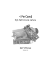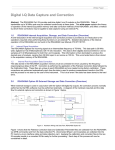
1
PMC-SIO4
User Manual
General Standards Corporation
8302A Whitesburg Drive
Huntsville, AL 35802
Phone: (256) 880-8787
Fax: (256) 880-8788
URL: www.generalstandards.com
E-mail: [email protected]/
PMC-SIO4 Documentation History
1.
2.
October 24, 1997: combined PMC-SIO4 documentation with the latest VME-SIO4 documentation.
November 19, 1997: edited Register map & inserted Zilog data book information into publication section &
deleted non-pertinent information out of Chapter 1.
3. December 1, 1997: edited bit map and bit descriptions, edited section numbering and edited table of
contents.
4. December 2, 1997: edited Chapter 3 hardware configurations.
5. April 17, 1998: Updated bit map.
6. April 20-24, 1998: Drew description of clock jumper configurations
7. April 24, 1998: Inserted PLX / PCI Register maps into Chapter2, moved Local Registers to Chapter 3, updated
section numbering and TOC.
8. May 1, released Manual revision N/R.
9. Updated Register Map (Table 3.0-1, page 53)
10. August, 98: Corrected errors.
11. January, 02: Corrected errors.
12. May 30, 2002: Added Programming Section, corrected errors.
PMC-SIO4 User Manual, Revision: B
General Standards Corporation
8302A Whitesburg Drive Huntsville, AL 35802, Phone: (256) 880-8787
II
PREFACE
Copyright © 1998 General Standards Corp.
Additional copies of this manual or other General Standards Corporation literature may be obtained from:
General Standards Corporation
8302A Whitesburg Drive
Huntsville, Alabama 35802
Telephone: (256) 880-8787
Fax: (256) 880-8788
Company URL: www.generalstandards.com
The information in this document is subject to change without notice.
General Standards Corporation makes no warranty of any kind with regard to this material, including, but not limited
to, the implied warranties of merchantability and fitness for a particular purpose. Although extensive editing and
reviews are performed before release to ECO control, General Standards Corporation assumes no responsibility for
any errors that may exist in this document. No commitment is made to update or keep current the information
contained in this document.
General Standards Corporation does not assume any liability arising out of the application or use of any product or
circuit described herein, nor is any license conveyed under any patent right of any rights of others.
General Standards Corporation assumes no responsibility resulting from omissions or errors in this manual, or from
the use of information contained herein.
General Standards Corporation reserves the right to make any changes, without notice, to this product to improve
reliability, performance, function, or design.
All rights reserved
No parts of this document may be copied or reproduced in any form or by any means without prior written consent of
General Standards Corporation.
This user’s manual provides information on the, register level programming, of the PMC-SIO4 board.
Information required for customized software development.
This manual assumes that the user is familiar with the PCI bus interface specification. In an effort to avoid
redundancy, this manual relies on data books, other manuals, and specifications as indicated in the related
publication section.
RELATED PUBLICATIONS
EIA Standard for the RS-422A Interface (EIA order number EIA-RS-422A)
Draft Standard Physical and Environmental Layers for PCI Mezzanine Cards: PMC
Sponsored by the
Bus Architecture Standards Committee
of the IEEE Computer Society
P1386.1/Draft 2.0
April 4,1995
Sponsor Ballot Draft
For questions or comments regarding this draft, please contact either the chair or draft editor of this proposed
standard:
Wayne Fisher
PMC Chair
2001 Logic Drive
San Jose, CA 95124-3456 USA
Ph: 408-369-6250
Fax: 408-371-3382
Em: [email protected]
Dave Moore
PMC Draft Editor
Digital Equipment Corporation
146 Main Street MLO11-4/U32
Maynard, MA 01754-2571 USA
Ph: 408-493-2257
Fax: 408-493-0652
E-mail: [email protected]
PCI Local Bus Specification Revision 2.1 June 1, 1995. Questions regarding the PCI specification should be forwarded
to:
PCI Special Interest Group
P.O. Box 14070
Portland, OR 97214
(800) 433- 5177 (U.S.)
(503) 797-4207 (International)
(503) 234-6762 (FAX)
Zilog User’s Manual and Product Specifications Databook for the Z16C30 USC requests should be forwarded to:
ZILOG, Inc.
210 East Hacienda Ave.
Campbell, CA 95008-6600
(408) 370-8000
PMC-SIO4 User Manual, Revision: B
General Standards Corporation
8302A Whitesburg Drive Huntsville, AL 35802, Phone: (256) 880-8787
IV
TABLE OF CONTENTS
CHAPTER 1: INTRODUCTION...................................................................................................................................................1
1.0
INTRODUCTION............................................................................................................................................................ 1
1.1
FUNCTIONAL DESCRIPTION..................................................................................................................................... 1
FIGURE 1.1-1 FUNCTIONAL DESCRIPTION............................................................................................................................... 1
1.2
BOARD CONTROL REGISTER.................................................................................................................................... 2
1.3
BOARD STATUS REGISTER....................................................................................................................................... 2
1.4
SYNC WORD SELECTION REGISTERS..................................................................................................................... 2
1.5
DATA RECEPTION ....................................................................................................................................................... 2
1.6
DATA TRANSMISSION .............................................................................................................................................. 2
1.7
ERROR DETECTION...................................................................................................................................................... 2
1.8
INTERRUPTS.................................................................................................................................................................. 2
CHAPTER 2: LOCAL SPACE REGISTERS..............................................................................................................................4
2.0
REGISTER MAP ............................................................................................................................................................. 4
TABLE 2.0-1: PMC-SIO4 REGISTER A DDRESS M AP ............................................................................................................... 4
2.1
BIT MAP FOR LOCAL SPACE REGISTERS.............................................................................................................. 5
2.1.0 FIRMWARE REVISION: (LOC 0X00).............................................................................................................................. 5
2.1.2 CLOCK CONTROL: (LOC 0X0C)..................................................................................................................................... 6
2.1.4 CHANNEL 1 TX A LMOST : (LOC 0X10)........................................................................................................................ 7
2.1.5 CHANNEL 1 RX A LMOST : (LOC 0X14)........................................................................................................................ 7
2.1.6 CHANNEL 1 FIFO: (LOC 0X18) ..................................................................................................................................... 7
2.1.7 CHANNEL 1 CONTROL/STATUS: (LOC 0X1C)............................................................................................................ 7
2.1.8 CHANNEL 2 TX A LMOST : (LOC 0X20)........................................................................................................................ 9
2.1.9 CHANNEL 2 RX A LMOST : (LOC 0X24)....................................................................................................................... 9
2.1.10 CHANNEL 2 FIFO: (LOC 0X28) ..................................................................................................................................... 9
2.1.11 CHANNEL 2 CONTROL/STATUS: (LOC 0X2C)........................................................................................................... 9
2.1.12 CHANNEL 3 TX A LMOST : (LOC 0X30)...................................................................................................................... 10
2.1.13 CHANNEL 3 RX A LMOST : (LOC 0X34)...................................................................................................................... 11
2.1.14 CHANNEL 3 A LMOST : (LOC 0X38) ............................................................................................................................ 11
2.1.15 CHANNEL 3 CONTROL/STATUS: (LOC 0X3C).......................................................................................................... 11
2.1.16 CHANNEL 4 TX A LMOST : (LOC 0X40)...................................................................................................................... 12
2.1.17 CHANNEL 4 RX A LMOST : (LOC 0X44)...................................................................................................................... 12
2.1.18 CHANNEL 4 FIFO: (LOC 0X48) ................................................................................................................................... 12
2.1.19 CHANNEL 4 CONTROL/STATUS: (LOC 0X4C).......................................................................................................... 13
2.1.20 CHANNEL 1 SYNC DETECT : (LOC 0X50).................................................................................................................. 14
2.1.21 CHANNEL 2 SYNC DETECT : (LOC 0X54).................................................................................................................. 14
2.1.22 CHANNEL 3 SYNC DETECT : (LOC 0X58).................................................................................................................. 14
2.1.23 CHANNEL 4 SYNC DETECT : (LOC 0X5C) ................................................................................................................. 14
2.1.24 INTERRUPT CONTROL: (LOC 0X60).......................................................................................................................... 15
2.1.25 INTERRUPT STATUS: (LOC 0X64) ............................................................................................................................. 15
2.3
SERIAL CONTROLLER REGISTERS......................................................................................................................... 16
2.3.1 USC REGISTERS .......................................................................................................................................................... 16
2.3.1.1 CHANNEL 1 USC: (LOC 0X100 TO 0X17E)................................................................................................................ 16
2.3.1.2 CHANNEL 2 USC: (LOC 0X200 TO 0X27E)................................................................................................................ 16
2.3.1.3 CHANNEL 3 USC: (LOC 0X300 0X37E) ...................................................................................................................... 16
2.3.1.4 CHANNEL 4 USC: (LOC 0X400 TO 0X47E)................................................................................................................ 16
2.3.2 CHANNEL COMMAND/A DDRESS REGISTER (CCAR)............................................................................................. 16
2.3.2.1
LOW : (LOC 0XN00)............................................................................................................................................. 16
2.3.2.2
HIGH : (LOC: 0XN01) ........................................................................................................................................... 16
2.3.3 CHANNEL M ODE REGISTER (CMR) .......................................................................................................................... 17
2.3.3.1
LOW : (LOC 0XN02).............................................................................................................................................. 17
2.3.3.2
HIGH : (LOC 0XN03) ............................................................................................................................................. 18
2.3.4 CHANNEL COMMAND/STATUS REGISTER (CCSR)................................................................................................. 18
2.3.4.1
LOW : (LOC 0XN04).............................................................................................................................................. 18
2.3.4.2
HIGH : (LOC 0XN05) ............................................................................................................................................. 19
2.3.5 CHANNEL CONTROL REGISTER (CCR) ..................................................................................................................... 19
2.3.5.1
LOW : (LOC 0XN06).............................................................................................................................................. 19
2.3.5.2
HIGH : (LOC 0XN07) .............................................................................................................................................. 19
2.3.6 PRIMARY RESERVED REGISTER (RESERVED) ......................................................................................................... 20
2.3.6.1
LOW : (LOC 0XN08).............................................................................................................................................. 20
2.3.6.2
HIGH : (LOC 0XN09) ............................................................................................................................................. 20
2.3.7 SECONDARY RESERVED REGISTER (RESERVED).................................................................................................... 20
2.3.7.1
LOW : (LOC 0XNA)............................................................................................................................................... 20
2.3.7.2
HIGH : (LOC 0XNB)............................................................................................................................................... 20
2.3.8 TEST M ODE DATA REGISTER (TMDR).................................................................................................................... 20
2.3.8.1
LOW : (LOC: 0XNC) ............................................................................................................................................. 20
2.3.8.2
HIGH: (LOC 0XN1A)............................................................................................................................................ 20
2.3.9 TEST M ODE CONTROL REGISTER (TMCR) ............................................................................................................. 20
2.3.9.1
LOW : (LOC 0XNE)................................................................................................................................................ 20
2.3.9.2
HIGH : (LOC 0XN0F)............................................................................................................................................. 21
2.3.10 CLOCK M ODE CONTROL REGISTER (CMCR).......................................................................................................... 21
2.3.10.1
LOW : (LOC 0XN10).............................................................................................................................................. 21
2.3.10.2
HIGH : (LOC 0XN11) ............................................................................................................................................. 22
2.3.11 HARDWARE CONFIGURATION REGISTER (HCR)..................................................................................................... 22
2.3.11.1
LOW : (LOC 0XN12).............................................................................................................................................. 22
2.3.11.2
HIGH : (LOC 0XN13) ............................................................................................................................................. 23
2.3.12 INTERRUPT VECTOR REGISTER (IVR)...................................................................................................................... 23
2.3.12.1
LOW : (LOC 0XN14).............................................................................................................................................. 23
2.3.12.2
HIGH : (LOC 0XN2A)............................................................................................................................................ 23
2.3.13 I/O CONTROL REGISTER (IOCR)................................................................................................................................ 23
2.3.13.1
LOW : (LOC 0XN16).............................................................................................................................................. 23
2.3.13.2
HIGH : (LOC 0XN17) ............................................................................................................................................. 24
2.3.14 INTERRUPT CONTROL REGISTER (ICR) ................................................................................................................... 24
2.3.14.1
LOW : (LOC 0XN18).............................................................................................................................................. 24
2.3.14.2
HIGH : (LOC 0XN19) ............................................................................................................................................. 25
2.3.15 DAISY -CHAIN CONTROL REGISTER (DCCR)............................................................................................................ 25
2.3.15.1
LOW : (LOC: 0XN1A)........................................................................................................................................... 25
2.3.15.2
HIGH RW: (LOC 0XN1B)..................................................................................................................................... 25
2.3.16 M ISCELLANEOUS INTERRUPT STATUS REGISTER (MISR).................................................................................. 26
2.3.16.1
LOW : (LOC 0XN1C) ............................................................................................................................................. 26
2.3.16.2
HIGH : (LOC 0XN1D) ............................................................................................................................................ 26
2.3.17 STATUS INTERRUPT CONTROL REGISTER (SICR).................................................................................................. 26
2.3.17.1
LOW : (LOC 0XN1E).............................................................................................................................................. 26
2.3.17.2
HIGH : (LOC 0XN1F)............................................................................................................................................. 26
2.3.18 TX/RX DATA REGISTER (RDR/TDR)........................................................................................................................ 27
2.3.18.1
LOW : (LOC 0XN20).............................................................................................................................................. 27
2.3.18.2
HIGH : (LOC 0XN21) ............................................................................................................................................. 27
2.3.19 RECEIVER M ODE REGISTER (RMR).......................................................................................................................... 27
2.3.19.1
LOW : (LOC 0XN22).............................................................................................................................................. 27
2.3.19.2
HIGH : (LOC 0XN23) ............................................................................................................................................. 28
2.3.20 RECEIVE COMMAND STATUS REGISTER (RCSR).................................................................................................... 28
2.3.20.1
LOW : (LOC 0XN24).............................................................................................................................................. 28
2.3.20.2
HIGH : (LOC 0XN25) ............................................................................................................................................. 28
PMC-SIO4 User Manual, Revision: B
General Standards Corporation
8302A Whitesburg Drive Huntsville, AL 35802, Phone: (256) 880-8787
IV
2.3.21 RECEIVE INTERRUPT CONTROL REGISTER (RICR)................................................................................................ 29
2.3.21.1
LOW : (LOC 0XN26).............................................................................................................................................. 29
2.3.21.2
HIGH : (LOC 0XN27) ............................................................................................................................................. 29
2.3.22 RECEIVE SYNC REGISTER (RSR)................................................................................................................................ 29
2.3.22.1
LOW : (LOC 0XN28).............................................................................................................................................. 29
2.3.22.2
HIGH : (LOC 0XN29) ............................................................................................................................................. 29
2.3.23 RECEIVE COUNT LIMIT REGISTER (RCLR).............................................................................................................. 29
2.3.23.1
LOW : (LOC 0XN2A)............................................................................................................................................. 29
2.3.23.2
HIGH : (LOC 0XN2B)............................................................................................................................................. 29
2.3.24 RECEIVE CHARACTER COUNT REGISTER (RCCR).................................................................................................. 29
2.3.24.1
LOW : (LOC 0XN2C) ............................................................................................................................................. 29
2.3.24.2
HIGH : (LOC 0XN2D) ............................................................................................................................................ 29
2.3.25 TIME CONSTANT 0 REGISTER (TC0R) ...................................................................................................................... 30
2.3.25.1
LOW : (LOC 0XN2E).............................................................................................................................................. 30
2.3.25.2
HIGH : (LOC 0XN2F)............................................................................................................................................. 30
2.3.26 TRANSMIT M ODE REGISTER (TMR)......................................................................................................................... 30
2.3.26.1
LOW : (LOC 0XN32).............................................................................................................................................. 30
2.3.26.2
HIGH : (LOC 0XN33) ............................................................................................................................................. 30
2.3.27 TRANSMIT COMMAND/STATUS REGISTER (TCSR)................................................................................................ 31
2.3.27.1
LOW : (LOC 0XN34).............................................................................................................................................. 31
2.3.27.2
HIGH : (LOC 0XN35) ............................................................................................................................................. 31
2.3.28 TRANSMIT INTERRUPT CONTROL REGISTER (TICR) ............................................................................................ 32
2.3.28.1
LOW : (LOC 0XN36).............................................................................................................................................. 32
2.3.28.2
HIGH : (LOC 0XN37) ............................................................................................................................................. 32
2.3.29 TRANSMIT SYNC REGISTER (TSR) ........................................................................................................................... 32
2.3.29.1
LOW : (LOC 0XN38).............................................................................................................................................. 32
2.3.29.2
HIGH : (LOC 0XN39) ............................................................................................................................................. 32
2.3.30 TRANSMIT COUNT LIMIT REGISTER (TCLR) .......................................................................................................... 32
2.3.30.1
LOW : (LOC 0XN3A)............................................................................................................................................. 32
2.3.30.2
HIGH : (LOC 0XN3B)............................................................................................................................................. 32
2.3.31 TRANSMIT CHARACTER COUNT REGISTER (TCCR) .............................................................................................. 32
2.3.31.1
LOW : (LOC 0XN3C) ............................................................................................................................................. 32
2.3.31.2
HIGH : (LOC 0XN3D) ............................................................................................................................................ 32
2.3.32 TIME CONSTANT 1 REGISTER (TC1R) ..................................................................................................................... 32
2.3.32.1
LOW : (LOC 0XN3E).............................................................................................................................................. 32
2.3.32.2
HIGH : (LOC 0XN3F)............................................................................................................................................. 33
CHAPTER 3: PCI INTERFACE..................................................................................................................................................34
3.0
PCI INTERFACE REGISTERS..................................................................................................................................... 34
3.1
PCI CONFIGURATION REGISTERS ......................................................................................................................... 34
TABLE 3.1-1:
PCI CONFIGURATION REGISTERS............................................................................................................. 34
3.1.1 PCI CONFIGURATION ID REGISTER: (OFFSET 0X00, RESET 0X908010B5)........................................................... 35
3.1.2 PCI 35
3.1.3 PCI STATUS REGISTER: (OFFSET 0X06, RESET 0X0280)......................................................................................... 35
3.1.4 PCI REVISION ID REGISTER : (OFFSET 0X08) ........................................................................................................... 36
3.1.5 PCI CLASS CODE REGISTER: (OFFSET 0X09-0B, RESET =0X068000)...................................................................... 36
3.1.6 PCI CACHE LINE SIZE REGISTER: (OFFSET 0X0C, RESET 0X00)........................................................................... 36
3.1.7 PCI LATENCY TIMER REGISTER : (OFFSET 0X0D, RESET 0X00)........................................................................... 36
3.1.8 PCI HEADER TYPE REGISTER: (OFFSET 0X0E, RESET 0X00)................................................................................. 36
3.1.9 PCI BASE A DDRESS REGISTER FOR M EMORY A CCESS TO LOCAL/RUNTIME/DMA REGISTERS :(OFFSET
0X010, RESET 0X00000000) ........................................................................................................................................... 36
3.1.10 PCI BASE A DDRESS REGISTER FOR I/O A CCESS TO LOCAL/RUNTIME/DMA REGISTERS :.............................. 37
(OFFSET 0X14, RESET 0X00000001) ........................................................................................................................... 37
PMC-SIO4 User Manual, Revision: B
General Standards Corporation
8302A Whitesburg Drive Huntsville, AL 35802, Phone: (256) 880-8787
V
3.1.11 PCI BASE A DDRESS REGISTER FOR M EMORY A CCESS TO LOCAL A DDRESS SPACE 0: .................................... 37
(OFFSET 0X18, RESET 0X00000000) ........................................................................................................................... 37
3.1.12 PCI SUBSYSTEM DEVICE /VENDOR ID REGISTER: (OFFSET 0X2C, RESET 0X908010B5).................................... 37
3.1.13 PCI INTERRUPT LINE REGISTER: (OFFSET 0X3C, RESET 0X00)............................................................................ 37
3.1.14 PCI INTERRUPT PIN REGISTER : (OFFSET 0X3D, RESET 0X01)............................................................................. 38
3.1.15 PCI M IN_GNT REGISTER : (OFFSET 0X3E, RESET 0X00)........................................................................................ 38
3.1.16 PCI M AX_LAT REGIST ER : (OFFSET 0X3F, RESET 0X00)....................................................................................... 38
3.2
LOCAL CONFIGURATION REGISTERS.................................................................................................................. 38
TABLE 3.2-1: LOCAL CONFIGURATION REGISTERS .............................................................................................................. 38
3.2.1 LOCAL A DDRESS SPACE 0 RANGE REGISTER FOR PCI TO LOCAL BUS : ............................................................. 39
(PCI 0X00, RESET 0XFFFFF000)................................................................................................................................. 39
3.2.2 M ODE/A RBITRATION REGISTER : (PCI 0X08)......................................................................................................... 39
3.2.3 BIG/LITTLE ENDIAN DESCRIPTOR REGISTER : (PCI 0X0C)................................................................................... 39
3.2.4 LOCAL A DDRESS SPACE 0/EXPANSION ROM BUS REGION DESCRIPTOR REGISTER........................................ 39
(PCI 0X18, RESET 0X40030143)................................................................................................................................... 39
3.3
RUNTIME REGISTERS............................................................................................................................................... 40
TABLE 3.3-1: RUNTIME REGISTERS........................................................................................................................................ 40
3.3.1 INTERRUPT CONTROL /STATUS : (PCI 0X68, RESET 0X00000000) ...................................................................... 41
3.3.2 SERIAL EEPROM CONTROL, PCI COMMAND CODES, USER I/O CONTROL, INIT CONTROL REGISTER: (PCI 0
X6C, RESET 0X0X001767E).......................................................................................................................................... 41
3.3.3 PCI PERMANENT CONFIGURATION ID REGIST ER : (PCI 0X70, RESET 0X10B59080)......................................... 42
3.3.4 PCI PERMANENT REVISION ID REGISTER: (PCI 0X74) ........................................................................................... 42
3.4
LOCAL DMA REGISTERS.......................................................................................................................................... 42
TABLE 3.4-1: DMA REGISTERS............................................................................................................................................... 42
3.4.1 DMA CHANNEL 0 M ODE REGISTER : (PCI 0X80) ................................................................................................... 42
3.4.2 DMA CHANNEL 0 PCI A DDRESS REGISTER : (PCI 0X84)....................................................................................... 43
3.4.3 DMA CHANNEL 0 LOCAL A DDRESS REGISTER : (PCI 0X88)................................................................................. 43
3.4.4 DMA CHANNEL 0 TRANSFER SIZE (BYTES) REGISTER: (PCI 0X8C).................................................................... 43
3.4.5 DMA CHANNEL 0 DESCRIPTOR POINTER REGISTER : (PCI 0X90)....................................................................... 43
3.4.6 DMA CHANNEL 0 COMMAND/STATUS REGISTER : (PCI 0XA8)........................................................................ 44
3.4.7 DMA A RBITRATION REGISTER : (PCI 0XAC)......................................................................................................... 44
3.4.8 DMA THRESHOLD REGISTER: (PCI 0XB0) ............................................................................................................... 44
3.5
MESSAGING QUEUE REGISTERS............................................................................................................................ 44
CHAPTER 4: PROGRAMMING................................................................................................................................................45
4.0
4.1
4.2
4.3
4.4
4.5
INTRODUCTION.......................................................................................................................................................... 45
RESETS .......................................................................................................................................................................... 45
FIFO ALMOST FLAGS ............................................................................................................................................... 45
PCI DMA ....................................................................................................................................................................... 45
ZILOG Z16C30 DMA ................................................................................................................................................... 46
INTERRUPTS................................................................................................................................................................ 46
CHAPTER 5: HARDWARE CONFIGURATION....................................................................................................................47
5.0
THE ON-BOARD MASTER & TRANSMIT/RECEIVE CLOCKS.......................................................................... 47
5.1
EEPROM JUMPER (J12).............................................................................................................................................. 47
5.2
CABLE INTERFACE CONNECTIONS...................................................................................................................... 47
TABLE 5-2.1: USER CABLE PIN-OUT ....................................................................................................................................... 47
5.3
BOARD LAYOUT ........................................................................................................................................................ 48
FIGURE 5.4-1: BOARD LAYOUT ............................................................................................................................................... 48
5.4
THE ZILOG CLOCK SELECT JUMPERS (J3, J4, J7, & J8)..................................................................................... 48
FIGURE 5.4-2 CLOCK JUMPERS/ROUTING/DATA ROUTING................................................................................................ 50
FIGURE 5.4-4 SIO4 CTS/DCD ROUTING ................................................................................................................................. 50
PMC-SIO4 User Manual, Revision: B
General Standards Corporation
8302A Whitesburg Drive Huntsville, AL 35802, Phone: (256) 880-8787
VI
CHAPTER 6: ORDERING OPTIONS ......................................................................................................................................51
6.0
6.0.1
6.0.2
6.0.3
6.1
ORDERING INFORMATION...................................................................................................................................... 51
CABLE INTERFACE ....................................................................................................................................................... 51
FIFO SIZE ....................................................................................................................................................................... 51
INTERFACE CABLE....................................................................................................................................................... 51
CUSTOM APPLICATIONS ........................................................................................................................................ 51
PMC-SIO4 User Manual, Revision: B
General Standards Corporation
8302A Whitesburg Drive Huntsville, AL 35802, Phone: (256) 880-8787
VII
CHAPTER 1: INTRODUCTION
1.0
INTRODUCTION
The PMC-SI04 interface card is capable of transmitting and receiving serial data, generating interrupts, and
also provides loop-back testing.
This card provides the following specific functionalities:
•
•
•
•
1.1
PMC Bus Interface
Interrupt functionality
FIFOs are provided for data transmit and for data receive to increase the size of the receive buffers.
User interface signal connections are provided via connectors on the front panel.
FUNCTIONAL DESCRIPTION
As shown in the functional block diagram (see Figure 1.1-1), this board includes the following:
•
•
•
•
•
PMC Bus Slave Interface
RS 485/422 Differential Cable Transceivers
2 Universal Serial Controllers (USC), The (Zilog ZI6C30s)
Transmit FIFO Buffers
Receive FIFO Buffers
FIGURE 1.1-1 FUNCTIONAL DESCRIPTION
1.2
BOARD CONTROL REGISTER
The board control register will provide configuration for the PMC/DMA request priorities.
1.3
BOARD STATUS REGISTER
The board status register will provide status of the board (for future expansion).
1.4
SYNC WORD SELECTION REGISTERS
The sync word selection registers are used to provide an interrupt upon the reception of a particular
character on a particular channel. The character is software programmable.
1.5
DATA RECEPTION
Data is received into the Zilog Z16C30. After the data is received, the software may retrieve the data from
the Z16C30 or have the data buffered into the main Rx FIFOs and retrieved by the software at a later time,
depending on how the Z16C30 has been initialized.
1.6
DATA TRANSMISSION
Data is placed into the Zilog Z16C30 or buffered into the main Tx FIFOs, depending on how the Z16C30
has been initialized. The Zilog can transmit and receive in any of several serial protocols:
•
•
•
•
•
•
•
•
•
1.7
Asynchronous
External Sync
Isochronous
Asynchronous with Code Violations
Monosynchronous
Bisynchronous
HDLC
SDLC
Plus many more
ERROR DETECTION
By utilizing the features of the Z16C30, various forms of error detection are built into the board. The
following are some of the methods of error detection available:
•
•
•
•
1.8
Parity error detection
CRC error detection
Rx overrun
Tx underrun
INTERRUPTS
Interrupts will be provided for the following conditions:
•
DMA Complete
PMC-SIO4 User Manual, Revision: B
General Standards Corporation
8302A Whitesburg Drive Huntsville, AL 35802, Phone: (256) 880-8787
2
•
•
•
•
•
•
•
•
•
•
Sync word detected
Tx FIFO almost empty
Rx FIFO almost full
Exited Hunt
IdleRcvd
Break/Abort
RxBound
Abort/ParityError
RxOverrun
Plus many others
PMC-SIO4 User Manual, Revision: B
General Standards Corporation
8302A Whitesburg Drive Huntsville, AL 35802, Phone: (256) 880-8787
3
CHAPTER 2: LOCAL SPACE REGISTERS
2.0
REGISTER MAP
TABLE 2.0-1: PMC-SIO4 REGISTER ADDRESS M AP
Offset
Address
0x00
0x04
0x08
0x0C
0x10
0x14
0x18
0x1C
0x20
0x24
0x28
0x2C
0x30
0x34
0x38
0x3C
0x40
0x44
0x48
0x4C
0x50
0x54
0x58
0x5C
0x60
0x64
0x100
0x200
0x300
0x400
Size
Access*
Register Name
Value
after Programming
D32
D32
RW
RW
0xFFFF0001
0xXXXX0000
D32
D32
D32
D32
D32
D32
D32
D32
D32
D32
D32
D32
D32
D32
D32
D32
D32
D32
D32
D32
D32
D32
D32
D8
D8
D8
D8
RW
RW
RW
RW
RW
RW
RW
RW
RW
RW
RW
RW
RW
RW
RW
RW
RW
RW
RW
RW
RW
RW
RW
see Zilog
Reference
Data Book
Firmware Revision
Board Control
Reserved
Clock Control
Channel 1 Tx Almost
Channel 1 Rx Almost
Channel 1 FIFO
Channel 1 Control/Status
Channel 2 Tx Almost
Channel 2 Rx Almost
Channel 2 FIFO
Channel 2 Control/Status
Channel 3 Tx Almost
Channel 3 Rx Almost
Channel 3 FIFO
Channel 3 Control/Status
Channel 4 Tx Almost
Channel 4 Rx Almost
Channel 4 FIFO
Channel 4 Control/Status
Channel 1 Sync Detected
Channel 2 Sync Detected
Channel 3 Sync Detected
Channel 4 Sync Detected
Interrupt Control
Interrupt Status
Channel 1 USC
Channel 2 USC
Channel 3 USC
Channel 4 USC
0xXXXX0000
0xXXXXXXXX
0xXXXXXXXX
Empty
0xXXXXCCXX
0xXXXXXXXX
0xXXXXXXXX
Empty
0xXXXXCCXX
0xXXXXXXXX
0xXXXXXXXX
Empty
0xXXXXCCXX
0xXXXXXXXX
0xXXXXXXXX
Empty
0xXXXXCCXX
0xXXXXXX00
0xXXXXXX00
0xXXXXXX00
0xXXXXXX00
0x00000000
0x00000000
see Zilog
Reference
Data Book
* RO = read only, WO = write only, RW = read/write capability, BD = Bit Dependent
PMC-SIO4 User Manual, Revision: B
General Standards Corporation
8302A Whitesburg Drive Huntsville, AL 35802, Phone: (256) 880-8787
4
2.1
BIT MAP FOR LOCAL SPACE REGISTERS
When writing to the registers all reserved bits should be set to 0 for future compatibility. In addition, the
value read from a reserved bit will be indeterminate.
2.1.0
FIRMWARE REVISION: (LOC 0 X00)
D0..31 0x00000000
Original Revision
Board Control: (loc 0x04)
D2: 0
210
000
100
010
110
001
101
011
111
Demand Mode DMA Channel 0 Request Encoder
Request DMA on Serial Channel 1 Rx FIFO Almost Full - Hold until Serial Channel 1 Rx FIFO
Almost Empty
Request DMA on Serial Channel 1 Tx FIFO Almost Empty - Hold until Serial Channel 1 Tx FIFO
Almost Full
Request DMA on Serial Channel 2 Rx FIFO Almost Full - Hold until Serial Channel 2 Rx FIFO
Almost Empty
Request DMA on Serial Channel 2 Tx FIFO Almost Empty - Hold until Serial Channel 2 Tx FIFO
Almost Full
Request DMA on Serial Channel 3 Rx FIFO Almost Full - Hold until Serial Channel 3 Rx FIFO
Almost Empty
Request DMA on Serial Channel 3 Tx FIFO Almost Empty - Hold until Serial Channel 3 Rx FIFO
Almost Empty
Request DMA on Serial Channel 4 Rx FIFO Almost Full - Hold until Serial Channel 4 Rx FIFO
Almost Empty
Request DMA on Serial Channel 4 Tx FIFO Almost Empty - Hold until Serial Channel 4 Rx FIFO
Almost Empty
D3
Reserved
D4:6
Demand Mode DMA Channel Request Encoder
654
000
100
010
110
001
101
011
Request DMA on Serial Channel 1 Rx FIFO Almost Full - Hold until Serial Channel 1 Rx FIFO
Almost Empty
Request DMA on Serial Channel 1 Tx FIFO Almost Empty - Hold until Serial Channel 1 Tx FIFO
Almost Full
Request DMA on Serial Channel 2 Rx FIFO Almost Full - Hold until Serial Channel 2 Rx FIFO
Almost Empty
Request DMA on Serial Channel 2 Tx FIFO Almost Empty - Hold until Serial Channel 2 Tx FIFO
Almost Full
Request DMA on Serial Channel 3 Rx FIFO Almost Full - Hold until Serial Channel 3 Rx FIFO
Almost Empty
Request DMA on Serial Channel 3 Tx FIFO Almost Empty - Hold until Serial Channel 3 Rx FIFO
Almost Empty
Request DMA on Serial Channel 4 Rx FIFO Almost Full - Hold until Serial Channel 4 Rx FIFO
Almost Empty
PMC-SIO4 User Manual, Revision: B
General Standards Corporation
8302A Whitesburg Drive Huntsville, AL 35802, Phone: (256) 880-8787
5
111
Request DMA on Serial Channel 4 Tx FIFO Almost Empty - Hold until Serial Channel 4 Rx FIFO
Almost Empty Serial Channel
D31:7
Reserved
2.1.2
CLOCK CONTROL: (LOC 0 X0C)
D0..15 Clock Controls for all 4 channels
D0
D1
D2
D3
D4
D5
D6
D7
D8
D9
D10
Channel 1 Enable Drive Upper Clk
Writing a ‘1’ to this bit will turn on the transmitter for the Channel 1 Tx Clk on the upper
portion of the cable. This will cause this signal on the cable to go from a tri-state
condition to a driven state.
Channel 1 Enable Drive Lower Clk
Writing a ‘1’ to this bit will turn on the transmitter for the Channel 1 Tx Clk on the lower
portion of the cable. This will cause this signal on the cable to go from a tri-state
condition to a driven state.
Channel 1 Enable Receive Upper Clk
Writing a ‘1’ to this bit will turn on the receiver for the Channel 1 Rx clock on the upper
portion of the cable. This will cause this signal on the cable to go from a tri-state condition
to a loaded condition.
Channel 1 Enable Receive Lower Clk
Writing a ‘1’ to this bit will turn on the receiver for the Channel 1 Rx clock on the lower
portion of the cable. This will cause this signal on the cable to go from a tri-state condition
to a loaded condition.
Channel 2 Enable Drive Upper Clk
Writing a ‘1’ to this bit will turn on the transmitter for the Channel 2 Tx Clk on the upper
portion of the cable. This will cause this signal on the cable to go from a tri-state
condition to a driven state.
Channel 2 Enable Drive Lower Clk
Writing a ‘1’ to this bit will turn on the transmitter for the Channel 2 Tx Clk on the lower
portion of the cable. This will cause this signal on the cable to go from a tri-state
condition to a driven state.
Channel 2 Enable Receive Upper Clk
Writing a ‘1’ to this bit will turn on the receiver for the Channel 2 Rx clock on the upper
portion of the cable. This will cause this signal on the cable to go from a tri-state condition
to a loaded condition.
Channel 2 Enable Receive Lower Clk
Writing a ‘1’ to this bit will turn on the receiver for the Channel 2 Rx clock on the lower
portion of the cable. This will cause this signal on the cable to go from a tri-state condition
to a loaded condition.
Channel 3 Enable Drive Upper Clk
Writing a ‘1’ to this bit will turn on the transmitter for the Channel 3 Tx Clk on the upper
portion of the cable. This will cause this signal on the cable to go from a tri-state
condition to a driven state.
Channel 3 Enable Drive Lower Clk
Writing a ‘1’ to this bit will turn on the transmitter for the Channel 3 Tx Clk on the lower
portion of the cable. This will cause this signal on the cable to go from a tri-state
condition to a driven state.
Channel 3 Enable Receive Upper Clk
PMC-SIO4 User Manual, Revision: B
General Standards Corporation
8302A Whitesburg Drive Huntsville, AL 35802, Phone: (256) 880-8787
6
Writing a ‘1’ to this bit will turn on the receiver for the Channel 3 Rx clock on the upper
portion of the cable. This will cause this signal on the cable to go from a tri-state condition
to a loaded condition.
Channel 3 Enable Receive Lower Clk
Writing a ‘1’ to this bit will turn on the receiver for the Channel 3 Rx clock on the lower
portion of the cable. This will cause this signal on the cable to go from a tri-state condition
to a loaded condition.
Channel 4 Enable Drive Upper Clk
Writing a ‘1’ to this bit will turn on the transmitter for the Channel 4 Tx Clk on the upper
portion of the cable. This will cause this signal on the cable to go from a tri-state
condition to a driven state.
Channel 4 Enable Drive Lower Clk
Writing a ‘1’ to this bit will turn on the transmitter for the Channel 4 Tx Clk on the lower
portion of the cable. This will cause this signal on the cable to go from a tri-state
condition to a driven state.
Channel 4 Enable Receive Upper Clk
Writing a ‘1’ to this bit will turn on the receiver for the Channel 4 Rx clock on the upper
portion of the cable. This will cause this signal on the cable to go from a tri-state condition
to a loaded condition.
Channel 4 Enable Receive Lower Clk
Writing a ‘1’ to this bit will turn on the receiver for the Channel 4 Rx clock on the lower
portion of the cable. This will cause this signal on the cable to go from a tri-state condition
to a loaded condition.
D11
D12
D13
D14
D15
2.1.4
CHANNEL 1 TX ALMOST: (LOC 0 X10)
D0..31 Channel 1 Tx Almost Data
The data in this register is used for programming the Almost Flags of the Tx FIFOs for this
channel.
D0..15
Used for the Almost Empty Flag
D16..31
Used for the Almost Full Flag
2.1.5
CHANNEL 1 RX ALMOST: (LOC 0 X14)
D0..31 Channel 1 Rx Almost Data
The data in this register is used for programming the Almost Flags of the Rx FIFOs for this
channel.
D0..15
Used for the Almost Empty Flag
D16..31
Used for the Almost Full Flag
2.1.6
CHANNEL 1 FIFO: (LOC 0 X18)
D0..7
Channel 1 FIFO Data
The FIFOs are setup in a way that the Rx FIFO and the Tx FIFO are located at the same
address. A write to this address will be directed toward the Tx FIFO, and a read from this
address will be directed toward the Rx FIFO.
D8..31 Reserved
2.1.7
D0
CHANNEL 1 CONTROL/STATUS : (LOC 0 X1C)
Reset Channel 1 Tx FIFO (Pulsed)
PMC-SIO4 User Manual, Revision: B
General Standards Corporation
8302A Whitesburg Drive Huntsville, AL 35802, Phone: (256) 880-8787
7
D1
D2
D3
D4
D5
D6
D7
D8
D9
D10
D11
D12
D13
D14
D15
Writing a ‘1’ to this bit will cause the channel 1 Tx FIFOs to be reset. If the channel 1 Tx
Almost register is not a value of 0x00000000 then this will also cause the channel 1 Tx
FIFOs almost flags to be programmed. After setting this bit to a ‘1’, it is the software’s
responsibility to delay approximately 10ms before accessing the local side of the board
again. This bit is a self-timed pulse; therefore, it is not necessary for software to return to
clear this bit, it will clear itself.
Reset Channel 1 Rx FIFO (Pulsed)
Writing a ‘1’ to this bit will cause the channel 1 Rx FIFOs to be reset. If the channel 1 Rx
Almost register is not a value of 0x00000000 then this will also cause the channel 1 Rx
FIFOs almost flags to be programmed. After setting this bit to a ‘1’, it is the software’s
responsibility to delay approximately 10ms before accessing the local side of the board
again. This bit is a self-timed pulse; therefore, it is not necessary for software to return to
clear this bit, it will clear itself.
Enable the Channel 1 Transmitters for the Upper portion of the cable (will drive the
cable)
Writing a ‘1’ to this bit will turn on the transmitters for the Channel 1 upper portion of the
cable. The signals that are turned on are the Channel 1 TxD and Channel 1 CTS on the
upper portion of the cable. This will cause these signals on the cable to go from a tri-state
condition to a driven state.
Enable the Channel 1 Transmitters for the Lower portion of the cable (will drive the
Cable)
Writing a ‘1’ to this bit will turn on the transmitters for the Channel 1 lower portion signals
that are turned on are the Channel 1 TxD and Channel 1 CTS on the lower portion of the
cable. This will cause these signals on the cable to go from a tri-state condition to a driven
state.
Enable the Channel 1 Receivers for the Upper portion of the cable (will load the cable)
Writing a ‘1’ to this bit will turn on the receivers for the Channel 1 upper portion of the
cable. The signals that are turned on are the Channel 1 RxD and Channel 1 DCD on the
upper portion of the cable. This will cause these signals on the cable to go from a tri-state
condition to a loaded condition.
Enable the Channel 1 Receivers for the Lower portion of the cable (will load the cable)
Writing a ‘1’ to this bit will turn on the receivers for the Channel 1 lower portion of the
cable. The signals that are turned on are the Channel 1 RxD and Channel 1 DCD on the
lower portion of the cable. This will cause these signals on the cable to go from a tri-state
condition to a loaded condition.
Reserved
Reset Zilog for Channel 1-2 (Pulsed)
Writing a ‘1’ to this bit will cause the channel 1-2 Zilog Z16C30 USC to be reset. This bit is
a self-timed pulse; therefore, it is not necessary for software to return to clear this bit, it
will clear itself.
Note: After power up and after any reset to this component, the next access to channel 1 or
channel 2 USC must be a write of 0x00 to offset 0x00 of channel 1 USC.
Channel 1 Tx FIFO Empty
(TRUE == 0)
Channel 1 Tx FIFO Almost Empty
(TRUE == 0)
Channel 1 Tx FIFO Almost Full
(TRUE == 0)
Channel 1 Tx FIFO Full
(TRUE == 0)
Channel 1 Rx FIFO Empty
(TRUE == 0)
Channel 1 Rx FIFO Almost Empty
(TRUE == 0)
Channel 1 Rx FIFO Almost Full
(TRUE == 0)
Channel 1 Rx FIFO Full
(TRUE == 0)
The FIFO status flags are active low indicators of the current FIFO status. These flags are continuously
being updated every 33ns. A value of ‘0’ indicates that the current status is true and a value of ‘1’ indicates
PMC-SIO4 User Manual, Revision: B
General Standards Corporation
8302A Whitesburg Drive Huntsville, AL 35802, Phone: (256) 880-8787
8
that it is not true. There are only 5 valid combinations for each nibble (D8..D11 or D12..D15). These
combinations are as follows:
0xC
0xD
0xF
0xB
0x3
2.1.8
1100
1101
1111
1011
0011
Almost Empty and Empty
Almost Empty but not Empty
In between Almost Empty and Almost Full
Almost Full but not full
Almost Full and Full
CHANNEL 2 TX ALMOST: (LOC 0 X20)
D7..0
Channel 2 Tx Almost Data
The data in this register is used for programming the Almost Flags of the Tx FIFOs for this
channel.
D0..15 Used for the Almost Empty Flag
D16..31 Used for the Almost Full Flag
2.1.9
CHANNEL 2 RX ALMOST: (LOC 0 X24)
D0..7
Channel 2 Rx Almost Data
The data in this register is used for programming the Almost Flags of the Tx FIFOs for this
channel.
D0..15 Used for the Almost Empty Flag
D16..31 Used for the Almost Full Flag
2.1.10 CHANNEL 2 FIFO: (LOC 0 X28)
D0..7
Channel 2 FIFO Data
The FIFOs are setup in a way that the Rx FIFO and the Tx FIFO are located at the same
address. A write to this address will be directed toward the Tx FIFO, and a read from this
address will be directed toward the Rx FIFO.
2.1.11 CHANNEL 2 CONTROL/STATUS : (LOC 0 X2C)
D0
D1
D2
Reset Channel 2 Tx FIFO (Pulsed)
Writing a ‘1’ to this bit will cause the channel 2 Tx FIFOs to be reset. If the channel 2 Tx
Almost register is not a value of 0x00000000 then this will also cause the channel 2 Tx
FIFOs almost flags to be programmed. After setting this bit to a ‘1’, it is the software’s
responsibility to delay approximately 10ms before accessing the local side of the board
again. This bit is a self-timed pulse; therefore, it is not necessary for software to return to
clear this bit, it will clear itself.
Reset Channel 2 Rx FIFO (Pulsed)
Writing a ‘1’ to this bit will cause the channel 2 Rx FIFOs to be reset. If the channel 2 Rx
Almost register is not a value of 0x00000000 then this will also cause the channel 2 Rx
FIFOs almost flags to be programmed. After setting this bit to a ‘1’, it is the software’s
responsibility to delay approximately 10ms before accessing the local side of the board
again. This bit is a self-timed pulse; therefore, it is not necessary for software to return to
clear this bit, it will clear itself.
Enable the Channel 2 Transmitters for the Upper portion of the cable (will drive the
cable)
Writing a ‘1’ to this bit will turn on the transmitters for the Channel 2 upper portion of the
cable. The signals that are turned on are the Channel 2 TxD and Channel 2 CTS on the
PMC-SIO4 User Manual, Revision: B
General Standards Corporation
8302A Whitesburg Drive Huntsville, AL 35802, Phone: (256) 880-8787
9
D3
D4
D5
D6
D7
D8
D9
D10
D11
D12
D13
D14
D15
upper portion of the cable. This will cause these signals on the cable to go from a tri-state
condition to a driven state.
Enable the Channel 2 Transmitters for the Lower portion of the cable (will drive the
Cable)
Writing a ‘1’ to this bit will turn on the transmitters for the Channel 2 lower portion of the
cable. The signals that are turned on are the Channel 2 TxD and Channel 2 CTS on the
lower portion of the cable. This will cause these signals on the cable to go from a tri-state
condition to a driven state.
Enable the Channel 2 Receivers for the Upper portion of the cable (will load the cable)
Writing a ‘1’ to this bit will turn on the receivers for the Channel 2 upper portion of the
cable. The signals that are turned on are the Channel 2 RxD and Channel 2 DCD on the
upper portion of the cable. This will cause these signals on the cable to go from a tri-state
condition to a loaded condition.
Enable the Channel 2 Receivers for the Lower portion of the cable (will load the cable)
Writing a ‘1’ to this bit will turn on the receivers for the Channel 2 lower portion of the
cable. The signals that are turned on are the Channel 2 RxD and Channel 2 DCD on the
lower portion of the cable. This will cause these signals on the cable to go from a tri-state
condition to a loaded condition.
Reserved
Reset Zilog for Channel 1-2 (Pulsed)
Writing a ‘1’ to this bit will cause the channel 1-2 Zilog Z16C30 USC to be reset. This bit is
a self-timed pulse; therefore, it is not necessary for software to return to clear this bit, it
will clear itself. Note, that after power up and after any reset to this component, the next
access to channel 1 or channel 2 USC must be a write of 0x00 to offset 0x00 of channel 1
USC.
Channel 2 Tx FIFO Empty
Channel 2 Tx FIFO Almost Empty
Channel 2 Tx FIFO Almost Full
Channel 2 Tx FIFO Full
Channel 2 Rx FIFO Empty
Channel 2 Rx FIFO Almost Empty
Channel 2 Rx FIFO Almost Full
Channel 2 Rx FIFO Full
(TRUE == 0)
(TRUE == 0)
(TRUE == 0)
(TRUE == 0)
(TRUE == 0)
(TRUE == 0)
(TRUE == 0)
(TRUE == 0)
The FIFO status flags are active low indicators of the current FIFO status. These flags are continuously
being updated every 33ns. A value of ‘0’ indicates that the current status is true and a value of ‘1’ indicates
that it is not true. There are only 5 valid combinations for each nibble (D8..D11 or D12..D15). These
combinations are as follows:
0xC
0xD
0xF
0xB
0x3
1100
1101
1111
1011
0011
Almost Empty and Empty
Almost Empty but not Empty
In between Almost Empty and Almost Full
Almost Full but not full
Almost Full and Full
2.1.12 CHANNEL 3 TX ALMOST: (LOC 0 X30)
D0..31 Channel 3 Tx Almost Data
The data in this register is used for programming the Almost Flags of the Tx FIFOs for
this channel.
D0..15 Used for the Almost Empty Flag
PMC-SIO4 User Manual, Revision: B
General Standards Corporation
8302A Whitesburg Drive Huntsville, AL 35802, Phone: (256) 880-8787
10
D16..31 Used for the Almost Full Flag
2.1.13 CHANNEL 3 RX ALMOST: (LOC 0 X34)
D0..31 Channel 3 Rx Almost Data
The data in this register is used for programming the Almost Flags of the Tx FIFOs for this
channel.
D0..15 Used for the Almost Empty Flag
D16..31 Used for the Almost Full Flag
2.1.14 CHANNEL 3 ALMOST: (LOC 0 X38)
D0..7
Channel 3 FIFO Data
The FIFOs are setup in a way that the Rx FIFO and the Tx FIFO are located at the same
address. A write to this address will be directed toward the Tx FIFO, and a read from this
address will be directed toward the Rx FIFO.
2.1.15 CHANNEL 3 CONTROL/STATUS : (LOC 0 X3C)
D0
D1
D2
D3
D4
D5
Reset Channel 3 Tx FIFO (Pulsed)
Writing a ‘1’ to this bit will cause the channel 3 Tx FIFOs to be reset. If the channel 3 Tx
Almost register is not a value of 0x00000000 then this will also cause the channel 3 Tx
FIFOs almost flags to be programmed. After setting this bit to a ‘1’, it is the software’s
responsibility to delay approximately 10ms before accessing the local side of the board
again. This bit is a self-timed pulse; therefore, it is not necessary for software to return to
clear this bit, it will clear itself.
Reset Channel 3 Rx FIFO (Pulsed)
Writing a ‘1’ to this bit will cause the channel 3 Rx FIFOs to be reset. If the channel 3 Rx
Almost register is not a value of 0x00000000 then this will also cause the channel 3 Rx
FIFOs almost flags to be programmed. After setting this bit to a ‘1’, it is the software’s
responsibility to delay approximately 10ms before accessing the local side of the board
again. This bit is a self-timed pulse; therefore, it is not necessary for software to return to
clear this bit, it will clear itself.
Enable the Channel 3 Transmitters for the Upper portion of the cable (will drive the
cable)
Writing a ‘1’ to this bit will turn on the transmitters for the Channel 3 upper portion of the
cable. The signals that are turned on are the Channel 3 TxD and Channel 3 CTS on the
upper portion of the cable. This will cause these signals on the cable to go from a tri-state
condition to a driven state.
Enable the Channel 3 Transmitters for the Lower portion of the cable (will drive the
Cable)
Writing a ‘1’ to this bit will turn on the transmitters for the Channel 3 lower portion of the
cable. The signals that are turned on are the Channel 3 TxD and Channel 3 CTS on the
lower portion of the cable. This will cause these signals on the cable to go from a tri-state
condition to a driven state.
Enable the Channel 3 Receivers for the Upper portion of the cable (will load the cable)
Writing a ‘1’ to this bit will turn on the receivers for the Channel 3 upper portion of the
cable. The signals that are turned on are the Channel 3 RxD and Channel 3 DCD on the
upper portion of the cable. This will cause these signals on the cable to go from a tri-state
condition to a loaded condition.
Enable the Channel 3 Receivers for the Lower portion of the cable (will load the cable)
PMC-SIO4 User Manual, Revision: B
General Standards Corporation
8302A Whitesburg Drive Huntsville, AL 35802, Phone: (256) 880-8787
11
D6
D7
D8
D9
D10
D11
D12
D13
D14
D15
Writing a ‘1’ to this bit will turn on the receivers for the Channel 3 lower portion of the
cable. The signals that are turned on are the Channel 3 RxD and Channel 3 DCD on the
lower portion of the cable. This will cause these signals on the cable to go from a tri-state
condition to a loaded condition.
Reserved
Reset Zilog for Channel 3-4 (Pulsed)
Writing a ‘1’ to this bit will cause the channel 3-4 Zilog Z16C30 USC to be reset. This bit is
a self-timed pulse; therefore, it is not necessary for software to return to clear this bit, it
will clear itself. Note, that after power up and after any reset to this component, the next
access to channel 3 or channel 4 USC must be a write of 0x00 to offset 0x00 of channel 3
USC.
Channel 3 Tx FIFO Empty
(TRUE == 0)
Channel 3 Tx FIFO Almost Empty
(TRUE == 0)
Channel 3 Tx FIFO Almost Full
(TRUE == 0)
Channel 3 Tx FIFO Full
(TRUE == 0)
Channel 3 Rx FIFO Empty
(TRUE == 0)
Channel 3 Rx FIFO Almost Empty
(TRUE == 0)
Channel 3 Rx FIFO Almost Full
(TRUE == 0)
Channel 3 Rx FIFO Full
(TRUE == 0)
The FIFO status flags are active low indicators of the current FIFO status. These flags are continuously
being updated every 33ns. A value of ‘0’ indicates that the current status is true and a value of ‘1’ indicates
that it is not true. There are only 5 valid combinations for each nibble (D8..D11 or D12..D15). These
combinations are as follows:
0xC
0xD
0xF
0xB
0x3
1100
1101
1111
1011
0011
Almost Empty and Empty
Almost Empty but not Empty
In between Almost Empty and Almost Full
Almost Full but not full
Almost Full and Full
2.1.16 CHANNEL 4 TX ALMOST: (LOC 0 X40)
D0..31 Channel 4 Tx Almost Data
The data in this register is used for programming the Almost Flags of the Tx
FIFOs for this channel.
D0..15 is used for the Almost Empty Flag
D16..31 is used for the Almost Full Flag
2.1.17 CHANNEL 4 RX ALMOST: (LOC 0 X44)
D0..31 Channel 4 Rx Almost Data
The data in this register is used for programming the Almost Flags of the Tx FIFOs for
this channel.
D0..15 is used for the Almost Empty Flag
D16..31 is used for the Almost Full Flag
2.1.18 CHANNEL 4 FIFO: (LOC 0 X48)
D0..7
Channel 4 FIFO Data
PMC-SIO4 User Manual, Revision: B
General Standards Corporation
8302A Whitesburg Drive Huntsville, AL 35802, Phone: (256) 880-8787
12
The FIFOs are set in a way that the Rx FIFO and the Tx FIFO are located at the same
address. A write to this address will be directed toward the Tx FIFO, and a read from this
address will be directed toward the Rx FIFO.
2.1.19 CHANNEL 4 CONTROL/STATUS : (LOC 0 X4C)
D0
D1
D2
D3
D4
D5
D6
D7
D8
D9
Reset Channel 4 Tx FIFO (Pulsed)
Writing a ‘1’ to this bit will cause the channel 4 Tx FIFOs to be reset. If the channel 4 Tx
Almost register is not a value of 0x00000000 then this will also cause the channel 4 Tx
FIFOs almost flags to be programmed. After setting this bit to a ‘1’, it is the software’s
responsibility to delay approximately 10ms before accessing the local side of the board
again. This bit is a self-timed pulse; therefore, it is not necessary for software to return to
clear this bit, it will clear itself.
Reset Channel 4 Rx FIFO (Pulsed)
Writing a ‘1’ to this bit will cause the channel 4 Rx FIFOs to be reset. If the channel 4 Rx
Almost register is not a value of 0x00000000 then this will also cause the channel 4 Rx
FIFOs almost flags to be programmed. After setting this bit to a ‘1’, it is the software’s
responsibility to delay approximately 10ms before accessing the local side of the board
again. This bit is a self-timed pulse; therefore, it is not necessary for software to return to
clear this bit, it will clear itself.
Enable the Channel 4 Transmitters for the Upper portion of the cable (will drive the
cable)
Writing a ‘1’ to this bit will turn on the transmitters for the Channel 4 upper portion of the
cable. The signals that are turned on are the Channel 4 TxD and Channel 4 CTS on the
upper portion of the cable. This will cause these signals on the cable to go from a tri-state
condition to a driven state.
Enable the Channel 4 Transmitters for the Lower portion of the cable (will drive the
Cable)
Writing a ‘1’ to this bit will turn on the transmitters for the Channel 4 lower portion of the
cable. The signals that are turned on are the Channel 4 TxD and Channel 4 CTS on the
lower portion of the cable. This will cause these signals on the cable to go from a tri-state
condition to a driven state.
Enable the Channel 4 Receivers for the Upper portion of the cable (will load the cable)
Writing a ‘1’ to this bit will turn on the receivers for the Channel 4 upper portion of the
cable. The signals that are turned on are the Channel 4 RxD and Channel 4 DCD on the
upper portion of the cable. This will cause these signals on the cable to go from a tri-state
condition to a loaded condition.
Enable the Channel 4 Receivers for the Lower portion of the cable (will load the cable)
Writing a ‘1’ to this bit will turn on the receivers for the Channel 4 lower portion of the
cable. The signals that are turned on are the Channel 4 RxD and Channel 4 DCD on the
lower portion of the cable. This will cause these signals on the cable to go from a tri-state
condition to a loaded condition.
Reserved
Reset Zilog for Channel 3-4 (Pulsed)
Writing a ‘1’ to this bit will cause the channel 3-4 Zilog Z16C30 USC to be reset. This bit is
a self-timed pulse; therefore, it is not necessary for software to return to clear this bit, it
will clear itself.
Note: After power up and after any reset to this component, the next access to channel 3
or channel 4 USC must be a write of 0x00 to offset 0x00 of channel 3 USC.
Channel 4 Tx FIFO Empty
Channel 4 Tx FIFO Almost Empty
(TRUE == 0)
(TRUE == 0)
PMC-SIO4 User Manual, Revision: B
General Standards Corporation
8302A Whitesburg Drive Huntsville, AL 35802, Phone: (256) 880-8787
13
D10
D11
D12
D13
D14
D15
Channel 4 Tx FIFO Almost Full
Channel 4 Tx FIFO Full
Channel 4 Rx FIFO Empty
Channel 4 Rx FIFO Almost Empty
Channel 4 Rx FIFO Almost Full
Channel 4 Rx FIFO Full
(TRUE == 0)
(TRUE == 0)
(TRUE == 0)
(TRUE == 0)
(TRUE == 0)
(TRUE == 0)
The FIFO status flags are active low indicators of the current FIFO status. These flags are continuously
being updated every 33ns. A value of ‘0’ indicates that the current status is true and a value of ‘1’ indicates
that it is not true. There are only 5 valid combinations for each nibble (D8..D11 or D12..D15). These
combinations are as follows:
0xC
0xD
0xF
0xB
0x3
1100
1101
1111
1011
0011
Almost Empty and Empty
Almost Empty but not Empty
In between Almost Empty and Almost Full
Almost Full but not full
Almost Full and Full
2.1.20 CHANNEL 1 SYNC DETECT: (LOC 0 X50)
D0..7
Channel 1 Sync Detected Data
The data in this register is used to watch the Rx data as it is being loaded into the
main Rx FIFO. If the data being loaded into the FIFO for this channel matches
this data, then an interrupt request will be generated to the interrupt logic. An
actual interrupt to the host will only occur if this interrupt source is enable in the
interrupt control register.
2.1.21 CHANNEL 2 SYNC DETECT: (LOC 0 X54)
D0..7
Channel 2 Sync Detected Data
The data in this register is used to watch the Rx data as it is being loaded into the
main Rx FIFO. If the data being loaded into the FIFO for this channel
matches this data, then an interrupt request will be generated to the interrupt
logic. An actual interrupt to the host will only occur if this interrupt
source is enable in the interrupt control register.
2.1.22 CHANNEL 3 SYNC DETECT: (LOC 0 X58)
D0..7
Channel 3 Sync Detected Data
The data in this register is used to watch the Rx data as it is being loaded into the
main Rx FIFO. If the data being loaded into the FIFO for this channel matches
this data, then an interrupt request will be generated to the interrupt logic. An
actual interrupt to the host will only occur if this interrupt source is enable in the
interrupt control register.
2.1.23 CHANNEL 4 SYNC DETECT: (LOC 0 X5C)
D0..7
Channel 4 Sync Detected Data
The data in this register is used to watch the Rx data as it is being loaded into the
main Rx FIFO. If the data being loaded into the FIFO for this channel matches
this data, then an interrupt request will be generated to the interrupt logic. An
PMC-SIO4 User Manual, Revision: B
General Standards Corporation
8302A Whitesburg Drive Huntsville, AL 35802, Phone: (256) 880-8787
14
actual interrupt to the host will only occur if this interrupt source is enable in the
interrupt control register.
2.1.24 INTERRUPT CONTROL: (LOC 0 X60)
D0
D1
D2
D3
D4
D5
D6
D7
D8
D9
D10
D11
D12
D13
D14
D15
Enable Channel 1 Interrupt on Sync Detected
Enable Channel 1 Interrupt on Tx FIFO Almost Empty
Enable Channel 1 Interrupt on Rx FIFO Almost Full
Enable Channel 1 Interrupt on USC Request Interrupt
Enable Channel 2 Interrupt on Sync Detected
Enable Channel 2 Interrupt on Tx FIFO Almost Empty
Enable Channel 2 Interrupt on Rx FIFO Almost Full
Enable Channel 2 Interrupt on USC Request
Enable Channel 3 Interrupt on Sync Detected
Enable Channel 3 Interrupt on Tx FIFO Almost Empty
Enable Channel 3 Interrupt on Rx FIFO Almost Full
Enable Channel 3 Interrupt on USC Request Interrupt
Enable Channel 4 Interrupt on Sync Detected
Enable Channel 4 Interrupt on Tx FIFO Almost Empty
Enable Channel 4 Interrupt on Rx FIFO Almost Full
Enable Channel 4 Interrupt on USC Request Interrupt
Note:
A ‘1’ in any of these positions will enable the corresponding interrupt source to perform a
PMC interrupt. A ‘0’ in any of these positions will disable the corresponding interrupt
source from performing a PMC interrupt.
2.1.25 INTERRUPT STATUS : (LOC 0 X64)
D0
D1
D2
D3
D4
D5
D6
D7
D8
D9
D10
D11
D12
D13
D14
D15
Status on Channel 1 Interrupt for Sync Detected
Status on Channel 1 Interrupt for Tx FIFO Almost Empty
Status on Channel 1 Interrupt for Rx FIFO Almost Full
Status on Channel 1 Interrupt for USC Request Interrupt
Status on Channel 2 Interrupt for Sync Detected
Status on Channel 2 Interrupt for Tx FIFO Almost Empty
Status on Channel 2 Interrupt for Rx FIFO Almost Full
Status on Channel 2 Interrupt for USC Request
Status on Channel 3 Interrupt for Sync Detected
Status on Channel 3 Interrupt for Tx FIFO Almost Empty
Status on Channel 3 Interrupt for Rx FIFO Almost Full
Status on Channel 3 Interrupt for USC Request Interrupt
Status on Channel 4 Interrupt for Sync Detected
Status on Channel 4 Interrupt for Tx FIFO Almost Empty
Status on Channel 4 Interrupt for Rx FIFO Almost Full
Status on Channel 4 Interrupt for USC Request Interrupt
Note:
A ‘1’, in any of these positions, will indicate that the corresponding source has either
performed a PMC interrupt or that the source for the interrupt is currently active; thus, could
perform a PMC interrupt if enabled in the interrupt control register. Whether or not the
interrupt was performed depends on the interrupt control register.
If the corresponding bit in the interrupt control register is a ‘0’, then the source has not performed a PMC
interrupt and is only indicating the current status of that source. If the corresponding bit in the interrupt
PMC-SIO4 User Manual, Revision: B
General Standards Corporation
8302A Whitesburg Drive Huntsville, AL 35802, Phone: (256) 880-8787
15
control register is a ‘1’, then the source has performed a PMC interrupt and has latched itself. Writing a ‘1’
to the respective bit in the interrupt status register clears the interrupt status bit. A second interrupt will not
occur until after that status bit has been cleared. The interrupts are not queued; hence, each potential
interrupt should be observed when identifying the source and clearing the status register. Failure to do so
could prevent any other interrupts from occurring.
2.3
SERIAL CONTROLLER REGISTERS
IMPORTANT: Write to Loc 0x100 and Loc 0x300 after every reset to confirm the USC address system.
Contact your local Zilog Representative for Data books and User manuals in reference to the Z16C30, USC
Universal Serial Controller, for a more detailed description of the following registers. It is the advice of the
design engineer of this product that both books should be obtained by any persons desiring to design
using this product. See Related Publications section of this document for address of Zilog.
Note: In the following register addresses ‘n’ stands for Channel Number.
2.3.1
USC REGISTERS
2.3.1.1
CHANNEL 1 USC: (LOC 0 X100 TO 0 X17E)
D0..7
Channel 1 USC Data
2.3.1.2
CHANNEL 2 USC: (LOC 0 X200 TO 0 X27E)
D0..7
Channel 2 USC Data
2.3.1.3
(Zilog Data Bus, See Serial Controller Registers)
CHANNEL 3 USC: (LOC 0 X300 0 X37E)
D0..7
Channel 3 USC Data
2.3.1.4
(Zilog Data Bus, See Serial Controller Registers)
CHANNEL 4 USC: (LOC 0 X400 TO 0 X47E)
D0..7
2.3.2
(Zilog Data Bus, See Serial Controller Registers)
Channel 4 USC Data
(Zilog Data Bus, See Serial Controller Registers)
CHANNEL COMMAND/ADDRESS REGISTER (CCAR)
(Same format for Channels 0..3 USC Control Registers)
2.3.2.1
LOW: (LOC 0 XN00)
D0
D1..D5
D6
D7
WO
WO
WO
WO
Upper/Lower Byte Select
Address 4..0
Byte/Word Access
DMA Continue
The contents of this register should always be set to 0x00 for this product.
2.3.2.2
HIGH: (LOC: 0 XN01)
PMC-SIO4 User Manual, Revision: B
General Standards Corporation
8302A Whitesburg Drive Huntsville, AL 35802, Phone: (256) 880-8787
16
D0..D1 WO
D9 D8
0 0
0 1
1 0
1 1
D2
D3..7
Mode Control (encoded as follows):
Normal Operation
Auto Echo
External Local Loop-back
Internal Local Loop-back
Channel Reset
WO
Channel Command (encoded as follows, D11 as the LSB):
00000 Null Command
00001 Reserved
00010 Reset Highest IUS
00011 Trigger Channel Load DMA
00101 Trigger Rx DMA
00110 Trigger Tx DMA
00111 Trigger Rx & Tx DMA
00100 Reserved
00100 Rx FIFO Purge
00101Tx FIFO Purge
01011 Rx & Tx FIFO Purge
01100 Reserved
01101 Load Rx Character Count
01110 Load Tx Character Count
01111 Reserved
10000 Load TC0
10001 Load TC1
10010 Load TC0 & TC1
10011 Select Serial Data LSB First*
10100 Select Serial Data MSB First
10101 Select Straight Memory Data*
10110 Select Swapped Memory Data
10111 Reserved
11000 Rx Purge
11001 Reserved
11010 Reserved
11011 Reserved
11100 Reserved
11101 Reserved
11110 Reserved
11111 Reserved
*Selected upon reset
2.3.3
CHANNEL M ODE REGISTER (CMR)
2.3.3.1
LOW: (LOC 0 XN02)
D0..D3 WO
Receiver Mode (encoded as follows):
PMC-SIO4 User Manual, Revision: B
General Standards Corporation
8302A Whitesburg Drive Huntsville, AL 35802, Phone: (256) 880-8787
17
0000
0001
0010
0011
0100
0101
0110
0111
1000
1001
1010
1011
1100
1101
1110
1111
Asynchronous
External Synchronous
Isochronous
Asynchronous with CV
Monosync
Bisync
HDLC
Transparent Bisync
NBIP
802.3
Reserved
Reserved
Reserved
Reserved
Reserved
Reserved
D4..D7 Rx Submode 3..0
2.3.3.2
D0..3
HIGH: (LOC 0 XN03)
Transmitter Mode (encoded as follows):
0000
0001
0010
0011
0100
0101
0110
0111
1000
1001
1010
1011
1100
1101
1110
1111
D4..7
2.3.4
Asynchronous
Reserved
Isochronous
Asynchronous with CV
Monosync
Bisync
HDLC
Transparent Bisync
NBIP
802.3
Reserved
Reserved
Slaved Monosync
Reserved
HDLC Loop
Reserved
Tx Submode 3..0
CHANNEL COMMAND/STATUS REGISTER (CCSR)
2.3.4.1
D0
D1
D2..4
LOW: (LOC 0 XN04)
RO
RxACK
RO
TxACK
HDLC Tx Last Character Length (encoded as follows):
000
001
8 bits
1 bit
PMC-SIO4 User Manual, Revision: B
General Standards Corporation
8302A Whitesburg Drive Huntsville, AL 35802, Phone: (256) 880-8787
18
D5
D6
D7
2.3.4.2
D0..1
D2
D3
D4
D5
D6
D7
2.3.5
010
2 bits
011
3 bits
100
4 bits
101
5 bits
110
6 bits
111
7 bits
Reserved
RO
Loop Sending
RO
On Loop
HIGH: (LOC 0 XN05)
DPLL Adjust/Sync Edge (encoded as follows):
00
01
10
11
Both Edges
Rising Edge Only
Falling Edge Only
Adjust/Sync Inhibit
RW
RW
RW
WO
RO
RO
Clocks Missed Latched/Unlatch
Clocks Missed Latched/Unlatch
DPLL in Sync/Quick Sync
RCC FIFO Clear
RCC FIFO Valid
RCC FIFO Overflow
CHANNEL CONTROL REGISTER (CCR)
2.3.5.1
LOW: (LOC 0 XN06)
D0..4
D5
D6..7
00
01
10
11
2.3.5.2
D0..1
D2..3
D4
D6..7
Reserved
Wait for Rx DMA Trigger
Rx Status Block Transfer (encoded as follows, D6 being the LSB):
No Status Block
One word Status Block
Two word Status Block
Reserved
HIGH: (LOC 0 XN07)
Tx Preamble Pattern (encoded as follows):
00
All Zeros
01
All Ones
10
Alternating 1 & 0
11
Alternating 0 & 1
Tx Preamble Length (encoded as follows):
00
8 bits
01
16 bits
10
32 bits
11
64 bits
Tx Flag Preamble
Tx Status Block Transfer (encoded as follows):
PMC-SIO4 User Manual, Revision: B
General Standards Corporation
8302A Whitesburg Drive Huntsville, AL 35802, Phone: (256) 880-8787
19
00
01
10
11
2.3.6
PRIMARY RESERVED REGISTER (RESERVED)
2.3.6.1
LOW: (LOC 0 XN08)
D0..D7 RW
2.3.6.2
LOW: (LOC 0 XNA)
D0..D7 RW
2.3.7.2
Reserved
HIGH: (LOC 0 XNB)
D0..D7 RW
Reserved
TEST M ODE DATA REGISTER (TMDR)
2.3.8.1
LOW: (LOC: 0 XNC)
D0..D7 RW
2.3.8.2
Test Data 7..0
HIGH: (LOC 0 XN1A)
D0..D7 RW
2.3.9
Reserved
SECONDARY RESERVED REGISTER (RESERVED)
2.3.7.1
2.3.8
Reserved
HIGH: (LOC 0 XN09)
D0..D7 RW
2.3.7
No Status Block
One word Status Block
Two word Status Block
Reserved
Test Data 7..0
TEST M ODE CONTROL REGISTER (TMCR)
2.3.9.1
D0..4
LOW: (LOC 0 XNE)
Test Regis ter Address (encoded as follows):
00000
00001
00010
00011
00100
00101
00110
00111
01000
01001
01010
Null Address
High Byte of Shifters
CRC Byte 0
CRC Byte 1
Rx FIFO (Write)
Clock Multiplexer Outputs
CTR0 and CTR1 Counters
Clock Multiplexer Inputs
DPLL State
Low Byte of Shifters
CRC Byte 2
PMC-SIO4 User Manual, Revision: B
General Standards Corporation
8302A Whitesburg Drive Huntsville, AL 35802, Phone: (256) 880-8787
20
D5..7
2.3.9.2
D0..7
01011
01100
01101
01110
01111
10000
10001
10010
10011
10100
10101
10110
10111
11000
11001
11010
11011
11100
11101
11110
11111
CRC Byte 3
Tx FIFO (Read)
Reserved
I/O and Device Status Latches
Internal Daisy Chain
Reserved
Reserved
Reserved
Reserved
Reserved
Reserved
Reserved
Reserved
4044H
4044H
4044H
4044H
4044H
4044H
4044H
4044H
RW
Reserved
HIGH: (LOC 0 XN0F)
RW
Reserved
2.3.10 CLOCK M ODE CONTROL REGISTER (CMCR)
2.3.10.1
D0..2
D3..5
LOW: (LOC 0 XN10)
RW
Receive Clock Source (encoded as follows):
000
001
010
011
100
101
110
111
Disabled
/RxC Pin
/TxC Pin
DPLL Output
BRG0 Output
BRG1 Output
CTR0 Output
CTR1 Output
RW
Transmit Clock Source (encoded as follows):
000
001
010
011
100
101
110
Disabled
/RxC Pin
/TxC Pin
DPLL Output
BRG0 Output
BRG1 Output
CTR0 Output
PMC-SIO4 User Manual, Revision: B
General Standards Corporation
8302A Whitesburg Drive Huntsville, AL 35802, Phone: (256) 880-8787
21
D6..7
2.3.10.2
111
CTR1 Output
RW
DPLL Clock Source (encoded as follows):
00
01
10
11
BRG0 Output
BRG1 Output
/RxC Pin
/TxC Pin
HIGH: (LOC 0 XN11)
D0..1
BRG0 Clock Source (encoded as follows):
00
CTR0 Output
01
CTR1 Output
10
/RxC Pin
11
/TxC Pin
D2..3
BRG1 Clock Source (encoded as follows):
00
CTR0 Output
01
CTR1 Output
10
/RxC Pin
11
/TxC Pin
D4..5
CRT0 Clock Source (encoded as follows):
00
BRG0 Output
01
BRG1 Output
10
/RxC Pin
11
/TxC Pin
D6..7
CTR1 Clock Source (encoded as follows):
00
Disabled
01
Disabled
10
/RxC Pin
11
/TxC Pin
2.3.11 HARDWARE CONFIGURATION REGISTER (HCR)
2.3.11.1
D1
D0
D2..3
D5
D4
D6..7
LOW: (LOC 0 XN12)
RW
BRG0 Enable
RW
BRG0 Single Cycle/Continuous
Rx ACK Pin Control (encoded as follows):
00
3 - State Output
01
Rx Acknowledge Input
10
Output 0
11
Output 1
RW
BRG1 Enable
RW
BRG1 Single Cycle/Continuous
Tx ACK Pin Control (encoded as follows):
00
3 - State Output
01
Tx Acknowledge Input
10
Output 0
PMC-SIO4 User Manual, Revision: B
General Standards Corporation
8302A Whitesburg Drive Huntsville, AL 35802, Phone: (256) 880-8787
22
11
2.3.11.2
Output 1
HIGH: (LOC 0 XN13)
D0..D1 DPLL Mode (encoded as follows):
00
Disabled
01
NRZ/NRZI
10
Biphase-Mark/Space
11
Biphase-Level
D2..D3 DPLL Clock Rate (encoded as follows):
00
32x Clock Mode
01
16x Clock Mode
10
8x Clock Mode
11
Reserved
D4
RW
Accept Code Violations
D5
RW
CTR1 Rate Match DPLL/CTR0
D6..7
CTR0 Clock Rate (encoded as follows):
00
32x Clock Mode
01
16x Clock Mode
10
8x Clock Mode
11
4x Clock Mode
2.3.12 INTERRUPT VECTOR REGISTER (IVR)
2.3.12.1
D1..3
2.3.12.2
D4..7
LOW: (LOC 0 XN14)
RW
IV 7..0
HIGH: (LOC 0 XN2A)
RO
000
001
010
011
100
101
110
111
D12..15 RO
Modified Vector (encoded as follows):
None
Device Status
I/O Status
Transmit Data
Transmit Status
Receive Data
Receive Status
Not Used
IV 7..4
2.3.13 I/O CONTROL REGISTER (IOCR)
2.3.13.1
D0..2
LOW: (LOC 0 XN16)
RxC Pin Control (encoded as follows):
000
Input Pin
001
Rx Clock Output
010
Rx Byte Clock Output
011
SYNC Output
100
BRG0 Output
PMC-SIO4 User Manual, Revision: B
General Standards Corporation
8302A Whitesburg Drive Huntsville, AL 35802, Phone: (256) 880-8787
23
101
BRG1 Output
110
CTR0 Output
111
DPLL Rx Output
D3..D5 TxC Pin Control (encoded as follows):
000
Input Pin
001
Tx Clock Output
010
Tx Byte Clock Output
011
Tx Complete Output
100
BRG0 Output
101
BRG1 Output
110
CTR1 Output
111
DPLL Tx Output
D6..7
TxD Pin Control (encoded as follows):
00
Tx Data Output
01
3-State Output
10
Output 0
11
Output 1
2.3.13.2
HIGH: (LOC 0 XN17)
D0..D1 RxREQ Pin Control (encoded as follows):
00
Input pin
01
Rx DMA Request Output
10
Output 0
11
Output 1
D2..D3 TxREQ Pin Control (encoded as follows):
00
Input pin
01
Tx DMA Request Output
10
Output 0
11
Output 1
D4..5
DCD Pin Control (encoded as follows):
00
/DCD Input
01
/DCD//SYNC Input
10
Output 0
11
Output 1
D6..7
CTS Pin Control (encoded as follows):
00
/CTS Input
01
/CTS Input
10
Output 0
11
Output 1
2.3.14
INTERRUPT CONTROL REGISTER (ICR)
2.3.14.1
D0
D1
D2
D3
D4
D5
D6..7
LOW: (LOC 0 XN18)
RW
Device Status IE
RW
I/O Status IE
RW
Transmit Data IE
RW
Transmit Status IE
RW
Receive Data IE
RW
Receive Status IE
IE Command (encoded as follows):
PMC-SIO4 User Manual, Revision: B
General Standards Corporation
8302A Whitesburg Drive Huntsville, AL 35802, Phone: (256) 880-8787
24
00
01
10
11
2.3.14.2
D0
D1..3
D4
D5
D6
D7
Null Command
Null Command
Reset IE
Set IE
HIGH: (LOC 0 XN19)
RW
000
001
010
011
100
101
110
111
RW
RW
RW
RW
Reserved
VIS Level (encoded as follows):
All
All
I/O Status and Above
Transmit Data and Above
Transmit Status and Above
Receive Data and Above
Receive Status Only
None
MIE
DLC
NV
VIS
2.3.15 DAISY-CHAIN CONTROL REGISTER (DCCR)
2.3.15.1
D0
D1
D2
D3
D4
D5
D6..7
2.3.15.2
D0
D1
D2
D3
D4
D5
D6..7
LOW: (LOC: 0 XN1A)
RW
Device Status INTERRUPT PENDING
RW
I/O Status INTERRUPT PENDING
RW
Transmit Data INTERRUPT PENDING
RW
Transmit Status INTERRUPT PENDING
RW
Receive Data INTERRUPT PENDING
RW
Receive Status INTERRUPT PENDING
INTERRUPT PENDING Command (encoded as follows):
00
Null Command
01
Reset INTERRUPT PENDING and IUS
10
Reset INTERRUPT PENDING
11
Set INTERRUPT PENDING
HIGH RW: (LOC 0 XN1B)
RW
Device Status IUS
RW
I/O Status IUS
RW
Transmit Data IUS
RW
Transmit Status IUS
RW
Receive Data IUS
RW
Receive Status IUS
IUS Command (encoded as follows):
Null Command
Null Command
10
Reset IUS
11
Set IUS
PMC-SIO4 User Manual, Revision: B
General Standards Corporation
8302A Whitesburg Drive Huntsville, AL 35802, Phone: (256) 880-8787
25
2.3.16 M ISCELLANEOUS INTERRUPT STATUS REGISTER (MISR)
2.3.16.1
D0
D1
D2
D3
D4
D5
D6
D7
2.3.16.2
D0
D1
D2
D3
D4
D5
D6
D7
2.3.17
LOW: (LOC 0 XN1C)
RW
RW
RW
RW
RO
RW
RO
RW
BRG0 ZC Latched/Unlatch
BRG1 ZC Latched/Unlatch
DPLL SYNC Latched/Unlatch
RCC Overflow Latched/Unlatch
/CTS
/CTS Latched/Unlatch
/DCD
/DCD Latched/Unlatch
HIGH: (LOC 0 XN1D)
RO
RW
RO
RW
RO
RW
RO
RW
TxREQ
/TxREQ Latched/Unlatch
/RxREQ
/RxREQ Latched/Unlatch
/TxC
/TxC Latched/Unlatch
/RxC
/RxC Latched/Unlatch
STATUS INTERRUPT CONTROL
2.3.17.1
D0
D1
D2
D3
D4..5
D6..7
2.3.17.2
REGISTER (SICR)
LOW: (LOC 0 XN1E)
RW
RW
RW
RW
RW
00
01
10
11
RW
00
01
10
11
BRG0 ZC INTERRUPT ENABLE
BRG1 ZC INTERRUPT ENABLE
DPLL SYNC INTERRUPT ENABLE
RCC Overflow INTERRUPT ENABLE
/CTS Interrupts (encoded as follows, D4 being the LSB):
Disabled
Rising Edge Only
Falling Edge Only
Both Edges
/DCD Interrupts (encoded as follows, D6 being the LSB):
Disabled
Rising Edge Only
Falling Edge Only
Both Edges
HIGH: (LOC 0 XN1F)
D0..1
RW
00
01
10
11
/TxREQ Interrupts (encoded as follows):
Disabled
Rising Edge Only
Falling Edge Only
Both Edges
D3..2
RW
/RxREQ Interrupts (encoded as follows):
PMC-SIO4 User Manual, Revision: B
General Standards Corporation
8302A Whitesburg Drive Huntsville, AL 35802, Phone: (256) 880-8787
26
D4..5
D6..7
00
01
10
11
Disabled
Rising Edge Only
Falling Edge Only
Both Edges
RW
00
01
10
11
RW
00
01
10
11
TxC Interrupts (encoded as follows, D12 being the LSB):
Disabled
Rising Edge Only
Falling Edge Only
Both Edges
RxC Interrupts (encoded as follows, D14 being the LSB):
Disabled
Rising Edge Only
Falling Edge Only
Both Edges
2.3.18 TX/RX DATA REGISTER (RDR/TDR)
2.3.18.1
D0..7
2.3.18.2
D0..7
LOW: (LOC 0 XN20)
RW
Tx/Rx D7..0
HIGH: (LOC 0 XN21)
RW
Tx/Rx D7..0
2.3.19 RECEIVER M ODE REGISTER (RMR)
2.3.19.1
D0..1
D2..4
D5
D6..7
LOW: (LOC 0 XN22)
Rx Enable (encoded as follows):
00
Disable Immediately
01
Disable After Reception
10
Enable Without Auto-Enables
11
Enable With Auto-Enables
Rx Character Length (encoded as follows):
000
8 Bits
001
1 Bits
010
2 Bits
011
3 Bits
100
4 Bits
101
5 Bits
110
6 Bits
111
7 Bits
RW
00
01
10
11
Rx Parity Enable
Rx Parity Sense (encoded as follows):
Even
Odd
Space
Mark
PMC-SIO4 User Manual, Revision: B
General Standards Corporation
8302A Whitesburg Drive Huntsville, AL 35802, Phone: (256) 880-8787
27
2.3.19.2
D0
D1
D2
D3..4
HIGH: (LOC 0 XN23)
RW
RW
RW
00
01
10
11
D5..7
000
001
010
011
100
101
110
111
Queue Abort
Rx CRC Enable
Rx CRC Preset Value
Rx CRC Polynomial (encoded as follows):
CRC-CCITT
CRC-16
CRC-32
Reserved
Rx Data Decoding (encoded as follows):
NRZ
NRZB
NRZI-Mark
NRZI-Space
Biphase-Mark
Biphase-Space
Biphase-Level
Diff. Biphase-Level
2.3.20 RECEIVE COMMAND STATUS REGISTER (RCSR)
2.3.20.1
D0
D1
D2
D3
D4
D5
D6
D7
2.3.20.2
D0
D1
D2
D3
D4..7
LOW: (LOC 0 XN24)
RO
RW
RW
RO
RW
RW
RW
RW
Rx Character Available
Rx Overrun
Parity Error/Frame Abort
CRC/Framing Error
Rx CV/EOT/EOF
Rx Break Abort
Rx Idle
Exited Hunt
HIGH: (LOC 0 XN25)
RO
RO
RO
RO
WO
0000
0001
0010
0011
0100
0101
0110
0111
1000
1001
1010
1011
Short Frame/CV Polarity
Residue Code 0
Residue code 1
Residue Code 2
Receive Command (encoded as follows, D12 being the LSB):
Null command
Reserved
Preset CRC
Enter Hunt Mode
Reserved
Select FIFO Status
Select FIFO Interrupt Level
Select FIFO Request Level
Reserved
Reserved
Reserved
Reserved
PMC-SIO4 User Manual, Revision: B
General Standards Corporation
8302A Whitesburg Drive Huntsville, AL 35802, Phone: (256) 880-8787
28
D6
D7
1100
Reserved
Reserved
1110
Reserved
1111
Reserved
RO
First Byte in Error
RO
Second Byte in Error
2.3.21 RECEIVE INTERRUPT CONTROL REGISTER (RICR)
2.3.21.1
D0
D1
D2
D3
D4
D5
D6
D7
2.3.21.2
D0..7
LOW: (LOC 0 XN26)
RW
RW
RW
RW
RW
RW
RW
RW
TC0R Read Count/TC
Rx Overrun INTERRUPT ARMED
Parity Error/Frame Abort INTERRUPT ARMED
Status on Words
Rx CV/EOT/EOF INTERRUPT ARMED
Rx Break/Abort INTERRUPT ARMED
Rx Idle INTERRUPT ARMED
Exited Hunt INTERRUPT ARMED
HIGH: (LOC 0 XN27)
RW
Rx FIFO Control and Status (Fill/Interrupt/DMA Level)
2.3.22 RECEIVE SYNC REGISTER (RSR)
2.3.22.1
D0..7
2.3.22.2
D0..7
LOW: (LOC 0 XN28)
RW
RSYN 0..7
HIGH: (LOC 0 XN29)
RW
RSYN 15..8
2.3.23 RECEIVE COUNT LIMIT REGISTER (RCLR)
2.3.23.1
D0..7
2.3.23.2
D0..7
LOW: (LOC 0 XN2A)
RW
RCL 7..0
HIGH: (LOC 0 XN2B)
RW
RCL 15..8
2.3.24 RECEIVE CHARACTER COUNT REGISTER (RCCR)
2.3.24.1
D0..7
2.3.24.2
LOW: (LOC 0 XN2C)
RO
RCC 7..0
HIGH: (LOC 0 XN2D)
PMC-SIO4 User Manual, Revision: B
General Standards Corporation
8302A Whitesburg Drive Huntsville, AL 35802, Phone: (256) 880-8787
29
D0..7
RO
RCC 15..8
2.3.25 TIME CONSTANT 0 REGISTER (TC0R)
2.3.25.1
D0..7
2.3.25.2
D0..7
LOW: (LOC 0 XN2E)
RW
TC0 7..0
HIGH: (LOC 0 XN2F)
RW
TC0 15..8
2.3.26 TRANSMIT M ODE REGISTER (TMR)
2.3.26.1
LOW: (LOC 0 XN32)
D0..1
Tx Enable (encoded as follows, D0 being the LSB):
00
Disable Immediately
01
Disable After Transmission
10
Enable Without Auto-Enables
11
Enable With Auto-Enables
D2..4
Tx Character Length (encoded as follows):
000
8 Bits
001
1 Bit
010
2 Bits
011
3 Bits
100
4 Bits
101
5 Bits
110
6 Bits
111
7 Bits
RW
Tx Parity Enable
Tx Parity Sense (encoded as follows):
00
Even
01
Odd
10
Space
11
Mark
D5
D6..7
2.3.26.2
HIGH: (LOC 0 XN33)
D0
D1
D2
RW
RW
RW
D3..4
Polynomial Tx CRC (encoded as follows):
00
CRC-CCITT
01
CRC-16
10
CRC-32
11
Reserved
Tx Data Encoding (encoded as follows):
000
NRZ
D5..7
Tx CRC EOF/EOM
Tx CRC Enable
Tx CRC on Preset Value
PMC-SIO4 User Manual, Revision: B
General Standards Corporation
8302A Whitesburg Drive Huntsville, AL 35802, Phone: (256) 880-8787
30
001
010
011
100
101
110
111
NRZB
NRZI-Mark
NRZI-Space
Biphase-Mark
Biphase-Space
Biphase-Level
Diff. Biphase-Level
2.3.27 TRANSMIT COMMAND/STATUS REGISTER (TCSR)
2.3.27.1
D0
D1
D2
D3
D4
D5
D6
D7
2.3.27.2
D0..2
D3
D4..7
LOW: (LOC 0 XN34)
RO
RW
RO
RW
RW
RW
RW
RW
Tx Buffer Empty
Tx Underrun
All Sent
Tx CRC Sent
Tx EOF/EOT Sent
Tx Abort Sent
Tx Idle Sent
Tx Preamble Sent
HIGH: (LOC 0 XN35)
Tx Idle Line Condition
000
SYNC/Flag/Normal
001
Alternating 1 & 0
010
All Zeros
011
All Ones
100
Reserved
101
Alternating Mark & Space
110
Space
111
Mark
RW
TxWait on Underrun
WO
Transmit Command
0000
Null Command
0001
Reserved
0010
Preset CRC
0011
Reserved
0100
Reserved
0101
Select FIFO Status
1110
Select FIFO Interrupt Level
0111
Select FIFO Request Level
1000
Send Frame/Message
1001
Send Abort
1010
Reserved
1011
Reserved
1100
Reset DLE Inhibit
1101
Set DLE Inhibit
1110
Reset EOF/EOM
1111
Set EOF/EOM
PMC-SIO4 User Manual, Revision: B
General Standards Corporation
8302A Whitesburg Drive Huntsville, AL 35802, Phone: (256) 880-8787
31
2.3.28 TRANSMIT INTERRUPT CONTROL REGISTER (TICR)
2.3.28.1
D0
D1
D2
D3
D4
D5
D6
D7
2.3.28.2
D0..7
LOW: (LOC 0 XN36)
RW
RW
RW
RW
RW
RW
RW
RW
TC1R Read Count/TC
Tx Overrun INTERRUPT ARMED
Wait for Send Command
Tx CRC Sent INTERRUPT ARMED
Tx EOF/EOT Sent INTERRUPT ARMED
Tx Abort Sent INTERRUPT ARMED
Tx Idle Sent INTERRUPT ARMED
Tx Preamble Sent INTERRUPT ARMED
HIGH: (LOC 0 XN37)
RW
Tx FIFO Control and Status (Fill/Interrupt/DMA Level)
2.3.29 TRANSMIT SYNC REGISTER (TSR)
2.3.29.1
D0..7
2.3.29.2
D0..7
LOW: (LOC 0 XN38)
RW
TSYN 7..0
HIGH: (LOC 0 XN39)
RW
TSYN 15..8
2.3.30 TRANSMIT COUNT LIMIT REGISTER (TCLR)
2.3.30.1
D0..7
2.3.30.2
D0..7
LOW: (LOC 0 XN3A)
RW
TCL 7..0
HIGH: (LOC 0 XN3B)
RW
TCL 15..8
2.3.31 TRANSMIT CHARACTER COUNT REGISTER (TCCR)
2.3.31.1
D0..7
2.3.31.2
D0..7
LOW: (LOC 0 XN3C)
RO
TCC 7..0
HIGH: (LOC 0 XN3D)
RO
TCC 15..8
2.3.32 TIME CONSTANT 1 REGISTER (TC1R)
2.3.32.1
LOW: (LOC 0 XN3E)
PMC-SIO4 User Manual, Revision: B
General Standards Corporation
8302A Whitesburg Drive Huntsville, AL 35802, Phone: (256) 880-8787
32
D0..7
2.3.32.2
D7..0
RW
TC1 7..0
HIGH: (LOC 0 XN3F)
RW
TC1 15..8
PMC-SIO4 User Manual, Revision: B
General Standards Corporation
8302A Whitesburg Drive Huntsville, AL 35802, Phone: (256) 880-8787
33
CHAPTER 3: PCI INTERFACE
3.0
PCI INTERFACE REGISTERS
A PCI9080 I/O Accelerator from PLX Technology handles the PCI Interface. The PCI interface is compliant
with the 5V, 33MHz PCI Specification 2.1. The PCI9080 provides dual DMA controllers for fast data
transfers to and from the on-board FIFOs. Fast DMA burst accesses provide for a maximum burst
throughput of 132MB/s to the PCI interface. To reduce CPU overhead during DMA transfers, the controller
also implements Chained (Scatter/Gather) DMA, as well as Demand Mode DMA.
Since many features of the PCI9080 are not utilized in this design, it is beyond the scope of this document to
duplicate the PCI9080 User’s Manual. Only those features, which will clarify areas specific to the PCI/PMCHPDI32, are detailed here. Please refer to the PCI9080 User’s Manual (See Related Publications) for more
detailed information. Note that the BIOS configuration and software driver will handle most of the PCI9080
interface. Unless the user is writing a device driver, the details of the PCI interface (Chapter 2) may be
skipped.
3.1
PCI CONFIGURATION REGISTERS
The PCI device configuration for the PCI/PMC-HPDI32 is fully PCI 2.1 compliant. Table 3.1-1 contains a list
of the PCI configuration registers present in the PCI9080. An on-board configuration serial EEPROM
initializes many of these registers.
TABLE 3.1-1:
PCI CONFIGURATION REGISTERS
PCI
CFG
Addr
0x00
0x04
0x08
0x0C
Local
Offset
Addr
0x00
0x04
0x08
0x0C
0x10
0x10
PCI/Local
Writable
Local
Y
Local
Y[15:0],
Local
Y
0x14
0x14
Y
0x18
0x1C
0x2C
0x30
0x3C
0x18
0x1C
0x2C
0x30
0x3C
Y
Y
Local
Y
Y[7:0],
Local
Note:
Register Name
Device ID/Vendor ID
Status/Command
Class Code/Revision ID
BIST (Unused)/Header Type/Latency Timer/Cache Line Size
PCI Base Addr 0 for Memory Mapped Local/Runtime/DMA
Registers (PCIBAR0)
PCI Base Addr 1 for I/O Mapped Local/Runtime/DMA Registers
(PCIBAR1)
PCI Base Addr 2 for Local Addr Space 0 (PCIBAR2)
PCI Base Addr 3 for Local Addr Space 1 (PCIBAR3) (Unused)
Subsystem ID/Subsystem Vendor ID
PCI Base Address to Local Expansion ROM (Unused)
Max_Lat/Min_Gnt/Interrupt Pin/Interrupt Line
Value after
Reset
0x908010B5
0x02800017
0x0680003
0x00002008
0x00000000
0x00000001
0x00000000
0x00000000
0x90802400
0x00000000
0x00000100
The Local Base Address for the PCI Configuration registers in Local Address Space is
0xC0000000. However, there should be no need for the user to access the PCI Configuration
registers through Local Address Space.
PMC-SIO4 User Manual, Revision: B
General Standards Corporation
8302A Whitesburg Drive Huntsville, AL 35802, Phone: (256) 880-8787
34
3.1.1
PCI CONFIGURATION ID REGISTER: (OFFSET 0 X00, RESET 0 X908010B5)
D15:0 Vendor ID –– 0x10B5 = PLX Technology
D31:16 Device ID –– 0x9080 = PCI9080
3.1.2
PCI
D0
I/O Space
A ‘1’ allows the device to respond to I/O space accesses.
D1
Memory Space
A ‘1’ allows the device to respond to memory space accesses.
D2
PCI Master Enable.
A ‘1’ allows the device to behave as a PCI bus master.
Note: This bit must be set for the PCI 9080 to perform DMA cycles.
D3
Special Cycle. (Not Supported.)
D4
Memory Write/Invalidate.
A ‘1’ enables memory write/invalidate.
D5
VGA Palette Snoop. (Not Supported.)
D6
Parity Error Response
A ‘0’ indicates that a parity error is ignored and operation continues.
A ‘1’ indicates that parity checking is enabled.
D7
Wait Cycle Control. Controls whether the device does address/data stepping.
A ‘0’ indicates the device never does address/data stepping.
Note: Hardcoded to 0.
D8
SERR# Enable
A ‘1’ allows the device to drive the SERR# line.
D9
Fast Back-to-Back Enable. Indicates what type of fast back-to-back transfers a Master can perform
on the bus.
A ‘1’ indicates fast back-to-back transfers can occur to any agent on the bus.
A ‘0’ indicates fast back-to-back transfers can only occur to the same agent as the
previous cycle.
D15:10 Reserved
3.1.3
PCI STATUS REGISTER: (OFFSET 0 X06, RESET 0 X0280)
D5:0
D6
D7
D8
D10:9
D11
Reserved
User Definable Features Supported
A ‘1’ indicates UDF are supported.
Note: User Definable Features are Not Implemented.
Fast Back-to-Back Capable.
A ‘1’ indicates the adapter can accept fast back-to-back transactions.
Master Data Parity Error Detected
A ‘1 indicates the following three conditions are met:
1. PCI9080 asserted PERR# itself or observed PERR# asserted.
2. PCI9080 was bus master for the operation in which the error occurred.
3. Parity Error Response bit in the Command Register is set.
Writing a ‘1’ to this bit clears the bit.
DEVSEL Timing. Indicates timing for DEVSEL# assertion.
A value of ‘01’ indicates a medium decode.
Note: Hardcode to 01.
Target Abort
A ‘1’ indicates the PCI9080 has signaled a target abort.
PMC-SIO4 User Manual, Revision: B
General Standards Corporation
8302A Whitesburg Drive Huntsville, AL 35802, Phone: (256) 880-8787
35
Writing a ‘1’ to this bit clears the bit.
Received Target Abort
A ‘1’ indicates the PCI9080 has received a target abort.
Writing a ‘1’ to this bit clears the bit.
Master Abort
A ‘1’ indicates the PCI9080 has generated a master abort signal.
Writing a ‘1’ to this bit clears the bit.
Signal System Error
A ‘1’ indicates the PCI9080 has reported a system error on the SERR# signal.
Writing a ‘1’ to this bit clears the bit.
Detected Parity Error
A ‘1’ indicates the PCI9080 has detected a PCI bus parity error, even if parity error
handling is disabled (the Parity Error Response bit in the Command Register is clear).
One of three conditions can cause this bit to be set:
1. PCI9080 detected a parity error during a PCI address phase.
2. PCI9080 detected a data parity error when it was the target of a write.
3. PCI9080 detected a data parity error when performing a master read.
Writing a ‘1’ to this bit clears the bit.
D12
D13
D14
D15
3.1.4
PCI REVISION ID REGISTER : (OFFSET 0 X08)
D7:0
3.1.5
Revision ID - The silicon revision of the PCI9080.
PCI CLASS CODE REGISTER: (OFFSET 0 X09-0B, RESET =0 X068000)
D7:0
Register level programming interface
0x00 = Queue Ports at 0x40 and 0x44.
0x01 = Queue Ports at 0x40 and 0x44, Int Status and Int Mask at 0x30 and 0x34
D15:8 Sub-class Code - 0x80 = Other bridge device.
D23:16 Base Class Code. - 0x06 = Bridge Device
3.1.6
PCI CACHE LINE SIZE REGISTER: (OFFSET 0 X0C, RESET 0 X00)
D7:0
3.1.7
PCI LATENCY TIMER REGISTER : (OFFSET 0 X0D, RESET 0 X00)
D7:0
3.1.8
D0
PCI Latency Timer. Units of PCI bus clocks, the amount of time the PCI9080, as a bus master, can
burst data on the PCI bus.
PCI HEADER TYPE REGISTER: (OFFSET 0 X0E, RESET 0 X00)
D6:0
D7
3.1.9
System cache line size in units of 32-bit words.
Configuration Layout Type = 0
Header Type = 0.
PCI B ASE ADDRESS REGISTER FOR M EMORY ACCESS TO LOCAL/RUNTIME/DMA
REGISTERS :(OFFSET 0 X010, RESET 0 X00000000)
Memory Space Indicator
A ‘0’ indicates register maps into Memory space.
Note: Hardcoded to 0.
PMC-SIO4 User Manual, Revision: B
General Standards Corporation
8302A Whitesburg Drive Huntsville, AL 35802, Phone: (256) 880-8787
36
D2:1
D3
D7:4
D31:8
Location of Register:
00 - Locate anywhere in 32-bit memory address space
Note: Hardcoded to 0.
Prefetchable
Note: Hardcoded to 0.
Memory Base Address.
Default Size = 256 bytes.
Note: Hardcoded to 0.
Memory Base Address.
Memory base address for access to Local, Runtime, and DMA registers.
Note: PCIBAR0 is Memory Mapped Base Address of PCI9080 Registers.
3.1.10 PCI B ASE ADDRESS REGISTER FOR I/O ACCESS TO LOCAL/RUNTIME/DMA REGISTERS :
(OFFSET 0 X14, RESET 0 X00000001)
D0
D1
D7:2
D31:8
Memory Space Indicator
A ‘1’ indicates the register maps into I/O space.
Note: Hardcoded to 1.
Reserved
I/O Base Address.
Default Size = 256 bytes.
Note: Hardcoded to 0.
I/O Base Address
Base Address for I/O access to Local, Runtime, and DMA Registers.
Note: PCIBAR1 is I/O Mapped Base Address of PCI9080 Registers.
3.1.11 PCI B ASE ADDRESS REGISTER FOR M EMORY ACCESS TO LOCAL ADDRESS SPACE 0:
(OFFSET 0 X18, RESET 0 X00000000)
D0
D2:1
D3
D31:4
Memory Space Indicator
A ‘0’ indicates register maps into Memory space.
(Specified in Local Address Space 0 Range Register - LAS0RR.)
Location of register (if memory space). Location values:
00 - Locate anywhere in 32-bit memory address space
(Specified in Local Address Space 0 Range Register - LAS0RR.)
Prefetchable
A ‘0’ indicates reads are not prefetchable.
(Specified in Local Address Space 0 Range Register - LAS0RR
Memory Base Address
Memory base address for access to Local Address Space 0.
3.1.12 PCI SUBSYSTEM DEVICE/VENDOR ID REGISTER: (OFFSET 0 X2C, RESET 0 X908010B5)
D15:0 Subsystem Vendor ID – 0x10B5 = PLX Technology
D31:16 Subsystem Device ID – 0x2400 = General Standards Corporation HPDI32).
3.1.13 PCI INTERRUPT LINE REGISTER: (OFFSET 0 X3C, RESET 0 X00)
D7:0
Interrupt Line Routing Value
Indicates which input of the system interrupt controller(s) to which the interrupt line of
the device is connected.
PMC-SIO4 User Manual, Revision: B
General Standards Corporation
8302A Whitesburg Drive Huntsville, AL 35802, Phone: (256) 880-8787
37
3.1.14 PCI INTERRUPT PIN REGISTER : (OFFSET 0 X3D, RESET 0 X01)
D7:0
Interrupt Pin register. Indicates which interrupt pin the device uses.
01=INTA#
Note: PCI 9080 supports only one PCI interrupt pin (INTA#).
3.1.15 PCI M IN_GNT REGISTER : (OFFSET 0 X3E, RESET 0 X00)
D7:0
Minimum Grant
Specifies the minimum burst period the device needs assuming a clock rate of 33 MHz.
Value is in 250 nsec increments. A ‘0’ indicates no stringent requirement.
3.1.16 PCI M AX_LAT REGISTER : (OFFSET 0 X3F, RESET 0 X00)
D7:0
3.2
Maximum Latency
Specifies the maximum burst period the device needs assuming a clock rate of 33 MHz.
Value is in 250 nsec increments. A ‘0’ indicates no stringent requirement.
LOCAL CONFIGURATION REGISTERS
The Local Configuration registers give information on the Local side implementation. Since Local Expansion
ROM, Local Address Space 1, and Direct Master accesses are not implemented on the PCI/PMC-HPDI32,
the descriptions of these registers have been omitted. Most of the Local Configuration Registers are
preloaded from the configuration Serial EEPROM at system reset.
TABLE 3.2-1: LOCAL CONFIGURATION REGISTERS
PCI
CFG
Addr
0x00
0x04
Local
Offset
Addr
0x80
0x84
PCI/Local
Writable
Y
Y
Register Name
0x08
0x0C
0x10
0x14
0x88
0x8C
0x90
0x94
Y
Y
Y
Y
0x18
0x1C
0x20
0x24
0x98
0x9C
0xA0
0xA4
Y
Y
Y
Y
0x28
0x2C
0xA8
0xAC
Y
Y
0xF0
0xF4
0x170
0x174
Y
Y
Mode/Arbitration Register
Big/Little Endian Descriptor
Range for PCI to Local Expansion ROM (Unused)
Local Base Address (Re-map) for PCI to Local Expansion ROM
and BREQo control (Unused)
Local Bus Region Descriptions for PCI Local Accesses
Range for Direct Master to PCI (Unused)
Local Base Address for Direct Master to PCI Memory (Unused)
Local Base Address for Direct Master to PCI Memory IO/CFG
(Unused)
PCI Base Address (Re-map) for Direct Master to PCI (Unused)
PCI Configuration Address Register for Direct Master to PCI
IO/CFG (Unused)
Range for PCI to Local Address Space 1 (Unused)
Local Base Address (Remap) for PCI to Local Address Space 1
(Unused)
Range for PCI to Local Address Space 0
Local Base Address (Remap) for PCI to Local Address Space 0
(Unused)
PMC-SIO4 User Manual, Revision: B
General Standards Corporation
8302A Whitesburg Drive Huntsville, AL 35802, Phone: (256) 880-8787
Value after
Reset
0xFFFFF000
0x00000000
0x00000000
0x00000000
0x00000000
0x00000000
0x00000000
0x00000000
0x00000000
0x00000000
0x00000000
0x00000000
0x00000000
0x00000000
38
0xF8
0x178
3.2.1
Y
Local Bus Region Descriptor (Space 1) for PCI to Local Accesses
(Unused)
0x00000000
LOCAL ADDRESS SPACE 0 RANGE REGISTER FOR PCI TO LOCAL B US :
(PCI 0 X00, RESET 0 XFFFFF000)
D0
D2:1
D3
D31:4
Memory Space Indicator
A ‘0’ indicates register maps into Memory space.
Location of register (if memory space). Location values:
00 - Locate anywhere in 32-bit memory address space
Prefetchable
A ‘0’ indicates reads are not prefetchable.
Specifies which PCI address bits will be used to decode a PCI access to Local Address Space 0.
A ‘1’ indicates bit is included in address decode.
Local Address Space 0 value 0xFFFFF000 maps a 4kbyte range.
Since entire Local Address Space can be mapped into 4kb range, the remap register is not used.
3.2.2
M ODE/ARBITRATION REGISTER : (PCI 0 X08)
D7:0
D8:15
D16
D17
D18
D20:19
Local bus Latency Timer (Unused)
Local bus Pause Timer (Unused)
Local bus Latency Timer Enable (Unused)
Local bus Pause Timer Enable (Unused)
Local bus BREQ Enable (Unused)
DMA Channel Priority
00 = Rotational priority
01 = Channel 2 priority
10 = Channel 1 priority
11 = Reserved
D21
Local bus direct slave give up bus mode
A value of 1 indicates local bus will be released when PCI9080 write FIFO empty or read
FIFO full.
D22
Direct slave LLOCKo# Enable (Unused)
D23
PCI Request Mode
D24
PCI Rev 2.1 Mode
D25
PCI Read No Write Mode
D26
PCI Read with Write Flush Mode
D27
Gate the Local Bus Latency Timer with BREQ (Unused)
D28
PCI Read No Flush Mode
D29
Reads Device/Vendor ID or SubDevice/SubVendor ID
D31:30 Reserved
3.2.3
B IG/LITTLE ENDIAN DESCRIPTOR REGISTER : (PCI 0 X0C)
Since local bus is little endian, all bits should be left zero.
3.2.4
LOCAL ADDRESS SPACE 0/EXPANSION ROM B US REGION DESCRIPTOR REGISTER
(PCI 0 X18, RESET 0 X40030143)
PMC-SIO4 User Manual, Revision: B
General Standards Corporation
8302A Whitesburg Drive Huntsville, AL 35802, Phone: (256) 880-8787
39
D1:0
D5:2
D6
D7
D8
D9
D10
D14:11
D15
D17:16
D21:18
D22
D23
D24
D25
D26
D27
D28:31
3.3
Memory Space 0 Local Bus Width
11 indicates 32-bit local bus
Memory Space 0 Internal Wait States
A ‘0’ indicates no wait states required
Memory Space 0 Ready Input Enable
A ‘1’ indicates Local Ready input enabled.
Memory Space 0 Bterm Input Enable (Unused)
Memory Space 0 Prefetch Disable (Unused)
Expansion ROM Space Prefetch Disable (Unused)
Read Prefetch Count Enable (Unused)
Prefetch Counter (Unused)
Reserved
Expansion ROM Space Local Bus Width (Unused)
Expansion ROM Space Internal Wait States (Unused)
Expansion ROM Space Ready Input Enable (Unused)
Expansion ROM Space Bterm Input Enable (Unused)
Memory Space 0 Burst Enable
Extra Long Load from Serial Enable
Expansion ROM Space Burst Enable (Unused)
Direct Slave PCI Write Mode
PCI Target Retry Delay Clocks
RUNTIME REGISTERS
The Runtime registers consist of mailbox registers, doorbell registers, and a general-purpose control register.
The mailbox and doorbell registers serve no purpose on the PCI/PMC-HPDI32.
TABLE 3.3-1: RUNTIME REGISTERS
PCI
CFG
Addr
0x40
0x44
0x48
0x4C
0x50
0x54
0x58
0x5C
0x60
0x64
0x68
0x6C
0x70
0x74
0x78
0x7C
Local
Offset
Addr
0xC0
0xC4
0xC8
0xCC
0xD0
0xD4
0xD8
0xDC
0xE0
0xE4
0xE8
0xEC
0xF0
0xF4
0xC0
0xC4
PCI/Local
Writable
Y
Y
Y
Y
Y
Y
Y
Y
Y
Y
Y
Y
N
N
Y
Y
Register Name
Mailbox Register 0 (Unused)
Mailbox Register 1 (Unused)
Mailbox Register 2 (Unused)
Mailbox Register 3 (Unused)
Mailbox Register 4 (Unused)
Mailbox Register 5 (Unused)
Mailbox Register 6 (Unused)
Mailbox Register 7 (Unused)
PCI to Local Doorbell Register (Unused)
Local to PCI Doorbell Register (Unused)
Interrupt Control/Status
General Purpose Control
Permanent Device ID/ Permanent Vendor ID
Permanent Revision ID
Mailbox Register 0 (Unused)
Mailbox Register 1 (Unused)
PMC-SIO4 User Manual, Revision: B
General Standards Corporation
8302A Whitesburg Drive Huntsville, AL 35802, Phone: (256) 880-8787
Value after
Reset
0x00000000
0x00000000
0x00000000
0x00000000
0x00000000
0x00000000
0x00000000
0x00000000
0x00000000
0x00000000
0x00000000
0x00000000
0x10B59080
0x0000000X
0x00000000
0x00000000
40
3.3.1
INTERRUPT CONTROL /STATUS : (PCI 0 X68, RESET 0 X00000000)
D0
D1
D2
D3
D7:4
D8
D9
D10
D11
Enable Local bus LSERR# (Unused)
Enable Local bus LSERR# on a PCI parity error (Unused)
Generate PCI Bus SERR#
Mailbox Interrupt Enable (Unused)
Reserved
PCI Interrupt Enable
PCI Doorbell Interrupt Enable (Unused)
PCI Abort Interrupt Enable
PCI Local Interrupt Enable
Local Interrupt must be enabled for USC/FIFO interrupts.
D12
Retry Abort Enable (Unused)
D13
PCI Doorbell Interrupt Status.
D14
PCI Abort Interrupt Status
D15
PCI Local Interrupt Status
D16
Local Interrupt Output Enable
D17
Local Doorbell Interrupt Enable (Unused)
D18
Local DMA Channel 0 Interrupt Enable
D19
Local DMA Channel 1 Interrupt Enable
D20
Local Doorbell Interrupt Status
D21
DMA Channel 0 Interrupt Status
D22
DMA Channel 1 Interrupt Status
D23
BIST Interrupt Status
D24
A ‘0’ indicates a Direct Master was bus master during a Master or Target abort.
D25
A ‘0’ indicates that DMA CH0 was bus master during a Master or Target abort.
D26
A ‘0’ indicates that DMA CH1 was bus master during a Master or Target abort.
D27
A ‘0’ indicates that a Target Abort was generated by the PCI9080 after 256 consecutive Master
retries to a Target.
D31:28 PCI Mailbox 3:0 Write Status
3.3.2
SERIAL EEPROM CONTROL, PCI COMMAND CODES , USER I/O CONTROL, INIT
CONTROL REGISTER: (PCI 0 X6C, RESET 0 X0 X001767E)
D3:0
D7:4
D11:8
D15:12
D16
D17
D23:18
D24
D25
D26
D27
D28
D29
D30
D31
PCI Read Command Code for DMA
PCI Write Command Code for DMA
PCI Memory Read Command Code for Direct Master (Unused)
PCI Memory Write Command Code for Direct Master (Unused)
General Purpose Output (Unused)
General Purpose Input (Unused)
Reserved
Serial EEPROM clock for Local or PCI bus reads or writes to Serial EEPROM.
Serial EEPROM chip select
Write bit to serial EEPROM
Read serial EEPROM data bit
Serial EEPROM present
Reload Configuration Registers
PCI Adapter Software Reset
Local Init Status
A ‘1’ indicates Local initialization done.
PMC-SIO4 User Manual, Revision: B
General Standards Corporation
8302A Whitesburg Drive Huntsville, AL 35802, Phone: (256) 880-8787
41
3.3.3
PCI PERMANENT CONFIGURATION ID REGISTER : (PCI 0 X70, RESET 0 X10B59080)
D15:0 Permanent Vendor ID (0x10B5)
D31:16 Permanent Device ID (0x9080)
3.3.4
PCI PERMANENT REVISION ID REGISTER: (PCI 0 X74)
D7:0
3.4
Permanent Revision ID
LOCAL DMA REGISTERS
The Local DMA registers are used to setup the DMA transfers to and from the on-board FIFOs. Since the
PCI/PMC-HPDI32 is half-duplex (data is only transferred in one direction at a time), only DMA Channel 0
is used.
TABLE 3.4-1: DMA REGISTERS
PCI
CFG
Addr
0x80
0x84
0x88
0x8C
0x90
0x94
0x98
0x9C
0xA0
0xA4
0xA8
Local
Offset
Addr
0x100
0x104
0x108
0x10C
0x110
0x114
0x118
0x11C
0x120
0x124
0x128
PCI/Local
Writable
Y
Y
Y
Y
Y
Y
Y
Y
Y
Y
Y
0xAC
0xB0
0x12C
0x130
Y
Y
3.4.1
D5:2
D6
D8
DMA Channel 0 Mode Register
DMA Channel 0 PCI Address Register
DMA Channel 0 Local Address Register
DMA Channel 0 Transfer Byte Count Register
DMA Channel 0 Descriptor Pointer Register
DMA Channel 1 Mode Register (Unused)
DMA Channel 1 PCI Address Register (Unused)
DMA Channel 1 Local Address Register (Unused)
DMA Channel 1 Transfer Byte Count Register (Unused)
DMA Channel 1 Descriptor Pointer Register (Unused)
DMA Channel 1Command/Status Register
DMA Channel 0 Command/Status Register
DMA Mode/ Arbitration Register
DMA Threshold Register
Value after
Reset
0x00000003
0x00000000
0x00000000
0x00000000
0x00000000
0x00000003
0x00000000
0x00000000
0x00000000
0x00000000
0x00000010
0x00000000
0x00000000
DMA CHANNEL 0 M ODE REGISTER : (PCI 0 X80)
D1:0
D7
Register Name
Local Bus Width
00 = 8 bit DMA transfer width
01 = 16 bit DMA transfer width
10/11 = 32 bit DMA transfer width
Internal Wait States (Unused)
Ready Input Enable
Note: This bit should always be set to ‘1’ (Ready Input Enabled).
Bterm# Input Enable (Unused)
Note: This bit should always be set to ‘0’ (BTERM# Disabled).
Local Burst Enable
PMC-SIO4 User Manual, Revision: B
General Standards Corporation
8302A Whitesburg Drive Huntsville, AL 35802, Phone: (256) 880-8787
42
Note: If Burst enabled, the user must ensure FIFO will not become empty (read) or full
(write) during the burst access. For Demand Mode DMA, this means the Almost
Empty/Almost Full flags should be set to a value of at least 8.
D9
Chaining Enable
A ‘1’ indicates chaining mode is enabled.
For chaining mode, the DMA source address, destination address and byte count are
loaded from memory in PCI Space.
D10
Done Interrupt Enable
A ‘1’ enables interrupt when DMA done.
Note: If DMA clear count mode is enabled, the interrupt won’t occur until the byte count
is cleared.
D11
Local Addressing Mode
A ‘1’ indicates local addresses LA [31:2] to be held constant.
Note: This bit should always be set to ‘1’ (no address increment).
D12
Demand Mode Enable
A ‘1’ causes the DMA controller to operate in Demand Mode.
In Demand Mode, the DMA controller transfers data when its DREQ# input is asserted.
The DMA controller transfers Lwords (32bits) of data. This may result in multiple
transfers for an 8 or 16 bit bus.
D13
Write and Invalidate Mode for DMA Transfers
When set to 1, PCI 9080 performs Write and Invalidate cycles to the PCI bus. PCI 9080
supports Write and Invalidate sizes of 8 or 16 Lwords. The size is specified in the PCI
Cache Line Size Register. If a size other than 8 or 16 is specified, PCI 9080 performs write
transfers rather than Write and Invalidate transfers. Transfers must start and end at the
Cache Line Boundaries.
D14
DMA EOT (End of Transfer) Enable (Unused)
D15
DMA Stop Data Transfer Mode
A’0’ sends a BLAST to terminate DMA transfer
Note: This bit should always be set to ‘0’.
D16
DMA Clear Count Mode (Unused)
D17
DMA Channel 0 Interrupt Select
A ‘1’ routes the DMA Channel 0 interrupt to the PCI interrupt.
Note: This bit should always be set to ‘1’.
D31:18 Reserved
3.4.2
DMA CHANNEL 0 PCI ADDRESS REGISTER : (PCI 0 X84)
D31:0
3.4.3
DMA CHANNEL 0 LOCAL ADDRESS REGISTER : (PCI 0 X88)
D31:0
3.4.4
PCI Address Register
Local Address Register
Note: Should be set to Local FIFO offset 0x18.
DMA CHANNEL 0 TRANSFER SIZE (B YTES ) REGISTER: (PCI 0 X8C)
D22:0 DMA Transfer Size
D31:23 Reserved
3.4.5
DMA CHANNEL 0 DESCRIPTOR POINTER REGISTER : (PCI 0 X90)
PMC-SIO4 User Manual, Revision: B
General Standards Corporation
8302A Whitesburg Drive Huntsville, AL 35802, Phone: (256) 880-8787
43
D0
D1
D2
D3
D31:4
3.4.6
DMA CHANNEL 0 COMMAND/STATUS REGIS TER : (PCI 0 XA8)
D0
D1
D2
D3
D4
D7:5
3.4.7
Descriptor Location
A ‘1’ indicates PCI address space.
Note: This bit should always be set to ‘1’ if Chained DMA enabled.
End of Chain
Interrupt after Terminal Count
Direction of transfer
A ‘1’ indicates transfers from local bus to PCI bus (Read Receive FIFO)
A ‘0’ indicates transfers from local bus to PCI bus (Write Transmit FIFO)
Next Descriptor Address
Channel 0 Enable
Channel 0 Control
Channel 0 Abort
Clear Interrupt
Channel 0 Done
Reserved
DMA ARBITRATION REGISTER : (PCI 0 XAC)
Same as Mode /Arbitration Register (MARBR) (PCI 0x08 – See Section 2.2.2)
3.4.8
DMA THRESHOLD REGISTER: (PCI 0 XB0)
D3:0
D7:4
D11:8
D15:12
D19:16
D23:20
D27:24
D31:28
3.5
DMA Channel 0 PCI to Local Almost Full (C0PLAF)
DMA Channel 0 Local to PCI Almost Empty (C0LPAE)
DMA Channel 0 Local to PCI Almost Full (C0LPAF)
DMA Channel 0 PCI to Local Almost Empty (C0PLAE)
DMA Channel 1 PCI to Local Almost Full (C1PLAF) (Unused)
DMA Channel 1 Local to PCI Almost Empty (C1LPAE) (Unused)
DMA Channel 1 PCI to Local Almost Full (C1LPAF) (Unused)
DMA Channel 1 PCI to Local Almost Empty (C1PLAE) (Unused)
MESSAGING QUEUE REGISTERS
Messaging queue registers are not used on the PCI/PMC-HPDI32.
PMC-SIO4 User Manual, Revision: B
General Standards Corporation
8302A Whitesburg Drive Huntsville, AL 35802, Phone: (256) 880-8787
44
CHAPTER 4: PROGRAMMING
4.0
INTRODUCTION
This section was written for the user who is attempting to write his/her own device driver or would just like a
better understanding of how the SIO4 family of cards operates. Some of the operations listed in this section
may be performed by or differently from the same operation when using a General Standards provided
device driver. Please see the device driver documentation for specific differences.
4.1
RESETS
Each serial communication channel of the SIO4 provides three reset sources: a transmit FIFO buffer
reset, a receive FIFO buffer reset and a Zilog Z16C30 reset. Please note that performing a FIFO buffer
reset while data is present in that FIFO will cause the data to be lost. Also note: since each Zilog Z16C30
chip contains two serial channels, performing a Zilog reset to either channel will reset the entire chip.
For instance, performing a Zilog reset on either channel 1 or channel 2 will reset the entire Zilog chip,
clearing all registers for both channel 1 and channel 2. Likewise, performing a Zilog reset of either channel
3 or channel 4 will reset the second Zilog chip and clear all the registers for channel 3 and channel 4.
4.2
FIFO ALMOST FLAGS
The FIFO buffer chips utilized on the SIO4 provide a means by which the user can determine the
approximate amount of data in the FIFO. This mechanism is called FIFO almost full and FIFO almost
empty flags, and these are programmable by the user. Each serial communication channel provides two 32
bit registers for setting these values: a TX FIFO Almost Register, and an RX FIFO Almost Register. Each
of these registers if further broken up into two 16 bit portions, where the value in the upper 16 bits (D16 D31) is used to program the almost full FIFO flag, and the value in the lower 16 bits (D0 - D15) is used to
program the FIFO almost empty flag. The almost flags current status may be read from the respective
channel’s Control/Status register. These FIFO status bits are updated every 33 nanoseconds.
Each value in the corresponding portion of the almost register represents the number of bytes from each
respective “end” of the FIFO. Meaning, a value of 0x00100010 in the FIFO almost register means that the
FIFO almost flags will be programmed to trigger at a point 0x10 bytes from each “end” of the FIFO. This
means that the almost empty flag will be asserted when the FIFO has (0x10 + 1) bytes in it, whereas the
almost full flag will be asserted when the FIFO has (Total FIFO size in bytes – 0x10) bytes in it. For the
standard 32Kbyte FIFO, an almost full value of 0x10 will cause the almost full flag to be asserted when the
FIFO has 32752 bytes of data (32768 – 16 or 0x8000 – 0x10).
The values placed in the FIFO almost registers are programmed to the FIFO chips whenever a FIFO reset is
performed; the proper steps to program these values are:
•
•
•
Program the respective FIFO almost register(s)
Perform a FIFO reset of the respective FIFO
The value in the almost register is now programmed into the FIFO chips
Please note: if the FIFO almost registers are left at a value of 0x0 during a FIFO reset, the almost flags
will be set to the FIFO chip manufacturer default of 7 bytes from empty and 7 bytes from full.
4.3
PCI DMA
PMC-SIO4 User Manual, Revision: B
General Standards Corporation
8302A Whitesburg Drive Huntsville, AL 35802, Phone: (256) 880-8787
45
The PCI DMA functionality allows data to be transferred to/from host memory from/to the SIO4’s onboard
FIFO buffers with the least amount of CPU overhead. The PLX Technology PCI9080 interface chip used
on the SIO4 cards handles all PCI DMA functions.
Due to the lack of interrupt sources needed by some device drivers, demand mode DMA transfers are not
fully supported by the SIO4 at this time.
4.4
ZILOG Z16C30 DMA
While not a “true” DMA in the technical sense, the Zilog DMA function does provide a means for data
transfer, mostly transparent to the user, to/from the Z16C30 serial controller chips from/to the SIO4’s
onboard FIFO buffers.
While in transmit mode, the Zilog DMA provides a mechanism by which each byte transferred to the
SIO4’s onboard transmit FIFO buffer, will automatically be read out by the Z16C30 chip and sent out to the
cable. This operation will continue as long as the transmit FIFO buffer has data in it.
While in receive mode, the Zilog DMA provides a mechanism by which each byte read from the cable by
the Z16C30 chip, will be automatically transferred to the SIO4’s onboard receive FIFO buffer. This
operation will continue as long as the receive FIFO buffer is not full.
4.5
INTERRUPTS
The SIO4 is capable of generating a number of interrupts to the host CPU, which may be utilized by the
application code or device driver to perform various operations. Interrupt sources may include, but are not
limited to, receive FIFO buffer almost empty, sync word detection, and Zilog Z16C30 serial controller chip
interrupts.
4.6
Upper/Lower Connector Naming Convention
Since all the cable transceivers are bidirectional, the serial Data and Clock signals can be transmitted or
received on two separate IO connector pins. The naming convention “Upper” and “Lower” is used in order
to differentiate between these two pins with identical function. Typically, one pin is used for receive data,
and the other pin is used for transmit. Separate controls for the transmitter/receiver enables allow the user
flexibility to monitor the transmit line or perform a standalone loop back test. This also allows two SIO4
boards to be connected directly or two channels to be connected directly using standard cabling options by
simply configuring the transmitter and receiver pins correctly.
Figure 5.4-2 shows the overall operation for the Upper/Lower Clock and Data signals. The clock enables are
controlled from the GSC Clock Control Register (Section 2.1.2) and the data signals are enabled in the GSC
Channel Control/Status Registers (starting at Section 2.1.5). Even though the clock and data lines have
separate enables, they will typically be set the same. For examp le, if you want to transmit on the Channel 1
Upper signals and receive on the Channel 1 Lower signals, the Upper Tx Clock and Upper Tx Data will be
enabled for transmit; and the Lower Rx Clock and Lower Rx Data should be enabled for receive.
PMC-SIO4 User Manual, Revision: B
General Standards Corporation
8302A Whitesburg Drive Huntsville, AL 35802, Phone: (256) 880-8787
46
CHAPTER 5: HARDWARE CONFIGURATION
5.0
THE ON-BOARD MASTER & TRANSMIT/RECEIVE CLOCKS
The oscillator, U1, is used for generating a transmit/receive clock. It is factory installed at 20 MHz and may
be changed to accommodate different baud rates. Any standard 8 or 14 pin dip oscillator will fit into the
socket of U1.
5.1
EEPROM JUMPER (J12)
The jumper (J12) is a 2x3 header. These jumpers are used for manufacturer uses only. It should not be
necessary for any users of the PMC-SIO4 to perform any operations involving these jumpers.
5.2
CABLE INTERFACE CONNECTIONS
There is a 68-pin DSUB (user I/O interface) connector (PLUG) mounted/soldered to the front edge of the
board (Ref. Des.: PA2, for row A & PB2, for row B). The part number is P50E-068PI-SRI-TG,
manufacturer, Robinsen Nugent. The mating part number is P50E68-S-TG. This cable is used for all 4
channels. See Table 4.2-1 below for pin-out.
TABLE 5-2.1: USER CABLE PIN-OUT
PA2, Row A, Signal Names:
Channel 1 Lwr Cable TXD/RXD +
Channel 1 Lwr Cable TXD/RXD Channel 1 Lwr Cable CTS/DCD +
Channel 1 Lwr Cable CTS/DCD Channel 1 Lwr Cable TX/RX Clk +
Channel 1 Lwr Cable TX/RX Clk Channel 1 Upr Cable TXD/RXD +
Channel 1 Upr Cable TXD/RXD Channel 1 Upr Cable CTS/DCD +
Channel 1 Upr Cable CTS/DCD Channel 1 Upr Cable TX/RX Clk +
Channel 1 Upr Cable TX/RX Clk -
Pin #
1
2
3
4
5
6
7
8
9
10
11
12
PB2, Row B, Signal Names:
Channel 3 Lwr Cable TXD/RXD +
Channel 3 Lwr Cable TXD/RXD Channel 3 Lwr Cable CTS/DCD +
Channel 3 Lwr Cable CT S/DCD Channel 3 Lwr Cable TX/RX Clk +
Channel 3 Lwr Cable TX/RX Clk Channel 3 Upr Cable TXD/RXD +
Channel 3 Upr Cable TXD/RXD Channel 3 Upr Cable CTS/DCD +
Channel 3 Upr Cable CTS/DCD Channel 3 Upr Cable TX/RX Clk +
Channel 3 Upr Cable TX/RX Clk -
PMC-SIO4 User Manual, Revision: B
General Standards Corporation
8302A Whitesburg Drive Huntsville, AL 35802, Phone: (256) 880-8787
Pin #
35
36
37
38
39
40
41
42
43
44
45
46
47
Channel 2 Lwr Cable TXD/RXD +
Channel 2 Lwr Cable TXD/RXD Channel 2 Lwr Cable CTS/DCD +
Channel 2 Lwr Cable CTS/DCD Channel 2 Lwr Cable TX/RX Clk +
Channel 2 Lwr Cable TX/RX Clk Channel 2 Upr Cable TXD/RXD +
Channel 2 Upr Cable TXD/RXD Channel 2 Upr Cable CTS/DCD +
Channel 2 Upr Cable CTS/DCD Channel 2 Upr Cable TX/RX Clk +
Channel 2 Upr Cable TX/RX Clk No connect
No connect
No connect
No connect
No connect
5.3
13
14
15
16
17
18
19
20
21
22
23
24
25
26
27
28
29
Channel 4 Lwr Cable TXD/RXD +
Channel 4 Lwr Cable TXD/RXD Channel 4 Lwr Cable CTS/DCD +
Channel 4 Lwr Cable CTS/DCD Channel 4 Lwr Cable TX/RX Clk +
Channel 4 Lwr Cable TX/RX Clk Channel 4 Upr Cable TXD/RXD +
Channel 4 Upr Cable TXD/RXD Channel 4 Upr Cable CTS/DCD +
Channel 4 Upr Cable CTS/DCD Channel 4 Upr Cable TX/RX Clk +
Channel 4 Upr Cable TX/RX Clk No connect
No connect
No connect
No connect
No connect
47
48
49
50
51
52
53
54
55
56
57
58
59
60
61
62
63
BOARD LAYOUT
The following figure is a drawing of the physical components of the PMC-SIO4:
FIGURE 5.4-1: B OARD LAYOUT
5.4
THE ZILOG CLOCK SELECT JUMPERS (J3, J4, J7, & J8)
The purpose of these jumpers is to select where the Zilog clock comes from or goes to. If the Zilog clock
uses the on-board transmit/receive clock, or the cable clock, then the jumpers should be installed. If the
Zilog is going to generate an output clock to the cable, then some of the jumpers should not be installed.
The Zilog Clock Select Jumpers are 2x8, the pin-out is shown below, there are individual jumpers for each
channel, see Figure 4.3-1 below for a graphical description of how Channels 1 & 2 are configured.
PMC-SIO4 User Manual, Revision: B
General Standards Corporation
8302A Whitesburg Drive Huntsville, AL 35802, Phone: (256) 880-8787
48
Note: Channels 3 & 4 are implemented in the same manner, substituting the following parts;
Jumpers J4 for Channel 3 and J7 for Channel 4:
PMC-SIO4 User Manual, Revision: B
General Standards Corporation
8302A Whitesburg Drive Huntsville, AL 35802, Phone: (256) 880-8787
49
FIGURE 5.4-2 CLOCK J UMPERS /ROUTING/DATA ROUTING
/DCD Pin
/CTS Pin
Zilog
Z16C30
SerialController
(1channelonly
shown)
Channel X DCD Signal
Channel X CTS Signal
CMOS Input
CMOS Output
RS422/485
Input/Output
Channel X Upper CTS/DCD +
Channel X Upper CTS/DCD -
RS422/485 Transceiver
CMOS Input
CMOS Output
RS422/485
Input/Output
Channel X Lower CTS/DCD +
Channel X Lower CTS/DCD -
RS422/485 Transceiver
Cable
Connector
The “direction” of the CTS/DCD transceivers follows the data transceivers. I.e., if channel X data is
configured to transmit on the “upper” portion of the cable, the CTS/DCD signal on the upper portion of the
cable will also be configured as an output.
One work-around to enable receiving CTS/DCD signals while data is configured as an output, would be to
wire a cable such that the CTS/DCD lines are connected to the “lower” cable portion, thus data would be
transmitted on the upper cable portion, but the SIO4 can receive the CTS/DCD signal.
FIGURE 5.4-4 SIO4 CTS/DCD ROUTING
PMC-SIO4 User Manual, Revision: B
General Standards Corporation
8302A Whitesburg Drive Huntsville, AL 35802, Phone: (256) 880-8787
50
CHAPTER 6: ORDERING OPTIONS
6.0
ORDERING INFORMATION
Since the SIO4 is designed to fit a variety of high-speed serial interface needs, there are several options
that must be specified when ordering the SIO4 board. Please consult our sales department with your
application requirements to decide on the correct ordering options.
6.0.1
CABLE INTERFACE
RS485/422 Interface
THE RS485/RS422 INTERFACE PROVIDES FOR CLOCK SPEEDS UP TO 26MHZ. THIS IS THE
STANDARD INTERFACE OPTION .
RS232 Interface
THE RS232 INTERFACE PROVIDES FOR CLOCK SPEEDS UP TO 1MHZ. THIS IS THE STANDARD
INTERFACE OPTION.
6.0.2
FIFO SIZE
The SIO4 can accept FIFOs with depths ranging from 512 bytes to 32k bytes. Larger FIFO depth is
important for faster interfaces to reduce the risk of software overhead. Standard configuration of the SIO4
contains 32k byte deep FIFOs.
6.0.3
INTERFACE CABLE
General Standards Corporation can provide an interface cable for the SIO4 board. This cable is twisted pair
for increased noise immunity. Several standard cable lengths are offered, or the cable length can be custom
ordered to the user’s needs. Versions of the cable are available with connectors on both ends, or the cable
may be ordered with a single connector to allow the user to adapt the other end for a specific application.
Please consult factory for more information on cabling options and pricing.
6.1
CUSTOM APPLICATIONS
Although the SIO4 board provides extensive flexibility to accommodate most user applications, custom
interfaces exist, which may not exa ctly conform to the SIO4 interface standard. General Standards
Corporation has worked with many customers to provide customized versions based on the HPDI32 board.
Please consult our sales department with your specifications to inquire about a custom application.
PMC-SIO4 User Manual, Revision: B
General Standards Corporation
8302A Whitesburg Drive Huntsville, AL 35802, Phone: (256) 880-8787
51
PMC-SIO4 User Manual, Revision: B
General Standards Corporation
8302A Whitesburg Drive Huntsville, AL 35802, Phone: (256) 880-8787
52