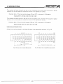
1
REVISIONS
<-.
%Themanualnumber
is givenonthebottom
Revision
Print Date
*ManualNumber
Aug., 1987
I6 (NA) 66132-A
First edition
Jan., 1989
I6 (NA) 86132-6
"Instructions for Strategic Materials" added
left of the back cover.
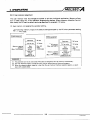
INTRODUCTION
Thank you for choosing the Mitsubishi MELSEC-A Series of GeneralPurposeProgrammqblt?Controllers. Please read this manual carefully so that the equipment is used to its optimum.
A copy of this manual should be forwarded to the end User.
.
1.1
1.2
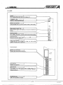
GONTENTS
"
r
;
*'
.I
.
2 SYSTEM CONFIGURATION
2.1Overall
2.2System
2.2.1
2.3General
2.4
.
.............................. 1-1 N1-6
How t o Use This Manual . . . . . . . . . ....................... .< ................ 1-2
1.1.1 A3HCPU features . . . . . . . . . . . . . . . . . . . . . . . . . . . . . . . . . . . . . . . . . . . . . . . . . .
1-3
Comparison between A3HCPU and Al(E). A2(E). A3(E)CPUs. . . . . . . . . . . . . . . . . . . . . . 1-5
'INTROOUCT+ON........................
............................................
2-1 N 2 - 9
Configuration .....................................................
Equipment .......................................................
Notes on compatibility with other ME LSEC-A series equipment
Description of System Configuration ...................................
..............
SystemDesignConsiderations ...............................................
2.4.1 Safety circuit ......................................................
2.4.2 Unit selection ....................................................
3. SPECIFICATIONS.
2.1
2.3
2-4
2-5
. . . . . . . . . . . . . . . . . . . . . . . . . . . . . . . . . . . . . . . . . . . . . . . . . .3-1
.
3.1General
Specifications. . . . . . . . . . . . . . . . . . . . . . . . . . . . . . . . . . . . . . . . . . . . . . . . . . . . .
3.2
A3HCPU Unit Performance Specifications .....................................
-
2-7
2.7
-2-9
.c
.
3-76
3.1
3.2
3.2.1 A3HCPU unit performance specifications ................................
3-2
3.2.2 User memory assignment
3.5
.
3.2.3
list . . . . . . . . . . . . . . . . . . . . . . . . . . . . . . . . . . . . . . . . . . . . . . . . . . . . . .3-10
3.2.4 Instruction list ....................................................
3.18
3.2.5 Timer processingandaccuarcy . . . . . . . . . . . . . . . . . . . . . . . . . . . . . . . . . . . . .-.3 - 3 5
3.38
3.2.6 Maximum counting speed of normal counter ............................
3.2.7Self.diagnosis
..................................................... 3.39
3.2.8Parameteranddevicerange
setting ....................................
3.40
3.40
3.2.8.1 File registers . . . . . . . . . . . . . . . . . . . . . . . . . . . . . . . . . . . . . . . . . . . . . . . . . . . . .
.............................................
.............................
(directhefresh)
switching
3-43
3.2.9 1/0control mode
3.2.10 Constantscan . . . . . . . . . . . . . . . . . . . . . . . . . . . . . . . . . . . . . . . . . . . . . . . . . . . .
348
3.49
3.2.1 1 Program types . . . . . . . . . . . . . . . . . . . . . . . . . . . . . . . . . . . . . . . . . . . . . . . . . . . .
3.2.1 2 Subsequence program . . . . . . . . . . . . . . . . . . . . . . . . . . . . . . . . . . . . . . . . . . . . . .
3.50
3.2.13 Notes on writing subsequence programs ................................
3-51
3.2.14 Subroutine program . . . . . . . . . . . . . . . . . . . . . . . . . . . . . . . . . . . . . . . . . . . . . . .
3.53
3.2.15 Interrupt program and interrupt counter. . . . . . . . . . . . . . . . . . . . . . . . . . . . . . . .3-54
.
3.2.16 Microcomputer program . . . . . . . . . . . . . . . . . . . . . . . . . . . . . . . . . . . . . . . . . . .3.59
3.2.1 7 Status latch. . . . . . . . . . . . . . . . . . . . . . . . . . . . . . . . . . . . . . . . . . . . . . . . . . . . . .
3.60
3.2.1 8 Sampling trace. . . . . . . . . . . . . . . . . . . . . . . . . . . . . . . . . . . . . . . . . . . . . . . . . . .
-3-60
3.61
3.2.19 Pause function . . . . . . . . . . . . . . . . . . . . . . . . . . . . . . . . . . . . . . . . . . . . . . . . . . . .
3.2.20 Step run . . . . . . . . . . . . . . . . . . . . . . . . . . . . . . . . . . . . . . . . . . . . . . . . . . . . . . . .
3.63
3.63
3.2.21 Remote run . . . . . . . . . . . . . . . . . . . . . . . . . . . . . . . . . . . . . . . . . . . . . . . . . . . . . .
3.2.22 Assignment of 1/0 numbers. .........................................
3.64
3.2.23 Entry code . . . . . . . . . . . . . . . . . . . . . . . . . . . . . . . . . . . . . . . . . . . . . . . . . . . .3.67
..
3.2.24 Print title entry . . . . . . . . . . . . . . . . . . . . . . . . . . . . . . . . . . . . . . . . . . . . . . . . . . .
3.67
3.3Power
Supply Unit Specifications . . . . . . . . . . . . . . . . . . . . . . . . . . . . . . . . . . . . . . . . . . .
3.68
3.3.1 Power supply unit specifications . . . . . . . . . . . . . . . . . . . . . . . . . . . . . . . . . . . . . .3-68
3.3.2 Selection of power supply unit . . . . . . . . . . . . . . . . . . . . . . . . . . . . . . . . . . . . . . 3-69
.
IB INA) 66132-A
I
f5:
L -
..................................................
.........................................
.......................................
....................
.............................................
...................................................
................................
............................................
...
i
.
-971
Base Unit Specifications
371
3.4.1 Main base unit specifications
3-71
3.4.2 Extension base unit specifications
372
3.4.3 Notes on the use of the.A56Bwd A588 extension bases
374
3.5
Extension Cable Specifications
375
3.6MemorySpecifications
i . . . . . . 3-75
3.6.1 Memory cassette specifications
375
3.6.2 IC memory specsifications
3.7
Fuse Specifications ......................................................
3-76
3-76
3.8
BatterySpecifications
3.4
....................................................
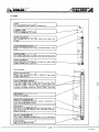
4.HANDLING
4.1
4.2
4.3
4.4
4.5
4.6
.
.......................................................
.....................................................
.........................................................
HandlingInstructions
4-1
4.1.1 Rnainunit
4-1
4.1.2 Memory (Memory cassette) ...........................................
4-1
4.1.3 Battery
42
Nomenclature
4-3
Memory Cassette Nomenclatwe . . . . . . . . . . . . . . . . . . . . . . . . . . . . . . . . . . . . . . . . . . . . .
4-5
Memory Cassette Preparation ...............................................
49
4.4.1 Memory i.c. installation
4-9
4.4.2 Memory protect switch setting
4.11
4.4.3 Batteryinstallation
4.12
4.13
Power Supply Unit
4.13
4.5.1 Nomenclature
4.5.2 Power
supply unit input voltage designation .............................
4.17
:.'4-18
Baseunits ...........................................................
4.6.1 Nomenclature ....................................................
4.18
4.6.2 Extension stage number assignment ...................................
4.21
..........................................................
...........................................................
..............................................
........................................
................................................
......................................................
.....................................................
5 LOADING AND INSTALLATION
5.1
5.2
5.3
5.4
5.5
. . 4 - 1 - 4.21
.......................................
51
hl
5-12
...................................................
51
InstallationEnvironment
52
Base UnitMounting . . . . . . . . . . . . . . . . . . . . . . . . . . . . . . . . . . . . . . . . . . . . . . . . . . . . . . .
5.2.1 Mountinginstructions .......................................
: . . . . . . . .5 2
5.2.2 Installation . . . . . . . . . . . . . . . . . . . . . . . . . . . . . . . . . . . . . . . . . . . . . . . . . . . . . . . .
53
5.2.3 PC generatedheat calculation . . . . . . . . . . . . . . . . . . . . . . . . . . . . . . . . . . . . . . . . . .
54
Installation andRemoval of Rack Mounted Modules ......................
. . . . . .5 6
Installation of Dustproof Cover . . . . . . . . . . . . . . . . . . . . . . . . . . . . . . . . . . . . . . . . . . . . . .
58
Wiring . . . . . . . . . . . . . . . . . . . . . . . . . . . . . . . . . . . . . . . . . . . . . . . . . . . . . . . . . . . . . . . . .
59
5.5.1 Wiringinstructions . . . . . . . . . . . . . . . . . . . . . . . . . . . . . . . . . . . . . . . . . . . . . . . . .
59
5-12
5.5.2 Power supply and grounding wirihg example.............................
.
.
6 PRE-START-UP ANDTEST PROCEDURES. . . . . . . . . . . . . . . . . . . . . . . . . . . . . . . . .6.1 m 6 - 2
6.1
6.2
Pretest Check List .......................................................
6.1
Test Procedure . . . . . . . . . . . . . . . . . . . . . . . . . . . . . . . . . . . . . . . . . . . . . .
:. . . . . . . . . . . .6.2
IB (NA) 661326
1. INTRODUCTION
1. INTRODUCTION
1. ,I~WODUGTION~.:'
i, ..
/MELSEC
.
.
ThisI'rnmkJal includes specifications, functions, and handling instructiohs for the A W C P U general. .
purpo3e programmable controller.
The M M C P U is, a high speed PC for use with standard A4eries .I& modulesand the majority
of the.&$eries special function modules, I t is programmed in the same way%as the other%A-Series
CPUs with some minor changes.
\
.
t
I
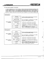
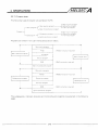
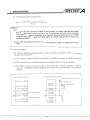
1. INTRODUCTION
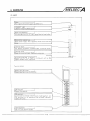
1.1 How to Use This Manual.
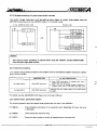
This manual is divided up intosections as follows:
-Section 2:
Section 3:
W p a t i b i l i t y o t pmgramming p e r i p k a k , special
and utility aftware packages.
functionunits
General informationon
system configurations.
Hardware, software and performance specifi-
caticins.
Definitions and explanations of A3HCPU
ware features.
,
-
soft-
Section 4:
Nomenclatures for A3HCPW and. associated
hardware.
Hardware preparation, switch settinge@.
Section 5:
installationinstructions,environmental
ations, power supply requirementsetc.
Section 6:
Prestart-up test and c h d procedures.
Section 7:
Troubleshooting. List and definitionsof
codes. Troubleshooting digital I/O\wiring.
Section 8:
Periodic maintenance and inspection
requitements. Battery and fuse replacement.
consider-
error
Appendices
The following manuals
may
also be required
A1 (E), A2(E), A3(E) CPU 1/0 unit user's manual
A l ( E ) , A 2 E ) , A3(E) CPU Programming manual
A3HCPU P21/R21 Data Link Unit User's M m a l
Data Link Unit User's Manual
In this manual the AGGPP, AGPHP and AGHGP are
referred to as GPP/PHP/HGP respectively.
.
.
.
1. INTRODUCTION
.
/
.
.
.
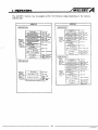
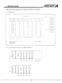
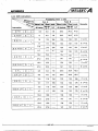
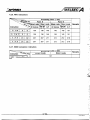
1.2 Comparison between A3HCPU and Al(E), A2(E), A3(E)CPUs
I
tI
II
Control
method
1/0 control
mode
I
Programming language
Use with MELSAP language
1
Number of
inStNCtionS
Sequence instruction
I
Number of 110 poifits
I
I
Language decbkted
sequence control
(Relay s y w i , logic
y m b o l i c Ienguege)
I
No
I
Direst m a :
I
0.2 to 2 IWstep
0.2 to 0.4 pS/step
Refresh mode:
256
2048
Can be set between 10 and 19Oms
in 1Oms increments.,
Watch dog timerWDT)
2o(ms only
I
failure
power
Weight kg (Ib)
I
I
Memory capacity Max. 144K bytes
132 types
I
$32.
Within 2Oms
I
0.9 (1.98)
1
Within
1.65 (3.63)
Main sequence program
Max. 6K steps
Subsequence program
Max. 30K steps
Microcomputer program
Max. 58K bytes
(
"Fs!
Link relay ( 6 )
I
0.7 (1.54)
parameters
,
0.8 (1.76)
de^^,$^^^ 1
in the parameters
(L1000 to 2047)
Unavailable
I
I
I
d
t
lOOms timer: set time 0.1 to 3276.7 sec (TO to 199)
10ms timer: set time 0.01 to 327.67 sec (T200 to 255)
l O O m s retentive timer: set time 0.1 to 3276.7 sec
256
256
Normal counter:
set value 1 to 32767 (CO t o 255)
count:i
Specifications
~ \ ~ ~ , " ~ u ~ t &(co
7 6to7255)
interrupt program counter:
set value 1 to 32767
*Counter used in interrupt program
Interrupt
value to 32767
7 G i K G 5 5 uwc specified)
Counts tha number of interrupt signals
received.
1024 points (DO to 1023)
1024 points (DO to 1023)
Link register (W)
1024 points (WO to 3FF)
1024 points (WO to 3FF)
Annunciator ( F )
i
256
Data register (DI
I
~
Max. 30K steps
256
Number of points
Counter (12)
I
1024 points (BO to 3FF)
1024 points (BO to 3FF)
Specifications
I
I
s t e p s Max. 30K bytes Max. 14K
Unavailable
Number of points
Timer ( T )
I
Max. 10K bytes Max. 26K bytes Max. 58K bytes
(LlOOO to 2047)
0 point
(defaults to no value) '
2048
2Oms
Internal relay (M)
IS)
I
Can be set between 10 and 2 0 0 0 m r
in l O m s increments.
Max. 16K bytes
Step relay
'-
A3ECPU only
Max. 30K steps
Latch relay ( L )
I
1.25 to 2.25 pShtep
I
Max. 144K bytes
Program
capacity
I
1
2 2 ..t L
types 131
Constant scan function
(Program start +.qpecified intervals)
Iinstantaneous
Allowable
Yes
132 types
I
1
I
~
Language dedicated t o sequence control
(Relay symbol,logic symbdic Iangume)
- -
-
22 types
I
Basic instruction
Processing speed
(Sequence instruction)
.~~
Stored
Drwram.
. . r e.i a t e d oDeration
A l , A2, A3CPUs direct
A l E , A S , A ~ E C P U refresh
J
Refresh/direct (selectable)
I
to
11
Stored
program,
repeated
operation
I
(FO to 255)
points
256
I
points
256
255)
(FO to
I
I
I
I
I
.
-
., .. _,
.
1-5
IB lNAl €6132-A
i
1. INTRODUCTION
ABHCPU
File register ( R )
comments
,-
of
Max. 4032
Number
I
latch
I
function
switch
Offline
Status
I
function
F number indication
Annunciator display function
1
Unavailable
I
1
Available
( Y , M , L, B, F )
I
Available
Available
Output mode switching
at change from STOP to RUN'
Available
Available
7
I
Print title
~~
~~
Available
~~
Software I/O assignment
,
1
I
Using GPP/ PHP/HGP
F: "
*
F number
indiehion
Unavailable
Available
Entry code
I
Available
Operation mode switching
during error occunence
~~
I
1
UnavailaMe
Available
setting contactrunlpaute
Remote
Ientry
Availabla-
Max. 4032 points
I
4"+;*"I:...ik+,
Available
Available
Using GPP/PHP/HGP
I
I
.F'
'.
.I
.
.
.._
..
.
.
1-6
.. IB INAI €6132-A
1. INTRODUCTION
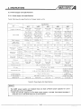
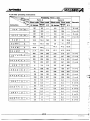
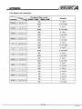
2.2 System Equipment
I
TYPI
Unit
I
I
1
tIcor:
I
MHCPUP21
A3MCA-O
.
o - 0 0 0
o--
e)
Without IC-RAM mernorv
0 0'0
bvtes h e x . 30K s t e m )
I
lemory
IC-RAM
I
I
'4KRAM
'4KROM
EP-ROM
8KROM
1
I
I
bytes (max. 60K steps)
I
I
8Kbvtestmax.3KrtbDs)
8Kbytes(max.3K
16K
bvtes
Imax.
Remarks
i
0
A 3 H C P U ~ 2 1 Far coexWdata link
(Master, local selectable)
For optical data link
(Master, local w l h l
I
t
Program
30K steps,
I/O p o t n t s : 3048 points
M, L total:2048points,
T : 266 poims
C: 256 points, D: 1024 points
A3HCPU
sw e m
1
Description
cawty:
CPU unit
Applimlbl
- beMemory
cassatte to
arranged separately.
0
O
I
steps)
7K stead
-.
O /
~~
TaMe 2.1 L i s t of Equipment
*With two memory
sockets
ABMAC-0 can be
loaded with IC-RAM
or EP-ROM memory.
ASMCA-2 to -18can
be loaded with only
EP-ROM memory.
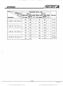
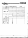
1. INTRODUCTION
2.2.1 Notes on compatibility with other MELSECd sariesequipwt
.
,
1) All digital I10 modules are curnpat-wewith the A3HCPU.
2) All special function units (includinganalog I/O modules) are compatible with the A W W U with
the following exceptions:
a) AJ71C13
b)
AD57
c) AD58
d)
AJ71C24
e) AD51
Versioq
with
. .
Incompatibb.
Incompatible.
Incompatible.
Veroiqty with
compatible.
compatible.
H @receding the
serialnumber,
as shown below, are
H preceding the serial number, as shown below, are
I
58
Compatible with
3) The following microcomputer software packages are incompatible with theA3HCPU:
a) SWOC-UTLP-PID
b) SWOC-UTLP-FNO
C) SWO-AD57P
4) The followingrestrictions
A3HCPU:
a) AGGPP/AGPHP
b) AGHGP
c ) A7PU
d ) AGWU
Incompatible.
Incompatible.
Incompatible.
apply to the use of peripheralprogrammingequipment
with the
Use software package SWSGP-GPPAL?!:I-1/2, or subsequent versions.
Use software packageSW3-HGPAI:IKI-1/2, or subsequentversions.
Versions with H preceding the serialnumber, as shown below, are
compatible.
Versions with H preceding the serial
number,
as shown below, are
compatible.
A7PU
I
DATE
H
702 AC
I
Y
2-4
IB INAl 86132-A
1. INTRODUCTION
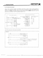
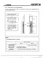
2.4 SysQm Design Considerations
_.
2.4.1 Safety circuit
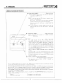
Note the following:
On switching on the PC power supply, there is a short but fin$&time before the DC levels
operate normally. The same
reach their operating values. During this period, the unit will
applies when the power is cut as the D€ levels d r 6 below thdkbperating values. The following circuit will overcome any problems which may arise in output control due t o this phenomenon.
i
i
1
I
2-7
I
IB INN €81324
I
f
A
1. INTRODUCTION
I System design circuit example 1
All AC
POWER
TRANSFORME
POWER
Mixed AC and DC
TRANSFORM
FUSE
1
*5
**1
recommended
*2
/*3
*\ MC
TC
*A
1
' 1 : Runhtop circuit interlocked withR A l (run monitor relay)
'2: Battery lowalarm
'3: R A I switched on by M9039 (run monitor relay)
' 4 : Power to outputequipment switchedoff when stop signal given.
*5: Input switched when power supply established.
'6: Set time for DC power supply to be established.
' 7 : On when run by M9039
'8: Interlock circuit as neccessary.
The power-on procedure is as follows:
For AC
1)
2)
Switch on power.
Set CPU t o RUN.
3) Switch on the start switch.
4 ) When the magnetic contactor (MC) comes in, output equipment is powered and may be driven from the program.
For ACJDC
1)
2)
Switch on power.
Set CPU t o RUN.
3) When DC power is established, RA2 turns on.
4 ) Timer (TM) times out after the DC power reaches 100%.
(The set value of TM should be the period o f time from when RA2 switches on t o the establishment of 100%
DC voltage. Set the s e t value t o approximately 0.5 seconds.)
5) Switch on the start switch.
6) When the magnetic contactor (MC) comes in, the output equipment is powered and may be driven by the
program.
2-8
IB lNAi 66132-A
1. INTRODUCTION
2.4.2 Unit selection
(1 Power supply unit
(a) Select the power supply according to the 5 V P C current requiredin the systw.
If the capacity is to6zmall, there will be 8 &qp in the DC 5V, resulting i n % W shutdown,
erroneous I/O signals, etc.
(b) The 5V DC power to an A556 or A586 extension base, is suppJid.;from the power supply
on the main base unit. WhenUsing either of these extension bases'ensure t h a t the power
supply selected has sufficient capacity for bothbases.
(c) When using the 24V DC output from the
is never exceeded.
power supply ensure thqt the current capacity
? r
(d) When using an A66P power supply unit, instalh it a t the right e,nd,of thebase unit.
The unit located t~ the left of the A M P must be selected according t o Section 3.3.2 (3) as
the 24V DC output from theA66P varies according to this unit,
(e) Power supply specifications can be, found in Section 3.3.
(2) Extension base unit
For base units
(A556,
A5861
not
requiring
their
own
power supply unit,
5V
DC is supplied
from the power supply unit in the main base unit via the extension c a ~ g as
, described in (2) (a)
above. In this case, a voltage drop occurs
over the extension cable SD thatthe voltage at the
receiving end is less than that at the source end.
Since a t least 4.75V DC i s required a t the receiving end, it is neccessary to select the base unit
so that the voltage does not drop to less than 4.75V DC. For information on selecting the A556
or A586, refer to Section 3.4.3.
,
7
!
I
i
For information on 1/0 units, refer to the A l , A2, ABCPU I/O Unit User's Manual.
I
f
c
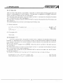
3. SPECIFICATIONS
3.1 General Specifications
Itam
1
I
Spedfications
Operating ambient
temperature
0 to 55OC
Storage ambient
temperature
-10 to 75OC
Operating ambient
humidity
10 to 90%RH, non-condensing
Storage ambient
humidity
10 to 90%RH, non-condensing
Frequency
Conforms to JIS C 091 1
Vibration resistance
I
I
10 to 55Hz
-
0.075mm
55 to 150Hz
lg
-
Sweep Count
10 times
" ( 1 octave/minute)
Shock resistance
Conforms to JIS C 091 2 ( l o g x 3 times in 3 directions)
Noise durability
By noise simulator of 1OOOVpp noise voltage,
1p.s noise width and 25 to 60Hz noise frequency
15OW AC for 1 minute across AC external terminals and ground
m v AC for 1 minute across DC external terminalsand ground
Dielectric withstand
voltage
Insulation resistance
Grounding
Operating ambience
-
Acceleration Amplitude
I
5MS2 or larger by 500V DC insulation resistance tester across
AC external terminals and ground
Class 3 grounding
(Grounding
not
neccessary for PC operation)
Free of corrosive gases. Dust should be minimal.
Cooling method
Self-cooling
Table 3.1 General Specifications
One octave marked indicates a change from the initial frequency to double or half frequency. For example, any
of the changes from 10Hz to 20H2, from 20Ht to 40Hz, from 40Hz to 20Hz, and 20Hz to 10Hz are referred to as
one octave.
3-1
I8 (NA) 66132-A
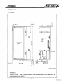
3.2 A3HCPU Unit Performance Specifications
3.2.1 A3HCPU unit performance specifications
Items marked *. in the table are enabled, or their ranges assigned, in the PC parmeters using the
peripheral quipment (PU, GPP, PHP or HGP, but partly restricted in the case of PU). 'For details
of parameter setting, refer to Section 3.2.8 "Parameterandrange
setting". The following table
shows default settings:
Item
I
I
Performance
I
I
Control system
Stored
repeated
program,
I
1/0control method
(I/Ocontrol
setting)
Direct/refresh method
Sequence instruction
22 types
Basic instruction
132 types
Application instruction
107 types
Direct mode
Processing
speed
Sequence instruction 0.2 to 2 p/step
Refresh mode
I
Constant scan
(program start at specified intervals)
Memory
capacity
and
memory type
II
Language dedicated to sequence control
(Combined use of relay symbol type, logic symbolic language)
Programming language
Instruction
operation
Sequence instruction 0.2 to 0.4 p/step
Can be set between 1Oms and 19Oms in 10ms
increments
Memory capacity
Max. 144K bytes
Memory type
(Memory cassette type)
Memory cassette A3MCA-0 to A3MCA-18
(For memory cassette details, refer to Section 3.8.)
* Main sequence program capacity
6K steps
(Can be s e t to max. 30K steps)
1/0 points
2048 points
* Internal relay (M)
* Latch relay (L)
1000 points (1000 bits)
I
1048 points ( 1048 bits)
I
*Step relay (S)
Link relay (B)
Defaults to no value.
Used in the same manner
as theinternal relays
1
The number of M+L+S
devices is 2048
t
BO to 3FF 1024 points (1024 bits)
Table 3.2 Performance Specifications
-
3-2
IB INN 66132-A
Item
Number o f points
I
I
Performance
256 points
TO to 199, 1 0 h s timer:
setting time 0.1 t o 3276.7 sec
*Timer
Specifications
* Counter
Number of points
OSet values can be changed
by parameters.
OTimer accuracy
t 2 scan times
, -1 scan time
T200 to255, 1 ( x n s timer:
setting time 0.01 t o 327.67 sec
I
I
Specifications
1 o O m s retentive timer:
depending on setting
(setting time 0.1 t o 3276.7 sec)
256 points
CO t o 255, normal counter: setting range 1 t o 32767
(C224 t o C255 may be used as interrupt counters. See Section 3.2.15.)
Data register ( D l
DO to 1023, 1024 points (16 bits per word)
Link register (W)
WO to 3FF, 1024 points (16 bits per word)
Annunciator ( F )
FO t o 255, 256 points (256 bits)
I
* File register ( R )
Depending on setting (Max. 8192 points)
AO, A l , 2 points (2 words)
Accumulator ( A )
Index register (V, 2 )
Pointer (P)
(I)
Pointer
interruption
for
Special relay (M)
I
I
I
V,
PO t o 255, 256 points
IO to 3 1 , 3 2 points
M9000 to 9255,
256
* Status latch
Set in parameters (Max. 24K bytes)
*Sampling trace
Set in parameters (Yes.
* Comment
* Subsequence program capacity
* Latch
I
Set in parameters (Max. 30K steps)
L1000 t o L2047 (1048 points)
* Link range
Set in parameters
* Remote runlpause contact
Set in parameters
* Operation mode a t the time oferror
I
1/0 error : STOP
Software instruction error : CONTINUE
F number display
*Annunciator display mode
* Entry code
* Print title entry
mode
. . . .8K bytes)
Set in parameters (Max. 4032 points)
(power failure compensation) range
+. RUN
output
points (256 bits)
D9000 to 9255, 256 points (256 words)
Special register ( D l
*STOP
Z,2 points (2 words)
1
I
Output data a t time of STOP is restored.
Set in parameters
I
Set in parameters
Table 3.2 Performance Specifications (Continued)
3-3
IB (NAI 66132-A
Item
Performance
* 1/0 assignment
The number of 1/0 points allocated to each dot is dictated by the
individual l/O units used. An emptyslot mupies 16 points.For
details, refw toSection 3.2.22.
* Selfdiagnoftlc functions
M o c y error dewthan, CPU error detection, 1/0 error detection,
Watch dog error monitor (watchdog timer 2 0 h s only)
battery error detection,etc.
(For deteils, refer to Section 3.2.7.)
__
At power-on, a t power restoration
after power failure
Automatic restart when “RUN” switch is moved t o ON position
(Initial start)
I
IC-RAM backup
I
Break point setting and run per instruction can be executed using
peripheral equipment (not PU) connected to the CPU unit.
Step run
I
Other
functions
*
I
lctequpt program can be run in response to a signal from
Interrupt processing
I
rupt unit or bya constantcycle interrupt signal.
an inter-
Data link
* Microcomputer mode
Depending on setting
power failure time
Within 2Oms
Current consumption (A)
3.0
Weight kg (Ib)
0.9 (1.98)
External dimensions
mm (inches)
250 x 79.5 x 121
(9.84) (3.13) (4.76)
r
1
Items marked in this table are set in parameter mode using any of
the peripheral programmingdevices.
Parameters
I
By lithium battery
Battery guaranteed for 5 years.
For total power failure guarantee time, refer to Section 8.3.
t
Table 3.2 Performance Specifications
POINT
MELSAP (MELSEC Flow diagram programming language) cannot be used to write A3HCPU
programs.
I
.
.
3-4
IB (NAI €6132-A
ct
4
i
*
1
3.2.2 User memory assignment
The user memory may be arranged as required to suit the individual application. Memory allocation is made using any of the peripheral programming devices. Where memory allocation has not
been made, the PC uses i t s default settings as described in paragraph (1 ) below.
(1 ) User memory not assigned by parameter setting,
The following memory maps are the default settings adopted by the PC when parameter setting
has not been made.
1
I
I LROM operation J
RAM ODeration I
Parameter
T/C set value
Memory cassette
capacity
(Max. 144K bytes)
REMARKS
I
Main
sequence
program
memory
cassettes
IA3MCA4 to 18.1
3K bytes
K
1 bytes
I
I
Parameter
I
I
ROM memory
capacity
(Max. 64K bytes)
I
I
Max. 6K
I
steps
I
( 12K bytes) I
I
I
,
I
Memory cassette
capacity
(Max.144Kbytes)
3K bytes
1K bytes
Main
sequence
program
Max. 6K
steps
(12K bytes)
for memory
cassettes
I
1
(1) The parameter and T/C set value areas (4K bytes) are assigned t o the user memory automatically.
(2) The main sequence program includes the main routine, subroutines and interrupt programs.
(3) When the sequence program capacity is less than the user memory (memory cassette) capacity, a vacant
area is l e f t as shown above.
,
3-5
18 (NAI 66132-A
(2) User memory assigned in parameters.
In ocder to dnable some of the PC functions, memory areas must be allmated acmrding to the
function required using any of the peripheral programing devices (use of thaPU, h o w e r , is
limited). Memory areas to which allmation may k
m
&
e are shown below. MW-that the total
amount of memory usedmust not be greater than the capacity of the memory cassette used.
I
I
Parameter
4K bytes are always required from the user memory
area for storing the parameter settings.
T/C set value
Microcomputer program
Memory cassette
RAM area
1 1
:;:7
Can be set between 1 and 30K steps (2 and 60K
bytes) in 1 Kstep (2K byte) increments.
1
Data area
File register
No (OK byte) or yes (8K bytes) can be selected.
No (OK byte) or yes (8K bytes) can be selected.
No (OK byte) or yes (bytes set for file registers)can
be selected.
Canbe set between 0 and 16K bytes (0and 8192
points) in 2K byte (1024 point) increments.
Canbe set between 0 and 64K bytes (0and 4032
points) in 1K byte ( 6 4 point) increments.
File register
Comment
I ROM operation 1
Parameter
Memory cassette
ROM area
4K bytes are always required from the user memory
area for storing the parameter settings.
TIC s e t value
Sequence program
1
Microcomputer program
I :a I
~
Sampling trace
I
-1
Memory cassette
RAM area
1
1
i
I
Data area
File register
File register
'
Canbe set between 1 and 30K steps ( 2 and 60K
bytes) in 1K step (2K byte) increments.
No (OK byte) or yes (8K bytes) canbeselected.
No (OK byte) or yes (8K bytes) can be selected.
No (OK byte) or yes (bytes set for file registers) can
be selected.
Canbe set between 0 and 16K bytes (0and 8192
points) in 2K byte (1024 point) increments.
Canbe set between 0 and 64K bytes (0and 4032
points) in 1 K byte (64 point) increments.
3-6
IB (NAJ €6132-A
The A3HCPU memorymay
cassette used.
be assigned within the following rangesdepending
onthememory
A3MCA-2
1 RAM operation 1
II
Memory
cassette
capacity
Max. 16K
bytes
(IC-RAM
memory
Parameter
I 3K bytes
Parameter
3K bytes
1 K byte
Max. 6K steps
(1 2Kbytes)
Max. 10K bytes
1 K byte
Max. 2K steps
(4K bytes)
Max. 2K bytes
)I1
11
Unused
Sampling trace
File register
~ROM
operation
I
Parameter
1.
!I
5K bytes
8K bytes
Max.
byte'
10K
(5120 points)
Max. 10K byte!
(576 points)
1 R O M operation I
ROM
memory
capacity
Max. 64K
bytes
(32K steps)
Memory
cassette
capacity
Max. 16K
bytes
3K bytes
bytes
3K bytes
1K byte
W X . 30K steps
(60K bytes)
Max. 58K bytes
1 K byte
Max. 5K steps
(10K bytes)
Max. 8K bytes
5K bytes
8K bytes
Max. 16K bytes
Max. 16K bytes
bytes
(8192 points)
Max. 16K bytes
(960 p o ~ n t s )
3-7
IB INAI 66132-A
1
A3MCA-4
A~MCA-~
I RAM operation
m
r
y
'
cassette
capacity
Max. 32K
bv
bytes
.
I RAM operatioh]
3K bytes
1K byte
Max. 14K steps
(28K bytes)
Max. 26K bytes
1K byte
Max. 1OKsteps
(20K bytes)
Max. 18K bvtes
3K bytes
1K byte
Max. 30K steps
(60K bytes)
Max. 58K bytes
1K byte
Max. 26K steps
(52K byte9
Max. 30K bytes
5K
5K bytes
8K bytes
8K bvtes
Max. 24K bytes
Max. 24K bytes
Max. 16K bytes
M a x . 16K bytes
Max. 26K bytes
Max. 58K bytes
L36_4-~p_oi
(8192 points)
ROM
memory
capacity
Max. 64K
bvt-
(32K step3
Memory
cassette
capaclty
Max. 32K
bvtes
p r
'-
(8192 points)
2sL -
3K bytes
1K byte
Max. 30K steps
(60Kbytes)
Max. 58K bytes
1K byte
Max. 13K steps
(26K bytes)
Max. 24K b v t e s
memory
program
Memory
cassette
capacity
Max. 64K
bytes
5K bytes
8K bytes
I
+1
3K bytes
1K b y t e
Max. 30K steps
,(60K bytes)
Max. 58K bytes
1K byte
Max. 29K steps
(58K bytes)
Max. 56K bytes
i
i
5K bytes
Unused
Samphng trace
8 K bytes
Max. 24K bytes
M a x . 16K bytes
(8192 points)
Max. 64K bytes
Max. 16K bytes
18192 polntsl
M a x . 32K bytes
(1984 polnts)
(4032 points)
f
I
3.8
r
1
IB lNAl 66132-A
I
1I
ABMCA- 18
A3MCA- 12
j
RAM operation
RAM operation
3K bytes
1K byte
Max. 30K steps
Unused
/I 1-1
I
ROM
II
File register Max. 24K bytes
Max. 16K bytes
(8192 points)
Max. 64K bytes
14032 Dointr)
Parameter
--__ -_
I t 3K bytes
capacity
capacity
Max. 64K
bytes
(32K steps
I
Memory
caSsette
S i Z K
bytes
‘FIl
II
Ilnused
cassette
I
bytes
Comment
64K
Max.
bytes
Max. 24K bytes
I’
\I
Comment
--- --
Max. 16K bytes
(8192 points)
11bytes
64K
Max.
- 14032 mints1
J
3K bytes
1K byte
Max. 30K steps
(60K bytes)
Max. 58K bytes
1K byte
Max. 30K steps
(60K bytes)
Max. 58K bytes
5K bytes
0K bytes
8K b
by
y tt e
e
8K
File register
REMARKS
5K bytes
8K bytes
File register
memory
Memory
cassette
capacity
Max. 144K
bvtes
5K bytes
II
3K bytes
1 K byte
Max. 30K steps
(60K bytes)
Max. 58K bytes
1 K byte
Max. 30K steps
(60K bytes)
Max. 58K bytes
Parameter
1K byte
Memory
cassette
capacity
Max. 96K
bytes
1
Max. 24K bytes
Max. 16K bytes
(8192 points)
Max. 64K bytes
(4032 points)
Max. 16K bytes
(8192 points)
(4032 points)
I
(1) 4K bytes of user memory are always required for parameter and timerhounter set value storage.
(2) ”sequence program” includes subroutine and interrupt programs.
(3)Note the following when assigning memory protect areas:
Parameter, sequence program and subsequence program areas are assigned, in order, t o the beginning
of t h e memory map.
Comment, file register, status latch, and sampling trace areas are assigned to the end of the memory
map as indicated above. There is therefore an unused memory range between the two areas. Memory
protect should therefore be assigned t o the first part ofthe memory map.
(4) The maximum values for items shown above indicate the maximum value for that item taken on its
own.
(5) When mixing ROM and RAM, any item other than the sequence program may be assigned to RAM.
(6) The capacities shown above for microcomputer and submicrocomputer programs are the maximum
possible with thecorresponding sequence program areaset t o 1K steps (=2K bytes). Sequence
program + microcomputer program must be 60K bytes.
<
3 -9
IB (NAJ 66132-A
3.2.3 Device list
Thissectiongives the namesandaddressranges
of the devices availableon the A3HCPU. Items
marked* in the table are enabled, or their ranges assigned, in the PC parameters using the peripheral
equipment (PU, GP?, PHP or HGP, butpartly restricted in the case of PU). For detairs otparameter
setting, see Section 3.2.8 "Parameter and range setting."
Points
Remarks
X, YO to 7FF
(X, Y total 2048 points)
X, Y numbers are in
Device
X
Input
~
Y
I
I
Output
Special relay
*
1 1
Internal relay
*
L
Latch relay
*
I
I
I
1
s
F
I
1
I
T
Step relay
Annunciator
looms timer
I
1
j
I
I
M9000 to 9255 points)
(256
MO to(1000
999
D
II w 1i
R
IA I
V
1
~
I
ber of
c:S=2048
Set in parameters
DDOOO to 9255 (256 point)
Link register
WO to 3FF (1024 points)
I
I
K
Decimal constant
H
Hexadecimal constant
II
POINT 1
I
I
There are 256 points
of timers and counters,
respectively.
I
Set in parameters (0point)
~
2 (1 point)
I
I
I
V (1 point)
(8
NO to 7
W numbers are in
hexadecimal
I
points)
(2
AO, A1
~
Index register
Pointer
interruption
for
,
(0point)
Special register
Pointer
...
CO to 255 (256 points)
DO to 1023 (1024 points)
I P I
M+
Set in parameters (0point)
Data register
Nesting
___
T200 to 255 (56 points)
Interrupt counter
Accumulator
~~
-
TO to 199
points)
(200
Counter
File register
num-
FO to 255 (256 points)
1Oms timer
I N 1
II1
I
I
Set in parameters (0point)
~~~
Z
points)
L1ooo t o 1024 ( 1024 points)
1 Wms retentive timer
C
hexadecimal
I
levels)
I
PO topoints)
255 (256
I
IO t o 131points)
(32
K32768 to 32767 (16-bit instruction)
K2147483648 to 2147483647 (32-bit instruction)
HO to FFFF (16 bitinstruction)
HO to FFFFFFFF (32-bit instruction)
Table 3.3 Device List
I
The function of step relays (S) is identical to that of internal relays (M).
3-10
. .
IB (NA) €6132-A
r
( 1 ) Special relay list
The special relays are internal relays with spwial functions, They are mostly used as contacts
to provide interlocks, timing pulse chains, etc. Table 3.4 shows the special relay list.
M9200 and following are used in conjunction with theMELSEC-NET data link system.
Number
I 2- I
I
I
1
1
.
II
I
I
I
I
I
k'9002
k'9005
~'9006
hb007
Name
I
Fuse blown
I
Battery low
I
I
It0 unit
Error
ON:
error
verify
detection
1
OFF:Normal
ON: Fus.?biown in an
1/0 module
1
I gLF:
OFF: AC supply normal
ON: AC is down
Battery low
OFF:
Normal
latch
ON:
Annunciator
detection
*1
Operation
error
Error
M9011 ON:
flag
M9017
M9020
M9021
M9023
M9024
II
I
I
1
Battery
low
No error
Turned on by a power failure of within 10ms. Reset when PCCPU
is reset.
0
Turned on when battery voltage drops below that specified.
Turned off when battery voltage i s restored.
0
Turned on when battery voltage drops below that specified.
Remains on after battery voltage is restored.
0
Turned on byself-diagnosed error.
OFF: No annunciator
detected
ON: Annunciator
detected
.Turned on when OUT F or SET F instruction is executed.
Switched off when all annunciators ( F ) are switched off.
OFF:
No
0
Turned on by an application instruction processing error.
Remains on after normal status is restored.
0
Carry flag used i n application instructions.
error
@Clearsthe data memory(otherthan
special relays and special
etc. when M9016
registers) in remote run mode from computer,
OFF: Ignore
clear flag
ON:
Output
clear
Data memory
Clears the unlatched data memory (other than special relays and
special registers) in remote run mode from computer, etc. when
M9017 i s on.
User timing
clock No. 0
User timing
clock
No.
1
I
I
0 Scan dependent clock pulse.
0After poweronor
CPUreset, thedutclockcontacts
On and off periods are specified i n the
instruction.
-n
clock No. 2
User timing
clock No. 3
User timing
clock No. 4
M9032
1 second
clock
M9034
Turned on when one or more output unitfuses have blown.
Remains on after normal status i s restored.
clear
0.2 second
clock
I
I
low
ON:
Output
M9031
M9033
0
.Turned on when an 1/0 unit is removed from,or added to the
system while the power is switched on. Remains on after normal
status is restored.
OFF:Normal
Self-diagnostic
OFF:
Error ON: error
M9009
Details
Description
2 second
clock
1 minute
clock
I+++
n l scans
1
-
0.1
seconds1 seconds
o.l
DUTY
I
nl
n2
are open.
M9020
*Time dependent clock pulse: 0.1 second, 0.2 second, 1 second,
2 second, and 1 minute clocks.
@ N o t scan dependent (i.e. will be switchedduring scan if corresponding time has elapsed).
0 Starts when power is turned on or CPU is reset.
0.5
seconds seconds
loa5
I
secnndc
s30 e
d
zondz
Table 3.4 Special Relay List
3-1 1
IB (NAl €6132-A
I
I
Number
Name
I
I
bription
~_____
Details
as dummy
contacts
forinitialization
and
application
ructiqw,
$%36
arid )3;$037 are turned on and off indepwdently of the
&?switcH
on'thc
. .
q h q n m d w n d i n q o n t h gppfivh Wsition.
8 and M 9 are d t c h e d off If the key swlfch isfn'STOP
position.
M9038 is switched off (on for one scan onlv) and M9039 switchon(offfor
one scan only) ifthekey&itch
is n o t in STOP
position.
.Used
rv
fl8.andm
MbR
Q
M9039
RUN flag (off
ON
only for 1 scan :
M9040
PAUSE enable
coil
M9041
.
PAUS@M u s
,
Stop status
OFF: During stop
ON : Otherthan
canted3
Sampling tr=
complete
I
Sampling trace
1
trace
I
M9051
1
*When RUN key
witch is a t PAUSE position orremote
contact has tuon and i f M9040 is on, the PC enters PAUSE
mode and M9041 i s turned on.
,
stap
OFF:During=mpting
trace
' ,
ON: Samplingtmte
complete
OFF: Trece
inaceiue
ON: Trace actlve
I
o F F : Sampling traCe
oN: Sampling trge
witching
Main program
M9056 OFF:p,
Other
I set than
request
,
OFF: Decode function to
7-segment display
data
ON: Partial refresh
function
*The SEG instruction function is changed byswitchingM9052
onloff in the sequence program.
ON:
.Turned
P, I set request
P, I set
request
ON:
During P, I set
-request
OFF: Except during P, I
set request
M9057
Subpidgram
P, I set request
M9058
Main program
P, I set
complete
Pulsed on completion
Subprogram P, I
set completion
Pulsed on completion
of P, I setting
'2
M9084
Switched on during sampling trace.
.Sampling trace is startedbyswitchingon
M 9 w 7 in theprogram.
M9047 is automatically
switched
on
if sampling is started from
the GPP. By turning off "7,
sampling trace i s stopped,
I
M9059
,unecl un ru
the specified
Reset when
. '
M9055
Status
latch
OFF:
Not
complete
Complete
instruction.
ON: flag
complete
!
.
CMG instruction
ON:
Disable
disable
OFF: Enable
SEG instruction
M9052
1
I
I
~~~
OFF:PAUSE d&Ibd
ON: PAUSE enabled
OFF:Duringpaur).
ON: Omerthan pauao
oorreect
M9043
M-
1 scan
afterrun)
M9042
I
- _.
mu.
Error check
of P, I setting
OFF: Checksenabled
ON: Checks disabled
on when status latch is completed.
Turned
off by reset
C
Provides P, I q t requestafter completion of program correction
when correction of the,qthergrogram (for example subprogram
when main probram i s being run) is made during run.
Turned off after setting is complete.
.
, 0
Pulsed on after c o m p w o n
I
1
of P. I setting.
.Specify whether the YOllowlng errors are to be checked or not
after the END instruction is executed (to reduce END processing
time):
. Fuse blown
1/0 unit verify error
Batteryerror
i
.
.
I
I
Table 3.4 Special Relay List (Continued)
c
3-12
I
+
i
*
IB INA) 56132-A
f
POINT
*
(1) S m a l relays marked 1 above, are a
lW
h
d "on" and will remain on after normal status
is restored. S w i M then off as follows:
1) From the user program
Use circuit
the
shown on the right and turn on
the reset command contact to clear the special
relay M.
Reset command
RST M - 0 4
-$-
Specify the device to be reset.
2) From the peripheral equipment(PU,GPP,PHP
or HGP)
Use the test function to forcereset the device. For the operation procedure, refer to
the appropriate manual.
3) RESET the PC CPU using the key switch. Thiswill reset the special relay.
(2) M9084 marked *2 is switched on/off in the sequence program.
3-13
18 I N N 661324
. .
.
(2) Special register list
data registers with spedal functions: Data should not kwittei.l to
these registers (except those marked * in the table).D a t a mav bemad ftom th8)spedat registers
and used as appropriate imthe program. Table 3.5 shows the special register list.
D92QO a@?foHowing are used in conjunction with the MELSECNET data link system.
The sp&t~;registem.are
..
I
Number
I
Name
I
Data
I
D9000
Stored
I
Lowest unit number
lobation with blown fuse
I
Explanation
0
I h c a t e s the he&: 110
&
e
nof
th6 l o w e s t I/O unit number in
which tho fuse hwjblow% Jika the hWdec-1 monitor function
on the peripheral equipment to read the data.
(Cleared by resetting D9100 t o W107 t o 0.)
I
Indicates the head I/O address of the lowest 1/0 unit number for
vVhkh
t I 0 onlt verify wrar.has been detectlcl k u r a of error:
0
Lowest unit number
location with 1/0
verify error
l/O unit
D9002
verify error
0
I
.D9008
I
Selfdiagnostic
error
I
Self-diagnostic
number error
I
0
gn
addition or removal of an 1/0 unit while the power is on). Use the
hexadecimal monitor function on the peripheral equipment toread
the data.
(Cleared by resetting D9116 to D9123 to 0.)
1 is added each time the input voltagedrops to 80% or less of
rated while the CPU unit is operating, and the value stored in BIN.
Records the self-diagnosed error number.
Records the number (in BIN) of the earliest annunciator coil (F)
to be switched on by1 - 1
or
0 09009 can be cleared by executing the
or m
j
CPU front. If
instructionor
pressing INDICATORRESETon
another F number has been detected, the clearing of 09009 causes
the next number to be stored in D9009.
0
D9009
Annunciator
detection
Earliest annunciator
number detected
D9011
Error step
Step number
location of
operation error
0
r
+
,
Records the step number (in BIN) a t which an application instruction processing erroroccured.Errordatacannot
be overwritten
until special relay M9011 i s reset by the user program.
Table 3.5 Special Register List
..
.,
.
3-14
IB (NA) 66132-A
V
/MELsEC-A
-
3. SPECIFICATIONS
Number
Name
Stored Data
D9015
CPU operating
status
Operation status
of CPU
Explanation
Theoperating
below:
status of the CPU is stored i n D9015 as shown
t
CPU Operating mode
0
1
2
*PAUSE
3
STEP RUN
-0
1
STOP
2
*PAUSE
Program status
I
1 - 1
0
1
I
I: Malnprogram
IROM)
I : Main program I R A M J
2 . Subprogram ( R A M )
D9016
Program
number
D9017
Scan time
Mlnimum scan time
( I n units of 1Oms!
D9018
Sqan t i m e
( i n units o f 10msi
D9019
Scan time
Maximum scan time
( I n units of 1 Oms)
that
below
i
I
1 m]instruction executed
I
Remote RUNiSTOP from host computer
I o
':
Other
than
1
I
I
I
1
RUN
STOP
When M9040 (Pause enable) i s o f f , and the CPUkcmyswitch
moved to PAUSE, the CPU remains in RUN mode.
Indicates which sequence program i s currentlyrunning
number; 0.1 or 2.
is
As a B I N
~
Scan tlme
Records the minimum program scan time a s a BIN integcr multiple
of 10ms.
Records the previous
of 10ms.
program scan time as a BIN Integl?r multlple
*Records the maximum program scan time as a BIN r t e g e r multiple of 10ms.
Table 3.5 SpecialRegisterList
(Continued)
/MELSEC
3. SPECIFICATIONS
Number
l l
Stored D a t a
Name
I
I
'D9020
Constant scan
Constant scan
time
(Set by user in
lOms Increments)
D9044
For sampling
Step or time for
sampling trace
I
trace
Explanation
I
Sets theinterval
betweenconsecutive program starts inmultiplesof
0: No setting
1 to 19: Set. Program is executed at intervals of ( s e t value) x 10rns.
(See Section 3.2.10.)
Determines
the
sampling
trace
0
For scan
For time -Time
operating conditions a s a BIN number.
~
Indicatesthe
10ms.
( i n units of 10rns)
output unit numbers with blown fuses. Indication i s in blocks
of 16 110 points and parameter 110 assignment is valid.
1 5 1 4 1 3 1 2 1 1 1 0 9
8
1
1
r
'D9102
'D9103
Blt map of 110
units with
blown fuses
Fuse blown unlt
"D9104
F-7
'D9105
0 0 ,:: 0
7
o,,,o
6
5
4
2
1
0
0 0 0 0
D9100
0
D9101
,1 , , o o o o . o o o o o o o o o o
D9107
0
0 0 0
3
1
/-
-0 0
I
0 0;i.
0
0 0
0
0
0
0
1.
4
0 0 0
4
Indicates blown fuse.
(Data i s latched and must be cleared from the user program)
'D9107
0
Indicates the 110 unit numbers with 110 unit verlfy errors. (Cause of error:
addition orremoval of an 110 unltwhile the power i s on) Parameter 110
assignment is valid.
151413121110 9
'D9118
110 unit
1
~
D9116
Bit map of 110
units with
verify errors
D9117
D9123
'D9121
0 0
0
0
//=
.
0
8
0 0 0 0 0
0 0 0 0
7
6
0 0
0 , ; . 0
5
4
010
3
2
0 0
1
0
1
o,.,
0 0 0 0 0 0 0
F_
O , ' : , O 0
0
0 0
0
0 0 0 0 0
0 0
0
t
Indicates I10 unit verlfy error.
'D9122
*
D9123
Dg124
I
(Data i s latched and must be cleared from the user program.)
,
I
Number of
detected an.
nunciator signals
1
1
I
i
Number of un.
processed
1
,
I I S add to the contents ofD9124
each tlme any of the annunciator ( F i
coils i s swltched on (by 1 or [ S E T ] 1. 1 i s subtracted from the
contentsD9124
of
each time an F coil i s reset (by
,
or
INDICATOR R E S E T ) .
e l h e number i s shored
BIN in
Table 3.5 SpecialRegister
and i s
<8
List (Continued)
/MELSEC
3. SPECIFICATIONS
1
Number
_
_
,--..
Name
. ...
Stored Data
1
-D9126
.-
~
I *Registers D9125 to D9132 record the annunciator
1
D9125
Explanation
~.
iF1 numbers in B I N in the
order In which they occur on a Flrst in Flrst out basis.
*Annunciator numbers are removed from anyplace in the queue b y applying
the
Instruction. Subsequent entries then move u p one
*The annunciator number a t the head of the queue I S cleared by t t e &'
Instruction or INDICATIOR R E S E T and subseauent entries rnovc' u p bv one
place.
*The9thannunciator
number i s ignored until there i s room inthe queue.
~
D9127
.
D9128
Detected
annunciator
numbers
D9129
.
.
.
.
.
.
.
.
*
.
.
.
Records and
queues
detected
annunciattr
numbers
...
D9130
D9131
'
D9132
Table 3.5 Special Register List (Continued)
POINT
I
(1) Special registers marked * above, are latched and their data will remain unchangecl after
normal status i s restored. Clear the registers as follows:
1 ) From the user program
Use the circuit shown on the right and turn on
the
clear
command
contact to clear the register
contents.
I- -
Clear command
{ - I
RST D 9 0 0 5 4
-T-
Specify the registel, t o be reset
2) From the peripheral equipment (PU, GPP,PHP or HGP)
Use the test function to change the present value of the register to 0. For the (operation procedure, refer to the appropriate manual.
3) By movingthe RESET keyswitch
special register is set to "0".
a t the CPU front to
the RESET position,the
/MELSEC
3. SPECIFICATIONS
3.2.4 Instruction list
Instructions available for the A3HCPUprogrammable controller may be classified into sequence
instructions, basic instructions, and application instructions as shown in Table 3.6.
Classification of instructions
Description
Instructions for relay control circuit
Sequence instructions
Comparison instructions
Comparisons such as
Arithmetic instructions
Basic
instructions
BCD * BIN conversion
instructions
>, and <
Addition, subtraction, multiplication, and division
of BIN and BCD
Conversions from BCD to BIN and BIN to BCD
Transfer of specified data
Program branch instructions
Sequence program conditional and unconditional
branch instructions
Display onto indicator on front of CPU unit
Logical operation instructions
Logical operations such a s logical sumand logical product
Rotation instructions
Rotation of specified data
Shift instructions
Shift of specified data
Data processing instructions
I
7
I
Data transfer instructions
Display instructions
Application
instruction
I
=,
Data processing such as 16-bit data search, decode, and encode
F I F O instructions
Read/write of F I F O table
ASCII conversion instruction
Conversion of ASCI I characters into ASCI I code
Special unit instructions
Data transfer to and from special unit
Others
Instructions which are not included in the above classification,
such as WDT reset, and carry flag s e t / r e s e t ,
Table 3.6 Classification of instructions
A list of all the instructions i s given in the following pages in the order given above,
/MELS:EC
3. SPECIFICATIONS
( 1 ) How to use the instruction list.
The instructions listed in Section (2) t o (4) are given in the following format.
1
1-
Valid Devices
0
l
6
0.
. . . Classifies the instruction byapplication.
0.
. . . Indicates whether the instruction processes bit, word or double-word data.
Unit of
Processing
16 bits
3 2 bits
Device
x, y , M ,
1
Number of devices required
L, F, B
Max.
16
points
in
units
of
T,C,D,W,R,AO,Al,Z,V
I
d
-
x, Y , M, L, F, B
4
1 point
of 4
Max. points
32units
in
T, C, D, W, R, AO, Z
2 points
0.. . Indicates the instruction symbol used during programming.
,
The instruction set which operates on numericaldata,
instructions. These may be modified as follows:
isbased on 16 bit dataprocessing
Add a D infront of (or, in some cases, after) the instruction symbol to define if as a 32
bit processing instruction.
Example:
+
t
p+
+
instruction
16-bit
instruction
32-bit
Add a P after the instruction to define it as being operated only by a leading edge in the
preceding contact continuity,
Example:
+I
4
Instruction executed
continuously by
preceding contact
continuity
+P $
F
Instruction executed only a t the
leading edge of preceding contact
continuity,
/MELSEC
3. SPECIFICATIONS
@ . . , , Indicates
-
the symbol used in the ladderdiagramand
instruction.
+
S
I
D
'
the significance of the data in the
d
Indicates destination.
Indicates source.
Indicates instruction symbol.
1
Indicates destination.
-Indicates source.
Indicates instruction symbol.
I
Destination:
Source :
Indicates the destination of the
operation result.
Indicates the source of the data for the operation.
-
@ . . . .Indicates the operation.
I
(D)+(S)+(D)
-Indicates
i
(D+1, D)+(S+l, S)+(D+l, D)
16 bits 16 bits
-Indicates
32 bits.
D+l
16 bits.
! Upper 16 bits
I
~
1
D
Lower 16 bits
D + l or S+l indicates the next device
number after D or S.
I
@ . . . . Indicates the condition
Symbol
No entry
1
of execution for each instruction as described below:
Execution Condition
Instruction is always executed. (i.e. no preceding contact logic)
The instruction is executed continuously all the time that the
contacts preceding i t allow
continuity. As soon as continuity ends, execution of the instruction stopsand it is not
processed.
The instruction is executedonce when continuity from the preceding contacts provides a
leading edge to the instruction "coil". Once the leading edgeis provided, the instruction is
executed Once only, even i f the preceding contact continuity is maintained, until continuity
is broken and then re-established.
The instruction is executed once only when continuity from the preceding contacts provides
a trailing edge to the instruction "coil". Once the trailing edgeis provided, the instruction i s
executed once only, even i f the preceding contact continuity remains broken, until continuity is re-established and then broken,
0,
. .Indicates the number of program steps required for each instruction. The number of steps
,
@
, , ,
changes depending on conditions for full details, refer to the instruction in the programming
manual.
. Indicates which devices may be used as source(s) and/or destination ( D l devices.
@...,A
0
tion.
in a device column, next to S and/or D indicates that the device is valid in that instruc-
/MEL~K
3. SPECIFICATIONS
( 2 ) Sequence instructions
7
22 sequence instructions: lasslfi- ,
:ation P n l t
LDI
!-{I
'
AND
,
-
- I
Valid Devices
IThe first, NIC contact
in a ladder
rung
(or block)
~
Logicai product
( N / O series contact)
~
1
I1 +
I
'
I
ANI
Logical product NOT
(NIC series contact)
Logical sum
i N i O parallel contact)
1
Logical sum NOT
OUT
~
~-e
~
~
c
Device coil
(OUT TIC m u s t include
I
D or K data)
L
Set device
1
MCR
PLF
~
-1 w v
c
+~
4
j
~
I
Master control start
Master control reset
Produces a pulse
lasting one program
scan time from the
specified device.
d z d1
Produces a pulse
lasting
one program
scan time
from the
specified
device
1-bit device shift
1
'u
NOP 1
No operation
-
1
MPS
'1
operations
Return to step 0
Must be wirtten a t the
end of Droaram.
Store result of
preceding
preceding operations
.~
t
t
I
L
t
1
I
1 ---+-+*
c
t
~
~
L
c
MRD,
Read and reset result of
preceding operations
3-21
- ,,,.'.
;r.,
2
/..
3. SPECIFICATIONS
( 3 ) Basic instructions
133 basic instructions:
llassifi
catlon
Jnit
Instruct~on
'
16
h t s
32
h t S
Symbol
,/MELSEC
/MELSEC-A
3, SPECIFICATIONS
ZlassifiJnit
cat ion
-
16
3ltS
-
32
3ltS
-
16
3ltS
-
32
bItS
-
16
h t 5
Instruction
Symbol
Symbol
1
Operation
/MELSEC
3. SPECIFICATIONS
lnstructlon
:lassif i
Unit
cation
Symbol
!
i
Symbol
Operation
I
16
blts
32
bits
16
blts
is1 +1,
s11 + is2+1, S2)
+
iD+l, D!
16
bits
32
bits
T
i
L
/MEL:FA
3. SPECIFICATIONS
Symbol
Valid Dwices
Operation
~
IS1 +1, s1i
iS2t1, S2)
'
-Quot~ent IDt1, Dl,
R e m a n d e l 1Dt3, D.21
-
iD!
4
- I
.~
-
1
-
IDi
I
CCY
E: : t
0
:
m -
c
!
i
r
t
_i_
c
q
I
D+1, D ) - 1
L
-
ID-1, D,
3 '
D
/MELSEC
3. SPECIFICATIONS
Execu-
:lassifi.
cation 1
Symbol
Symbol
tlon
Operation
.n
COndl.
t Ion
~
7
f
~-
a
c
c
t
t
c
I
I
J L
n
,
Valid Devices
~/MELSEC
3. SPECIFICATIONS
assifiation
bni t l
32
t
bits
Instruction
Symbol
Symbol
1 =(
I
DBlN
~
i
DDBBI N
l NP
1 S 1'
~
S
Operation
D
D
,!
t
B I N converslon
I S l t l , S1 ) - + i D t l , D )
'-BCD 10 . 999999991
L
i
/MELSEC
3. SPECIFICATIONS
1-
( 1 ) General data processing by the
instruction involves the following:
Batch write (buffer memory, sequence programs, parameters)
Batch read (buffer memory, sequence programs, parameters)
Monitoring
Test (set, reset)
Remoterun/stop/pause
I
/MELSEC-A
3. SPECIFICATIONS
(4) Application instructions
108 Application instructions:
c
3-29
I
,
.
3. SPECIFICATIONS
/MELSEC
/MELSEC-A
3. SPECIFICATIONS
-
T
:lassifi
lnstructlon
Unit
Symbol
cat Ion
I
~
Symbol
+
I
32
Valid Devices
tion
Co ndi.
Operation
L
"n" blt rotate to rlght
h I S
I
+
c
Carry
40
'5 #16-~1
I
"n" b l t r o t a t e t o l e f t
tL
"n" b l t r o t a t e t o l e f t
Carry
A1
15 16-n
A0
o 15
I
I
I
Carry
"n" b l t r o t a t e t o l e f t
t
t
-
3. SPECIFICATIONS
lassifiation
c
c
/MELSEC
/MELS.EC
-
3. SPECIFICATIONS
All 0 4bits
r
+
/MELSEC
3. SPECIFICATIONS
'
Jnit
Instruction
Operation
Symbol
Symbol
Qndi.
iEtion
:2:.
':I
.I!'
~
II
,,
X Y ". 81F
, L;d
il T C
Devices
Data i s read from
special function unit in
remote station.
. I
Data is written to
special function unit in
remote station.
I
WDT I S reset In
sequence program.
I i WDTP
!
+
I
I
c
!
I ,
4,
t
ti
SLT
I
3
, ,
ti
I
+
SLTR
~_I
parameters is written to
PC memory status
,
I
latch area
~
Resets the status latch 1
and re-enables the
1
instruction.
I
I Data
specified
In
parameters is written to
PC memory sampling
I
trace area
Resets the sampling tracl
and re-enables the
1instruction.
1
I
+
1
I
'
'
'
~1
I
S e t s upduty clock
I M9020
to M9024 only,
are valid for D.
Transfer of any number
of ASCII codes to
specified outouts.
I
-1
r
+
i-
+
1I
I
I+
7
~
Carry f l a g contact
(M9012)I S turned o n
1
4
1
e-
-4
+
I
c
+
c
c
L
c
L
L
L
L
- -+
Transfer of ASCI I
comment data to
specified outputs
The shaded C H G , PR and SEG instructions differ in specifications from those of the A l ( E ) ,
AZ(E), A3( E)CPUs. For further details, see Appendix 1.
/MELsEC-A
-
3. SPECIFICATIONS
3.2.5 Timer processing and accuracy
With continuity in front
of a timer coil, the timer
presentvalueand contact status are' updated
after the execution of the END (or FEND) instruction and the timer contacts close after the timer
has timed out. When the continuity is removed from in front of the timer coil, the present value
is reset to 0 (retentive timers retain their present value andare reset using the RST commijnd), and
the timer contacts open.
If a timer is jumped, as in the example below, after it has started timing, it continues to time even if
the preceding continuity is removed. (This i s because the PC is no longer scanning the jumped program area.)
Jumps to P31 when X2C is switched on
Sequence program
T99 coil i s switched on when X3 is switched
on and the timer begins timing.
U
n i
T~ step 0
Timer present value updated
Timer contact status updated
I f X2C is switched on while X3 is on (i.e. the
timer i s jumped while i t is timing) and ther
X3 is turned off, thetimer will continue'
timing and its contacts turn on after i t has,
timed out.
Fig. 3.1 Timer Processing
The timer present value update timing and accuracy in direct and refresh modes are explained on
the following pages.
When the input ( X ) isused as a condition contact in front of the timer coil, accuracy differs between modes. For any other device used as a condition contact, see direct mode processing.
3-35
IB 8hA 6E132-A
/MELSEC
3. SPECIFICATIONS
( 1 ) Present value update timing and accuracy in direct mode
Ladder example
-.
..
T203 contact i s switched
on
6
seconds
after
X0 is s w i t c h e do n .
iT203 i s a l O m s t l m e r . )
Timer timing I
~
Scan t i m e = 25ms
OUT
OUT
0 UT
END
T203
END T203
END
T203
0 UT
T203
END
END
END
X0
T203 coil
T203 c o n t a c t
l O r n s timer timing
T i m i n g s e t a t END
T203 present value
I
I,
l"2
J +I
0
~
i-
'2
0
-1 scan
Fig.
scan
i
-2
-- --
I
-
=602
* +I
6000rns
'1
0
scan
I
1
3.2 Timer Timing
T203 time-out period includes the following errors:
"1: 10ms timer error (+1 scan time)
" 2 : Error depending on timing of timer input continuity and location of the OUT T1:: instruction in program ( k l scan time)
A 1 Oms timer's accuracy is therefore + 2 Scan
Scan t i m e -o,025
[POINT]
seconds in Fig. 3 . 2 )
-,
time
( 1 ) The same applies to the accuracy of a 100ms timer, i.e + 2 scan
Scan time.
( 2 ) Contact status is updated only after the END instruction is processed,regardless
the timer coil status during any scan.
of
1
/MELS.EC
-
3. SPECIFICATIONS
(2) Update timing and accuracy in refresh mode
Ladder example
Timer timing
I
I
Scan time = 25ms
OUT
OUT
0 UT
END
T203
END
T203
END T203
END
0 UT
END T203
END
External input i s switched on
in the hatched range
x0
T203 coil
T203 contact
10ms timer timing
Timing s e t a t END
-
-7
+3=602
T203 present value
i
-1 scan
I
Indicated as 600 on the peripheral display
bA
I
Fig. 3.3 Timer Timing
T203 time-out periodincludes the following errors:
* 1 : 1 Oms timer error (+1 scan time)
*2: Error depending on timing o f timer input continuity and location of the OUT T:: instruction in program ( k l scan time)
A 10ms timer's accuracy is therefore +2 scan time (+0.05 seconds in Fig. 3.3).
(1) The same applies to the accuracy of a 100ms timer, i.e. +2 scan time.
(2) Contact status is updated only after the END instruction is processed, regardless
timer coil status during any scan.
clf
the
/MELSEC
3. SPECIFICATIONS
3.2.6 Maximum counting speed of normal counter
Two types of counter are available, normal and interrupt. The normalcounter isused in the sequence program and the interrupt counter counts the number of interrupt signalsreceived by the
interrupt input module.
The interrupt counter can count signals which the normal counter cannot, e.g. external pulse signal
inputs.
The maximum counting speed of the normal counter is described below. For the interrupt counter
counting speed, see Section 3.2.15.
When a counter coil is switched on, the counter present value and contact status are updated after
the execution of the END (FEND) instruction.
A countercountsthe leading edges of the pulses drivingitscoil
andcountsonce only when its
input condition changes from off to on.
I
Ladder example
I
The contacts of C3close after the
closed
twice.
contacts X 5 have
OUT
OUT
OUT
OUT
END
ON
I
,
C3
END
END
C3
I
I
I
I
I
I
I
I
I
~
J
I
ON^
I
OFF
x5
OUT
C3 END
Count i s not made as X 5 remains on
I
I
I
I
I
C3
END
I
I
I
I
I
I
I
I
I
I
I
I
I
I
I
1
I
I
I
1
C3
END
I
I
I
I
Fig. 3.4 CounterCounting
The maximum counting speed of the counter depends on the scan time. Counting is only possible
if the input condition is on for more than one scan time.
Maximum counting speedCmax
1
n
100
-
= -x -
I
ts
(times/sec)
where n = duty ( % )
Duty is the ratio of the input signal's on time to off timeas a percentage.
Count input signal
A
1
1
T1
I
I f T1
5 T2
n=
I f T1
> T2
n =
ts: Program scan time (sec)
I
T2
]
I
I
T1
x lOO(?/a)
T1 t T2
~
T2
T1 + T 2
x 1001%)
/MEL:FA
3. SPECIFICATIONS
3.2.7.Self-diagnosis
Self diagnosed errors are displayed
on the LEDs on the front of the CPU as ASCII mesages. For
information on resetting errors, see Section 7.3.
1
Diagnosis
I
I
Memory
error
Instruction code check
I
I
Instruction execution disable
No memory cassette
I
Stop
I
RAM check
I
Operation circuit check
~
Watch dog error monitor
stop
1
1
110 unit verify
Fuse blow
I
OPE. CIRCUIT E R R .
~
~
Sub CPU check
1/0 error
Off
/
i
Link
error
stop
~
O n !
FUSE BREAK O F F
UNIT
LINK
Off
1
CONTROL-BUS E R R .
i
SP. UNIT DOWN
Special function unit error
~
stop
Off
-A''
L---I
Llnk parameter error
1
Battery l o w
~
1
110 interruption error
Special function unit assignment error
,
/-j
On
I
Run
fl
*Operation check error
MAIN CPU
DOWN
UNIT V E R I F Y ERR.
I
unit
END
NOT
EXECUTE
,/i
'
/
Run
Control bus check
Special
function i
unit error 1
PARAMETER ERROR
CAN'T EXECU'TE ( 1 )
~
Interrupt error
I
INSTRCT. CODE
ERR
CAN'T EXECUTE (P)
i
Battery
Error Displily
MISSING END INS.
Off
END instruction not executed
I
1
1
Instruction execution disable
I
I
1
I
:
checkParameter
No END instruction
I
CPU
error
'RUN" LED
Status
CPU Status
ERROR
110 INT. ERROR
SP. UNIT
LAY.
ERR
SP. UNIT ERROR
LINK PARA. EFIROR
BATTERY E R 3OR
OPERATION
E3ROR
Table 3.7 Self-DiagnosisList
I REMARKS
Two modesdescribed in the "CPU Status" and "RUN LED Status" columns in Table 3.7 indicate that ihey canbe
changed by the setting of peripheral unit (GPP, HGP or PU).
3-39
,.;,
b,.'
..
L
/MELSEC
3. SPECIFICATIONS
110 number
asslgnment
Special
c
1
Default value
Usable Peripheral
Equipment
Setting range
A7PU AGGPP AGHGI
Output ( Y ) unit
110 slots to be allocated as
16.32, 48 or 64 point.
function
unit
1
I
-
&.
i
None
Fuse blow
. -
X 0 to 7FF
( 1 point each forrun and
pause contacts.
Setting
of
pause contact alone is not
allowed.)
I
i
3
I
I
'
3
i
~-
Continue
I
I
~
Operation error
Continue
Special function
unit check error
stop
Stoptcontinue
Display of only F number
or alternate display of
F number and comment
(Only alphanumeric characters
may
be displayed
comment.)
for
,
Output data
may
be
re-used
at
beginning of
new operationcleared
or
1
~
~
I
Operation status
prior
to
stop
I S re-output.
None
I
~
1
None
~
0
I
~
number d i s p l a y
I
-
I
I
Annunciator display mode
-
I
.
Remote run/pause control from
digital input.
error
k
~
Empty slot
a t time of
1
i
-
-
,,
,
T
,>
I
i
-
An alphanumeric print
out title may be added
Max. 6 diglts In hexadeclmal
( 0 to 9. A to F I
Table 3.8 Parameter Setting Range (Continued)
I REMARKS I
( 1 ) When estimating the memory cassette size required, calculate the number of bytes used from the settings made
as follows:
Itern
Setting Unit
Number of Bytes
1 K step
2K bytes
Sequence program capacity
Subsequence program capacity
File register capacity
Comment capacity
i
1 K point
. . _ _ _ _ ~ ~ ~ ~ ~ ~_
~_-
I
Sampling trace enabled
( 2 ) The minimum commentcapacity setting i s 1 K bytes.
~
64 points
times
i-
-~
1 K bytes
bytes
1 K byte 128
/MELS:EC
-
3. SPECIFICATIONS
3.2.9 1/0control mode switching (direct/refresh)
The following 1/0 control modes are available:
1)
2)
3)
4)
Input and output in direct mode.
Input in direct mode, output in refresh mode.
Input in refresh mode, output in direct mode.
Input and output in refresh mode.
The processing of input ( X ) and output ( Y ) is different in direct and refresh modes. The processing
of other devices and special function units (FROM/TO instructions) i s the same in direct and refresh
modes.
( 1 ) Comparison between direct and refresh modes
i
When an externalcontact
i s switched on, the
ON data i s i m m e d i a t e l y w r i t t e n t o t h e O N i O F F
is
data area and
the
corresponding
device
switched on inthesequenceprograminthe
program execution a r e a .
r
Input ( X i
processing
c
output ( Y )
processing
on or
STOP t o R U N
Power bn or
STOP tR
oUN
1
.
~-
When
the
output
( Y ) is switchedoninthe
i s immediately
sequence program, the ON data
t r a n s m i t t e d f r o m t h e ON/OFF data area t o t h e
o u t p u tu n i t
andtheexternalload
i s switched
on.
T h ceo n t a cwt i t thh e
same number
in
the
program i s also switched
on
immediately.
I
+
O u t p u t refresh
Output refresh
The ON data is transferred to the ONl'OFF data
area by the input refresh executed at the beginningofthenext
scan andthecorr2sponding
device i s switched on inthesequenceprogram
in the program execution area,
( Y ) i s switched on inthe
Whentheoutput
i s stcred in the
sequence program, the ON data
O N i O F F data a r e a untilthecurren':program
scan i s complete.Whentheoutputrefresh
is
executed after the
END instruction, ':hedata I S
transmitted to the output unit and the external
I load
switched
on.
In this case, t h e c o n t a c t w i t h t h e
sarne n u m b e r
, in the program I S switched on immedi(3tely after
t h e o u t p u t ( Y )coil i s switched on.
'
1
/MELSEC
3. SPECIFICATIONS
( 2 ) 1/0 t i m i n g
The O N i O F F timings o f i n p u t ( X ) , o u t p u t ( Y ) and external load differ
and refresh modes.
r
as shown below in direct
Input: direct,
-.
- output: refresh1
~
~
I
External contact
L
x0
Y10
External load
Input:
refresh, output: direct
- .________
1
r------T
,--------
I
Extelnal contact
x0
Y10
External
Input: refresh, output: refresh
r-------7
I
I
r - - - - - - - _ I
Outout
/MELS:E
-
3. SPECIFICATIONS
(3) 1/0 refresh time
Instructions applying to inputs ( X ) and outputs ( Y ) are processed faster in refresh mode than in
direct mode because the physical inputs and outpus are not processed during the scan.
In this case, the program scan time i s longer by the refresh time than the actual program execution time since inputs and outputs must be refreshed after the E N D instruction.
The refresh time can be calculated as follows:
t.output points
Refreshtirne = number of input ---x
I C
~-
~
4.375 (psec)
The number of input and output points depends on the I/O unit and special function unit locations
as shown below.
X30
X 0X 1 0Y 3 0Y 5 0X 6 0
t-
I
Y 8 0 YCO
pdl"ts output
1 POINTI
I
The special function unit is calculated as having 32 inputs and 32 outputs.
Example: X30 to X4F, Y30 to Y4F
7
I
/MELSEC
3. SPECIFICATIONS
The number of input points is the sum of the 1/0 points of a l l units from the input or
function unit in the lowest slot number to the one in the highest slot number.
special
Example: Sum of the input points between X0 and X 7 F in the above 1/0 allocation
Input points = 16 + 32 + 32 + 16 + 32 = 128
The number of output points is the sum of the 1/0 points of a l l units from the output or
function unit in the lowest slot number to the one in the highest slot number,
special
Example: Sum of the unit pointsbetween Y30 and YCF in the above 1/0 allocation
Output points = 32 + 16 + 32 + 64 + 16 = 160
I Calculation of refresh time I
Refresh time can be reduced by arranging the same units sequentially as shown in Fig. 3.5.
Fig. 3.5 Same Units Loaded
Sequentially
Fig. 3.6 Same Units Loaded
Non-sequentially
/MELsEC-A
-
3. SPECIFICATIONS
Calculation of refresh time in Fig. 3.5
Input points = 16 + 32 + 32 + 32 + 32 = 144
Output points = 32 + 32 + 32 + 64 +16 = 176
.'. Hence,refresh time = 144 + 76 x 4.375 = 87.5 (psec)
16
Calculation of refresh time in Fig. 3.6
Input points = output points = 32 + 16 + 32 + 32 + 64 + 32 + 16 + 32 = 256
:. Hence,refresh time = 235
+ 256
x 4.375 = 140 (psec)
16
(4) Notes on refresh mode
1 ) In refresh mode outputs ( Y ) cannot be switched on and off within the samescan as shown
in Fig, 3.7. In this case, the instruction a t the higher step number takes priority.
This problem canbe overcome by using the partial refresh instruction as shown in Fig. 3.8.
-+I
SEG IK4Y101K4B1
I nt h i s
case, Y10 i s switchedoninthe
sequenceprogramaftertheSETinstruction
is
on until
the
RST
executed
and
remains
i n s t r u c t i o n is executed and the output refresh
o n l y uses t h ef i n a l( o f f )d a t at oc o n t r o lt h e
output hardware.
SET M9052 switchestheSEGinstructionto
the partial refresh instruction.
Y10 ON data i s t r a n s m i t t e d t o t h e o u t p u t u n i t
by the partial refresh instruction 1 ) .
Y10 OFFdata i s t r a n s m i t t e dt ot h eo u t p u t
u n i t by the partial refresh instruction 2 )
SEG
Instruction
Fig. 3.7
Fig. 3.8
1
see
-I
2) Whenrefresh mode hasbeen selected for inputs ( X ) , the input hardware must remain on or
off for a least onescan as input signalsare all entered a t the beginning of the :#can.The
inputs ( X ) in the sequence program remain unchanged if the input hardware i s switched on
then off again within one scan.
Any input signal must beread using the partial refresh instruction as shown in Fisl. 3.9 if it
is being switched on-off-on or off-on-off within
one scan.
I ro q
v
-
I
d I1
Reads external
inDut
sianal
ONiOFF
I
"
I
Fig.
using
partial
refre'sh
insiruction.
[
1
F o r detailsonthe
Appendix 1 .
stater
I
1
SEG Instruction, see 1
3.9
3-47
.. ,.,,,
i;,
'
.< :
/MELSEC
3. SPECIFICATIONS
3.2.10 Constant scan
Executes the program repeatedly a t a specified interval as shown below.
( 1 The constant scan period canbe set between 10ms ana 190ms
1
in 10ms increments.
( 2 ) The set value i s written to special data register D9020.
-32768 to 0
1 to 19
20 to 32767
: Constant scan function not s e t .
: 10 to 190ms s e t .
: 190ms s e t ,
POINT
The ladder rung shown above should be written a t the beginning of the sequence program
since D9020 is cleared to 0 when the PCis switched on or reset,
(3) The constant scan period is ignored if the sequence program scan time is greater than the set
value.
The constant scan facility may not operate normally if the scan time becomes temporarily
greater than the s e t value, since the constant scan function is processed by the A3HCPU timers.
The set value must therefore be specified with the maximum program scan time fully taken into
consideration. (See below)
L
(4) The sequence program i s not processed after the END instruction until the next scan i s started.
was processed.) An
(All device memory dataremains as i t was before theENDinstruction
interrupt program, however, will be executed if i t s start factor occurs during the wait period
prior to the next scan.
3-48
,
I . ,
/MELSEC
-
3. SPECIFICATIONS
3.2.11 Program types
The following types of program are available on the PC.
Main routine program
sequence
Main
ptogratn
Subroutine
progr-am
Interrupt
program
Main
Main microcomputer Iprogram
Pt-ogram
Interrupt
Subprogram
I +I
Main routine program
Subsequence
progl-arn
Subroutine
program
SuhmicrocomDutet- ptogram
Programs are written in the user memory area as shown below
Main sequence pr-ogram
I
Main routine program
( FiEnN
s tDr u cr et iqouni r e d )
I
I7
I
Subroutlne program
Maln proglam a r e a
I n t eprrrougprta m
(END instruction reclulred)
I Mainmicrocomputerprogram I
4
I
Main routine program
: i n( FsEtrreNuqcDut iior end )
~
FEND
I
i
Subsequence
Suhroutlne
program
program
Suhprogr3m a r e a
Interrupt program
i
END
I
Submicrocomputer program
~
,
i(nEsNt rDur ec q
t iuoirr e d )
'L
The subsequence, interrupt, subroutine and microcomputer programs are explained in the .Following
pages.
/MELSEC
3. SPECIFICATIONS
3.2.12 Subsequence program
Thesubsequenceprogram allows a program of up to 30K steps to be written in a program area
separately from that ofthe main sequence program.
Therefore, two programs (main sequence program and subsequence program) can be run alternately
in series or either program can be separately selected and run.
The
instruction isused to switch between main and subsequence programs, After entering a
main or subsequence program, that program isprocessed repeatedly until the p]
instruction is
executed again.
wl
. 0_
f
X
Q)
I
/CHGI i n s t r u c t i o n
41
Change instruction to subsequence
program
Main
sequence
program
Change instruction to main sequence program
m
instruction
Subsequence
programSubsequence program
lm
Whenthe
I
REMARKS
i n s t r u c t i o n i s executed,theoperatingsystemoperatestheENDprocessingroutine
I
a subsequenceprogram are as f o l l o w s : 1 ) B ye n t e r i n gt h ei n s t r u c t i o ni nf r o n t
o f the
END instruction the programs switch repeatedly between main and subsequence programs giving, in effect,
a 60Kstep program. 2 ) B y w r i t i n g t h e same program in both the sequence and subsequence program
areas, p r o g r a m m o d i Typicalapplicationsfor
ficationsmay
bemadetoone
area whiletheother
area is r u n n i n gw i t h o u tt h er i s ko fa f f e c t i n gt h ec o n t r o l l e d
ODeration.
3-50
-
I
1.1,
.
,',.',. c
/MELS:EC
3. SPECIFICATIONS
3.2.13 Notes on writing subsequence programs
The CHG instruction is executed continuously while its condition contact is on. The following
program should be writteninfrontofthe
END instructionsinthemain
andsutlsequence
programs to run the two alternately.
The state of eachdevice in one program area will remainunchangedwhen the other program
areais being run (assuming the device i s only controlled in oneprogram area). The following
example illustrates the effect of running a subsequenceprogram for a givennumber of scans
after the main program has run for one scan.
TO
1
I
Main sequence programj
Subsequence program
I
1
Main sequence
program execution
Subsequence
program execution
gpF
~ ~ c o i t
TO c o n t a c t
ON
I
I
1 2 3 54
(Count value)
!
J
1
1
1
1
1
1
1
,
l
I
I
I
I
t
-
6 7 8 9 101112131415161718 I 1010101010
I
'
I
'
I
-
Therefore, for this type
of application, avoid using the contacts of a devicewhen its coil is
addressed in the other program area.
Someareas of the mainand subsequence programmay need to be identical in order to avoid
these problems.
uo!wado w e ~ 6 o ~awanbas
d
(qns JO) u ! e u 6 u ! ~ na$!maA
p
we~6o~
awanbas
d
( u ! e u J O ) qns (E)
/MELSEC
-
3. SPECIFICATIONS
3.2.14 Subroutine program
Used to call a common program routine several times during a scan or when a given condition is
enabled, The subroutine program must be written after the sequence program (after FEND) and is
called by the
instruction. When the input condition for the [CALLI instruction i s on, the
subroutine i s run, when it is off, the sequence program is run.
m
1
execution
program
Subroutine
example
pr-ogram
Subroutine
-
I n p u t conciitlon
enabled
Subroutlne
program c a l l
Sequence
program
FEND
P10
Subroutine
program
I
pr-ogram
I
Up to five subroutine nesting levels are possible.
Example
HI
I
b,
I
CALL
u p tofivenestinglevel';
available
for
the
I
I
P11
P11
-
i
are
CALL(P)
instruction.
RET
1
,
CALL
3-53
P12
,
IF ',L
I / '
'.
~/MELSE
3. SPECIFICATIONS
3.2.15 Interrupt program and interrupt counter
Interrupt signalsmaybegiven to the PC CPU via the A161 interruption input module. Each input
point on this module corresponds to an interrupt pointer I O to 115.
Interrupt pointers may be individually designated as interrupt program pointers or interrupt counters in the PC parameters.
I f designated as an interrupt program pointer, the specified program areais run when its interrupt
signal is received.
I f designated as an interrupt counter, the specified counter is incremented each time its interrupt
signal is received.
POINT
Each interrupt pointer may be associated with either an interrupt program or an interrupt
counter but not both. Do not write interrupt programs to interrupt pointers which have a
counter assigned to them in the parameters.
(1) Interrupt pointers ( I )
I
Interrupt pointers ( I ) are assigned to interrupt factors as shown below:
Interrupt
Pointer
IO
I
,
I
I
I
I1
I
i
12
I
13
~
I
I
14
1
I
I
15
18
19
110
111
'
From A161 interrupt
input module
116
2ndpoint
117
3rdpoint
118
4thpoint
119
5thpoint
I20
6thpoint
121
I
7thpoint
I22
8thpoint
I23
I
17
1 s t point
I
I
16
-
Interrupt
Pointer
Interrupt Factor
I
I
I
~
I
point
9th
10thpoint
125
I
11thpoint
126
12thpoint
127
I
1
I
1
Interrupt Factor
I
I
1 s t unit
1
I
I
2nd unit
I
("1i
Interrupt generated
by special
function
unit
I
3rd
unit
I
1
4th
unit
L
I
I
unit
5th
-
1
I
I
6th
unit
I
I
1
~
I
7th
unit
8th
unit
I24
\
I
I
Unused
112
I
13thpoint
128
113
jI 14thpoint
129
Interrupt factor every 40ms of internal timer ( " 2 )
15thpoint
130
Interrupt factor every 20ms of internal tlmer ("21
! 16thpoint
131
Interrupt factor every 10ms of Internal timer ( " 2 )
114
115
I
I
1
I
( a ) " 1 Interrupt pointers 116 t o 123are
dedicated tointerrupt
function units (notA161)
Pointers are assigned to modules in order of 1/0 allocation.
signalsgenerated
by special
(b) " 2 Interrupt pointers 129 t o 131are time based interrupts a t intervals of 40ms,20ms and
1 Oms in which the interrupt program or count is executed a t the specified intervals.
/MELS:EC
-
3. SPECIFICATIONS
(c) The interrupt priority is as follows:
116- 123, IO- 115, 131, 130, 129
High
*
Priority
Low
I POINT]
( 1 ) The E l instruction should be writtenin the program to enable interrupt processing.
beprocessed
Anyinterruptfactor
occurring prior to the E l instructionwillwaitto
until the E l instruction i s processed, Any interrupt occurring while the PC i s in STOP
mode will wait to be processed unit1 after the PCis in RUN mode and the E l instruction
has been processed.
(2) Any interrupt program may be run during the execution of basic or application instructions.
( 2 ) Interrupt program
The interrupt program is executed when its interrupt factor occurs and is written to any of the
interrupt pointers IO to 131.
(a) The interrupt programmust
be written after the FEND
and before the END instructions.
(b) The interrupt pointer ( I ) must be written a t the beginning of the interrupt program.
( c ) The IRET instruction must be written a t the end of each interrupt program in order to
return to the sequence program location from which the jump wasmade t o the interrupt
program.
Interrupt program processing
Interrupt program example
Indicates program execution
I n t e r r u p t 10
Sequence
program
IO
10
program
FEND
l n t e r r u o t 129
I
I t'
I
II
Interrupt
program
Interrupt
I29
Interrupt program
1
2
g
E
2
Interrupt
program
END
I
.*I
/MELSEC
3. SPECIFICATIONS
Example: The END processing time is 2ms. I f themax.instruction
processing time i s
0.3ms, a program is not written during run, there i s no interrupt program,and
two interrupt counters are used.
Max. counting speed
=
I
(0.002 + 0.0005 x 2) (sec)
=
approx. 333 Pulseisec.
Hence, the highest speedpulse train which may be reliably read by the A3HCPU, with the
above conditions is 333 pulse/sec.
POINT
The interrupt counters may miss counts depending on the timings of the END
processing and the pulse signal if a pulse signal of more than 333PPS is input in
the above example.
The sequence program cannot be executed and a "WDT ERROR" will occur if
too many interrupt counters areused. I n this case, the number of interrupt
countersmustbereduced
or the input pulse counting speeddecreased. The
occurrence of this will also depend on other factors in the PC program, especially scan time.
/MELS;EC
3. SPECIFICATIONS
3.2.16 Microcomputer program
Programs writtenin machine language located in themicrocomputer
memory, may be called and run during sequence program processing.
program area
0.:
the user
Sequence program
(Sub sequence program)
Sequence program
(Sub sequence program 1
Sequence mode
Main (sub) program area
Interrupt program
Subroutine program
q------r
END
Microcomputer program
I
Microcomputer mode
Calling a microcomputer program
( 1) Microcomputer mode specifications
Specifications
80286 (8MHz)
Uses the main (sub) program area. Memory capacity i s as follows:
Microcomputer
program area
I
c
I
I
0 to 58K bytes (in 2K byte increments)
Relation between the main (sub),sequence and microcomputer programs is as follows:
(Main (sub) program memory capacity) =
(sequence program memory capacity) t (microcomputer program memory capacity)
Work area
A100H to AlFFH (256 bytes) (Built in the A3HCPU)
Stack
User a r e a : 128 bytes
Instructions
unavailable
from 80286
INT, INTO, IRET, I N , OUT, HLT, WAIT, LOCK, ESC, CLI, ST1
Use 80286 Real mode only
(2) Notes on writing microcomputer programs
1 ) Theregister used must be protected before the microcomputer program i s exelwted and
must be unprotected when execution goes back to the sequence program.
2) The microcomputer program is only executed when called by the SUB (P) instruction in the
sequence program.
3) The R E T F instruction (outside the segment)must beused to switch from the rlicrocomputer program back t o the sequence program.
3-59
i
,',L ;.8
., :,
3. SPECIFICATIONS
/MELSEC
3.2.17 Status latch
Used as a fault finding facility, this enables a ”snap shot” of the PC device memory to be taken and
stored in a dedicated area of the PC memory. The snap shot is triggered bytheinstruction
which is written in the same way as a coil type device.
The instruction should be written into the program so that it is activated by the series of contacts
and / or conditions which need investigation.
The snap shot i s examined using the GPP/PHP/HGP to read out the data from the PC memory and
then monitor it,
The following data may be written to the status latch memory area:
( 1 ) Device memories
X, Y , M, L, S, F, B, T/C contact, coil . . . . . . . . . . . . . . . . . . . . . . . . . . . . . . . . . . ON/OFF data.
T,C . . . . . . . . . . . . . . . . . . . . . . . . . . . . . . . . . . . . . . . . . . . . . . . . . . . . . . . . . . .
Presentvalue.
16-bit data.
D, W, A, Z , V . . . . . . . . . . . . . . . . . . . . . . . . . . . . . . . . . . . . . . . . . . . . . . . . . . . . . .
( 2 ) File registers ( R )
16-bit data
3.2.18 Sampling trace
Used as a faultfindingfacility,
this allows the data from a selection of specified devices t o be
recorded in a dedicated area of the PC memory for each of a defined number of scans or a t defined
time intervals. This allows the recorded progress of device statuses to be examined over a series of
scans or time intervals.
Thesamplingtrace
i s triggered bytheinstructionwhich
i s writtenin the same way as a
coil type device.
The instruction should be written into the program so that i t i s activated by the series of contacts
and / or conditions which need investigation.
Thesampleddata is examinedusing the GPP/PHP/HGP to read out the data from the PC memory and then monitor it,
The number of devices which may be set up for the sampling t r a c e is limited as follows.
B i t devices (X, Y, M, L, S, F, B,T/C contact, coil) . . . . . . . . . . . . . . . . . . . . . . . .
Word devices (D, W, R, A, Z , V, T/C present value) . . . . . . . . . . . . . . . . . . . . . . .
Max. 8 points
Max. 3 points
/ M E-L ~ F
3. SPECIFICATIONS
3.2.19 Pause function
The PAUSE function allows program processing t o be stopped while maintaining the outputs in the
state that they were immediately prior to entering PAUSE. (Including analog outputs)
( 1 ) Entering Pause status
Pause status may be entered in either of two ways.
(a) Pause status may be set by moving the CPU keyswitch t o the "PAUSE" position.
The coil of special relay M9040 must be switched on to enable the pause facility. Either the
CPU keyswitch or special relay M9040 may be switched first, the pause facility will be set in
both cases when the other condition is met.
Pause status cannot be set unless M9040 is on.
This contact must be on before pause status can be set
(b) Pause status may be set by switching on an input as defined in the PC parameters.
The coil of special relay M9040 must be switched on to enable the pause facility. Either the
remote pause input or special relay M9040 may be switched on first, the pause facility will
be set in both cases when the other condition is met.
Any input ( X ) , which hasbeenassigned as the remote pause contact, will be valid even if it
does not appear in the sequence program.
The remote pause input is valid when the CPU is in RUN or STEP RUN mode.
For details on allocating an input to remote pause control, refer t o the relevant peripheral
operating manual (GPP/PHP/HGP).
m.
( c ) Pause status may be set from the GPP/PHP/HGP by selecting REMOTE PAUSE in PC TEST
mode and pressing
Pause status is reset by repeating the operation.
.+
/MELSEC
3. SPECIFICATIONS
( 2 ) Use of specialrelay M9041
M9041 is switched on when the PC i s in pause status. I t may be used to provide external indication that the PC i s in pause status as in the example below.
M904 1
4,
Pause status indicator
( 3 ) Pause status timing chart
(a) CPU keyswitch
OUT
M9040
*
PAUSE
RUN
0
0 -END
-
END
-1
I
M904 1
Pause condition holds
M9041 ON
Pause status
1
Pause status i s set 1 scan after the
Dause condition holds
(b) Remote pause input
0-
-END
0
-END
--
-
Remote pause contact
(Input X )
M9041
Pause status
Pause status i s s e t 1 scan /-’.after the Dause condition holds.
The RUN LED is off during pause status.
.
__I,’
3. SPECIFICATIONS
/MELSKA
-
3.2.20 Step run
This is a fault finding facility which allows the program to be run step by step or scan by scan. Step
run is controlled from the GPP/PHP/HGP which simmultaneously monitors devices and the PC CPUs
operating condition.
3.2.21 Remote run
The remote run facility allows the PC's run/stop status to be controlled viaan input as defined in
the PC parameters.When the PC is inrun mode and the specified input is switched 011,the PC
switches to stop mode. When the specified input is switched off, the PC returns to run moce.
Any input ( X ) which has been assigned as the remote pause contact, will be valid even if it does not
appear in the sequence program.
The remote run input is valid when the CPU is in RUN, STEP RUN or PAUSE mode.
For details on allocating an input to remote run control, refer to the relevant peripheral operating
manual. (GPP, PHP or HGP)
Run status may also be set from the GPP/PHP/HGP by selecting REMOTE RUN in PC TEST mode
andpressing @ .
/MELSEC
3. SPECIFICATIONS
3.2.22 Assignment of 1/0 numbers
Whereneccessary, the 1/0 assignmentmaybe set up in the PC parameters.Where this is not required, the parameter "I/O assignment" table in the parameters should be left blank and the PC will
use the actual physical 1/0 assignment according t o the 1/0 units located in its base(s).
1/0 assignment allows the following:
1 ) Vacant 1/0 slotscanbe
ignoredandthose
otherwise use up 16 1/0 points)
1/0 pointsnot wasted. (anempty 1/0 slotwould
2) Avacant slot may bereserved for future systemexpansion by assigning16, 32, 48 or 64 1/0
points to it.
This means that subsequent system expansion will not require 1/0 address changes.
3) 1/0 numbers do not change when an 1/0 module is removed.
(Removal of a 32 waycard without parameter 1/0 assignment, for example, wouldshiftall
subsequent 1/0 numbem down by 16)
( 1 No parameter I10 assignment
( a ) Assign 1/0 numbers in order of extension base stage setting numbers (as opposed to order of
extension cable connection.)
(b) Assign 1/0 numbers to the main base and extension base(s) on the assumption that each
basehas 8 slots. (The final 3 slots on a 5 slot base must be accounted for andrepresent
empty 1/0 slots.)
( c ) Assign 16 points to an empty slot.
(d) Any extension stage which has been skipped must be accounted for as 8 vacant slots.
3-64
:,
I
,
I
/
.:.
/MELSEC-A
3. SPECIFICATIONS
( 2 ) "I/OASSIGNMENT" hasbeenmade
( a ) 16, 32, 48 or 64 inputs, outputs, vacancies ( i . e . a reservation for later expansion) or special
function unit 1,'O points can be assigned t o each I:!O slot.
( b ) A special function unit will not operate correctly if it i s located in a slot allocated to the
wrong type of module ( i . e . X or Y ) or i f the I / O count is wrong.
( c ) Any slot for which an 1/0 setting has not been made uses the actual 1/0 capacity of the unit
loaded.
( d ) The parameter IUO allocation takes priority over the actual modules I;'O capacity.
Hence: The second 16 l / O points of a 32 way module placed in a slot with 16pi3ints allocated, will be unusable, and,
The second 16 I10 pointsin a slot with32points allocated butcontaining a 16
way module will be unusable.
( e ) Any 1/0 unit located in a slot allocated as vacant, cannot be used.
The following example shows the 1/0 addresses in a system without 1,'O assignment, as canbe
seen 16 x 4 = 64 1,'O points have been wasted.
I
5F
1F
3F
4F
A0
CG
DO
E O 100,
BF
CF
SF
FF
I
11F
,
6F
i F
.
,
BF
.
E)F
.
.
3. SPECIFICATIONS
1 The following 1/0 assignment for the previous system will illustrate 1
/MELSEC
( 1 ) 1/0 assignment
It
SLT
I/C
NO.
UN1
I/ACANCYmS
-
Q X32
1 x::
2 <'E
16
17
3 Y16
19
4 Y16
26
5 5 0
21
6 5 0
7 5 0
8 Y32
22
5 532
113 Y 1 6
25
2E
1 1
1 ; -
27
1 2Y 3 2
2e
13
29
x
x
1
OPCINT
2
16PO'NTS
3
32POlN-S
4
4 8 P 0 YTS
5
64POlN-S
6
'6DC'YTS
7
32POlhTS
LBDOINTS
18
3
'I
f
6 L P ON T S
4
'SPOINTS
3
32DOlNTS
2 48POlNTS
c
23
3-l.'.lT
24
( 2 ) 1/0 addresses after making "I/O ASSIGNMENT":
00
?
1F
20
40
3F
4F
70
90
?
?
8 F B FA F
BO
?
i
2
?
i
50
1
5F
~
60
?
6F
'F
54POlh-s
E
1 6 P 3 YTS
F
32gOlh-S
G
48P3IVTS
H
640C'YTS
3. SPECIFICATIONS
/MELS:EC
-
3.2.23 Entry code
The entry code is a security number attached t o the PC program and incorperated in the PC
parameters. I t allows unauthorized access t o the program memory to be prohibited by preventing
the program from being read out of the PC or from being overwritten. Access to the prclgramcan
only be gained by entering the correct entry code into the peripheral unit parameter area.
Up to 6 hexadecimal digits may be used as an entry code.
Entry codes cannot be read from the PC memory and, if forgotten, the only means of access to the
PC is to first wipe theentirememory contents. ( I n this case all programs etc. are permanently
removed from the PC memory)
Entry code handling and PC memory clearing arecovered in the relevant peripheral unit operating
manual.
3.2.24 Print title entry
A print out title may be permanently associated with the PC program by selecting "PRINT TITLE"
from the GPP/PHP/HGP parameter menu and entering a 128 character (alphanumeric and symbol)
text. This print out title is stored in the PC parameter area.
For full details refer t o the relevant peripheral unit operating manual (not for A7PU)
/MELSEC
3. SPECIFICATIONS
3.3 Power Supply Unit Specifications
3.3.1 Power supply unit specifications
Table 3.9 shows the specifications of power supply units.
Specifications
I
Power supply
unit slot
Location in base unit
1
Input voltage
I
I
5V
~
I
DC
100- 120V AC
+lo%, -15%
( 8 5 t o 132V ACi
200-240V
AC
+lo%, -15%
( 170 to 264V AC)
200-240V AC
+lo%, -15%
( 170 t o 264V ACI
50160Hz i 5%
50160Hz i 5%
1 lOVA
110VA
65W
20A, within 8ms
100A. within Irns
20A,
within
8ms
1
Terminal screw size
1
Wire size
I
24V DC
+30%, -35%
15.6
;3;1.
DC
110 unit
100- 120V AC
110%. --15%
185 t o 132V AC)
100-120V AC
+ l o % , -15%
(85 to 132V AC)
]
200- 240V AC
+ l o % -15%
i 170 to 264V AC)
200- 240V AC
+ l o % -15%
( 170 t o 264V AC)
slot
I
50160Hz i 5%
__
-~
50160Hz i 5%
5.5 to 6.5V
65% or higher
65% o r higher
Power LED
display
Power LED
display
65%
or
J
I
2A
8A
1
1
higher
Power LED
display
I
65%
or
0 75
V1.25-4, V1.25-YS4A. V2-S4, V2-
1
1.7A or
hioher
higher
I
65% or higher
Power LED
display
I
1
M3 x 0.5 x 6
(metric thread)
T o f i t 3 mm (0.1 18
YS4A
1
250 19.841 x 37.5 12.171 x 121 (4.761
0.94 (2.071
Power LED
display
inches) 0 V1.25-3,
' V1.25 YS3A,
17kg.cm (14,72Ib,inches)
0.98
(2.16)
1.2A
2mm' 118-14AWGi
To f i t 4mm (0.157 incheslo
I
./-
hioher
M4 x 0 . 7 x 6 (metric thread)
to
~
110VA
1 .2A or higher
5.5 to 6.5V
Solderless terminal
Weight kg Obi
[
5A
/ _-
Power indicator
External dimensions:
mm (inches)
Power supply
unit slot
Power supply
unit sloi
100- 120V AC
+lo%, -15%
( 8 5 t o 132V AC)
A66P
.~
24V DC
Tightening
torque
A65P
.
1.5A7
1
0.8A
/---8.5A
or higher
2.2A
or higher I
5.5A or higher
8.8A or higher
5V DC
Efficiency
A63P
Power S U P P ~ Y
unit slot
8A
24V
DC
Overvoltage
protection
t
i
Inrush
current
Overcurrent
protection
I
1
Max. input
apparent power
current
I
'
Input frequency
Rated output
I
*A62P
A61P
1
(1.761
0.8
I
i
1
~
0.94 (2.07)
V2-S3, V2-YS3A
7kg,cm
~
(6.06lb,inches)
250(9.84) x 37.5
( 1 . 4 8 1x 1 2 1 ( 4 . 7 6 )
0.75
(1.65)
Table 3.9 Power Supply Unit Specifications
The A65P powersupply unit (shaded)does not have sufficient powercapacity for use in
the same base unit as an A3HCPU.
* Note that the 5 V capacity of the A62P powersupply is limited. Careshould be taken if
using this unit in the same base unit as the A3HCPU.
/MELS:EC
3. SPECIFICATIONS
3.3.2 Power supply selection
Select the power supply unit according to the total 5V current consumption of a l l the 1/0 units,
special units, andperipheral equipment supplied fromthat power supply. Notethat the A55B
and A58B extension bases draw their power requirements from the main base power supply.
( 1 ) Current consumption of each unit
The current capacity of each power supply unit and the current consumption of each unit
are indicated below. When a module does not appear on this table, consult the relevant module
user's manual.
Power supply
CPU, I 1 0 unlts
units
I
A3HCPUiPZliR21
A61 P
5V DC 8A
equipment
High-speed counter unit
AD61
i
5V DC 0.3Ai3.7A14
1A
-Peripheral
Special units
5V D 2 0 . 3 A
5V DC 0 3 A
/Ounlts
5V D 2 0 . 8 A
A68AD
5V DC 0.06A
124V DC Input)
AX80E
~
-1
A65P
w
t
24V DC 1.5A
I
---I
1
AY13
A Y 13E
F
1
5V DC 1.5A
5V DC 0 12A
24V DC 0 15A
I
5V DC 0.23A
24V DC 0 29A
I
5V DC 0.31A
24V DC 0.02A
I
I
5V DC 0.19A
AY41
5V DC 0.23A
24V DC 0.04A
I
I
I
!
AY60
AY6OE
AY80
5V DC 0 12A
24V DC 0 13A
AY51
AY81
5V DC 0 23A
24V DC 0.1A
p
1
5V DC 0.59A
AY4OA
AY42
I
5V DCO 11A
5V DC 0 12A
24V DC 1.2A
D / A converslon unit
A62DA
~
1
~
I
I
1
I
1
AY70
5V DC 0.2A
24V D C 0 2A
IAY81 EP
5V DC 0 23A
24V DC 0 27A
lAY82EP
5V DC 0 29A
24V DC 0.1 A
Posltlonlng u n i t
AD72
5V DC 0.9A
I
I
Data l i n k umt
AJ71P22 R22
5V DC 1 9 A / 2 2 A
lntellegent communication
module AD51
5V DC 1 3A
I
Data link unlt
AJ72P25, R25
5V DC 0.29A
24V DC 0 08A
AY71
Positloning unlt
AD7 1 S2
3-69
Multidrop lhnk unit
AJ71 C22
5V DC 1.4A
Computer
link
unit
AJ7 1 C24
154VAD C
I
I
11
','.
,,
',
/MELSEC
3. SPECIFICATIONS
(2)Selection of powm supply unit when extension base unit A55B or A58B is used.
The A55B and A58B extension base units receive their 5V
via the extension cable.
DC supply from the main base unit
When using either of these units, note the following:
(a) The 5V DC capacity of the main base unit power supply must be sufficient to cover the
current consumption of both the main and the A55B/A58B extension base(s).
Example:
Assume that the 5V DC current consumption of the main base unit is 5A and of the A556 is
2A, the A61P (5V DC, 8A) must therefore be selected as the main base unit power supply,
(b) The power i s supplied to the A55B or A58B via the extension cable,over which a voltage
drop occurs. The voltage a t the receivingend of the extension cable should not be lower
than 4.75V DC.
For further information, refer to Section 3.4.3.
(3) Notes on use of the A66P
( a ) The A66P gives optimum power output when a vacant slot exists on either side o f it. I t must
be located without an 1/0 unit to the right, preferably with a vacant slot to the left,
( b ) The A66P output current (24V DC) depends on the lefthand adjacent unit.
Left hand
adjacent unit
Power Supply Unit
__
Input Unit
Dummy
Unit
!
Output Unit
Special Function Uni
~.
Vacant
~~.
Configur-atior
-
.-_.
-
1.2A
I
1 .OA
Note: The vacant slot on the right hand end of the system is compulsory
(alternatively, locate the A66P in the final 1/0 slot of the base)
1.5A
r
/MELZK
3. SPECIFICATIONS
3.4 Base Unit Specifications
3.4.1 Main base unit specifications
A35B
I
I
A32B
c a p a cI10
ity unit
Extension
1
connection
Installation hole size
~~
~
~
~ x t e r n ; ; - d ~ m r n s i o n srnm
(Inches)
Weight k g l i b )
f
2 units
5 units
No
Yes
1
8 uni :s
I
I
I
Yes
6mm 10.24 inches) dia. per-shaped hole ( f o r M5 screw)
1
247
19.721 x 250 19.841
x 29 11.14)
1I
0.96 12.1l i
(Inches1
~~~
382 115.041 x 250(9.841
11.141 x 29
1.5 13.31
.-.
'
-~
480 118,901 x 230
x 29
4)
.
i 11.1
Table 3.10 BasicBase Unit Specifications
3.4.2 Extension base unit specifications
-.
A55B
A68B
I tern
units
Type
~~
units
5
8 units
I
required
supply
requirement
Power
supply
required
unit Power
supply
not
unit
~
6rnml0.24 Inches) dia. pear-shaped hole
M5
lfor
screw)
lnstallatlon hole s l z e
I
A65B
.
5 c aI10
p a c iut yn i t
I Power
I
I
-
T e r m l n a l screw s l z e
. . - .-.
.
_______~
Applicable wlre s l z e
- .
A p p l i c a b l e solderless
terminal s l z e
.
.
-- . ..
-~
.
-
-
I
.
I
I
-
I
-
.
~
.
.
3100.09 to 1162.53
-
-
6mm 10.24 inches) dla. per-shaped 1hde
M5
(for
screw)
M4 x 0.7 x 6 1FG termiarlli
(metric thread1
. -.. -.
In'
'
To f i t 4 r n m (0:i57 ir7ches)
I V ) ; ' - Y(SV(4)VA
2)-1S. 4
2 ,5 - Y S 4 ,
( A p p l i c a tbi g
l eh t e n ti o
n rgq u e :
1
cj
I V )1.25-4,
~
I
dustproof
I One
( f o r I , O unit)
Accessory
Table 3.11 Extension Base Unit Specifications
POINT
Whenusing either the A55B or A58B base unit refer to Section 3.3.2 "Selection of power
supply unit" and Section 3.4.3.
3-7 1
,I
',
,
,/MELSEC
3. SPECIFICATIONS
3.4.3Notes on the use of the A55B and A58B extension bases.
As discussed in section 3.3.2, a voltage drop occurs over the extension cable which is supplying the
5V DC from the main base to the A55B/A58B extension base.
Calculate the voltage drop as follows.
( 1 ) Conditions
( a ) The 5V DC output voltage from the power supply unit fluctuates by approx 0.1V. Hence in
the worst case the supply voltage will drop to 4.9V.
( b ) A t least 4.75V DC should be available a t the furthest base from the main base unit.
( 2 ) Calculation of voltage a t farthest unit.
Resistance of cable
ACOGB . . . . . .O,O19S2
AC12B . . , . . .O.O28S2
AC30B . . . , . .O.O52S2
Basic base
+
A55B or A58B base
If
Ill
+ 12
A55B or A58B base
VI :
V 2:
R, :
R, :
I :
I :
,
Voltage d rop over cable between main base and extension base
Voltage drop over cable between extension bases
Resistance of cable between main baseand extension base
Resistance of cable between extension bases
Current consumption (5V DC) of 1 s t extension stage
Currentconsumption (5V DC)of 2nd extension stage
Voltage drops V , and V, are:
V,
V2
=
=
R, (I, + I ? )
R,I,
/MELSEC-A
3. SPECIFICATIONS
The voltage a t the receiving end of the 2nd extension stage must satisfy the following expression:
Farthest base voltage = 4.9 - ( V I + V 21 > 4.75
I n order t o satisfy the condition that the voltage a t the final stage should be 4.75V or more,
the following conditions should hold:
The above expressions are for two extension bases, where more than two are required:
Total voltaqe dropped over all the extension cables <
= 0.15V
(3) Calculation example
I
I
Resistance of AC12B = 0.028Sl
V, = 0.028 x ( 3 t 2) = 0.14 [ V I
V, = 0.028 x 2 = 0.056 [ V I
A58B
VI
T o t a l o f 5V DC
AC12B
c u r r e n tc o n s u m p t l o n :
l ..;I.-j ; i
3A
v, + v, =
=
I
Receiving end voltage a t 2nd extension stage is
4.9 - 0.196 = 4.704V
v2
current
c o2A
nsumption:
The voltage drop i s more than 0.15 V , so that the 2nd extension base cannot be used
I f the two extension cables are replaced with (shorter length) ACO6Bs.
V, = 0.019 x ( 3 + 2) = 0.095 [ V I
V, = 0.019 x 2 = 0.038 [ V I
V, + V 2 =/vvvv
0.133 [VI
i
Receiving end voltage a t 2nd extension stage
4.9 - 0.133 = 4.767V
The voltage drop is less than 0.15 so the system configuration is workable.
POINT
I
I
When using high current consumption I/O and special function units, use the A658 or A68B
extension base with appropriate power supply.
I
L
3-73
..
/MELSEC
3. SPECIFICATIONS
3.5 ExtensionCableSpecifications
1
...
Item
-.
I
Type
AC30BACOGB
Cable length m ( i n c h )(47.24)
Resistance value of 5 V DC
supply
line
at
55"~)
Application
Weight kg (Ib)
AC12B
I
1.2
0.6 (23.62)
3 (118.11)
I
0.0 19
0.052
0.028
F o r connection between main and extension, and between extension
0.34 (0.75)
0.53 (1.14)
~~
~~~
~~
Table 3.13 Extension Cable Specifications
I
I
(2.33) 1.06
bases
/MELSZ
-
3. SPECIFICATIONS
3.6 Memory Specifications
3.6.1 Memory cassettespecifications
L
iJtl[lEd16K bytes
*Memory capacity
(RAM capacity)
~
.-
I
Number of ROM loading sockets
-.
~
__
~.
Usable ROM
. -.
~
~~~
.
-
-
.-
~
-1..
.
....
, 4KRAM
. ~ -
~
External dimensions mm (inches)
-
.
1
64K b y t e 2 96K bytes
144K bytes
1
__
~
~-
--
~
2 pcs. (for 28 pins)
_
._ ~ - -
~
~~
4KROM, 8KROM, 16KROM
~-~
~
~
~
None required (already installed)
~
1 10 (4.33) x 79.5
(3.13)
7
~
Weight kg (Ib)
32K bytes
~
-~
.
~
Usable RAM
~
-I--._ _ ~.
-.
~
0.12 10.26) 0.13
10.29)j
0.14
(0.31)
0.15
.
_
_
_
x 33 (1.30)
10.33)
1
* : Built in RAM capacity.
Table 3.14 Memory CassetteSpecifications
3.6.2 IC memory specifications
i
8KROM
Memory specifications
IC-RAM
EP-ROM
Memory capacity
8K bytes
8K bytes
16K bytes
32K bytes
Structure
28-pin I C package
28-pin I C package
28-pin I C package
28-pin 1 1 2 package
Remarks
Two identical
memory
4KROM
16KROM
4KRAM
i.c.s are required per program.
Table 3.15 Memory Specifications
/MELSEC
3. SPECIFICATIONS
3.7 Fuse Specifications
GTH4
MF51NM8
Application
For power
supply unlt
A61 P, A62P.
A65P. A66P
For output
unit
AY11 E,
AY13E
Shape
Cartridge
type
4A
3.2A
Rated current
E x t e r n a l dimensions m m
(inches)
o6 (0.24)
MP-50
HP-32
For output
For output
AY23
cag
:ie
05,2 10,20)
x 2o ( 0 , 7 9 )
I
1
For output
F o r output
AY50, AY80
AY60
Plug type
P l u g type
Plug type
Plug type
7A
2A
3.2A
5A
AY22
Plug type
8A
x 32 ( 1 . 2 6 1
,
30.3 (1.19)
x 8 10.311
x 20 (0.79)
X
8 (0.311
x 20 (0.79)
X
X
5.5 10.22)
19 (0.75)
MP-32
For output
unit unit
AY6OE
3.8 Battery Specifications
This section gives the specifications of the battery used for R A M memory backup and power failure
compensation.
1
Type
Item
.
-.
3.6V DC
~~
5 years
Guaranteed life
-
~.
~
~~
Total power failure
backup time
A3MCA-0:
Min.
I
AGBAT
Nominal voltage
~~~~
~~~~
~
.
~
.
Application
~~~~~~~
t
dimensions mm
(inches)
-
.
I
....
Depends on memory cassette types as indicated below:
10800 hours, A3MCA-18:
Min.
1950 hours
~~
~
~~~
For IC-RAM memory bazkup and power failure compensation function
016 (0.631 x 30 11.18)
Table 3.17 Battery Specifications
unit
17.2 (0.681 17.2
(0.681
30.3 (1.19)
17.2
(0.68)
x 5.5 10.22)
x 5.5 (0.22)
x 19 10.751
x 19 (0.75)
Table 3.16 Fuse Specifications
__
~.
1
MP-20
unit
HP
un
/MELS:EC
4. HANDLING
4. HANDLING
This section gives handling instructions, PC nomenclature and hardware setting instructiors.
4.1 Handling Instructions
4.1.1 Main unit
( 1 ) Do not subject the unit toimpact loads.
( 2 ) Do not remove printed circuit boards from the housing. There are
the boards.
(3) Ensure that no conductive debriscanenter
Guard particularly against wire offcuts.
no user-serviceab e parts on
the unit, if it does,makesure
that it is removed.
( 4 ) Tighten unit mounting and terminal screws, as specified below
I
kgmn RangeTorque
Tightening
Screw
terminal
I!O unit
screws
I
(Ib.inches)I
5 (4.33) t o 8 (6.93)
110 unlt terminal block installation screws
8 (6.93) to 14 (12.13)
Power supply unit terminal screws
10 ( 8 . 6 6 )to 14 (12.13)
screws (optional)
I
8 (6.93) to 12 (10.39) Unit mountinq
4.1.2 Memory (Memory cassete)
( 1 ) When loading the memory cassette into the main unit, press the memory cassette securely into
the housing.
(2) When loading the I C memory into the socket, press the i.c. securely against the socket and then
lock it. After loading. check that the i.c. is flush with the socket.
(3) Do not place an I C memory on a conductive or chargedsurface.
fibre, cable, paper)
( 4 ) Do not touch or bend the I C memory pins.
(e.g. wood, plastic, vinyl,
4. HANDLING
/MELSEC
(5) Ensure that IC memories are installed the right way round in the memory socket (as illustrated
on the socket). Wrongly installed i.c. memories will be damaged.
( 6 ) Do not touch the CPU memory cassette connector.
1
IMPORTANT
I
Switch off the power before installing or removing the memory cassette to or from the CPU
or GPP. Installing or removing the memory cassette with the power on can lead t o memory
corruption.
4.1.3 Battery
( 1 ) Do not short-circuit.
(2) Do not disassemble.
( 3 ) Do not burn.
( 4 ) Do not heat. (max. 75°C)
(5)Do not solder the battery terminals.
/MELS.EC-
4. HANDLING
4.2 Nomenclature
[
LED display
1
Displays up to 16 alphanumeric characters. May be addressed fromthe
user program using the LEDcommands and/or displays self diagnosed
error messages.
Reset key switch
1
RESET Hardware reset
Used t o reset the CPU after an
operation
error
and
to
initialize
operation. The latch memory is not
cleared when the CPU i s reset.
LATCH CLEAR:
Sets a l l latch area data (as defined
in parameters) to OFF or "0".
(Valid when
the
CPU i s i n STOP
status)
t1
AJKPU
L
7
Off:
//
Flicker
RUNiSTOP key switch
/
0
I RE MARKS^
The shaded items require setting up before using the unit.
1
RUN:
STOP:
T o run
the PC ptogram.
To terminate ruining the
PC program.
PAUSE:
T o terminate rulningthe
PC program and maintain
output status.
STEPRUN,To run the proclramstep
by stepiscan by ;can.
message, The Next message in the
annunciator queue 1 8 thendisplayed
subsequence programs, comments,
file registers e t c .
Has built-in
memory
protect
switches.
The CPU i s In RUN or
STEP RUN stBtus, no
operation
errors
have
is
occured, theprogram
being run and lhe PC i s
active.
The CPU i s in STOP,
PAUSE or STEP R U N
status and the program is
not being run.
Self
diagnosed
(error has
memory cassette.
\
RS422 connector
1
1
I
Peripheral
programmer
Fort.
Fit
cover isuoDliedi when not ir use
/MELSEC
4. HANDLING
I Details of switches and indicators I
"LATCH CLEAR-RESET" . , , , , , , , . . R e s e t key switch
LATCHCLEAR: Sets a l l latch a r e a data ( a s defined in
parameters) to O F F or "0".
,
RESET: Used to reset the CPU after an operation error
and to initialize operation.
Any errors which have occurred during operation
should be reset with this switch and corrected.
All dataoutsidethelatch
area i s clearedwhenthe
CPU i s reset
O F F : The kpyswitch i s springloaded to return to this
position after the CPUhasbeen
reset or latch data
cleared.
"INDICATOR RESET" . . . . . , , , ,
Clears annunciator (F) numberor
from the LED display.
,
,
Display reset switch
itsASCIIcomment
" R U N " , , . . . , , , , . . , . . , , . . . , . , RUN indicator LED
This LED indicates that the PC i s running. When the
RUN-STOP-PAUSE-STEP RUN select key switch i s a t the
"RUN"position
and
program
operation i s being executed normally, the LED is lit. The RUN LED i s also lit
when the key switch i s in the STEP RUNposition and
step run i s being implemented andwhen thekeyswitch
i s in the PAUSE position andpausestatus
i s not being
implemented. ( e . g . M9040 o f f )
When the CPU i s in STOP or PAUSE status the RUN LED
i s unlit,
The RUN LED i s also unlit whenthe keyswitch i s in the
STEP RUN posltion but step run i s not being implemented
orwhen an opel-ation error causes the PCCPU to switch
out of run status.
"STEP RUN-STOP-RUN-PAUSE-STEPRUN" . , , , , , . . . .
, , , . . , , , , , . Run/stop/pause/step run select switch
This keyswitch enables "RUN", "STOP","PAUSE",
or
"STEP RUN" status.
,
,
To run the PC program move this switch to the "RUN" position. When the power i s switched on with the
switch a t the "RUN" position, operation i s initiated immediatly.
To stop program processing, move the keyswitch from the "RUN" to "STOP" position. All output points
are turned off. This i s a temporary stop and all control information remains unchanged. Moving the switch
back to the "RUN" position without resetting the CPU, resumes processing using the previous data.
The "PAUSE" function causes the PC to stop with the output s t a t e held. Use this function in conjuction
with special relays M9040 and M9041.
"STEP RUN" i s a fault finding facility which i s initiated fr-om the GPP/PHP!HGP.Step run maybe processed in one of two ways:
Step run , , , , , , , , , , , , , . . , , . . . , .The program i s run step by step.
Loopcount specification , . . . , . , . . , .The program i s run scan by scan.
/MELS:EC
-
4. HANDLING
4.3 Memory Cassette Nomenclature
( 1 ) A3MCA-0
Memory cassette cover
Memory cassette
access
battery holder.
cover and
Pins for connection
of battery plug
I.C. sockets with lockingfacilityfor
IC-RAMIEPROM.
Identicalmemory I . C . typesmust
be loaded into the two sockets.
'1
Connect the
battery
leads t o the
connector (CON11. Before shipment,
the wires are disconnected t o prevent
battery consumption.
Program memory sockets]
1
Memory protect switch ( 1 of SW1)
Switch
t o protect
the
contents
of the i.c. RAM.
Switch loFF/ to enable writingto
\
The shaded items require setting
before using the unit
/MELSEC
4. HANDLING
(2) A3MCA-2, A3MCA-4
1
Memory
cassette
and batterv holder
access
cover
1
Memory setting switch ( 1 of S W 1 )
Switch
t o select R A M .
\
ROM sockets
1
-
Connect
the
battery leads to the
connector (CON1). Beforeshipment,
the wires are disconnected t o prevent
I.C. sockets with locking facility for
EP-ROM lonlv) .
Identicalmemory i.c.typesmust
be loaded into the two sockets.
(
Memory protect switches
( 2 and 3 of SW1)
[REMARKS]
The shaded items require setting before using the unit.
4-6
IB I N A I 6 6 ' 3 2 ~ A
/MELSKA
-
4. HANDLING
(3) A3M CA-8
IC-RAM
RAM memory soldered
printed circuit board.
Memory
cassette
access
cover
\
\
Switch
to
\
s e l e c t RAM.
Battery (AGBAT)
\
Pins for connection
Connect
the
battery lead; t o the
connector (CON1 ) . Before rihipment,
the wires are disconnected t o prevent
batterv consumDtion.
I.C. sockets with locking facility for
EP-ROM (only) .
Identicalmemory L C . types must
be loaded into the two sockets.
t
\
Memory protect switches
( 2 and 3 of SW1)
Switch
protect
to
of the i.c. RAM.
Switch
to
The shaded items require setting before using the unit.
the contents
enable nfriting
to
/MELSEC
4. HANDLING
(4) A3MCA-12, A3MCA-18
IC-RAM
CPU connector
j
Connects memory cassette t o CPU.
/
Memory setting switch (1 of SW1)
Switch
t o select R A M .
Battery (AGBAT)
\
\
\
[REMARKS]
The shaded items require setting before
1
R A M backup
and
power
failure
compensation.
using t h e u n i t .
1
/MELS;EC
4. HANDLING
4.4 Memory cassette preparation
Before operation, various switch settings must bemade in the memory cassette as well
installation etc.
i3S
battery
4.4.1 Memory i.c. installation
( 1 ) A3MCA-0
RAM or ROM must be installed and switch settings made, as follows:
xzG&zK-=
4
(
For RAM operation
7
4
Hold the RAM i.c. a s
shown in Fig. 4-1.
D o not touch the pins.
Hold the ROM i.c. a s
shown in Fig. 4-1.
D o not touch the pins.
Fig. 4.1 Holding the i.c.
Turn the socket locking
screw to OPEN.
Insert the i.c.noting the
orientation o f the notch,
as indicated on the socket.
Even address
0
44
0
Press the i . c . Into place
and turn socket
the
locking screw to CLOSE.
ii
Odd address
0
Check that the i.c. i s
flush with the socket.
’ Cover the
window
with
I tape.
1’
ROM erase
masking
I
I
I
1
I
Table 4.1 Memory Type
The evenaddress memory i.c. (in SOC1) and the odd address memory i.c. (in SOC2) must
both be of the same type. The PC will not operate if memories are swapped.
/MELSEC
4. HANDLING
( 2 ) A3MCA-2 to A3MCA-18
ROM (optional) installation and switch settings are made as follows:
(
ForROM
operation
7
Hold the ROM i.c. as
For RAM operation
Set Switch 1 of SW1 to
shown in Fig. 4-4.
Do not touch the pins.
4
Fig. 4.4 Holding the i.c.
Tutn the socket locking
I
I
screw to OPEN.
i
Insertthe i.c. noting the
orientation of the notch,
a s indicated on the socket.
Press the i.c. into place
address
Even
0
address
0Odd
iocking screw to CLOSE.
-1
I
Fig. 4.5
For R A M Operation
Check that the i.c. i s
flush with the socket.
I Memorv I
1
.
Cover the ROM erase
wlndow with masking
tape.
'I
-.
A3MCA-4
32K
Set Switch 1 o f SW1 to
(selects R O M )
I
1
I
]
.
Complete
A3MCA-8
Applicable
memory
RAM m e m o r y capacity
Type
iA3MCA.2
Fig. 4.6
For ROM Operation
( M e m o r y soldered to PCB)
~
1
16K bytes
bytes
64K bytes
A3MCA-12
96K bytes
A3MCA-18
144K bytes
1
I
i.c.
ROM memory
4KROM
8KROM
I
1
I
16KROM
Table 4.2 Memory Type and Memory Capacity
L
POINT]
The evenaddress memory i.c. (in SOC1) and the odd address memory i.c. (in SOC2) must
both be of the same type. The PC will not operate if memories are swapped.
I
I
/MELSEC
4. HANDLING
4.4.2 Memory protect switch setting
m.
m':].
The RAM memory maybe protected by switching the memory protect switch
This protects the memory from accidental program changes.
When changes to the PC program are to be made, switch the memory protect switch
The switch layout varies depending on the memory cassette type as shown below.
A3MCA-8
A3MCA-0
i
,
1
rc
1
. .
A3MCA-2
A3MCA-4
. ..
i
I
(See below)
A 3 M C
A3MCA.18
I
1
i
I
'
,,
1
I
7
-
A
I
:.
The memory ranges protected by each switch are shown below:
Step
number
Byte
1
numbe
i
- - _ _ _ _ - - - -Applies
, t o the
A3MCA-4
16383
24575
24r506
32767
32768
to
40959
40960
to
49151
49152
to
57343
57344
to
73727
144K
POINT
32K
I
switch
~
Memory protect ranye with
switch 3 or?
':t","
48K
1
I
1
~
I
I
I
~
I
I
on
':;',"
i
Memoryprotect
80K
switch
I
I
range with
'Memory
protect
I-anye with
switch 6 o n
~
'Memoryprotect range with
switch 7 on
1 2 K Memory
protect
IO
__
I A3MCA-8
I
~
On
':,","
i
112K
- - --
I t o the
Memory protect range with
switch 4 on
64K
96K
'
-
~
Applies
-
_ _ _ _
I
1
ranye with
switch 8 on
~
~
1
-
-
I
-
1
I
-
-
-
-
I
--
-
- -
- - - - - - -
-
- -
-
I
1. Select the memory areas to be protectedaftermaking
anyuser memory pammeter
assignments (see Section 3.2.2) and ensure that only valid RAM areas are protected. Do
not memory protect RAM work areas (e.g. for microcomputer programs) or file register
areas.
2. Do not memory protect areas required for sampling trace or status latch data when using
these functions.
4-1 1
/MELSEC
4. HANDLING
4.4.3 Battery installation
The battery connector hasbeen disconnected before shipment. Where RAM backup and/or power
failure memory retention is required connect the battery as shown below:
Open
memory
cover.
cassette
Connector
Check that the battery
i s loaded properly.
+
Push the connector onto
the pins ( C O N I ) on the
printed circuit board.
(The connector i s keyed
for the correct polarity.)
i
Complete
I
/MELS:E
4. HANDLING
4.5 Power Supply Units
4.5.1 Nomenclature
( 1 ) A61P
1
Latch
For
clipping
the
power
supply
the
to
base u n i t .
for
-.
As!r
~
“POWER“ LED
i
LED
1
J
assembly
fuse
Power
4A cartridge fuse for AC input power fitted in fuse holder.
Spare power supply fuse
t o t h e rear of the terminal
cover
r:,
,, , , ,
1
‘.7L-
Terminal block
For details,
see b e l o w , ( L o c a t e d u n d e r t h e t e r m i n a l c o v e r )
;--.. ..
~
I
A l l o w st h eu n i tt o
be f i x e dt ot h e
(Metric thread) screw. (oDtional)
base u n i t w i t h
an M 4
Power input terminals
Powerinputterminalsfor100or200VAC.
supply specifications)
(See power
using
the
lOOV
range,
connect
the
jumper
accross
the
“SHORT ACIOOV” terminals. When using the 200V range,
LG terminal
Power filter ground.
FG terminal
shielding pattern.
All FG terminals on a l l equipment are connected internally.
(Safetv Ground)
I
.
w
Terminal details
screw Terminal
M 4 x 0.7 x 6 ( M e t r i c t h r e a d )
irz
I
+~-5!
wiring.
during
Remove
block.
terminal
for Cover
m oUuhnnoi tl ien g
q-’11
3,- \d , ,’-
*I
Terminal cover
,
=’
/MELSEC
4. HANDLING
( 2 ) A62P, A65P
Latch
For clipping the power supply to the base unit.
1
embly
-0
J
fuse
Power
4A cartridge fuse for AC input power fitted in fuse holder.
f
l
.
-
_Y
o s
e._".
)_1
l i W l
x 1.. 3..
Spare power supply fuse
Spare power supply fuse clipped to the rear of the terminal
cover.
L.. I
- - 1
Terminal block
For details, see below, (Located underthe terminal cover)
Terminal cover
Cover for terminal block. Remove during wiring.
1
mounting
Unit
hole
Allowsthe unit to be fixed to the base unit with an M4
(Metric thread) screw. iootional)
Terminal details
Power input terminals
Power input terminals for 100 or 200VAC. (See power
supply specifications)
1
Input voltage select terminals
The input voltage must be specified with a jumper. When
using the 1OOV range, connect the jumper accross the
"SHORT AC100V" terminals. When using the 200V range,
connect the jumper accross the "SHORT 200V" terminals.
J
LG terminal
Power filter ground.
-
\
FG terminal
Connected to printed circuit board shielding pattern.
All FG terminals on a l l equipment are connected internally.
(Safetv Ground)
I
,
1
24VDC, 24GDC output terminals
24VDCoutput used to supply certain 1/0 modules ie.9.
relay output).
All
24V wiring i s external.
Terminal screw
M4 x 0.7 x 6 (Metric thread)
1
-
A82*
"POWER" LED
LED for indicating 5VDC power
1
I
t
/
1
1
/MELS;EC
4. HANDLING
(3)A63P
1
Latch
F o r c l i p p i n g t h e p o w e r s u p p l y t o t h e base u n i t .
"POWER" LED
for
LED
I
c;
1
assembly
fuse
Power
4A cartridge fuse for AC input power fitted in fuse holder.
'
~
I
.
-
,
Spare power supply fuse
.
.&::5
, , , *:Ar - - ,
Spare p o w e r s u p p l y f u s e c l i p p e d t o t h e
cover.
rear o f t h e t e r m i n a l
!<
' 8
+
I
4 '
i1..
L J':? ...
Terminal block
For details,
see below. (Located under the terminal cover)
I
., ,
8 ,
1
base u n i t w i t h
an M4
I
Terminal details
Power input terminals
Power input terminals for 24V DC.
4
LG terminal
Power filter ground,
FG terminal
I
Connectedtoprintedcircuitboardshieldingpattern,All
FGterminals
on a l l equipment are connectedinternally,
(Safetv Ground)
M 4 x 0.7 x 6 ( M e t r i c t h r e a d )
-
kT;L'
1
8,
Unit mounting hole
t o be f i x e dt ot h e
A l l o w st h eu n i t
( o p t isocnraetlw
h) r.e(aM
de
) tric
\
ia
i.
';
L
-
/MELSEC
4. HANDLING
( 4 ) A66P
I
Latch
For clipping the power supply to the base unit,
~>
~
ir";
"POW E R " LED
LED for indicating 5VDC power
__
=8 ,
Power fuse assembly
4A cartridge fuse for AC input powerfuse
holder.
1
holder fuse
Terminalblock fixing screw
Screw for installing and fixing the terminalblock
to the
,- +
,
=- - ~ _
--
i
Terminal
For details, see below. (Located underthe terminal cover)
I
-e
3-~
A
Unit mountinghole
Allows the unit to be fixed t o thebase
(Metric thread) screw. (optional)
unit with an M4
-
-
_ .
i
_ -
.,,
,'
?-<
. I -&
Terminal details
Power input terminals
Power input terminals for 100 or200VAC.
supply specifications)
(See power
----
u
.c
L
"
using the 1OOV range,
connect
the jumper across the
"SHORT AC100V" terminals. When using the 200V range,
-c
LG terminal
Power filter ground.
II
Power O N monitor contacts
I
1
Normally closedwhen the powersupply
nlally and giving 24VDC output.
i s operating nor-
I
FG terminal
Connected
circuit
printed
to
board shielding pattern.
All
FG terminals on a l l equipment a r e connected internally,
(Safety Ground)
1
.-t
r
,..E3
,
-%a
' 4 3
.e
-
Terminal screw
M4 x 0.7 x 6 (Metric thread)
4-16
--
<
,
.
I
/
4.4.2 Memory protect switch setting
m,
The RAM memory may be protected by switching the memory protect switch
This protects the memory from accidental program changes.
When changes to the PC program are to be made, switch the memory protect switch
The switch layout varies depending on the memory cassette type as shown below.
A3MCA-2
A3MCA-4
A3MCA-0
m
"E
(See below)
ml.
A3MCA-12
A3MCA-18
A3MCA-8
(Mot used in
the
A3MCA-2)
(Not used
m
The memory ranges protected by each switch are shown below:
2:8:
16383
16384
to
24575
I
I
't6,"
32K
Memoryprotect range with
switch 2 on
,
J:3
Memory protect range with
switch 3 on
3228
[ : :6
Memoryprotect range with
switch 5 on
40959
I
I
1
48K
80K
switch 6 on
57344
to
73727
I
I
:iK
Memory protect range with
switch 8 on
144K
----
- A3MCA-8
Applies
to the
A3MCA-12
---- - - - - - _ _ - _ _ _ -
- - - - - - - - - - _ - - - - - - - _-
-
1. Select thememory areas t o be protectedaftermaking
anyuser memory parameter
assignments (see Section 3.2.2) and ensure that only valid RAM areas are protected. Do
not memory protect RAM work areas (e.g. for microcomputer programs) or file register
areas.
2. Do not memory protect areas required for sampling trace or status latch data when using
these functions.
,
4-1 1
IB (NAI 66132-A
4.4.3 Battery installation
The battery connector has been d i m n e u t e d b e f mshipment. M e r e RAM backup>and/orpower
r
y as shown betow:
failure memory retention is required connect the W
Open
memory
cover.
cassette
I
i
I
Connector
Check that the battery
is loaded properly.
Push theconnector onto
the pins (CON11 onthe
printed circuit board.
(The connector is keyed
for the correct polarity.)
Complete
L
,' I
1
'3
4-12
\
INA)
IB
66132-A
5
4.5 Power Supply Units
4.5.1 Nomenclature
( 1 ) A61P
I
Latch
For clipping the power supply to the base unit.
I "POWER" LED
I
I LED for indicating 5VDC power
1
I
assembly
Power
fuse
4A cartridge fuse for AC input power fitted in fuse holder.
1
Spare power supply fuse
Spare power supply fuse clipped to the rear of the terminal
cover.
-
2
Terminal
block
For details, see below. (Located under the terminal cover)
r
Terminal cover
Cover for terminal block. R
mounting
1
Unit
hole
Allowsthe unit to be fixed to the base unit with an M4
(Metric thread) screw. (optional)
Terminal details
1
Power input terminals
Power input terminals for 100 or200VAC.
supply specifications)
I
(See power
)V
AClWV
AC700V
ard shielding pattern.
4-13
IS INAI €61324
(2)A62P, A65P
Latch
I
.For clipgjng thepower supply t o the base unit.
I
A w
"POW E R " LED
LED for indicating 5VDCpower
1
Power fwa assembly
4A cartridgC fuse for AC input power fitted in fuse holder.
<
-
EF
%
:%
I
Spare power supply fuse
Spare power supply fuse clipped t o the rear of the terminal
cover.
r'l'
I
I ..,I
2-
Terminal block
For details, see below. (Located under the terminal cover)
Terminal cover
Cover for ieminalblock. Rerndve during wiring.
.
Unit m
o
u
n
t
i
i
Allows the 'unit to be fixed to the base unit with an M4
(Metric thread) screw. (oDtional)
Terminal details
or 200VAC. (See power
U
*
t
SHORT AClMV
SHORT AC203V
rd shielding pattern.
M4 x 0.7 x 6 (Metric thread)
(3) A63P
J
A63P
"POWER" LED
LED for indicating SVDC power
c
I
assembly
fuse
Power
4A cartridge fuse for AC input power fitted in fuse holder.
IP"'
DCW3rn.l
OYI'YI
,---,
OC," 0 .
I
Spare power
supply
fuse
Spare power supply fuse clipped t o the rear of the terminal
cover.
4
i
t
-
Term i~
For details, see below. (Located under the terminal cover)
3
Terminal cover
Cover for terminal block. Remove during wiring.
-
Unit m
o
u
n
t
i
n
i
Allows the unit to be fixed to the base unit with an M4
(Metric thread) screw. (optional)
r.1
!..'
I;
1
0
.
)
I
-
L.41
La1
-c,;<fl,
-%:=?
p,,,-,z
,
DCN"
81P"I
1ci14
gr?
kk.?!
t=$..,
b,;
,:;
-*-.-I
&!
?;<
Terminal details
1
Power input terminals
Power input terminals for 24V DC.
LG terminal
Power filter ground,
1
FG terminal
Connected to printedcircuit board shielding pattern. All
FG terminals on all equipment are connected internally.
(Safety Ground)
Terminal screw
M4 x 0.7 x 6 (Metric thread)
1
4-15
IB (NAI 66132-A
.. . . ,
'
.
(4) A66P
Latch
For clipping the power supply
5VDC
"POW E R" LED
indkating LED for
10
I
I
the base-unit.
power
I
._ .. .
*rr
1-B
.a
e'
assembly
Power
fuse
4A cartridge fuse for AC input power fuse holder fuse
holder.
I
TerminaC,blocle fixing screw
Screw for installing and fixing theterminalblock
unit.
to the
..
the base unit with an M4
i
,
Terminal details
Power input terminals
Power input terminals for 100 or 200VAC. (See power
supply specifications)
I
Input voltageselect terqinals
The input voltage must, be specified with a jumper. When
using the lOOV
range,
connect t h e jumper across the
"SHORT AClOOV" terminals. When using the 200V range,
connect the jupper across the "SHORT 200V" terminals.
LG terminal
Power filter ground. .
I
1
Power ON monitgraontapts
Normally closed: when the power supply is operating normally and giving24VDC output.
FG terminal
I
I
Connected to piim&mcuwit board shielding pattern. All
FG terminals on: dl 'eawi~ment
are connected internallv.
. .
(Safetv Ground) .
24V DC, 2 4 G D C d p i n a l s
24Voutput su'ppf-ii tci
..
Terminal screw
M4 x 0.7 x 6 (Metric thread)
4-16
..
.
.
18 INA) 66132-A
2
4.5.2
Powersupply unit input voltagedesignation
The input voltage range, 1 OOV or 200V, must be specified by placing a jumper (supplied) across two
terminals as described below:
Remove
the
terminal cover
from the power supply unit.
/
i
Remove the pairof terminal
screws, @ or @ , according
to the supply voltagerange
used.
@ : For the 100VAC range.
@ : For the 200VAC range.
1
I
Fit the jumper @ , supplied
with thepower supply unit,
as shown inthe diagram on
the right.Intheillustration,
thepower
supply has
been
designated as being in the
100VAC range.
I
I
I
I
POINT]
Wrong settings will lead to the following:
I
1
I
%'
Supply Line Voltage
200V AC
lOOV AC
I
Setting to lOOV AC
(Juniper
setting
0)
Setting to 200V AC
(Jumper setting @ 1
No setting
(Jumper not
fitted)
The power supply is damaged.
I
The CPU does not operate.
The power supply is not damaged.
TheCPU does not operate. The powersupply is not damaged.
4-17
I
I
IB (NA) 661324
,
4.6 Base Units
4.6.7!;.NosletdaOore
(1) Main base unit
base unit to the panel etc.
(For M5 screw. 6mm (0.236 inches)
dia.)
Connector for extension cabk
1
Connector for sending and receiving
signals t o and fromtheexterpion
base unit. Use
ACC2EiB
eaension
l+KE2onnector
cover.
(Remove before using extension units)
1
J
.-
Unit connectors
J
o Connectors for power supply, CPU,
1/0 and special function modules.
0
Fit the connector cap, blank cover
(AG60) or dummy unit (AG62) to
vacant connmors,
in
order to
prevent the ingreu ofdirt.
for attachment of modules t o base
(2) Extension base units (A65B, A68B)
Unit fixinghole J
Cutoutto
accept projectionand
hook
at
rear of modules.
-
1/0 and special function modules.
o Fit the connector cap, blank cover
(AG60) or dummy unit (AG62) to
vacant connectors, order
in to
prevent the ingress of dirt.
Switch t o specify the extension base
stage number.
\ I
Base mounting hole
Pear
shaDed
holefor
fastening the
for attachment o f modules t o base
LREMARKS 1
The shaded items require setting beforeusing the unit.
IB INN 66132-A
(3)Extension base units (A55B, A58B)
1
0.7 metric screw)
I
The shaded items require setting before using the unit.
:.
t
1
4.6.2 Extension stage number assignment
the extension base unit.
Use the jumper on CON3 to
select the
extension
stage
number ( 1 to 7 ) .
I
'
Replace the base cover.
Stage number connector
t
Complete.
Extension stage Number Setting
1 s t stage
Extension Stage
Number Setting
2nd stage
3rd stage
4th stage
5th stage
6th stage
rUNlTi
rUNIT9
rJYT-#
1
Table 4.4 Extension Base Stage Number Setting
POINT
I
Ensure that extension stage numbers have not been repeated or skipped.
C3N3
7th stage
5. LOADING AND INSTALLATION
The following instructionsshould be followed t o ensure optimum performance:
5.1 Installation Environment
The PCs environment should meet the following specifications:
1
(1 ) Ambient temperature within the range 0 - 55OC.
(2) Ambient humidity within therange.10 - 90%RH.
(3) No condensation or sudden temperature changes.
(4) No corrosive or combustible gasses present in the atmosphere.
(5) No airborn conductive dust or debris (e.g. metal filings) and no conductive mists. (e.g. oil, salt,
organic solvent)
(6) Protected from direct sunlight.
(7) Away from (or adequately protected from) strong power and/or magnetic fields.
(8) Protected from vibration and inpact.
*
I
i
.
.
J
1
i
/MELSEC
A
5. LOAfWG AND INSTALLATION
5.2 Base Unit Mounting
5.2.1Mounting instructions
(1) Leave a minimum of 80mm (3 inches) clearance above the PC to ensure proper ventilation and
easy access. Fig. 5.1,
(2)The PC must not be installed on its side or horizontally as in Figs. 5.4 and 5.5.
(3) Ensure that the surface on which the base is to be mounted is flat to prevent possible flexing of
the printed circuit boards.
(4) Do not mount the
breakers.
PC close to sources of vibration like
large magnetic contactors or no-fuse
(5) Use wiring conduits where appropriate.
For installations with conduit running closer to the PC than the clearance distances shown
Figs. 1 and 2, note the following:
in
(a) Whenusedabove the PC, the conduit should be less than 50mm (2 inches) deep to allow
proper ventilation and clearance for 1/0 module removal.
(b) When used below the PC, ensure that there is adequate clearance for cables, etc.
(6)All other equipment should be installed a t least 1OOmm (4 inches) away from the PC to protect it from heat and noise.
Y
5-2
I6 (NAI ffi132.A
.,
m
..
1
:
5.2.2 installation
t
To ensure optimum performance, install the unit according to the followiagguidslicles:..
I
Indicates the panel top,
Jwiring duct, or arty arunrbly.
Extension base
J
For coaxial data link For optical
data link
Units : mm (inches)
Fig. 5.1 Diagram showing minimum clearances
Indicates the panel top,
wiring duct;or i n y assembly.
i
I
0a
1: Depends on the length of the extension cable as indicated below.
450mm (17.7 inches) or less for Type ACOGB cable
1050mm (41.3 inches) or lesi' for Type ACi28cable
2850mm (1 12.2 inches) or less for Type.AG30B cable
"2: 50mm ( 2 inches) or more when the link unit is not used,
100mm (4 inches) or more when 4.5mm (0.18 inch) dia. optical
fiber cable or coaxial cable is used.
130mm(5.1 inches) or more when8.5mm (0.33inch)optical
fiber cable is used.
"3: 50mm ( 2 inches) or more when the link unit is not used.
100mm (4 inches) or more when 4.5mm (0.18 inch) dia. optical
fiber cable or coaxial cable is used,
130mm(5.1 inches) or more when 8.5mm(0.33inch)optical
fiber cable is used.
,/; / / / ,/ / ;A
Extension base
Fig, 5.2 Diagram showing minimum clearances
Panel, etc.
I
,
f
Fig. 5.3 Minimum
Front
Clearance with
Panel Door Shut allowed)
(Not
Fig. 5.4 Vertical
Mounting
allowed)
,
Fig. 5.5 Horizontal
Mounting
(Not
5-3
.
--..
.
.
..
?
IB (NAJ861324
J
i
5.2.3 PC generated heat calculation
The operating ambient temperature of the PC must be kept below 55°C. The power generated by
the PC should be dissipated by fans or similar and is calculated as follows:
I
Average power consumption
~
I
Power is consumed by the following PC areas:
-
C power SUPP~Y Power
supply
unit
5V DC line
-
-
124V
1
.
-
Special
function
unit
Power
Link
unit
CPU
unit
I
2 4 V DC
15v
-
2 4 V DC line
I
I
(1) Power supply unit power consumption
Approximately 70??of the power supply unit current is converted into power with the remaining 30%dissipated as heat, i.e. 3/7 of the outputpower is used.
WPW =
3
((15V X 5)+ (124V)) (W)
7
where, 15V = 5V DC logic circuit current consumption of each unit
124V = current consumption of the output units (with an average number of points
(Not for 24V input power supply units)
switched on)
.....
(2)Total 5V DC power consumption
5V is supplied to each unit via the base plate, this powers the logic circuitry.
WSV = 15V x 5 (W)
5-4
IB (NA) 66132-A
(3) Total 24V DC output unit power consumption (with an average number of p i n t o swished an)
24V is supplM.to drive output devices.
W24V = 124V x 24 (W)
(4) Power consumption of output circuits (with an average number of points switched on)
Wout = lout x Vdrop xaverage number of outputs ona t one time (W)
where, lout = outputcurrent (actualoperatingcurrent) (A)
Vdrop = voltage dropped across each output load ( V )
(5) Power consumption of input circuits (withan average number of points switched on)
Win = lin x E x average number of inputs on a t one time (W)
where,
lin
E
= inputcurrent (effective value for AC)(A)
= input voltage (actual operating voltage) (V)
(6) Power consumption of the special function unit power supply is expressed as:
Ws = (15V x 5 ) + (124V x 24) + (IlOOV X 100) (W)
The sum of the above values is the power consumptionof the entire PC system.
W = Wpw + W5V
i
+ W24V + Wout + Win + Ws (W)
Further calculations are necessary to work out the power dissipated by the other equipment in the
panel.
Generally temperature rise in the panel is expressed as:
where, W = power consumption,of the entirePC system (obtained as abque)
A = panel inside surface area ( m 2 )
U = 6 if the panel temperature is controlled by a fan, etc.
4 if panel air is not circulated,
POINT]
Fans, heat exchangers or cooling units must be installed if the panel temperature is likely
to exceed 55°C.
Fans should be fitted with suitable filters and guards.
i
5.3 Installation and Removal of Rack Mounted Modules
Install and remove modules from rack slots as follows:
(1 ) Instal lation
out
Cut
(A)
F i t the two hooks a t the back of the unit
into cut outs B in the base unit, and swing
the module into place so that the white
latch engages in c u t out A.
Base unit
POINT
I
rn
1. Forcingthemoduleinto
place withoutfirstlocating
the hooks in cut outsB will damage the connector pins.
2. When the completed system is liable to be subject to
vibration and/or shock loads, each module may be
screwed to the base unit for added security. Use M4 x
0.7 x 12 mm metric screws. (seediagram on the right)
t
5-6
Unit mountingFrew
(M4 x 0.7 x 12)
IB INAl 66132-A
(2) Removal
Support the module with one
handand
release the topwhite
latch with theother,the
module
may then beswung
out around
the lower hooks and
removed
from the base unit.
Push
Unit
F
Pulling the module out 'of the rack without disengaging eitW thb
damage the plastip,, casing.
,
I
or the hooks will
I
-t1
.
3
5-7
IB lNAi €6132-A
4
r
A
5.4 Installation of DustproofCover
When using an A55B or A58B (i.e. a base unit without a power supply), the module on the left hand
end of the rack will require protection against the action of dust etc on its exposed printed circuit
board. For this reason the "Dust proof cover" must be fitted as shown below:
6
1/0 unit
1
i.
Du.stproof cover
(supplied with.A55B and A588)
5-8
IB lNAi 66132-A
5.5 Wiring
The owem shwld .kwired according to t h e following guidelines.
5.5.1 Wiring instructions
(1) Power supply wiring
(a) A constant voltage transformer must beused if voltage fluctuations are outside the specified ranges. (See section 3.3.1 )
Constant-voltage
transformer
(b) The PC is well protect@ against noise, however, an isolating transformer should be used if
excessive noise is generated across the input terminalsand/& ground.
,-
"-
equipment
I
transformer
Isolating
transformer
Isolating
(c) Minimum V A ratings for step down (200V to 1OOV AC) power or isolating transformers are
given in the following table.
Power Supply Unit
Min. transformer capacity
A1 CPU
110VA x n
A61 P
11OVA x n
A62P
11OVA x n
A65P
11OVA x n
I
xn
A66P 95VA
where n = number of power supply units.
\
5-9
..
..
.
IB (NA) 66132-A
?
6
;
(d) The
PC, I/O equipment and all other equipment in the panel should be fed as shown below:
1 I/O power source
1/0 power source
-
n
I
I/o equipment
Main circuit power source
Main circuit equipment
, .
(e) 1OOV AC, 200V
length.
AC and 24V DC supply cables should be twisted and of the shortest possible
(f) Use the largestpossible gauge (max. 2mm2 (14
24V DC cables t o minimize any voltage drop.
(9)
AWG))for the 1OOV AC, 200V AC, and
Do not bundle 1OOV A C and 24V DC cables with any main-circuit wiring or the 1/0 signal
wires. Where possible, run input, output and supply wiring in separate ducts and keep them
a minimum of 100mm ( 4 inches) apart.
(h) As a measure against any potential very large surges (e.g. due to lightening), use varistors as
shown below.
?-*--]-Surge
absorber for lightening protection
POINT
1. Ground the surge absorber
(E1) and the PC (E21 separately.
2. When selecting a surge absorber make due
voltage.
allowance for increases in the power supply
(a) The I/O terminalblocks aredesigned for use with 0.75 (18 AWG) t o 2mm2 (14 AWG)
gauge wire, 0.75mm2 (18 AWG) being recommended for convenience.
(b) Bundle input and output lines-separately.
high-voltage and Iargecurrent
(c) 1/0 signal wires must be a t least 1 OOmm (4 inches)~away from
main circuitwiring.
(d) When the I/O signal wiresxannot beseparated from the main circuit wiring and/or the
power supply wiring, use twested pair shielded cable grounded a t one end only, (preferably
the PC end).
PC
.
,.-----
-
Shielded cable
,
I
DC
I
.
-e
I
'
:'--?-
\
:
-'
0-
,
I
- y
Sklcld
(e) Where wiring runs through metal piping, ground the piping.
I
(f) R m the 24V DC.110 cablesmparately from 1OOV AC and 200VkC:cables.
b
(9) Wiring over 200m (650ft) or further may give rise t o leakage currents due to the line capacity, this may be corrected as discussed in Section 7.4.
(3) Ground
(a) Grounding is not necessary for the operation of the PC. Notethe.following, however, with
reference t o local regulations.
(b) Groundthe PC independentlyfromother equipment wherepossible. Class 3 grounding
should be used (grounding resistance 100Q or less).
r l
(c) When independent grounding is impossible, use the grounding methodshown below (2).
Other
equipment
equipment
&rounding
1
(1) Independentgrounding.
I
t
f
. = Clars3>wounding
. . . . Best
.
(2) Jointgrounding,
. . , . Good
.
(3) Jointgrounding.
.
(d) Use 2mm2 (14 AWG) (min.) grounding wire. The groundingpoints
possible
the to
PCgrounding
t o minimise
the
cable length.
,
I
. . . Ndt allowec(
should be as near as
(e) Separate
LG
(power filter ground) and FG (frame ground,
shield ground) terminals are provided and
may be connected as appropriate.Foroptimum
noise imunity,they should be independently connected t o ground.
I!
I
i
f
3
.
, .
5.5.2 Power supply and grounding wiring example
ension base (A58B)
I10
I /o
5V DC
(incorporated in
standard
extension
cable)
POINT
Some I/O modules require a 24V DC supply.
This may
come
from either an external
(smoothed) source or from the PC power supply module (A62Por A65P).
The 5V DC required by an A55B or A58B
extension base is supplied via the extension
cable from the main base power supply. This
power supply must be selected according to
the guidlines given in Sections 3.3.2, 3.4.3.
1OOV/2OOV AC and 24VDC power cables
should be of the greatest possible gauge (up to
2mm2 (14 AWG) and should be twisted.
Use
solderless
terminals with
insulation
sleeving.
Extension base (A68B)
IOO/llov
AC
iVDC line
If LG andFGare
connected, theymust be
grounded. Donot connect LGandFG
and
anything other than ground. Half the input
potential appears at the LG terminal.
I
L
Groundin!
lint
t
Ground
....
. .
.
-
5-12
IB INAi 66132-A
6. PRE-START-UP AND TEST PROCEDURES
6.1 P m
. -h
. r t Check List
tern
Dewribtion
Check
(1) Check that the memory cassette is securely fitted into the CPU
unit.
1
Memory--cawtte installation
and set-up
2
Battery installation
3
Extension cable connection
4
Extension base stage number
5
Module installation
6
Fuse
7
Power and I/O cable
connection
-
(2) Check that the user data matches the capacity of the memory cassette.
(3) Check that the RAM/ROM setting is correct.
(4) Check that RAM or ROM is correctly installed.
(5) Check that the memory protect is ON (optional).
(1) Check that the battery leadwiresare
correctly connected to the
memory cassette printed circuit board.
(2) Check the battery voltage. (Nominal value: 3.6V)
4
I
( 1 ) Check the main and extension base ends of the extension cables.
(2) Check that the extension cable is connected to the correct connec-
I
tor.
(1) Check the extension stage number.
(2) Check that extension stage numbers have not been repeated.
(3) Check that extension stage numbers have not been skipped.
( 1 ) Check that valid modules have been installed in each base slot.
(2) Where used, check that the 1/0 switch settings for the AG62 have
been correctly set.
( 3 ) Check thatthe actual number of 1/0 points used is within the
maximum 1/0 capacity of the PC CPU.
(1) Check the fuse.
( 1 ) Check the cable connected to eacW terminal of each terminal block.
(2) Check the terminal screws on the power &upply and I/O units.
(3) Gheck that wire gauges are within specification.
Table 6.1 Check List
...
h
6.2 Test Procedure
After completing the pre-test check list given in the previous section, carry out the following test
procedure.
Start
1
Power-on
1. Check the input line voltage.
2. Check the 1/0 equipment line voltage.
3. Move RUNkeyswitch
on CPU unitto
"STOP' position.
4. Turn on the power.
5. Check that "POWER"
unit turns on.
Programming
the
LEDonpowersupply
1
I
Write the sequence program fromthe GPP/PHP/
HGP to the PC (The PU may also be used).
4
Checking of output wiring
Check externaloutputwiring
using the forced
outputfunctioninthe
programming peripheral's
"TEST" mode.
I
Checking of input wiring
-t
I
1
I
Check external inputwiringin
the programming
peripheral's "MONITOR" mode.
I
I
Test operation
I
1. Move the RUN key switch on the CPU unit t o
the RUN position.
'2. Check that the "RUN" LED is lit.
i
Sequence check
sequence
Check
1I
operation.
Program correction
Correct any
errors
Program protection
in
the
I
sequence program.
t
1. Write the program to cassettetape,ROM,
or
floppy disk.
2. Make a program print out for formal program
documentation.
A
Complete
6-2
~_____
IB INAI 66132-A
7. TROUBLESHOOTING
.
.
.
7.1 [email protected]
_
'
!
:
( 1) Visual checks
Check the following.
1 ) The physical action or motion of the process being controlled (in'STOP and RUN status)
2) Power supply, on or off, intermittent failure
3) Status of I/O equipment
4) Condition of wiring (I/O wires, cables)
5) Display states of various indicators (e.g. POWER, RUN, and I/O LEDs, etc.)
6) Switch settings (e.9. extension base, memory protect, etc.)
After completing the visual checks, connect the peripheral programming unit and monitor the
status of the PC and the program.
(2) Reset check
Observe any changes in theerror condition duringthe following:
1) Set the RUN key switch to the "STOP" position.
2) Reset the CPU (with the RESET key switch).
3) Turn the power off and on.
(3) Narrow down the possible causes of the problemand try t o deduce where the fault lies, i.e:1) Inside or outside the PC.
2) 1/0 unit or otherwise.
3) Sequence program.
7.2 Detailed Troubleshooting
7.2.1 Troubleshooting flow charts
7
Occurrence of error
I s "RUN" LED on?
.NO
NO
m See Section 7.2.2 "Power LED off"
*
See Section 7.2.3 "RUN LED off"
See Section 7.2.4 "RUN LED flickers"
I""
YES
See Section 7.2.5 "Output unit malfunction"
IN0
YES
See Section 7.2.6 "Malfunction during program down
load t o PC"
7-2
,
I6 lNAi €61326
7.2.2 Power LED off
Re-establish power source.
source normal?
YES
Correctsourcevoltage
rated voltage range.
.
to within
YES
*
YES
4
YES
I
YES
I
i
/
Has fuse blown?
IL
-
No
_.
,/
Does "POWER" L
Correct instatlation.
1
Consult
Mitsubishi
representa-
tive.
I
7.2.3 RUN LED off
(“RUN”
LED has turned off.)
YES
Correct with reference t o the error code list.
(Section 7.3.3)
~
4
“RESET” CPU
I
I
I
‘’RUN” LED remains off.
~~~
~
~~
~
I
~~
1 ) Intermittent user software bug.
(2) Intermittent PC hardware fault.
(3)
. . Intermittent noise interference.
Case (2j
~~
-I
Case (3)
l
l
I
t
Move the RUN key switch onCPU unit to
STOP position and write END to address 0
with programming peripheral.
I
Move the RUN key switch on CPU unit to
RUN position.
“RUN” LED turns on.
Consult Mitsubishi representative.
_”RUN”LED does not turn
On*
I
I
User software bug.
I
I
Check and correct program.
I
I
I
Fit suppression equipment to noise source.
(->
Complete
D
7-4
IB lNAl € 6 1 3 2 6
LED 7.2.4 RUN
flickers
I
ill
. .,
The A3HCPU is fitted with an ASCII character display which will indicate any errorwhich has
caused the RUN LED to flicker.
(
"RUN" LED flickers.
3
I
Hardware error
Consult Mitsubishi representati?:
'
v
Check the error with programming peripheral
(Refer t o Section 7.3.)
"RESET" the CPU.
Correct the error (refer to Section 7.3).
Move the
position.
I
"RUN" key switch
1
to RUN
1
1
The error condition which causes the RUN LEDto flicker, is latched to that when the PC is
switched to STOP status, the R U N L E Dwill continue to flicker. It may be cleared by resetting the CPU.
7-6
.
.
IB INAI 66132-A
I
c
4
7.2.5 Output unit malfunction
Output load does not
NO
*
Check output state with programming peripheral in MONITOR mode.
L
YES (For unit without fuse)
I
ION
/he
o u t p d
load power supply
voltage normal?
h
Check input signal with
pro(Monitor
gamming peripheral in MONITOR mode.
h,n
I
A
-
NO
-1
Check and correct output load
power supply wiring.
Measure input voltage between input terminal and
COM.
signal off)
I I
Check external wiring and
external input equipment.
Output unit fault.
Replace output unit.
*
I
Check that I/O module input
voltage is within specification
for t h e module used.
1
Replace output fuse.
1
Checkand correct wiring beween PC output and load.
*
I
YES
Output fuse blows persistently.
I
I
1
NG
Check worst condition rush
current.
OK
L
-
Reallocate outputpointsto
spread load currents safely.
7-6
Consult Mitsubishi representative.
IB (NAJ 661324
c
7.2.6 Malfunction in program down load to PC
>
I
'.
(Program cannot be written to P a
Run key switch oonn ,or off?
ON
Switch to ''STOP'.
YES
OFF
I
"RESET" CPU.
YES
NO
r
I
ON
OFF
YES
I
Change to RAM memory.
YES
RAM
NO
Load RAM correctly.
YES
YES
I
t
NO
Correct
switch/jumper
RAM/ROM
YES
Change the memory (RAM, EEPROM,
memory or
cassette).
1
Consult Mitsubishi representative.
I
I
I
q
7.3 Error Code List
The procedures for reading an error code from the CPU are shown below:
7.3.1 Reading of error codes
Procedures for the different programming peripherals are shown below.
(1) PU
Press the following keys:
[G]
[F]
[T]
or
[GI"I:]
I""]
The following display results:
rn
For error codes 10, 13,46,and
50
(2) GPP/PHP/HGP
1: TEST
MODE
1:
FORCEDOUTPUT
SET
R ST
DEVICE FOR PRESENT VALUE
CONVERSION
I
SEITING
ERRORSTEP
REMOTE RUN
REMOTE PAUSE
REMOTE STOP
PC MEMORY ALL CLEAR
ERROR
CODE
12
Error code or error step
For further error diagnosis (for codes other than 10, 15,46, and 50) procede as follows:-
7-8
IB INAI 66132-A
[LST][-G-],E]
---------------
Press the following keys:
i
I '
=
Move the cursor to
*
ERRORMESSAGE
PC
DIAGNOSTIC
70
*
_
_ .
I
.
,
"PC DIAGNOSTICS".
BATTERY ERROR
ERROR CODE = 70
STEP =
The content of special register 09008 m4y also be moinitored to give the error code,
7.3.2 Error code retention during power failure
When it i s necessary to store an error code which appears in D9008, (ag.for reading back after a
power failure or CPU reset) the error code may be written to a latched data register or file register
as shown in the example below:
Example
MOV
Dam
In order for the error code t o be retained after
power failure or CPU reset, D50 must be set as,
latching in the PC parameters and the battery
must be connected.
,n
7.3.3 Error code list
Error codes are generatedas follows:
?.ultiq
CPU
status
Error Mercge
E m and Caure
An
unrecognized
instruction
Corrective Action
(1) Examine the program step
indicated by the diagnostics
and correct.
(2) Correct or replace the ROM
where appropriate.
"INSTRCT."
CODE E R R "
Checked during
instruction
execution)
10
'PARAMETER
11
stop
(1) Theparameter memory capacity exceeds the allowed
CPU memory. capacity.
(2) Parameter datahas been corrupted (by noise or installation of memory cassette
with PC power on).
( 1 ) Checkand correctmemory
capacity.
(2) Check that PC memory is
correctly installed.
(3) Checkand
correct PC parameter data.
"MISSING
END INS."
(Checked a t
STOP +. RUN)
12
stop
(1) There is no END (FEND)
instruction in the program.
(2) Subprogram has
been
allocated in the parameters and
t h i s has no END instruction.
(1) Write END in progrqlsubprogram.
"CAN 7
EXECUTE (PI"
(Checked at
the execution
of instruction)
13
stop
(1) No jump destination or sev-
(1) Examine the program step
ERROR"
stop
code is being used.
(1) Aninvalid' ROM has
been
loaded.
(2) Program editing has corrupted a program step.
(Checked a t
power-on,
STOP +. RUN,
and
'AUSE +. RUN)
indicated by the diagnostics
and correct.
tion.
instruction and no
subprogram.
(3) The
instruction has
been executed with no corresponding
instruc-
(2)
tion.
m]
m]
been executed withjump
destination located after the
END instruction.
Table 7.1 Error Code List
-
..
7-10
IB INA) 66132-A
I
I
Error M.rrgr
Zaultin
CW
Statu8
Error and Cause
CorrectiveAdion
- ,
15
stop
(11 No interrupt pointer 1,corresponding to interrupt input;
or
interrupt
pointer
used
Jf&veraltimes.
.I21 No L m 1 instruction in
theinterruptpr
ram
(3) Incorrect use O ~ W T
instruction outside t h e interrupt program.
(1) Check and correct interrupt
program associated with the
interrupt signal received.
(2) Check and c o r m use of
instruction inside or
outside interrupt p r w a m .
"CASSETTE
ERROR"
(Checked at
powera)
16
stop
The-memorycassette is not loaded.
Load thememory
reset.
"RAM ERROR"
(Checked at
poweron)
20
stop
(1) The PC CPU cannot access
the data memory area of the
PC.
Possible hardware fault, consult
Mitsubishi representative.
21
stop
(1) Invalid PC
sequence
pro-
Examine andcorrect PC sequence
wogram.
%an time exceeds watch dog
error monitor time.
(1) User program scan time has
increased
(2) Instantaneous power failure
during program scan
has
caused apparent scan time
to increase.
I1 1 Check PC program scan time
SWP
Hardware fault.
Zonsult
:ive.
stop
( 1 ) The END
instruction
has
been
missed
(e.g. memory
cassette removed during
program execution).
(2) The END
instruction
has
been corrupted.
~ 1 )Reset CPU. If error persists,
possible
hardware
fault,
consult
Mitsubishi
representative.
stop
Hardware fault.
"CAN'T
EXE.CUTE (I)"
(Checked a t
the occurrence
of interruption)
"OPE. CIRCUIT
I
I
&int
of
R.pirtar -008
(BIN valual
(Checked
ERR." at
power-on)
"WDT ERROR"
(Checked a t
the execution of
END instruction)
..
1
,. .
'
'
I
"
22
stop
.
"SUB-CPU
ERROR"
(During
run)
(Checked
"END NOT
EXECUTE"
(Checked at
end of program 1
gram.
cassette and
24
reduce
using
and
instruction.
12) Check for instantaneous
power failuresby monitoring specialregister
D9005.
Mitsubishi representa-
~
"WDT ERROR"
(Checked
continuously)
Table 7.1 Error Code List (Continued)
Consult Mitsubishi representative.
*
Error Menage
Content of Spacial
Register D9008
(BIN value)
lesulting
CPU
Error and Cause
Corrective Action
StOtUS
"UNIT
VERIFY ERR.
(Checked
continuously)
31
Run
(Stop
An 1/0 module (including special
functionmodule)
has
been
removed from the base unit while
the P.C. power is switched on.
Examine special
data
registers
D9116toD9123to
establish
which I/Ounit has been removed,
Correct and reset CPU.
"FUSE BREAC
OFF"
(Checked
continuously)
32
Run
(Stop)
Output unit fuse blown.
(1) Checkfuse
"CONTROLBUS ERR."
Checked durin!
execution of
FROM and TO
instructions)
40
Stop
Incorrect FROM and/or
TO
instruction execution.
( 1 ) Special function unitcontrol
b u s error.
(1) Hardwarefault (CPU,special
functionunit
and/or base
unit). Consult
Mitsubishi
representative.
"SP. UNIT
41
stop
No response from special function
unit
after execution
of
FROMand/or
TO instruction.
(1) Possible hardware fault.
Consult
Mitsubishi
tive.
"LINK UNIT
ERROR"
(Checked a t
power-on,
STOP + RUN
and
RUN
'AUSE
42
stop
(1) AJ71R22 or AJ71P22 lo-
(1)
RemoveAJ71R22,AJ71P22
from master station (invalid
configuration) and reset PC.
"I/O INT.
43
stop
Interrupt signal received with no
interrupt modulepresent.
( 1 ) Consult
Mitsubishi
"SP. UNIT
LAY. ERR."
(Checked a t
power-on,
STOP + RUN
and
'AUSE -+ RUN
44
stop
(1) Three or more computer
linkunits
are installed in
one CPU system.
(2) Two or more AJ71P22 or
AJ71 R22 units are installed
in one CPU system.
(3) Two or more interrupt units
are installed in one CPU system.
(4) Parameter I/O allocation is
incompatible
with
actual
1/0 system.
( 1 1, (21, (3) Correct system confiyration. (4) Correct parameter
I/O allocation.
"SP. UNIT
46
stop
(Run)
(1) No special functionunitin
I/O slot addressed by
FROM and/or TO instruction.
( 1 ) Examine the program step
DOWN"
Checked durin
execution of
FROM and TO
instructions)
cated
in
master station.
blownindicator
LED on output modules.
(2) Examine special
registers
D9100 to D9107 establish
to
1/0 location of blown fuse.
representa-
--f
ERROR"
(Checked a t thc
Occurrence of
interruption)
ERROR"
(Checked durir
execution of
FROM and TC
instructions)
sentative.
repre-
indicated by t h e diagnostics
and correct.
Table 7.1 Error Code List (Continued)
v.
7-12
IB iNAl 66132-A
Etror hb?a6#B .-
Content of Special Rleulting
RMisteYDgOOB
CPU
(BIN nbd
StStUS
-
Error and C a r
Correctiva A c t h
1
"LINK P A R A - .
ERROR".
47
Run
( 1 ) Invalidorincompatiblelink
parameters(may be caused
by noise).
(Checkeda t
power-on,
(2) Oslave stations set.
,
. .
(Checkeddcllirtg
Run (1) TheresultofBCDconvers i p n has exceeded the speci(Stop)
fiedrange I8999 or 9999
instruction)
(2) Operation
impossible
50
"OPERATI&
WR,Q9?
execution of
DOWN"
(Interrupt
fault)
"BATTERY
ERROR"
(Checkeda t
!I.I.
9989).
,
( 1 ) Re-write link
parameters
from
peripheral
programming unit to PC.
(2) Persistent errw ocoutrence
may indicate hardware fault.
Consult
Mitsubishi
representative.
( 1 ) Examine the programstep
indicated by the. W diap
nostics and correct.
be
causespecifieddevicerange
has been exceeded.
(3) Fileregistersused
inprcgram without parametersetting.
stop (1)
INT instruction processed in
microcomputerprogram ar-
ea.
(2) CPU malfunction
due
to
noise.
(3)Hardwarefault.
Run
(1 Batteryvoltagelow.
(2) Battery not connected.
power-on)
Table 7.1 Error code List (Continued)
(1) Remove INT.
(2) Eliminatenoise.
(3) Consult
Mitsubishi
repre
sentative.
Connect battery forR A M and/or
power failure databack up.
7.4 I/O Connection Troubleshooti.ng
7.4.1 Input wiring troubleshooting
This section describes possible problems with the input circuit and corrective actions.
7
Condition
0
Example 1
Corrective Action
cause
Input device leakage current.
*Connect a CR network across input to drof
thevoltagebelowthe
inputmodules OF1
threshold.
-_
1
AC input signal
does not turn
off.
(Input LED
may remain
on or flicker)
AC input
I
AC input
Input unit
--I
I
Power supply
Use C = 0.1 t o 0 . 4 7 ~ Fand R = 47 to 1206
(ll2W)
Leekage current due t o contact switch
neon indicator.
:xample 2
As example 1, or.
Construct independent indicator circuit.
with
AC input
AC input signal
does not turn
I
off.
(Input LED
may remain
amor flicker)
I
Power supply
Leakage current due to line capacity of wiring
is
cable. (Linecapacityoftwistedpairwire
approx. 100 PF/m.)
Ixample 3
AC input signal
does not turn
off.
(Input LED
may remain
on or flicker)
--
0
ixample 4
DC input signal
does not turn
off.
(Input LED
may remain
on or flicker)
j
AC input
I
--
+L-dtnput
unit
I
I
AC input
IInput uni
N
Power supply
Leakage current due to contact switch
LED indicator.
--
As example 1.
*Notethatmoving
the power supply t o tht
input device end of thecable will preven.
leakage current from beinggenerated.
I
I
with
*Connect a resistor across the input andCON
to drop the voltage below the input module:
OFF threshold.
DC input (sink)
DC input (sink)
I
1
- - -Sample resistor value calculationgiven
next page.
or
Table 7.2 input Wiring Troubleshooting
c
7-14
IB INN 66132-A
CaUW
Corrective Action
.Current flow due t o the use of t w o power
supplies.
Example 5
DC input signal
does not turn
off.
@I~U~.,LED
may remaln
on .or f Iic ker )
oUs4:singlepomr subbly.’
Use diode as shown below:
,-
0
El
T.rlX,
Table 7.2 Input Wiring Troubleshwting (Chtinued)
Example:
Calculation for Example 4
Input
6
:
3 K i2
0
6
unit
connecteda to
contact
anConsider
AX40
switch with LED
module,
giving
indicator
a 4mA
.
leakage current.
24V DC
The voltage VTB across terminal and common is obtained by the following expression:
,
VTB = 4[mA] x 2 . 4 [ K a ] = 9.6[Vl (The voltagedrop acrosstheCED may be ignored.)
The OFF threshold voltage is 6V so that the inputwill remain energized when the contact switch
is open. Use resistor R as shown below:
0
.
Calculate the resistor value, R, as shown below:
For an input voltage < 6V, current I must be:
(24 - 6 [ V I ) + 3.6[ K a ] = 5mA
Resistor R must be selected to give a current I > 5mA.
0
Hence, for resistor, R
6 [ v ] + R > 5 - 2.5[mAl
6 [ V ] + 2.5[mAl > R
2.4[KaI > R
For R = 2 K a , the power capacity must be:
J
W = (applied voltage)2/R (orW = (maximum current)* x R )
7-15
IB INA) 66132-A
Y
I
t
Resistor R terminal voltage is:
2'4 x (KS2) : 2'4 x + 3.6(KS2) = X : 24(V)
2.4 + 2
2.4 + 2
X = 5.58(V)
Therefore, the power capacity W of resistor
W = (5.58[Vl )2/2[KS21
a
R is
O.O15[W]
Use a safety factor of 3 to 5. Resistor should therefore be rated at 0.5 to 1W.
A 3kQ 0.5 to 1W resistor should therefore be connected across the relevant input terminal and
its COM.
-
7-16
I6 (NAI 66132-A
7.4.2 Output wiring troubleshooting
Cause
Condition
0
ExamDle 1
Corrective Action
<
/ +
'
Half vave rectification
by
load
(typical
of some solenids).
B&nnect . a resbtor of several! W , Kn t o
several hundred K n across the load.
AY22. AY23
Note: This salution may lead to darnm.to the
diode. Suitable output loads shouId be
substitutedfortheexisting
solenoids.
AC voltage
applied to
output load
when output
i n off.
i
/
.Current flowindirection
@ causes capaciC, to charge. Current flowindirection
applies capacitorvoltageplusE
across
D l (Voltage = 2.2E (approx)).
0
Leakage current due tobuilt-in
pression.
noise sup-
AY22, AY23
Example 2
0
Connect a CR network across the load.
Where long cable runs between Output module
and load are
used,
there may be a leakage
current due t o the line capacity.
AC load does
not turn off.
I
Use C = 0.1 to 0.47pF and
0
Example 3
AC load is
C-R type
timer, time
constant
fluctuates.
R
= 47 to 1200.
Drive the CR type timer from the same contact as the relay.
Some timers have half-waverectifiedinternal
circuits. Take precautions as indicatedbelow:
AY22, AY23
Output unit
C
R
I-+?
-4Kl-L
timer
CR values will depend on the load.
Example 4
DC load does
not turn off.
.Current flow due to the use of two Power
supplies.
0
0
AY40,
41,42
(a)
Output @nit 112/24V ; \,
When a relay (orsimilar load) is used, a free
wheel diodeshould
be connected across the
load (see diode (bl on the left).
T
I
.
Use single power supply.
Use diode (a) as shown on the left.
I
I
0
When E l
< €2, current flows.
Table 7.3 Output Wiring Troubleshooting
.
4
7-17
IB (NAJ66132-A
S
,.
\
Example 5
Cause
Corrective Action
External load malfunction or incorrect connection.
Check the external load.
*Check voltage across the following terminals
with output ( Y ) on.
I f output voltage > 3 V , check external load
and wiring for short circuits.
Condition
Load
does not
operate
normally
(due t o
external
shorting,
etc.)
AYGOEP,
AY80EP,
AY81 EP,
AY82EP,
Source driver1
Table 7.3 Output Wiring Troubleshooting
POINT I
Specifications for the RC network described in examples 2 and 4 are as follows:Combination of C and
C may be a paper cap-r
R
or metalized paper capacitor.
Capacitor voltage rating is 630V DC or 200V AC.
Resistor rating is 1/2W or more.
As a guide, for output load power consumption of 30VA use C = 0.47yF and R = 4 7 a
(approx.).
I
7-18
IS INAI €61324
8. MAINTENANCEANDINSPECTION
8.1 Daily InspeCtion
Jumber
Itern
Check Point
1
Base unit mounting
Check for, and correct l o o s e base unit mounting
screws.
2
1/0 mockrle, special function
Check that the units are securely engaged.
unit, etc. mounting
Check, and tighten, loose terminal screws.
3
Check for, and correct, potential short circuits
between solderless terminals.
Connecting conditions
Check that extension cables are securely connected.
"POWER" LED
"RUN" LED
4
Main unit
indicator LEDs
Check that the LED is on.
Check power LED. I f off refer to sect. 7.2.3, 7.2.4.
Input LED
Check t h a t input LEDs are functioning when input
device switches on. If not, refer to sect. 7.2.5.
Output LED
Check thatoutput
LEDs are functioning when
driven from progam. If not,refer to section 7.2.5.
I
Table 8.1 Daily Inspection
8-1
."
_.,, .
... .
IB (NAI 66132-A
!
I
8.2 Six to Twelve Monthly Inspection
Check Point
Itern
Jumber
All environmental conditions inside the PC's enclosure should meet the
specifications
given in
Section 3.1.
Ambient environment
Ambience
Should be within the ranges specified in Section
3.3.1.
Check that all modules and units are securedand
tighten mounting% r e m as appropriate.
Line voltage
Mounting
General
Contamination by dust,
dirt etc.
Terminal screws
4
Terminations and
connectors
Clearance between
solderless terminals
Loose connectors
Check for, and remove any dust, dirt etc. which
may have gathered on the PC.
Check and retighten terminal screws.
Check and space solderless
Checkand
terminals as necessary,
retightenconnector
fastening screws.
5
Battery
Check battery s t a t u s by monitoring special auxilia
ry relays M9006 and M9007. Replace battery if
necessary.
6
Fuse
Check fuses.
Periodic fuse replacement is recommended as
preventive maintenance.
Table 8.2 Periodic Inspection
t
8-2
IB INAI 66132-A
I
8.3 Replacement of Battery
Special auxiliary relays M9006 and M9007 are switched on to indicate that the battery life has
red-u-ced to asprox. 168 hours (minimum) and that it must be replaced if continued power failure
RAM and/or data backup isrequired.
8.3.1
seervic vice life
The battery life varies with memory size as shown below:
Battery Life
Battery
Life
(Total power failure time) [Hr]
Guaranteed (minimum)
,
.
Actual (Average)
ABMCA- 0
1a800
27000
ABMCA- 2
7200
18000
ABMCA- 4
5400
13000
ABMCA- 8
3600
9000
A3MCA-12
21 50
5400
A3MCA- 18
1950
4900
Table 8.3 Battery Life
.
I
The following addilional preventive maintenance should be observed:
1) Replace any battery after 4 to 5 years.
2) Replace any battery which has given power failure back up for the guaranteed period or longer,
even if M9006, M900'7 have not switched on.
1
8.3.2 Changing the battery
Memory back up during battery replacement is provided by a capacitor. The back up time varies
with memory size as shown in the table below:
Battery change
1I
Turn off the PC power supply.
I
Battery Life
A3MCA- 0
Ic Capacitor Backup l i m e [Minutel
.
18
45
A3MCA- 2
12
30
A3MCA- 4
9
20
A3MCA- 8
6
15
A3MCA-12
4
10
A3MCA-18
3
8
I
1
Open memory cassette cover.
Table 8.4 Capacitor Back up Time
Remove old battery from holder.
t
Insert new battery into holder in
correct
direction
and connect
lead
wires
to the
connector.
(Clamp the lead with the lead
clamp.
.'.
1
.
Close memory cassette cover.
i
Turn on PC power supply.
1
\
Mem'ory cassette
Battery voltage low.
7
cdver
I
8.4 Fuse Replacement
8.4.1 Power supply fuse replacement
Fuse holder
Turn off the'PCpower supply.
\
I
I
a I'
-1
1
0
.
Power supply
unit
p'
I
Remove the 'fuse from the fuse holder.
I
Load spare fuse (clipped to the back of t h e
terminal cover) into the fuse holder.
I
I
I
Replacefuseandfuse
holder in the power
&F"=
Fuse holder
Turn on the PC power supply.
"POWER" LED on?
NO
7
Refer to Section 7.2.2 "Power LED off".
i
IB (NA) 66132-A
..
P
8.4.2 Output module fuse replacement
I
Turn off the external output power supply.
I
Turn off the PC power supply.
I
,Fuse
Remove the output unit from the base unit.
I
Remove the fuse from the fuse sacket.
I
I
Fit new fuse into the fuse socket.
Fuse socket
,
1
Replace t h e output unit inthe base unit.
Output unit
f(Examp1e: AY22)
1
Turn on theexternal output power supply.
1
Turn on the PC power suuply.
I
Move the CPU switch to RUN.
1
Check status of M9000.
ON
Check location of blownoutput fuses using
the bit mapsgiven in D9100 to D9107 (See
Section 3.2.3 (2)).
. .
APPENDICES
APPENDIX 1 Differences in Instruction Set between A3HCPU and Al(E), A2(E), A3(E)CPU
The following instructions differbetween the A3HCPU and the A1 , A2, A3CPUs:
‘ PR instruction
,
CHG instruction
SEG instruction
Subset processing condition
Subset processable instructions
Other instructions are as descr,ibed in the A1 , A2, A3CPU Programming Manual.
1.1 Subset pramsing
Data transactions may be made between combinations of bit and word devices.
notation:
I BIN I K4XO
DO
For example, the
I
will convert the BCD bit pattern on the16 inputs X0 to XF toa binary bit pattern inDO.
The processing time for this type of data transaction partly depends on the starting point of thebit
sequence. For optimum procegsing speeds, the bit sequence starting point should be 0 or a multiple
of 16 (decimal). This is one of the requirements for “subset processing”.
Examples:
I BCD I D l 0 I K4Y60 1
I MOV I K4MO I K4M64 I
I BIN I K4B3 I K4M16 1
I
I
Processed as subset (Outputs numbered in Hex)
Processed as subset (Ms numbered in Dec)
Not processed as subset (83 not a muttiple of 16)
The following tablespecifies all the conditions necessary for subset processing:
i.e. use of V or 2 )
Bit
device
Digit
specification
Device number
A3HCPU
A I , A2, ABCPU
Not used
Not used
16-bit instruction
32-bit instruction
,
. . . . K4
. , . . . K8
Device
Devices other than fileregister
may be used.
. . . . . K4
. . . . . K8
i
J
A multiple of 8
A multiple of 16
~
lB-bit instruction
=-bit instruction
I
(R)
All devices may be used.
The A3HCPU‘s subset processable instructions are the same as those for the A l , A2, A3CPU with
the addition of the instructions given below.
For the A l , A2,A3CPUsubsetprocessable
instructions, see the A l , A2,A3CPU Programming
Manual.
.
?
4
APP-1
I
IB INN €5132-A
I
f
...
1)
CJ
2) CALL
3) SUM
4 ) JMP
5) SCJ
6 ) FOR
,.” ,
.
7 ) B+ ( 1 B+ ISource I Destination 1)
8 ) B- ( I B-l Source1 Destination1 )
9) DSFR
10) DSFL
1 1 ) SEG
12)
DBCD
13) DBlN
14) B X
15) B I
16) BMOV
17) FMOV
1.1.1 E l and Dl instructions
These instructions are used in the same way as for the A l E , A2E, A3ECPU when the A3HCPU has
either or both i t s inputs and outputs in refresh mode. Note that the COM instruction must be enabledusing the E l instruction if either or both the inputs and outputs are in refreshmode. For
further information, refer to the A1 ( E ) , A2(E), A3(E)CPUprogramming manual.
-
APP-2
IB INN €6132-A
.....AWIC print
1.2 PR instruction
I
.
f
ASCII print command
Head output device destinationfor ASCII data.
r
POINT
There is no limit tothe
ASHCPU PR instruction.
number ofoutput
characters for the
(1) Transfers the ASCI I code stored in thesource devices to the group
of 8 outputs specified by the head output device.
FUNCTIONS
Source devices
containing
ASCII codes
Higher
8 bits
Lower
8 bits
s+o
s+ 1
output start
s+2
Defines end
of ASCII string
s+3
s+4
s+5
S+6
S+7
p-j-31
,
4EH
50H
4FH
1
-1
/
4AH
OutDut
unit
i
ASCI I Rrina transmission
Printer ordisplay
I
(2) Each character is transmittedin 30ms from the outputunit,
e.g. 480ms is required t o transmit16 characters (16 x 30ms).
This is controlled independently of the PC scan time.
(3) In addition to the ASCII
codes, a strobe signal (ON for lOms,
OFF for 20ms) is transmitted from the output unit.
, ,,
. -.
..
. .. ... ,
APP-3
.
I
I
I
.
1
7i
I
....
IB INAi 66132-A
4
.".
, ...-. .,.
,.
(4) The PR instruction execution flag is switched on after the PR
instruction is executedandremains
onuntil all the specified
ASCI I codes are transmitted.
(5)If several PR instructions are used, the PR instruction execution
as an interlock to prevent them from being
flag mustbeused
switched on simultaneously.
EXECUTION CONDITION
ASCII print command
OFF
n
4
PR
Executed once
PROGRAM EXAMPLE
The following example
converts
"ABCDEFGHIJKLMNOP"into
ASCII codes which are written to DO to 7 when X0 is switched on
and transmits the same codes t o Y 14 to 1 D when X1 is switched on.
I
,
I
into ASCII codes and writes t o DO
to 7 when X0 is switched on.
4ASCl lJKLMNOP I" D4
I '
I
1
b,
I
I
Writes OOH code (specifying end of
ASCII string) to D8.
MOV KO D8
Transmits the ASCII codes t o Y14
to 1D when X1 is switched on.
seo wm 1 mttructionI
Coding
Device
I ASC ~ABCOEFGHI DO I
1
I
I
14
32
I ASC I
IJKLMNOP
I
LD
I
1
1
04
1
I
I
I
x1
APP-4
I6 INA) 66132-A
ON
X0 OFF
~ A S C~ A B C D E F G HDO
~
1
/
1
for "A to H"
H
Writes ASCI I codes for
"I to P" to D4 to 7.
x1
A
B
P
ASCI I codes
1hs
PR instruction
Strobe signal Y1 C
loms
-
PR instruction
OFF
execution flag Y l D
- -- _-
__ - m
--
PR instruction execution lasts 480m
!
i
t
.
..
.
APP-5
IB INA) 66132-A
i
#
+ll
RocessmUnd
1.3 CHG instruction.....Mainhubprogram switching
1
1
1
!
l
l
1
/
1
1
1
l
l
I
1
l
I
/
I-
~
I
l
l
l
-
Aoolicable CPU
19M2 M9011
I/
I l l
I
,
0
Switching command
~
POINT
The CHG instruction is executed repeatedly while its switching command is on.
FUNCTIONS
(1) Switches themain
program to the subprogramandvice
after timer/counter processing and self-check.
CHG
vers
Sequence program
Timerhounter processing,
selfcheck
Subsequence program
END
(2) Outputs are not switched off when the CHG instruction i s
executed, The program output data will thereforeremainunchanged while the other programis being run.
(3) The CHG instruction may be enabled and disabled
lay "51
as described below:
by special re-
With M9051 on, the CHG instruction is disabled.
With M9051 off, the CHG instruction is enabled.
APP-6
IB INAI 55132-A
N
L
'_.
A
I
-
I
I
EXECUTION
Main sequence
Program
Subsequence
program
U
I
wI
I
command
Main
I
I
I
I
I
CHG
, instruction
I
I
I
' Switching
I
U
I
I
I
I
I
I
I
I
.
Sub
Switching
command
I
I
I
I
I
II
I
I
I
I
I
I
I
I
I
I
I
I
I
I
I
I
I
I
I
I
I
I
I
I
I
I
I
I
I
I
I
I
I
I
I
I
I
I
-
I
I
I
U
I
I
I
I
I
I
I
I
1I
I
I
I
I
I
I
I
! , L
I
I
I
I
I
II
I
I
I
I
I
I
I
I
i
I
I
I
F
I
t
I
I
I
I
I
I
I
I
I
I
I
I
I
CHG
,instruction
I
APP-7
J
I
IB INA) 66132-A
-
4
I
...
, ,. ,..
1.4 SEG instruction
Application of this instructing differs depending on the state of special relay M9052 as described
below:
Used as a partial refresh instruction if M9052 is on.
Used as a 7-segment display data decode instruction if M9052 is off.
This sectiondescribes the use of the SEG instruction as a partial refresh instruction. For the 7segment display data decode instruction, refer to the A1 (E), A2(E), A3(E)CPUProgramming Manual.
POINT
M9052 is switched on/off by the sequence program.
1.4.1 Partial refresh instruction
-
A3H
1
Partial refresh command
+I
I
Set data
Head device number for
refresh.
Number of points refreshed. Set in blocks of 8
points. (See (51.)
FUNCTIONS
I
1
( 1 ) Refreshes the number of devices,n, beginning with device num.
ber, S.
(2) The partial refresh function refreshes the specified
devices
part way through a scan.
refresh instruction
END
Sequence
processing
I
I
Refresh processing
partial
by
refresh instruction
Input.refresh
APP-8
Output refresh
Refresh
processing
by
partial refresh instruction
A
IB lNAl 66132-A
r
(3) The partial refresh instruction may be used to ulJdateqbktly
changing input data more frequently.
(4) The status of an output device may be changed more than once
during a scan by exmlitit@ a partial refresh immedhCly.after its
coil haihn"used'In,theprogram.
Data must be set t o S and n -as follows:
Maybeany of K1, K2, K3 or K4, function
is always the qame.
Set the head device number.
May be X/YnO or X/Yn8.
Set the number ofpoints refreshed (hexadecimal).
The actual points refreshed are (set value) x
8 points and may be up to 2048 points maxi-
mum.
-B1 = 8 points
82 = 1 6 points
BA = &I points
BB = 80 points
I
010 = i28 points
,BF F = io48 points J
Setting BO (0 point) refreshes all
devices in the unit, beginning with the
heed derioe number specified.
Partial refresh processing is still performed if the SEG instruction is executed with the ABHCPU set in X/Y direct mode,
but in this case, input (X)/output (Y) ON/OFF status does
I
,
.
,
,
L
,
.,,
EXECUTION CONDITION
1-
Partial refresh command
Executed
scan
every
I
I
I
I
M
OPERATION ERROR
I
q
;
Executed
everyscan
i
I
m'
The error flag is switched on if:
o
o
PROGRAM EXAMPLE
I
I
Any invatid data is set in S or n.
The partial refresh rangeexceeds X, Y7FF.
The following example switches output Y20 on and off within one
scan.
t
Switches SEG instruction.
Refreshes Y20 t o Y27 and outputs
ON/OFF data.
Refreshes Y20 t o Y27 and outputs
ON/OFF data.
CodlnQ
SOnmhKtnJml
0
2
,
LD
X0
I
I
SET
.
.
I
Devlce
I
I
M9052
APP-10
IB (NAl 66132-A
APPENDIX 2 Notes on Compatibity of the A3HCPU with the Al(E), A2(E), A3(E)CPUs
':
I.
Note the following points regarding hardware and software compatibity between the A3HCPU and
the A1 (E), A2(E), A3(E)CPU.
2.1 Notes on use ofthe A3HCPU instead of the A l , A2, A3CPU
2.1.1 Power supply units
The main base.unit current capacity must be checked since the A3HCPU consumes more current
than the A1(E), A2(E), A3(E)CPUas shown below.
A1 CPU
A3HCPU
Current consumption (5V DC)
I
3.w
I
(Optical data link)
-
A3HCPUP21
AlCPUP21
3.7A
3.4A
Current consumption (5V DC)
-
A2CPU
I
I
1.5A
1.6A
A2CPUP21
AXPU
I
1.7A
I
A3CWP21
3.6A
3.5A
(Coaxial data link)
A3HCWR21
Current consumption (5V DC)
AlCPUR2lMCPUR21
A3CPUR21
4.1A
3.7A
3.8A
3.9A
The A65P power supplyunit cannot be used in the main base unit in an A3HCPU system.
2.1.2 Extension bases (A55B, A58B)
When using the A55B or A58B check that sufficient 5V DC capacity is available from the power
supply unit on themain base unit.
See Section 3.4.3 for voltage drop along the extension cable when used with the A558 or A58B.
2.1.3 Special function units
The following restrictions apply to the use of certain special function units:
(1) AJ71C24. , . , . . . .Must be applicable to the A3HCPU. (See Section 2.2.1.)
(2) AD51 . , , . . . , .Must be applicable to the A3HCPU. (See Section 2.2.1.)
(3) AJ71C23. . , . , . . .Cannot be used.
(4) AD57 . . . . . . , .Cannot be used.
(5) AD58 , . , . . . . , , .Cannot be used,
.
.
.
.
APP-11
-
,
,.
IB (NAJ 661324
x
I
2.1.4Peripherals
The following restrictions apply t o the use of peripheral equipmentwith theA3HCPU:
. . . .Software package SW3GP-GPPAX:-1/2 or subsequent versions,
. . . . . . Software package SW3-HGPAOO-1/2 or subsequent versions.
. . . . . . .Must be applicable t o the A3HCPU. (See Section 2.2.1.)
. . . . . . .Must be applicable to theA3HCPU. (See Section 2.2.1 .)
(1) A6GPP/PHP ,
(2) A6HGP
..
(3) A7PU . . ,
(4) A6WU. . .
2.2 Notes on use of the A l , A2, ASCPU sequence programs with the ABHCPU
Programs written for A1 (E), A2(E), A3(E)CPU may be
points corrected:
used in the A3HCPU with the following
Parameter setting
1/0 control mode switching
Multiple output switching during
one scan using SET/RSTinstructions
proceising modes, direct or refresh).
Data link processing
Special relays, special data registers
PR instruction
CHG instruction
Interrupt program
Microcomputer program
(depends on output
2.2.1Parameter setting
(1) Watch dog timer . . . . . . . .200ms irrespective of the set value.
(2) I/O control mode . . . . . . .Both input and output in direct mode
(3) Interrupt counter . . . . . . .None
2.2.2 I/O control mode switching
The A3HCPU allows input ( X ) and output (Y) control to be switched t o direct or refresh mode.
Processing is the same as in the A l , A2, A3CPU if direct mode is selected for both input and output.
Input and output timings are different if refresh mode is selected. For further details, see Section
3.2.9.
APP-1 2
IB INAI 66132-A
.&4PPENWES‘,
2.2.6 PR instruction
The specifications are different as follows:
Number of characters
A3HCPU
A I , A2, A3CPU
As specified by user program
16 only
For details, see Appendix 1.2.
2.2.7 CHG instruction
The specifications are different as follows:
-
CHG instruction
A3HCPU
A3CPU
Executed repeatedly
Executed on the leading
edge of the condition contact
while the condition contact is on
The A3HCPU contains two separate “operation result memory areas”, one for the main and one for
the subsequence program. These memory areas areused to store the contact statuses relevant to
processing leadinghrailing edge triggered instructions. The A3(E)CPUonly has one “operation
result memory area“ which can be cleared by switching special relay M9Q50on. The A3HCPU does
not use the M9050 special relay.
2.2.8 Interrupt program
The A1 (E), A2(E), A3(E)CPU type interruptcounters are not available for the A3HCPU.
Data register must therefore be used as counters i n A3HCPU interrupt programs.
Example
ABHCPU
A1 (E), A2(E),AB(E)CPU
IO
10
Counter has been replaced by a data register (DO)
APP-14,
IB INA) 66132-A
,
L
2.2.9 Microcomputer program
( 1 ) Utility packages
The followingutitity packages cannot be used with the A3HCPU:
1) SWOAD57P
2) SWO-UTLP-PID
3) SWGUTLP-FNO
(2) User-written microcomputer program
Microcomputer program instructions written for the A1 (E), A2(E), A3(E)CPU can be used in
the A3HCPU.
In this case,..addresses must be changed if devices are switched on/off or. data is transferred
by the microcomputer program.
The ABHCPU device memory areas and configurations are shown below.
Forthe A?(E),A2(E),A3(E)CPU device memory areas, see the A l ( E ) , A2(E),A3(E)CPU
Programming Manual.
Device
Address
8000H
Input ( X )
to
BOFFH
Configuration
II
addresses
1
to
82FFH
83
810 89
88
87
86
85
84
82
B1
BO
8000H
8002H
i
8004H
-
;1
addresses
8200H
YF
7FF
cs
Stores ON/OFF data from an inputunit,
only.
0 indicates ON and 1 OFF.
read
EvenOdd address
815
814
813
812
811
810
8204H Y2F
output (Y)
Evan
Odd addresses
815
814
813
812
811
8202H
8200H
'-4
YE YD
YC YB Y A
89
88
87
86
85
64
83
82'
81
Y9
Y8
Y7
Y6
Y l E Y l D Y lY
C lYFl B Y l A Y 1 9 Y18 Y17
Y2D Y2C
Y2E
-
Y2A Y29
Y2B
.Y27
80
Y 5 Y4
Y2
Y15 Y14
Y16
Y12 Y11
Y13Y10
Y2BY25
Y1
Y3 YO
Y24Y21 Y20
Y26Y23 Y22
i
Stores ON/OFF data from an output unit, read
only.
0 indicates ON and 1 OFF.
The output memory is accessed as shown below:
I O u t w t memorv I
..I"
.
AW-15
IB INAI 66132-A
t
Address
Device
Internal relay
(M)
Latch relay ( L )
Step relay (S)
84QOH
to
84FFH
to
Configuration
M/LO
2047
Link relay ( B )
Annuciator ( F )
to
871FH
8740H
Special relay
255
*
Stores device ON/OFF data in one bit locations.
0 indicates OFF and 1 ON.
Example: MO t o 47 are as follows:
M9000
Odd area
(MI
815
814
813
812
875FH
Even area
B11 B10 B9
B8
B6
87
B5
84
83
82
BO
B1
8400H
8780H
Timer (TI
contact
to
879FH
8402H
TO
to
255
8404H
1
1
1
1
1
1
1
1
1
'
1
1
1
~~
Stores PC operation results and allows read/write.
87COH
Counter (C)
contact
to
87DFH
Timer ( T )
coil
9CmH
to
9C1 F H
9C40H
Counter (C)
coil
255
rn
I 1
5: ,2
r l
1
1
1
1
Address
Device
Data register
(Dl
to
1023
8FFFH
90WH
Link register
(W)
I
98WH
Timer (T)
present value
Configuration
wo
TO
to
255
to
99FFH
All devices are in 2 byte (16 bit) locations.
Example: DO configuration is as follows:
98WH
1
co
Counter (C)
mesent value
67
88WH
8801
H 615
9DOOH
jpecial register
(D)
D9OW
to
9255
to
9EFFH
Accumulator
(AO, 1 )
Index
( 2 ,V )
9FF8H
FAH
9F
9FFC
9FFE
88
H
I Z I
I
V
I
>
APP- 17
1
IB (MI€6132-A
t'
I
. .
APPENDIX 3 Dimensions
3.1 CPU unit
1
Printed circuit
board
h
"2
11.5
-4-
#
121(4.76)
t -
c
d
(0.6
U
I
79.5 (3.13)
J
"1
Unit: mm (inch)
I REMARKS I
Dimensions marked "1 to "3 are for the A3HCPUP21 , those outside parentheses for the A3HCPUR21, and
should be ignored for the A3HCPU.
9
APP- 18
IB iNAl 661324
..
3.2 Memory cassettes (A3MCA-[:I)
I-
4PULL
n
I
L
L
A
79.5 (3.13)
31 (1.22)
c
I
Unit: mm (inch)
.
- ._
.
APP-19
IB (NA) 66132-A
3.3 Power supply units
(1) Type A61 P, A62P, A63P, A65P power supply units
I
4.2
t,
(0.17)
4.2
i
7
=\
@
'23'
I
d
I
0
In
(u
i
'
(0.17)121 (4.76)
\
\
\
M4 (0.16)x 0.7
(Metric thread)
(0.03)
x 8 (0.311
Unit: mm (inch)
APP-EO
IB INAI 66132-A
(2) Type A66P power supply unit
I
/
4.2 (0.17)
7
M3 (0.12) x 0.5 (0.02) x 6 (0.24)
(Metric thread)
N
I
Printed circuit board
-I
1
I
E
121 (4.76)
12 (0.47)
4
+k
37.5 (1.48)
Unit: mm (inch)
...
.
,
r
3.4 Main base units
( 1 ) Type A32B base unit
10 - M4 (Metric screws)
(for unit installation)
/
4 - 6mm (0.24 inches)
dia. installation holes
a
L
7
F=
247 (9.72)
I
n
nt
Sfi.3
-1
n n nr
-E
(2) Type A35B base unit
I
4
16 - M4(Metric screws)
(for unit installation)
Hand hold
Unit: mm (inch)
4 - 6mm (0.24 inches)
dia. installation holes
\
7
\
L
n
29 (1.14)
1
c
Unit: mm (inch)
APP-22
IB INA) €6132-A
(3) Type A38B base unit
.
*:
<,
*
4 - 6mm (0.24 inches)
dia. installation holes
22 - M4 (Metric screws)
(for unit installation)
Hand hold
Base cover
/?
-c
I
c
-
UJ
29
I
460 (18.11)
480 ( 1 8.90)
I 31
I dl
I
.
.
- 8 .
- .
.
Unit: mm (inch)
(1.14)
3.5 Extension base units
( 1 ) Type A65B base unit
12 - M4 (Metric screws)
(for unit installation)\
/
\
4 - 6mm (0.24 inches)
dia. installation holes
Base cover
Hand hold
7
I I
I'
II
~
n
E:
1
I
332 (1 3.07 1
352 f 13.86)
t nn n
n
Unit: mm (inch)
' S
(2) Type A68B base unit
4 - 6rnrn (0.24 inches)
dia. installation holes
18 - M4 (Metric screws)
d ddddddddc
\
cover
Base
I
1
1
446 ( 1 7.56)
466 ( 1 8.35)
-I
r'11
29 (1.14)
- -%I
1
I
5%
Unit: rnrn (inch)
-S
T
129
(1.14)
I
APP-24
IB INAI 66132-A
(3) Type A55B base unit
,
10 - M4 (Metric screws)
(for unit installation)
. , .
'
.
'
Base cover
+
1
+
+
*
4 - 6mm (0.24 inches)
dia,,installation h ~ k >s,
1;
B
Hand hold
+
\
.
( A ) Type A586 base unit
4 - 6mm (0.24 inches)
dia. installation holes
16 - M4 (Metric screws)
(for unit installation)
Base cover
\
Hand hold
--
I
I
I
el
Unit: mm (inch)
APPENDIX 4 Processing Time
The A3HCPU instruction processing times are give on the followingpages.
(1) Processing time varies depending on the 1/0 control mode used with any instruction operating
on inputs or outputs,
(2) The processing time for each instruction is shown for refresh mode.
The refresh processing time after END can be calculated as follows:
Sequence program processing time =
(instruction processing time) + (END processing time)
Obtained from the list
+ (refresh processing time)
END processing time = (END instruction processing time) + (T/C processing time a t END)
Refresh processing time = (input + output points)/l6 x4.375 (ps)
For input and output points, see Section 3.2.9 (3).
(3) The basic and application instruction non execution (Le. scan only) time is expressed as follows:
Unexecuted processing time = (instruction step number + 1) x 0.2 (ps)
(4) In the basicand application instruction processing time list, "Form A"
described below:
1- (
and "Form B" are as
All of the following conditionsare met:
1) Index qualification must not be specified.
2) File registers must not be used.
3) K 4 or K 8 must be specified as the device range when bit devices are used.
K4 for 16-bit instruction
K8 for 32-bit instruction
4) Device numbers specified as the head device of a series of bit devices must be a multiple of
16.
1
I
Example:
[Form]Any of the following conditionsis met:
Multiples of 16
1) Index qualification hasbeen specified.
2) File registersareused.
3) K1 to K3or K5 to K7has been specified as the device range when bit devices are used.
4) Device numbers specified as the head device of a series of bit devices are not a multiple of
16.
Example:
-Not
..
multiples of 16
APP-26
IB INA) 66132-A
4.1 Sequence instructions
Condition (Device)
Instruction
I
X
0.2
I
Remarks
2.0
Y, M, L, B, F, T, C
0.2
0.35
r
Y
._
M
lother than special M)
L, B
Unchanged
[::-SF
Changed
Special 'M
-
1
ON
-OFF
~Instructiontime
execution
5
00
:.
T
20 50
&.$
e
v
8
w
0
After time out
3.7
Added
K
5.9
D
6.5
0.2
0
Unexecuted
:. 5
C
g
g
0 0
e
0
Uncounted
0
After count out
0
0
.i.F $
Counted
Unexecuted
Y
M
L
Executed
Special M
B
-
K
3.8
D
4.6
Changed (OFF
"Uncounted"
indicates
thatthecounter
does not
count with the input condition
remaining
on.
,
b
0.35
ON)
c
0.35
Unchanged (ON +.ON)
Unexecuted
4
0.2
Instruction execution time
ma
Y
283
Unexecuted
0
I
62
I
1
Executed
IOUT]
0.4
1.4
Unexecuted
F
0.35
0.4
2.0
Executed
Unexecuted
F
Executed
"Unexecuted" indicates the processing time when the input condition is off.
*
Input condition
.
,
r
APP-27
_.
IB (NAi 66132-A
r
/MELSEC
APPWCES
Instruction
Processing time (-1
Condition (Device)
Y
'
M
L
Changed
F
0.35
Unchanged (ON -,ON)
0.35
0.4
~~~~
0.8
Executed
1.4
Unexecuted
0.8
Unexecuted
0.8
Executed
5.2
Executed
0.8
Executed
R
Unexecuted
0.8
Executed
56.5
LNopl
0.2
M9084 o f f
1128
M9084 on
988
Y.
Unexecuted
F. B
Executed
M. L
2.6
I
[MCRI
Y
M. L
B. F
Y
M. L
B. F
T
I
Executed
1'8
Unexecuted
On
I
1
6.4
I
1
I
'
1.8
I
Off
I
Unexecuted
0.8
Executed
10.9
Unexecuted
0.8
Executed
10.9
T/C and refresh processing
times are not included.
I
I
1
Executed
I
1.2
Unexecuted
IIWRD]
2.0
Unexecuted
Unexecuted
-
Remarks
Direct mode
427
T. C
v,
I
Unexecuted
Changed (OFF -, ON)
Special M
B
D,W. A,
Refresh mode
"Off" indicates
that
no
Dulse is aenerated with the
inputconditionremaining
on one scan after switched
on (off for PLF).
~~
~
~
0.2
I5 INAl 66132-A
4.2 Basic instructions
42.1 Comparsioninstructions
\I
-.
VI
\owRefresh
Instruction
-=
0%
Processing Time ( CI sec)
Form A
Form B
modelDirectmode
IFtefresh model Directmode
All devices
ly
X,Y
I
Remarks
X,Y
42.6
>I
(0R D<
I LD> I
I AND> I
I OR> I
[
LDD>
A N
D
I
D>I
0 R D>
S1
s1
S1
S1
S1
S1
I
S1
I
I
I
I
1
I
I
26.6
26.6
41.8
27.8
27.8
43.0
212
212
235
21 1
21 1
234
213
213
236
27.4
27.4
42.6
26.6
26.6
41.8
27.8
27.8
43.0
21 5
215
238
214
214
237
216
216
239
10.4
27.4
27.4
42.6
9.4
26.6
26.6
41.8
27.8
27.8
43.0
S2
1
I 2.82.8
I 1.81.8
I 10.83.23.2
S2
158
158
181
216
216
239
S2
158
158
181
216
216
239
S2
161
161
184
218
218
24 1
S2
s2
S2
I
1
1
I
c
b
P
ARP-28
IB INA) €6132-A
,
IC
..
I
mA
Form B
Direct mode ]Refresh mode Direct mode
I
L
D<=
I L DD<=
I
1
S1
S1
A N D D<=l
S1
10 R D < = l
S1
1
I
S2
S2
1 158
S2
I
S2
]
11
11
’
2.8
158
1.8
I 10.4 I
I 9.4 1
3.2
10.8
27.8
27.8
158
181
216
2.8
158
161
161
2.8
I
LDD<
I
S1
I A D<1
D
N
1
LDD>=
A N D D>=l
-
S1
I
S1
S1
[
I
I
I
S2
S2
S2
S2
I
I/
II
I
1
1
182
184
10.4
1
I
27.4
26.6
215
21 8
27.4
I
I Remarks
43.0
1
216
215
I
239
238
218
241
I
1 27.4 I 42.6 I
9.4
26.6
26.6
41.8
3.2
10.8
27.8
27.8
43.0
159
159
182
21 6
239
216
158
158
181
21 6
239
216
160
183
217
240217
2.8
10.4
27.4
42.6
27.4
1.8
9.4
26.6
26.6
3.2
10.8
27.8
43.0
27.8
160
160
183
216
239
216
158
158
181
21 5
215
238
161
184
21 8
218
241
APP-30
..
1 27.4 I 42.6 1
I 26.6 I 41.8 I
1.8
/ I
,
41.8
IB (NAJ 66132-A
4.2.2 BIN arithmetic
- .
operation. instructions
r
I,
I
,
I1
II
+P
I
D+
D+P
+p
~
D+
D+P
D
1,s
S
I
D
I
I
D
b
..
<. S ,
1
I
II
I Sl I S2 I D 1 1
1
I Si_]
S2 I D 1
ISlIS21 D
l
-p
D-P
II
-.
I
-
II
11
I
I
I
S
l
D
1
S
1
D
1
S
I
D
l
II
II
1.6
1.6
9.2
41.6
3.0
3.0
18.2
50.250.2
3.0
1.8
1.6
1.6
1.8
I
3.0
3.0
3.0
2.4 2.4
2.4
11
D%
I'
D*P
..
I S1 I S2 I
D
I S1 I S2 I D
II
I
I
50.2
41.6
I
I
50.2
41.6
50.0
I
D
13.2
I
50.0
25.8
ISlIS21 D
IS21
IS1
I
18.2
3.03.0
-P
*
1.8
1
50.0
ISllS21 D l
I S.,ll 1, S2 I D 1 I
I S.1 I S2 I D 1
1.
3.0
50.0
25.8
-
D-
I
41.6
3.0 3.0
3.0
1.8
D-P
-
I
I
18.2
18.2
18.2
1.6
I
1
1
1
I
1
1.6
9.2
I
9.2
I
3.0
18.2
1.841.613.2
1.8
41.6
41.6
13.2
3.0
2.4
18.2
1
1
II
25.8
25.8
17.6
17.6
41
41
41.6
I
1
I
1
II
41.6
50.2
50.0
50.0
50.0
43.4
43.4
469
469
41.6
1
1
I
I
ys
..-
I
r
I
41.6
50.2
41.6
!
50.0
I
43.4
II
469
'*
43.4
469
APP-SrFIJ'
J
I6 INAl 66132-A
v
E
Processing Time ( P sec)
Form B
Form A
M e s h model Direct mode,.tRefreshmodel Direct node
8.6
I'
I,
I
I
I
I
36.8
36.8
D I N C
I
D
1
I
I I
11
I ,
11
I I
11
I
I
I
I
I
D E C
I
D
D E C P
I
D
I
D
ID D E C PI
D
D D E C
1.2
1
I
1 1 1 : I:
I
8.6
20.0
36.8
59.6
36.8
I
59.6
1
I
I
493
i
I 1: 1 I 1 ,
I :::1 1 1 1 1
I
1.2
1
9.8
9.8
5.0
I
9.8
5.0
2.2
493
538
I Remarks I
9.8
APP-32
33.8
33.8
27.8
33.8
27.8
2.2
I
33.8
33.8
27.8
35.4
33.8
27.8
33.8
45.2
33.8
16 iNAi 66132-A
4.2.3 BCD arithmeticoperation
L
[
B+
l
S
43 l 11.2
D l3.6
3.6
B+P
l
S
l
D
l3.6
3.6
D B+
I ,S I
D
B+
I
I
1
I
I
1
1
B+P
D B+
D B+P
I
I
II
I S1 I S2 I D I
] SI I S2 I
D
1 S1 I S2 I D I I
I Sl I S2 I D I 1
I
I
B-P
I S I D 1
DBD B-P
BB-P
I
S
S
l
l
D
D
S
I
23.0
274
274
1
I
I
I
I
l
1
D
/ I
+ I
46.8
23.0
I
I
46.8
23.0
274
274
I
I
1
308
I
43
I
I
I
23.0
I
I
34.4
I
I
I
I
43.0
34.4 23.043.0
23.0
DB-P
ISllS21 D l
26 1
306 261 337
IS1
IS21
10.8
B*P
I S1 I S2 I D I I
DB*
ISllS2l D l
D B*P
ISllS21 D l
/ I
10.8
I
I
10.8
22.2
I
I
22.2
66.8
I
I
66.8
738 693 833
693
693
43
84
306 261 337
10.8
65.8
I
1
58.2
I
46.8 8446.8
I
26 1
I
I
~~~
ISllS2/ D
D
43
350
~
43
I
I
350
11.2
3.6 3.6
6.2
58.2
43
I
43
I 46.8 I
I
84
3.6
11.2
6.2
43
43
1
~~~
1
1
34.4
308
I
I
62
23.0 23.0
34.4
3.6
l
II
I S1 I S2 I D I I
I S1 1 S2 I D I
I
46.8
11.2
D B-
B*
r
II
B-
I
I
I
instnr_ctions
833
+
337
66.8
66.8
I
I
382
93.4
?
P-
*.
1
I
93.4
.
I
I
738
693
*
4
..
Processing Time ( IJ sec)
Forr
Form A
Refresh mode Direct mode Refresh mode
All devices
Instruction
ISlIS2IDI
B/
B/P
1
DB/
DB/P
4.2.4 BCD
I S1 I S2 I D 1
1 S1 I S2 I D I
I S1 I S2 I D I
-
All devices
X,Y
25.2
25.2
25.2
25.2
748
748
n b l
Cmtuthm
.. .
Remarks
x, Y
-
I
49 40.4 49
49
49
40.4
823
793 823
823
-
793 748 823
748
BIN conversioninstructions
Instruction
I
I
D B C D
I
I
S
DBCDPI S
I
I
I
D
II
I
9.4
I
9.4
I
24.6
I
59
59
I
59
59
I
81.8
81.8
9.4
9.4
24.6
1.6
1.6
9.2
43.6
28.4 28.4
1.6
1.6
9.2
43.6
D
1
~~
I
B I NI S I D I
B I N P
D B I N
IDBINPI
c
1
I
S
S
s
I
I
I
D
D
18.8
D
3.6 3.6
18.8
APP-34
3.6
3.6
28.4
28.4
82
59.2 59.2
82
59.2 59.2
IB INN 661324
..
4.2.5 Datatransferinstructions
Proceaing Time ( P sec)
form A
'Refresh d e Direct mode
All devices OHm than X,Y
Instruction
7
[ M O V P l
S
~
V
s
M
O
ID M 0 V PI
I
I
'All devices
x,
1 M O 27.6
V 1 S8.8I D 1.2
I
D
Reh;esh mode
1
X C H
'S
Dl
I D
~
I D
I D
I D2
1. D l I
D X C H P I D 1 I
C M L I S I
I CMLP I S I
D X C H
. .
02'
1
I
II
1I
II
D2
D
D
I
11
,I
1.2
1.8
3.6
1.4
1.4
11
2.6
[ B M O V I S I D l n l l
132
ID C M L PI
S
I
D
BMOVPISID/~
66
F M O V P l . S / D I n I
"1
I
2.0
,
1
I
1.2
1.28.8
27.6
2.0
2.017.2
33.0
2.0
17.2
33.0
1.8
3.6
9.4
18.8
18.8
1.4
I
11.4
I
I
I
9.0
I
9.0
17.8
2.6
17.8
I132
862
I
862
I
27.6
I 42.8 1
27.6
42.8
I
66
I
r
-
56.4
1
I
67.2
3.6 67.2
3.6
67.2
27.8
27.8
27.8
27.8
I 43.0 I
49.4
49.4
72.2
1
49.4
5488
132 5488
132
1
1
I
I
90.0
1
67.2
I
1
I
mode
Rmarks
56.4
I
1
Direct
90.0
43.0
1
4
!
I
1
I
I
I
+
49.4
5488
5488
1
1
3873
66
66
I
9
(
3873
4238
L
72.2
6948
6948
4238
1
1
If n =96
If n=96
If n=96
If n=96
L
#
,
4.2.6 Programbranchinstructions
Processing Time ( c1 sec)
Refresh mode
I1-
CJ
[
S C J
I P > K * I
I
D k c t mode
Remarks
4.0
Without index qualification
7.2
Withindexqualification
4.0
Withoutindexqualification
7.2
Withindexqualification
3.8
El
I
F E N D
CALL^
P>(:>(:
ICALLP[~
I
~ 3 I1 :
M9084 off
988
M9084 on
8.2
Without index qualification
11.8
Withindexqualification
8.2
Without index qualification
11.8
Withindexqualification
R E T
5.8
I R E T
61.6
D l
52.5
E l
53.0
F O R
I
n
N E X T
w
I
1128
5.8
6.4
S T O P
El
S U B
POINT
I
n
1128
M9084 off
988
M9084 on
86
Without index qualification
88
Withindexqualification
86
Without index qualification
88
Withindexqualification
I
FEND and CHG (marked% 1) do not include the TIC (at END) and refresh
processing times.
i
APP-36
I6 INAI 66132.A
-.
4.3 Applicationinstructions
4.3.1 Display .instructions
Remarks
282
I
L E DA
1 A S C I I characters 1
L E D B
SCII characters
I
L E D R
320
262
262
460
.
I
?
I
I
AfTe-37:'l
IB lNAl €6132-A
-1. .
,
...,,
.<-.
,..
,
..
.. .
..
.
~
..
.,.
..
., . .
.
,
.....
,.
..
..
.
.
<
,
.,,
I
.
,
.
.
.. . . - .
4.3.2 Logicaloperationinstructions
Processing Time ( CI sed
Form B
e Refreeh model Direct mode
Fom-A
Instruction
WAND^
s
W A N D P I
S
D A N D I
S
[ D A N D P ~s
\I
--
I
I
I
I
Refresh model Direct d
e*
D
D
D
D
I W A N D IS1 IS21 D
IW A N D P I S 1 I S 2 1 D
1
I
I
I
1
I W O R I S I D ]
,...,
W X O R P I
S
I D X O R l
S
D X O R P I
S
I
1
1
D
D
All devices
7
-
IWXNRPI
S
I
1
D
";;IT
I
56.2
41 .O
41.0
56.2
49.8
49.8
72.6
49.8
42.649.8
72.6
32.2
20.840.8
40.8
63.6
20.8
32.2
20.8
40.8
40.8
63.6
1.6
1.6
9.2
41 .O
41.0
56.2
1.6
1.6
9.2
41 .O
41.0
56.2
41 .O
1.6
1.6
9.2
27.4
27.4
42.6
27.4
27.4
20.8
49.8
27.4
I
1.6
42.649.8
27.4 72.6
27.4
27.4
42.6
49.8
49.8
72.6
20.8
32.2
20.8
41 .O
41.0
63.4
32.2
20.841 .O
20.8
41.0
63.4
1.6
Remarks
X,Y
41 .O
9.2
I
D
D
All devices
1.6
IW X 0 R P I S 1 I S 2 1 D
s
X,Y
1.6
W X 0 R IS1 IS21 D
IWXNR~
I
1.69.2
41 .O
56.2
41.0
9.2
1.6 41 .O
56.2
41.0
APP-38
IB INAI 66132-A
mode
I,
[ D X N R P ~s
I
I
D
1 W X N R IS1 IS21 D 1
[W X N R P I S 1 IS21 D I
1 NEG 1 D
11 N E G P I D I I
I,
, I
I
1
I
27.4
27.4
42.6
49.8
49.8
20.820.8
32.2
41 .O
41 .O
20.8
32.2
41 .O
41 .O
27.0
27.0
18.2
14.4
14.4
14.4
I
I
14.4
I
I
18.2
I
I
I
27.0
I
I 27.0
63.4
I
Remarks
I
/MELSEC
A P P E S
4.3.3 Rotationinstructions
Processing Time ( IJ sec)
Refresh mode
I
Directmode
Without index qualification
R O R
Withindexqualification
I R O R P I
n
1
R C R
I
n
~
R
R
P n~
I
R O L
I
n
C
Remarks
1
R O L P ~ n
4.8
Without index qualification
5.6
Withindexqualification
6.8
Without index qualification
7.6
Withindexqualification
6.8
Without index qualification
7.6
Withindexqualification
4.6
Without index qualification
5.4
Withindexqualification
4.6
Withoutindexqualification
5.4
Withindexqualification
Without index qualification
Withindexqualification
~~
I
R C L P ~ n
DRORI
.
/--.
D R O R P ~
n
n
D R C R ~ n
DRCRPI
D R O L J
I
n
n
I.
I
1
~~
~~
~~
6.8
Withoutindexqualification
7.6
Withindexqualification
10.6
Without index qualification
11.6
Withindexqualification
10.6
Withoutindexqualification
11.6
Withindexqualification
13.0
Without index qualification
14.2
Withindexqualification
13.0
Without index qualification
14.2
Withindexqualification
10.6
Without index qualification
11.8
Withindexqualification
10.6
Withoutindexqualification
11.8
Withindexqualification
APP-40
I6 INAl €6132-A
Processing Time ( IJ sec)
Refresh mode
DR
-St
c
ID R C
'
i' n
]
nv
l
1
13.0
Direct mode
Remarks
Without index qualifimtien
14.2
Withindexqualification
13.0
Without index qualification
14.2
Withindexqualification
1
I
i
I
'.
'.3.4 Shiftinstructions
Prwassing Time ( c1 sec)
Form A
I
Form B
Refresh model M m t mode Rsfresh model Direct mode
I I
[
1 I
I An devices I( x, Y
X,Y
Al devices
4.0
7.8
34.2
mtha
x,
~
Instruction
S F R P
I
4.0
116
117
154
116
132
D S F R P I D
S F L
I
D
I
n
I
n
I 34.2
1
1
1 1 1 il:
I
I
7.8
154
1
I
34.2
X,Y
41.8
34.2
41.8
123
161
If n=5
170
If n=15
I
123
155
161
If n=5
____~
170
If n=15
-
If n=5
-
If n=15
15.2
-
If n=5
27.2
-
If n=15
4.0
42.0
132
155
117
15.2
15.2
134
134
27.2
27.2
-
141
/ I
141
34.4
42.0
1
1 1 1 'l :
166
If n=5
132
175
If n=15
123
166
If n=5
175
If n=15
-
If n=5
141
-
If n=15
134
-
If n=5
141
-
If n=15
34.4
123
123
117
116
15.8
117
27.8
~~
15.8
27.8
*
Remarks
154
155
155
1 -1
1
I
I
-
I
I
I
I
-
APP-42
134
132
141
134
I
1
1
I
141
I
IB lNAi 66132-A
4.3.5 Dataprocessinginstructions
Pramassing Time ( IJ sec)
Form A
Form B
Remarks
187
I
I
S U M
I
S
SUM’P
I
S
[D S U M PI
1
260
14.4
14.4
I
187
I
-
I
191
1
191
1 1 I :1 1 :
264
S
264
X,Y
-
-
-
14.4
18.2
14.4
18.2
33.6
33.8
37.6
52.6
33.8
37.6
52.6
33.6
22 1
B S E T
I
B S E T P I
E R S T
9.4
I B 9.4
RSTP~
I
D
D
D
D
I
I
n
n
I
n
I
5.0
n
5.0
If n=15
.
-i
If n=15
I
If n=2
240
240
307
267
267
328
200
200
205
21 6
216
22 1
240
240
307
267
267
328
3.4
3.4
11.0
197
197
205
188
188
193
196
196
20 1
If n=2
296
296
357
298
298
359
If n=8
188
188
193
196
196
20 1
296
296
357 298
298
5.0
5.0
-
9.4
359
+jjq+q%
5.0
I
5.0
I
-
I
9.4
I
9.4
-
9.4
-
1
i!
If n=8
--i
5.0
5.0
5.0
I
5.0
I
-I
9.4
9.4
-
-
9.4
I
-
9.4
-
I
If n=8
If n=15
-
9.4
I
I
If n=2
-
-
I
I
-
9.4
-
If n=15
I
/MELSEC
APPENDUS
Processing Time ( P sec)
Form B
Form A
\
-E
Instruction
U N I
l s l ~ l n
U N I P l s l ~ l n
D I S
I S l D l n l
I
II+
Rsftesh mode Direct mode Refresh model Direct mode
AH devices
X,Y
-
All devices ofhthrn
x,
Remarks
If n = l
148
148
-
158
158
-
148
148
155
-
158
158
If n=4
145
145
-
148
148
If n = l
155
155
-
158
158
145
145
-
148
148
155
155
-
158
158
145
145
155
155
145
145
155
If n = l
L
If n=4
4.3.6. FIFO instructions
Processing Time ( c1 sec)
Form A
Form B
R d m s h m d e Direct mode Refreshmode Directmode
yl
All devices
I[
F I FW P
I
S
I
D
11
136
I
136
207
I
>CY
140
All devices
143
I
143
I
I
143
I
I
X,Y
151
151
Remarks
I
212
207
I
c
4
212
216
43.7. ASCII conversioninstructions
Instruction
mode
Refresh
Processing Time ( P sex)
Direct mode
107
:
!
212 21 216
2
211
211
143
1
A
Remarks
..
..
. .,,
. . . , ....
4.3.8 Specialunitinstructions
Processing lime ( IJset)
IFROMI n l
[DFROI n l
[
I n2 ID1 n3 1
I n2 ID1 n3
TO l n l l n 2 1 ~ l n 3 1
I TOP I n l I n2 Is1 n3
1 DTO I n l I n2 IsI
n31
IDTOPlnlln21Sln31
LRDPl n l
I
S ID1n2
LWTPl n l
I
D IS
I I n2 ID1 n3
RFRP n l
[RTOPI n l
I n2 ID1 n 3 ]
Remarks
300
If n3=1
5050
If n3=1000
300
If n3=1
5050
If n3=1000
300
If n3=1
5050
If n3=500
300
If n3=1
5050
If n3=500
300
If n3=1
5050
If n3=1000
300
If n3=1
5050
If n3=1000
300
If n3=1
5050
If n3=500
300
If n3=1
5050
If n3=500
228
If n3=1
228
If n3=32
236
If n3=1
41 5
If n3=32
183
If n3=1
183
If n3=32
185
If n3=1
185
If n3=32
~~
APP-46
IB INA) 66132-A
-.
4.3.9 Otherinstructions
.
Processing Time ( )r SSC)
Refresh modeBinwt moda
I
.
W D T
49.3
W.D7 P
49.3
If the number of condition contactsis 1
2210
If the number of condition contacts is 50
41 80
I f the number of condition contacts is 100
6140
If the number of condition contacts is 150
10400
S L T R
52.6
S T R A
51.8
S T R A R
51.8
S T C
1.2
C L C
1.2
I
P R I
nl
S
~ P R C IS
I
n2
I
I
i
281.5
4100
DUTY
Remarks
ID
121
D
183
D
145
I
I
1
I
If only device memory is latched
If device memory and R (8K points) are latched
i
APP47
..
.
.
-
;
.
,
IB lNAl 66132-A
+
Index
Alphanumeric display
Applicationinstructions
Assigined user memory map
Assignmentof I/O numbers
Back-up battery
Base units
Basic instructions
Battery
Cassette, memory
CHG instruction
Constant scan
Constant voltage transformer
Coolingrequircments
Counters, interrupt
Counters, maximum count speed
Currentrequirement
Defaultuser memory map
Device rangesetting
Devices
Diagnostics
Dimensions
Direct mode
Dustproofcover
Earthing
Entry code
Environmentalconsiderations
Environmentalspecifications
Error codes
Errormessages
Execution time
Extension base number
Extension base unit
Extension cables
Extension cables, voltagedrop
Extensionstagenumber
FG terminal
Fileregisters
Fuse
Fuse replacement
Grounding
Heat generated
Indicator reset
Inspection
Installation
Installationenvironment
Instructions
Interrupt counter
Interruptprogram
I/O controlmode
Page
4-3
3-15, 3-26
3-6
3-64
3-76
2-9, 3-71, 4-18
3-18, 3-22
3-76,4-2,4-12,
8-3
3-75,4-1,4-5,
4-9
3-51,APP-14
1-4, 3-48
5-9
5-4
3-54
3-38, 3-54
3-69
3-5
3-40
3-10
3-39, 7-8
APP-18
1-3, 3-43
5-8
5-1 1, 5-12
3-67
5- 1
3- 1
7-8
3-39, 7-8
APP-26
4-2 1
2-9,3-71,4-19
3-74
3-72
4-2 1
5-11,5-12
3-40
3-76, 8-5
8-5
5-11, 5-12
5-4
4-4
8- 1
5-2,5-3, 5-6
5- 1
3-18
3-54,APP-14
3-54,APP-14
1-3, 3-43
APP-48
IB INAI 66132-A
Page
I/O imagerefreshmode
I/O parameterassignment
I/O racks, base units
I/O refreshinstruction
I/O refresh time
Isolating transformer
Latchclear
LED display
LG terminal
Main base unit
Mainprogram
Main sequence program
Maintenance
MELSAP
Memory
Memory cassette
Memory i.c.s
Memory map,assigined
Memory map, default
Memoryprotect
Memory, user
Micro computer program
Nomenclature
Number,extension stage
Operationresultmemory
Output module fuse
Parameters
Parameter setting
Partialrefresh
Pause
Pause function
Power failure memory retention
Powersupply
Power supply fuse
Pre-start upprocedures
Print out header
Print title entry
Processing times
Registers, file
Remoterun
Reset
Reset indicator
Run
Safety circuit
Sampling trace
Scan time
Security code
Self diagnosis
Sequence instructions
1-3
3-64
2-9,3-71, 4-18
3-47,APP-7
3-45
5-9
4-4
4-3
5-11, 5-12
3-71,4-18
3-49
1-4, 3-49
8- 1
3-4
3-75,4-1,4-5,4-9
3-75, 4-1,4-5, 4-9
3-75, 4-1, 4-9
3-6
3-5
3-9, 4-1 1
3-5
3-49,3-59,APP-15
4-3
4-2 1
1-4
3-76, 8-6
3-40
3-40
3-47,APP-7
4-4
3-61
3-76
2-9,3-68,3-69,3-72,4-13,4-17,5-9,
3-76, 8-5
6- 1
3-67
3-67
APP-26
3-40
3-63
4-4
4-4
4-4
2-8
3-60
APP-26
3-67
3-39
3-18, 3-21
APP-11
/MELSEC
APPENDKES
Page
Specialregisters
Specialrelays
Specifications,electrical
Specifications,environmental
Speed
Start-upprocedures
Statuslatch
Steprun
stop
Submicro computer program
Subprogram
Subroutineprogram
Subsequence program
Subsetprocessing
Supplyvoltageselection
Test procedures
Timers,accuracy
Timers,processing
Troubleshooting
User memory
Watchdogtimer(WDT)
WDT-watchdogtimer
Wiring
Wiring,field
Wiring,supply
I
3-14
3-11
3- 1
3- 1
APP-26
6- 1
3-60
3-63, 4-4
4-4
3-49,APP-15
3-49
3-53
1-4,3-49, 3-50
APP-1
4-1 7
6- 1
3-35
3-35
7- 1
3-5
1-5
1-5
5-9, 5-12
5-11, 5-12
5-9,5-12
APP-50
IB INAI 66132-A
IMPORTANT ]
The components on the printed circuit boards will be damaged by static electricity, so avoid
handling them directly. If
it is necessary to handle them take the following precautions.
(11 Ground human body and work bench.
(2) Do not touch the conductive areas of the printed circuit board and its electrical parts
with any non-grounded toolsetc.
Under no circumstances will Mitsubishi Electric be liable or responsible for any consequential damage that
may arise as a result of the installation or use of this equipment.
~ 1 examples
1
and diagrams shown in this manual are intended only as an aid to understanding the text, not
to guarantee operation. Mitsubishi Electric will accept no responsibility for actual use of the product based
on these illustrative examples.
Owing t o the very great variety in possible applications of this equipment, you must satisty yourself as to
its suitability for your specific application.