1
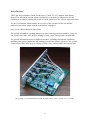
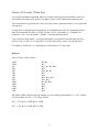
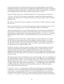
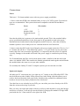
Oakley Sound Systems
Euro and Frac Rack Series
Classic VCA issue 1
Discrete Core Voltage Controlled Amplifier
Builder's Guide
V1.6.1
Tony Allgood
Oakley Sound Systems
CARLISLE
United Kingdom
Introduction
This is the Project Builder's Guide for the issue 1 Classic VCA 3U module from Oakley
Sound. This document contains a basic introduction to the board, a full parts list for the
components needed to populate the board or boards, and a list of the various interconnections.
For the User Manual, which contains an overview of the operation of the unit and the
calibration procedure, please visit the main project webpage at:
http://www.oakleysound.com/vinvca.htm
For general information regarding where to get parts and suggested part numbers please see
our useful Parts Guide at the project webpage or http://www.oakleysound.com/parts.pdf.
For general information on how to build our modules, including circuit board population,
mounting front panel components and making up board interconnects please see our generic
Construction Guide at the project webpage or http://www.oakleysound.com/construct.pdf.
The prototype issue 0 PCB behind a 10HP Scheaffer panel. Issue 1 boards are very similar.
2
Power Supplies
This module is designed to run from plus and minus 12V or 15V supplies. These should be
adequately regulated. The current consumption is about 20 mA per rail. Power is routed onto
the PCB by either:
1. A four way 0.156” MTA or Molex type connector. This the standard Oakley power supply
that is also suitable for MOTM and Fractional rack systems. The four pins are positive rail,
ground, panel, negative rail. The panel connection allows you to connect the metal front panel
to the power supply’s ground without it sharing the modules’ ground line. This panel
connection is normally connected to 0V either on the power supply or on the power
distribution board.
2. A 2 x 5 way 0.1” (2.54mm) header for compatibility with Euro format modular systems.
The top pins on the header are connected to the +12V supply. The module's electronics can be
damaged if the connector is attached incorrectly.
The Classic VCA issue 1 PCB
This is one of our smaller format PCBs. We are expecting most builders to be using the
smaller 3U Euro/Frac sized panel with this module. The pots are specified as Alpha/ALPS
16mm types. The pot spacing on this module is 21mm (0.827”) instead of our usual 41.3mm
(1.625”).
The size of the board is 102mm high by 79mm deep. The board is fitted to the front panel by
either the pots alone, or additionally with two of our small pot brackets.
The input and output sockets are wired to the board via an eight way 0.1” Molex or MTA
interconnect. This makes removing the board from the panel very easy. It also offers the
possibility of connection to a socket board like our VCO and other modules. However, at this
moment in time we have no plans to release a socket board for this particular module.
3
Buying The Components
For general information regarding where to get parts and suggested part numbers please see
our useful Parts Guide at the project webpage or http://www.oakleysound.com/parts.pdf.
Some specific information for parts used in this module:
The single multiturn 100K trimmer is the one that has the adjustment on the top of the box.
Spectrol and Bourns make these. Some types are 20 turns, while others are 25 turns. Either
will do. They should have three pins that are in a line at 0.1” pitch. I generally use the Bourns
3296 series.
The three trimmers are standard sealed carbon units. These are adjusted from the top and, as
such, are called horizontally mounted types. Piher and other companies make suitable types.
Lead spacing is 0.2” for the track ends, and the wiper is 0.4” away. Rapid, Farnell and RS sell
these parts at reasonable cost. You can use the more expensive cermet types if you wish, but
stability is not critical for this application.
The PNP/NPN array is the THAT340 from THAT Corp in the US. This is normally available
from Farnell and other larger distributors. The PNP array is the Analog Devices' SSM2220
and is now obsolete although there is some talk about revitalising it. In the meantime the best
place to get them is Bridechamber in the US or Banzai in Europe.
U3 can be replaced with an OPA134. This is a very high performance part, but I didn't actually
detect any significant advantage in using it.
Input and output sockets are not board mounted. You can choose whichever type of sockets
you wish. If you are mounting this module in a Frac or Euro sized format then you will need
to chose a decent 3.5mm socket to use. Normalised sockets are not required in this module.
However, note that many sockets often have NC lugs as standard. In this case, you can simply
buy them but leave the NC lugs unused. I will say now that I prefer to use insulated sockets,
ie. plastic ones. This stops the module ground being connected to the chassis earth and in
theory prevents earth loops and audible hums. However, a great many of the new Euro
modulars makers are using metal sockets and no one has yet complained of any problems.
This module is entirely suitable for the fitting of 4mm banana sockets. I'd be tempted to
recommend these but for the fact that most Euro systems are exclusively 3.5mm sockets.
This module uses an eight way 0.1” header, SKT, to connect the sockets' leads to the PCB. I
have specified Molex KK connectors, but you could also use Amp's MTA system instead.
Both require a special, and the in the MTA case, an expensive, tool to make up the connector
ends. The MTA is an insulation displacement system where the wires are forced into the
housing by the special tool. The Molex KK system is based on individual crimped contacts
that are inserted into the housing once crimped.
Alternatively with the Molex system you can simply solder your wires into the little metal
contacts before pushing them into the eight way housing. If I were making a lot of Classic
4
VCA modules I would use MTA – but if you are building just the one, go for Molex KK types
and purchase a cheap crimper or solder the wires into the little crimps.
The other option is to not fit the SKT header at all. This way you can solder your connecting
wires directly into the PCB. There is nothing wrong with doing it this way – indeed, it could
be said that this is more reliable. However, remember that the solder pads are quite small and
could be damaged if overheated when soldering or desoldering.
5
Classic VCA issue 1 Parts List
For general information regarding where to get parts and suggested part numbers please see
our useful Parts Guide at the project web page or http://www.oakleysound.com/parts.pdf.
The components are grouped into values, the order of the component names is of no particular
consequence.
A quick note on European part descriptions. R is shorthand for ohm. K is shorthand for kiloohm. R is shorthand for ohm. So 22R is 22 ohm, 1K5 is 1,500 ohms or 1.5 kilohms. For
capacitors: 1uF = one microfarad = 1000nF = one thousand nanofarad.
To prevent loss of the small ‘.’ as the decimal point, a convention of inserting the unit in its
place is used. eg. 4R7 is a 4.7 ohm, 4K7 is a 4700 ohm resistor, 6n8 is a 6.8 nF capacitor.
For Alpha or ALPS pots: A = logarithmic or audio taper, B = Linear taper
Resistors
All 5% carbon 1/4W or better.
220R
470R
1K
3K3
4K7
18K
33K
47K
62K
100K
180K
470K
680K
1M5
R9, R4
R17
R11, R7, R5, R24
R23
R10, R6, R1
R27
R18
R21, R14, R16
R13, R12
R3, R2, R20
R19
R25
R8
R26
The values of R15 and R22 depend whether you are building your module for +/-15V (Oakley
5U & Frac Rack) or for +/-12V (Euro format).
For +/-15V, R15 is 150K, R22 is 180K
For +/-12V, R15 is 120K, R22 is 150K
6
Capacitors
Components marked with a asterisk see Circuit Description section for alternative values.
33pF low-K ceramic
100pF low-K ceramic
100nF axial multilayer ceramic
470nF, 63V polyester
2.2uF, 25V electrolytic
C3*, C5*
C2*, C4*
C6, C7, C8, C9
C1
C10, C11
Discrete Semiconductors
1N4148 signal diode
BC550 NPN transistor
BC560 PNP transistor
D1, D2, D3, D4, D5, D6, D7, D8, D9, D10
Q5, Q10, Q11
Q6, Q7, Q8, Q9
Integrated Circuits
TL071 single op-amp
THAT340P NPN/PNP array
SSM2220 PNP array
U3
U2
U1
Trimmers
100K multiturn trimmer
100K horizontal trimmer
10K horizontal trimmer
OFFSET
EXP, LIN
NULL
Potentiometers
50K logarithmic Alpha 16mm pot
50K linear Alpha 16mm pot
DC_INPUT, AC_INPUT
GAIN, EXPO_CV, LIN_CV
Oakley small pot brackets
Two off
Note that when fitting the three pots without pot brackets a shim washer should be fitted
between the pot and the inside of the front panel. You can use the washer provided with the
pot for this purpose or get another one of similar size so that you can use the provided washer
on the outside like you would normally.
7
Wire link
Fit a small hoop of uninsulated wire (eg. from a resistor lead clipping) into the two holes of
LINK. This joins the two ground pins of the 4-way 0.156” header.
Miscellaneous
0.156" MTA 4-way header
2x5 0.1” header
PWR – Fit for Frac/Oakley systems only
PSU – Fit for Euro systems only
0.1” 8-way Molex or MTA header SOCKETS – board mounted
0.1” 8-way Molex or MTA housing SOCKETS – wire harness
Leaded ferrite beads
L1, L2
Knobs to fit 6mm shafts
3.5 sockets
DIL14 pin IC sockets
DIL 8 pin IC sockets
Five off
Five off
One off
Two off
Hook up wire (26awg) in several different colours
Note: If fitting a boxed header for the Euro power supply then please ensure that the notch in
the box header faces outward. That is it should face towards the back of the modular and
away from the front plate of the module.
8
Circuit description
The Oakley Classic VCA is based around the old ARP module 4019. This module was built on
an incredibly tightly cramped circuit board which was then securely potted, with a very hard
epoxy compound, into a small plastic box. The various interconnections were made to some
thin gold plated legs that stuck out from the hard epoxy on the underside. It is almost
impossible to remove the circuitry from its hard plastic shell and all encompassing resin. I
suppose this was mostly down to Alan Pearlman's previous history in making op-amps for the
aerospace industry – enclosing circuits like this would make them less likely to drift with
temperature and not be affected by surrounding humidity. However, one might also think that
they did it to keep out the prying eyes of their competitors.
Later versions of the 4019 used soft and rubbery silicone to pot the circuitry into its shell with
only a thin layer of epoxy on the underside to seal it all in. These types are easier to repair
since it is now possible, with some care, to remove the delicate circuitry from its shell and
potting compound. Various folk have since reverse engineered this circuit and it can be found
in various places on the internet.
Interestingly the very first 2600 synthesisers had the 4010 VCA module installed. I have not
been able to find out much about this particular module suffice to say that it was physically
smaller and probably less reliable than the later version. The fact that it was smaller surely
meant that it contained less circuitry compared to its successor.
Purchasers of the Oakley Classic VCA PCB will be able to obtain a copy of the schematic. On
the schematic it should be noted that the power supplies are shown as +/-15V, but these can
also represent +/-12V. The circuit will run from either supply although there is one small
resistor value different depending on which supply you are using. The circuit itself looks pretty
unusual but it can be split up into two smaller parts to make understanding it a bit easier.
The first part of the schematic we will look at is the CV processing. This takes the two CV
inputs, processes them and turns them into a small current that will control the gain of the
VCA core. You can find the CV processing circuit on the left hand side of the schematic.
The linear and exponential inputs are processed separately. The top left hand circuit, based
around Q9 and Q10, deals with the exponential input. The CV input is controlled by its own
level pot, EXPO_CV, and is configured as the usual voltage divider. As the wiper moves up
and down a proportion of the input voltage is fed into R21.
Q9 and Q10 form a standard ARP style exponential convertor. The precise actions of this go
beyond this simple document, but it can be shown that for every 18mV increase in Q9’s base
voltage we double the current going through Q10. Q10 draws this current from the VCA core
of which we will discuss later.
EXP is a trimmer, a set and forget type of device, and allows adjustment of the maximum gain
of the VCA from the exponential CV input.
The linear input is also controlled by a pot, this time LIN_CV, and it is passed via R14 to a
summing node at the junction of R15, R16 and R17. This node is held at around 0V by the
9
actions of Q8 and D3. Q8 and Q7 form an old style DC coupled amplifier. Q8 does all the
amplification while Q7 provides some level shifting and output buffering. Negative feedback is
provided by the trimmer LIN and R16. LIN therefore provides some adjustment over the gain
of the amplifier block and thus sets the sensitivity of the linear CV input.
Note the GAIN pot, this is one of the front panel pots. The wiper of this pot can go from
+15V (or +12V) to 0V. This voltage is turned into a current by R15 and injected into the
summing node. Thus both the CV input and GAIN pot control the output voltage of the little
amplifier circuit.
R27 and Q11 then turn this output voltage into a current which, in tandem with Q10, controls
the VCA core.
Now let us look at the VCA core itself. This comprises of the two transistor arrays, U1 and
U2, and the surrounding circuitry. It can be found in the middle of the schematic.
The basic topology of the VCA core is fairly standard. Its a transconductance amplifier built
almost entirely from discrete transistors. The unusual thing about it, at least as far as most
synth designs go, its upside down. The input transistors, U2 pins 8, 9, 10 & 5, 6, 7, are PNPs.
Most designs use NPNs. However, lets put that aside and see if we can work out how it
works.
The signal enters the VCA via either, or both, of the two socket connections, AC_IN and
DC_IN. They are both identical except for the addition of a 470nF capacitor, C1, on the
AC_IN. This capacitor acts to block steady state voltages (DC) and very low frequencies. In
other words it acts like a high pass filter. The cut-off varies a little with the position of the
AC_INPUT pot, but it is approximately 10Hz.
R3 and R2 carry their respective signals to attenuate (reduce) and sum together at R4. The
voltage across R4 being a tiny fraction, approximately 0.2%, of what it was at the socket
inputs. Both inputs are applied to the right hand input PNP transistor. The other input
transistor, the left hand one, is simply connected to a very low voltage that is generated by the
OFFSET trimmer, R8 and R9. We use this trimmer to manually balance the left and right sides
of the VCA core.
The voltage supply to the transconductance stage is fixed by diodes. The series combination of
D7, D9, D10 provide a steady +1.8V for the top of the circuit. While the series combination of
D6 and D8 provide a steady -1.2V for the bottom of the circuit. When current passes through
a diode it tends to have 0.6V across it. +1.8V and -1.2V may appear to be a very small range
of supply voltage for a module that can handle nearly +/- 10V input signals. But remember the
actual input transistors will only be working with that tiny fraction of the input signal to
prevent them from distorting the signal.
U1 (pins 6, 7, 8 & 1, 2, 3) and Q6 make a special circuit which engineers call the Wilson
current mirror. It is a clever little design and is found in many different circuits. The Wilson
current mirror is a programmable current source. Its programmed by the CV processing
circuitry which we discussed earlier. Any current drawn out from the collector of transistor
U1 (pins 6, 7, 8) by the CV processing circuit is then replicated by the mirror and provided to
10
the circuitry connected to the collector of Q6. Thus the input transistors of the VCA core are
supplied with a current that is directly controlled by the CV signals.
The two NPN transistors from U2 (pins 12, 13, 14 & 1, 2, 3), along with Q5 and D5 act as
another current mirror. The current drawn down by each NPN transistor in U2 will be the
same due to the actions of the mirror. However, when an input signal is applied to one of the
input PNP transistors this equality of current is challenged. But the current mirror will do its
very best to maintain equilibrium so any 'excess' current is taken away by the op-amp U3. This
current is the VCA core's output signal and it should be reiterated that it is a current not a
voltage. Indeed, if you were to slap your 'scope probe on this point you would see very little
happening. The voltage remains, due to the actions of the op-amp, firmly stuck at around zero
volts.
It should be noted at this point that the current output of the VCA core, the transconductance
amplifier, is directly proportional to the current being supplied by Q6. After all this is where
the input transistors get their current from in the first place. Remember that no significant
current is actually taken from the input signal via the base of the PNP transistors. So if the
output current is dependant on the current provided by Q6, then controlling this current allows
us to control the gain of the whole transconductance amplifier. This is why our CV processing
circuit is tied to the top current mirror of the core. It has direct control over the gain and this
is what makes it a VCA.
The op-amp is configured as an inverting transimpedance amplifier, which is a 'current in,
voltage out' device and essentially the opposite of a transconductance amplifier. A
transconductance amplifier followed by a transimpedance amplifier make an amplifier, ie.
'voltage in, voltage out'. The 'gain' of the transimpedance amplifier is primarily set by R12. The
output of the op-amp passes via R11 to the output socket of the module.
A standard transimpedance amplifier is just an op-amp and a resistor. This one looks more
complex – its has four additional capacitors, two extra resistors and also a trimmer. C2, C5
and C4 all act to ensure stability of the circuit. No real life circuit is perfect, and without
getting into the maths of it, unwanted characteristics of the components and board layout act
to sometimes make the circuit unhappy. Typically this will mean it will oscillate when it
shouldn't, or more commonly it will nearly oscillate when it shouldn't. The latter is called
ringing and it is a resonance effect. In other words the circuit has a tendency to bounce around
at a particular frequency when excited by an input signal.
When using a TL071 for U3 and not fitting any of the capacitors, the VCA would ring
horribly at a very high frequency. This is way above human hearing but any ringing is not a
good thing. Using all the values that ARP used made the circuit very stable, ie. no ringing, but
it reduced the overall frequency response so that it had a negative impact on the audio
bandwidth of the VCA. This raised an interesting question regarding the frequency response of
a real ARP2019 since the drop in high frequency audio is audible. If you want to stick to the
original values make C2 and C4 both 100pF. C5 can be 33pF. It is these values that are on the
schematic.
If you would like the VCA to have a full bandwidth then reduce the values of C2 and C4 and
omit C3 and C5 entirely. I have used 18pF for C2 and C4 with excellent results. If you have
not fitted C3 you can then omit the NULL trimmer and R10.
11
R13 provides the op-amp with equal resistances on its inputs. The inverting input 'sees' only
R12 since the resistance of the transimpedance amplifier is so high one can normally ignore it.
However, the TL071 is very forgiving about imbalances of resistance on its inputs (it has very
low bias currents because it is a FET amplifier) so R13 would normally be unnecessary. I have
left it in to be faithful to the original ARP module. It also allows us to use the NULL trimmer.
The NULL trimmer is designed to pass back a proportion of the input signal to C3. C3 acts in
conjunction with R12 to make a high pass filter. This means that only the very highest audio
frequencies are passed into the non-inverting input of the op-amp. Since they expected the
transconductance core to leak a little at high frequencies, one could then, in theory, cancel
these leaks out by subtracting the core output with a high pass filtered version of the input. It
seems it didn't work since the ARP say in their service notes, with regards to the trimmer, 'no
adjustment necessary'. However, for the sake of accuracy the circuit has been replicated here
in full. I didn't find it particularly helpful reducing high frequency breakthrough either, but
there may be some scope for experimenting here.
Power is supplied via the usual four way MTA or Molex connector and 10 way Euro style
power connector. As is the custom for Oakley modules, I have used ferrite beads to act as
high frequency filters on the power lines. Decoupling at the point of entry is provided by C10
and C18 for the positive rail, and C11 and C9 for the negative rail. Additional decoupling is
also provided elsewhere on the board by the other capacitors shown at the top of the
schematic. All these capacitors keep the power supply clean of noise, and provide a reservoir
for the little bursts of current that the circuit takes in normal operation.
12
The idea behind the Oakley Classic VCA module
This is very first version of the Oakley Classic VCA fitted to a real ARP2600C. This one off
clone was built to replace a dead 'all epoxy' 4019 VCA module which in itself had replaced an
older 4010 VCA module. Note the pin out placement to accommodate the smaller 4010
module.
I later compared this 2600C to an early 2600P fitted with a standard 4019 module and the
differences were negligible in all but the increased frequency response of the clone.
The large red polypropylene capacitor fitted to the underside of the main circuit board is a
modification done to provide DC blocking to the VCA on one of its inputs. The ARP2600 is
predominantly DC coupled, but this tends to unbalance the VCA since many of the VCO
waveforms are unipolar, ie. all positive. This positive bias of the VCA input leads to thumping
at fast attack and release settings. The capacitor removes the bias and allows for fast thump
free sounds. The action of the red capacitor is much the same as the INPUT (AC) on this
module.
13
Connections
Power
This issue 1 3U format module comes with two power supply possibilities.
1. Power connection PWR is the standard Oakley 4-way 0.156” MTA socket. Friction lock
types are recommended. This system is backward compatible with MOTM and Blacet
systems.
Power
Pin number
+15V
Module GND
Earth/panel metal
-15V
1
2
3
4
Note that the third pin is separate to the main module ground. This is the standard Oakley
power specification and allows for the front panel to be grounded to earth at the power
distribution board rather than locally through the module. However, other than in Oakley
modular systems it is not widely used. See comment about the wire link below.
2. Power connection PSU is the 10 pin Doepfer style power supply connection. This is a 2 x 5
0.1” header and will fit 0.1” Flat ribbon IDC sockets. +12V goes to the top two pins of the
header, that is the ones nearest the legend PSU. It is imperative that the power be supplied
correctly. Damage to the module will result if the power supply is connected up the wrong
way.
For Fractional Rack and Euro sized systems please solder a small wire link into the board
where it is labelled LINK. This connects the module ground and earth together and will make
the module behave the same way as your other modules.
For assembly into Oakley 5U and 3U complete systems you can omit the wire link.
Inputs and outputs
All audio and CV connections are via a eight way 0.1” header on the PCB called 'SKT'. This
may be different to other Oakley PCBs you may have built. Doing it like this allows you to
remove the board from the front panel easily, and allows the potential for additional socket
boards to be used in any future production run of the board.
You don't have to use a header in your PCB, you can solder your wires directly to the PCB
from the various socket lugs if you wish.
How you wire your input and output sockets up will very much depend on your panel design
and choice of sockets. I will only go into the details of wiring up the standard 3U high 10HP
panel with the five 3.5mm sockets to the right of the PCB.
14
For my prototype I used Cliff jack sockets. I used these because they are relatively cheap and
provide insulation between the module panel and the module ground. The module panel will
be grounded or earthed via the rack casing. It is usually a good idea not to allow any local
module ground to come into contact with the chassis at multiple points as this has the
potential to cause ground loops and hums in your audio outputs.
Furthermore, as far as I can see it, most Euro rack systems are wired in such a way as to allow
an additional ground pathway to occur whenever a patch cable is plugged from one module to
another. However, since there has not been a chorus of complaints regarding multiple earth
loops and hum problems, I think we can take it that it is not a major problem. The Oakley
modular system circumvents this whole complicated issue by using a second ground
connection to provide a panel earth on each module. Thus panels and local grounds are
distinct except for at one point near the power supply.
If you have used the little Cliff sockets you will see that they have four connections. One is the
earth lug or ground tag. The second is the signal tag which will be connected to the tip of the
jack plug when it is inserted. The third and fourth tag are the normalised tags, or NC
(normally closed) lugs. The NC lugs are each internally connected to the ground and signal
tags when a jack plug is not inserted. These connections should be automatically broken when
you insert a jack.
Most 3.5mm sockets with metal bushes have only one NC lug, that is these sockets will have
just three connections. Their NC lug will be connected to the signal lug of the socket when no
jack is inserted.
Pushing a jack plug into an unconnected socket and looking carefully at the various contacts
will reveal the actions of the NC lugs.
Fit the five sockets onto the panel so that the all the socket's tags face left as you look at the
rear of the panel, ie. away from the PCB.
In this module we are going to ‘common’ the sockets’ ground lugs. This means that the
sockets’ earth lugs are going to be joined together so we only need one piece of insulated
interconnection wire to ground all the sockets. I normally do this part of the wiring without
the PCB or pots in place on the panel. I use thin uninsulated tinned copper wire, its just stiff
enough so as to retain its shape. Solder a length of this solid core wire right across all the tags
nearest to the panel. These are the earth tag, and its corresponding NC tag if you have them,
on all the sockets. Trim off any excess wire that sticks out on either end. This single wire will
eventually be connected to the printed circuit board via pin 3 of the SKT header.
If your chosen sockets do not have an earth NC lug, this is fine. Simply make sure that all your
socket grounds are connected together.
Fit the Classic VCA PCB against the front panel if you haven't done so already. For my
prototype I used Molex KK headers and housings to connect my module's sockets to the
circuit board.
Use multistrand hook up wire to connect each socket lug to the relevant pin on the header.
Keep your wires short but not too short and you can use as many different colour wires as you
15
can – although I tend to use one colour because I'm a minimalist. There is absolutely no need
to use screened cable for such short runs.
The connections to the signal and NC lugs of the sockets that go directly to the PCB are
summarised in the table below. They are given in the order in which I would recommend that
they be soldered.
Socket Name
SKT Pin number
Lug Type
INPUT (AC)
INPUT (AC)
INPUT (DC)
INPUT (DC)
OUTPUT
LIN CV
LIN CV
EXPO CV
EXPO CV
1
5
2
5
4
6
7
8
7
Signal
NC
Signal
NC
Signal
Signal
NC
Signal
NC
With the NC lugs you can simply connect the NC lugs of each pair of sockets together and
take just one wire back to the header on the PCB.
Finally Pin 3 is connected to the single uninsulated wire that joins the socket ground tags.
Once that is done, your module is ready for testing and calibration.
16
Testing, testing, 1, 2, 3...
Apply power to the unit making sure you are applying the power correctly. Check that no
device is running hot. Any sign of smoke or strange smells turn off the power immediately and
recheck the polarity of the power supply, and the direction of the ICs in their sockets.
Assuming everything is OK so far, it is time to apply an audio input. Use a signal like a
triangle output from a VCO. Middle A, 440Hz is a good note to use. Turn down all the pots
to their minimum setting and insert your triangle wave signal into INPUT (AC). Listen to the
output signal from the VCA module. For the moment you should hear nothing.
Turn up the INPUT (AC) pot to full. Again, you shouldn't hear anything, but maybe you will
hear a little triangle wave bleedthrough. Now slowly turn up the GAIN pot. If all is well this
should behave like a volume control, increasing the level of the triangle wave as it is turned
up.
Ensure that altering the INPUT (DC) pot should have no effect on the sound, but that INPUT
(AC) behaves also like a volume control. It should seem that both INPUT (AC) and GAIN do
the same thing. They do not of course, since INPUT (AC) is altering the signal level going
into the VCA circuit, and GAIN is adjusting the amplification within the VCA's core.
Swap the input signal over to the INPUT (DC) input. It should be quiet again. Turning up the
INPUT (DC) pot should bring back the signal.
There is a very good chance your circuit is working correctly if you have got this far with no
problems. However, we still need to check a few other things and you'll need another signal
source to do this. Connect a LFO or VC-LFO to the LIN CV input. Use a sine or triangle
wave signal at a lowish frequency, say 1Hz or so.
Turn the GAIN down to about 50% and the LIN CV up. Listen to the resultant sound. It
should be the triangle wave you can hear again, but it will plusate evenly up and down with
LFO signal. You should hear it go up and down in volume once for every cycle of the LFO.
Now remove the LFO signal from the LIN CV socket and connect it to the EXPO CV socket.
Turn up the EXPO CV pot and you should hear the same sort of pulsating sound. However, it
should be slightly different, spending more time loud than quiet..
If all is well, then you have a working VCA module.
17
Final Comments
If you have any problems with the module, an excellent source of support is the Oakley Sound
Forum at Muffwiggler.com. Paul Darlow and I are on this group, as well as many other users
and builders of Oakley modules.
If you can't get your project to work, then Oakley Sound Systems are able to offer a 'get you
working' service. If you wish to take up this service please e-mail me, Tony Allgood, at my
contact e-mail address found on the website. I can service either fully populated PCBs or
whole modules. You will be charged for all postage costs, any parts used and my time at
25GBP per hour. Most faults can be found and fixed within one hour, and I normally return
modules within a week. The minimum charge is 25GBP plus return postage costs.
If you have a comment about this builder's guide, or have a found a mistake in it, then please
do let me know. But please do not contact me or Paul Darlow directly with questions about
sourcing components or general fault finding. Honestly, we would love to help but we do not
have the time to help everyone individually by e-mail.
Last but not least, can I say a big thank you to all of you who helped and inspired me. Thanks
especially to all those nice people on the Synth-diy and Analogue Heaven mailing lists and at
Muffwiggler.com.
Tony Allgood at Oakley Sound
Cumbria, UK
© May 2009 - updated June 2013
No part of this document may be copied by whatever means without my permission.
18