1
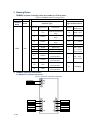
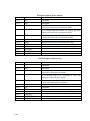
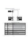
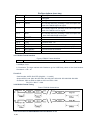
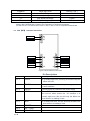
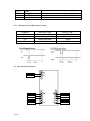
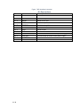
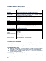
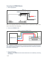
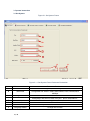
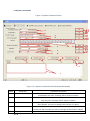
RDM Tag Module RDM880 13.56MHz RFID Reader/Writer ISO\IEC 14443A ISO\IEC 14443B ISO\IEC 15693 PRODUCT REFERENCE GUIDE RDM880 April 2007 Shenzhen RDM Tag Master Co., Ltd. | www.datarfid.com 1 / 28 Document Title RDM880 Reference Guide Version 1.0 April 9, 2007 4F, #25Bld, NO.5, Kezhi West Road, Hi-Tech Park, NanShan ShenZhen, China Tel: +86-755-86329278 Fax: +86-755-26639115 http://www.datarfid.com RDM880 Reference Guide. 4F, #25Bld, NO.5, Kezhi West Road, Hi-Tech Park, NanShan ShenZhen, China Tel: +86-755-86329278 Fax: +86-755-26639115 http://www.datarfid.com 2 / 28 Contents Product Overview 1. General Description……………………………………………………........................................ 4 RDM880 Module Introduction 1. RDM880 Mechanical Specification………………………………………….………... 5 2. Naming Rules……………………………………………………………….……….…..6 3. RDM880 Interface Instruction………………………………………………….……….6 3.1 RS232/TTL Interface Instruction……………………………………………….…..6 3.2 RS232/RS485 Interface Instruction………………………………………..………8 3.2.1 TS232 Format Interface………………………………………………………9 3.2.2 RS232 Format Timing…………………………………………………………9 3.2.3 Connection of RS232/RS485 Interface Module To PC……………………9 3.3 ABA (AT) Interface Instruction……………………………………………………...10 3.3.1ABA TRACK2 Format Interface ……………………………………..…….….11 3.3.2ABA TRACK2 Format Timing……………………………………………...…..11 3.4 WG(WT) Interface Instruction……………………………………………….………12 3.4.1 Wiegand Format 26bit Output Timing…………………………………….….13 3.5 SPI Interface Instruction……………………………………………….…………….13 4. RDM880 Interface Specification………………………………………………………...15 5. RDM880 Typical Applications…………………………………………………………...15 6. RDM880 Operating Mode………………………………………………………………..15 7. RDM880 Adjacent Module Identification……………………………………………….15 Connecting the RDM880 Module 1. 2. 3. 4. Power Supply Options……..………………………………………………………..…...16 Connection of RDM880 To PC……………………………………………………...…..16 Antenna Connections……………………………………………………………...…….16 LED and Buzzer Connections………………………………………………………..…17 RDM880 DEMO Software 1. DEMO Software…………………………………………………………………………..17 2. DEMO Software Flow Chart………………………………………………....................18 3. Operate Instruction……………………………………………………………………….19 3.1 Set System……………………………………………………………………………19 3.2 System Command…………………………………………………………...……….20 3.3 ISO 14443 Type-A Commands……………………………………………………..22 3.4 ISO 14443 Type-B Commands……………………………………………………..24 3.3 ISO 15693 Commands………………………………………………......................25 3 / 28 Product Overview 1. General Description The RDM880L module is a Mifare® ISO14443 A read/write device with a typical operating distance of 30-80mm. The reading range of the module is depending on the antenna and TAG. The RDM880L combines all basic functions to access the ISO14443A Card. Including Mifare® Smart Card, Mifare PRO etc. Its versatility allows a flexible and efficient application in different configurations and system devices. Because of the small size the module can be integrated easily into existing data collection applications such as portable terminals, ticketing, machines vending or access control. The 13.56MHz RDM880L OEM read/write module is a very compact device designed for fast integration into portable or stationary readers. The OEM reader module was designed for simple integration. The serial TTL-interface can be directly connected to microprocessors and easily converted to the RS232/RS485/RS422 serial interface device. The protocol can be tested using any terminal. 4 / 28 RDM880 Module Introduction 1. RDM880 Mechanical Specification Size: 39*19*9 mm Antenna: External Signal:2Led& 1Beep(TTL) Figure 1 Top View Of RDM880 Dimensions in mm Figure 2 Side View Of RDM880 5 / 28 2. Naming Rules RDM880 module’s naming rules are made up of four parts. Figure 3 RDM880 Module’s naming rules Part 1 Part 2 Company Name Code RDM 880 Part 3 - Part 4 - Interface Type Type Of Smart Card Symbol Signification Description Symbol Type of smart card T TTL Read & Write/Read Only A S50、S70 S RS232 Read & Write/Read Only B ISO14443B R RS485 Read & Write/Read Only C TI、I Code2 I SPI Read & Write D Desfire W WG26 Read Only G WG34 Read Only E A ABA Read Only S50、S70、 TI、I Code2、 ISO14443B ST RS232 Read Only (Configurable) F S50、S70、 ISO14443B U Ultralight - - RT RS485 Read Only (Configurable) WT WG Read Only (Configurable) ABA Read Only (Configurable) AT 3. RDM880 Interface Instruction 3.1 RS232/TTL Interface Instruction Figure 4 RS232/TTL interface instruction ANTENNA + ANTENNA - 6 / 28 BUZ +5V(DC) LEDR GND LEDG TXD(R+) NC RXD(R-) NC RESET Pin Descriptions (Read & Write) Description Pin J1-1 Name NC J1-2 J1-3 NC LEDG Obligate J1-4 LEDR It is usually high level which can control the LED when the low level is connected to GND. J1-5 BUZ J2-1 J2-2 J2-3 J2-4 J2-5 J3-1 J3-2 RESET RXD TXD GND +5V(DC) ANTENNA ANTENNA + It is usually low level, this pin can control the buzzer when the high level is connected to GND. Reset Connects with R1OUT(a 232PWL drive chip) Connects with T1IN a 232PWL drive chip) Connects with the cathode of the power supply Connects with the anode of the power supply Connects with the antenna Connects with the antenna Obligate It is usually low level, this pin can control the LED when the low level is connected to GND. Pin Descriptions(Read Only) Pin J1-1 Name NC Description J1-2 J1-3 NC LEDG Obligate J1-4 LEDR It is usually high level, punching a card will discontinue the low level signal. J1-5 BUZ It is usually low level, punching a card will expand the time of the 88US high level signal. J2-1 J2-2 J2-3 J2-4 J2-5 J3-1 J3-2 RESET NC TXD GND +5V(DC) ANTENNA ANTENNA + Reset 7 / 28 Obligate It is usually low level, punching a card will discontinue the high level signal. Obligate Connects with T1IN a 232PWL drive chip) Connects with the cathode of the power supply Connects with the anode of the power supply Connects with the antenna Connects with the antenna 3.2 RS232/RS485 Interface Instruction Figure 5 RS232/RS485 interface instruction ANTENNA + ANTENNA - BUZ +5V(DC) LEDR GND LEDG TXD(R+) NC RXD(R-) NC RESET Pin Descriptions (Read & Write) Description Pin J1-1 Name NC J1-2 J1-3 NC LEDG Obligate J1-4 LEDR It is usually high level which can control the LED when the low level is connected to GND. J1-5 BUZ J2-1 J2-2 J2-3 J2-4 J2-5 J3-1 J3-2 RESET RXD TXD GND +5V(DC) ANTENNA ANTENNA + It is usually low level, this pin can control the buzzer when the high level is connected to GND Reset Receive Data(R+) Transmit Data(R-) Connects with the cathode of the power supply Connects with the anode of the power supply Connects with the antenna Connects with the antenna 8 / 28 Obligate It is usually low level, this pin can control the LED when the low level is connected to GND. Pin Descriptions (Read Only) Description Pin J1-1 Name NC J1-2 J1-3 NC LEDG Obligate J1-4 LEDR It is usually high level, punching a card will expand the time of the 88US low level signal. J1-5 BUZ It is usually low level, punching a card will expand the time of the 88US high level signal. J2-1 J2-2 J2-3 J2-4 J2-5 J3-1 J3-2 RESET RXD TXD GND +5V(DC) ANTENNA ANTENNA + Reset Obligate It is usually low level, punching a card will expand the time of the 88US high level signal. Receive Data(R+) Transmit Data(R-) Connects with the cathode of the power supply Connects with the anode of the power supply Connects with the antenna Connects with the antenna 3.2.1 RS232 Format Interface Figure 6 RS232 Format Interface 02 10 ASCII Data Characters Checksum 03 a. 9600bps, N,8,1. b. Checksum: The byte marked with Checksum go for XOR Parity check of the Card Number. Checksum = CR + LF. EXAMPLE: Card Number: 62 E3 08 6C ED (High bit ---- Low bit) Output ASCII Code: 02H 36H 32H 45H 33H 30H 38 H 36H 43H 45H 44H 30H 28H 03H Checksum: 62H xor E3H xor 08H xor 6CH xor EDH = 08H SO: CR = 30h LF = 38H 3.2.2 RS232 Format Timing Figure 7 RS232 format timing 3.2.3 Connection Of RS232/RS485 Interface Module To PC 9 / 28 Figure 8 connection of RS232/RS485 interface RDM880 TO PC 3.3 ABA(AT) Interface Instruction Figure 9 ABA interface instruction ANTENNA + ANTENNA - BUZ +5V(DC) LEDR GND ABA DATA NC(TXD) ABA CLOCK NC(RXD) HOLD RESET Pin Descriptions Description Pin J1-1 Name HOLD J1-2 J1-3 J1-4 ABA CLOCK ABA DATA LEDR ABA CLOCK J1-5 BUZ The BUZ interface connects with the cathode of the buzzer, the beep can be controlled by user port (which needs added drive), It is usually low level, punching a card will expand the time of 200ms high level. J2-1 RESET Reset 10 / 28 It is usually high level, the pin will keep the low level of 80ms. ABA DATA It is usually high level, punching a card will expand the time of 300ms low level. J2-2 J2-3 J2-4 J2-5 J3-1 J3-2 NC(RXD) NC(TXD) GND +5V(DC) ANTENNA ANTENNA + Obligate Obligate Connects with the cathode of the power supply Connects with the anode of the power supply Connects with the antenna Connects with the antenna 3.3.1 ABA TRACK2 Format Interface Structure of ABA TRACK2 data message is : 0000000000 11010 1248P 1248P 1248P 1248P 1248P 1248P 1248P 1248P 1248P 1248P LRC 00000 Leading Zero is 0 of 10 digits Start Char is HEX “B” (11010,Low bit first,1248P, P is Bit Odd Parity) Card Number is 0000000000~9999999999(10 digits) with most significant digit first End Char is HEX “F” (11111, Low bit first,1248P, P is Bit Odd Parity) Longitudinal Redundancy Check(LRC) is Even Parity check(excluding the parity bit) Trailing Zero is 0 of 5 digits Data transferred LSB first Example: B0 B1 B2 B3 P Start Char.. 1 1 0 1 0 Card Data 1 0 0 0 0 0 1 0 0 0 1 1 0 0 1 End Char. 1 1 1 1 1 LRC 0 0 1 0 0 LRC= START ⊕ DATA0 ⊕ …… Note: ⊕ is XOR ⊕ DATAN ⊕ END 3.3.2 ABA TRACK2 Format Timing Figure 10 ABA TRACK2 Format Timing CP CP SS SS SS DATA DATA SS CLK CLK THD TCH THD TCH TSD TSD SS SS TCL 11 / 28 11111 0 0 0 0 0 0 TCL 0 0 1 1 1 1 1 0 0 0 0 0 0 0 0 0 0 0 0 1 1 1 1 1 0 0 0 0 0 0 SYMBOL THD TSD TCL TCH DESCRIPTION Start Delay Stop Delay CLK pulse low width CLK pulse high width VALUE( Typ. ) 0.5ms 0.5ms 0.5ms 0.5ms A card containing the hexadecimal data (0411115EA6) will be converted to denary and sent as denary 00017466220198 (14 digits).The calculation is performed as follows: (6*160+10*161+14*162+5*163+1*164+1*165+1*166+1*167+4*168)=00017466220198 3.4 WG(WT) Interface Instruction ANTENNA + ANTENNA - BUZ +5V(DC) LEDR GND DATA1 NC(TXD) DATA0 NC(RXD) HOLD RESET Figure 5 WG interface instruction Pin Descriptions Description Pin J1-1 Name HOLD J1-2 DATA0 Connects with the anode of the power supply 1.6MS/120/80US J1-3 J1-4 DATA1 LEDR Connects with the cathode of the power supply J1-5 BUZ J2-1 J2-2 J2-3 RESET NC(RXD) NC(TXD) It is usually low level, this pin will keep the 88ms low level when it is reading a card. Reset Receive Data Transmit Data 12 / 28 It is usually high level, punching a card will keep the 45ms low level. The LEDR interface connects with the cathode of the red led, which control the I/O interface. It is usually high level, this pin will keep the 88ms low level when it is reading a card. J2-4 J2-5 J3-1 J3-2 3.4.1 GND +5V(DC) ANTENNA ANTENNA + Connects with the cathode of the power supply Connects with the anode of the power supply Connects with the antenna Connects with the antenna Wiegand Format 26bit Output Timing SYMBOL THD TSD TDW TIW DESCRIPTION Sending Start Delay Sending Stop Delay Data pulse width Data pulse interval width VALUE( Typ. ) 1.2ms 1ms 160us 880us 3.5 SPI Interface Instruction ANTENNA + ANTENNA - SPISCK MISO GND MOSI NC SPISS NC NC 13 / 28 +5V(DC) RESET Figure 7 SPI interface instruction Pin Descriptions Description Pin J1-1 Name NC J1-2 J1-3 J1-4 SPISS MOSI MISO SPISS of any CPU J1-5 J2-1 J2-2 J2-3 J2-4 J2-5 J3-1 J3-2 SPISCK RESET RXD TXD GND +5V(DC) ANTENNA ANTENNA + SPISCK of any CPU 14 / 28 MOSI of any CPU MISO of any CPU Reset Receive Data Transmit Data Connects with the cathode of the power supply Connects with the anode of the power supply Connects with the antenna Connects with the antenna 4. RDM880 Interface Specification Figure RDM880 Interface Specification Model No. R/W chip Standard Support Card Frequency Baud Rate Power supply Current Static working current Working current Power dissipation Operating range interface Working temperature Storage temperature Size Optional antenna(customized) Relative Provide RDM880 MFRC500,MFRC400,MFRC531,MFRC632 ISO/IEC14443-A;ISO/IEC14443-B; ISO/IEC 15693 MifareOneS50; MifareOneUltralight; MifareOneS70; MifarePro; AT88RF020; 66CL160S; SR176; SRIX4K; I-code2; TI RFID Tag-it HF-I,EM4135,EM4034 13.56MHz 9600-115200bit/s(configurable, default9600) DC5V(5%) <70mA 31mA 67mA 0.3W 30-100mm(reading range depend on antenna and card/tag) TTL electrical level/RS232,RS485,WG,ABA,SPI -10 degree to 70 degree -20 degree to 80 degree 39*19*9 mm(DIP28) 20*40mm 49*55mm 40*71mm 65*90mm 155*166mm(special, required customized) Provide SDK free,DEMO program 5. RDM880 Typical Applications: Many applications can be developed with the RDM RFID module such as PC logon, Internet/intranet access, e-commerce, point of sale, identity confirmation; Access control, Offline Ticketing, Customizing cards, Road pricing etc. in all everywhere a PC or Microprocessor needs to communicate with a contactless transponder. 6. RDM880 Operating Mode Master Slave Operation Mode, under this working style, the reader that is working under the control of the PC or other controllers, communicates with the controller through the port. Active Working Mode, the reader read the card which is in the card-read range, and then output the data from the interface. 7. RDM880 Adjacent Module Identification RDM880 Adjacent Module Identification, adjacent identification is designed for reducing the data redundancy, when using this function, when the reader reads the identical tag repeatedly, it only can upload a set of data( the cards in the card read range at the same time) 15 / 28 Connecting the RDM880 Module 1. Power Supply Options Figure 8 RDM880 powered at J2-5 = DC5V(5%) DC5V GND Note: In the configuration shown above, The Module requires a regulated input voltage in DC5V input to J2-5(an input in this configuration). 2. Connect ion Of RDM880 To PC Figure 9 connection: RDM880 TO PC GND RDM880 Module RXD TXD Note: In addition to the signals connections, the host must supply input voltage. See Figure 8. If the module’s interface is RS232, it’s output format needs to be converted by a chip when the module is connected to pc. 3. Antenna Connections All Models of the RDM880 have two internal antennas that can be enabled by connecting J3-1 and J3-2 . 16 / 28 Figure10 Connecting the Antenna J3-1 J3-2 4. LED and Buzzer Connections Figure11 LED and Buzzer Connections Note: For any interface of RDM880 modules, the LEDR pin is connected to the red LED, and the LEDG pin is connected to a green LED, the BUZ pin is connected to the buzzer. RDM880 Module DEMO Software The use surroundings are different for the RDM880 different interfaces, but the principal for the operation of the demo software is same, following take RS 232 as the samples to explain its operation method. 1. DEMO Software The DEMO software is a low-level tool to show the software developer exactly how a REQUEST is sent to the RDM880 module by a host and the exact RESPONSE from the RDM880 module is provided to the host. Hardware requirement: 1. at least 32M EMS memory 2. at least 2M graphic memory Software requirement: 1. Microsoft Windows 2000/XP/2003 operate system 17 / 28 2. adjusted the desktop resolution ratio to 1024*768 or higher 2. DEMO Software Flow Chart Run the software Input the parameters, click the corresponding button If exit no if open the port yes use dll function yes End 18 / 28 show the related information 3. Operate Instruction 3.1 Set System Figure 3.1 Set System Frame B C F G H Figure 3.1.1 Set System Frame Parameter Declaration Lable Parameter name Parameter Declaration A Port Changeable, controlled by Label G. B Baud Rate Changeable and Select in 9600,19200,38400,57600,115200,Deault 9600bps. C Length of Data Fixed, Default 8bit. D CRC Changeable, and select in Odd, Even and None, Default None。 E Address The address of equipment, Fixed, Default 00H. F Mode Send Selectable. G COM Switch Open or Close the selected COM Port. H Language Switch Change into Chinese. 19 / 28 3.2 System Commands Figure 3.2 System Command Frame A B C D E D1 F G H I J K L1 L Figure 3.2.1 System Command Frame Parameter Declaration Label Parameter Parameter Declaration A Set Address of Reader Input the new address of Reader in Label A, and click Label A1 to set the new address, the return message will be shown in Label L. B Set Baud rate Select a new baud rate in Label B, and click Label B1 to set the new baud rate, the return message will be shown in Label L. C Set SN of Reader Input the new SN of Reader in Label C, and click Label C1 to set the new SN of Reader, the return message will be shown in Label L. D Set User Information Input the new User information in Label D and D1, and click Label D2 to set the new SN of Reader, the return message will be shown in Label L. E Read User Information Input the area and the length of data of user information you wanted, click 20 / 28 Label E1 and the objective user information will be shown in Label L. F Led Mode Input the periodicity and the time of the Led in Label F, click F1 to set the new periodicity and time of the Led, the return message will be shown in Label L. G Buzzer Mode Input the periodicity and the time of buzzer in Label G, click G1 to set the new periodicity and time of the buzzer, the return message will be shown in Label L. H Read Version of Reader Click here and the current version of reader will be shown in Label L. I Read SN of Reader Click here and the current SN of reader will be shown in Label L. J Read Baud Rate Click here and the current baud rate of reader will be shown in Label L. K Read Address of Reader Click here and the current address of reader will be shown in Label L. L Result Show the corresponding return messages of every parameter, click L1 will be clear all the messages. Note: For A, Only select the correct address of the reader or the all-purpose address 00H, the module can work. For B, The software maybe run error after a new baud rate set, return Set System Frame to select the same baud rate will be work. For D, The longest of data which wrote in one area is 78H bit. For F, The periodicity is the standing time when the led’s first light, the unit is 20ms, 1000ms is the limited time, the led is blacking out all the remaining time. So the max of periodicity is 32H, if the value more than 32H, the led will be shining all the time. Periodicity is the standing time of the led’s shining one time, default value is 18H, every time the led is shining for 24*20ms, and blacking out for 26*20ms. The Time is the times of led’s shining and blacking out. The default periodicity value is 18H, and the default time value is 0A,that means the led shine for 24*20ms and black out for 10 times. 21 / 28 3.3 ISO14443 Type-A Commands Figure 3.3 ISO 14443 Type-A Commands Frame L 22 / 28 Figure 3.3.1 ISO 14443 Type-A Commands Frame Parameter Declaration Label Parameter Parameter Declaration A REQA Select the mode of ISO14443A Searching card, click the corresponding button send and the return message will be shown in Label L. B Anticall Anti-collision, click the corresponding button send and the return message will be shown in Label L. C Select Edit the number of the card, click the corresponding button send and the return message will be shown in Label L. D Halt click the corresponding button send, the card will turn into the state of hart and the return message will be shown in Label L. E RDM_Read Set the number of block, address, and key of the card, click the corresponding button read will search card, Anti-collision, select card and read the card, the return message will be shown in Label L. F RDM_Write Set the number of block, address, and key of the card, and the user data. click the corresponding button write will search card, Anti-collision, select card and write the card, the return message will be shown in Label L. G RDM_InitVal Set the area, key and the initialization value, click the corresponding button initialization will search card, Anti-collision, select card, confirm password and initialize value, the return message will be shown in Label L. H RDM_Decreme nt Set the area, key and the decrement, click the corresponding button decrement will search card, Anti-collision, select card, confirm password and decrease the value of block, the return message will be shown in Label L. I RDM_Incremen t Set the area, key and the increment, click the corresponding button increment will search card, Anti-collision, select card, confirm password and increase the value of block, the return message will be shown in Label L. J RDM_GET_SN R click the corresponding button Read ID will search card, Anti-collision, select card and read the SN of the card, the return message will be shown in Label L. K Transfer_Com mande Set the length and value of the data which would be entered. It is a all-purpose command of ISO14443A, you can send any data to the card base on ISO14443A. L Result Show the corresponding return messages of every parameter, click L1 will be clear all the messages. Note: For more information about the commands of ISO14443 Type-A, please refer to the ISO14443 Type-A user guide. 23 / 28 3.4 ISO14443 Type-B Commands Figure 3.4 ISO 14443 Type-B Commands Frame A B C D E I 24 / 28 F G H Figure 3.4.1 ISO 14443 Type-B Commands Frame Parameter Declaration 代号 参数 参数描述 A UID Input the SN of the card B Length of Data Input the length of Data C Data Input the value of Data D Request_Typeb ISO14443 TypeB’s searching card command, click here to complete the searching operation and the return message will be shown in Label I. E AnticollB ISO14443 TypeB Ant-collision command, click here to complete the anti-collision operation and the return message will be shown in Label I. F Attrib_Typeb ISO14443 TypeB Attrib command, click here to complete the searching operation and the return message will be shown in Label I. G Rst_typeb Click here to carry out searching card and Attrib command, it will reset the card, the return message will be shown in Label I. H Typeb_Transfer ISO14443 TypeB movement command, click here to transfer any effective commands to the card, the return message will be shown in Label I, I Message Show the corresponding return messages of every parameter, click L1 will be clear all the messages. Note: For more information about the commands of ISO14443 Type-B, please refer to the ISO14443 Type-B user Guide. 3.5 ISO15693 Commands Figure 3.5 ISO 15693 Commands Frame O1 25 / 28 Figure 3.5.1 ISO 15693 Commands Frame Parameter Declaration Label Parameter Parameter Declaration A RDM_Inverntory Searching card and Anti-collision operations, if select auto the software will work automatically, the return message will be shown in Label O. B RDM_Read Set objective block , click the corresponding button Read to read the card. C RDM_Write Set objective block, click the corresponding button Write to write the card. D RDM_Lock_Block Select the objective block and lock it. E Stay_Quiet Set objective block, and set the card in the state of quiet. F Select Select card. G ResetToReady Set the cart into the state of ready. H Write_AFI Write AFI. I Lock_AFI Lock AFI. J Write_DSFID Write DSFID K Lock_DSFID Lock DSFID L Get SystemInfo Get the system information M GetMultipleBlockSecurity Get the security information N TransferCommand Send all the effective commands or data to the card. O Message Show the corresponding return messages of every parameter, click L1 will be clear all the messages. O1 Clear Clear all the messages in Label O Note: For more information about the commands of ISO15693, please refer to the ISO15693 user guide. 26 / 28 CE&FCC 认证 27 / 28 28 / 28