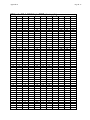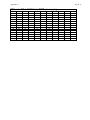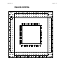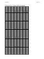
1
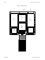
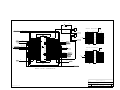
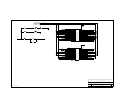
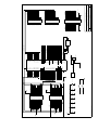
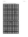
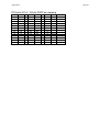
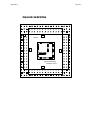
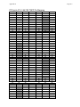
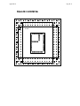
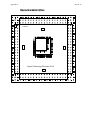
PCCproto 200 User’s Manual M200012-00 April 1996 Preliminary Sycard Technology 1180-F Miraloma Way Sunnyvale, CA 94086 (408) 749-0130 (408) 749-1323 FAX http://www.sycard.com PCCproto 200 User’s Manual Page 1 1.0 Introduction The PCCproto 200 kit is designed to quickly prototype and evaluating a multifunction design based on the National Semiconductor PCM16C02 interface chip. The PCM16C02 is a full 16 bit interface solution for single or multiple function designs. The PCCproto 200 is based on Sycard Technologies PCCproto 150 PC Card prototype platform. Designed specifically for the PC Card development environment, the PCCproto 200 provides support for a wide variety of highpincount, tight pin-pitch devices. PCCproto 200 Key Features: • • • • • • • • • • Integrated National Semiconductor PCM16C02 Multifunction interface chip On-board serial EEPROM for CIS storage On-board oscillator Current Protection Device protect host system Plug-in Daughter boards support a wide variety of high pin count devices Support 4 types of I/O connectors Multilayer construction LEDs indicate Vcc levels Includes 3 general purpose daughter boards PCCswap switch simulates card insertion/removal 1.1 Specifications Electrical Power Current Consumption 3.3V/5.0V Operation 1A max. Mechanical Width Length Thickness Weight 7.7” (19.6 cm) 11.7” (29.7 cm) 0.7” (18mm) 8 oz 1.2 Packing List The PCCproto 200 contains a number of items designed to help in your prototype design. • • • • • • • • M200012-00 PCCproto 200 Main Prototype Board PCCproto 210-1 PCM16C02 Daughter Board PCCproto 210-2 44/100 Pin Prototype Board PCCproto 210-3 100/144/176 Pin Prototype Board PCCproto 210-4 100/144/176 Pin Prototype Board PCCproto Connector Kit - Dual row 0.1" Male Header Assortment - Dual row 0.1” Female Header Assortment PCM16C02 Datasheet - July 1995 PCM16C02 Application Note 975 - January 1995 1996 Sycard Technology Page 2 PCCproto 200 User’s Manual • • • • • PCM16C02 Application Note 976 - January 1995 PCM16C02 Application Note 980 - January 1995 PCCproto 200 User's Manual PCM16C02 Client Source Code License Agreement PCCproto 200 Utility Diskette 1.3 References PC Card Specification, February 1995 Release The PCMCIA Developer's Guide - Second Edition PCM16C02 Datasheet - July 1995 PCM16C02 Application Note 975 - January 1995 PCM16C02 Application Note 976 - January 1995 PCM16C02 Application Note 980 - January 1995 M200012-00 1996 Sycard Technology PCCproto 200 User’s Manual Page 3 2.0 Prototyping with the PCCproto 200 The PCCproto was designed to provide a flexible prototyping environment for PC Card designs. The PCCproto board is divided into several prototype zones. Certain zones accept plug-in daughter boards that support high pin count chips most often found in PC card designs. These high pin count devices are soldered directly onto the daughter board and plugged into the main prototype board. Included in the PCCproto kit are three daughter boards supporting a wide variety of chip types. Section 2.1 describes each zone and which daughter boards are compatible with that zone. Warning - Familiarize yourself with the PCCproto's pin numbering and power supply grid before starting your prototype design. Failure to do so may result in damage to your prototype circuitry and/or your host system. 2.1 PCCproto 200 Main Board The PCCproto 200 consists of several prototype zones: • • • • • • • • PCMCIA host interface Interface Area Prototype Area 1 Prototype Area 2 Prototype Area 3 and 4 Prototype Area 5 and 6 I/O Connector Area Power Grid PCMCIA Host Interface - The PCCproto connects to the PC Card host via a standard Type I interface. All 68 pins can be accessed via two 34 pin connectors at locations J1 and J2. Scope or logic analyzer probes may be connected to these areas. Interface Area - Just past J1 and J2 is the interface area. This area contains the Vcc isolation and over current protection devices. Dual LEDs indicate 3.3V or 5V Vcc levels. A pushbutton switch can be configured to interrupt card detects (CD1 and CD2) to trick the host interface into thinking that the PC Card has been removed. This allows for hot insertion/removal testing without removing the card from the socket. Prototype Area 1 - Prototype area 1 is located at the center of the board. It is designed to accept the main PC Card interface chip (PCM16C02) which is mounted on a plug-in daughter board. Prototype Area 2 - Area 2 is designed to accept a PCCproto 210-x or 210-x daughter board. The 210-x and 210-x allow the user to mount the small TQFP packages typically found on ICs designed for PC Card applications. Prototype Area 3 and 4 - Designed to accept PCCproto 210-x daughter board. The PCCproto 210-x daughter board is designed to accept 44/64/100 pin TQFP or 44/100 pin PQFP packages. Prototype Area 5 and 6 - Designed for traditional devices on 0.1" centers. I/O Connector Area - Three types of I/O connectors are supported in the I/O connector area. The area adjacent to Prototype area 5 support staggered 0.1” connectors. The connector pattern adjacent to Prototype area 6 supports SMT connectors with 0.031" or 0.050" spacing. Next to Prototype area 2 are standard 0.1" dual row locations for standard ribbon type connectors. M200012-00 1996 Sycard Technology M200012-00 WP A3 A5 A7 A15 Vpp1 A4 A6 A12 A16 Vcc D3 D5 GND D4 A10 D7 A11 D6 A8 A9 -OE -CE1 A13 -WE A1 D9 -CD2 BVD1 -REG GND D11 D13 D15 -VS1 -IOWR A18 A20 Vcc A22 A24 -VS2 -CD1 D12 D14 -CE2 -IORD A17 A19 A21 Vpp2 A23 A25 RESET -INPACK -SPKR BVD2 D8 D10 GND Vpp1 Area 5 0.1" Proto Vcc PCM16C02 Board + RDY -IRQ A14 D0 A2 -WAIT D2 A0 GND D1 -IOIS16 Vcc Area 6 0.1" Proto Area 2 0.1" Proto Area 4 0.1" Proto + Area 3 0.1" Proto Offset Pattern 0.1" Straight Pattern SMT Pattern Page 4 PCCproto 200 User’s Manual Figure 2.1-1 PCCproto Layout + + 1996 Sycard Technology PCCproto 200 User’s Manual Page 5 Power Grid - A clearly marked power grid allows access to the Vcc and Ground power planes. The power grid is marked with a silk-screen double line on both the component and circuits side of the board. Vcc is indicated by a diamond shaped pattern while Ground is indicated by a square pad. Bypass capacitors may be mounted between Vcc and ground anywhere in the grid. 2.1.1 Host Interface Area The Host Interface area contains two 34 pin headers (J1 and J2) with the PC Card signals labeled. J1 and J2 can be used to connect a logic analyzer or scope probes. The two headers at J3 and J4 are used to connect the PC Card signals to the PCCproto 210-1 daughter board. The Vcc jumpers (JP5 and JP6) can be used to isolate the prototype’s power from the host system. 5V PWR WP -IOIS16 D1 A0 A2 A4 A6 A12 A16 Vcc -WE A13 A9 -OE -CE1 D6 D4 GND J1 J2 GND -CD2 D2 D9 D0 BVD1 A1 -REG A3 -WAIT A5 -VS2 A7 A24 A15 A22 Vpp1 Vcc RDY A20 -IRQ A14 A18 A8 -IOW R A11 -VS1 A10 D15 D7 D13 D5 D11 D3 GND J3 J4 GND JP5 D10 D8 BVD2 -SPKR JP6 -INPACK RESET A25 A23 Vpp2 R3 A21 A19 A17 -IORD -CE2 D14 D12 -CD1 SW1 CD2 CD1 Figure 2.1-2 Host Interface Area Note: Although J2 and J4 carry the same signals, the pin 1 location on the connectors is mirrored. The PCCswap switch (SW1) can be configured to interrupt the card detect pins (-CD1 and -CD2). Jumpers CD1 and CD2 are described in section 3.4. 2.1.2 I/O connector Area The I/O connector area supports three type of connectors. The SMT pattern routes 0.05” and 0.031” spaced pads to a standard dual row 0.1” header. A dual row 0.1” header accepts a wide variety of solder and wire-wrap headers. M200012-00 1996 Sycard Technology Page 6 PCCproto 200 User’s Manual .050" .031" SMT Pattern 0.1" Pattern Staggered 0.1" Pattern Figure 2.1-3 I/O Connector Area 2.1.3 Power Grid The Power Grid allows access to the Vcc and ground planes. The grid is clearly marked with a double white lines. The Vcc plane is available through the square holes. The ground plane is accessed via the diamond shaped holes. Round holes within the grid are not tied to any plane. Gnd Vcc Figure 2.1-4 Power Grid M200012-00 1996 Sycard Technology PCCproto 200 User’s Manual Page 7 2.2 PCCproto 210-1 National Semiconductor PCM16C02 The PCM16C02 daughter board (PCCproto 210-1) contains the National Semiconductor PCM16C02 and associated circuitry. The 16C02 daughter board is designed to fit within prototype area 1. The PC Card interface signals and power are supplied on connectors J3 and J4 and routed directly to the PCM16C02 chip. The peripheral side of the PCM16C02 chip are accessible through the headers on prototype area 1. P7 JP1 PCM16C02 P6 93C86 OSC P5 Figure 2.2-1 PCCproto 210-1 NSM 16C02 Daughter Board The PCM16C02 daughter board contains a 93C86A serial EEPROM used to store the Card Information Structure (CIS). The serial EEPROM is loaded on power-up into the PCM16C02’s internal RAM memory. The crystal oscillator at U3 supplied the clock required by the PCM16C02. If the designer wishes to use another clock source, it may be disabled by moving the jumper JP1 to pins 2-3. JP1 1-2 2-3 On-board clock External Clock Table 2.2-1 PCCproto 210-1 Clock Select Jumper Information on interfacing and programming the PCM16C02 is included in National Semiconductor’s application and data sheets included with the PCCproto 200 kit. Schematics for the PCCproto 210-1 are located in appendix A of this document. Note: The PCM16C02 is left unconfigured on the PCCproto 200 board. In this unconfigured state it is possible to access internal registers and program the on-board EEPROM. It is up to the user to add their own peripheral circuitry to the prototype board. If used in the unconfigured state, the PCCproto may lockup the host system if the peripheral wait signals or interrupt lines are left unconnected.. M200012-00 1996 Sycard Technology Page 8 PCCproto 200 User’s Manual 2.3 General Purpose Daughter Boards The PCCproto 200 development kit includes three general purpose daughter boards. These boards can accept a wide variety of SMT packages typically used in PC Card applications. Model PCCproto 210-2 PCCproto 210-3 PCCproto 210-4 TQ64 X TQ100 TQ144 TQ176 PQ44 PQ100 X X X X X X X X Table 2.3-1 PCCproto Daughter Boards PQ144 PQ160 X X Since each different daughter board supports several packages, the pinouts of the board will differ depending on the package type. Appendix B lists the pin mapping for all the possible package type and daughter board combinations. Warning: The pinout of the PCCproto 210-2, 210-3 and 210-4 differ depending on the type of IC package used. Carefully follow the pin mappings listed in appendix B or damage to your prototype or host may result. 100/144/176 TQFP Pattern Figure 2.3-1 PCCproto 210-2 Pattern The user may mount devices on either side of the PCCproto 210 boards depending on the pin count and lead pitch of the particular device. Once the devices are mounted, the female headers are mounted on the opposite side of the board. 2.3.1 Connecting Power to the PCCproto 210 All PCCproto 210 boards are of multilayer construction. A separate Vcc and Ground plane provide a low inductance source for the particular chip package. Access to the both the Vcc and Ground planes is provided at the edge of each daughter board. Square (VCC) and Diamond (GND) shaped holes identify the which power plane is attached. These pins may be directly connected to the appropriate pins on the particular chip. Each daughter board contains four surface mount capacitor (1206 size) that are tied between Vcc and Ground that can be used to mount bypass capacitors. M200012-00 1996 Sycard Technology PCCproto 200 User’s Manual Page 9 2.3.2 PCCproto 210-2 The PCCproto 210-2 supports the larger package sizes. One side supports 100, 144 and 176 pin TQFP packages while the other side supports a 160 pin PQFP Package. The 176 pin pinout of the PCCproto 210-2 can be accepted in proto zones 1 and 2. 2.3.3 PCCproto 210-4 The PCCproto 210-4 supports 100 and 144 pin TQFP and 144 pin PQFP Package. The 144 pin pinout of the PCCproto 210-4 can be accepted in proto zones 1 and 2. 2.3.4 PCCproto 210-3 The PCCproto 210-3 supports 64 and 100 pin TQFP on one side and 44 and 100 pin PQFP Package on the other. The 104 pin pinout of the PCCproto 210-3 can be accepted in proto zones 3 and 4. M200012-00 1996 Sycard Technology Page 10 PCCproto 200 User’s Manual 3.0 Prototyping Tips and Hints The PCCproto 200 is designed to provide the designer with a flexible prototyping environment. However, as with any prototype the effects of long wires, poor power distribution and noise may impact your assembly. As with any prototype, proper planning prior to assembly will insure good results with the PCCproto. The following practices will reduce the effects of the prototype construction. Bypass and Bulk Capacitors - Bypass and bulk capacitors may be placed between the Vcc and Ground planes on any of the power access points. Use low ESR (equivalent series resistance) X7R type ceramic capacitors of 0.1uF or greater. For bulk capacitance use tantalum capacitors. Be sure not to over-populate the tantalum capacitors. The inrush current on card power-up may exceed the capability of the Vcc switch on your PC card host. Watch the power distribution - Short paths from the PCCproto’s power planes will reduce the effects of ground bounce and power supply noise. Watch undershoot and overshoot on I/O signals - Under and over-shoot on PC card I/O signals can be a major problem with hardware prototypes. Many CMOS chips are very sensitive to negative undershoot and specify a maximum undershoot of between 0.5 and 0.7V. If your host or you prototype experience large amounts of undershoot, it may be wise to reduce it by using series resistors or some other terminating network. Be aware of the switched power environment of the PC Card interface - The switched power environment of the PC Card interface can cause destructive latchup if. Be extremely careful using external power supplies. - If for any reason an external power supply is used in your prototype insure that the power switched environment of the PC Card interface does not cause a latchup. The designer should consider a relay or some other protection device to prevent destructive latch-up. 3.1 Testing your PC Card implementation There are several steps involved in debugging your PC Card design. The first step is to verify the functionality of the hardware. In order to reduce the number of variables in you hardware debug it is recommended that you disable Socket and Card Services. This can be accomplished by removing these entries in your CONFIG.SYS or AUTOEXEC.BAT. The first step is to open I/O and/or memory windows to your prototype and enable power. To do this the user must be familiar with the architecture of the particular host socket controller. Accessing your host socket controller’s internal registers is often a time consuming and frustrating experience. Most socket controller chip vendors have created socket controller debuggers. These utilities can usually be obtained without charge from your socket controller vendor. Once the windows have been opened, the user may enable the card’s I/O or memory resources through attribute memory space. Once this have been accomplished the hardware can be debugged using any number of traditional debuggers including Microsoft’s DEBUG.EXE. Note: In order to eliminate any possible interactions between your debugger and Socket/Card services disable Card and Socket Services by removing them from your CONFIG.SYS. Once the hardware has been debugged it is time to test your software client implementation with the hardware. Note: Before testing your hardware make sure that your PC Card software is installed properly and works with a variety of similar cards. Testing a client implementation involves inserting and removing a card to verify that the client interacts with Card Services to properly assign resources to your card. By configuring the PCCswap switch, the user may simulate insertion/removals without having to physically pull out the PC Card. M200012-00 1996 Sycard Technology PCCproto 200 User’s Manual Page 11 3.2 Measuring Current Consumption The PCCproto Vcc power plane can be isolated from the host system's power via jumpers JP5 and JP6. When these two jumpers are removed an ammeter can be inserted in series to measure the prototype's power consumption. Warning: Always insure that the slot power is removed before changing the positions of JP5 and JP6. A damaging latch-up condition may occur if CMOS devices are improperly power sequenced. 3.3 Current Protection Device Located at R3 is a Raychem PolySwitch current protection device. This device is designed to protect the host's power supply from a Vcc to ground short on the PCCproto 200. 3.4 Using the PCCswap Switch The PCCswap switch allow the user to momentarily disconnect the -CD1 and -CD2 signals from the PC card prototype. Headers CD1 and CD2 located near the PCCswap switch (SW1) enable operation of the switch. Function CD1 header CD2 header Enable PCCswap 1-2 1-2 Disable PCCswap 2-3 2-3 Table 3.4-1 PCCswap Configuration Jumpers Once the PCCswap switch is enabled, a push of the switch will momentarily de-assert card detects. If Card Services is enabled, it should inform the client of the event and then remove power from the slot. When the switch is released card detects will be re-asserted. Card Services will re-power the slot and notify the client of the insertion event. Note: In a properly configured system, pushing the PCCswap switch will cycle power to the host socket. Before using the PCCswap switch the user should determine if their prototype is immune from latchup problems (see section 3.0). 3.5 Signal Quality Problems One of the most common signal quality problem is over and under shoot on the interface signals. The PC Card Specification dictates that the maximum Vih be no higher than Vcc+0.25 volts and the Vil be no lower than -0.3volts. Operation beyond these limits often times cause unreliable and unexpected errors with the PCCtest series of socket testers. Why the problem? CMOS I/O pins are clamped against Vcc and Ground through protection diodes. When the input voltage exceeds Vcc, the Vcc protection diode will start conducting. The current induced through this clamping action may be quite high (depending on the magnitude over Vcc or below ground). This current may effect adjacent logic areas and cause unpredictable failures. Caution: Do not ignore these failures. While many PC cards are tolerant of such over and undershoots, many are not. M200012-00 1996 Sycard Technology Page 12 PCCproto 200 User’s Manual 4.0 Programming the EEPROM The EEPROM on the PCCproto 210-1 board is used to store PCM16C02 configuration information and the Card Information Structure. The steps involved in creating a Card Information Structure are beyond the scope of this document. Information on creating a CIS is available from a variety of sources including the PCMCIA Developer’s Guide. Once the CIS has been created, it must be programmed in the EEPROM contained on the PCCproto 210-1 board. The PCCproto includes a utility PROTO.EXE that is designed to program a EEPROM connected to the PCM16C02 interface chip. 4.1 Programming the Attribute Memory PROTO.EXE is a MSDOS application used to control the interface and program the EEPROM on the PCCproto 2101. PROTO.EXE is a standalone program designed to run without Card and Socket Services. PROTO.EXE supports a wide variety of socket controller chips. Once the designer has created a binary image of the CIS it is ready to program into the PCM16C02’s EEPROM. Note: PROTO.EXE requires that binary CIS image must be an formatted on byte boundaries. There is no need to insert bytes between each CIS member. The PROTO.EXE is invoked through the following command line: Syntax PROTO -bxx -jx -ax Switches -ax -bxx -jx PCIC Controller address select -a1 = 3E2-3E3H, -a2 = 3E3-3E4H, -a3 = 3E5-3E6H (default = 3E0-3E1H) Select Socket controller xx = Socket controller b10 - Cirrus Logic CL-PD6710/6720 b11 - Cirrus Logic CL-PD6722 b12 - Cirrus Logic CL-PD6729/6730 b20 - Vadem VG-365 b21 - Vadem VG-465/468 b22 - Vadem VG-469 b30 - Intel 82365SL-DF b31 - Intel 82092AA PPEC b40 - Ricoh RF5C266/366 b41 - Ricoh RF5C296/396 b50 - VLSI 82C146 b51 - VLSI 82C146A b60 - Texas Instruments PCI1050 b61 - Texas Instruments PCI1030 b62 - Texas Instruments PCI1130 b70 - Omega Micro b71 - Omega Micro 82094 PCI - PCMCIA b90 - Databook b91 - Databook, ExCA Vpp Control Select alternate memory window. -j1 = C800:0 - CFFF:0, -j2 = E000:0 - E7FF:0 Note: Switches can be entered in any order and must be separated by a space. M200012-00 1996 Sycard Technology Appendix F Page F-1 Appendix A A. Schematics A.1 PCCproto 200 Schematic A.2 PCCproto 210-1 Schematic M200012-00 1996 Sycard Technology SW1 *CDSW PUSHBUTTON CD1 1 2 3 HEADER 3 CD[0..15] CD[0..15] *CD1 1 2 3 4 5 6 7 8 9 10 11 12 13 14 15 16 17 18 19 20 21 22 23 24 25 26 27 28 29 30 31 32 33 34 CD3 CD4 CD5 CD6 CD7 *CE1 *CE1 CA10 *OE *OE VCC *WE/*PGM RDY/*BSY VPP1 WP CA11 CA9 CA8 CA13 CA14 *WE/*PGM RDY/*BSY VPP1 CA16 CA15 CA12 CA7 CA6 CA5 CA4 CA3 CA2 CA1 CA0 CD0 CD1 CD2 WP P1 GND GND CD1 D3 D4 D11 D5 D12 D6 D13 D7 D14 CE1 D15 A10 CE2 OE RFSH IORD A11 A9 IOWR A8 A17 A13 A18 A14 A19 WE/PGM A20 RDY/BSY A21 VCCX VCCX VPP2 VPP1 A22 A16 A23 A15 A24 A12 A25 A7 RFU A6 RESET A5 WAIT A4 A3 INPACK A2 REG A1 BVD2 A0 BVD1 D0 D8 D1 D9 D2 D10 WP CD2 GND GND PCMCIA 35 36 37 38 39 40 41 42 43 44 45 46 47 48 49 50 51 52 53 54 55 56 57 58 59 60 61 62 63 64 65 66 67 68 CD2 1 2 3 HEADER 3 *CD2 *CE2 *IORD *IOWR *CD2 1 3 5 7 9 11 13 15 17 *WE/*PGM 19 CA13 21 CA9 23 *OE 25 *CE1 27 CD6 29 CD4 31 33 J1 1 2 3 4 5 6 7 8 9 10 11 12 13 14 15 16 17 18 19 20 21 22 23 24 25 26 27 28 29 30 31 32 33 34 2 X 17 2 4 6 8 10 12 14 16 18 20 22 24 26 28 30 32 34 CD2 CD0 CA1 CA3 CA5 CA7 CA15 VPP1 RDY/*BSY CA14 CA8 CA11 CA10 CD7 CD5 CD3 VCC VPP2 Test Points VPP2 CA22 CA23 CA24 CA25 VS2 CRESET *WAIT *INPACK *REG BVD2 BVD1 CA[0..25] VCC *CE2 VS1 *IORD *IOWR VS1 CA17 CA18 CA19 CA20 CA21 WP CD1 CA0 CA2 CA4 CA6 CA12 CA16 *CD1 *CD1P CD11 CD12 CD13 CD14 CD15 CD8 CD9 CD10 Test Points *CD2 CD9 BVD1 *REG *WAIT VS2 CA24 CA22 CRESET *WAIT *INPACK *REG BVD2 BVD1 VCC *CD2P VS2 VS2 2 4 6 8 10 12 14 16 18 20 22 24 26 28 30 32 34 CA20 CA18 *IOWR VS1 CD15 CD13 CD11 J2 1 2 3 4 5 6 7 8 10 9 12 11 14 13 16 15 18 17 20 19 22 21 24 23 26 25 28 27 30 29 32 31 34 33 2 X 17 1 3 5 7 9 11 13 15 17 19 21 23 25 27 29 31 33 CD10 CD8 BVD2 *INPACK CRESET CA25 CA23 VPP2 CA21 CA19 CA17 *IORD *CE2 CD14 CD12 *CD1 CA[0..25] HOST SIDE CONNECTOR Sycard Technology Title FILE=PROTO1.S31 PCCproto - Host Connector Size Document Number B 140004 Date: March 21, 1996 Sheet 1 of REV B 2 CA[0..25] CD[0..15] CA[0..25] CD[0..15] 5V LED R1 D1 D2 100 ohm LED 3.3V ZENER R2 D3 220 ohm WP CD1 CA0 CA2 CA4 CA6 CA12 CA16 WP LED POWER LED VCC2 *WE/*PGM VCC R3 VARISTOR JP5 VCC2 *OE *CE1 JUMPER 1 3 5 7 9 11 13 15 17 *WE/*PGM 19 CA13 21 CA9 23 *OE 25 *CE1 27 CD6 29 CD4 31 33 JP6 J3 1 2 3 4 5 6 7 8 9 10 11 12 13 14 15 16 17 18 19 20 21 22 23 24 25 26 27 28 29 30 31 32 33 34 2 X 17 2 4 6 8 10 12 14 16 18 20 22 24 26 28 30 32 34 J4 1 2 3 4 5 6 7 8 10 9 12 11 14 13 16 15 18 17 20 19 22 21 24 23 26 25 28 27 30 29 32 31 34 33 2 X 17 1 3 5 7 9 11 13 15 17 19 21 23 25 27 29 31 33 CD2 CD0 CA1 CA3 CA5 CA7 CA15 VPP1 RDY/*BSY CA14 CA8 CA11 CA10 CD7 CD5 CD3 VPP1 RDY/*BSY JUMPER *CD2 CD9 BVD1 *REG *WAIT VS2 CA24 CA22 BVD1 *REG *WAIT VS2 VCC2 *IOWR VS1 CA20 CA18 *IOWR VS1 CD15 CD13 CD11 2 4 6 8 10 12 14 16 18 20 22 24 26 28 30 32 34 CD10 CD8 BVD2 *INPACK CRESET CA25 CA23 VPP2 CA21 CA19 CA17 *IORD *CE2 CD14 CD12 *CD1 BVD2 *INPACK CRESET VPP2 *IORD *CE2 *CD1 Sycard Technology Title FILE=PROTO2.S31 PCCproto - Host Connector Size Document Number B 140004 Date: March 21, 1996 Sheet 2 of REV B 2 C1 0.1uF *WE HA13 HA9 *OE *CE1 HD6 HD4 1 3 5 7 9 11 13 15 17 19 21 23 25 27 29 31 33 C2 0.1uF C3 0.1uF *CD2 2 HD9 4 *STSCHG/BVD1 6 *REG 8 *WAIT 10 VS2 12 HA24 14 HA22 16 18 HA20 20 HA18 22 *IOWR 24 VS1 26 HD15 28 HD13 30 HD11 32 34 FILE=PIGGYNSM.S31 VCC VCC VCC *IOIS16 HD1 HA0 HA2 HA4 HA6 HA12 HA16 C4 0.1uF P4 1 2 3 4 5 6 7 8 10 9 12 11 14 13 16 15 18 17 20 19 22 21 24 23 26 25 28 27 30 29 32 31 34 33 2 X 17 P3 1 2 3 4 5 6 7 8 9 10 11 12 13 14 15 16 17 18 19 20 21 22 23 24 25 26 27 28 29 30 31 32 33 34 2 X 17 HD[0..15] 1 3 5 7 9 11 13 15 17 19 21 23 25 27 29 31 33 VS2 VS1 C5 0.1uF 0 OHM R2 0 OHM R1 C6 0.1uF HD10 HD8 *SPKR/BVD2 *INPACK CRESET HA25 HA23 VPP2 HA21 HA19 HA17 *IORD *CE2 HD14 HD12 *CD1 2 HD2 4 HD0 6 HA1 8 HA3 10 HA5 12 HA7 14 HA15 16 VPP1 18 20 *IREQ/READY HA14 22 HA8 24 HA11 26 HA10 28 HD7 30 HD5 32 HD3 34 C7 4.7uF 10V 0 OHM R3 5 85 35 57 34 32 33 42 38 37 47 48 49 50 51 52 54 55 59 60 64 62 56 TTL OSC8 OUT U3 *REG *IREQ/READY *INPACK CRESET *WAIT *IOIS16 *STSCHG/BVD1 *SPKR/BVD2 HA0 HA1 HA2 HA3 HA4 HA5 HA6 HA7 HA8 HA9 HA10 HA11 HA12 63 58 65 78 79 80 39 40 41 71 73 74 75 76 HD8 HD9 HD10 HD11 HD12 HD13 HD14 HD15 *OE *WE *CE1 *CE2 *IORD *IOWR 46 45 43 70 69 68 67 66 HD0 HD1 HD2 HD3 HD4 HD5 HD6 HD7 SPK_IN MEMWEH MEMWEL CIORD CIOWR BHE LD8 LD9 LD10 LD11 LD12 LD13 LD14 LD15 LD0 LD1 LD2 LD3 LD4 LD5 LD6 LD7 MCLK0 EESK EECS EEDI/O MCLK1 FCLK1 RIN1 PCNTL1 IOCS16_1 READY1 SRESET1 CINT1 CS1 CWAIT1 MCLK0 FCLK0 RIN0 PCNTL0 IOCS16_0 READY0 SRESET0 CINT0 CS0 CWAIT0 OSC_OUT PCM16C02 TEST0 REG IREQ INPACK RESET HWAIT IOIS16 STSCHG SPKR HA0 HA1 HA2 HA3 HA4 HA5 HA6 HA7 HA8 HA9 HA10 HA11 HA12 HOE HWE CE1 CE2 HIORD HIOWR HD8 HD9 HD10 HD11 HD12 HD13 HD14 HD15 U1 HD0 HD1 HD2 HD3 HD4 HD5 HD6 HD7 EESK EECS EEDI/O JP1 1 2 3 HEADER 3 MCLK0X 82 83 81 MCLK1 FCLK1 RIN1 PCNTL1 *IOCS16_1 READY1 SRESET1 CINT1 *CS1 *CWAIT1 90 89 87 15 91 92 93 94 95 96 SPK_IN *MEMWEH *MEMWEL *CIORD *CIOWR *BHE 1 2 3 LD[0..15] MCLK0X FCLK0 RIN0 PCNTL0 *IOCS16_0 READY0 SRESET0 CINT0 *CS0 *CWAIT0 LD8 LD9 LD10 LD11 LD12 LD13 LD14 LD15 LD0 LD1 LD2 LD3 LD4 LD5 LD6 LD7 24 25 23 14 26 27 28 29 30 31 86 21 22 19 18 17 5 7 8 9 10 11 12 13 97 98 99 100 1 2 3 4 HA[0..25] 93C86A U2 CS DO SK DI ORG 6 4 2 4 6 8 10 12 14 16 18 20 22 24 26 28 30 32 34 36 38 40 1 3 5 7 9 11 13 15 17 19 21 23 25 27 29 31 33 35 1 3 5 7 9 11 13 15 17 19 21 23 25 27 29 31 33 35 1 3 5 7 9 11 13 15 17 19 21 23 25 27 29 31 33 35 37 39 1 3 5 7 9 11 13 15 17 19 21 23 25 27 29 31 33 35 37 39 1 3 5 7 9 11 13 15 17 19 21 23 25 27 29 31 33 35 1 3 5 7 9 11 13 15 17 19 21 23 25 27 29 31 33 35 VCC FCLK1 PCNTL1 READY1 CINT1 *CWAIT1 FCLK0 PCNTL0 READY0 CINT0 *CWAIT0 *MEMWEH *MEMWEL *CIORD HA0 HA1 HA2 HA3 HA4 HA5 HA6 HA7 HA8 HA9 HA10 HA11 HA12 LD15 LD14 LD13 LD12 LD11 LD10 LD9 LD8 LD7 LD6 LD5 LD4 LD3 LD2 LD1 LD0 Sycard Technology 2 X 20 P5 2 4 6 8 10 12 14 16 18 20 22 24 26 28 30 32 34 36 38 40 2 X 18 P7 2 4 6 8 10 12 14 16 18 20 22 24 26 28 30 32 34 36 2 X 18 P6 2 4 6 8 10 12 14 16 18 20 22 24 26 28 30 32 34 36 PCCproto 210-1 PCM16C02 Header Size Document Number B 140005 Date: February 7, 1996 Sheet 1 of Title VCC MCLK1 RIN1 *IOCS16_1 SRESET1 *CS1 MCLK0 RIN0 *IOCS16_0 SRESET0 *CS0 *CIOWR *BHE SPK_IN 2 4 6 8 10 12 14 16 18 20 22 24 26 28 30 32 34 36 2 4 6 8 10 12 14 16 18 20 22 24 26 28 30 32 34 36 REV B 1 Appendix B B. PCCproto Daughter Board Layouts B.1 PCCproto 210-2 176/144/100 TQFP Side Layout B.2 PCCproto 210-2 176/144/100 TQFP Pinouts B.3 PCCproto 210-2 160 PQFP Side Layout B.4 PCCproto 210-2 160 PQFP Pinouts B.5 PCCproto 210-3 64/100 TQFP Side Layout B.6 PCCproto 210-3 64/100 TQFP Pinouts B.7 PCCproto 210-3 44/100 PQFP Side Layout B.8 PCCproto 210-3 44/100 PQFP Pinouts B.9 PCCproto 210-4 144/100 TQFP Side Layout B.10 PCCproto 210-4 144/100 TQFP Pinouts B.11 PCCproto 210-4 144 PQFP Side Layout B.12 PCCproto 210-4 144 PQFP Pinouts Page B-1 Appendix B Page B- 2 PCCproto 210-2 176/144/100 TQFP Side 175 176 173 174 171 169 167 165 163 161 159 157 155 153 151 149 172 170 168 166 164 162 160 158 156 154 152 150 147 148 145 143 141 139 137 135 133 146 144 142 140 138 136 134 1 2 132 131 3 4 130 129 5 6 128 127 7 8 126 125 9 10 124 123 11 12 122 121 13 14 120 119 15 16 118 117 17 18 116 115 19 20 114 113 21 22 112 111 23 24 110 109 25 26 108 107 27 28 106 105 29 30 104 103 31 32 102 101 33 34 100 99 35 36 98 37 38 96 95 39 40 94 93 41 42 92 91 43 44 90 89 Sycard Technology PCCproto 210-2 46 48 50 52 54 56 58 60 62 64 66 68 70 72 74 76 78 80 82 84 86 88 45 47 49 51 53 55 57 59 61 63 65 67 69 71 73 75 77 79 81 83 85 87 97 Appendix B Page B- 3 PCCproto 210-2 100/144/176 TQFP Pin Mapping Header 1 2 3 4 5 6 7 8 9 10 11 12 13 14 15 16 17 18 19 20 21 22 23 24 25 26 27 28 29 30 31 32 33 34 35 36 37 38 39 40 41 42 43 44 45 46 47 48 49 50 TQ100 TQ144 TQ176 1 1 1 2 2 2 3 3 3 4 4 4 5 5 5 6 6 6 7 7 7 8 8 8 9 9 9 10 10 10 11 11 11 12 12 12 13 13 13 14 14 14 15 15 15 16 16 16 17 17 17 18 18 18 19 19 19 20 20 20 21 21 21 22 22 22 23 23 23 24 24 24 25 25 25 26 26 27 27 28 28 29 29 30 30 31 31 32 32 33 33 34 34 35 35 36 36 37 38 39 40 41 42 43 44 26 37 45 27 38 46 28 39 47 29 40 48 30 41 49 31 42 50 Header TQ100 TQ144 TQ176 61 42 53 61 62 43 54 62 63 44 55 63 64 45 56 64 65 46 57 65 66 47 58 66 67 48 59 67 68 49 60 68 69 50 61 69 70 70 71 71 72 72 73 73 74 74 75 75 76 76 77 77 78 78 79 79 80 80 81 81 82 82 83 83 84 84 85 85 86 86 87 87 88 88 89 89 90 90 91 91 92 92 93 93 94 94 95 95 96 96 97 97 98 98 99 99 100 100 101 101 102 102 103 103 104 104 105 105 106 106 107 107 108 51 84 108 109 52 85 109 110 53 86 110 Header TQ100 TQ144 TQ176 120 63 96 120 121 64 97 121 122 65 98 122 123 66 99 123 124 67 100 124 125 68 101 125 126 69 102 126 127 70 103 127 128 71 104 128 129 72 105 129 130 73 106 130 131 74 107 131 132 75 108 132 133 133 134 134 135 135 136 136 137 137 138 138 139 139 140 140 141 109 141 142 110 142 143 111 143 144 112 144 145 113 145 146 114 146 147 115 147 148 116 148 149 117 149 150 118 150 151 119 151 152 76 120 152 153 77 121 153 154 78 122 154 155 79 123 155 156 80 124 156 157 81 125 157 158 82 126 158 159 83 127 159 160 84 128 160 161 85 129 161 162 86 130 162 163 87 131 163 164 88 132 164 165 89 133 165 166 90 134 166 167 91 135 167 168 92 136 168 169 93 137 169 Appendix B Page B- 4 PCCproto 210-2 100/144/176 TQFP Pin Mapping Header v51 52 53 54 55 56 57 58 59 60 TQ100 TQ144 TQ176 32 43 51 33 44 52 34 45 53 35 46 54 36 47 55 37 48 56 38 49 57 39 50 58 40 51 59 41 52 60 Header TQ100 TQ144 TQ176 111 54 87 111 112 55 88 112 113 56 89 113 114 57 90 114 115 58 91 115 116 59 92 116 117 60 93 117 118 61 94 118 119 62 95 119 120 63 96 120 Header TQ100 TQ144 TQ176 170 94 138 170 171 95 139 171 172 96 140 172 173 97 141 173 174 98 142 174 175 99 143 175 176 100 144 176 Appendix B Page B- 5 PCCproto 210-2 160 PQFP Side 175 173 171 169 167 165 163 176 174 172 170 168 166 164 161 162 159 157 155 153 151 149 160 158 156 154 152 150 147 148 145 143 141 139 137 135 133 146 144 142 140 138 136 134 1 2 132 3 4 130 5 6 128 7 8 126 125 9 10 124 123 11 12 122 121 13 14 120 119 15 16 118 117 17 18 116 115 19 20 114 113 21 22 112 111 23 24 110 109 25 26 108 107 27 28 106 105 29 30 104 103 31 32 102 101 33 34 100 99 35 36 98 37 38 96 95 39 40 94 93 41 42 92 91 43 44 90 89 46 48 50 52 54 56 58 60 62 64 66 68 70 72 74 76 78 80 82 84 86 88 45 47 49 51 53 55 57 59 61 63 65 67 69 71 73 75 77 79 81 83 85 87 131 129 127 97 Appendix B Page B- 6 PCCproto 210-2 160 pin PQFP pin mapping Header 1 2 3 4 5 6 7 8 9 10 11 12 13 14 15 16 17 18 19 20 21 22 23 24 25 26 27 28 29 30 31 32 33 34 35 36 37 38 39 40 41 42 43 44 45 46 47 48 PQ160 1 2 3 4 5 6 7 8 9 10 11 12 13 14 15 16 17 18 19 20 21 22 23 24 25 26 27 28 29 30 31 32 33 34 35 36 37 38 39 40 41 42 Header 61 62 63 64 65 66 67 68 69 70 71 72 73 74 75 76 77 78 79 80 81 82 83 84 85 86 87 88 89 90 91 92 93 94 95 96 97 98 99 100 101 102 103 104 105 106 107 108 PQ160 55 56 57 58 59 60 61 62 63 64 65 66 67 68 69 70 71 72 73 74 75 76 77 78 79 80 81 82 83 84 85 86 87 88 89 90 91 92 93 94 95 96 97 98 Header PQ160 121 111 122 112 123 113 124 114 125 115 126 116 127 117 128 118 129 119 130 120 131 132 133 134 135 121 136 122 137 123 138 124 139 125 140 126 141 127 142 128 143 129 144 130 145 131 146 132 147 133 148 134 149 135 150 136 151 137 152 138 153 139 154 140 155 141 156 142 157 143 158 144 159 145 160 146 161 147 162 148 163 149 164 150 165 151 166 152 167 153 168 154 Appendix B Page B- 7 PCCproto 210-2 160 pin PQFP pin mapping Header 49 50 51 52 53 54 55 56 57 58 59 60 PQ160 43 44 45 46 47 48 49 50 51 52 53 54 Header 109 110 111 112 113 114 115 116 117 118 119 120 PQ160 99 100 101 102 103 104 105 106 107 108 109 110 Header PQ160 169 155 170 156 171 157 172 158 173 159 174 160 175 176 Appendix B Page B- 8 PCCproto 210-3 64/100 TQFP Side 1 2 3 4 5 103 101 99 97 95 93 91 89 87 85 83 81 79 104 102 100 98 96 94 92 90 88 86 84 82 80 78 77 76 75 6 74 73 7 8 72 9 10 70 11 12 68 13 14 66 65 15 16 64 63 17 18 62 61 19 20 60 59 21 22 58 57 23 24 56 55 25 26 54 53 64/100 Sycard Technology PCCproto 210-3 28 27 30 29 32 34 36 38 40 42 44 46 48 50 31 33 35 37 39 41 43 45 47 49 52 51 71 69 67 Appendix B Page B- 9 PCCproto 210-3 64/100 TQFP Pin Mapping Header 1 2 3 4 5 6 7 8 9 10 11 12 13 14 15 16 17 18 19 20 21 22 23 24 25 26 27 28 29 30 31 32 33 34 35 36 37 38 39 40 41 42 43 44 45 46 47 48 TQ64 1 2 3 4 5 6 7 8 9 10 11 12 13 14 15 16 TQ100 1 2 3 4 5 6 7 8 9 10 11 12 13 14 15 16 17 18 19 20 21 22 23 24 25 18 17 27 26 29 28 31 30 33 32 35 34 37 36 39 38 41 40 43 42 45 44 47 46 20 19 22 21 24 23 26 25 28 27 30 29 32 31 Header 53 54 55 56 57 58 59 60 61 62 63 64 65 66 67 68 69 70 71 72 73 74 75 76 77 78 79 80 81 82 83 84 85 86 87 88 89 90 91 92 93 94 95 96 97 98 99 100 TQ64 33 34 35 36 37 38 39 40 41 42 43 44 45 46 47 48 49 51 50 53 52 55 54 57 56 59 58 61 60 TQ100 51 52 53 54 55 56 57 58 59 60 61 62 63 64 65 66 67 68 69 70 71 72 73 74 75 77 76 79 78 81 80 83 82 85 84 87 86 89 88 91 90 93 92 95 94 97 96 Appendix B Page B- 10 PCCproto 210-3 64/100 TQFP Pin Mapping Header 49 50 51 52 TQ64 TQ100 49 48 50 Header 101 102 103 104 TQ64 63 62 TQ100 99 98 64 104 Appendix B Page B- 11 PCCproto 210-3 44/100 PQFP Side 1 103 101 99 97 95 93 91 89 87 85 83 81 79 104 102 100 98 96 94 92 90 88 86 84 82 80 2 44/100 78 77 3 4 76 75 5 6 74 73 7 8 72 9 10 70 11 12 68 13 14 66 65 15 16 64 63 17 18 62 61 19 20 60 59 21 22 58 57 23 24 56 55 25 26 54 53 28 27 30 29 32 34 36 38 40 42 44 46 48 50 31 33 35 37 39 41 43 45 47 49 52 51 71 69 67 Appendix B Page B- 12 PCCproto 210-3 44/100 side Header 1 2 3 4 5 6 7 8 9 10 11 12 13 14 15 16 17 18 19 20 21 22 23 24 25 26 27 28 29 30 31 32 33 34 35 36 37 38 39 40 41 42 43 44 45 46 47 48 PQ44 1 2 3 4 5 6 7 8 9 10 11 12 13 14 15 16 17 18 19 20 21 22 PQ100 1 2 3 4 5 6 7 8 9 10 11 12 13 14 15 16 17 18 19 20 21 22 23 24 25 27 26 29 28 31 30 33 32 35 34 37 36 39 38 41 40 43 42 45 44 47 46 Header 53 54 55 56 57 58 59 60 61 62 63 64 65 66 67 68 69 70 71 72 73 74 75 76 77 78 79 80 81 82 83 84 85 86 87 88 89 90 91 92 93 94 95 96 97 98 99 100 PQ44 23 24 25 26 27 28 PQ100 51 52 53 54 55 56 57 58 59 60 61 62 63 64 65 66 67 68 69 70 71 72 73 74 75 35 34 37 36 39 38 41 40 77 76 79 78 81 80 83 82 85 84 87 86 89 88 91 90 93 92 95 94 97 96 Appendix B Page B- 13 PCCproto 210-3 44/100 side Header 49 50 51 52 PQ44 PQ100 49 48 50 Header 101 102 103 104 PQ44 43 42 PQ100 99 98 44 100 Appendix B Page B- 14 PCCproto 210-4 100/144 TQFP Side 1 2 3 143 141 139 137 135 133 131 129 127 125 123 121 119 117 115 144 142 140 138 136 134 132 130 128 126 124 122 120 118 116 113 114 111 112 109 110 108 107 4 106 105 6 104 103 7 8 102 101 9 10 100 99 11 12 98 97 13 14 96 95 94 93 15 100/144 16 17 18 92 19 20 90 89 21 22 88 87 23 24 86 85 25 26 84 83 27 28 82 29 30 31 32 33 34 35 36 Sycard Technology PCCproto 210-4 40 42 37 39 41 44 43 46 48 50 52 45 47 49 51 54 53 56 58 60 62 64 66 55 57 59 61 63 65 68 67 70 72 69 71 81 80 79 78 77 76 75 74 38 91 73 Appendix B Page B- 15 PCCproto 210-4 100/144 pin TQFP pin mapping Header 1 2 3 4 5 6 7 8 9 10 11 12 13 14 15 16 17 18 19 20 21 22 23 24 25 26 27 28 29 30 31 32 33 34 35 36 37 38 39 40 41 42 43 44 45 46 47 TQ100 1 2 3 4 5 6 7 8 9 10 11 12 13 14 15 16 17 18 19 20 21 22 23 24 25 26 27 28 29 30 31 32 33 34 35 36 TQ144 1 2 3 4 5 6 7 8 9 10 11 12 13 14 15 16 17 18 19 20 21 22 23 24 25 26 27 28 29 30 31 32 33 34 35 36 37 38 39 40 41 42 43 44 45 46 47 Header 61 62 63 64 65 66 67 68 69 70 71 72 73 74 75 76 77 78 79 80 81 82 83 84 85 86 87 88 89 90 91 92 93 94 95 96 97 98 99 100 101 102 103 104 105 106 107 TQ100 50 51 52 53 54 55 56 57 58 59 60 61 62 63 64 65 66 67 68 69 70 71 72 73 74 TQ144 61 62 63 64 65 66 67 68 69 70 71 72 73 74 75 76 77 78 79 80 81 82 83 84 85 86 87 88 89 90 91 92 93 94 95 96 97 98 99 100 101 102 103 104 105 106 107 Header 121 122 123 124 125 126 127 128 129 130 131 132 133 134 135 136 137 138 139 140 141 142 143 144 TQ100 77 78 79 80 81 82 83 84 85 86 87 88 89 90 91 92 93 94 95 96 97 98 99 100 TQ144 121 122 123 124 125 126 127 128 129 130 131 132 133 134 135 136 137 138 139 140 141 142 143 144 Appendix B Page B- 16 PCCproto 210-4 100/144 pin TQFP pin mapping Header 48 49 50 51 52 53 54 55 56 57 58 59 60 TQ100 37 38 39 40 41 42 43 44 45 46 47 48 49 TQ144 48 49 50 51 52 53 54 55 56 57 58 59 60 Header 108 109 110 111 112 113 114 115 116 117 118 119 120 TQ100 75 76 TQ144 108 109 110 111 112 113 114 115 116 117 118 119 120 Header TQ100 TQ144 Appendix B Page B- 17 PCCproto 210-4 144 PQFP Side 143 141 139 137 135 133 131 129 127 125 123 121 119 117 115 144 142 140 138 136 134 132 130 128 126 124 122 120 118 116 113 114 111 112 109 110 1 2 108 107 3 4 106 105 6 104 103 7 8 102 101 9 10 100 99 11 12 98 97 13 14 96 95 94 93 15 16 17 18 92 19 20 90 89 21 22 88 87 23 24 86 85 25 26 84 83 27 28 82 29 30 80 79 31 32 78 77 33 34 76 75 35 36 74 38 40 42 37 39 41 44 43 46 48 50 52 45 47 49 51 54 53 56 58 60 62 64 66 55 57 59 61 63 65 68 67 70 72 69 71 91 81 73 Appendix B Page B- 18 PCCproto 210-4 144 pin PQFP pin mapping Header 1 2 3 4 5 6 7 8 9 10 11 12 13 14 15 16 17 18 19 20 21 22 23 24 25 26 27 28 29 30 31 32 33 34 35 36 37 38 39 40 41 42 43 44 45 46 47 48 49 PQ144 1 2 3 4 5 6 7 8 9 10 11 12 13 14 15 16 17 18 19 20 21 22 23 24 25 26 27 28 29 30 31 32 33 34 35 36 37 38 39 40 41 42 43 44 45 46 47 48 49 Header 61 62 63 64 65 66 67 68 69 70 71 72 73 74 75 76 77 78 79 80 81 82 83 84 85 86 87 88 89 90 91 92 93 94 95 96 97 98 99 100 101 102 103 104 105 106 107 108 109 PQ144 61 62 63 64 65 66 67 68 69 70 71 72 73 74 75 76 77 78 79 80 81 82 83 84 85 86 87 88 89 90 91 92 93 94 95 96 97 98 99 100 101 102 103 104 105 106 107 108 109 Header 121 122 123 124 125 126 127 128 129 130 131 132 133 134 135 136 137 138 139 140 141 142 143 144 PQ144 121 122 123 124 125 126 127 128 129 130 131 132 133 134 135 136 137 138 139 140 141 142 143 144 Appendix B Page B- 19 PCCproto 210-4 144 pin PQFP pin mapping Header 50 51 52 53 54 55 56 57 58 59 60 PQ144 50 51 52 53 54 55 56 57 58 59 60 Header 110 111 112 113 114 115 116 117 118 119 120 PQ144 110 111 112 113 114 115 116 117 118 119 120 Header PQ144 Appendix C Page C-1 C. Ordering Additional PCCproto Modules Additional PCCproto daughter boards may be ordered directly from Sycard Technology. The following boards are available: Model Number PCCproto 210-2 PCCproto 210-3 PCCproto 210-4 Supports 44/64/100 TQFP 44/100 PQFP 64/100/144 TQFP 144 PQFP 100/144/176 TQFP 160 PQFP Appendix D D. The PCM16C02 Utility Diskette The PCM16C02 utility diskette includes several files 1. Orcad schematics PCCproto 210-1 2. Orcad schematics PCCproto 200 Main Board 3. Orcad Library element for PCM16C02 Page D-1 Appendix E Page E-1 Appendix E - PCMCIA Interface PC Card Pinout - Memory Mode Pin Name Description Pin Name Description 1 2 3 4 5 6 7 8 9 10 11 12 13 14 15 16 17 18 GND D3 D4 D5 D6 D7 CE1# A10 OE# A11 A9 A8 A13 A14 WE# READY VCC VPP1 35 36 37 38 39 40 41 42 43 44 45 46 47 48 49 50 51 52 GND CD1# D11 D12 D13 D14 D15 CE2# VS1# RFU RFU A17 A18 A19 A20 A21 VCC VPP2 A16 A15 A12 A7 A6 A5 A4 A3 A2 A1 Ground Data Bit 3 Data Bit 4 Data Bit 5 Data Bit 6 Data Bit 7 Card Enable 1 Address Bit 10 Output Enable Address Bit 11 Address Bit 9 Address Bit 8 Address Bit 13 Address Bit 14 Write Enable Ready/Busy Card Power Programming Supply Voltage 1 Address Bit 16 Address Bit 15 Address Bit 12 Address Bit 7 Address Bit 6 Address Bit 5 Address Bit 4 Address Bit 3 Address Bit 2 Address Bit 1 53 54 55 56 57 58 59 60 61 62 A22 A23 A24 A25 VS2# RESET WAIT# RFU REG# BVD2 29 A0 Address Bit 0 63 BVD1 30 31 32 33 34 D0 D1 D2 WP GND Data Bit 0 Data Bit 1 Data Bit 2 Write Protect Ground 64 65 66 67 68 D8 D9 D10 CD2# GND Ground Card Detect 1 Data Bit 11 Data Bit 12 Data Bit 13 Data Bit 14 Data Bit 15 Card Enable 2 Voltage Sense 1 Reserved Reserved Address Bit 17 Address Bit 18 Address Bit 19 Address Bit 20 Address Bit 21 Card Power Programming Supply Voltage 2 Address Bit 22 Address Bit 23 Address Bit 24 Address Bit 25 Voltage Sense 2 Card Reset Extend Bus Cycle Reserved Register Select Battery Voltage Detect 2 Battery Voltage Detect 1 Data Bit 8 Data Bit 9 Data Bit 10 Card Detect 2 Ground 19 20 21 22 23 24 25 26 27 28 Appendix E Page E- 2 PC Card Pinout - I/O Mode Pin Name Description Pin Name Description 1 2 3 4 5 6 7 8 9 10 11 12 13 14 15 16 17 18 GND D3 D4 D5 D6 D7 CE1# A10 OE# A11 A9 A8 A13 A14 WE# IREQ# VCC VPP1 35 36 37 38 39 40 41 42 43 44 45 46 47 48 49 50 51 52 GND CD1# D11 D12 D13 D14 D15 CE2# VS1# IORD# IOWR# A17 A18 A19 A20 A21 VCC VPP2 19 20 21 22 23 24 25 26 A16 A15 A12 A7 A6 A5 A4 A3 Ground Data Bit 3 Data Bit 4 Data Bit 5 Data Bit 6 Data Bit 7 Card Enable 1 Address Bit 10 Output Enable Address Bit 11 Address Bit 9 Address Bit 8 Address Bit 13 Address Bit 14 Write Enable Interrupt Request Card Power Programming Supply Voltage 1 Address Bit 16 Address Bit 15 Address Bit 12 Address Bit 7 Address Bit 6 Address Bit 5 Address Bit 4 Address Bit 3 53 54 55 56 57 58 59 60 A22 A23 A24 A25 VS2# RESET WAIT# INPACK# 27 A2 Address Bit 2 61 REG# 28 A1 Address Bit 1 62 SPKR# 29 30 31 32 33 34 A0 D0 D1 D2 IOIS16# GND Address Bit 0 Data Bit 0 Data Bit 1 Data Bit 2 IO Port is 16 bits Ground 63 64 65 66 67 68 STSCHG# D8 D9 D10 CD2# GND Ground Card Detect 1 Data Bit 11 Data Bit 12 Data Bit 13 Data Bit 14 Data Bit 15 Card Enable 2 Voltage Sense 1 I/O Read Strobe I/O Write Strobe Address Bit 17 Address Bit 18 Address Bit 19 Address Bit 20 Address Bit 21 Card Power Programming Supply Voltage 2 Address Bit 22 Address Bit 23 Address Bit 24 Address Bit 25 Voltage Sense 2 Card Reset Extend Bus Cycle Input Port Acknowledge Register and I/O select enable Digital Audio Waveform Card Status Changed Data Bit 8 Data Bit 9 Data Bit 10 Card Detect 2 Ground Appendix F Page F-1 Appendix F - Connector Drawings Pin 1 Pin 34 Surface A Surface B Pin 35 Pin 68 Pin 34 Pin 1 Pin 68 Pin 35 #1 #33 #34 #2 #67 #35 #36 #68 INSERT CARD #33 #1 #34 #2 #67 #35 #36 #68 INSERT CARD