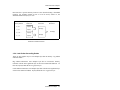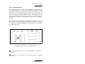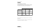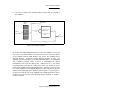
1
Model 618, 618-9U &
620 Adapters
Hardware Manual
Connect a PCI Computer
to a VMEbus System
Model 618 & 620 Adapters
2
Model 618 & 620 Adapters
Disclaimer
Please read and abide by the following paragraphs. Questions and comments
should be directed to:
Technical Publications Department
SBS Technologies, Inc.
Connectivity Products
1284 Corporate Center Drive
St. Paul, MN 55121-1245
651-905-4700
SBS Technologies does not authorize the use of its components in life support
applications where failure or malfunction of the component may result in injury
or death. In accordance with SBS's terms and conditions of sale, the user of
SBS components in any and all life support applications assumes all risks
arising out of such use and further agrees to indemnify and hold SBS harmless
against any and all claims of whatsoever kind or nature (including claims of
culpable conduct [strict liability, negligence or breach of warranty] on the part
of SBS) for all costs of defending any such claims.
SBS does not authorize the use of its components in control and process
applications where failure or malfunction of the component may result in
radioactive releases, explosions, environmental damage/contamination,
personal injury or death. In accordance with SBS's terms and conditions of
sale, the user of SBS components in any and all control and process
applications assumes all risks arising out of such use and further agrees to
indemnify and hold SBS harmless against any and all claims of whatsoever kind
or nature (including claims of culpable conduct [strict liability, negligence or
breach of warranty] on the part of SBS) for all costs of defending any such
claims.
SBS makes no warranty of any kind with regard to this material, including, but
not limited to, the implied warranties of merchantability and fitness for a
particular purpose. SBS assumes no responsibility for any errors that may
appear in this document. The information in this document is subject to change
without notice.
3
Model 618 & 620 Adapters
U.S. GOVERNMENT LIMITED RIGHTS
This documentation is provided with limited rights. Use, duplication or
disclosure by the Government is subject to the restrictions as set forth in
subdivision (b) (3) (iii) of the Rights in Technical Data and Computer Software
Clause of DFAR252.227-7013 (October 1988) and in similar clauses in the
FAR and NASA FAR Supplement. Manufacturer is SBS Technologies, Inc.,
Connectivity Products, 1284 Corporate Center Drive, St. Paul, MN 551211245.
Copyright © 1998, 1999 by SBS Technologies, Inc. Portions reprinted with
permission of the PCI Special Interest Group.
Revision 1.5
9/99
Pub. No. 85851150
4
Model 618 & 620 Adapters
Preface
This manual describes SBS Model 618, Model 618-9U, and Model 620
adapters that connect a PCI bus system to a VMEbus system via fiber-optic
cable. It includes information about the adapters’ operation, installation,
configuration, and control registers.
Models 618 and 620 are physically and functionally identical with one
exception. Model 618 adapters have a loopback diagnostic feature for PIO
transfers; Model 620 does not.
In this manual all references to Model 618 apply to Models 618, 618-9U, and
620. If any text refers to just one of the models, that model will be identified by
“Model 618 only”, “Model 618-9U only”, or “Model 620 only”.
To simplify installation and eliminate operation problems, SBS recommends
that you review this manual before beginning to install your new adapter cards.
Please pay close attention to the sections on card configuration and adapter
registers.
Chapter 1 provides an overview of the adapter, product description,
specifications and requirements, and supporting products.
Chapter 2 gets you started with information about unpacking the adapter
package, adapter installation, Help, and additional references.
Chapter 3 discusses basic bus issues, features that are common to both
adapter cards, and cable conflict issues.
Chapter 4 provides a broad overview of the PCI adapter card, including
how the major features fit together and how they are used. This chapter
also introduces the various memory windows.
Chapter 5 talks about how to use PCI adapter card functions, including
making VMEbus accesses, allowing VMEbus accesses, handling interrupts,
initiating a DMA operation from PCI, and configuration registers.
5
Model 618 & 620 Adapters
Chapter 6 describes Control and Status Registers (CSR) accessed from the
PCI bus.
Chapter 7 is an overview of the VMEbus adapter card.
Chapter 8 deals with using the VMEbus adapter card functions, such as:
making accesses to PCI, allowing PCI accesses, handling interrupts, and
initiating a DMA operation from VMEbus.
Chapter 9 describes Control and Status Registers (CSR) accessed from the
VMEbus.
Chapter 10 contains details for setting jumpers on the VMEbus adapter
card.
Chapter 11 provides suggestions and solutions for common problems with
setting up and using the adapter.
Appendix A is a glossary of terms used throughout this manual.
Appendix B provides information about VMEbus addressing, including pin
assignments and address modifiers.
Appendix C discusses PCI BIOS functions.
Appendix D contains a jumper configuration worksheet.
Important Notes:
Make sure you follow proper ESD handling procedures (refer to EIA-625,
ESD Association Handbook, or MIL-HDBK-263) when working with
cards and components.
Be sure power is OFF before installing adapter cards.
Please read this manual thoroughly before trying to install or use the
adapter.
6
Model 618 & 620 Adapters
Table Of Contents
Chapter 1: Introduction .............................................................................15
1.0 Overview ............................................................................................ 15
1.1 Adapter Features................................................................................. 18
1.2 Supporting Products ........................................................................... 20
1.2.1 Cables................................................................................ 20
1.2.2 Dual Port RAM ................................................................. 21
1.2.3 Model 618-9U ................................................................... 21
1.3 System Controller Operation .............................................................. 21
1.4 Adapter Control And Status Registers (CSRs) ................................... 22
1.5 Direct Memory Access (DMA) .......................................................... 22
1.6 Interrupts ............................................................................................ 23
1.7 Mapping Registers.............................................................................. 23
Chapter 2: Getting Started ........................................................................25
2.0 Unpacking .......................................................................................... 25
2.1 Help!................................................................................................... 26
2.2 Installation .......................................................................................... 26
2.2.1 Configure The Adapter Cards ........................................... 26
2.2.2 Installing The PCI Adapter Card....................................... 27
2.2.3 Installing The VMEbus Adapter Card............................... 27
2.2.4 Connecting The Adapter Cable ......................................... 28
2.3 Additional References ........................................................................ 29
Chapter 3: The Model 618 Adapter...........................................................31
3.0 Introduction ........................................................................................ 31
3.1 PCI Bus .............................................................................................. 31
3.2 VMEbus ............................................................................................. 31
3.2.1 System Controller Operation............................................. 32
3.2.2 Backplane Jumpers............................................................ 33
3.2.3 VMEbus Address Modifiers.............................................. 34
3.2.4 VMEbus Interrupts And The IACK Cycle ........................ 35
3.3 Bridging PCI And VMEbus ............................................................... 36
3.3.1 Programmed Interrupt To Transmitter (PT) ...................... 38
3.3.2 Programmed Interrupt To Receiver (PR) .......................... 39
3.3.3 Direct Memory Access (DMA) ......................................... 40
7
Model 618 & 620 Adapters
3.3.4 How Controller Mode DMA Transfers Occur .................. 41
3.3.5 Slave Mode DMA ............................................................. 42
3.4 Accessing Windows............................................................................ 43
3.5 Byte And Word Swapping.................................................................. 44
3.5.1 Data Accesses.................................................................... 44
3.5.2 Little Endian Versus Big Endian....................................... 45
3.5.3 Swapping For Byte Accesses ............................................ 46
3.5.4 Swapping For Word Accesses........................................... 47
3.5.5 Longword Accesses........................................................... 49
3.5.6 Access Width Versus Data Width ..................................... 50
3.6 Loopback – Models 618 & 618-9U Only -......................................... 51
3.6.1 External Loopback – Model 618-9U Only........................ 52
Chapter 4: The PCI Adapter Card ............................................................ 53
4.0
4.1
4.2
4.3
4.4
4.5
Introduction ........................................................................................ 53
Configuration Registers ...................................................................... 54
PCI CSR ............................................................................................. 55
Mapping Registers.............................................................................. 56
Remote Memory Window .................................................................. 57
PCI Adapter Card LEDs..................................................................... 58
Chapter 5: Using PCI Adapter Card Functions ...................................... 59
5.0
5.1
5.2
5.3
Introduction ........................................................................................ 59
Finding And Mapping the Adapter ..................................................... 59
Initialization........................................................................................ 60
Accessing Remote Memory................................................................ 60
5.3.1 VMEbus Memory.............................................................. 61
5.3.2 Dual Port RAM ................................................................. 61
5.3.3 Mapping Register Window ............................................... 62
5.3.3.1 Remote Memory Mapping Register Format..... 63
5.3.4 PCI To VMEbus Address.................................................. 64
5.3.5 Example of Accessing VMEbus........................................ 65
5.4 Allowing VMEbus Accesses .............................................................. 66
5.4.1 Setting Up PCI Memory.................................................... 67
5.4.2 VMEbus Remote RAM Window ...................................... 67
5.4.3 Mapping Register Window ............................................... 68
5.4.3.1 VMEbus-To-PCI Bus Mapping Register
Format........................................................................... 70
5.4.4 Example: Allowing VMEbus Accesses............................ 71
8
Model 618 & 620 Adapters
5.5 Handling Interrupts............................................................................. 72
5.5.1 Programmed Interrupts...................................................... 73
5.5.1.1 Sending PT Interrupts ...................................... 74
5.5.1.2 Receiving PT Interrupts ................................... 75
5.5.1.3 Sending PR Interrupts ...................................... 75
5.5.1.4 Receiving PR Interrupts ................................... 75
5.5.2 Error Interrupts.................................................................. 76
5.5.3 VMEbus Backplane Interrupts .......................................... 77
5.5.4 DMA Interrupts................................................................. 78
5.5.5 Writing An Interrupt Service Routine ............................... 78
5.6 Initiating A DMA Operation .............................................................. 79
5.6.1 Mapping Register Window ............................................... 80
5.6.1.1 DMA-To-PCI Bus Mapping Register
Format........................................................................... 82
5.6.2 DMA CSRs ....................................................................... 83
5.6.3 Other CSRs........................................................................ 84
5.6.4 DMA Transfer Modes ....................................................... 85
5.6.5 When Is The DMA Operation Done?................................ 85
5.6.5.1 DMA Done Interrupt........................................ 85
5.6.5.2 Polling For DMA Done Bit.............................. 86
5.6.6 Programming Sequence For Initiating A DMA Transfer
From PCI..................................................................................... 87
5.6.7 Things To Remember........................................................ 88
5.6.8 Example Of Initiating A DMA Operation ......................... 88
5.7 Configuration Registers ...................................................................... 91
5.7.1 Finding And Identifying The PCI Adapter Card ............... 92
5.7.1.1 Vendor ID Register ........................................... 92
5.7.1.2 Device ID Register........................................... 92
5.7.1.3 Revision ID Register........................................ 92
5.7.1.4 Class Code Register ......................................... 93
5.7.2 Where Are The Windows? ................................................ 93
5.7.2.1 I/O Mapped Node I/O Base
Address Register ........................................................... 94
5.7.2.2 Memory Mapped Node I/O Base
Address Register ........................................................... 94
5.7.2.3 Mapping Register Base Address
Register ......................................................................... 95
5.7.2.4 Remote Memory Base Address
Register ......................................................................... 96
9
Model 618 & 620 Adapters
5.7.3 Other Registers.................................................................. 96
5.7.3.1 Command Register........................................... 96
5.7.3.2 Status Register ................................................. 98
5.7.3.3 Interrupt Line Register ..................................... 100
Chapter 6: CSR Accessed From The PCI Bus........................................ 101
6.0 CSR Accessed From The PCI Bus ..................................................... 101
6.1 Local Node Registers ......................................................................... 102
6.1.1 Local Command Register .................................................. 102
6.1.2 Interrupt Control Register ................................................. 103
6.1.3 Local Status Register......................................................... 104
6.1.4 Interrupt Status Register.................................................... 106
6.1.5 PCI Control Register ......................................................... 106
6.1.6 PCI Loopback Control Register –Models 618 & 6189U Only-...................................................................................... 107
6.2 Remote Node Registers ...................................................................... 108
6.2.1 Remote Command Register 1............................................ 109
6.2.2 Remote Status Register ..................................................... 111
6.2.3 Remote Command Register 2............................................ 112
6.2.4 Adapter ID Register .......................................................... 113
6.2.5 Remote VMEbus Address Modifier Register.................... 113
6.2.6 Remote IACK Read Registers........................................... 114
6.3 DMA Controller Registers.................................................................. 114
6.3.1 DMA Controller and Error Status Registers Accessed
From The PCI Bus ...................................................................... 115
6.3.2 Local DMA Controller Command Register....................... 116
6.3.3 Local DMA Remainder Count Register ............................ 117
6.3.4 Local DMA Packet Count Register ................................... 117
6.3.5 Local DMA PCI Address Register .................................... 118
6.3.6 Remote DMA Controller Remainder Count Register........ 118
6.3.7 Remote DMA VMEbus Address Registers ....................... 118
6.3.8 Slave Status Register ......................................................... 119
Chapter 7: The VMEbus Adapter Card .................................................... 121
7.0
7.1
7.2
7.3
7.4
10
Introduction ........................................................................................ 121
VMEbus Adapter Card Jumper Blocks .............................................. 122
VMEbus CSR ..................................................................................... 123
Remote RAM Window....................................................................... 123
Dual Port RAM Window.................................................................... 124
Model 618 & 620 Adapters
7.5 VMEbus System Controller Mode ..................................................... 125
7.6 VMEbus Adapter Card LEDs............................................................. 127
Chapter 8: Using VMEbus Adapter Card Functions...............................129
8.0 Introduction ........................................................................................ 129
8.1 Initialization........................................................................................ 129
8.2 Accessing PCI Memory...................................................................... 129
8.2.1 Remote RAM Jumpers ...................................................... 130
8.2.2 Interaction with Mapping Registers .................................. 130
8.3 Accessing Dual Port RAM ................................................................. 131
8.4 Allowing PCI Accesses ...................................................................... 131
8.5 Handling Interrupts............................................................................. 132
8.5.1 Programmed Interrupts...................................................... 133
8.5.1.1 Sending PT Interrupts ...................................... 133
8.5.1.2 Receiving PT Interrupts ................................... 133
8.5.1.3 Sending PR Interrupts ...................................... 134
8.5.1.4 Receiving PR Interrupts ................................... 134
8.5.2 Error Interrupts.................................................................. 135
8.5.3 DMA Interrupts................................................................. 136
8.5.4 Sending Backplane Interrupts To PCI............................... 136
8.5.5 Writing An ISR ................................................................. 137
8.6 Initiating A DMA Operation .............................................................. 138
8.6.1 PCI Initialization ............................................................... 138
8.6.2 DMA CSRs ....................................................................... 139
8.6.3 Other CSRs........................................................................ 141
8.6.4 When Is The DMA Operation Done?................................ 141
8.6.4.1 DMA Done Interrupt........................................ 141
8.6.4.2 Polling For DMA Done Bit.............................. 142
8.6.5 Programming Sequence For Initiating A DMA
From VMEbus............................................................................. 142
8.6.6 Things To Remember........................................................ 144
Chapter 9: CSR Accessed From The VMEbus ........................................145
9.0 VMEbus CSR ..................................................................................... 145
9.1 Local Node Registers ......................................................................... 146
9.1.1 Loopback Register – Models 618 & 618-9U Only - ......... 146
9.1.2 Local Command Register .................................................. 147
9.1.3 Local Status Register......................................................... 148
9.1.4 Address Modifier Register ................................................ 149
9.1.5 Interrupt Vector Register................................................... 149
11
Model 618 & 620 Adapters
9.2 Remote Node Registers ...................................................................... 150
9.2.1 Remote Command Register............................................... 150
9.2.2 Remote Status Register ..................................................... 151
9.2.3 PCI Adapter ID Register ................................................... 152
9.3 DMA Controller Registers.................................................................. 152
9.3.1 DMA Controller Registers Accessed From The
VMEbus ...................................................................................... 152
9.3.2 Local DMA Controller Command Register....................... 153
9.3.3 Local DMA Remainder Count Register ............................ 155
9.3.4 Local DMA VMEbus Address Register ............................ 155
9.3.5 Local DMA Packet Count Registers ................................. 156
9.3.6 Remote DMA Remainder Count Register ......................... 156
9.3.7 Remote DMA PCI Address Registers ............................... 156
Chapter 10: Setting The VMEbus Adapter Card Jumpers..................... 159
10.0 Introduction ...................................................................................... 159
10.1 Configuration Notes ......................................................................... 159
10.1.1 VMEbus Adapter Card Diagram..................................... 160
10.2 VMEbus Adapter Card Factory Settings .......................................... 161
10.3 VMEbus Adapter Card Jumper Blocks ............................................ 161
10.3.1 System Jumpers............................................................... 162
10.3.2 Bus Grant And Bus Request Jumpers.............................. 163
10.3.3 I/O Range Jumpers .......................................................... 166
10.3.4 Remote RAM Jumpers .................................................... 167
10.3.5 Dual Port RAM Jumpers ................................................. 170
10.3.6 Transmitted Interrupt Jumpers ........................................ 173
10.3.7 Received Interrupt Jumpers............................................. 174
10.3.8 Address Bias Jumpers ..................................................... 174
10.4 Setting Jumpers For System Controller Mode.................................. 175
Chapter 11: Common Problems .............................................................. 179
11.0 Introduction ...................................................................................... 179
11.1 Software Problems............................................................................ 179
11.1.1 Data Order Is Incorrect.................................................... 179
11.1.2 Dual Port RAM Alignment ............................................. 180
11.1.3 Bus Error Or Unexpected Status ID
(Interrupt Vector) Returned When Reading IACK
Read Register .............................................................................. 181
12
Model 618 & 620 Adapters
11.1.4 Programming Issues ........................................................ 181
11.1.4.1 Volatile .......................................................... 182
11.1.4.2 Accessing Addresses Above One
Megabyte ...................................................................... 182
11.1.4.3 Making D32 Accesses.................................... 182
11.2 Hardware Problems .......................................................................... 183
11.2.1 Using The VMEbus Adapter Card LEDs As
Diagnostic Tools ......................................................................... 183
11.2.2 Error In The Local Status Register.................................. 184
11.2.2.1 Local Status Register Bit 7: Interface Data
Error.............................................................................. 184
11.2.2.2 Local Status Register Bit 6: Remote Bus
Error.............................................................................. 185
11.2.2.3 Local Status Register Bit 2: Interface
Timeouts ....................................................................... 187
11.2.2.4 Local Status Register Bit 0: Cable
Disconnected................................................................. 188
11.2.3 PCI Motherboards ........................................................... 188
11.2.3.1 Cache ............................................................. 188
11.2.3.2 PCI Slots ........................................................ 189
11.2.3.3 Concurrent Accesses ...................................... 189
Appendix A: Glossary................................................................................191
Appendix B: VMEbus References ............................................................195
B.1 VMEbus Pin Assignments ................................................................. 195
B.2 VMEbus Address Modifier Codes..................................................... 197
Appendix C: PCI BIOS Functions.............................................................199
C.1 Identifying PCI Resources ................................................................. 199
C.1.1 PCI BIOS Present ............................................................. 199
C.1.2 Find PCI Device ............................................................... 200
C.2 Accessing Configuration Space ......................................................... 201
C.2.1 Read Configuration Byte .................................................. 201
C.2.2 Read Configuration Word................................................. 202
C.2.3 Read Configuration Longword ......................................... 203
C.2.4 Write Configuration Word................................................ 204
13
Model 618 & 620 Adapters
Appendix D: Jumper Configuration Worksheet ..................................... 205
Index............................................................................................................ 207
14
Model 618 & 620 Adapters
Chapter 1: Introduction
Models 618 and 620 are physically and functionally identical with one
exception. Model 618 adapters have a loopback diagnostic feature for PIO
transfers; Model 620 does not.
In this manual all references to Model 618 apply to Models 618, 618-9U,
and 620. If any text refers to just one of the models, that model will be
identified by “Model 618 only”, “Model 618-9U only”, or “Model 620
only”.
1.0 Overview
Model 618 – the next generation for SBS’s market accepted and widely used
Model 617 Adapter – is the most cost-effective solution for applications
requiring VMEbus to PCI connectivity and fiber-optic capabilities. By
eliminating the need for Fiber-Optic Interface Modules, Model 618 provides
the benefits of fiber-optics and increases system reliability. Fewer components
are required for fiber-optic capabilities than with the Model 617. Plus,
applications written for Model 617 can easily port to Model 618.
With Model 618 you can use a standard PC or workstation instead of a single
board computer thereby letting you take advantage of a wealth of off-the-shelf
software, the latest processor technology, and worldwide support form major
PC, workstation and operating system manufacturers. Consequently, effectively
speeding your development effort and reducing time to market.
Model 618’s fiber-optic features make it ideal for environments requiring noise
immunity, high-performance, electrical safety, isolation and long distance
system separation.
The adapter allows you to share memory and special purpose boards between a
PCI Local Bus computer and a VMEbus system. The adapter provides highspeed data transfers between systems, and requires minimal software support.
Introduction 15
Model 618 & 620 Adapters
Model 618 interconnects the PCI and VMEbus systems at the physical layer.
Working at the lowest level, the bus, the adapter allows the two systems to
share memory; memory appears to and is treated by each system as if it were its
own. Therefore, a card only available on one bus may be accessed and directly
controlled by a system using another bus. For example, an Array Processor
board in a VMEbus chassis can be directly controlled by the processor on the
PCI bus.
Model 618 supports two methods of intersystem communications: Memory
Mapping and Direct Memory Access (DMA). Memory Mapping supports bidirectional random access bus mastering from either system. This allows
Programmed Input/Output (PIO) access to VMEbus RAM, dual-port memory,
and VMEbus I/O, and provides an easy-to-use, flexible interface with low
overhead. A PCI bus master can access memory in the VMEbus system
through a window in PCI memory address space. Conversely, a VMEbus bus
master can access PCI memory from a window in VMEbus address space.
Memory mapping is accomplished through 16,384 Mapping Registers that are
used to steer memory accesses on one bus to the appropriate address on the
other bus. The Mapping Registers allow PCI devices to access up to 32M bytes
of VMEbus address space and VMEbus devices to access up to 16M bytes of
PCI space. In addition, the Mapping Registers allow up to 16M byte DMA
transfers.
The Model 618 adapter supports two DMA techniques: Controller Mode DMA
and Slave Mode DMA.
Controller Mode DMA uses the adapter's DMA Controller to provide
high-speed data transfers from one system's memory directly into the other
system's memory. Data transfer can be initiated in both directions by either the
PCI or VMEbus processor. Each DMA cycle supports transfer lengths up to
16M bytes. The DMA Controller also allows memory-to-memory transfers
between PCI memory and Dual Port RAM on the VMEbus adapter card.
Controller Mode DMA can sustain data rates up to 35 Megabytes per second
(M Bytes/sec).
16 Introduction
Model 618 & 620 Adapters
VMEbus devices that have their own DMA controllers can use Slave Mode
DMA instead of Controller Mode DMA. Slave Mode DMA allows a VMEbus
DMA device to transfer data through the adapter directly into PCI memory at
data rates in excess of 15M Bytes/sec.
Model 618 does not link the timing of the two buses (so that activity on one bus
slows down the other). Instead, the adapter permits each bus to operate
independently. The buses are linked only when a memory or I/O reference is
made to an address on one system that translates to a reference on the other
system's bus.
The Model 618 adapter consists of two cards: a short form factor PCI card and
a 6U size VMEbus card. The two cards are connected by fiber-optic cable
purchased separately from SBS.
Cable is available in standard 10-meter or 25-meter lengths. Custom lengths
may be ordered.
An optional Dual Port RAM card that installs on the VMEbus adapter card is
available from SBS. The Dual Port RAM can be accessed by both systems and
provides an inexpensive method of expanding PCI and VMEbus memory as
well as a convenient way to share memory between the two systems. The
following Dual Port RAM sizes are available: 128K and 8M bytes.
Introduction 17
Model 618 & 620 Adapters
1.1 Adapter Features
Bus Communication Specifics:
Both adapter cards are capable of remote bus mastership and allow
simultaneous communication between the two chassis (except when a DMA
transfer is in progress).
The PCI adapter card responds to and generates A32 memory and I/O accesses
and supports D32, D16, and D8 data widths (Mapping Registers support only
D32 and D16; CSRs support only D16 and D8).
The VMEbus adapter card responds to and generates A32, A24, and A16
accesses and supports D32, D16, and D8 data widths (A16 space supports only
D16 and D8). D32 and D16 Block Mode transfers are also supported.
The VMEbus adapter card accepts and can generate all address modifier codes
except VME64.
System Controller: The VMEbus adapter card can provide the system clock,
reset, and bus error timeout feature.
Bus Arbitration: Provides Single-Level (SGL) or four-level Priority/RoundRobin (PRI/RRS) arbitration.
VMEbus:
Release-On-Request (ROR);
Release-On-Bus-Clear.
Access Times:
PCI bus read/write access to remote RAM: about 1.8 µsec.
PCI bus read/write access to remote Dual Port RAM: about 1.7 µsec.
VMEbus read/write access to local Dual Port RAM: 400 nsec.
Slave Mode DMA Transfer Rate:
VMEbus Block Mode access to PCI RAM -VMEbus writes to PCI bus: about 15M Bytes/sec.
VMEbus reads from PCI bus: about 14M Bytes/sec.
18 Introduction
Model 618 & 620 Adapters
DMA Controller Transfer Rate*:
* This rate may vary significantly depending on PCI chip set implementation.
The adapter is capable of sustained DMA data rates of:
35M Bytes/sec with 20 nsec Block Mode VMEbus memory cards;
20M Bytes/sec with 50 nsec Block Mode VMEbus memory cards;
10M Bytes/sec with 200 nsec Block Mode VMEbus memory cards;
13M Bytes/sec DMA from PCI bus to Dual Port RAM.
Actual data rates measured from the application software level are also
dependent on the clock frequency of the PCI I/O channel controller and system
software overhead.
DMA data transfer block length: 2 bytes to 16M bytes.
Interrupt Passing:
All seven VMEbus interrupts can be passed to the PCI system.
Two types of programmed interrupts (PT and PR Interrupts) can be exchanged
between the PCI adapter card and the VMEbus.
Interrupt Acknowledgment:
RORA (Release On Register Access).
PCI acknowledgment of VMEbus interrupts and VMEbus vector passing is
provided through an adapter card control register.
PCI - VMEbus Timeout:
PCI bus to VMEbus transfer cycles timeout within 30 µsec. This results in an
error bit being set and an interrupt generated if enabled.
Read-Modify-Write:
Read-modify-write from the PCI to the VMEbus system is supported via the
PCI interface signal LOCK# and a CSR bit.
Read-modify-write from the VMEbus system into PCI memory is not
supported.
Read-modify-write transactions to dual-port memory are also supported.
Introduction 19
Model 618 & 620 Adapters
Conformance:
The VMEbus adapter card meets IEEE 1014C specifications.
The PCI card meets the PCI Local Bus specification version 2.0.
Power Requirements:
The VMEbus adapter card draws 4.0A at 5V.
The PCI adapter card draws 2.0A at 5V.
Environment:
Temperature:
Humidity:
0º to 60º C operating;
-40º to 85º C storage.
0% to 90% non-condensing.
1.2 Supporting Products
Cables to connect the two adapter cards, and Dual Port RAM cards are also
available from SBS. Please call 651-905-4700 for more information.
1.2.1 Cables
Fiber-optic cables to connect the two adapter cards consist of 50 µm multimode
fiber with duplex SC connectors. Cables are available in 10-meter and 25meter lengths. Custom-length cables up to 500 meters are also available from
SBS. All cables are purchased separately.
20 Introduction
Model 618 & 620 Adapters
1.2.2 Dual Port RAM
Dual Port RAM is an optional memory card that attaches to the VMEbus
adapter card and appears to both systems as simply more memory. The address
of the Dual Port RAM is independently set on each adapter card, and may be
set to respond to one address range in one system and a different range in the
other. Both systems can access the memory at the same time with the VMEbus
adapter card arbitrating simultaneous accesses.
SBS's Dual Port RAM is a printed circuit card that plugs into the VMEbus
adapter card as a daughter card. The following memory sizes are currently
available: 128K and 8M bytes.
1.2.3 Model 618-9U
Model 618-9U is a Model 618 adapter with the 6U size VMEbus card installed
in a 9U holder that allows the card to be installed in 9U card slot. Model 618
functions identically to Model 618.
1.3 System Controller Operation
The Model 618 adapter can act as a link between a PCI chassis and a VMEbus
chassis even when the VMEbus chassis has no processor or system controller
present. This form of operation is called System Controller Mode.
System Controller Mode is configured by setting the VMEbus adapter card's
SYS jumper block to drive the system clock (SYSCLK) and the Bus Error
(BERR) global timeout. The SBS VMEbus adapter card may be configured to
be a Single-Level (SGL) bus arbiter or a four-level bus arbiter in Priority (PRI)
or Round-Robin (RRS) mode.
Introduction 21
Model 618 & 620 Adapters
1.4 Adapter Control And Status Registers (CSRs)
The CSRs allow PCI and VMEbus bus masters to control and obtain status
information about the adapter. Each system has 32 CSRs that the adapter can
access; half the CSRs are located on the local adapter card and half on the
remote adapter card. VMEbus processors can access the VMEbus CSRs
through 32 bytes of VMEbus I/O space. PCI processors can use either I/O
space or PCI memory space to access their 32 CSRs.
1.5 Direct Memory Access (DMA)
DMA is the transfer of data from one memory address to another without
processor intervention once the transfer starts. DMA logic is usually employed
when large files or sections of data need to be moved.
The Model 618 adapter supports two types of DMA operations: Controller
Mode DMA and Slave Mode DMA. In Controller Mode DMA, the adapter
becomes a bus master on both the PCI bus and the VMEbus, and transfers data
from memory on one system to memory on the other system. Controller Mode
DMA transfers require very little processor attention and are a very fast means
of transferring data.
Slave Mode DMA is performed when a VMEbus DMA device, such as a disk
controller card, does a block transfer through the adapter directly into the PCI
bus. In this case, the VMEbus adapter card looks like a slave memory card.
22 Introduction
Model 618 & 620 Adapters
1.6 Interrupts
The adapter has four sources of interrupts; three can be generated by either
adapter card, one is unique to the PCI adapter card.
Common interrupt sources:
Programmed Interrupts - Each adapter card can receive and send a
programmed interrupt from the other adapter card. Programmed interrupts
are the basic method processors on the two dissimilar buses use to
communicate and synchronize data transfers. There are two types of
programmed interrupts: Programmed interrupt to Transmitter (PT) and
Programmed interrupt to Receiver (PR).
Interface Error Interrupt - Each adapter card can assert an interrupt when it
detects that an error occurred.
DMA Done Interrupt - Each adapter card can interrupt a local processor
when the DMA has completed.
PCI adapter card specific interrupt source:
VMEbus Backplane Interrupt - The PCI adapter card can interrupt the PCI
bus whenever any of seven VMEbus interrupt levels are asserted. The
adapter also allows a PCI processor to acknowledge the VMEbus interrupt
and retrieve the interrupt acknowledgment vector.
1.7 Mapping Registers
The PCI adapter card is equipped with Mapping Registers that allow the
adapter to take a large contiguous section of local memory and map it to many
small non-contiguous sections of remote memory. This feature is very
desirable because most of today's system architectures use virtual and paged
memory management schemes. These schemes often satisfy an application's
memory request with small sections of memory that are scattered throughout
the memory space. The Mapping Registers allow a bus-to-bus bridge to remap
these non-contiguous memory areas into a contiguous areas on the remote bus.
This mapping works both for PCI to VMEbus accesses and VMEbus to PCI
accesses.
Introduction 23
Model 618 & 620 Adapters
24 Introduction
Model 618 & 620 Adapters
Chapter 2: Getting Started
Make sure you follow proper ESD handling procedures (refer to EIA-625,
ESD Association Handbook, or MIL-HDBK-263) when working with
cards and components.
2.0 Unpacking
The SBS Model 618 adapter package contains the following items. Please
identify each item and notify SBS (651-905-4700) if any are missing.
Models 618 & 618-9U:
PCI circuit card Part Number: 85851090
VMEbus circuit card Part Number: 85853432 or
Model 618-9U card installed in holder Part Number: 82920251
Software Drivers CD-ROM Part Number: 84702000
Model 618 manual Pub. Number: 85851150
One I/O cable to connect the two cards (purchased separately)
Warranty card (please complete and mail)
Models 620:
PCI circuit card Part Number: 85851093
VMEbus circuit card Part Number: 85853435
Software Drivers CD-ROM Part Number: 84702000
Model 618 manual Pub. Number: 85851150
One I/O cable to connect the two cards (purchased separately)
Warranty card (please complete and mail)
Eight-digit part numbers with card revision level are printed on white
labels affixed to the adapter cards.
Getting Started 25
Model 618 & 620 Adapters
2.1 Help!
Please have the following items and information handy when calling SBS for
technical support:
Model number and revision level of the adapter, or the serial number
located on the white bar code label on the adapter cards.
Size of Dual Port RAM, if any.
Configuration information including jumper settings on the VMEbus
adapter card. Record the jumper settings on the diagram in Appendix D.
This manual.
Technical support is available from 9:00 a.m. - 5:00 p.m. (Central Time)
Monday - Friday, excluding holidays.
Contact SBS at:
Mailing Address:
SBS Technologies, Inc.
Connectivity Products
1284 Corporate Center Drive
St. Paul, MN 55121-1245
Phone:
651-905-4700
Fax:
651-905-4701
Email:
[email protected]
Web:
www.sbs.com
2.2 Installation
Observe static safety precautions to prevent damage to the cards.
Make sure power is off before installing cards.
2.2.1 Configure The Adapter Cards
Any required jumper configuration takes place before the adapter cards are
installed. Refer to Chapter 10 for information about configuring the VMEbus
adapter card. There are no jumpers to configure on the PCI adapter card.
26 Getting Started
Model 618 & 620 Adapters
2.2.2 Installing The PCI Adapter Card
1.
Locate a vacant PCI card slot in the PCI chassis that supports a bus master.
2.
Remove the metal plate that covers the cable exit at the rear of the chassis.
3.
Insert the PCI adapter card into the connector.
4.
Fasten the adapter card in place with the mounting screw.
2.2.3 Installing The VMEbus Adapter Card
VMEbus backplanes have jumpers to connect the daisy-chained, bus grant
and interrupt acknowledge signals around unused card locations. Make
sure these jumpers are removed from the slot in which the adapter card will
be installed.
1.
Decide if the VMEbus adapter card is the system controller. If it is, it must
be installed in slot 1.
2.
Locate an unoccupied 6U slot* in the VMEbus card cage if the adapter
card is not the system controller.
* The Model 618-9U VMEbus card/holder installs in a 9U slot.
3.
Insert the card into the connector of the selected slot.
Getting Started 27
Model 618 & 620 Adapters
2.2.4 Connecting The Adapter Cable
Keep the ends of the fiber-optic cable clean. Use alcohol-based fiber-optic
wipes to remove minor contaminants such as dust and dirt.
Fiber-optic cables are made of glass; therefore, they may break if crushed
or bent in a loop with less than a 2-inch radius.
To connect the I/O cable:
1.
Make sure the PCI computer system and the VMEbus chassis are powered
off.
2.
Remove the rubber boots on the fiber-optic transceivers as well as the ones
on the fiber-optic cables. Be sure to replace these boots when cables are
not in use.
3.
Plug one end of the fiber-optic cable into the PCI adapter card’s
transceiver.
4.
Plug the other end of the fiber-optic cable into the VMEbus adapter card’s
transceiver.
5.
Turn power on to both PCI and VMEbus systems.
After installation, make sure the READY LEDs on both adapter cards are
lit. They must be on for the adapter to operate.
28 Getting Started
Model 618 & 620 Adapters
2.3 Additional References
The VMEbus Specification Manual is available from VITA (VMEbus
International Trade Association), 7825 E. Gelding Drive, Suite 104,
Scottsdale, AZ 85260-3415.
IEEE Standard 1014 is available from The Institute of Electrical and
Electronics Engineers (IEEE), 445 Hoes Lane, Piscataway, NJ
08855-1331.
The PCI Local Bus Specification is available from the PCI Special Interest
Group, JF2-51, 5200 NE Elam Young Parkway, Hillsboro, OR 971246497.
PCI BIOS Specification is available from the PCI Special Interest Group,
JF2-51, 5200 NE Elam Young Parkway, Hillsboro, OR 97124-6497.
DOS Protected Mode Interface (DPMI) Specification Version 1.0 is
available from Intel Corp.
Data Format and Bus Compatibility in Multiprocessors, IEEE Micro,
August 1983, is available from IEEE Micro, PO Box 3014, Los Alamitos,
CA 90720-1264.
Getting Started 29
Model 618 & 620 Adapters
30 Getting Started
Model 618 & 620 Adapters
Chapter 3: The Model 618 Adapter
3.0 Introduction
The Model 618 adapter functions as a bridge between the PCI bus and
VMEbus. The adapter allows PCI bus masters to become masters on the
VMEbus, and VMEbus master to become masters on the PCI bus.
Because the adapter interconnects two dissimilar buses, it is important to
understand both buses. Chapter 3 discusses basic bus issues, features that are
common to both adapter cards, and cable conflict issues.
3.1 PCI Bus
The PCI bus is a 32-bit architecture designed for high-data throughput, selfconfiguration, and multiple bus mastership.
The PCI bus is self-configuring; therefore, all PCI devices are automatically
configured by the startup firmware at system boot. The startup firmware sets up
interrupt level routing and other hardware parameters, and resolves all
addressing conflicts. Simply plug the PCI device into an open PCI slot and
switch on the power; the system takes care of configuration.
The PCI specification supports multiple bus masters on the PCI bus.
Consequently, the adapter allows VMEbus masters to become bus masters on
the PCI bus, and supports Direct Memory Access (DMA) data transfers.
3.2 VMEbus
The VMEbus is a 32-bit bus that is widely used in industrial, commercial and
military applications worldwide. An abundance of VMEbus cards are available
to perform a wide range of tasks, from digital image processing to disk
controllers. Like the PCI bus, the VMEbus supports multiple bus masters and
high data transfer rates. Unlike the PCI bus, the VMEbus is not selfconfiguring.
The Model 618 Adapter 31
Model 618 & 620 Adapters
A VMEbus consists of card cage with 1 - 21 slots, a backplane with two
connectors and, normally, five jumpers per slot. The slots are numbered from 1
- 21. Slot 1 is the system controller slot. Cards with different functions are
inserted in the slots to form a customized VMEbus chassis.
Sections 3.2.1 - 3.2.4 discuss several important unique VMEbus features:
system controller operation, backplane jumpers, interrupt acknowledgment
cycle, and address spaces.
3.2.1 System Controller Operation
A card that provides system controller functions must be installed in slot 1 of
the VMEbus card cage. The system controller (usually a processor card)
provides bus arbitration, checks for timeouts, and drives the system clock and
system reset signals. The SBS VMEbus adapter card may be configured to be a
Single-Level (SGL) bus arbiter or a four-level bus arbiter in Priority (PRI) or
Round-Robin (RRS) mode.
The Model 618 adapter has the ability to act as a link between a PCI chassis
and a VMEbus chassis even when the VMEbus chassis has no processor
present. This form of operation is called System Controller Mode. System
Controller Mode is selected on the VMEbus adapter card by configuring the
SYS and BGO-BGI jumper blocks. These jumpers tell the VMEbus adapter
card that it must provide the system controller functions, including: bus
arbitration, timeout detection, and system level signals. See Chapter 10 for
detailed descriptions of VMEbus adapter card jumper blocks.
A priority arbiter provides requesters preferential control of the data transfer
bus over the other levels. By definition, BR3 is the highest priority, and BR0 is
the lowest. When two or more requests are pending, the arbiter assigns control
of the bus in the appropriate order by granting the bus in this sequence.
The priority arbiter must assert BCLR when a bus master of higher priority than
the one in control of the bus initiates a request. When BBSY is asserted and a
request is pending, the arbiter will drive BCLR if the pending request is of
higher priority than the bus grant of the previous arbitration. Although the
current bus master is not required to relinquish control of the bus in any
prescribed time limit, it can continue transferring data until it reaches an
appropriate stopping point.
32 The Model 618 Adapter
Model 618 & 620 Adapters
A round-robin arbiter gives equal priority to all bus request levels. It grants
control of the bus on a rotating basis. Upon release of the bus, the arbiter steps
one level and tests for an active request and asserts a bus grant. If no request is
active, it continues stepping through the levels until a request is found.
The RRS arbiter can drive the BCLR signal. In RRS mode BCLR is asserted
whenever a master requests the bus on a level other than the last one granted. It
does not assert BCLR if a master on the same level requests the bus.
There must be one and only one card with System Controller Mode
enabled. This card must be installed in slot 1.
When the VMEbus adapter card is in System Controller Mode, except in
special situations, the SYSCLK and SYSRESET jumpers must be installed.
In most cases, the Detect Bus Timeout jumper should also be installed.
3.2.2 Backplane Jumpers
VMEbus chassis have five jumpers associated with each slot except slot 1. The
five jumpers pass the bus grant and interrupt acknowledge signals to the next
slot. If a slot is empty, the jumpers must be installed in order to pass the daisychained signals to the next slot. For example, if slots 1, 5 and 7 have cards
installed, slots 2, 3, 4, and 6 must have the backplane jumpers installed or the
system will not function properly.
If a slot has no card installed and a card is installed in higher number slot,
the backplane jumpers must be installed in the empty slot.
Backplane jumpers should never be installed in slots in which cards are
installed.
The Model 618 Adapter 33
Model 618 & 620 Adapters
3.2.3 VMEbus Address Modifiers
The VMEbus specification defines three types of address spaces: extended
(A32), standard (A24) and short (A16). Extended (A32) addressing uses 32
address bits. Standard (A24) addressing uses 24 address bits. Short (A16)
addressing uses 16 address bits. The VMEbus uses special lines, the address
modifier lines, to select which type of address space is being referenced.
Although the adapter does not respond to VME64 address modifiers, it can still
be used in VME64 systems to do D32, D16, or D8 transfers with A32, A24, or
A16 address modifiers.
Each address space is independent of the other address spaces and can be
thought of as a logically separate address bus. A32 addressing uses address
lines A31-01. A24 uses A23-01, and A31-24 are unused. A16 uses A15-A01,
and A31-16 are unused. The VMEbus does not have an address 0 (A0) line.
Byte addressing is controlled by the signals DS0 and DS1. Address lines A03A01 are used during Interrupt ACKnowledge cycles (IACK cycles).
The following table summarizes the use of the address bus.
ACTIVE PORTION OF ADDRESS BUS - ADDRESS ROUTING
A31 - A24 A23 - A16
A15 - A04
A03 - A01
Address Modifier
Codes (hex)
A31 ---------------------------------------------------A01
Extended (32-bit)
08 - 0F
A23------------------------------------A01
Standard (24-bit)
38 - 3F
A15-------------------A01
Short I/O (16-bit)
29, 2D
A03 - A01
Interrupt
Acknowledge
= Unused portion of address bus.
The value of the address modifier lines, AM[0..5], determines which address
space is used. The VMEbus master is responsible for supplying the proper
address modifier at the same time it drives the address lines. Slaves are
designed to respond to cycles with a particular address modifier; however, most
slaves are capable of responding to several address modifiers.
34 The Model 618 Adapter
Model 618 & 620 Adapters
The address modifier generated when the PCI bus accesses the VMEbus is
determined by the value in the selected Mapping Register. The programmer
should determine which address modifier the target slave responds to, then
program the Mapping Registers with that value.
The most commonly used address modifier codes are listed below. For a
complete list of address modifiers, see Appendix B.
ADDRESS
MODIFIER (HEX)
NUMBER OF
ADDRESS BITS
TRANSFER TYPE
2D
3D
3F
0D
0F
16
24
24
32
32
Short supervisory access
Standard supervisory access
Standard supervisory block transfer
Extended supervisory data access
Extended supervisory block transfer
The VMEbus adapter card can generate and respond to all address
modifiers except D64.
3.2.4 VMEbus Interrupts And The IACK Cycle
Hardware devices use interrupts to indicate that they need attention or that
some event has occurred. The VMEbus supports seven interrupt levels labeled
IRQ1 to IRQ7. Any number of devices can use the same interrupt; however,
only one VMEbus device can respond to an interrupt level.
Interrupts are responded to with an IACK cycle. The basic interrupt process is
as follows:
1.
A VMEbus device asserts one of the seven interrupt lines.
example, we assume IRQ1.
For this
2.
The VMEbus device acknowledging IRQ1 receives control of the VMEbus
and starts a byte, word, or longword read with the IACK signal asserted.
This read should have address bits A3 - A1 equal to the level of the
interrupt to be acknowledged. For example, IRQ1 is acknowledged by
reading from location 2 (A3=0, A2=0, A1=1).
The Model 618 Adapter 35
Model 618 & 620 Adapters
3.
The system controller starts the IACK daisy-chain by sending IACKIN to
slot 2. This daisy-chained IACK signal is passed up the slots until it
reaches the card asserting IRQ1.
4.
The device asserting IRQ1 responds to the IACK read cycle with the
appropriate size data (the status/id value or IACK read vector).
5.
The VMEbus device uses the IACK read vector to determine which device
is interrupting and makes any necessary accesses to the interrupting
device's registers to acknowledge the interrupt.
Two types of interrupting devices are supported by the VMEbus: Release On
AcKnowledgment (ROAK) and Release On Register Access (RORA). A
ROAK device removes its interrupt near the end of the IACK cycle (see step 4
above). A RORA device removes its interrupt after the IACK cycle occurred
and one of its registers is accessed (see step 5).
For RORA devices, software must make a register access to switch off the
interrupt before exiting the Interrupt Service Routine (ISR). Otherwise, the
interrupting device will not remove its interrupt and the processor will go into
an endless IACK loop.
3.3 Bridging PCI And VMEbus
The PCI and VMEbus adapter cards are connected by a cable that carries
commands from one card to the other. Unless there is a software cable control
scheme, it is possible for both cards to send commands at the same time. Since
the PCI bus supports retry and the VMEbus (Rev. C) does not, the PCI adapter
card usually gives precedence to VMEbus commands. The adapter responds to
the PCI bus master with a target retry response and allows the VMEbus
command to proceed. Ideally, the retried PCI bus operation follows. The
single exception, a local register access, momentarily preempts all VMEbus
commands.
36 The Model 618 Adapter
Model 618 & 620 Adapters
Even though the PCI bus supports retry, resolution of command collisions or
cable conflicts may not be achieved on all PCI systems. This is not a design
flaw with either the Model 618 adapter or the PCI system. The PCI
specification is not defined to fully accommodate add-in cards that bridge to
buses that do not have retry. Signals that resolve collisions are not available on
the PCI connector. These signals, sideband signals, exist only between PCI
bus components soldered directly to the motherboard. Sideband signals'
functional definition is beyond the control of the PCI specification.
Command collisions to add-in board bridges can be accommodated by PCI
systems if all processor initiated PCI bus requests are designed to back-off in
the presence of a request from an add-in board. PCI systems that do not
function in this manner exhibit bus livelock. Some workstations function free
of bus livelock. Conversely, most personal computers exhibit bus livelock.
PCI bus livelock takes on two separate forms. The first occurs when the CPU
becomes a PCI bus master and attempts to access the PCI adapter card. The
PCI adapter card issues a target retry response because of a pending VMEbus
command. When the PCI adapter card becomes bus master, it too receives a
target retry response. Bus traffic momentarily consists of continuous retry
responses from the PCI adapter card and the PCI system memory bridge. The
second situation begins with the CPU becoming a bus master, and attempting to
access the PCI adapter card. The PCI adapter card activates the bus request
signal, attempting to become bus master, but is never granted access to the PCI
bus. Bus traffic momentarily consists of continuous retry responses from the
PCI adapter card. In either case, the PCI adapter detects bus livelock and
returns an error response to the VMEbus adapter card. There is no alternative
in either case but to activate the BERR* signal on the VMEbus. The CPU
initiated operation to the PCI adapter will complete.
Installation of the PCI adapter card behind a PCI-to-PCI Bridge (PPB) presents
additional potential for bus livelock. Specifically, if write posting is enabled in
the PPB and the posted write buffer contains data, any read command from the
PCI adapter card will be continually retried until the buffers are flushed. If the
destination of the posted write buffer is the PCI adapter card, momentary bus
livelock will occur. Upon detection of this condition, the PCI adapter card
returns an error status back to the VMEbus adapter card, ultimately activating
the BERR* signal on the VMEbus.
The Model 618 Adapter 37
Model 618 & 620 Adapters
Two terms that deal with cable control are used throughout this manual:
Transmitter and Receiver. When a card sends a command, it is a Transmitter.
When a card receives a command, it is a Receiver.
PCI Bus
<
>
Chassis A with Bit 3
Adapter Card A
I/O Cable
Chassis B with Bit 3
Adapter Card B
<
VMEbus
>
For example (see diagram above) -Assume a device in chassis A performs reads or writes to memory or I/O on
chassis B, but devices in chassis B never perform reads or writes to cards inside
chassis A. In this case, adapter card A would be the transmitter and adapter
card B would be the receiver.
The Model 618 adapter uses two methods of passing software or programmed
interrupts between adapter cards: Programmed interrupts to Transmitter (PT
Interrupts) and Programmed interrupts to Receiver (PR Interrupts). Because
the Model 618 adapter has hardware cable conflict resolution, either method
may be used without concern for cable conflicts.
3.3.1 Programmed Interrupt To Transmitter (PT)
The PT Interrupt allows an adapter card to generate an interrupt on the other
adapter card's bus without making a remote cable access.
A local processor sets the Send PT Interrupt bit in a local adapter CSR.
Adapter hardware then sends this interrupt request to the remote adapter card
using a Cable Interrupt (CINT) line. The remote processor can then
acknowledge the PT Interrupt by writing a remote adapter CSR.
38 The Model 618 Adapter
Model 618 & 620 Adapters
Local Adapter (receiver)
Local
>
Processor
PT
PT
FF
Remote Adapter (transmitter)
Remote Bus
>
Interrupt
CINTx
(Cable Interrupt)
>
(Reset PT Flip-Flop)
<
<
Remote
Processor
Programmed Interrupt To Transmitter
-- PT Interrupt --
See sections 5.5 and 8.5 for information on sending, receiving and
acknowledging programmed interrupts.
3.3.2 Programmed Interrupt To Receiver (PR)
The PR Interrupt allows an adapter card to receive an interrupt and
acknowledge it without a remote cable access.
A local processor sets the Send PR Interrupt bit in a remote adapter CSR.
This causes an interrupt to be asserted on the remote bus. The remote
processor can then acknowledge the PR Interrupt by writing a local adapter
CSR.
Local Adapter (transmitter)
Local
Processor
>
>
Remote Adapter (receiver)
(Set PR Flip-Flop)
>
>
PR
FF
PR
Reset <
Remote Bus
>
Interrupt
< Remote
Processor
Programmed Interrupt To Receiver
-- PR Interrupt --
The Model 618 Adapter 39
Model 618 & 620 Adapters
See sections 5.5 and 8.5 for information on sending, receiving and
acknowledging programmed interrupts.
3.3.3 Direct Memory Access (DMA)
Direct Memory Access, DMA, is the transfer of data from one memory address
to another without processor intervention once the transfer starts. DMA logic is
usually employed when large files or sections of data need to be moved. DMA
is a highly efficient way to move data because it does not require processor
overhead.
The SBS Model 618 adapter supports two types of DMA operations:
Controller Mode DMA and Slave Mode DMA. In Controller Mode DMA, the
adapter becomes a bus master on both the PCI bus and the VMEbus. Controller
Mode DMA is used when the programmer wants the adapter to move a large
block of data from one system to the other system. Transfer sizes from 2 bytes
to 16M bytes are supported.
Slave Mode DMA is performed when a VMEbus DMA device, such as a disk
controller card, does a Block Transfer through the adapter directly into the PCI
bus. In this case, the VMEbus adapter card looks like a slave memory card.
The DMA Controller is accessible from either a VMEbus or PCI processor
through the adapter node I/O space. Consequently, a single processor can
perform all DMA setup and start commands on both the local and remote
adapter cards.
When a DMA is in progress, neither system may use any adapter features
that require use of the cable; for example, remote node registers, remote
Dual Port RAM, or remote memory.
40 The Model 618 Adapter
Model 618 & 620 Adapters
3.3.4 How Controller Mode DMA Transfers Occur
Each adapter card has a DMA Controller. The DMA Controllers are somewhat
independent of each other. While they are synchronized to pass data across the
interface cable, they also independently perform reads and writes in their
respective chassis.
The basic operations in a DMA transfer from local to remote memory (DMA
write), once the DMA transfer has started, are as follows:
1.
The local adapter card presents an address to its bus from the local address
register and signals a read.
2.
The locally read data are stored in the local FIFO and the address register
(a counter) increments.
3.
When the FIFO has a complete packet of information, the data are sent to
the remote FIFO and the packet counter decrements.
4.
When the remote FIFO has a complete packet of information, the remote
adapter card presents an address to the remote bus from the remote address
register (also a counter) and signals a write. The data in the remote FIFO
are written to its bus and the remote address register increments.
5.
The packet transfer from the local adapter card to the remote adapter card
continues until the local DMA packet count reaches zero.
Local Adapter Card
Remote Adapter Card
Local
<
Local Address
Remote
Address
I/O Cable
Register
Remote Address
Address
>
Register
[Packet Count]
read data
>
> [FIFO]
>
[FIFO]
>
write data
>
DMA Controller Transfer From Local To Remote
-- DMA Write --
The Model 618 Adapter 41
Model 618 & 620 Adapters
The Model 618 adapter runs DMA transfers from remote to local (DMA read)
in much the same way as described above. The remote bus controller begins by
reading remote data and sending them from the remote FIFO to the local FIFO,
where the local adapter card writes local FIFO data to local memory.
Local Adapter Card
Remote Adapter Card
Local
Local Address
<
Remote
I/O Cable
Address
Register
Address
Remote Address
>
Register
[Packet Count]
<
write data
[FIFO]
<
<
[FIFO] <
read data
<
DMA Controller Transfer From Remote To Local
--DMA Read --
This form of DMA provides a very efficient, high-speed transfer because each
bus is allowed to run at maximum speed. All data are moved without the
intervention of a processor on either side of the adapter.
A DMA transfer (read or write) can be initiated from either system.
3.3.5 Slave Mode DMA
Slave Mode DMA is performed when a VMEbus DMA device, such as a disk
controller card, does a Block Transfer through the adapter directly into the PCI
bus. In this case, the VMEbus adapter card looks like a slave memory card.
If the VMEbus DMA device does not use VMEbus Block Mode transfer
protocol, the operation defaults to a standard random access read or write. The
maximum speed for this type of transfer is 2M Bytes/sec.
42 The Model 618 Adapter
Model 618 & 620 Adapters
If the DMA device (i.e. the disk controller card) uses VMEbus Block Mode
transfers, transfer rates through the adapter of 15M Bytes/sec are possible.
Slave Block Mode DMA data transfers are supported only from VMEbus to
PCI bus.
3.4 Accessing Windows
A window is a range of addresses that the adapter responds to for a specific
function. The Model 618 adapter uses windows to access adapter functions.
Each of the adapter's windows has two properties: a unique starting address
and size. The window's starting address is called its base address and is the
lowest numerical address that hits the window. The window's size is the
number of bytes past the base address that the window extends.
When discussing the base address of a window, the address is given as a
physical address, the address that appears on the bus. The physical address
may or may not be the same as the address (virtual address) the programmer
sees. Most of today's Operating Systems and machine architectures use some
type of memory management system that translates virtual addresses into
physical addresses. Most Operating Systems provide functions that, given a
physical address and length, will map a virtual address to this space.
Throughout this manual, there are references to accessing a specific offset
within a window. For example, write 0x80 to Remote Command Register 1 at
offset 8. This instruction translates to write 0x80 to the physical address equal
to the base of the Node Register Window plus 8.
Become familiar with the method your specific Operating System uses to
map physical addresses to virtual addresses. To use the Model 618
adapter, you will need to map many PCI adapter windows.
The Model 618 Adapter 43
Model 618 & 620 Adapters
3.5 Byte And Word Swapping
VMEbus and PCI systems store and transfer data differently. VMEbus systems
store data in big endian format. PCI systems store data in little endian format.
These differences cause data moved between the two systems to appear
scrambled. For example, a PCI processor stores an integer differently than a
VMEbus processor, therefore, an integer transferred from one system to the
other will be misinterpreted by the receiving processor. To resolve this
problem, the Model 618 adapter provides several methods of byte swapping.
Byte swapping incorporates three primary issues:
The access size -- 8-bit, 16-bit or 32-bit;
Little endian versus big endian;
The data size -- 8-bit, 16-bit, or 32-bit.
3.5.1 Data Accesses
Most buses support multiple transfer widths. Both VMEbus and PCI systems
support byte, word, and longword accesses. This manual uses shorthand
notations for describing a particular byte, word or longword. Byte(0) refers to
bytes stored at addresses that are multiples of four. Byte (1) is defined as the
byte after Byte(0), and so forth up to Byte(3). Word(0) is a word with an even
starting address; it is composed of Byte(0) and Byte(1). Word(1) has an odd
starting address and is composed of Byte(1) and Byte(2). Dword(0) is
composed of Word(0), Word(2) and Byte(0) - Byte(3).
44 The Model 618 Adapter
Model 618 & 620 Adapters
Data stored in a specific memory location is also described using a shorthand
notation. For example, instead of 0x55 is stored in memory address 0, the
shorthand notation is Byte(0) is 0x55.
Memory Address
Byte Access
Mnemonics
0, 4, 8 . . .
Byte(0)
1, 5, 9 . . .
Byte(1)
2, 6, 10 . . .
Byte(2)
3, 7, 11, . . .
Byte(3)
Word Access
Mnemonics
Longword Access
Mnemonics
Word(0)
Dword(0)
Word(2)
Mnemonics for Data Accesses
3.5.2 Little Endian Versus Big Endian
There are two popular ways to store multiple byte data in memory: big endian
and little endian.
Big endian architectures store multiple byte data in consecutive memory
locations with the most significant byte at the lowest numerical addresses. In
this case, Byte(0) holds the most significant byte.
Little endian architectures store multiple byte data with the least significant byte
at the lowest numerical address. Byte(0) holds the least significant byte.
The Model 618 Adapter 45
Model 618 & 620 Adapters
The VMEbus is oriented towards big endian processors.
oriented towards little endian processors.
The PCI bus is
Memory
Location
Little Endian
(PCI)
Big Endian
(VMEbus)
Byte(0)
Byte(1)
Byte(2)
Byte(3)
'A'
'B'
'C'
'D'
'A'
'B'
'C'
'D'
32 Bit Integer 12345678
Byte(0)
Byte(1)
Byte(2)
Byte(3)
78
56
34
12
12
34
56
78
2 16 Bit Integers 1234, and 5678
Byte(0)
Byte(1)
Byte(2)
Byte(3)
34
12
78
56
12
34
56
78
Data Type
String "ABCD"
Big Endian Versus Little Endian
3.5.3 Swapping For Byte Accesses
For byte accesses across the adapter, the byte order is swapped. For example, a
PCI processor performs a byte write of Byte(0) in PCI memory to VMEbus. If
no swapping bits are active, a VMEbus processor looks in Byte(1) for the byte
that was transferred.
The Model 618 adapter provides a Byte Swap On Byte Data bit that is used
to correct the byte ordering problem when byte data are transferred across the
adapter. When this bit is set, byte accesses across the cable are automatically
swapped. For example, with the Byte Swapping On Byte Data bit set, a byte
write of Byte(0) is stored in the remote memory's Byte(0).
46 The Model 618 Adapter
Model 618 & 620 Adapters
PCI
Data
No
Swapping
VMEbus
Data
PCI
Data
Byte Swap
Byte Data
VMEbus
Memory
Byte(0)
'A'
'B'
'A'
'A'
Byte(0)
Byte(1)
'B'
'A'
'B'
'B'
Byte(1)
Byte(2)
'C'
'D'
'C'
'C'
Byte(2)
Byte(3)
'D'
'C'
'D'
'D'
Byte(3)
Swapping for Byte Transfers of the String "ABCD"
Set the Byte Swap Byte Data bit when transferring byte data as bytes
between the two systems.
Word swap and byte swap on non-byte data have no effect on byte accesses
through the adapter.
Byte data can be transferred as words or longwords if the Byte Swap On
Non-Byte Data bit is set.
3.5.4 Swapping For Word Accesses
When words are transferred via the Model 618 adapter, the byte order is
swapped just like for byte transfers. Because the VMEbus is big endian and the
PCI is little endian, this byte swapping is desirable. For example, PCI memory
contains the two byte number 1234: Byte(0) is 0x34 and Byte(1) is 0x12. The
PCI processor then writes this word to VMEbus memory. If no byte swapping
bits are set, the PCI adapter stores the data on the VMEbus as follows: Byte(0)
is 0x12 and Byte(1) is 0x34.
The Model 618 Adapter 47
Model 618 & 620 Adapters
If the default swapping is not acceptable to your application, the Model 618
adapter provides two other swapping methods for word accesses: swapping
adjacent words and byte swap on non-byte data. These two methods can be
used alone or combined.
Word swap causes adjacent words to be swapped as they pass through the
adapter. For example, if the PCI writes Byte(0) and Byte(1) as a word to the
VMEbus, PCI Byte(0) is stored in VMEbus Byte(3) and PCI Byte(1) is stored
in VMEbus Byte(2).
In Byte Swap On Non-Byte Data Mode, the individual bytes within the word
are swapped as they pass through the adapter. For example, if PCI writes
Byte(0) and Byte(1) as a word to the VMEbus, PCI Byte(0) is stored in
VMEbus Byte(0) and PCI Byte(1) is stored in VMEbus Byte(1).
No
PCI
VMEbus PCI
Data Swapping Data Data
Word
Swap
VMEbus
Data
PCI
Data
Byte Swap
Non-Byte VMEbus
Data
Data
Byte(0)
34
12
34
56
34
34
Byte(0)
Byte(1)
12
34
12
78
12
12
Byte(1)
Byte(2)
78
56
78
12
78
78
Byte(2)
Byte(3)
56
78
56
34
56
56
Byte(3)
Swapping for Word Transfers of the Numbers 1234 and 5678
No swapping bits need to be set if word data are transferred by bytes or
words.
Byte swap on byte data has no effect on word accesses.
48 The Model 618 Adapter
Model 618 & 620 Adapters
3.5.5 Longword Accesses
When longword accesses are made through the Model 618 adapter, the byte
order within the longword is reversed. For example, the longword 1234678 is
stored in PCI memory as: Byte(0) is 0x78, Byte(1) is 0x56, Byte(2) is 0x34,
and Byte(3) is 0x12. When this longword is transferred across the adapter, the
bytes are completely swapped in VMEbus memory. VMEbus Byte(0) is 0x12,
Byte(1) is 0x34, Byte(2) is 0x56, and Byte(3) is 0x78. Because the PCI bus
and VMEbus are oriented towards different endian formats, this swapping is
desirable.
Byte Swap on Non-Byte Data Mode is also available for longword accesses. In
this mode, the byte ordering within each longword is maintained. A PCI value
of 78563412 in PCI Byte(0) through Byte(3) is stored as 78563412 in VMEbus
Byte(0) through Byte(3).
PCI
Data
No
Swapping
VMEbus
Data
PCI
Data
Byte Swap
Non-Byte
Data
VMEbus
Data
Byte(0)
78
12
78
78
Byte(0)
Byte(1)
56
34
56
56
Byte(1)
Byte(2)
34
56
34
34
Byte(2)
Byte(3)
12
78
12
12
Byte(3)
Swapping for Longword Transfers of the Number 12345678
No swapping bits need to be set if longword data are transferred by
longwords.
Byte swap on byte data and word swap have no effect on longword
accesses.
The Model 618 Adapter 49
Model 618 & 620 Adapters
3.5.6 Access Width Versus Data Width
The following table shows how to set the Byte Swapping bit for different
transfer lengths and different data sizes. This table assumes the PCI processor
is little endian-based, and the VMEbus processor is big endian-based.
Byte
SIZE OF ACCESS
Byte
Word
Longword
SIZE OF DATA
Word
Longword
Set Byte Swap
Byte Data bit
No swapping
Set Byte Swap
On Non-Byte
Data bit
Set Byte Swap
On Non-Byte
Data bit
No swapping
Software
swapping
required
Software
swapping
required
Set Word Swap
bit
No swapping
Table of Common Byte Swapping Combinations
For more information about byte ordering and its history, we recommend the
following article:
Data Format and Bus Compatibility in Multiprocessors, IEEE Micro, August
1983, PO Box 3014, Los Alamitos, CA 90720-1264.
50 The Model 618 Adapter
Model 618 & 620 Adapters
3.6 Loopback – Models 618 & 618-9U Only Model 618’s loopback feature facilitates testing of the fiber-optic link.
Loopback can be activated from either the PCI or VMEbus side of the adapter
by enabling the appropriate bits in either the PCI Loopback Control Register
(see section 6.1.6) or the VMEbus Loopback Register (see section 9.1.1). The
two loopback registers each contain a bit to enable local loopback and a bit to
enable remote loopback. Together the local and remote loopback bits allow the
adapter’s data path to loopback in one of three ways:
1.
Local loopback with the data path looped on the local card. This method
requires only the Enable Local Loopback bit of the adapter’s activating
side’s loopback register to be set to “1” (high active).
2.
Remote loopback with the data path looped via fiber wrap-around. This
method requires that the Enable Remote Loopback bit be set to “1” (high
active) in the activating side’s loopback register and that the transmitting
fiber of the activating side be wrapped back to its receive port.
3.
Remote loopback with the data path looped on the remote card. This
method requires only the Enable Remote Loopback bit of the adapter’s
activating side to be set to “1” (high active). In this method, the fiber-optic
link is configured for normal operation.
Loopback activation or deactivation has the same effect as plugging in or
unplugging the fiber-optic cable. The Link OK status bit will transition from
“1” to “0”. Recovery time is required for the optical transceiver module and
transceiver chip. Upon loopback activation or deactivation, poll the Link OK
status bit for 1.5 seconds. During this interval, the Link OK status bit should
transition from “0” to “1”. It is likely that a fiber-optic interface data error will
be detected and logged in the status registers. After loopback is activated, write
or read transactions to the remote RAM window may occur. The appropriate
mapping register must be initialized as active. The initialization procedure in
section 5.2 should follow loopback deactivation. Local deactivation / remote
activation or remote deactivation / local activation should not be combined in a
single register transaction.
The Model 618 Adapter 51
Model 618 & 620 Adapters
3.6.1 External Loopback – Model 618-9U Only
Model 618-9U has the additional external loopback test feature that allows you
to test your cable. To use this feature, disconnect the fiber-optic cables and
plug them into the TX and RX connectors on the faceplate of the 9U holder.
SBS software drivers do not include diagnostics for the external loopback test
functions; you must supply your own diagnostic software.
52 The Model 618 Adapter
Model 618 & 620 Adapters
Chapter 4: The PCI Adapter Card
4.0 Introduction
The Model 618 adapter has three distinct parts: the PCI adapter card, the
VMEbus adapter card, and the cable. Chapter 4 provides a broad overview of
the PCI adapter card, including how the major features fit together and how
they are used. This chapter also introduces the various memory windows.
Chapters 7 - 9 examine the VMEbus adapter card.
The main function of the PCI adapter is to allow PCI processors access to
devices and memory installed in the VMEbus chassis. This allows a PCI
system user to control a VMEbus chassis. Consequently, the developer or
engineer can use the Operating System, compiler, and peripherals available for
PCI systems, as well as access VMEbus cards.
The PCI adapter card has four major functional windows: Configuration
Registers Window, Control and Status Registers (CSR) Window, Mapping
Registers Window, and Remote Memory Window. Accesses to these windows
tell the PCI adapter card what action to perform and how to perform it. For
example: a write to the Mapping Registers Window tells the adapter card
which VMEbus address to use for the byte read, and a byte read from the
Remote Memory Window tells the adapter card to read a byte from the
VMEbus.
Notes about the PCI adapter card:
The PCI adapter card is completely self-configuring. All configuration is
done automatically at boot time; there are no jumpers on the PCI adapter
card.
PCI bus masters can access up to 32M bytes of VMEbus memory space.
PCI bus masters can receive and acknowledge any of the seven VMEbus
interrupt levels as well as send and receive programmed interrupts.
DMA transfers can be used to move data between PCI memory and
VMEbus memory or Dual Port RAM at sustained data rates up to 35M
Bytes/sec. Up to 16M bytes of data can be transferred with a single DMA.
The PCI Adapter Card 53
Model 618 & 620 Adapters
4.1 Configuration Registers
The PCI adapter card conforms to the Configuration Register space as defined
in Chapter 6, revision 2.0 of the PCI specification. The Configuration Registers
that are necessary for adapter operation are discussed in section 5.7 of this
manual. Other Configuration Registers defined in the PCI specification that are
not necessary to adapter operation or those that cannot be configured by the
user, are not discussed in this manual.
PCI is a self-configuring bus; therefore, there is no setup utility and no way to
predetermine how the adapter card will be configured in a particular machine.
The Configuration Registers, required by the PCI specification, facilitate the
self-configuration. The Configuration Registers contain information that not
only self-configures the card but also provides information about the card to the
user. For example, the programmer uses the Configuration Registers to
determine if a card is installed, the base addresses of the card's memory
windows, the interrupt level assigned to the card, and the current status of the
card.
Configuration Registers are used to configure the SBS PCI adapter card. These
registers can be placed in four categories according to function:
Registers that assist in locating the card ❒ Vendor ID,
❒ Device ID,
❒ Class Code,
❒ Revision ID.
Registers that tell the location in memory or I/O space of the various
windows ❒ I/O Mapped Node I/O Base Address Register,
❒ Memory Mapped Node I/O Base Address Register,
❒ Mapping Register Base Address Register,
❒ Remote Memory Base Address Register.
54 The PCI Adapter Card
Model 618 & 620 Adapters
Registers that define which interrupt the PCI adapter card is using ❒ Interrupt Line Register.
Registers that tell the status of the PCI adapter card ❒ Status Register.
Access to the Configuration Registers is dependent on the specific platform.
For example, DOS machines allow read and write access to any slot's
Configuration Registers through BIOS functions that are defined in the PCI
BIOS Specification.
Programmers: Become familiar with your platform's method of accessing
Configuration Registers. To map and access various windows, you will
need to read their base addresses from the Configuration Registers.
See section 5.7 for detailed information about each Configuration Register. See
Appendix C for an explanation of the PCI BIOS functions required to read the
Configuration Registers and to find the PCI adapter card.
4.2 PCI CSR
There are 32 CSRs that determine how the PCI adapter card functions and
report its current status. The CSRs can be accessed two ways: through the I/O
space, and through normal memory accesses.
When accessing CSRs through I/O space, the base I/O address can be found by
reading the I/O Mapped Node I/O Base Address Configuration Register
(configuration longword 0x10). Then CSR at offset X can be accessed by an
I/O read or write at the base address plus X.
When accessing CSRs through normal memory accesses, the memory mapped
base address is read from the Memory Mapped Node I/O Base Address
Configuration Register (configuration longword 0x14). The CSRs can then be
accessed as an offset from a pointer that points to the base physical address.
The PCI Adapter Card 55
Model 618 & 620 Adapters
There are 16 local CSRs and 16 remote CSRs. Local CSRs are physically
located on the PCI adapter card and do not use the cable when they are
accessed. Remote CSRs are physically located on the VMEbus adapter card
and a cable access is generated when any remote CSR is read or written.
The 32 CSRs are organized into four groups of eight registers each: local
general CSRs, remote general CSRs, local DMA CSRs, and remote DMA
CSRs. The local general CSRs are used for controlling adapter features that are
implemented on the PCI adapter card as well as for reporting the current status
of the PCI adapter card. The remote general CSRs are used for controlling
features of the adapter that are implemented on the VMEbus adapter card and
for determining the card's current status. The local DMA registers are used for
setting up, starting and checking the status of a DMA operation. The remote
DMA registers are used for setting up DMA parameters for the VMEbus
adapter card. See Chapter 6 for descriptions of each register.
4.3 Mapping Registers
The Mapping Registers provide the details for translating accesses across the
adapter, such as: the address to access, address modifier (if the access is to the
VMEbus chassis), and if byte swapping should be performed.
The base physical address of the Mapping Registers is read from the Mapping
Register Base Address Configuration Register (0x18). To read a specific
register, the programmer must read from the address that is equal to the base
address of the Mapping Register Window plus the offset of the selected
register.
The Mapping Register Window is 64K bytes long and is comprised of 16,384 4
byte registers (4 bytes per register * 16,384 register = 64K bytes). Each
register may be accessed either by two words or one longword. Byte accesses
to these registers are not allowed.
56 The PCI Adapter Card
Model 618 & 620 Adapters
The Mapping Register Window is divided into three separate sections.
OFFSET FROM BASE (hex)
0000 0000 - 0000 7FFF
0000 8000 - 0000 BFFF
0000 C000 - 0000 FFFF
DESCRIPTION
PCI Bus to VMEbus
Mapping Registers
VMEbus to PCI Bus
Mapping Registers
DMA to PCI Bus
Mapping Registers
NUMBER OF
REGISTERS
8K
4K
4K
The first 8,192 registers control how accesses to the Remote Memory Window
are translated to the VMEbus. The next 4,096 register control how accesses
from the VMEbus are translated to the PCI bus. The remaining 4,096 registers
control how DMA requests access the PCI bus.
See Chapter 5 for detailed information about the Mapping Registers.
4.4 Remote Memory Window
The Remote Memory Window is used by PCI devices to generate accesses on
the VMEbus or to optional Dual Port RAM. A PCI device can read or write a
byte, word, or longword to any location within this 32M byte window. The
access then generates a byte, word, or longword read or write on the VMEbus
or Dual Port RAM.
The base PCI address of the Remote Memory Window is found by reading the
PCI Remote Memory Base Address Configuration Register (0x1C).
The Remote Memory Window is divided into 8,192 4K byte sections. Each
section corresponds to a Mapping Register that provides the details for
translating a PCI access within this section to a corresponding VMEbus access.
For example, if the base address of the Remote Memory Window is at
0x80000000 and an access is made to address 0x80004024, the fourth Mapping
Register is used to calculate the VMEbus address, address modifier, etc. for the
access ((0x80004024 - 0x80000000) / 0x1000 = 4). The VMEbus address in
the fourth Mapping Register is added to 0x24 (0x80004024 mod 0x1000 = 24)
and a byte read at this address is performed on the VMEbus.
The PCI Adapter Card 57
Model 618 & 620 Adapters
4.5 PCI Adapter Card LEDs
On the PCI adapter card:
The LED labeled RDY is on when the programmable logic arrays on the
PCI adapter card are successfully loaded after power-on. The RDY LED
must be on for the card to operate.
The LED labeled LOC is on when the PCI adapter card is a bus slave
(PIO) or a bus master (DMA) performing an operation initiated by a PCI
device.
The LED labeled REM is on when the PCI adapter card is a bus master
(PIO or DMA) performing an operation initiated by a VMEbus device.
58 The PCI Adapter Card
Model 618 & 620 Adapters
Chapter 5: Using PCI Adapter Card Functions
5.0 Introduction
Chapter 5 contains information about how to use PCI adapter card functions,
including making VMEbus accesses, allowing VMEbus accesses, handling
interrupts, initiating a DMA operation from PCI and Configuration Registers.
5.1 Finding And Mapping the Adapter
Before any of the adapter features can be used, the PCI adapter card must be
located and its Configuration Registers read. The method used to find the
adapter card and its Configuration Registers is dependent on the Operating
System and the system architecture. The basic steps are as follows:
1.
Find the PCI adapter card on the PCI bus.
available to your system.
Use whatever means are
2.
Use the information returned in step 1 to read the following PCI adapter
card Configuration Registers:
Read the Memory Mapped Node I/O Base Address Register
(configuration longword 0x14) and obtain a software pointer to this
physical address for 32 bytes. The least significant 4 bits of this
register should be masked to zero.
If you prefer to use I/O space to read and write adapter node I/O
registers, I/O Mapped Node I/O Base Address (configuration
longword 0x10) can read instead of the memory mapped one in
this step. The least significant 4 bits of this register should be
masked to zero.
Read the Mapping Register Base Address (configuration longword
0x18) and obtain a software pointer to this physical address for 64K
bytes. The least significant 4 bits of this register should be masked to
zero.
Using PCI Adapter Card Functions 59
Model 618 & 620 Adapters
Read the Remote Memory Base Address (configuration longword
0x1C) and obtain a software pointer to this physical address for 32M
bytes. The least significant 4 bits of this register should be masked to
zero.
The routines used to find PCI cards and access their Configuration
Registers in 80x86 architectures is documented in Appendix C.
5.2 Initialization
Before the PCI adapter card's functions can be used, the following set up
sequence must be performed to initialize the adapter:
1.
Read the Local Status Register to make sure bit 0 is clear. This indicates
that the remote power is on and that the cable is connected. If the remote
power is off or the cable is disconnected, most of the adapter functions are
useless. Any attempts to access remote resources result in interface errors.
2.
Read the Remote Status Register and discard the results. This clears the
cable of interface errors caused by the power on transition.
3.
Set bit 7 of the Local Command Register to clear status errors that have
been recorded since the adapter was powered on.
4.
Read the Local Status Register to make sure no error bits are set.
5.3 Accessing Remote Memory
The PCI adapter allows memory cycles that occur on the PCI bus to be
translated into memory cycles on the VMEbus or to the optional Dual Port
RAM card. This important feature allows any PCI processor to communicate
with any VMEbus device. The adapter can translate PCI accesses into
VMEbus accesses to any address within any VMEbus address space or to an
installed Dual Port RAM. Programmed I/O (PIO) accesses in the following
data widths are supported: byte, word, and longword.
60 Using PCI Adapter Card Functions
Model 618 & 620 Adapters
The Remote Memory Window is used when a PCI processor wants to access
VMEbus memory or Dual Port RAM. A byte, word, or longword read or write
to an address within the Remote Memory Window is translated to a byte, word,
or longword read or write on the VMEbus or Dual Port RAM. The data width
and cycle type are always preserved across the adapter. Consequently, a byte
read from the Remote Memory Window corresponds to a byte read from the
VMEbus or Dual Port RAM.
The Remote Memory Window is 32M bytes long. It is always contiguous. The
32M byte window can be logically divided into 8,192 4K byte windows. Each
4K byte window is associated with its own Mapping Register. Therefore, a PCI
access to an address that is 16K bytes from the start of the Remote Memory
Window uses the fourth Mapping Register to tell how this access should be
translated to the VMEbus.
5.3.1 VMEbus Memory
VMEbus memory is divided into A16, A24 and A32 address spaces. The
names indicate how many address bits are used when a PIO transfer is directed
toward that memory space. For example, address bits A15 - A1 are used for a
PIO transfer to A16 address space (VMEbus does not have an A0 bit).
The VMEbus address modifier determines which memory space is addressed.
It tells the adapter card being addressed how many address lines to look at and
the type of memory cycle. See section 3.2.3 for more information on VMEbus
memory and address modifiers.
When accessing the VMEbus, you must know which of the four address
spaces you want to access: A16, A24, A32 or Dual Port RAM.
5.3.2 Dual Port RAM
Optional Dual Port RAM is additional memory that can be accessed by either
the PCI or VMEbus without linking the two buses. Both adapter cards can
access Dual Port RAM at the same time; hardware arbitrates the accesses.
Accesses to Dual Port RAM ignore the address modifier settings.
Using PCI Adapter Card Functions 61
Model 618 & 620 Adapters
5.3.3 Mapping Register Window
The 8,192 Remote Memory Mapping Registers control how accesses to the
Remote Memory Window are translated to the VMEbus. These 8,192 registers
are the only ones that affect the Remote Memory Window and control how
accesses to the VMEbus are done.
Each Remote Memory Mapping Register is responsible for a corresponding 4K
byte window of the Remote Memory Window. For example, the eighth Remote
Memory Mapping Register governs how accesses from 0x8000 to 0x8FFF
within the Remote Memory Window are translated to the VMEbus.
OFFSET FROM BASE
(hex)
0000 0000 - 0000 7FFF
0000 8000 - 0000 BFFF
0000 C000 - 0000 FFFF
DESCRIPTION
PCI Bus to VMEbus
Mapping Registers
VMEbus to PCI Bus
Mapping Registers
DMA to PCI Bus
Mapping Registers
NUMBER OF
REGISTERS
8K
4K
4K
The Remote Memory Mapping Registers control the following items: the value
of the upper VMEbus address; if A16, A24, A32, or Dual Port RAM is
accessed; the address modifier used; and how byte swapping is performed.
The Remote Memory Mapping Register format is detailed in section 5.3.3.1.
62 Using PCI Adapter Card Functions
Model 618 & 620 Adapters
5.3.3.1 Remote Memory Mapping Register Format
D31
A31
D30
A30
D29
A29
D28
A28
D23
A23
D22
A22
D21
A21
D20
A20
D15
A15
D14
A14
D13
A13
D12
A12
D27
A27
D19
A19
D26
A26
D18
A18
D25
A25
D24
A24
D17
A17
D16
A16
D11
D10
D9
D8
Address
Modifier
5
Address
Modifier
4
Address
Modifier
3
Address
Modifier
2
D7
D6
D5
D4
D3
D2
D1
D0
Address
Modifier 1
Address
Modifier
0
Function
Code 1
Function
Code 0
Byte
Swap
Byte
Data
Word
Swap
Byte
Swap
NonByte
Data
RAM
Invalid
Bit 0 (Map Register Invalid): To enable PCI bus to VMEbus access, this bit
must be reset to "0". If it is set to "1", bus timeouts occur. This bit is
indeterminate following power-up.
Bit 1 (Byte Swap On Non-Byte Data Enable): When this bit is set to "1",
byte swapping occurs on word and longword transfer operations.
Bit 2 (Word Swap Enable): When this bit is set to "1", address bit A1 is
inverted for word transfer operations.
Bit 3 (Byte Swap On Byte Data Enable): When this bit is set to "1", byte
swapping is enabled for byte transfer operations.
For more information about swapping, see section 3.5.
Using PCI Adapter Card Functions 63
Model 618 & 620 Adapters
Bits 4 & 5 (Function Code): These two bits define the destination of the
transfer. The following table defines the function code values:
FC1
0
0
1
1
FC0
0
1
0
1
FUNCTION
Reserved
Access remote bus I/O
Access remote bus RAM
Access remote Dual Port RAM
Bits 6 - 11 (Address Modifier 0 - 5): These six bits are used to generate the
address modifier for PCI bus to VMEbus access.
Bits 12 - 31 (Remote Address A12 - A31): The VMEbus address or Dual
Port RAM address is formed by combining the low 12 bits of the PCI address
with the upper 20 bits of this register.
5.3.4 PCI To VMEbus Address
The following diagram shows how the Remote Memory Window and Mapping
Registers interact to generate the remote address.
31-12
PCI to VMEbus
24-12
PCI Memory
Space
VMEbus to PCI
DMA
VMEbus
<
Address
V
11-0
64 Using PCI Adapter Card Functions
Remote
Memory <
31-0
Window
PCI
Address
Model 618 & 620 Adapters
When a PCI memory cycle is generated with a PCI address that falls within the
range of the Remote Memory Window, the PCI adapter card uses the PCI
address as follows:
1.
The base address of the Remote Memory Window is subtracted from the
PCI address. The result is divided by 4,096 to determine which PCI to
VMEbus Mapping Register to use.
2.
The address sent to the VMEbus adapter card is formed by combining bits
31 - 12 of the selected Mapping Register and bits 11 - 0 of the PCI address.
3.
The address from step 3, along with the address modifier, function codes,
and byte swapping bits from the selected Mapping Register, is sent to the
VMEbus adapter card to generate the proper VMEbus memory or Dual
Port RAM cycle.
5.3.5 Example of Accessing VMEbus
In this example, a VMEbus disk controller's buffer is accessed and 8K bytes of
data are copied to Dual Port RAM. The actual values given below are only
examples and are not the values that your PCI system will return.
1.
Read the Configuration Register at 0x1C to obtain the physical address of
the Remote Memory Window. Returns 0x80000000.
2.
Read the Configuration Register at 0x18 to obtain the physical address of
the Mapping Register Window. Returns 0x82000000.
3.
Obtain a pointer to the base of the Remote Memory and Mapping Register
Windows. For this example, virtual and physical addresses are the same.
This step is Operating System dependent.
4.
Initialize the adapter. See section 5.2.
Using PCI Adapter Card Functions 65
Model 618 & 620 Adapters
5.
Initialize the Mapping Registers so that the first 8K bytes of the Remote
Memory Window point at the disk controller.
Write 0x12340368 to 0x82000000 and 0x12341368 to 0x82000004.
0x12340000 is the starting VMEbus address. 0x0D is the address modifier.
Remote Bus RAM is the function code. Byte swap, byte data is set.
6.
Initialize the next two Mapping Registers to point to the first 8K bytes of
Dual Port RAM.
Write 0x00000038 to 0x82000008 and 0x00001038 to 0x82000000C. The
starting Dual Port RAM address is 0. The address modifier does not
matter. Dual Port RAM is the function code. Byte swap, byte data is set.
7.
0x80000000 now points to the first location of the disk controller's buffer
and 0x80002000 points to the first location of the Dual Port RAM.
8.
Copy from 0x80000000 to 0x80002000 for 8K bytes by bytes.
5.4 Allowing VMEbus Accesses
Because PCI allows multiple bus masters, the PCI adapter card allows VMEbus
bus masters to access PCI resources. The PCI adapter card translates VMEbus
accesses that fall within a particular jumper selectable window to the
corresponding PCI accesses. This allows VMEbus processors to manipulate
resources on the PCI bus or store data in PCI memory.
Three activities must be completed to allow VMEbus bus masters access to PCI
memory:
Set the Remote RAM jumpers on the VMEbus adapter card;
Obtain a portion of PCI memory and find its physical address;
Program the correct VMEbus to PCI Mapping Registers.
66 Using PCI Adapter Card Functions
Model 618 & 620 Adapters
5.4.1 Setting Up PCI Memory
For VMEbus bus masters to use PCI resources or memory, the PCI physical
address of the resource to be accessed must be determined. Normally, to
determine the PCI physical address, a programmer will malloc() a buffer on
PCI and obtain a virtual address to this buffer. Next, the physical address of the
buffer must be found so that the PCI adapter card's Mapping Registers can be
programmed to point to the buffer. After the Mapping Registers are
programmed, the PCI and VMEbus can share data in this PCI memory buffer.
Determining a PCI physical address from the buffer's virtual address can be
difficult. Each Operating System supplies supporting routines that assist in
virtual address to physical address conversion. For windows, the routine
CopyPageTable() provides the information required to calculate physical
addresses for each virtual address. In UNIX environments, a device driver
handles all physical address calculations.
After the PCI memory physical address is determined, it is used to program the
Mapping Registers so that the upper address bits for access from the VMEbus
can be modified to access the correct PCI address.
5.4.2 VMEbus Remote RAM Window
The VMEbus Remote RAM Window is similar to the PCI Remote Memory
Window. This window allows the VMEbus to access PCI memory by reading
or writing to the VMEbus Remote RAM Window. The window is configured
by setting jumpers on the VMEbus adapter card. It can be located anywhere in
memory and can be up to 16M bytes long.
Using PCI Adapter Card Functions 67
Model 618 & 620 Adapters
5.4.3 Mapping Register Window
VMEbus-to-PCI Mapping Registers, the second segment of the Mapping
Register Window, are used to control VMEbus accesses into PCI memory
space. The VMEbus can access a total of 16M bytes of PCI memory space via
4,096 VMEbus-to-PCI Mapping Registers. Each Mapping Register is
responsible for redirecting a 4K byte page of VMEbus memory so that it
accesses the appropriate 4K byte page of PCI memory.
OFFSET FROM BASE
(hex)
0000 0000 - 0000 7FFF
0000 8000 - 0000 BFFF
0000 C000 - 0000 FFFF
DESCRIPTION
PCI Bus to VMEbus
Mapping Registers
VMEbus to PCI Bus
Mapping Registers
DMA to PCI Bus
Mapping Registers
NUMBER OF
REGISTERS
8K
4K
4K
The Mapping Registers function as follows:
1.
A VMEbus processor makes an access to its Remote RAM Window.
2.
The VMEbus address is sent over the cable to the PCI adapter card.
3.
The PCI adapter card passes address bits A11 - A0 straight to the PCI bus.
4.
Address bits A23 - A12 are an index into the VMEbus-to-PCI Mapping
Register table.
5.
The selected Mapping Register supplies A31 - A12 of the PCI address
lines and any byte swapping that should be performed.
68 Using PCI Adapter Card Functions
Model 618 & 620 Adapters
6.
The access is made at the calculated address and any data are returned to
the VMEbus.
VMEbus
Memory
Space
31-24
> Discarded
PCI to VMEbus
VMEbus
Address 31-0
>
Remote
RAM
Window
>
23-12
VMEbus to PCI
31-12
>
DMA
31-0
Mapping Registers
11-0
PCI
> Address
>
VMEbus-to-PCI Mapping Registers
Be careful when filling Mapping Registers to allow the VMEbus to access the
PCI system. A common mistake is to assume that an access to the first address
of the VMEbus Remote RAM Window will use the first VMEbus-to-PCI
Mapping Register. Sometimes another Mapping Register is used. For
example, if the starting address of the Remote RAM Window is at 0x80400000
and a VMEbus processor makes an access to 0x80400000, the address
0x80400000 is sent to the PCI adapter card. Address lines A11 - A0, 0x000,
are passed straight to the PCI bus. Address lines A23 - A12, 0x400, are used to
index into the VMEbus-to-PCI Mapping Registers. Therefore, this access uses
the 1,024th VMEbus-to-PCI Mapping Register at offset 0x9000 from the base
address of the Mapping Register Window (0x400 registers * 4 bytes/register =
0x1000 bytes from the start of the VMEbus-to-PCI Mapping Registers; this is
0x8000 bytes from the start of the Mapping Register Window so 0x8000 +
0x1000 = 0x9000).
Using PCI Adapter Card Functions 69
Model 618 & 620 Adapters
The simplest way to eliminate the VMEbus address Mapping Register
calculation problem is to make sure the VMEbus Remote RAM Window
always starts on a 16M byte boundary. Then the first location of VMEbus
remote RAM will always use the first VMEbus-to-PCI Mapping Register
and the 0x1000 location of the Remote RAM Window will always use the
second Mapping Register, and so on.
See section 5.4.3.1 for VMEbus-to-PCI Mapping Register bit definitions.
5.4.3.1 VMEbus-To-PCI Bus Mapping Register Format
D31
A31
D30
A30
D29
A29
D28
A28
D27
A27
D26
A26
D18
A18
D25
A25
D24
A24
D17
A17
D16
A16
D23
A23
D22
A22
D21
A21
D20
A20
D19
A19
D15
A15
D14
A14
D13
A13
D12
A12
D11
D10
D9
D8
Reserved
Reserved
Reserved
Reserved
D7
D6
D5
D4
D3
D2
D1
D0
Reserved
Reserved
Reserved
Reserved
Byte
Swap
Byte
Data
Word
Swap
Byte
Swap
NonByte
Data
RAM
Invalid
Bit 0 (Map Register Invalid): To enable VMEbus to PCI bus access, this bit
must be reset to "0". If this bit is set to "1", a VMEbus error will occur. This
bit is indeterminate following power-up.
70 Using PCI Adapter Card Functions
Model 618 & 620 Adapters
Bit 1 (Byte Swap On Non-Byte Data Enable): When this bit is set to "1",
byte swapping occurs on word and longword transfer operations.
Bit 2 (Word Swap Enable): When this bit is set to "1", address bit A1 is
inverted for word transfers.
Bit 3 (Byte Swap On Byte Data Enable): When this bit is set to "1", byte
swapping is enabled for byte transfer operations.
For more information about byte swapping, see section 3.5.
Bits 4 - 11: Reserved.
Bits 12 - 31 (Local Address A12 - A31): The PCI bus address is formed by
combining the low 12 bits of the VMEbus address with the upper 20 bits of this
register.
5.4.4 Example: Allowing VMEbus Accesses
In this example, a 20K byte PCI memory buffer is set up so that a VMEbusbased disk controller can write data directly to PCI memory. The actual values
given below are only examples and are not the values your PCI system will
return.
1.
Create a 20K byte memory region and find its starting physical address.
Make sure the memory cannot be paged out to the disk. In this example,
the system's virtual addresses and physical addresses are the same and the
PCI memory buffer is located from 0x800000 to 0x805000. This step is
Operating System dependent.
2.
Read Configuration Register 0x18 to obtain the physical address of the
Mapping Register Window. Returns 0x82000000.
3.
Obtain a pointer to the base of the Mapping Register Window. Because
virtual and physical addresses are the same for this example, the pointer's
value is 0x82000000.
4.
Initialize the PCI adapter card.
Using PCI Adapter Card Functions 71
Model 618 & 620 Adapters
5.
The VMEbus Remote RAM Window starts at address 0x40A00000 and
extends for 20K bytes. Therefore, VMEbus-to-PCI Mapping Registers
2560 - 2564 must be programmed (0x40A00000 ### 0xA00 ### 2560).
6.
Program the 2560th VMEbus-to-PCI Mapping Register. Write 0x800000
to location 0x8200A800. 0x800000 is the physical address of the PCI
memory buffer with no byte swapping bits set. 0x8200A800 is calculated
from 0x82000000 (base address of Mapping Register Window) + 0x8000
(offset of the VMEbus-to-PCI Mapping Registers within the Mapping
Register Window) + 0x2800 (offset of the 2560th Mapping Register
0xA00*4=0x2800).
7.
Program the 2561st VMEbus-to-PCI Mapping Register. Write 0x801000
to location 0x8200A804.
8.
Program the 2562nd VMEbus-to-PCI Mapping Register. Write 0x802000
to location 0x8200A808.
9.
Program the 2563rd VMEbus-to-PCI Mapping Register. Write 0x803000
to location 0x8200A80C.
10. Program the 2564th VMEbus-to-PCI Mapping Register. Write 0x804000
to location 0x8200A810.
11. VMEbus processors can now access the 20K byte buffer of PCI memory
by writing to the Remote RAM Window
5.5 Handling Interrupts
Interrupts allow hardware to get the attention of an application or Operating
System. Interrupts are used when a hardware device needs to be serviced or to
signal that a particular event occurred.
When hardware asserts an interrupt, the processor is interrupted on a particular
level that was assigned to that hardware device. After the processor is
interrupted, it executes a software Interrupt Service Routine (ISR) that is
associated with that particular interrupt level. The ISR tells the hardware to
stop interrupting and resolves any outstanding hardware issues.
72 Using PCI Adapter Card Functions
Model 618 & 620 Adapters
The PCI adapter card is assigned to interrupt on PCI INTA# which will be
routed to a specific processor interrupt level by the system at boot time. To
determine which level the PCI adapter card will interrupt on, the Interrupt Line
Configuration Register at offset 0x3C must be read. This Configuration
Register indicates the interrupt level at which the ISR needs to be installed.
When the PCI adapter card issues an interrupt, the ISR is expected to perform
various CSR accesses to determine the cause of the interrupt and then make a
CSR access to remove the source of the interrupt. The PCI adapter card has
four different sources of interrupts:
Interrupts from the VMEbus chassis backplane interrupts.
Programmed interrupts.
An Interface Error Interrupt.
A DMA Done Interrupt.
When the PCI adapter card is generating an interrupt, bit 7 of the Local
Interrupt Control Register is active. This bit can be used by the ISR on systems
that share interrupt levels to determine if the PCI adapter card has an active
interrupt.
To receive an interrupt from the PCI adapter card, the appropriate enable
bit must be set in the Local Interrupt Control Register. For Error Interrupts
to be received, bit 5 must be set. For all other PCI adapter card interrupts
to occur, bit 6 must be set.
5.5.1 Programmed Interrupts
Model 618 provides two types of programmed interrupts: PT (Programmed
interrupt to Transmitter) and PR (Programmed interrupt to Receiver). Both
types of programmed interrupts are used to allow a PCI application to
communicate with a VMEbus application. See section 3.3.1 and 3.3.2 for
descriptions of PT and PR Interrupts.
Using PCI Adapter Card Functions 73
Model 618 & 620 Adapters
5.5.1.1 Sending PT Interrupts
A PT Interrupt can be sent to the VMEbus and does not require the PCI
processor to make any remote CSR accesses. To send a PT Interrupt to the
VMEbus, the PCI processor must choose a cable interrupt line (CINTx) to
carry the PT Interrupt. Any cable interrupt line from 1 - 7 can be selected by
setting the appropriate code in the Local Interrupt Control Register's bits 2 - 0.
The cable interrupt line determines which VMEbus interrupt level is asserted
when a PT Interrupt occurs.
PT CINT SEL BIT
Bit 2
Bit 1
Bit 0
0
0
0
0
0
1
0
1
0
0
1
1
1
0
0
1
0
1
1
1
0
1
1
1
PT APPEARS ON VMEbus
INTERRUPT LEVEL
PT is not sent to VMEbus
1
2
3
4
5
6
7
Cable Interrupt Lines Versus VMEbus Interrupt Levels
The seven cable interrupt lines are shared. Make sure the PCI is not
configured to send the same level as the VMEbus sends to the PCI.
If CINT1 or CINT2 is selected to carry the PT Interrupt, the R-INT jumper
block must be configured. See section 10.3.7 for information on setting the
R-INT jumpers.
After a cable line is selected, a PCI processor only needs to set bit 5 of the
Local Command Register to send a PT Interrupt to the VMEbus.
For more information about how the VMEbus determines a PT Interrupt is
active and how it acknowledges the interrupt, see section 8.5.1.2.
74 Using PCI Adapter Card Functions
Model 618 & 620 Adapters
5.5.1.2 Receiving PT Interrupts
A VMEbus processor can send a PT Interrupt to the PCI system without
making any remote CSR accesses. A PCI processor can tell if a PT Interrupt is
active by reading the Remote Status Register to see if bit 1 is set. A PCI
processor can acknowledge a PT Interrupt by setting bit 6 of Remote Command
Register 1.
Before a PT Interrupt can be received, normal interrupts must be enabled
by setting bit 6 of the Local Interrupt Control Register.
For information about how the VMEbus sends a PT Interrupt, see section
8.5.1.1.
5.5.1.3 Sending PR Interrupts
A PR Interrupt can be sent to the VMEbus and the VMEbus does not need to
use the cable to acknowledge the interrupt. The PCI processor must set bit 5 of
Remote Command Register 1 to send a PR Interrupt to the VMEbus.
For information about how the VMEbus determines if a PR Interrupt is active
and how it acknowledges the interrupt, see section 8.5.1.4.
5.5.1.4 Receiving PR Interrupts
A VMEbus processor can send a PR Interrupt to the PCI system and a PCI
processor does not need to make a remote CSR access to acknowledge the
interrupt. A PCI processor can tell if a PR Interrupt is active by reading the
Local Status Register to see if bit 5 is set.
A PCI processor can acknowledge a PR Interrupt by setting bit 6 of the Local
Command Register.
Before a PR Interrupt can be received, Normal interrupts must be enabled
by setting bit 6 of the Local Interrupt Control Register.
Using PCI Adapter Card Functions 75
Model 618 & 620 Adapters
5.5.2 Error Interrupts
The PCI adapter card can send an interrupt whenever the card detects an
operational error. There are four different status errors that can occur:
A remote bus error.
An interface timeout.
A data error.
The Error Interrupt is enabled by setting bit 5 of the Local Interrupt Control
Register. To acknowledge an Error Interrupt, the PCI processor must set bit 7
of the Local Command Register.
A remote bus error occurs when a PCI to VMEbus transfer resulted in a
VMEbus error. The most likely cause of this error is an incorrect VMEbus
address or an incorrect VMEbus address modifier.
An interface timeout occurs when a PCI to VMEbus transfer did not complete
before the PCI timeout of 30 µsec ended. This error generally occurs before a
remote bus error because the standard VMEbus timeout is 50 µsec. An
interface timeout is usually caused by the same conditions that cause a remote
bus error.
An interface data error occurs when the data were incorrect during PCI to
VMEbus communications. Data errors should be rare.
For more information about status errors, see section 11.2.2.
Before an error interrupt can occur, error interrupts must be enabled in bit
5 of the Local Interrupt Control Register.
76 Using PCI Adapter Card Functions
Model 618 & 620 Adapters
5.5.3 VMEbus Backplane Interrupts
Up to seven VMEbus interrupts (IRQ1 - IRQ7) may be passed across the cable
interrupt lines to the PCI adapter card. This allows a PCI application to receive
and acknowledge VMEbus backplane interrupts. Because the PCI adapter card
has only one interrupt level, all seven VMEbus interrupt levels are routed into a
single PCI interrupt. The VMEbus interrupt level is recorded in the Local
Interrupt Status Register.
By reading bits 1 - 7 of the Local Interrupt Status Register the PCI application
can identify active VMEbus backplane interrupts. Bits that are set correspond
to the VMEbus backplane interrupts that are active. To acknowledge a
VMEbus interrupt level, that level must be written to Remote Command
Register 1 IACK Address bits, and a single byte or word read of the Remote
IACK Read Low Register must be done. For example, if bits 7 and 4 were set
in the register (0x90 was read), this indicates that two VMEbus interrupt levels
were active. First, 7 would be written to IACK Address bits and the remote
IACK Read Register would be read. Then, 4 would be written to IACK
Address bits and the remote IACK Read Register would be read. Some devices
that are RORA require additional processing before they release their interrupt
line.
The T-INT jumper block on the VMEbus adapter card determine which
VMEbus backplane interrupts are passed to PCI. VMEbus interrupt level X is
passed to PCI if jumper X of the T-INT jumper block is installed. See section
10.3.6 for more information about the T-INT jumper block.
The ISR should check for a PT Interrupt before looking for VMEbus
backplane interrupts because a PT Interrupt uses a cable interrupt line and
also sets a bit in the Local Interrupt Status Register.
The Remote IACK Read Register should only be read when a VMEbus
backplane interrupt is pending. Do not read this register twice or when a
backplane interrupt is not pending. The Remote IACK Read High Register
should never be read as a byte.
Before a backplane interrupt can be received, normal interrupts must be
enabled by setting bit 6 of the Local Interrupt Control Register.
Do not enable the same level that is used by PCI to send a PT Interrupt.
See also section 5.5.1.1.
Using PCI Adapter Card Functions 77
Model 618 & 620 Adapters
5.5.4 DMA Interrupts
If the DMA Done Interrupt is enabled, the PCI adapter card will assert an
interrupt when the current DMA operation finishes either successfully or
unsuccessfully. The DMA Done Interrupt is enabled by setting bit 2 of the
Local DMA Command Register. Bit 2 should be set before setting the Start
DMA bit.
To acknowledge a DMA Done Interrupt, clear bit 1 of the Local DMA
Command Register.
For more information about DMA Interrupts, see section 5.6.5.1.
For the PCI adapter card, a DMA Done Interrupt occurs only if normal
interrupts are enabled and DMA Done Interrupts are enabled.
5.5.5 Writing An Interrupt Service Routine
The Interrupt Service Routine (ISR) is responsible for determining if the PCI
adapter card is generating an interrupt and for acknowledging an interrupt. A
general ISR procedure is shown below.
1.
Read the Local Interrupt Control Register to determine if the PCI adapter
card is generating an interrupt. If the PCI adapter card is generating an
interrupt, go to step 2. If all the interrupt sources on the PCI adapter card
have been cleared, complete any platform-specific hardware issues and exit
the ISR. If the PCI adapter card was not generating an interrupt, pass
control to the next ISR registered at this level.
2.
If Error Interrupts are enabled, read the Local Status Register. If the
Remote Bus Error bit, Timeout bit, LRC Error bit, or Parity Error bit is
set, clear the errors by setting bit 7 in the Local Command Register. If
there is an interface timeout, read a remote node I/O register (ignore the
results) to flush the interface. Go to step 1.
3.
Check for a PR Interrupt by reading the Local Status Register. If the PR
Interrupt bit is set, clear it by setting bit 6 in the Local Command Register.
Go to step 1.
78 Using PCI Adapter Card Functions
Model 618 & 620 Adapters
4.
Check for a DMA Done Interrupt by reading the Local DMA Command
Register. If the DMA Done bit is set and the DMA Enable bit is set, clear
the DMA Done bit by clearing bit 1 of the Local DMA Command
Register. Go to step 1.
5.
Check for a PT Interrupt by reading the Remote Status Register. If the PT
Interrupt bit is set, clear it by setting bit 6 of Remote Command Register 1.
Go to step 1.
6.
Check for a VMEbus backplane interrupt by reading the Local Interrupt
Status Register. Each of the bits set indicate a VMEbus interrupt that must
be acknowledged.
See section 5.5.3 for more information about
acknowledging backplane interrupts.
5.6 Initiating A DMA Operation
The Model 618 adapter supports Direct Memory Accesses (DMA) between the
PCI bus and VMEbus. DMA is a high-speed method of transferring data that
requires little processor attention. The processor initializes a few registers,
starts the DMA operation and checks for status errors after the DMA is done. It
does not perform the actual data transfers, therefore, is free to do other tasks
that do not involve the adapter.
For large size transfers, DMA transfers move data between the PCI bus and
VMEbus approximately ten times faster than PIO.
Neither the PCI system nor the VMEbus system can make any type of
remote access while a DMA operation is in progress. Also, interrupts
cannot be passed between the PCI system and VMEbus systems during a
DMA transfer.
Using PCI Adapter Card Functions 79
Model 618 & 620 Adapters
5.6.1 Mapping Register Window
The DMA-to-PCI Bus Mapping Registers, the third segment of the Mapping
Register Window, are used to control DMA access to PCI memory space.
There are 4,096 DMA-to-PCI Bus Mapping Registers. Each register controls
4K bytes of address space.
OFFSET FROM BASE
(hex)
0000 0000 - 0000 7FFF
0000 8000 - 0000 BFFF
0000 C000 - 0000 FFFF
DESCRIPTION
PCI Bus to VMEbus
Mapping Registers
VMEbus to PCI Bus
Mapping Registers
DMA to PCI Bus
Mapping Registers
NUMBER OF
REGISTERS
8K
4K
4K
The PCI and VMEbus physical starting address and the byte count are the main
components of each DMA transfer. The VMEbus physical starting address and
transfer length are fairly easy to determine. The PCI starting DMA address can
be more difficult to determine.
The PCI DMA address has two components: an index to a DMA-to-PCI
Mapping Register and a 4K byte offset. The index portion of the PCI DMA
address points to a specific DMA-to-PCI Mapping Register. This Mapping
Register provides the upper bits of the PCI physical address and information
about how to perform byte swapping. The offset section of the PCI DMA
address provides the lower bits of the PCI physical address.
80 Using PCI Adapter Card Functions
Model 618 & 620 Adapters
VMEbus
PCI Bus
PCI
VMEbus
Mapping Registers
DMA Address
Register
PCI to VMEbus
DMA Address
Register
VMEbus to PCI
31 - 12
DMA to PCI
23 - 12
A31 - A0
>
<
11 - 0
Because the DMA transfer uses the DMA-to-PCI Mapping Registers, these
registers must be initialized before the DMA is started. The DMA-to-PCI
Mapping Registers are programmed to point to a section of PCI memory that
will be used in the DMA. The PCI DMA address is then programmed to select
the appropriate PCI DMA Mapping Register.
For example, if 2M bytes of PCI memory at physical address 0x1000000 will
be used in a DMA operation, assuming no byte swapping bits need to be set,
the PCI DMA Mapping Registers should be programmed as follows.
PCI DMA MAPPING
REGISTER
0
1
2
3
OFFSET FROM THE
MAPPING BASE ADDRESS
0xC000
0xC004
0xC008
0xC00C
PROGRAM TO
0x01000000
0x01001000
0x01002000
0x01003000
●
●
●
●
●
●
●
●
●
511
0xC7FC
0x011FF000
Using PCI Adapter Card Functions 81
Model 618 & 620 Adapters
5.6.1.1 DMA-To-PCI Bus Mapping Register Format
D31
A31
D30
A30
D29
A29
D28
A28
D27
A27
D26
A26
D18
A18
D25
A25
D24
A24
D17
A17
D16
A16
D23
A23
D22
A22
D21
A21
D20
A20
D19
A19
D15
A15
D14
A14
D13
A13
D12
A12
D11
D10
D9
D8
Reserved
Reserved
Reserved
Reserved
D7
D6
D5
D4
D3
D2
D1
D0
Reserved
Reserved
Reserved
Reserved
Reserved
Word
Swap
Byte
Swap
NonByte
Data
Invalid
Bit 0 (Map Register Invalid): To enable DMA to PCI bus access, this bit
must be reset to "0". If set to "1", bus timeouts occur. This bit is indeterminate
following power-up.
Bit 1 (Byte Swap On Non-Byte Data Enable): When set to "1", byte
swapping occurs on word and dword (longword) operations.
Bit 2 (Word Swap Enable): When set to "1", address bit A1 is inverted for
all transfers.
For more information on byte swapping, see section 3.5.
Bits 3 - 11: Reserved.
Bits 12 - 31 (Local Address A12 - A31): The PCI bus address is formed by
combining the low 12 bits of the PCI DMA Address Register with the upper 20
bits of this register.
82 Using PCI Adapter Card Functions
Model 618 & 620 Adapters
5.6.2 DMA CSRs
For DMA transfers, a number of DMA CSRs need to be programmed:
CSR
Local DMA
Address
SIZE
3 bytes
DESCRIPTION
Bits 11 - 0: Address bits A11 - A0 of the
PCI starting physical address
Bits 23 - 12: Specify which PCI DMA
Mapping Register to use
Remote DMA
Address
4 bytes
Load with the starting VMEbus address
Local DMA
Remainder Count
8 bits
Load with the DMA length in bytes modulo
256 (divide the DMA length by 256 and use
the remainder to load this register)
Remote DMA
Remainder Count
8 bits
Load with the same value as the Local DMA
Remainder Count Register
Local DMA Packet
Count
16 bits
The DMA length in bytes divided by 256
Local DMA
Command
Controls how the DMA transfer is performed.
For example, if it is a read or a write, and/or
if it is to Dual Port RAM or Remote RAM,
etc. See figure on next page
The Local DMA Command Register
normally is loaded twice. At the beginning
of the DMA register programming, the Local
DMA Command Register is loaded with the
appropriate bits set, except for the DMA
Start bit. Then the other registers are loaded.
After all registers are loaded, the DMA Start
bit is set
Using PCI Adapter Card Functions 83
Model 618 & 620 Adapters
Node
Offset
10
DMA Command Register
bit values
7
5
6
4
3
2
1
0
1 DMA active; 0 DMA not active
1 DMA has finished
1 Interrupt when done
Program to 0
1 Do longword transfers; 0 do word transfers
1 DMA write (PCI to VMEbus); 0 DMA read (VMEbus to PCI)
1 DMA to/from Dual Port RAM; 0 DMA to/fromVMEbus memory
1 Start DMA
5.6.3 Other CSRs
Several non-DMA registers must also be programmed before a DMA operation
can start, including: the Local Interrupt Control Register, Remote Command
Register 2, and the Remote Address Modifier Registers.
CSR
Local Interrupt
Control
DESCRIPTION
For a DMA Done Interrupt, the Normal Interrupt bit
(bit 6) must be set
Remote Command
Register 2
The Disable Remote Card Interrupts bit (bit 4) must
be set before a DMA operation starts. The Block
Mode bit (bit 5) and the Pause Mode bit (bit 7) can
be set to control the amount of VMEbus bandwidth
used by the DMA
Remote Address
Modifier
Must be programmed with address modifier to be
presented to the VMEbus during the DMA transfer.
The address modifier indicates the address size (A32 or
A24) and the type of transfer (Block or Non-Block).
The programmed value must correspond to the DMA
address and to the Block Mode bit
84 Using PCI Adapter Card Functions
Model 618 & 620 Adapters
5.6.4 DMA Transfer Modes
There are three DMA transfer modes: Block Mode, Pause Mode and NonBlock Mode. Remote Command 2 controls which of these modes is used
during a DMA.
Block Mode, activated by setting bit 5, has the highest data throughput (about
35M Bytes/sec). In Block Mode, the VMEbus adapter card never transfers
more than 256 bytes without rearbitrating for the VMEbus.
In Pause Mode, the DMA Controller rearbitrates for the VMEbus after 64 bytes
have been transferred. Pause Mode allows other VMEbus devices to get a bus
grant more quickly than when using Block Mode. Pause Mode is activated by
setting bits 7 and 5.
Non-Block Mode DMA rearbitrates for the VMEbus after every transfer,
allowing minimum latency for other VMEbus masters requesting the bus. This
method transfers data less efficiently since it requires a new address cycle for
every data cycle. Non-Block Mode DMA occurs when bit 5 is clear.
5.6.5 When Is The DMA Operation Done?
After the DMA Start bit is set, the DMA Done Interrupt and the DMA Done
bit can be used to tell if the DMA transfer is done.
5.6.5.1 DMA Done Interrupt
The DMA Done Interrupt can indicate that a DMA transfer is done if the DMA
Done Interrupt is enabled and an ISR is installed. The ISR sets a software flag
when the PCI adapter card asserts the DMA Done Interrupt. The flag indicates
to the application that the DMA operation has ended.
To enable the DMA Done Interrupt, set bit 2 of the Local DMA Command
Register and bit 6 of the Local Interrupt Control Register. After the two bits are
set, the PCI adapter card will assert its interrupt as soon as the DMA transfer
completes. The application must have an ISR installed to service the interrupt
when it occurs.
Using PCI Adapter Card Functions 85
Model 618 & 620 Adapters
If the following items are true, then the PCI adapter card is generating a DMA
Done Interrupt:
The Interrupt Active bit (bit 7) of the Local Interrupt Control Register is
set.
The Normal Interrupt Enable bit (bit 6) of the Local Interrupt Control
Register is set.
The DMA Interrupt Enable bit (bit 2) of the Local DMA Command
Register is set.
The DMA Done bit (bit 1) of the Local DMA Command Register is set.
The ISR can acknowledge a DMA Done Interrupt by clearing the DMA Done
bit (bit 1) of the Local DMA Command Register.
The DMA Done Interrupt occurs whether the DMA completed successfully
or not. Therefore, the application must search for status errors by reading
the Local Status Register.
5.6.5.2 Polling For DMA Done Bit
The DMA Done bit (bit 1) in the Local DMA Command Register indicates if
the DMA operation is complete. When the register is read, if bit 1 is set, the
DMA transfer is done.
The DMA Done bit is set whether the DMA completed successfully or
unsuccessfully. Therefore, the application must look for status errors by
reading the Local Status Register.
Constantly reading the DMA Command Register while a DMA transfer is
in progress degrades DMA performance.
86 Using PCI Adapter Card Functions
Model 618 & 620 Adapters
5.6.6 Programming Sequence For Initiating A DMA Transfer From
PCI
1.
Load the Local DMA Command Register. Set all appropriate bits except
the Start DMA bit. The Start DMA bit must be clear ("0").
2.
Load the Local DMA Address Register's 3 bytes. Bits 23 - 12 are an index
to the starting PCI DMA Mapping Register. Bits 11 - 0 are the starting
PCI physical address.
3.
Load the Remote DMA Address Register's 4 bytes with the starting
VMEbus physical address.
4.
Load the Local DMA Remainder Count Register. The Remainder Count is
the DMA length in bytes modulo 256.
5.
Load the Remote DMA Remainder Count Register with the same value as
in step 4.
6.
Load the Local DMA Packet Count Register. The packet count is the
DMA length in bytes divided by 256.
7.
For a DMA Done Interrupt, make sure the Local Interrupt Control
Register's Normal Interrupt Enable bit is set.
8.
Load Remote Command Register 2 to disable VMEbus interrupts. The
Pause and Block Mode bits may be set.
9.
Load the Remote Address Modifier Register. The address modifier must
correspond to the remote DMA address and the Block Mode bit
programmed.
10. Read the Local DMA Command Register and set the Start DMA bit.
Write this value to the DMA Command Register.
11. The DMA transfer begins.
12. If the DMA Done Interrupt is enabled, wait for the interrupt; or poll the
Local DMA Command Register to see if the DMA Done bit is set.
13. The DMA transfer is done.
Using PCI Adapter Card Functions 87
Model 618 & 620 Adapters
14. Check for status errors by reading the Local Status Register.
15. Clear the DMA Command Register.
16. Restore Remote Command Register 2, allowing VMEbus interrupts to
come through.
5.6.7 Things To Remember
Make sure the VMEbus address modifier corresponds to the value in
Remote Command Register 2's Block Mode bit. Setting the Block Mode
bit but giving a Non-Block Mode address modifier causes unpredictable
results on the VMEbus.
Make sure the VMEbus address modifier corresponds to the number of
significant address bits programmed into the Remote DMA Address
Register. For example, if an A24 address is loaded into the Remote DMA
Address Register, the address modifier should be A24.
Make sure interrupts are disabled via Remote Command Register 2 on the
VMEbus adapter card before the DMA transfer is started .
Never make a cable access while a DMA transfer is in progress. Bit 0 of
the DMA Command Register indicates if a DMA operation is in progress.
If a DMA Done Interrupt is enabled, an interrupt handler must be installed
and normal interrupts enabled in the Local Interrupt Control Register.
5.6.8 Example Of Initiating A DMA Operation
In this example, 16K bytes of data from PCI memory are written to the first
16K byte portion of the VMEbus disk controller buffer. Block Mode DMA is
used. The values given below are only examples and may not match the values
your system will return.
88 Using PCI Adapter Card Functions
Model 618 & 620 Adapters
1.
Program the DMA-to-PCI Mapping Registers with the physical address of
PCI memory.
Read the base address of the Mapping Register Window at
configuration offset 0x18. Returns 0x82000000.
Find the physical address of PCI memory that contains the data to be
transferred via DMA. In this example, PCI memory is at 0x800000 0x804000.
Program the first DMA-to-PCI Mapping Register. Write 0x00800000
to location 0x8200C000. 0x00800000 is the PCI memory physical
address and no swapping bits are set. Location 0x8200C000 equals
0x82000000 (base Mapping Register address) + 0xC000 (offset of
PCI DMA Mapping Registers).
Program the second PCI DMA Mapping Register. Write 0x00801000
to location 0x8200C004.
Program the third PCI DMA Mapping Register. Write 0x00802000 to
location 0x8200C008.
Program the fourth PCI DMA Mapping Register. Write 0x00803000
to location 0x8200C00C.
2.
Program the DMA CSRs.
Load the Local DMA Command Register with 0x30. Bit 5 is set to
write to the VMEbus. Bit 4 is set for longword transfers. Bit 6 is
clear to access remote RAM. Bit 2 is clear to disable the DMA Done
Interrupt. Bits 7, 3, 1 and 0 should always be clear during this write.
Load the Local DMA Address Register with 0. Address bits 23 - 12
are 0 so that DMA-to-PCI Mapping Register 0 is the starting Mapping
Register for the DMA transfer. As the Local DMA address increments
16K times, bits 23 - 12 will be equal to 0, 1, 2 and 3. Therefore, the
first, second, third and fourth Mapping Registers will be used (these
registers were initialized in step 1). Bits 11 - 0 indicate that the lower
bits of the starting PCI address are 0.
Load the Remote DMA Address Register with 0x12340000. The disk
controller's buffer is located at 0x12340000 on the VMEbus.
Load the Local DMA Remainder Count Register with 0. 16K bytes
modulo 256 equals 0.
Using PCI Adapter Card Functions 89
Model 618 & 620 Adapters
Load the Remote DMA Remainder Count Register with 0. 16K bytes
modulo 256 equals 0.
Load the Local DMA Packet Count Register with 0x40. 16K bytes
divided by 256 equals 0x40.
3.
Program the other CSRs.
Load the Remote Address Modifier Register with 0xF. 0xF is the
address modifier for A32 supervisory block transfer.
Load Remote Command Register 2 with 0x30. Bit 5 is set for Block
Mode. Bit 4 must be set to disable VMEbus interrupt passing. Bit 7 is
clear to disable Pause Mode. Bit 6 must always be clear.
4.
Start the DMA transfer. Load the Local DMA Command Register with
0xB0. 0xB0 is the previous value with the Start DMA bit (bit 7) set.
5.
Wait for the DMA transfer to complete. You can use the processor for
other tasks that do not use the adapter.
6.
Read the Local DMA Command Register. If the DMA Done bit (bit 1) is
clear, go to step 5. If the DMA Done bit is set, the DMA transfer is done.
7.
Check for status errors by reading the Local Status Register. If bits 7, 6, 2,
1 or 0 are set, the DMA transfer did not complete successfully. See section
11.2.2 for more information about status errors. If these bits are not set,
the DMA completed correctly.
8.
Write 0x0 to Remote Command Register 2 to re-enable interrupt passing
from the VMEbus. Any pending VMEbus interrupts are now passed to
PCI if configured to do so.
90 Using PCI Adapter Card Functions
Model 618 & 620 Adapters
5.7 Configuration Registers
The PCI specification requires several Configuration Registers for each PCI
card. Only a few of the Configuration Registers are necessary to program the
Model 618 adapter. The remaining Configuration Registers, identified as
Reserved in this manual, are not used or do not provide the adapter user with
any useful information. For information about the reserved Configuration
Registers, refer to the PCI specification.
The PCI adapter card conforms to the Configuration Register space as defined
in Chapter 6, revision 2.0 of the PCI specification.
Device ID (0x02)
Vendor ID (0x00)
Status (0x06)
Command (0x04)
Class Code (0x09)
Revision ID (0x08)
Reserved
Reserved
Reserved
Reserved
I/O Mapped Node I/O Base Address Register (0x10)
Memory Mapped Node I/O Base Address Register (0x014)
Mapping Register Base Address Register (0x18)
Remote Memory Base Address Register (0x1C)
Reserved
Reserved
Reserved
Reserved
Reserved
Reserved
Reserved
Reserved
Reserved
Reserved
Reserved
Reserved
Interrupt Line
(0x3C)
Using PCI Adapter Card Functions 91
Model 618 & 620 Adapters
5.7.1 Finding And Identifying The PCI Adapter Card
Four Configuration Registers are used by the PCI system to find and identify
the installed PCI adapter card: Vendor ID Register, Device ID Register;
Revision ID Register, and Class Code Register.
5.7.1.1 Vendor ID Register
The Vendor ID Register is a 16-bit, read-only register at address 0x00. This
register identifies the manufacturer of the PCI card. SBS's PCI SIG assigned
Vendor ID is 0x108A. This register is used to find and identify the adapter
within PCI bus space.
5.7.1.2 Device ID Register
The Device ID Register is a 16-bit, read-only register at address 0x02 that
further identifies each PCI card. The Model 618 adapter Device ID is 0x0010.
This register is used to find and identify the adapter within PCI bus space.
5.7.1.3 Revision ID Register
The Revisions ID Register is an 8-bit, read-only register at address 0x08. This
register specifies the PCI card assembly revision identifier and should be
viewed as an extension to the Device ID. The PCI adapter card generates the
ASCII value 0x41 for the manufacturing release revision A. The value
increments by one for each subsequent manufacturing release.
92 Using PCI Adapter Card Functions
Model 618 & 620 Adapters
5.7.1.4 Class Code Register
The Class Code Register is a 24-bit, read-only register at address 0x09 that is
used to identify the generic function of the PCI adapter card. The register is
divided into three byte-wide fields. The upper byte (address = 0x0B) is a base
class code that broadly classifies the type of function the PCI adapter card
performs. The PCI adapter card returns a value of 0x06 that is defined as
"bridge device". The middle byte (address = 0x0A) is a sub-class code that
more specifically identifies the function performed. The PCI adapter card
returns a value of 0x80 that is defined as "other bridge device". The lower byte
(address = 0x09) specifies a register level programming interface but is not
supported by the PCI adapter card. Reading this register returns a value of
0x00.
This register may be used to find and identify the adapter within PCI bus space.
DESCRIPTION
Base Class
Sub Class
Interface Specification
OFFSET
0x0B
0x0A
0x09
VALUE
0x06 Bridge
0x80 Other Bridge Device
0x00 Not Supported
5.7.2 Where Are The Windows?
Four Configuration Registers are used to locate the adapter address windows in
PCI bus space: I/O Mapped Node I/O Base Address Register, Memory
Mapped Node I/O Base Address Register, Mapping Register Base Address
Register, and Remote Memory Base Address Register.
Using PCI Adapter Card Functions 93
Model 618 & 620 Adapters
5.7.2.1 I/O Mapped Node I/O Base Address Register
This 32-bit register is located at address 0x10. It indicates the location in the
64K byte PCI I/O space that the 32 bytes of Node I/O Registers were
configured at.
D31
D30
D29
D28
D27
D26
D25
D24
A31
A30
A29
A28
A27
A26
A25
A24
D23
D22
D21
D20
D19
D18
D17
D16
A23
A22
A21
A20
A19
A18
A17
A16
D15
A15
D14
A14
D13
A13
D12
A12
D11
A11
D10
A10
D9
A9
D8
A8
D7
A7
D6
A6
D5
A5
D4
0
D3
0
D2
0
D1
0
D0
reserved
1
Bits 5 - 15: Give the starting I/O base address of the Node I/O Registers.
Always mask to zero the lower four bits when reading this register.
Do not write this register.
The Node I/O Register can also be accessed through a memory mapped
address.
5.7.2.2 Memory Mapped Node I/O Base Address Register
This 32-bit register is located at address 0x14. It indicates where in the 4G byte
PCI memory space the 32 bytes of Node I/O Registers appear. This register is
necessary in systems that only have memory mapped I/O.
The PCI adapter card reserves 64K bytes for node I/O even though it only
uses the first 32 bytes.
D31
A31
D23
A23
D30
A30
D22
A22
D29
A29
D28
A28
D21
A21
94 Using PCI Adapter Card Functions
D20
A20
D27
A27
D19
A19
D26
A26
D18
A18
D25
A25
D24
A24
D17
A17
D16
A16
Model 618 & 620 Adapters
D15
0
D14
0
D13
0
D12
0
D7
0
D6
0
D5
0
D4
0
D11
0
D10
0
D9
0
D8
0
D3
D2
D1
D0
reserved
0
reserved
0
reserved
0
reserved
0
Bits 16 - 31: Gives the starting PCI physical bus address of the Node I/O
Registers.
Always mask to zero the lower four bits when reading this register.
Do not write this register.
The Node I/O Register can also be accessed through PCI I/O space.
5.7.2.3 Mapping Register Base Address Register
This 32-bit register is located at address 0x18. It indicates where in the 4G byte
PCI memory space the 64K bytes of Mapping Registers are located.
D31
A31
D30
A30
D29
A29
D28
A28
D27
A27
D26
A26
D25
A25
D24
A24
D23
A23
D22
A22
D21
A21
D20
A20
D19
A19
D18
A18
D17
A17
D16
A16
D15
0
D14
0
D13
0
D12
0
D11
0
D10
0
D9
0
D8
0
D7
0
D6
0
D5
0
D4
0
D3
D2
D1
D0
reserved
0
reserved
0
reserved
0
reserved
0
Bits 16 - 31: Provides the starting PCI physical bus address of the Mapping
Registers.
Always mask to zero the lower four bits when reading this register.
Do not write this register.
Using PCI Adapter Card Functions 95
Model 618 & 620 Adapters
5.7.2.4 Remote Memory Base Address Register
This 32-bit register is located at address 0x1C. It indicates where in the 4G
byte PCI memory space the 32M bytes of remote memory is located.
D31
A31
D30
A30
D29
A29
D28
A28
D27
A27
D26
A26
D25
A25
D24
0
D23
0
D22
0
D21
0
D20
0
D19
0
D18
0
D17
0
D16
0
D15
0
D14
0
D13
0
D12
0
D11
0
D10
0
D9
0
D8
0
D7
0
D6
0
D5
0
D4
0
D3
D2
D1
D0
reserved
0
reserved
0
reserved
0
reserved
0
Bits 25 - 31 (A25 - A31): These bits provide the starting PCI physical address
of the Remote Memory Window.
Always mask to zero the lower four bits when reading this register.
Do not write to this register.
5.7.3 Other Registers
Two other Configuration Registers provide useful information about the
adapter: the Status Register and the Interrupt Line Register.
5.7.3.1 Command Register
The Command Register is a 16-bit, read/write register at address 0x04. This
register provides control of the PCI adapter card's ability to generate and
respond to PCI cycles. When 0x0000 is written to this register, the PCI card is
logically disconnected from the PCI bus for all accesses except Configuration
Register access.
96 Using PCI Adapter Card Functions
Model 618 & 620 Adapters
D15
15
D14
14
D13
13
D12
12
D11
11
D10
10
D9
9
D8
8
Reserved
Reserved
Reserved
Reserved
Reserved
Reserved
Fast
Back-toBack
SERR
D7
7
D6
6
D5
5
D4
4
D3
3
D2
2
D1
1
D0
0
Wait
Cycle
Control
Parity
Error
Response
VGA
Palette
Snoop
Memory
Write &
Invalidate
Special
Cycles
Bus
Master
Memory
Space
I/O
Space
Bit 0 (I/O Space Enable): This bit controls the PCI adapter card's response to
I/O mapped Node I/O access. When this bit is set to "1", the PCI adapter card
responds to I/O mapped Node I/O accesses. When set to "0", the adapter card's
response is disabled.
Bit 1 (Memory Space Enable): This bit controls the PCI adapter card's
response to memory mapped Node I/O, remote RAM accesses or remote bus
I/O accesses. When this bit is set to "1", the PCI adapter card responds to
remote memory accesses and to memory mapped Node I/O accesses. When
this bit is set to "0", the PCI adapter card's response is disabled.
Bit 2 (Bus Master Enable): This bit controls the PCI adapter card's ability to
act as a master on the PCI bus. When this bit is set to "1", the PCI adapter can
function as a bus master. When this bit is reset to "0", the PCI adapter card is
prohibited from generating PCI accesses.
Bit 3 (Special Cycle Enable): The SBS adapter does not support this bit.
Bit 4 (Memory Write And Invalidate Enable): The SBS adapter does not
support this bit.
Bit 5 (VGA Palette Snoop Enable): The SBS adapter does not support this
bit.
Using PCI Adapter Card Functions 97
Model 618 & 620 Adapters
Bit 6 (Parity Error Response Enable): This bit controls the PCI adapter
card's response to parity errors. When this bit is set to "1", the PCI adapter
card will activate the PERR# signal when a parity error is detected. When this
bit is reset to "0", the PCI adapter card will not activate the PERR# signal.
This bit will be reset to "0" if the PCI interface signal RST# is activated.
Bit 7 (Wait Cycle Control Enable): The SBS adapter does not support this
bit.
Bit 8 (SERR# Enable): The SBS adapter does not support this bit.
Bit 9 (Fast Back-To-Back Enable): The SBS adapter does not support this
bit.
Bits 10 - 15: Reserved.
5.7.3.2 Status Register
The Status Register is a 16-bit, read/write register, at address 0x06, that is used
to record status information for PCI bus related events. Writes to this register
can reset bits but not set them. A bit is reset whenever the register is written,
and the data in the corresponding bit location are "1".
D15
D14
D13
D12
D11
D10
D9
D8
Detected
Parity
Error
Signaled
System
Error
Received
Master
Abort
Received
Target
Abort
Signaled
Target
Abort
DEVSEL
Timing 1
DEVSEL
Timing 0
Data
Parity
Detected
D7
D6
D5
D4
D3
D2
D1
D0
Fast Backto-Back
Reserved
Reserved
Reserved
Reserved
Reserved
Reserved
Reserved
Bits 0 - 6: Reserved.
98 Using PCI Adapter Card Functions
Model 618 & 620 Adapters
Bit 7 (Fast Back-To-Back Capable): When the PCI adapter card is a bus
slave, it is not capable of accepting fast back-to-back transactions, if the
transactions are not to the same agent. The PCI adapter card will set this bit to
"0".
Bit 8 (Data Parity Detected): This bit is significant when the PCI adapter
card is a bus master. It is set to "1" when the following three conditions are
met: the PCI adapter card asserted PERR# itself or observed PERR# asserted;
the PCI adapter was a bus master when the error occurred; the Parity Error
Response bit in the Command Register is set.
Bits 9 & 10 (DEVSEL Timing): Bits 9 and 10 encode the timing of
DEVSEL#. The PCI bus defines the encoding of these bits. Both bits are readonly and indicate the slowest time that the PCI adapter card asserts DEVSEL#
for any bus command except Configuration Read and Configuration Write. The
PCI adapter card returns a value of 10B for slow.
Bit 11 (Signaled Target Abort): This bit will be set to "1" by the PCI adapter
card whenever it is a bus slave and terminates a transaction with a Target Abort
cycle.
Bit 12 (Received Target Abort): This bit is set to "1" by the PCI adapter card
when it is a bus master and its transaction is terminated with a Target Abort
cycle.
Bit 13 (Received Master Abort): This bit is set to "1" by the PCI adapter
card when it is a bus master and its transaction is terminated with a master
abort.
Bit 14 (Signaled System Error): The adapter does not support this bit.
Bit 15 (Detected Parity Error): The PCI adapter card will set this bit to "1"
whenever it detects a parity error, independent of the state of Command
Register bit 6 (see section 4.4).
Using PCI Adapter Card Functions 99
Model 618 & 620 Adapters
5.7.3.3 Interrupt Line Register
This 8-bit, read-only register located at address 0x3C is used to communicate
interrupt line routing information. Power-up-self-test (POST) software writes
the routing information into the Interrupt Line Register as it initializes and
configures the system. The input of the system interrupt controller to which the
PCI adapter card is connected is indicated by the value in this register. Device
drivers and Operating Systems can use this information to determine priority
and vector information. Values in the Interrupt Line Register are system
architecture specific.
D7
Int 7
D6
Int 6
D5
Int 5
D4
Int 4
Do not write to this register.
100 Using PCI Adapter Card Functions
D3
Int 3
D2
Int 2
D1
Int 1
D0
Int 0
Model 618 & 620 Adapters
Chapter 6: CSR Accessed From The PCI Bus
6.0 CSR Accessed From The PCI Bus
Chapter 6 describes PCI adapter card Control and Status Registers (CSR).
These registers are accessed through either the I/O Mapped Node I/O Register
Window or the Memory Mapped Node I/O Register Window as bytes or words
but not longwords.
There are 32 bytes of Node I/O register, 16 of which are located on the PCI
adapter card and 16 on the VMEbus adapter card.
The first eight bytes of the PCI adapter card I/O space are for a PCI processor
to control and check status of the local adapter card in the PCI chassis -- the
adapter Local Node Registers. The following eight bytes of the adapter I/O
space are for a PCI processor to talk to the remote (VMEbus) adapter card
registers -- the adapter Remote Node Registers.
The final 16 bytes of I/O space are for the PCI processor to talk to the DMA
Controller Registers. Eight bytes comprise the Local (PCI) DMA Controller
Registers and eight bytes are for the Remote (VMEbus) DMA Controller
Registers.
Chassis A: PCI Bus
<
Chassis B: VMEbus
>
Local Node & DMA Controller
Registers
x
Local Node & DMA Controller
Registers
Remote Node & DMA Controller
Registers
Remote Node & DMA Controller
x
Registers
I/O Cable Interface
I/O Cable Interface
>
CSR Accessed From The PCI Bus 101
Model 618 & 620 Adapters
6.1 Local Node Registers
PCI Local Node Registers are located on the PCI adapter card and are
addressed by PCI processors.
PCI I/O
ADDRESS (hex)
I/O Base + 00
I/O Base + 01
I/O Base + 02
I/O Base + 03
I/O Base + 04
I/O Base + 05
I/O Base + 06
I/O Base + 07
WRITE FUNCTION
Local Command
Interrupt Control
-- reserved --- reserved -PCI Control
-- reserved --- reserved --- reserved --
READ FUNCTION
Local Command
Interrupt Control
Local Status
Interrupt Status
PCI Control
-- reserved --- reserved --- reserved --
6.1.1 Local Command Register
The Local Command Register is an 8-bit, read/write register located on the PCI
adapter card (address = I/O Base + 0x00).
BIT
7
6
5
4
3
2
1
0
FUNCTION
Clear Status Register (write only)
Clear PR Interrupt (write only)
Send PT Interrupt
reserved -- program to "0"
reserved -- program to "0"
reserved -- program to "0"
reserved -- program to "0"
reserved -- program to "0"
CLEAR STATUS REGISTER (bit 7): Communication between the two
systems is monitored for cable parity errors, VMEbus errors, DMA LRC errors,
and interface timeouts. These errors are recorded in the Local Status Register.
When bit 7 is set to "1", the Status Error bits in the Local Status Register are
cleared.
102 CSR Accessed From The PCI Bus
Model 618 & 620 Adapters
CLEAR PR INTERRUPT (bit 6): If a VMEbus processor sends a PR Interrupt
to the PCI system, setting this bit clears it. Writing this bit as a "1" also clears
the PR Interrupt bit in the Local Status Register.
SEND PT INTERRUPT (bit 5): When this bit is set to "1", a PT Interrupt is
transmitted to the VMEbus system via the cable interrupt lines. When this bit is
reset to "0", the PT Interrupt request is removed.
6.1.2 Interrupt Control Register
The Interrupt Control Register is an 8-bit, read/write register located on the PCI
adapter card (address = I/O Base + 0x01). Register bits are defined as follows:
BIT
7
6
5
4
3
2
1
0
FUNCTION
Interrupt Active (read only)
Normal Interrupt Enable
Error Interrupt Enable
reserved
reserved
PT CINT SEL2
PT CINT SEL1
PT CINT SEL0
INTERRUPT ACTIVE (bit 7): This bit is set when the PCI adapter card is
generating an interrupt. Bit 7 is cleared when the source of the interrupt has
been cleared.
NORMAL INTERRUPT ENABLE (bit 6): When this bit is set to "1",
interrupts resulting from PR or PT Interrupts, cable interrupts, or DMA Done
Interrupts are enabled. When "0", these interrupt sources will not cause a PCI
interrupt. Use bit 7 to determine if the PCI adapter card is currently generating
an interrupt.
CSR Accessed From The PCI Bus 103
Model 618 & 620 Adapters
ERROR INTERRUPT ENABLE (bit 5): When this bit is set to "1", interrupts
resulting from parity errors, remote bus errors, DMA LRC errors, and interface
timeouts are enabled. When "0", Error Interrupts will not cause a PCI interrupt.
Use bit 7 to determine if the PCI adapter card is currently generating an
interrupt.
PT CINT SEL (bits 2 - 0): These bits are used to map the outgoing PT
programmed interrupt to one of seven cable interrupts. PT CINT SEL bits 2 - 0
can be used to select a VMEbus cable interrupt based on the following table:
PT CINT SEL BIT
Bit 2
Bit 1
0
0
0
0
0
1
0
1
1
0
1
0
1
1
1
1
VMEbus CINT SELECTED
Bit 0
0
1
0
1
0
1
0
1
PT Disabled
CINT1
CINT2
CINT3
CINT4
CINT5
CINT6
CINT7
A cable interrupt should be used to transmit only one interrupt source.
6.1.3 Local Status Register
The Local Status Register is an 8-bit, read-only register located on the PCI
adapter card (address = I/O Base + 0x02).
BIT
7
6
5
4
3
2
1
0
FUNCTION
Fiber-Optic Interface Data Error
Remote Bus Error
Receiving PR Interrupt
reserved
reserved
Interface Timeout
reserved
Remote Bus Power Off or I/O Cable Is Off
104 CSR Accessed From The PCI Bus
Model 618 & 620 Adapters
FIBER-OPTIC INTERFACE DATA ERROR (bit 7): If a fiber-optic interface
data error occurs on a chassis to chassis transfer, bit 7 is set to "1". It is reset to
"0" when the Clear Status Register bit is set to "1" in the Local Command
Register.
REMOTE BUS ERROR (bit 6): If a VMEbus bus error (BERR signal) occurs
on a chassis to chassis transfer, bit 6 is set to "1". It is reset to "0" when the
Clear Status Register bit is set to "1" in the Local Command Register.
RECEIVING PR INTERRUPT (bit 5): Set to "1" if a PR Interrupt is received
from the VMEbus adapter card. This bit is reset to "0" when the Clear PR
Interrupt bit is set to "1" in the Local Command Register.
INTERFACE TIMEOUT (bit 2): This bit is set to "1" if the PCI adapter card
has waited 30 µsec for a response to a command issued to the VMEbus adapter
card. If the operation does not complete within the specified time interval, this
bit is set to "1" and operation terminated. This bit is reset to "0" when the
Clear Status Register bit is set to "1" in the Local Command Register. Any
time an interface timeout occurs, we recommend that a read of a remote node
I/O register be done and the data from the read ignored. This flushes the
interface.
REMOTE BUS POWER OFF or I/O CABLE IS OFF (bit 0): Set to "1" if the
VMEbus chassis power is off or if the I/O cable is not connected. It also is "1"
when SYSRESET is active on the VMEbus. Attempts to communicate with
remote resources will fail and result in interface errors. No Error Interrupt is
generated when this bit is set. Bit 0 automatically resets to "0" when the source
of the error is resolved.
CSR Accessed From The PCI Bus 105
Model 618 & 620 Adapters
6.1.4 Interrupt Status Register
The Interrupt Status Register is an 8-bit, read-only register (address = I/O Base
+ 0x03). This register is located on the PCI adapter card and is addressed by
PCI processors.
BIT
7
6
5
4
3
2
1
0
FUNCTION
Cable Interrupt Pending - CINT7
Cable Interrupt Pending - CINT6
Cable Interrupt Pending - CINT5
Cable Interrupt Pending - CINT4
Cable Interrupt Pending - CINT3
Cable Interrupt Pending - CINT2
Cable Interrupt Pending - CINT1
reserved
CABLE INTERRUPT PENDING (bits 7 - 1): If one or more of these bits is set
to "1", the cable interrupt corresponding to that bit is pending. Except for the
one interrupt that corresponds to the PT Interrupt from the VMEbus adapter
card, normally, the seven cable interrupts correspond to the seven VMEbus
interrupts .
6.1.5 PCI Control Register
The PCI Control Register is an 8-bit, read/write register (address = I/O Base +
0x04). This register is located on the PCI adapter card and is addressed by PCI
processors.
BIT
7
6
5
4
3
2
1
0
FUNCTION
reserved
reserved
reserved
reserved
reserved
Enable Word Swap
Disable Preempt
Target Abort
106 CSR Accessed From The PCI Bus
Model 618 & 620 Adapters
ENABLE WORD SWAP (bit 2): When “1” is written to this bit, the PCI
adapter card performs word swapping of byte transfers. This only occurs if the
corresponding word swap bit (bit 2) in the mapping register is also set. when
“0” is written to this bit, the PCI adapter card performs word swapping only for
word transfers.
DISABLE PREEMPT (bit 1): When “1” is written to this bit, the PCI adapter
card retries any local register or mapping RAM access in the presence of a
Controller Mode DMA or VMEbus initiated operation. When “0” is written to
this bit, the PCI adapter card completes a local register access or mapping
RAM access in the presence of a Controller Mode DMA or VMEbus initiated
operation.
TARGET ABORT (bit 0): When "1" is written to this bit, the PCI adapter card
generates a Target Abort Cycle on the PCI bus when it detects an interface
timeout. When "0" is written to this bit, the PCI adapter card generates a
Target Disconnect when it detects an interface timeout. Some personal
computers hang if this bit is set and an interface timeout occurs.
6.1.6 PCI Loopback Control Register –Models 618 & 618-9U OnlyThe PCI Loopback Control Register is an 8-bit, read/write register (address =
I/O Base + 0x05). This register is located on the PCI adapter card and is
addressed by PCI processors.
BIT
7
6
5
4
3
2
1
0
FUNCTION
Link OK
reserved
reserved
reserved
reserved
reserved
Enable Remote Loopback
Enable Local Loopback
CSR Accessed From The PCI Bus 107
Model 618 & 620 Adapters
LINK OK (bit 7): When the enable loopback bits are either set or cleared, the
fiber-optic link will become unavailable. When this state occurs, the Link OK
status bit will be “0”. When the transmit and receive fiber-optic links are
synchronized, the LINK OK status bit will be “1”.
ENABLE REMOTE LOOPBACK (bit 1): When “1”is written to this bit, the
PCI adapter card directs all remote RAM accesses to a remote 32-bit register
that will be aliased through the entire remote RAM window. When “0” is
written to this bit, the PCI adapter card directs all remote RAM accesses to the
VMEbus. DMA operations cannot be performed in remote loopback mode.
ENABLE LOCAL LOOPBACK (bit 0): When “1” is written to this bit, the
PCI adapter card directs all remote RAM accesses to a local 32-bit register.
This register will be aliased through the entire remote RAM window. When
“0” is written to this bit, the PCI adapter card directs all remote RAM accesses
to the VMEbus. DMA operations cannot be performed in local loopback mode.
6.2 Remote Node Registers
Eight adapter Remote Node Registers are controlled by processors on the PCI
chassis, but are located on the remote (VMEbus) adapter card.
PCI I/O
ADDRESS (hex)
I/O Base + 08
I/O Base + 09
I/O Base + 0A
I/O Base + 0B
I/O Base + 0C
I/O Base + 0D
I/O Base + 0E
I/O Base + 0F
WRITE FUNCTION
Remote Command
Register 1
Remote Command
Register 2
-- reserved --- reserved -Adapter ID
Remote VMEbus
Address Modifier
-- reserved --- reserved --
108 CSR Accessed From The PCI Bus
READ FUNCTION
Remote Status Register
Remote Command
Register 2
-- reserved --- reserved -Adapter ID
Remote VMEbus Address
Modifier
Remote IACK Read LOW
Remote IACK Read HIGH
Model 618 & 620 Adapters
6.2.1 Remote Command Register 1
Remote Command Register 1 is a write-only register located on the VMEbus
adapter card (address = I/O Base + 0x08).
BIT
7
6
5
4
3
2
1
0
FUNCTION
Reset VMEbus Adapter Card (one-shot, allow 1 sec)
Clear PT Interrupt
Send PR Interrupt
Lock VMEbus
reserved -- should always be programmed to "0" -IACK Address Bit 2
IACK Address Bit 1
IACK Address Bit 0
Take care when reading from the Remote Status Register and writing to
Remote Command Register 1 because the bits are not in the same positions
for reads and writes.
RESET VMEbus ADAPTER CARD (bit 7): The VMEbus adapter card has a
power-on reset circuit that resets the card when power is applied to the
VMEbus chassis. This reset may also be activated from the PCI chassis by
writing a "1" to bit 7 of the Remote Command Register. After triggering the
reset, your program should wait one second before starting another remote
access or VMEbus cycle.
Writing a "0" to this bit clears the Was Reset flag in the Remote Status
Register.
If the SYSRESET jumper in the SYS jumper block is installed, this reset also
drives the VMEbus global reset signal. See section 10.3.1 for more information
about the SYS jumper block.
CLEAR PT INTERRUPT (bit 6): When the VMEbus adapter card is sending a
PT Interrupt to the PCI bus, this bit is used to clear this interrupt. Setting this
bit will cause the PT Interrupt to be cleared.
CSR Accessed From The PCI Bus 109
Model 618 & 620 Adapters
SEND PR INTERRUPT (bit 5): A PCI processor sends a PR Interrupt to the
VMEbus chassis by writing a "1" to this bit. Writing a "0" has no effect.
LOCK VMEbus (bit 4): Writing a "1" to this bit sets the Lock Bus bit. If the
Lock Bus bit is set, the address strobe signal on the VMEbus remains active
after the first VMEbus access preventing any other VMEbus master from using
the bus and permitting the PCI bus to convert a read operation followed by a
write operation into an atomic read-modify-write on the VMEbus.
To use the Lock Bus function, the PCI system user should set the Lock Bus bit
and perform a read followed by a write (to the same address). Then, quickly
clear the Lock Bus bit. We recommend that interrupts be disabled during this
operation.
The Lock Bus function is useful in multi-processor applications in which
processors often signal availability of a resource through an indivisible
read-modify-write semaphore operation. The Lock Bus bit may also be used
by the PCI bus to make accesses to Dual Port RAM indivisible.
Read-modify-write operations (such as when the LOCK prefix is used) are
automatically indivisible.
IACK ADDRESS BITS (bits 2-0): The IACK address bits determine which
VMEbus interrupt level is acknowledged when the IACK Read Register is read.
These three bits must be set to the desired VMEbus interrupt level before the
IACK Read Register is read. See section 6.3.6 for more information on IACK
Read.
110 CSR Accessed From The PCI Bus
Model 618 & 620 Adapters
6.2.2 Remote Status Register
The Remote Status Register is a read-only register located on the VMEbus
adapter card (address = I/O Base + 0x08).
BIT
7
6
5
4
3
2
1
0
FUNCTION
VMEbus Was Reset
IACK Address Bit 1
PR Was Sent
Lock Bus Not Set (inverted state of the Lock Bus flip-flop)
reserved -- must always be programmed to "0" -IACK Address Bit 2
Receiving PT Interrupt
IACK Address Bit 0
Take care when reading from the Remote Status Register and writing to
Remote Command Register 1 because the bits are not in the same positions
for reads and writes.
VMEbus WAS RESET (bit 7): Set to "1" when SYSRESET occurs on the
VMEbus or the VMEbus adapter card is reset using bit 7 of the Remote
Command Register 1. This bit is cleared when a "0" is written to bit 7 of the
Remote Command Register 1.
Whenever the VMEbus adapter card is reset, the adapter should be reinitialized.
IACK ADDRESS BIT 1 (bit 6): Shows the state of the IACK Address Bit 1
written to the Remote Command Register 1. This bit and bits 2 and 0 are noncontiguous to maintain compatibility with previous SBS adapter models.
PR INTERRUPT WAS SENT (bit 5): Bit 5 is a "1" when the PCI adapter card
is sending a PR Interrupt to the VMEbus.
LOCK BUS NOT SET (bit 4): Shows the inverted state of the Lock Bus
flip-flop controlled by bit 4 of the Remote Command Register 1.
IACK ADDRESS BIT 2 (bit 2): Shows the state of the IACK Address Bit 2
written to Remote Command Register 1.
CSR Accessed From The PCI Bus 111
Model 618 & 620 Adapters
RECEIVING PT INTERRUPT (bit 1): This bit is a "1" when the PCI adapter
card is receiving a PT Interrupt from the VMEbus system.
IACK ADDRESS BIT 0 (bit 0): Shows the state of the IACK Address Bit 0
written to Remote Command Register 1.
6.2.3 Remote Command Register 2
Remote Command Register 2 is located on the VMEbus adapter card (address
= I/O Base + 0x09).
BIT
7
6
5
4
3
2
1
0
FUNCTION
DMA Controller Pause on 16 Transfers
reserved -- should always be programmed to "0" -VMEbus Block Mode DMA Controller Operation
Disable Remote Adapter Card Interrupt Passing
Program to "0"
Program to "0"
Program to "0"
Program to "0"
DMA CONTROLLER PAUSE ON 16 TRANSFERS (bit 7): Setting this bit
during a DMA Controller Block Mode operation causes the VMEbus adapter
card DMA Controller to never transfer more than 64 bytes without rearbitrating
for the VMEbus. This pause allows other VMEbus masters to receive a bus
grant quickly if a DMA operation is in progress. The Pause Mode bit has
effect only if the Block Mode bit (bit 5) is also set.
VMEbus BLOCK MODE DMA CONTROLLER OPERATION (bit 5): Used
during DMA Controller transfers to select VMEbus adapter card Block Mode
operation. During Block Mode, the VMEbus DMA Controller never transfers
more than 256 bytes before it rearbitrates for the VMEbus. Block Mode is the
fastest DMA mode, but it may not allow other VMEbus cards enough access to
the bus. The Pause Mode bit (bit 7) can be set so that the DMA Controller rearbitrates for the VMEbus more frequently.
112 CSR Accessed From The PCI Bus
Model 618 & 620 Adapters
DISABLE REMOTE ADAPTER CARD INTERRUPT PASSING (bit 4):
Writing a "1" to this bit prevents VMEbus adapter card interrupts from coming
across the cable to the PCI adapter card. This bit must be set before starting a
DMA transfer from the PCI system and should be cleared when the DMA
finishes.
6.2.4 Adapter ID Register
A byte read of the adapter ID Register (address = I/O Base + 0x0C) returns the
hex value 0x83 that identifies the card on the other end of the cable as a
VMEbus card. A write to this register has no effect.
6.2.5 Remote VMEbus Address Modifier Register
The Address Modifier Register is a read/write register used only during adapter
DMA Controller operations to present an address modifier to the VMEbus.
The Address Modifier Register is located on the VMEbus adapter card (address
= I/O LO + 0x0D).
The register is loaded, before starting the DMA Controller operation, with the
address modifier appropriate to the VMEbus memory -- signaling the proper
address width and Block/Non-Block transfer mode.
Remote Command Register 2 bit 5 (Block Mode DMA) must be clear if the
address modifier is a Non-Block Mode transfer.
CSR Accessed From The PCI Bus 113
Model 618 & 620 Adapters
6.2.6 Remote IACK Read Registers
A PCI processor can instruct the adapter to perform an interrupt acknowledge
cycle on the VMEbus by reading from the IACK Read Registers. The adapter
converts a read from these registers (in the PCI chassis) into a remote interrupt
acknowledge cycle (on the VMEbus), activating the VMEbus IACK line and
presenting a 3-bit IACK code corresponding to the interrupt level
acknowledged.
The IACK Read LOW Register is a read-only register located on the VMEbus
adapter card (address = I/O Base + 0x0E). The IACK Read HIGH Register is a
read-only register located on the VMEbus adapter card (address = I/O Base +
0x0F).
The 3-bit IACK code presented by the VMEbus adapter card is set by writing to
Remote Command Register 1 bits 2-0. See also section 6.2.1.
The IACK Read LOW Register can be read as a byte or both IACK Registers
can be read as a word.
Never read the IACK Read HIGH Register as a byte.
Two IACK Reads cause two IACKs to occur; the second read can cause a
VMEbus bus error.
For information about using the IACK Read Registers see sections 5.5.3
and 11.1.3.
6.3 DMA Controller Registers
This section covers the DMA Controller Registers accessed from the PCI bus.
Refer to sections 3.3.3 - 3.3.4 for a general description of DMA.
For information about programming a DMA, refer to section 5.6.
114 CSR Accessed From The PCI Bus
Model 618 & 620 Adapters
6.3.1 DMA Controller and Error Status Registers Accessed From
The PCI Bus
The registers listed in the following table are located on the local (PCI) adapter
card and are addressed by a PCI processor to initialize a DMA Controller
operation.
PCI I/O
ADDRESS (hex)
I/O Base + 10
I/O Base + 11
I/O Base + 12
I/O Base + 13
I/O Base + 14
I/O Base + 15
I/O Base + 16
I/O Base + 17
WRITE FUNCTION
DMA Command
DMA Remainder Count
DMA Packet Count 0-7
DMA Packet Count 8-15
DMA PCI Address 2-7
DMA PCI Address 8-15
DMA PCI Address 16-23
-- reserved --
READ FUNCTION
DMA Command
DMA Remainder Count
DMA Packet Count 0-7
DMA Packet Count 8-15
DMA PCI Address 2-7
DMA PCI Address 8-15
DMA PCI Address 16-23
-- reserved --
The registers in the table below are located on the remote (VMEbus) adapter
card and are addressed by a PCI processor to initiate a DMA Controller
operation.
PCI I/O
ADDRESS (hex)
I/O Base + 18
I/O Base + 19
I/O Base + 1A
I/O Base + 1B
I/O Base + 1C
I/O Base + 1D
I/O Base + 1E
I/O Base + 1F
WRITE FUNCTION
DMA Remainder Count
-- reserved -DMA VMEbus Address
16-23
DMA VMEbus Address
24-31
DMA VMEbus Address
0-7
DMA VMEbus Address
8-15
Slave Status
-- reserved --
READ FUNCTION
DMA Remainder Count
-- reserved -DMA VMEbus Address
16-23
DMA VMEbus Address
24-31
DMA VMEbus Address
0-7
DMA VMEbus Address
8-15
Slave Status
-- reserved --
CSR Accessed From The PCI Bus 115
Model 618 & 620 Adapters
6.3.2 Local DMA Controller Command Register
The Local DMA Controller Command Register is an 8-bit, read/write register
located on the PCI adapter card (address = I/O Base + 0x10).
BIT
7
6
5
4
3
2
1
0
FUNCTION
Start DMA
DMA DP
DMA Transfer Direction
DMA Word/Longword Select
reserved -- program to "0"
Enable DMA Done Interrupt
DMA Done Flag
DMA Active
START DMA (bit 7): When this bit is set to "1", a Controller Mode DMA
transfer is initiated. This bit is reset to "0" when the DMA transfer has
completed. DMA transfers that exceed 16 msec are aborted and the interface
timeout status error is set. Set this bit only after all other command bits and
registers have been set up.
DMA DP (bit 6): When this bit is set to "1", the DMA controller routes data to
Dual Port RAM. When this bit is reset to "0", the DMA controller routes data
to VMEbus RAM.
DMA TRANSFER DIRECTION (bit 5): Writing a "1" to bit 5 causes the
DMA Controller to do a write, transferring data from PCI bus to VMEbus.
Writing a "0" causes a DMA read, transferring data from VMEbus to PCI bus.
DMA WORD/LONGWORD SELECT (bit 4): Writing a "1" to this bit causes
the DMA controller to perform longword (4 byte) transfers. Writing a "0" to
this bit causes the DMA controller to perform word (2 byte) transfers.
ENABLE DMA DONE INTERRUPT (bit 2): Writing a "1" to bit 2 activates
the DMA Done Interrupt on the PCI adapter card at the completion of a DMA
operation. The Normal Interrupt Enable bit in the Local Interrupt Command
Register must also be set for the DMA Done Interrupt to occur.
116 CSR Accessed From The PCI Bus
Model 618 & 620 Adapters
DMA DONE FLAG (bit 1): Bit 1 presents the status of a DMA operation to
software in the same manner as the DMA Done Interrupt does for the hardware.
It clears itself when a new DMA operation begins. Writing a "0" to bit 1 also
clears the DMA Done status and clears the DMA Done Interrupt.
DMA ACTIVE (bit 0): This bit is set to "1" when a DMA transfer is currently
active for either local or remote initiated operations.
6.3.3 Local DMA Remainder Count Register
The Local DMA Remainder Count Register is an 8-bit read/write register
located on the PCI adapter card (address = I/O Base + 0x11).
Before starting a DMA transfer, the Local DMA Remainder Count Register is
loaded with the lowest eight bits of the number of bytes to be transferred by the
DMA Controller. The remainder count is the byte count modulo 256. The
values in this register must be multiples of 4 bytes for longword DMA transfers
and multiples of 2 bytes for word DMA transfers.
The same value must also be loaded in the Remote DMA Remainder Count
Register.
6.3.4 Local DMA Packet Count Register
The Local DMA Packet Count Register is a 16-bit read/write register located
on the PCI adapter card (address = I/O Base + 0x12). It is loaded with the
upper two significant bytes of the number of bytes to be transferred during a
DMA operation. The packet count is the DMA byte count divided by 256.
As the DMA controller operation progresses, the contents of the Packet Count
Register decrements. A read of the register during a DMA returns the number
of 256 byte packets that still need to be transferred.
CSR Accessed From The PCI Bus 117
Model 618 & 620 Adapters
6.3.5 Local DMA PCI Address Register
This 24-bit, read/write register (address = I/O Base + 0x14) is used to specify
the PCI DMA starting address. The DMA starting address specifies both the
DMA-to-PCI Mapping Register to use and the lower bits of the PCI physical
address. For longword transfers, the PCI address must be a multiple of four.
For word transfers, the PCI address must be a multiple of two.
PCI DMA ADDRESS BITS (bits 1 - 23): Bits 1 - 11 directly access physical
addresses. Bits 12 - 23 index a DMA-to-PCI Mapping Register that holds
physical addresses.
As the DMA progresses, the Local DMA Address Register increments by two
(for word DMAs) or four (for longword DMAs).
6.3.6 Remote DMA Controller Remainder Count Register
The Remote DMA Controller Remainder Count Register is located on the
VMEbus adapter card (address = I/O Base + 0x18).
Before starting the DMA, the Remote DMA Controller Remainder Count
Register is loaded with the lowest eight bits of the number of bytes to be
transferred by the adapter DMA. The value in the register must be a multiple of
4 bytes for longword DMA transfers and a multiple of 2 bytes for word DMA
transfers.
The same value must also be written to the Local DMA Remainder Count
Register on the PCI adapter card.
6.3.7 Remote DMA VMEbus Address Registers
The Remote DMA VMEbus Address Registers are located on the VMEbus
adapter card (address = I/O Base + 0x1A).
The 4-byte Remote DMA Address Registers are loaded by the user with the
first VMEbus address to be accessed. As the DMA operation progresses, the
contents of the registers increment by four for longword operations and by two
for word operations.
118 CSR Accessed From The PCI Bus
Model 618 & 620 Adapters
The registers must be read as four bytes or two words.
The VMEbus address must be a multiple of four for longword transfers and a
multiple of two for word DMAs.
If the DMA is to Dual Port RAM, only the lowest-order 15, 17, 20, 21, 22, or
23 bits in the address counter are used to access the 128K byte or 8M byte Dual
Port RAM. The upper bits in the Remote DMA Address Register are not used.
To DMA to Dual Port RAM, set the Dual Port bit in the Local DMA
Command Register. Do not DMA to the Dual Port RAM Window on the
VMEbus.
The PCI processor or a VMEbus master should never attempt to read
remote I/O registers, remote bus I/O, or remote bus RAM during a DMA
Controller operation.
6.3.8 Slave Status Register
A read of the Slave Status Register (address = I/O Base + 0x1E) provides the
information defined in section 9.1.2.
A write to this register with data bit 7 set clears the errors reported by this
register.
This register is usually only needed for Slave Mode DMA.
CSR Accessed From The PCI Bus 119
Model 618 & 620 Adapters
120 CSR Accessed From The PCI Bus
Model 618 & 620 Adapters
Chapter 7: The VMEbus Adapter Card
7.0 Introduction
The Model 618 adapter has three distinct parts: the PCI adapter card, the
VMEbus adapter card, and the cable. Chapter 7 provides an overview of the
VMEbus adapter card, including how the major features fit together and how
they are used. Chapter 4 examines the PCI adapter card.
The primary use of the VMEbus adapter card is allowing PCI processors access
to VMEbus devices. Also, it is used to access PCI devices and memory, to send
interrupts to the PCI bus, and to begin DMA transfers between the VMEbus
and PCI bus. A PCI processor must initialize the PCI adapter card before a
VMEbus processor can access any PCI memory or start a DMA transfer.
The VMEbus adapter card has four major components: jumper blocks, CSR,
Remote Memory Window, and Dual Port RAM Window. These components
allow access to the VMEbus adapter card functions and control how the adapter
performs the functions.
Before the VMEbus adapter card is installed in the VMEbus card cage, it
must be configured by setting the jumpers on the card.
If the VMEbus adapter card is to be the system controller, the SYS, BGOBGI and BR jumper blocks must changed. See section 10.4.
Notes about the VMEbus adapter card:
All configuration is done via jumpers on the VMEbus adapter card.
VMEbus masters can access up to 16M bytes of PCI memory.
VMEbus processors can send and receive programmed interrupts to and
from PCI processors.
DMA transfers can be used to transfer data between VMEbus memory and
PCI memory at rates up to 35M Bytes/sec and up to 16M bytes per
transfer.
The VMEbus adapter card can function as the system controller.
The VMEbus Adapter Card 121
Model 618 & 620 Adapters
7.1 VMEbus Adapter Card Jumper Blocks
VMEbus adapter card jumper blocks are diagrammed and described in
Chapter 10.
The nine jumper blocks on the VMEbus adapter card control how the adapter
operates. The jumper blocks are grouped and explained in the following table:
JUMPER BLOCK
Bus Request Level
LABEL
BR
Bus Grant Out & In
Priority/Round-Robin
Arbiter
System
BGO-BGI
P/R
ARB
SYS
I/O Window
I/O
Dual Port RAM
Window
Dual-Port
Remote Memory
Window
REM-RAM
Received Interrupt
R-INT
Transmitted Interrupt
T-INT
Address Bias
BIAS
122 The VMEbus Adapter Card
DESCRIPTION
Determines the level at which the VMEbus
adapter card requests the VMEbus, if it is the
system arbiter, and selects the arbitration mode
Controls several functions including if the
adapter card is a transmitter and enables or
disables the system controller features
Determines the location of the 32 bytes of CSR
in VMEbus A16 address space
Determines the location of the Dual Port RAM
Window in A24 and/or A32 address space. The
starting and ending address are specified by the
HI and LO jumpers. A32 and A24 can be
enabled and disabled independently
Determines the location of the Remote Memory
Window in A24 and/or A32 address space. The
starting address and ending address are
specified by the HI and LO jumpers. A32 and
A24 can be enabled and disabled independently
Determines how the VMEbus adapter card
asserts its interrupts on the VMEbus backplane
Determines which VMEbus interrupts are
passed to PCI
Not used for the Model 618 adapter
Model 618 & 620 Adapters
7.2 VMEbus CSR
There are 32 CSRs that determine how the VMEbus adapter card functions and
report its current status.
The I/O node registers are located in VMEbus A16 space. The starting address
is defined by the I/O LO jumpers and continues for 32 bytes.
There are 16 local CSRs and 16 remote CSRs. Local CSRs are physically
located on the VMEbus adapter card and do not use the cable when they are
accessed. Remote CSRs are physically located on the PCI adapter card and a
cable access is generated when any remote CSR is read or written.
The 32 CSRs are organized into four groups of eight registers each: local
general CSRs, remote general CSRs, local DMA CSRs, and remote DMA
CSRs. The local general CSRs are used for controlling adapter features that are
implemented on the VMEbus adapter card as well as for reporting the current
status of the VMEbus adapter card. The remote general CSRs are used for
controlling features of the adapter that are implemented on the PCI adapter card
and for determining the card's current status. The local DMA registers are used
for checking the status of a DMA operation and for setting up the DMA
registers that reside on the VMEbus adapter card, including the local address
and the starting DMA address. The remote DMA registers are used for setting
up DMA parameters for the PCI adapter card; for example, the starting DMA
PCI address. See Chapter 9 for descriptions of each register.
7.3 Remote RAM Window
The Remote RAM Window allows VMEbus masters to become masters on the
PCI bus. Memory accesses that fall within the Remote RAM Window are
converted to accesses on the PCI bus. Consequently, VMEbus masters can use
and control PCI devices and transfer data to PCI memory.
The location of the Remote RAM Window is determined by the REM-RAM
LO and HI jumpers. VMEbus accesses that have addresses equal to or greater
than the REM-RAM LO jumper setting but less than the REM-RAM HI jumper
setting are sent across the cable to the PCI adapter card.
The VMEbus Adapter Card 123
Model 618 & 620 Adapters
The Remote RAM Window can appear in A32 space, A24 space, or both
spaces. The A24 window address is the A32 address truncated to the least
significant 24 bits.
Make sure the starting address of the Remote RAM Window is a multiple
of the window size. We recommend that the Remote RAM Window
always be placed on a 16M byte boundary. As a result, the first VMEbusto-PCI Mapping Register will correspond to the start of the Remote
Memory Window. See section 5.4.3.
For more information on using the Remote RAM Window see section 8.2.
For more information about setting the Remote RAM (REM-RAM)
jumpers see section 10.3.4.
7.4 Dual Port RAM Window
The Dual Port RAM Window allows VMEbus masters to read or write the Dual
Port RAM. Dual Port RAM is an optional expansion card that resides on the
VMEbus adapter card and provides additional memory that can be accessed by
both the PCI and VMEbus adapter cards. Because the Dual Port RAM card
resides on the VMEbus adapter card, it does not require an additional VMEbus
card slot or any remote resources for access.
The location of the Dual Port RAM Window is determined by the Dual-Port
LO and HI jumpers. VMEbus accesses that have addresses equal to or greater
than the Dual-Port LO jumper setting but less than the Dual-Port HI jumper
setting are sent to the Dual Port RAM.
The Dual Port RAM Window can appear in A32 space, A24 space, or both
spaces. The A24 window address is the A32 address truncated to the least
significant 24 bits.
The Dual Port RAM Window starting address should be a multiple of the
window's size. For example, for a 128K byte Dual Port RAM Window, the
starting address should start on a 128K byte boundary.
For more information about using the Dual Port RAM Window see section
8.3.
124 The VMEbus Adapter Card
Model 618 & 620 Adapters
For more information about setting the Dual Port RAM (Dual-Port)
jumpers see section 10.3.5.
7.5 VMEbus System Controller Mode
Every VMEbus chassis must have one and only one system controller. The
system controller provides essential signals to all installed cards, determines
which card has control of the VMEbus, and monitors bus activity. The system
controller can either be a separate card or just a small part of another card in the
VMEbus. In either case, the card with the active system controller must be
installed in slot 1.
The VMEbus adapter card can be configured via jumpers to work in a VMEbus
chassis that already has a system controller or it can provide the system
controller functionality.
When configured for System Controller Mode, the Model 618 VMEbus card
provides bus arbitration as a Single-Level (SGL) arbiter on level three or a
four-level Priority (PRI) or Round-Robin (RRS) arbiter. The adapter operates
in release-on-request mode except when the Bus Lock flip-flop is set.
In SGL arbitration mode, the adapter is the highest priority bus master. It
responds to bus requests on level three from other bus masters, and activates the
level three bus grant line when the adapter does not need the VMEbus.
A priority arbiter provides requesters preferential control of the data transfer bus
over the other levels. By definition, BR3 is the highest priority, and BR0 is the
lowest. When two or more requests are pending, the arbiter assigns control of
the bus in the appropriate order by granting the bus in this sequence.
The priority arbiter must assert BCLR when a bus master of higher priority than
the one in control of the bus initiates a request. When BBSY is asserted and a
request is pending, the arbiter will drive BCLR if the pending request is of
higher priority than the bus grant of the previous arbitration. Although the
current bus master is not required to relinquish control of the bus in any
prescribed time limit, it can continue transferring data until it reaches an
appropriate stopping point.
The VMEbus Adapter Card 125
Model 618 & 620 Adapters
A round-robin arbiter gives equal priority to all bus request levels. It grants
control of the bus on a rotating basis. Upon release of the bus, the arbiter steps
one level and tests for an active request and asserts a bus grant. If no request is
active, it continues stepping through the levels until a request is found.
The round-robin arbiter can optionally drive the BCLR signal. In RRS mode
BCLR is asserted whenever a master requests the bus on a level other than the
last one granted. It does not assert BCLR if a master on the same level requests
the bus.
When the VMEbus adapter card is the system controller for a VMEbus chassis
it must be installed in slot 1. As the system controller, it provides the following
functions:
Bus arbitration as a single-level (SGL) bus arbiter or a four-level bus
arbiter in Priority (PRI) or Round-Robin (RRS) mode.
The SYSCLK and SYSRESET* signals.
A 48 µsec bus timeout timer.
The system controller features are selected via three jumper blocks on the
VMEbus adapter card: BGO-BGI, BR, and SYS. Bus arbitration mode is
selected via the P/R and ARB jumper blocks. SGL arbitration is selected by
default if all bus masters are requesting on level three.
If the VMEbus adapter card is installed in slot 1, all three jumper blocks must
be configured for System Controller Mode. If the VMEbus card is installed in
any other slot, the system controller features must be disabled. See section 10.4
for information about setting jumpers on the VMEbus adapter card for System
Controller Mode.
The VMEbus chassis will not operate correctly without a system controller,
or if two or more cards are attempting to provide system controller
functions.
Make sure the VMEbus adapter card is jumpered correctly for the slot in
which it is installed.
126 The VMEbus Adapter Card
Model 618 & 620 Adapters
7.6 VMEbus Adapter Card LEDs
There are three LEDs on the VMEbus adapter card:
The LED labeled READY is on when the programmable logic arrays on
the VMEbus adapter card are successfully loaded after power-on. This
LED must be on for the card to operate.
The LED labeled REMOTE is on when the VMEbus adapter card is
processing a command from the PCI adapter card.
The LED labeled LOCAL is on when the VMEbus adapter card is
addressed by the VMEbus chassis. This LED is lit if the adapter card
recognizes a VMEbus address even if no active cycle (address strobe) is in
progress.
The VMEbus Adapter Card 127
Model 618 & 620 Adapters
128 The VMEbus Adapter Card
Model 618 & 620 Adapters
Chapter 8: Using VMEbus Adapter Card Functions
8.0 Introduction
Chapter 8 explains how to use the various VMEbus adapter card functions
including: accessing PCI memory, allowing PCI processors to access VMEbus
memory, using interrupts, and starting a DMA transfer.
8.1 Initialization
Before VMEbus devices can use the features of the Model 618 adapter, the
VMEbus adapter card should be initialized. The register accesses for
initialization are outlined below.
1.
Read from the Local Status Register to test if the remote chassis has power
and that the cable is connected. If the remote chassis is not powered up or
the cable is disconnected most of the adapter functions are useless (the
optional Dual Port RAM will still work). Any attempts to access remote
resources will result in interface timeouts.
2.
Read from the Remote Status Register to flush interface errors caused by
the power-on transition.
3.
Write with data 80 (hex) to the Local Command Register to clear status
register power-on errors.
4.
Read from the Local Status Register to ensure no interface errors occurred
and that the preceding steps were successful.
8.2 Accessing PCI Memory
The VMEbus processor can use the Model 618 adapter to access PCI memory
and Dual Port RAM. In this chapter, PCI memory is often referred to as remote
memory because the adapter creates a memory window on the VMEbus that
allows access to the remote PCI memory. Accesses the VMEbus processor
makes to the Remote RAM Window are translated by the adapter into memory
accesses on the PCI bus. The Remote RAM Window can appear anywhere in
either VMEbus A24 and/or A32 memory spaces (the location is set via the
REM-RAM jumper block).
Using VMEbus Adapter Card Functions 129
Model 618 & 620 Adapters
8.2.1 Remote RAM Jumpers
The REM-RAM jumper block allows the Remote RAM Window to be
positioned anywhere in VMEbus memory. It can appear in either A24 or A32
address space or in both, and allows access to 64K bytes - 16M bytes of PCI
memory from the VMEbus.
If VMEbus processors require access to PCI memory, the REM-RAM jumper
block should be configured to enable the appropriate size Remote RAM
Window at a convenient place in VMEbus memory space.
Refer to section 10.3.4 for details on configuring the REM-RAM jumper
block.
Make sure the starting address of the Remote RAM Window is a multiple
of the window size. We recommend that the Remote RAM Window
always be placed on a 16M byte boundary. As a result, the first VMEbusto-PCI Mapping Register will correspond to the start of the Remote
Memory Window. See section 5.4.3.
8.2.2 Interaction with Mapping Registers
After the REM-RAM jumpers are set, the location and size of the Remote RAM
Window are defined. Before VMEbus processors can begin using the Remote
RAM Window, the PCI adapter card must be initialized by a PCI processor.
The PCI processor must allocate PCI memory and program the PCI adapter
card's VMEbus-to-PCI Mapping Registers to point to this memory. This allows
the PCI adapter card to modify the address of the VMEbus remote memory
access so that it will access the allocated PCI memory.
Once the VMEbus-to-PCI Mapping Registers have been initialized, VMEbus
processors can access PCI memory as if it were local VMEbus memory
appearing at the Remote Memory Window.
For more information on programming the PCI Mapping Registers, see section
5.4.
130 Using VMEbus Adapter Card Functions
Model 618 & 620 Adapters
8.3 Accessing Dual Port RAM
In addition to allowing VMEbus masters access to PCI memory, the PCI
adapter can also provide access to Dual Port RAM. Dual Port RAM, an
optional memory card that installs on the VMEbus adapter card, can be
accessed by both PCI bus and VMEbus masters at the same time. VMEbus
masters use the Dual Port RAM Window to access Dual Port RAM.
The Dual Port RAM Window can be positioned anywhere in A32 and/or A24
VMEbus memory space via the Dual-Port jumper block.
To access Dual Port RAM, configure the Dual-Port jumper block so that the
Dual Port RAM Window appears at a convenient starting address and matches
the size of the Dual Port RAM. This window can then be used by any VMEbus
device to access Dual Port RAM.
Refer to section 10.3.5 for details on configuring the Dual-Port jumper
block.
The Dual Port RAM Window starting address should be a multiple of the
window's size. For example, for a 128K byte Dual Port RAM Window, the
starting address should start on a 128K byte boundary.
The Dual Port RAM Window size should match the Dual Port RAM size.
8.4 Allowing PCI Accesses
The VMEbus adapter card requires no setup to allow PCI bus masters to
become masters on the VMEbus. Any setup necessary concerns registers on the
PCI adapter card and is handled by a PCI processor.
The Address Bias function is not needed on the Model 618 adapter. The
jumpers must always be set to Pass Through Mode (the factory setting).
Using VMEbus Adapter Card Functions 131
Model 618 & 620 Adapters
8.5 Handling Interrupts
Interrupts are used by hardware devices to signal that the device needs the
processor's attention or that a specific event has occurred. When a hardware
device asserts an interrupt, an Interrupt Service Routine (ISR) is expected to
service the device and acknowledge the interrupt. A single hardware device
may have several different reasons to interrupt the processor; therefore, the ISR
must be able to determine why the device is interrupting and service that
interrupt request.
When a VMEbus interrupts, it asserts one of the seven interrupt levels. The
VMEbus processor that is watching that interrupt level starts an interrupt
acknowledge (IACK) cycle and reads a value from the interrupting device.
This value, the IACK vector, is used by the processor to call the correct ISR.
The ISR reads the interrupting device's registers to determine the reason for the
interrupt and writes the registers to service the interrupt.
The VMEbus adapter card can assert any of the seven VMEbus interrupt levels
and can provide a single 8-bit IACK interrupt vector. The IACK vector can be
programmed for any value between 0 and 255 by loading the Local Interrupt
Vector Register. This value is used by the processor to select the correct ISR to
service the VMEbus adapter card interrupts.
The VMEbus adapter card can generate interrupts on the VMEbus backplane
from one of the following sources:
Programmed interrupts from the PCI adapter card (see section 8.5.1);
A Status Error Interrupt (see section 8.5.2);
A DMA Done Interrupt (see section 8.5.3).
The VMEbus adapter card can also send VMEbus backplane interrupts 1 - 7
and programmed interrupts to the PCI adapter card.
To receive an interrupt from the VMEbus adapter card, make sure the
Disable All Interrupts From Adapter to VMEbus bit (bit 4) in the Local
Command Register is clear. Otherwise, interrupt sources on the VMEbus
adapter card will be blocked from reaching the VMEbus.
To send a PT or VMEbus backplane interrupt to the PCI adapter card, the
Disable All Interrupts From VMEbus To Adapter bit (bit 2) in the Local
Command Register must be clear.
132 Using VMEbus Adapter Card Functions
Model 618 & 620 Adapters
8.5.1 Programmed Interrupts
Programmed interrupts allow a PCI processor and a VMEbus processor to
synchronize their communications. There are two types of programmed
interrupts: Programmed interrupt to Transmitter (PT) and Programmed
interrupt to Receiver (PR). Since the adapter has a hardware cable conflict
mechanism, you can use either type of programmed interrupt.
8.5.1.1 Sending PT Interrupts
The PT Interrupt allows a local processor to generate an interrupt on the remote
bus without using the cable. To send a PT Interrupt to the PCI adapter card, the
VMEbus processor sets the Send PT Interrupt bit (bit 5) of the Local
Command Register.
The PT Interrupt pin must be jumpered to one of the CINTx pins in the T-INT
jumper block before the PT Interrupt will be transmitted to the PCI adapter
card.
Make sure the Disable All Interrupts From VMEbus To Adapter bit (bit
2) in the Local Command Register is cleared.
The CINT line used to sent the PT Interrupt to PCI must not be used to
transmit any other type of interrupt including the PT Interrupt from PCI to
VMEbus.
See section 5.5.1.2 for information on how to receive a PT Interrupt on the
PCI adapter card.
8.5.1.2 Receiving PT Interrupts
If a PCI processor sends a PT Interrupt to the VMEbus, the Receiving PT
Interrupt bit (bit 1) of the Remote Status Register will be set. A VMEbus ISR
can read this bit to determine if a PT Interrupt is the cause of the interrupt. The
PT Interrupt can then be cleared by setting the Clear PT Interrupt bit (bit 6) of
the Remote Command Register.
Make sure the Disable All Interrupts From Adapter To VMEbus bit (bit
4) in the Local Command Register is cleared.
Using VMEbus Adapter Card Functions 133
Model 618 & 620 Adapters
If the PCI adapter card has been configured to send its PT Interrupt on
cable interrupt line 1 or 2, the CINT1 or CINT2 pin must be jumpered to
either the VMEbus IRQ1 or VMEbus IRQ2 pin of the R-INT jumper
block.
The R-INT jumper block is diagrammed and discussed in section 10.3.7.
For information on how the PCI adapter card sends a PT Interrupt to the
VMEbus adapter card, see section 5.5.1.1.
8.5.1.3 Sending PR Interrupts
The PR Interrupt allows the local processor to generate an interrupt on the
remote bus and the remote processor will not need to use the cable to
acknowledge the interrupt. To send a PR Interrupt to the PCI adapter card, a
VMEbus processor sets the Send PR Interrupt bit (bit 5) of the Remote
Command Register.
For information about how to receive a PR Interrupt on the PCI adapter
card, see section 5.5.1.4.
8.5.1.4 Receiving PR Interrupts
When a PCI processor sends a PR Interrupt to the VMEbus, the VMEbus
processor must be able to determine that the PR Interrupt is the source of the
interrupt and be able to acknowledge the PR Interrupt. The Local Status
Register can be read and the Receiving PR Interrupt bit (bit 5) will be set
when the PR Interrupt is the source of the interrupt. To acknowledge a PR
Interrupt, the VMEbus processor sets the Clear PR Interrupt bit (bit 6) of the
Local Command Register.
Make sure the Disable All Interrupts From Adapter To VMEbus bit (bit
4) in the Local Command Register is cleared.
134 Using VMEbus Adapter Card Functions
Model 618 & 620 Adapters
To receive a PR Interrupt from the PCI adapter card, the PR Interrupt pin
must be jumpered to either the VMEbus IRQ1 or VMEbus IRQ2 pin in the
R-INT jumper block.
The R-INT jumper block is diagrammed and discussed in section 10.3.7.
For information on how to send a PR Interrupt from the PCI adapter card
to the VMEbus adapter card, see section 5.5.1.3.
8.5.2 Error Interrupts
The VMEbus adapter card can generate an interrupt when it detects that an
error occurred. The following four errors are always monitored and recorded in
the Local Status Register:
A remote bus error -- An access to PCI bus space resulted in a bus error
(target abort) on the PCI bus.
An interface timeout -- An access to a remote register did not complete in
40 µsec or a DMA transfer did not complete in 16 msec.
An interface data error -- A data error was detected on information that was
transferred over the cable.
The four errors can also cause a VMEbus interrupt. The Error Interrupt is
enabled by connecting the Error Interrupt pin to either the VMEbus IRQ1 or
VMEbus IRQ2 pins in the R-INT jumper block. If this connection is made and
an error occurs, the VMEbus adapter card will assert the appropriate VMEbus
interrupt level.
When the Error Interrupt is enabled an ISR should check the Local Status
Register to see if an error is the source of the interrupt. Then, if any error bit is
set (bits 7, 6, 3, and 2), an error is the source of the interrupt. The Error
Interrupt can be acknowledged by setting the Clear Status Errors bit (bit 7) of
the Local Command Register.
Using VMEbus Adapter Card Functions 135
Model 618 & 620 Adapters
Make sure the Disable All Interrupts From Adapter To VMEbus bit (bit
4) in the Local Command Register is cleared
The R-INT jumper block is diagrammed and discussed in section 10.3.7.
8.5.3 DMA Interrupts
The VMEbus adapter card can be configured to assert an interrupt when the
current DMA finishes. Before the DMA Done Interrupt can be received, the
DMA Done pin must be connected to either VMEbus IRQ1 or VMEbus IRQ2
in the R-INT jumper block and enabled by setting the DMA Done Interrupt bit
(bit 2) of the Local DMA Command Register. See section 8.6.4.1 for
additional information about the DMA Done Interrupt.
An ISR can tell if the DMA Done Interrupt is active by reading the DMA Done
bit (bit 1) of the Local DMA Command Register and can acknowledge it by
clearing the bit.
Make sure the Disable All Interrupts From Adapter To VMEbus bit (bit
4) in the Local Command Register is cleared
See section 8.6 for information on how to program a DMA for the
VMEbus.
The R-INT jumper block is diagrammed and discussed in section 10.3.7.
8.5.4 Sending Backplane Interrupts To PCI
The VMEbus adapter card can send any of the seven VMEbus interrupt levels
to the PCI bus. Therefore, the PCI processors can service interrupting VMEbus
devices.
To pass a VMEbus interrupt level to PCI, the corresponding jumper in the TINT jumper block must be installed. For example, if VMEbus interrupt levels
5 and 6 are to be handled by a PCI processor, then jumpers 5 and 6 of the TINT jumper block should be installed to connect VMEbus interrupt levels 5 and
6 to cable interrupts 5 and 6. The T-INT jumper block is diagrammed in
section 10.3.6.
136 Using VMEbus Adapter Card Functions
Model 618 & 620 Adapters
Remember that only one device may be assigned to respond to any
VMEbus interrupt level. If a VMEbus interrupt level is going to be sent to
the PCI bus, no other VMEbus device can respond to that level.
If a CINT line has been assigned to carry a PT Interrupt, it may not be used
to pass a backplane interrupt.
Refer to section 5.5.3 for detailed information about receiving VMEbus
backplane interrupts.
8.5.5 Writing An ISR
An Interrupt Service Routine (ISR) is a software routine that handles the
interrupts generated by a specific hardware device. A general ISR procedure
for the VMEbus adapter card is provided below.
1.
If the Error Interrupt is jumpered, check for status errors. Read the Local
Status Register to check if the Parity Error bit, the LRC Error bit, the
Interface Timeout bit, and/or the Remote Bus Error bit are set. If a
status error occurred, set the Clear Error bit in the Local Command
Register and exit the ISR.
2.
If the PR Interrupt is jumpered, check for a PR Interrupt. Read the Local
Status Register to see if the Receiving PR Interrupt bit is set. If a PR
Interrupt is active, set the Clear PR Interrupt bit in the Local Command
Register and exit the ISR.
3.
If the DMA Done Interrupt is jumpered, check for a DMA Done Interrupt.
Read the Local DMA Command Register to see if both the DMA Done bit
and DMA Interrupt Enable bit are set. If the DMA Done Interrupt is
active, clear the DMA Done bit in the Local DMA Command Register and
exit the ISR.
4.
Check for the PT Interrupt. Read the Remote Status Register and see if the
Receiving PT Interrupt bit is set. If the PT Interrupt is active, set the
Clear PT Interrupt bit in the Remote Command Register and exit the ISR.
Remember to initialize the Local Interrupt Vector Register and install an
ISR to handle the interrupt.
Using VMEbus Adapter Card Functions 137
Model 618 & 620 Adapters
8.6 Initiating A DMA Operation
The Model 618 adapter supports Direct Memory Access (DMA) transfers.
DMA is a method of transferring data between the PCI bus and VMEbus that
has two distinct advantages over random access (PIO) transfers:
DMA transfer rates are approximately ten times faster than PIO transfers.
DMA transfers require very little attention from the processor. The
processor is only required to set up a few registers, start the DMA, and
check for errors after the DMA completes. While the DMA transfer
occurs, the processor can do other processing that doesn't require use of the
adapter.
A DMA can be started from either the PCI bus or the VMEbus. However, only
one DMA can occur at one time. Consequently, neither the PCI nor VMEbus
processor can start another DMA until the current one is finished. To avoid a
DMA conflict in which both sides try to start a DMA at the same time, it often
is best to have only one side program and start DMA transfers. Normally, the
PCI processor does all the DMA programming because the DMA-to-PCI
Mapping Registers must be setup before the DMA starts and they are not
visible from the VMEbus.
Neither system is allowed to make remote accesses while a DMA transfer
is in progress.
During DMA transfers, interrupt passing between the adapter cards must be
disabled.
For information on starting a DMA transfer from the PCI side of the
adapter, see section 5.6.
8.6.1 PCI Initialization
The PCI adapter card has several registers that control its operation. Most of
the PCI registers are not accessible from the VMEbus; therefore, they must be
initialized by a PCI processor before a VMEbus processor can effectively use
the adapter.
138 Using VMEbus Adapter Card Functions
Model 618 & 620 Adapters
The DMA-to-PCI Mapping Registers translate the PCI DMA address into a
physical PCI bus address. These registers must be initialized by a PCI
processor to point to PCI memory. The PCI processor must also communicate
to the VMEbus processor which DMA-to-PCI Mapping Registers were
initialized. The VMEbus processor needs this information to form the starting
remote DMA address value and to determine how long the DMA can be before
it can program a DMA transfer.
For information on how to program the DMA-to-PCI Mapping Registers,
see section 5.6.1.
8.6.2 DMA CSRs
To start a DMA transfer, the following DMA CSRs need to be programmed by
a VMEbus master:
DMA REGISTER
Local DMA Address
Remote DMA
Address
Local DMA
Remainder Count
Remote DMA
Remainder Count
Local DMA Packet
Count
Local DMA
Command
PROGRAMMING
Load with the VMEbus address of the first location
to be transferred
Load bits 11-0 with A11 through A0 of the first PCI
physical address to access. Load bits 23-12 with the
starting DMA-to-PCI Mapping Register to use
Load with the least significant 8 bits of the DMA
length in bytes. This is the same as the DMA length
in bytes modulo 256
Load with the same value as the Local DMA
Remainder Count Register
Load with the DMA transfer size in bytes divided by
256
Load with a bit mask indicating how the DMA is to
be performed (write/read, block/non-block). Must be
loaded twice: first, at the beginning of DMA
programming, with all appropriate bit settings except
the DMA Start bit (bit 7); then, again at the end of
DMA programming with the same bits set as before
plus the DMA Start bit. The second write starts the
DMA. See figure on next page
Using VMEbus Adapter Card Functions 139
Model 618 & 620 Adapters
Node
Offset
10
bit values
7
DMA Command Register
5
6
4
3
2
0
1
DMA in Block Mode
1 DMA has finished
1 Interrupt when done
DMA in Pause Mode
1 Do longword transfers; 0 do word transfers
1 DMA write ( VMEbus to PCI); 0 DMA read (PCI to VMEbus)
Program to 0
1 Start DMA
Three DMA operating modes may be used when accessing the VMEbus:
Block Mode -- in Block Mode, the VMEbus DMA Controller never
transfers more than 256 bytes before it rearbitrates for the VMEbus. Block
Mode has the highest data throughput, but may starve other VMEbus
devices.
Block Mode is activated by setting bit 0 of the Local DMA Command
Register.
Pause Mode -- in Pause Mode, the VMEbus DMA Controller never
transfers more than 64 bytes before it rearbitrates for the bus. Pause Mode
allows other VMEbus devices to use the VMEbus more frequently than
Block Mode during DMA.
Pause Mode is activated by setting bits 3 and 0 of the Local DMA
Command Register.
Non-Block Mode -- the VMEbus adapter card rearbitrates for the VMEbus
after each transfer. Non-Block Mode operation is identical to random
access.
Non-Block Mode is activate when bit 0 of the Local DMA Command
Register is clear.
140 Using VMEbus Adapter Card Functions
Model 618 & 620 Adapters
8.6.3 Other CSRs
In addition to DMA CSRs, three other registers must be programmed before the
DMA Start bit is set:
REGISTER
Local Command
Local Address Modifier
Local Interrupt Vector
PROGRAMMING
Interrupt passing to the PCI adapter card must
be disabled by setting the Disable All
Interrupts From VMEbus To Adapter bit (bit
2)
The VMEbus address modifier to be used
during the DMA must be loaded into this
register
If the DMA Done Interrupt is enabled and
jumpered, this register must be loaded with the
interrupt vector of the ISR that will handle the
DMA Done Interrupt
8.6.4 When Is The DMA Operation Done?
There are two ways to tell if the DMA has completed: wait for the DMA Done
Interrupt, and polling for the DMA Done bit.
8.6.4.1 DMA Done Interrupt
The VMEbus adapter card can assert VMEbus interrupt level 1 or level 2 when
the DMA completes.
To enable the DMA Done Interrupt so that the VMEbus adapter card will
interrupt the VMEbus when the DMA completes, the DMA Done Interrupt bit
(bit 2) in the Local DMA Command Register must be set and the DMA Done
Interrupt pin must be connected to VMEbus IRQ1 or VMEbus IRQ2 pins in the
R-INT jumper block. The application needs to have an ISR installed to handle
the DMA Done Interrupt at the interrupt vector that was loaded into the Local
Interrupt Vector Register.
Using VMEbus Adapter Card Functions 141
Model 618 & 620 Adapters
The ISR can read the DMA Done bit (bit 1) of the Local Command Register to
tell if the DMA Done is the cause of the interrupt. To acknowledge a DMA
Done Interrupt the DMA Done bit (bit 1) of the Local DMA Command
Register should be cleared.
The Disable All Interrupts From Adapter To VMEbus bit (bit 4) in the
Local Command Register must be clear. Otherwise, the DMA Done
Interrupt will be blocked from the VMEbus.
The DMA Done Interrupt occurs whether the DMA completed successfully
or not. Consequently, the application must search for status errors by
reading the Local Status Register.
8.6.4.2 Polling For DMA Done Bit
The DMA Done bit (bit 1) in the Local DMA Command Register indicates if
the DMA operation is complete. When the register is read, if bit 1 is set, the
DMA transfer is done.
The DMA Done bit is set whether the DMA completed successfully or
unsuccessfully. Therefore, the application must look for status errors by
reading the Local Status Register.
Constantly reading the DMA Command Register while a DMA transfer is
in progress degrades DMA performance.
8.6.5 Programming Sequence For Initiating A DMA From VMEbus
1.
Load the Local DMA Command Register. Set all appropriate bits except
the DMA Start bit. The DMA Start bit must be clear.
2.
Load the Local DMA Address Register. The starting VMEbus address for
the DMA should be placed in this register.
142 Using VMEbus Adapter Card Functions
Model 618 & 620 Adapters
3.
Load the Remote DMA Address Register. Bits 23-12 should be the
starting DMA-to-PCI Mapping Register numbered from 0. Bits 11-0
should be the starting PCI bus address bits A11-A0.
4.
Load the Local DMA Remainder Count Register. The remainder count is
the DMA length in bytes modulo 256.
5.
Load the Remote DMA Remainder Count Register. Load with the same
value as the Local DMA Remainder Count Register.
6.
Load the Local DMA Packet Count Register. The packet count is the
DMA length in bytes divided by 256.
7.
For a DMA Done Interrupt, make sure the Local Interrupt Vector Register
is loaded with the correct vector for your installed ISR.
8.
Load Local Command Register. Disable the VMEbus adapter card from
sending interrupts to the PCI adapter card by setting bit 2. Make sure bit 4
is clear if the DMA Done Interrupt is enabled and jumpered.
9.
Load the Local Address Modifier Register. The address modifier must
match the Block Mode bit and the Local DMA address programmed
above.
10. Read the Local DMA Command Register and set the DMA Start bit.
Write this value to the Local DMA Command Register. The DMA transfer
begins.
11. If the DMA Done Interrupt is enabled, wait for the interrupt; or poll the
Local DMA Command Register to see if the DMA Done bit is set. The
DMA transfer is done.
12. Check for status errors by reading the Local Status Register.
13. Clear the Disable VMEbus to Adapter Interrupt bit (bit 2) in the Local
Command Register. Any interrupts that were pending while the DMA was
in progress will be passed to the PCI bus.
Using VMEbus Adapter Card Functions 143
Model 618 & 620 Adapters
8.6.6 Things To Remember
Never make a cable access while a DMA transfer is in progress from either
side of the adapter.
Make sure the local address modifier matches the local DMA address. For
example, if a 24-bit address was loaded, make sure the address modifier is
appropriate for A24.
Make sure the local address modifier matches the Block Mode bit in the
DMA Command Register. For example, if the Block Mode bit is set, the
address modifier must be appropriate for Block Mode.
Make sure to disable interrupts to the PCI bus.
Command Register must be set.
Bit 2 of the Local
Make sure bit 4 of the Local Command Register is not set if the DMA
Interrupt is enabled. Setting bit 4 would prevent the DMA Done Interrupt
from reaching the VMEbus.
144 Using VMEbus Adapter Card Functions
Model 618 & 620 Adapters
Chapter 9: CSR Accessed From The VMEbus
9.0 VMEbus CSR
Chapter 9 describes the VMEbus adapter card Control and Status Registers
(CSR). These registers are accessed by a VMEbus master through I/O space
window that is defined with the I/O HI and I/O LO jumpers on the VMEbus
adapter card.
The first eight bytes of the VMEbus adapter card's I/O space are for a VMEbus
processor to talk to its adapter Local Node Registers. The second eight bytes
are for the VMEbus processor to talk to its Remote Node (PCI) adapter
Registers. The next eight bytes of the I/O space are for the VMEbus to talk to
the Local (VMEbus) DMA Controller Registers. The final eight bytes
comprise the Remote (PCI) DMA Controller Registers.
All node I/O registers can be accessed as either bytes or words, but not as
longwords.
Chassis A: PCI Bus
Chassis B: VMEbus
<
Local Node & DMA Controller
Registers
Local Node & DMA Controller
x
Registers
Remote Node & DMA Controller
Registers
>
Remote Node & DMA Controller
Registers
x
I/O Cable Interface
I/O Cable Interface
>
CSR Accessed From The VMEbus 145
Model 618 & 620 Adapters
9.1 Local Node Registers
The following table shows the location and definition of the first eight bytes of
I/O on the VMEbus adapter card. These registers are located on the VMEbus
adapter card and addressed by VMEbus masters.
VMEbus I/O
ADDR (hex)
I/O LO + 00
I/O LO + 01
I/O LO + 02
I/O LO + 03
I/O LO + 04
I/O LO + 05
I/O LO + 06
I/O LO + 07
WRITE FUNCTION
Loopback Register
Local Command
-- reserved --- reserved -Address Modifier
-- reserved --- reserved -Interrupt Vector
READ FUNCTION
Loopback Register
Local Command
-- reserved -Local Status
Address Modifier
-- reserved --- reserved -Interrupt Vector
9.1.1 Loopback Register – Models 618 & 618-9U Only The VMEbus Loopback Register is a read/write register located on the
VMEbus adapter card (address = I/O LO + 0x00).
BIT
7
6
5
4
3
2
1
0
FUNCTION
reserved
reserved
reserved
reserved
reserved
reserved
Remote Loopback
Local Loopback
ENABLE REMOTE LOOPBACK (bit 1): When “1” is written to this bit, the
VMEbus adapter card directs all remote RAM accesses to a remote 32-bit
register. This register will alias through the entire remote RAM window.
When “0” is written to this bit, the VMEbus adapter card directs all remote
RAM accesses to the PCI bus. DMA operations cannot be performed in remote
loopback mode.
146 CSR Accessed From The VMEbus
Model 618 & 620 Adapters
ENABLE LOCAL LOOPBACK (bit 0): When “1” is written to this bit, the
VMEbus adapter card directs all remote RAM accesses to a local 32-bit
register. This register will alias through the entire remote RAM window.
When “0” is written to this bit, the VMEbus adapter card directs all remote
RAM accesses to the PCI bus. DMA operations cannot be performed in local
loopback mode.
9.1.2 Local Command Register
The VMEbus Local Command Register is a read/write register located on the
VMEbus adapter card (address = I/O LO + 0x01).
BIT
7
6
5
4
3
2
1
0
FUNCTION
Clear Status Register Errors (write only)
Clear PR Interrupt (write only)
Send PT Interrupt
Disable All Interrupts From Adapter To VMEbus
reserved -- program to "0"
Disable All Interrupts From VMEbus To Adapter
reserved -- program to "0"
reserved -- program to "0"
CLEAR STATUS REGISTER ERRORS (bit 7): Communication between the
two systems is monitored for I/O cable parity errors, PCI bus errors, DMA LRC
errors, and interface timeouts. Any of these types of errors sets its
corresponding bit in the Local Status Register. These error bits stay set until
cleared by writing a "1" to bit 7 of the Local Command Register.
CLEAR PR INTERRUPT (bit 6): Writing a "1" to this bit clears a PR Interrupt
that was sent from a PCI processor. The Receiving PR Interrupt bit in the
Local Status Register is also cleared.
SEND PT INTERRUPT (bit 5): When this bit is set to "1", a PT Interrupt is
transmitted to the PCI system via the cable interrupt lines. When this bit is
reset to "0", the PT Interrupt request is removed.
DISABLE ALL INTERRUPTS FROM ADAPTER TO VMEbus (bit 4): If this
bit is set to "1", the adapter card cannot pass interrupts to the VMEbus
backplane.
CSR Accessed From The VMEbus 147
Model 618 & 620 Adapters
DISABLE ALL INTERRUPTS FROM VMEbus TO ADAPTER (bit 2): If this
bit is set to "1", the VMEbus adapter card will not send any interrupts to the
PCI adapter card. Set this bit before a DMA transfer is started and clear it after
the DMA is finished.
9.1.3 Local Status Register
The Local Status Register is a read-only register located on the VMEbus
adapter card (address = I/O LO + 0x03).
BIT
7
6
5
4
3
2
1
0
FUNCTION
Fiber-Optic Interface Data Error
Remote Bus Error
Receiving PR Interrupt
reserved
reserved
Interface Timeout
Sending PT Interrupt
Remote Bus Power Off or I/O Cable Is Off
FIBER-OPTIC INTERFACE DATA ERROR (bit 7): Bit 7 is set to "1" if a
fiber-optic interface data error occurs on a chassis-to-chassis transfer. It is reset
to "0" when the Clear Status Register bit is set in the Local Command
Register.
REMOTE BUS ERROR (bit 6): This bit is set to a "1" if an access to PCI:
tries to use an invalid Mapping Register; results in a PCI bus parity error; is not
responded to by a PCI slave; or is aborted by the PCI slave. It is reset to "0"
when the Clear Status Register bit is set in the Local Command Register.
RECEIVING PR INTERRUPT (bit 5): Set to "1" when a PR Interrupt is
received from the PCI adapter card. This bit is reset to "0" when the Clear PR
Interrupt bit is set to "1" in the Local Command Register.
148 CSR Accessed From The VMEbus
Model 618 & 620 Adapters
INTERFACE TIMEOUT (bit 2): Set to "1" if a DMA transfer does not
complete within 16 msec or a Remote Register access does not complete within
30 msec. It is reset when the Clear Status Register bit is set to "1" Local
Command Register.
SENDING PT INTERRUPT (bit 1): Set to "1" if the VMEbus adapter card is
currently sending a PT Interrupt to the PCI. It is reset to "0" when a PCI
processor acknowledges the interrupt.
REMOTE BUS POWER OFF or I/O CABLE IS OFF (bit 0): Bit 0 is a "1" if
the PCI system power is off or if the I/O cable is not connected. If this bit is a
"1", attempts to communicate with the PCI bus result in interface errors. It is
automatically reset to "0" when the source of the error is corrected.
9.1.4 Address Modifier Register
The Address Modifier Register is a read/write register used only during adapter
DMA Controller operations to present an address modifier to the VMEbus.
The Address Modifier Register is located on the VMEbus adapter card (address
= I/O LO + 0x04).
The Address Modifier Register is loaded, before starting the DMA Controller
operation, with the address modifier that signals the proper address width and
Block/Non-Block transfer mode.
9.1.5 Interrupt Vector Register
This 8-bit read/write register, located on the VMEbus adapter card (address =
I/O LO + 0x07), holds the interrupt vector presented to a VMEbus processor
when that processor acknowledges an interrupt from the VMEbus adapter card.
If the VMEbus adapter card asserts an interrupt, it passes the contents of the
Interrupt Vector Register to the local VMEbus processor during the interrupt
acknowledge cycle.
The Interrupt Vector Register is preset to FF at power-on time. The register is
read from and written to by a VMEbus processor -- not by a PCI processor.
CSR Accessed From The VMEbus 149
Model 618 & 620 Adapters
9.2 Remote Node Registers
The eight Remote Node Registers are accessed by processors on the VMEbus,
but are located on the remote (PCI) adapter card.
VMEbus I/O
ADDR (hex)
I/O LO + 08
I/O LO + 09
I/O LO + 0A
I/O LO + 0B
I/O LO + 0C
I/O LO + 0D
I/O LO + 0E
I/O LO + 0F
WRITE FUNCTION
-- reserved -Remote Command
-- reserved --- reserved --- reserved -PCI Adapter ID
-- reserved --- reserved --
READ FUNCTION
-- reserved -Remote Status
-- reserved --- reserved --- reserved -PCI Adapter ID
-- reserved --- reserved --
9.2.1 Remote Command Register
The Remote Command Register is an 8-bit write-only register located on the
PCI adapter card (address = I/O LO + 0x09). This register is addressed by
VMEbus processors.
BIT
7
6
5
4
3
2
1
0
FUNCTION
Reset Remote Register
Clear PT Interrupt
Send PR Interrupt
reserved
reserved
reserved
reserved
reserved
RESET REMOTE REGISTER (bit 7): When this bit is set to "1", the Remote
Parity Error Status bit in the Remote Status Register is reset.
150 CSR Accessed From The VMEbus
Model 618 & 620 Adapters
CLEAR PT INTERRUPT (bit 6): When the PCI adapter card is sending a PT
Interrupt to the VMEbus, this bit is used to clear this interrupt. Setting this bit
will cause the PT Interrupt to be cleared.
SEND PR INTERRUPT (bit 5): A VMEbus processor can send a PR Interrupt
to the PCI bus by setting this bit. The VMEbus processor can remove its PR
Interrupt request by writing a "0" to this bit.
9.2.2 Remote Status Register
The Remote Status Register is an 8-bit, read-only register located on the PCI
adapter card (address = I/O LO + 0x09).
BIT
7
6
5
4
3
2
1
0
FUNCTION
reserved
reserved
Sending PR Interrupt
reserved
Remote Parity Error
reserved
Receiving PT Interrupt
reserved
SENDING PR INTERRUPT (bit 5): When this bit is set to "1", the VMEbus
adapter card is sending a PR Interrupt to the PCI bus.
REMOTE PARITY ERROR (bit 3): When this bit is set to "1", a PCI bus
parity error was detected during a PCI bus master operation.
RECEIVING PT INTERRUPT (bit 1): When this bit is set to "1", the PCI
adapter card is sending a PT Interrupt to the VMEbus.
CSR Accessed From The VMEbus 151
Model 618 & 620 Adapters
9.2.3 PCI Adapter ID Register
A byte read of this 8-bit, read-only register (address = I/O LO + 0x0D) returns
the hex value 0xAD that identifies the card on the other end of the cable as a
PCI card. A write to this register has no effect.
9.3 DMA Controller Registers
Sections 9.3.1 - 9.3.7 describe the DMA Controller Registers accessed from the
VMEbus. See section 3.3 for an overview of DMA transfers.
See section 8.6 for specific information about programming a DMA
transfer.
9.3.1 DMA Controller Registers Accessed From The VMEbus
The registers listed in the table below are located on the VMEbus adapter card
and are addressed by processors on the VMEbus system.
VMEbus I/O
ADDR (hex)
I/O LO + 10
WRITE FUNCTION
DMA Command
READ FUNCTION
DMA Command
I/O LO + 11
DMA Remainder Count
DMA Remainder Count
I/O LO + 12
DMA VMEbus Address
24-31
DMA Address 24-31
I/O LO + 13
DMA VMEbus Address
16-23
DMA Address 16-23
I/O LO + 14
DMA VMEbus Address
8-15
DMA Address 8-15
I/O LO + 15
DMA VMEbus Address
0-7
DMA Address 0-7
I/O LO + 16
DMA Packet Count 8-15
DMA Packet Count 8-15
I/O LO + 17
DMA Packet Count 0-7
DMA Packet Count 0-7
152 CSR Accessed From The VMEbus
Model 618 & 620 Adapters
The registers listed in the following table are located on the PCI adapter card
and are addressed by VMEbus processors.
VMEbus I/O
ADDR (hex)
I/O LO + 18
I/O LO + 19
I/O LO + 1A
I/O LO + 1B
I/O LO + 1C
I/O LO + 1D
I/O LO + 1E
I/O LO + 1F
WRITE FUNCTION
DMA PCI Remainder Count
-- reserved --- reserved --- reserved -DMA PCI Address 8-15
DMA PCI Address 2-7
-- reserved -DMA PCI Address 16-23
READ FUNCTION
DMA PCI Remainder Count
-- reserved --- reserved --- reserved -DMA PCI Address 8-15
DMA PCI Address 2-7
-- reserved -DMA PCI Address 16-23
9.3.2 Local DMA Controller Command Register
The local DMA Controller Command Register is located on the VMEbus
adapter card (address = I/O LO + 0x10).
BIT
7
6
5
4
3
2
1
0
FUNCTION
Start DMA
reserved - program to "0"
DMA Transfer Direction
DMA Word/Longword Select
DMA Local Pause
Enable DMA Done Interrupt
DMA Done Flag
DMA Local Block Mode
CSR Accessed From The VMEbus 153
Model 618 & 620 Adapters
START DMA (bit 7): Writing a "1" to bit 7 starts a DMA Controller
operation. This bit should be set only after all other DMA registers are ready.
DMA transfers that exceed 16 msec are aborted and the interface timeout status
error is set.
DMA may only occur between VMEbus and PCI memory; not between
VMEbus memory and Dual Port RAM.
DMA TRANSFER DIRECTION (bit 5): Writing a "1" to bit 5 causes the
DMA Controller to do a write and transfer data from VMEbus to PCI bus.
Writing a "0" causes a DMA read and transfers data from PCI bus to VMEbus.
DMA WORD/LONGWORD SELECT (bit 4): Writing a "1" to bit 4 causes the
DMA Controller to perform longword (32-bit) data transfers. Writing a "0" to
this bit causes word (16-bit) data transfers.
DMA LOCAL PAUSE (bit 3): Writing a "1" to this bit causes the VMEbus
adapter card DMA Controller to pause at least once every 64 bytes. This pause
allows other VMEbus masters to receive a bus grant quickly during a DMA
operation. For Pause Mode to operate, the Block Mode bit must also be set.
ENABLE DMA DONE INTERRUPT (bit 2): Writing a "1" to bit 2 enables
the DMA Done Interrupt on the VMEbus adapter card at the completion of a
DMA operation. The DMA Done Interrupt pin must also be jumpered to the
VMEbus IRQ1 or VMEbus IRQ2 pin in the R-INT jumper block.
DMA DONE FLAG (bit 1): Presents the status of a DMA operation to
software in the same manner as the DMA Done Interrupt does for the hardware.
It clears itself when a new DMA operation begins. Writing a "0" to bit 1 also
clears the DMA Done Interrupt.
DMA LOCAL BLOCK MODE (bit 0): Writing a "1" to this bit causes the
VMEbus adapter card DMA Controller to pause at least once every 256 bytes.
Block Mode is the fastest DMA mode; however, it may keep other VMEbus
devices from using the VMEbus. If this is a problem, set the Pause Mode bit.
154 CSR Accessed From The VMEbus
Model 618 & 620 Adapters
9.3.3 Local DMA Remainder Count Register
The Local DMA Remainder Count Register is an 8-bit read/write register
located on the VMEbus adapter card (address = I/O LO + 0x11).
Before starting DMA, the Local DMA Remainder Count Register is loaded
with the lowest eight bits of the number of bytes to be transferred by the adapter
DMA Controller. The remainder count is the byte count modulo 256. The
values in the register must be multiples of 4 bytes for longword transfers and
multiples of 2 bytes for word transfers. The same value must also be written to
the Remote DMA Remainder Count Register.
9.3.4 Local DMA VMEbus Address Register
The Local DMA VMEbus Address Register is composed of four 8-bit
read/write registers located at address I/O LO + 0x12 through I/O LO + 0x15.
The register's four bytes are loaded (before starting the DMA) with the first
address to be accessed on the VMEbus. As the DMA operation progresses, the
contents of the register increment by four for longword operations and by two
for word operations. An I/O read of these registers during DMA produces the
address count at that time in the DMA (the next address to be accessed).
DMA VMEbus address bit 31 (written to bit 7 of I/O LO + 0x12) is the most
significant bit of the address. DMA VMEbus address bit 0 (written to bit 0 of
I/O LO + 0x15) is the least significant address bit.
For longword transfers, the address must be a multiple of four. For word
transfers, the address must be a multiple of two.
The Local DMA VMEbus Address Register can be accessed as either 4-byte
registers or 2-word registers, not as a longword.
CSR Accessed From The VMEbus 155
Model 618 & 620 Adapters
9.3.5 Local DMA Packet Count Registers
The Local DMA Packet Count Registers, located on the VMEbus adapter card,
are found at address I/O LO + 0x16 through I/O LO + 0x17.
Before starting the DMA, the registers are loaded with the upper two significant
bytes of the number of bytes to be transferred during the DMA. The packet
count is the number of bytes to be transferred divided by 256.
As the DMA Controller operation progresses, the contents of the registers
decrement by one for every data packet transferred. An I/O read of the
registers during DMA produces the number of packets remaining to be
transferred at that time (within 256 bytes).
9.3.6 Remote DMA Remainder Count Register
The Remote DMA Remainder Count Register is an 8-bit, read/write register
located on the PCI adapter card (address = I/O LO + 0x18) that is addressed by
VMEbus processors.
This register is loaded with the least significant byte of the number of bytes to
be transferred during a DMA operation. The remainder count is the byte count
modulo 256. The number of bytes transferred must be a multiple of four bytes
for longword transfers and two bytes for word transfers.
The same value must be loaded into the Local and Remote DMA Remainder
Count Registers.
9.3.7 Remote DMA PCI Address Registers
The three, 24-bit Remote DMA PCI Address Registers are located on the PCI
adapter card (address = I/O LO + 0x1C, I/O LO + 0x1D, and I/O LO + 0x1F).
See also section 6.3.7.
The Remote DMA PCI Address Registers are loaded from the VMEbus (before
starting the DMA) with the first DMA-to-PCI Mapping Register to be used and
the low order bit of the PCI physical starting address.
156 CSR Accessed From The VMEbus
Model 618 & 620 Adapters
The address must be a multiple of four for longword DMAs and a multiple of
two for word DMAs.
A VMEbus processor should never attempt to read or write PCI I/O
registers or PCI RAM during a DMA Controller operation.
PCI DMA ADDRESS REGISTER (bits 12 - 23): Bits 12 - 23 indicate which
DMA-to-PCI Mapping Register is used during the start of the DMA.
PCI DMA ADDRESS REGISTER (bits 0 - 11): Hold the starting PCI physical
address bits A11 - A0.
CSR Accessed From The VMEbus 157
Model 618 & 620 Adapters
158 CSR Accessed From The VMEbus
Model 618 & 620 Adapters
Chapter 10: Setting The VMEbus Adapter Card
Jumpers
10.0 Introduction
Chapter 10 provides detailed descriptions of jumper blocks on the
VMEbus adapter card and instructions for their configuration. It is
important that you understand how each feature is configured in order to
use the Model 618 adapter correctly.
10.1 Configuration Notes
The factory settings are listed in section 10.2 and diagrammed in each
section that describes a jumper block.
When the VMEbus adapter card is installed in slot 1 as system
controller, the SYS and BGO-BGI and BR jumper blocks must be
changed. See sections 10.3.1, 10.3.2 and 10.4.
Setting The VMEbus Adapter Card Jumpers 159
Model 618 & 620 Adapters
10.1.1 VMEbus Adapter Card Diagram
REM-RAM Dual Port
I/O
BR
BGO-BG
ARB
LEDs
P/R
T-INT
SYS
R-INT
Bias
Location of Jumper Blocks and LEDs
160 Setting The VMEbus Adapter Card Jumpers
Model 618 & 620 Adapters
10.2 VMEbus Adapter Card Factory Settings
The VMEbus adapter card is configured as follows when shipped:
VMEbus Dual Port RAM Range
VMEbus Remote RAM
VMEbus Address Bias
VMEbus Adapter I/O Range
VMEbus R-INT Jumpers
VMEbus T-INT Jumpers
VMEbus Grant/Request Level
Disabled
Disabled
Pass Through
2000 - 201F (hex)
CINT to VMEbus IRQ1
None
Bus Requester on Level 3
VMEbus card NOT driving VMEbus SYSCLK
VMEbus card NOT driving VMEbus SYSRESET
VMEbus card NOT driving VMEbus timeout (BERR)
10.3 VMEbus Adapter Card Jumper Blocks
This section describes the jumper blocks on the VMEbus adapter card.
Refer to the diagram in section 10.1.1 for jumper block locations.
If the jumper is IN, the bit is "0". If the jumper is OUT, the bit is "1".
Setting The VMEbus Adapter Card Jumpers 161
Model 618 & 620 Adapters
10.3.1 System Jumpers
If the VMEbus adapter card is to be system controller, it must be installed
in slot 1 of the chassis and have jumpers 4, 5, and 6 in the SYS block
installed.
Jumper IN:
1
2
3
4
5
6
7
-------
Jumper OUT:
Jumper is always OUT.
---------
This card is a "transmitter" when jumper is IN.
Jumper is always IN.
Jumper if this card will drive VMEbus SYSCLK.
Jumper if this card will drive VMEbus SYSRESET.
Jumper if this card will detect bus timeouts.
Jumper is always OUT.
SYS
(factory setting)
TRANSMITTER CARD SELECTION (jumper 2): This jumper is IN when the
VMEbus adapter card requires the option to send commands to the PCI adapter
card (be a cable transmitter). It does not exclude the PCI adapter card from
also being a cable transmitter. See section 3.3 for information on transmitters
and receivers.
If jumper 2 is not installed, the VMEbus adapter card will generate bus errors
on any access to the PCI adapter card (remote registers, remote RAM, etc.).
VMEbus SYSCLK DRIVE (jumper 4): Allows the adapter card to supply the
VMEbus SYSCLK signal to its VMEbus backplane. This jumper should only
be installed when the VMEbus adapter card is the system controller.
VMEbus SYSRESET DRIVE (jumper 5): Allows the adapter card to supply
VMEbus SYSRESET to its VMEbus backplane, which may be either a
VMEbus adapter card power-on reset or a programmed reset from the PCI bus.
When the VMEbus adapter card is the system controller, it is usually jumpered
to drive SYSRESET.
162 Setting The VMEbus Adapter Card Jumpers
Model 618 & 620 Adapters
VMEbus TIMEOUT (jumper 6): Allows the adapter card to drive the VMEbus
BERR (bus error) signal to its VMEbus backplane if any transfer on the bus
exceeds 48 µsec (bus timeout). When the VMEbus adapter card is the system
controller, it is usually jumpered to detect bus timeout (jumper IN).
10.3.2 Bus Grant And Bus Request Jumpers
The Bus Grant (BGO-BGI) jumper block and the Bus Request (BR) jumper
block establish the adapter card Bus Grant and Request levels.
If the VMEbus system has a system controller, the VMEbus adapter card can be
configured to use any of the four Bus Request levels. If there is no system
controller in the VMEbus system, the adapter can be set to become a
single-level arbiter on level three or a four-level arbiter in priority or roundrobin mode.
The ARB jumper enables the arbitration feature of the adapter card to drive
the four bus grant lines (BGxIN) and bus clear (BCLR).
The P/R jumper selects the arbitration mode. When the jumper is OUT,
priority arbitration is selected. When the jumper is IN, round-robin
arbitration is selected.
If the adapter card is to be system controller, it must be installed in slot 1 of
the VMEbus chassis. Jumpers 4 (SYSCLK: Drive) and 5 (SYSRESET:
Drive) in the SYS block should be installed. Jumper 6 (TIMEOUT)
should also be installed unless another module provides TIMEOUT. See
also SYS block diagram and description of jumpers in section 10.3.1.
Setting The VMEbus Adapter Card Jumpers 163
Model 618 & 620 Adapters
If the VMEbus adapter card is to be the system controller, configure the
jumpers as follows with priority arbitration selected:
Jumper IN:
ARB
-------
Jumper OUT:
P/R
3
3
2
1
0
2
1
0
BR
The following diagrams summarize the four configuration options for the
VMEbus adapter card when the VMEbus chassis is not the system controller
(the card may be installed in any slot except slot 1).
In all four cases, the Bus Request level always matches the Bus Grant
Daisy Chain level.
ARB
P/R
3
3
2
2
1
0
BR
Bus Request 3
(shipping configuration)
164 Setting The VMEbus Adapter Card Jumpers
1
0
Model 618 & 620 Adapters
ARB
P/R
3
3
2
1
0
1
0
1
0
2
1
0
BR
Bus Request 2
ARB
P/R
3
3
2
2
1
0
BR
Bus Request 1
ARB
P/R
3
3
2
2
1
0
BR
Bus Request 0
Setting The VMEbus Adapter Card Jumpers 165
Model 618 & 620 Adapters
10.3.3 I/O Range Jumpers
The I/O jumper block sets the range of the VMEbus adapter card registers in
VMEbus I/O space.
The VMEbus adapter uses 32 bytes of I/O space. The first 16 bytes are for
miscellaneous control registers -- eight for the local and eight for the remote
adapter card. The next 16 bytes are used for DMA Control and Status Registers
-- eight for local and eight for remote DMA registers.
Always set the I/O LO and I/O HI jumpers to the same setting.
Jumper IN:
-------
Jumper OUT:
VMEbus
Address Bits
15
14
13
12
11
10
09
08
-------------
-------------
-------------------------------
-------------------------------
HI
LO
I/O
(factory setting)
166 Setting The VMEbus Adapter Card Jumpers
A15
A14
A13
A12
A11
A10
A09
A08
Model 618 & 620 Adapters
The table below translates the jumper settings into hex digits.
A15
A11
A14
A10
A13
A09
A12:
A08:
VME I/O ADDR FIRST HEX DIGIT
VME I/O ADDR SECOND HEX DIGIT
IN
IN
IN
IN
IN
IN
IN
IN
OUT
OUT
OUT
OUT
OUT
OUT
OUT
OUT
IN
IN
IN
IN
OUT
OUT
OUT
OUT
IN
IN
IN
IN
OUT
OUT
OUT
OUT
IN
IN
OUT
OUT
IN
IN
OUT
OUT
IN
IN
OUT
OUT
IN
IN
OUT
OUT
IN
OUT
IN
OUT
IN
OUT
IN
OUT
IN
OUT
IN
OUT
IN
OUT
IN
OUT
0
1
2
3
4
5
6
7
8
9
A
B
C
D
E
F
Adapter I/O range logic responds to short I/O address modifiers 29 and 2D.
10.3.4 Remote RAM Jumpers
The REM-RAM HI and LO jumpers select the starting address and the address
range that a VMEbus master references in VMEbus address space to read from
or write to memory in the remote (PCI) chassis. The REM-RAM LO jumpers
set the starting VMEbus address and the REM-RAM HI jumpers set the ending
address of the memory window. The Remote RAM Window can be described
as YYYY0000 - ZZZZ0000 where YYYY is specified by the REM-RAM LO
jumpers and ZZZZ is specified by the REM-RAM HI jumpers. Two additional
jumpers (labeled A32 and A24) select whether the card uses 32-bit address
space or 24-bit address space.
If the A32 jumper is installed, the window is decoded in VMEbus A32 address
space. If the A24 jumper is installed, the window is decoded in A24 address
space (bits 24 - 31 are ignored). If both jumpers are installed, the window is
present in both A32 and A24 address space.
Setting The VMEbus Adapter Card Jumpers 167
Model 618 & 620 Adapters
There cannot be any other VMEbus device or Dual Port RAM at the
addresses assigned for REM-RAM, because there would be two memories
addressed at the same time; neither would work properly.
The Remote RAM Window must start at an address that is an integer
multiple of the selected remote RAM size. Thus, for a 128K byte remote
RAM, the window must start on a 128K byte address.
To disable the A32 or A24 Remote RAM Window, remove the appropriate
A32 or A24 jumper.
The smallest Remote RAM Window is 64K bytes. Do not exceed 16M
bytes of remote RAM.
We recommend that the Remote RAM Window always be placed on a 16M
byte boundary. As a result, the first VMEbus-to-PCI Mapping Register will
correspond to the start of the Remote Memory Window.
Jumper IN:
-------
Jumper OUT:
VMEbus Address Bits
31
30
29
28
27
26
25
24
23
22
21
20
19
18
17
16
A32
------------------------------------------------------------------------------------------------------HI
A24
LO
REM - RAM
(factory setting)
A31
A30
A29
A28
A27
A26
A25
A24
A23
A22
A21
A20
A19
A18
A17
A16
-------------------------------------------------------------------------------------------
24-bit SWITCH (IN = 24-bit)
32-bit SWITCH (IN = 32-bit)
Both SWITCHES IN = 24-bit & 32-bit
168 Setting The VMEbus Adapter Card Jumpers
Model 618 & 620 Adapters
In 32-bit mode, adapter remote RAM responds to address modifiers 09, 0A,
0B, 0D, 0E, and 0F. In 24-bit mode, adapter remote RAM responds to address
modifiers 39, 3A, 3B, 3D, 3E, and 3F.
The VMEbus can perform 8-bit, 16-bit, or 32-bit random access or 16- or 32bit Block Mode transfers to remote RAM.
The table below translates the jumper settings into hex digits.
A31
A27
A23
A19
A30
A26
A22
A18
A29
A25
A21
A17
A28:
A24:
A20:
A16:
FIRST HEX DIGIT
SECOND HEX DIGIT
THIRD HEX DIGIT
FOURTH HEX DIGIT
IN
IN
IN
IN
IN
IN
IN
IN
OUT
OUT
OUT
OUT
OUT
OUT
OUT
OUT
IN
IN
IN
IN
OUT
OUT
OUT
OUT
IN
IN
IN
IN
OUT
OUT
OUT
OUT
IN
IN
OUT
OUT
IN
IN
OUT
OUT
IN
IN
OUT
OUT
IN
IN
OUT
OUT
IN
OUT
IN
OUT
IN
OUT
IN
OUT
IN
OUT
IN
OUT
IN
OUT
IN
OUT
0
1
2
3
4
5
6
7
8
9
A
B
C
D
E
F
VMEbus
REM-RAM
ADDRESS
Setting The VMEbus Adapter Card Jumpers 169
Model 618 & 620 Adapters
10.3.5 Dual Port RAM Jumpers
The Dual-Port HI and LO jumpers select the address range a bus master on the
VMEbus references to read or write to Dual Port RAM. The Dual-Port LO
jumper block sets the starting VMEbus address and the Dual-Port HI selects
the ending address. The Dual Port RAM Window can be described as
YYYY0000 - ZZZZ0000 where YYYY is specified by the Dual-Port LO
jumpers and ZZZZ is specified by the Dual-Port HI jumpers. Two additional
jumpers (labeled A32 and A24) select whether the card responds to 32-bit or
24-bit address space.
If the A32 jumper is installed, the window is decoded in VMEbus A32 address
space. If the A24 jumper is installed, the window is decoded in A24 address
space (bits 24 - 31 are ignored). If both jumpers are installed, the window is
present in both A32 and A24 address space.
The minimum address range is 64K bytes and the maximum is 4G bytes. Set
the range to match the size of your Dual Port RAM. If the Dual Port RAM is
less than 64K bytes, set the range to 64K bytes.
Make sure no other VMEbus device or remote RAM are at the addresses
assigned for Dual Port RAM; if two memories are addressed at the same
time, neither can work properly.
If Dual Port RAM is not installed or to disable Dual Port RAM, remove the
A32 and A24 jumpers.
For any size Dual Port RAM, the Dual Port RAM Window must start at an
address that is an integer multiple of the selected Dual Port RAM size.
Thus, for a 128K byte Dual Port RAM, the window must start on a 128K
byte address in the address space.
170 Setting The VMEbus Adapter Card Jumpers
Model 618 & 620 Adapters
In 32-bit mode, Dual Port RAM responds to address modifiers 09, 0A, 0B, 0D,
0E, and 0F. In 24-bit mode, Dual Port RAM responds to address modifiers 39,
3A, 3B, 3D, 3E, and 3F.
The Dual Port RAM module can respond to 8-bit, 16-bit, and 32-bit data
transfers from the VMEbus. Dual Port RAM responds to 16-bit and 32-bit
block transfers.
Jumper IN:
-------
Jumper OUT:
VMEbus Address Bits
31
30
29
28
27
26
25
24
23
22
21
20
19
18
17
16
A32
------------------------------------------------------------------------------------------------------HI
A24
LO
DUAL-PORT
(factory setting)
A31
A30
A29
A28
A27
A26
A25
A24
A23
A22
A21
A20
A19
A18
A17
A16
-------------------------------------------------------------------------------------------
24-bit SWITCH (IN = 24-bit)
32-bit SWITCH (IN = 32-bit)
Both SWITCHES IN for 24-bit & 32-bit
Setting The VMEbus Adapter Card Jumpers 171
Model 618 & 620 Adapters
The table below translates the jumper settings into hex digits.
A31
A27
A23
A19
A30
A26
A22
A18
A29
A25
A21
A17
A28:
A24:
A20:
A16:
FIRST HEX DIGIT
SECOND HEX DIGIT
THIRD HEX DIGIT
FOURTH HEX DIGIT
IN
IN
IN
IN
IN
IN
IN
IN
OUT
OUT
OUT
OUT
OUT
OUT
OUT
OUT
IN
IN
IN
IN
OUT
OUT
OUT
OUT
IN
IN
IN
IN
OUT
OUT
OUT
OUT
IN
IN
OUT
OUT
IN
IN
OUT
OUT
IN
IN
OUT
OUT
IN
IN
OUT
OUT
IN
OUT
IN
OUT
IN
OUT
IN
OUT
IN
OUT
IN
OUT
IN
OUT
IN
OUT
0
1
2
3
4
5
6
7
8
9
A
B
C
D
E
F
172 Setting The VMEbus Adapter Card Jumpers
VMEbus
DUAL PORT
ADDRESS
Model 618 & 620 Adapters
10.3.6 Transmitted Interrupt Jumpers
The T-INT jumper block is shown here with no jumpers enabled:
Jumper IN:
-------
Jumper OUT:
VMEbus IRQ1
VMEbus IRQ2
VMEbus IRQ3
VMEbus IRQ4
VMEbus IRQ5
VMEbus IRQ6
VMEbus IRQ7
1 CINT1
2 CINT2
3 CINT3
4 CINT4
5 CINT5
6 CINT6
7 CINT7
PT Interrupt
Seven Cable Lines (CINTx) can carry
interrupts to the PCI bus.
Seven lines (IRQx) connect to the
VMEbus backplane interrupts.
T-INT
(factory setting)
T-INT jumpers select which VMEbus interrupts are transmitted to the PCI
adapter card. Any of the seven VMEbus interrupt levels can be sent to the PCI
bus by connecting the VMEbus IRQ pin to the corresponding CINTx pin.
The PT Interrupt pin must be connected to a CINTx pin before a VMEbus
processor can send a PT Interrupt to the PCI bus. However, a CINTx pin
cannot be connected to the PT Interrupt pin and a VMEbus IRQ pin. For
example, the PT Interrupt and VMEbus IRQ7 cannot both be connected to the
CINT7 pin. Also, if the PCI adapter card is using one CINT line to pass its PT
Interrupt to the VMEbus, that CINT line may not be jumpered on the
TINT jumper block.
Setting The VMEbus Adapter Card Jumpers 173
Model 618 & 620 Adapters
10.3.7 Received Interrupt Jumpers
The R-INT jumper block is shown here as the card is shipped:
Jumper IN:
DMA Done
VME IRQ2
PR Interrupt
VME IRQ1
Interface Error
-------
1
2
3
4
5
Jumper OUT:
CINT2 (can carry PT Interrupt from PCI)
------CINT1 (can carry PT Interrupt from PCI)
R-INT
(factory setting)
The R-INT jumper block allows the VMEbus adapter card to generate
interrupts on the VMEbus backplane. There are five possible interrupt sources
on the VMEbus adapter card: DMA Done, cable interrupt 1 from PCI, cable
interrupt 2 from PCI, status error, and PT Interrupt. These five sources can be
connected to the VMEbus IRQ1 and VMEbus IRQ2 pins in any possible
combination. For example, the status error and DMA Done Interrupt pins can
be connected to VMEbus IRQ1, while the PR and CINT2 interrupt pins could
be connected to VMEbus IRQ2.
PCI has only one interrupt source to send to the VMEbus adapter card, the PT
Interrupt. The PT Interrupt from the PCI can be placed on any of the seven
CINTx lines using the PCI's Local Interrupt Control Register. If the PCI sends
the PT Interrupt over on CINT1 and CINT2, that pin must be jumpered to
VMEbus IRQ1 or VMEbus IRQ2.
10.3.8 Address Bias Jumpers
The Address Bias function is not needed on the Model 618 adapter. The
jumpers must always be set to Pass Through Mode (the factory
configuration).
174 Setting The VMEbus Adapter Card Jumpers
Model 618 & 620 Adapters
Jumper Right:
Jumper Left:
Jumper OUT:
31
30
29
28
27
26
25
24
23
22
21
20
19
18
17
16
-------------------------------------------------------------------------------------------------
-----------
(Bit is "0")
(Bit is passed through)
(Bit is "1")
Passes A31 to the VMEbus
Passes A30 to the VMEbus
Passes A29 to the VMEbus
Passes A28 to the VMEbus
Passes A27 to the VMEbus
Passes A26 to the VMEbus
Passes A25 to the VMEbus
Passes A24 to the VMEbus
Passes A23 to the VMEbus
Passes A22 to the VMEbus
Passes A21 to the VMEbus
Passes A20 to the VMEbus
Passes A19 to the VMEbus
Passes A18 to the VMEbus
Passes A17 to the VMEbus
Passes A16 to the VMEbus
Bias
(factory setting)
10.4 Setting Jumpers For System Controller Mode
The VMEbus adapter card can be installed in slot 1 and can function as the
VMEbus system controller. If the VMEbus adapter card is installed in any
other slot, it functions as a normal bus master on the VMEbus. Several jumpers
must be installed or removed before the VMEbus adapter card can be moved in
or out of slot 1.
Setting The VMEbus Adapter Card Jumpers 175
Model 618 & 620 Adapters
Before installing the VMEbus adapter card in slot 1, the following jumpers
must be installed:
JUMPER
BLOCK
SYS
INSTALL
JUMPER
4
SYS
5
SYS
6
BGO-BGI
Configure as
shown in
diagram below
Configure as
shown in
diagram below
P/R
ARB
FUNCTION
Causes the VMEbus adapter card to drive
SYSCLK
Causes the VMEbus adapter card to drive
SYSRESET on power up and when the
adapter card is reset by the PCI system
Causes the VMEbus adapter card to detect bus
timeouts and assert the bus error signal
Set request level for the system controller
card. Jumpers set to match request level and
pass bus grants on unused levels
Cause the VMEbus adapter card to perform
bus arbitration functions and select the
arbitration mode
BGO-BGI, P/R and ARB jumper block configuration for System Controller
Mode:
Jumper IN:
ARB
-------
Jumper OUT:
P/R
3
3
2
2
1
0
BR
176 Setting The VMEbus Adapter Card Jumpers
1
0
Model 618 & 620 Adapters
After removing the VMEbus adapter card from slot 1 and before installing it in
any other slot, remove the following jumpers:
JUMPER
BLOCK
SYS
REMOVE
JUMPER
4
SYS
5
SYS
6
BGO-BGI
Refer to diagrams
in section 10.3.2
for Bus Request 3 Bus Request 0
ARB
ARB
FUNCTION
The VMEbus adapter card will not drive
SYSCLK
The VMEbus adapter card will not drive
SYSRESET
The VMEbus adapter card will not detect
bus timeouts
Set the request level for the new system
controller card
The VMEbus adapter card will not drive
the four bus grant lines (BGxIN) and bus
clear (BCLR)
Setting The VMEbus Adapter Card Jumpers 177
Model 618 & 620 Adapters
178 Setting The VMEbus Adapter Card Jumpers
Model 618 & 620 Adapters
Chapter 11: Common Problems
11.0 Introduction
Many problems encountered by users are related to how the adapter is
configured and/or programmed. Chapter 11 includes solutions for the most
common problems SBS customers experience when setting up and using the
Model 618 adapter. If your problem is not discussed in this chapter or the
solution does not work in your environment, call SBS's technical support at
651-905-4700.
11.1 Software Problems
When using the adapter, many of the problems encountered are related to
adapter configuration and programming. This section deals with the common
problems that can occur when either adapter card is set up or programmed
improperly.
11.1.1 Data Order Is Incorrect
If the byte order is jumbled when data are transferred between the PCI bus and
VMEbus, change the byte swapping bits in the appropriate Mapping Register.
See section 3.5 for a detailed discussion on byte swapping.
PCI accesses to VMEbus memory are controlled by the PCI to VMEbus
Mapping Registers.
VMEbus accesses to PCI memory are controlled by the VMEbus to PCI
Mapping Registers.
DMA transfers between the PCI bus and VMEbus are controlled by the
DMA-to-PCI Mapping Registers.
Common Problems 179
Model 618 & 620 Adapters
11.1.2 Dual Port RAM Alignment
If applications on each bus can correctly read and write data to Dual Port RAM,
but cannot see data written by the other bus, there is a problem with memory
alignment.
Often users assume that if a VMEbus processor accesses byte X from the start
of its Dual Port RAM Window and a PCI Processor accesses byte X from the
start of its Dual Port RAM Window, then both processors will access the same
byte in Dual Port RAM. This assumption is not always true because the Dual
Port RAM only looks at the bus address of the access and does not consider the
Dual Port RAM Window's starting address. For example, if a 1M byte Dual
Port RAM is located at 0x180000 to 0x280000 in VMEbus A24 memory space,
when a VMEbus processor writes to location 0x180020, the Dual Port RAM
uses the first 20 bits of the address to calculate which location of the memory is
being address.
In the example above, Dual Port RAM location 0x80020 not 0x20 would be
addressed. Problems with memory alignment can occur if the Dual Port RAM
Window on the VMEbus starts at an address that is not a multiple of the Dual
Port RAM's size. There are two ways to avoid this problem:
Make sure the Dual-Port jumpers are set so that the starting address of the
Dual Port RAM Window is a multiple of the Dual Port RAM's size. The
PCI-to-VMEbus Mapping Registers that point at Dual Port RAM should
be programmed to start at Dual Port address 0.
If the Dual Port RAM Window on the VMEbus must reside at a nonmultiple of the Dual Port RAM size, the PCI-to-VMEbus Mapping
Registers that point at Dual Port RAM should be programmed to start at a
Dual Port RAM address equal to the VMEbus address of the start of the
Dual Port RAM Window. For example, if a 2M byte Dual Port RAM must
be at 0x100000 to 0x300000 in VMEbus space, the PCI-to-VMEbus
Mapping Register that points at Dual Port RAM should be programmed
with a starting address of 0x100000.
180 Common Problems
Model 618 & 620 Adapters
11.1.3 Bus Error Or Unexpected Status ID (Interrupt Vector)
Returned When Reading IACK Read Register
The most common cause of this problem is a program running on the PCI that
attempts to generate a VMEbus IACK cycle by doing a byte read of I/O LO +
0x0F instead of I/O LO + 0x0E of the IACK Read Register. Reading I/O LO +
0x0F as a byte causes an illegal condition on the VMEbus resulting in a
VMEbus error and interface timeout.
Two solutions are available to the programmer:
Do a byte read of I/O LO + 0x0E to perform the IACK cycle and receive an
eight-bit vector.
Do a word read of I/O LO + 0x0E to perform the IACK cycle and receive a
16-bit vector.
Other causes of bus errors during IACK cycles:
An interrupt is not asserted for the interrupt level being acknowledged, or
no backplane interrupts are being asserted. Check the IACK Address bits in
the Remote Status Register accessed by the PCI.
The IACK daisy-chain lost continuity on the VMEbus backplane. Check
the backplane to make sure the IACK daisy-chain jumper is installed for
each slot in which no card is installed.
There are contending drivers on the IACK daisy-chain. Check the VMEbus
backplane to make sure the IACK daisy-chain jumper is removed from each
slot in which a card is installed.
More than one bus master is trying to respond to an interrupt level. Make
sure that only one VMEbus bus master is able to acknowledge any given
VMEbus interrupt level.
11.1.4 Programming Issues
Three programming issues affect adapter use. Two of these issues involve
DOS and its available compilers; the other is a general programming issue.
Common Problems 181
Model 618 & 620 Adapters
11.1.4.1 Volatile
Most of the adapter functions are accessed through memory mapped hardware.
Memory mapped hardware allows access to its functions through the memory
space with any instructions that can refer to memory.
Memory mapped hardware is not normal memory and cannot be treated the
same way as normal memory. For example, most compilers optimize code to
remove all unnecessary memory accesses. This would be incorrect for a
memory mapped hardware register in which each access performs some
function on the device.
Care must be taken to avoid these optimizations when compiling or assembling.
Most computer languages have some method that tells the compiler to turn off
all optimization when dealing with this variable. For the C language, this is the
volatile type modifier and should be used for all variables that refer to the
adapter's memory mapped features.
11.1.4.2 Accessing Addresses Above One Megabyte
All adapter windows are configured above the 1M byte DOS limit.
Consequently, for DOS programs to use the adapter, they must have a way to
access memory above 1M byte. Several methods may be used, including use of
obscure DOS BIOS calls and commercially available DOS extensions such as
DOS Protected Mode Interface (DPMI).
Refer references listed in section 2.4 for more information on extending DOS.
Additional Reference: Ray Duncan, et. al., Extending DOS, AddisonWesley, Route 128, Reading, MA 01867.
11.1.4.3 Making D32 Accesses
Many compilers available for 80x86 platforms cannot generate 32-bit code;
therefore, they cannot generate instructions that use 32-bit memory locations as
arguments. These compilers break any 32-bit memory reference into two 16-bit
memory references.
182 Common Problems
Model 618 & 620 Adapters
The adapter can be used with these compilers unless a VMEbus device is used
that can only be accessed by longwords. If producing longword accesses on the
VMEbus is important to an application, make sure the compiler to be used
generates 32-bit code.
11.2 Hardware Problems
11.2.1 Using The VMEbus Adapter Card LEDs As Diagnostic Tools
Use the REMOTE and LOCAL LEDs in conjunction with the Remote and
Local Status Registers to track down the cause of a problem.
READY: Immediately after power-up, the READY LED should be
illuminated on both adapter cards indicating that the on-board
programmable gate arrays have been successfully loaded. If either LED is
not lit, the adapter will not function. If the VMEbus adapter card is
installed in slot 1 and its LED is not lit, the VMEbus chassis will not
function.
If either READY LED is not lit, either the PCI adapter is broken or the PCI
or VMEbus power supply may be slow ramping, or does not have a
uniform voltage ramp-up.
REMOTE: When the VMEbus adapter card is processing a command
from the PCI adapter card, the REMOTE LED will be illuminated. After
the command is processed, the LED will switch off. Therefore, for a single
read or write, the length of time the LED will be lit is too short to perceive
with the naked eye. If the PCI is placed in a software loop to repeatedly
access the VMEbus adapter card, the LED will appear to be lit
continuously. Varying degrees of brightness indicate a corresponding rate
of activity. If an interface timeout occurs when accessing the VMEbus
adapter card, note the state of the REMOTE LED. If it is lit but there is
no longer activity on the cable, the command that received the interface
timeout did not complete on the VMEbus adapter card.
Common Problems 183
Model 618 & 620 Adapters
LOCAL: When a CPU in the VMEbus chassis accesses the VMEbus
adapter card, the LOCAL LED is illuminated. This LED remains lit as
long as the address being generated is recognized by the SBS VMEbus
adapter card.
11.2.2 Error In The Local Status Register
Any time a local processor accesses resources on the remote adapter card or
remote bus status errors can occur. The Local Status Register can be read to
determine where an error occurred and the error type. There are five types of
status errors:
Interface data errors,
VMEbus bus errors,
Interface timeout errors,
Remote power off or cable disconnected.
11.2.2.1 Local Status Register Bit 7: Interface Data Error
Data are sent across the adapter cable and are checked upon arrival at either
Model 618 adapter card. If an error occurs, bit 7 is set to "1" indicating that
either the data may be corrupt. The Interface Data Error bit will not clear until
reset via the Local Command Register reset mechanism.
Interface data errors occur rarely. If data errors occur frequently, either the PCI
adapter, the PCI motherboard, or the VMEbus chassis has a problem.
184 Common Problems
Model 618 & 620 Adapters
Common causes of interface data errors:
Power is off in the remote chassis, or the cable is disconnected.
The cable is loose or not fully attached.
Multiple SYSCLK generators in the VMEbus chassis.
A component failed on one or both Model 618 adapter cards.
11.2.2.2 Local Status Register Bit 6: Remote Bus Error
Any remote access that terminates improperly will cause a remote bus error.
PCI bus errors occur when the slave device detects an error with the transfer
and asserts the target abort signal or no slave responds within six PCI bus
cycles. VMEbus errors occur when the slave device detects an error and asserts
the BERR signal or no slave responds within 48 to 54 µsec (the de facto
standard).
If a remote cycle failed during an access, bit 6 in the Local Status Register is
set. It will not clear until reset via the Local Command Register reset
mechanism.
Common cause of remote bus errors:
An incorrect bus address.
Common Problems 185
Model 618 & 620 Adapters
Common causes of VMEbus errors:
An incorrect VMEbus address modifier.
A remote access performed to a slow slave device that takes longer than 48
- 54 µsec to respond.
A VMEbus interrupt acknowledge cycle for which no interrupting card
responds.
Bus grant daisy-chain jumpers are not configured properly on the VMEbus
chassis.
The VMEbus adapter card's SYS, BGI-BGO, or BR jumper blocks are not
configured correctly for the slot in which the adapter card is installed.
An access is made to the Dual Port RAM Window when no Dual Port
RAM is installed.
An incorrect data size. For example, an attempt to perform a D16 transfer
to a D08 device.
A read performed from a write-only location, or a write performed to a
read-only location.
A parity error was detected internal to a VMEbus memory card. This
typically occurs when the memory location is read before being written
(initialized) at least once.
If a PCI bus master starts a remote VMEbus cycle that does not complete
within 30 µsec, the PCI adapter card will terminate its local cycle and set
its Interface Timeout bit. The VMEbus cycle will continue until either
VMEbus slave responds or a bus timeout occurs. If a VMEbus error
occurs after 30 µsec, the next PCI remote access may cause the PCI remote
bus error bit to be set with the last cycle's bus error.
186 Common Problems
Model 618 & 620 Adapters
11.2.2.3 Local Status Register Bit 2: Interface Timeouts
Any access to a remote resource that lasts longer than a predetermined length of
time will timeout and set bit 2 of the Local Status Register. For PCI-toVMEbus accesses, the timeout is 30 µsec. VMEbus-to-PCI accesses timeout in
40 µsec. DMA transfers can never exceed 16 msec. The Timeout bit does not
clear until it is reset via the Local Command Register reset mechanism.
Common causes of interface timeouts:
An access is attempted while the remote chassis is off or the cable is
disconnected.
The same conditions that cause VMEbus errors.
The Bus Grant daisy chain is broken.
A VMEbus slave device response was longer than 28 µsec (PCI bus
timeout is 30 µsec; SBS remote access cycle time is 2 µsec).
Multiple system clocks (SYSCLK) or no SYSCLK. There must be one and
only one SYSCLK in a VMEbus system.
The VMEbus adapter card is suffering from bus grant starvation. When
many bus masters share the same bus grant level, the requesting device
closest to the arbiter in the bus grant daisy-chain receives the grant.
Devices farther away from the arbiter are not granted the bus as often and
may starve.
Bus grant starvation usually is an intermittent condition, it will not occur
on every transfer.
Solutions for bus grant starvation are:
❒
Make VMEbus devices that do block transfers (BLT) re-arbitrate for
the bus more often during DMAs.
❒
Switch to a multi-level grant arbitration scheme or move the
618 VMEbus adapter card closer to the bus arbiter in slot 1.
❒
Make sure all VMEbus devices use the VMEbus as fairly as possible.
Model
Common Problems 187
Model 618 & 620 Adapters
11.2.2.4 Local Status Register Bit 0: Cable Disconnected
When the remote chassis is powered off or the adapter cable is not connected to
one or both of the adapter cards, Local Status Register bit 0 is set. Attempts to
make a remote access to Remote Node Registers or to remote memory, will fail
with various status errors. The Power Off or Cable Disconnected bit
automatically clears when the cable is connected or the remote power is turned
on.
11.2.3 PCI Motherboards
The PCI motherboard incorporates several features that allow CPUs to operate
faster by shortening the time required to access main memory. Because many
of the PCI adapter card's features are accessed through memory mapped
windows, the fast access features of the motherboard may interfere with proper
adapter operation and may need to be disabled.
11.2.3.1 Cache
A cache is a very high speed memory that resides between the CPU and main
memory. It is the most common hardware device used to improve CPU speed.
The cache stores information that the CPU frequently references so that it can
be retrieved faster. The memory mapped windows of the adapter must not be
cached. The cache should be disabled either globally or just the section of
memory in which the windows reside.
188 Common Problems
Model 618 & 620 Adapters
11.2.3.2 PCI Slots
The PCI specification indicates that all slots should be able to support bus
mastership. However, some PCI motherboards have slots that only support PCI
slave devices. The PCI adapter must be placed in a slot that supports a PCI bus
master device. Refer to your specific PCI motherboard manual to find out
which PCI slots are capable of bus mastership.
Also, some PCI BIOS require that PCI master devices be placed in the first
open PCI master slot; otherwise, the device will not be master enabled.
11.2.3.3 Concurrent Accesses
Because PCI devices can access VMEbus memory and VMEbus masters can
access PCI memory, at times both devices may try to access remote memory
simultaneously (concurrent accesses).
The adapter can handle concurrent accesses by giving a retry signal to the PCI
device requesting use of the adapter. The adapter arbitrates for the PCI bus and
completes the action from the VMEbus. The PCI device that was retried then
requests use of the adapter again and completes its transaction.
Most PCI motherboards do not support concurrent accesses and will not allow
the adapter to complete the VMEbus transaction. A state of livelock may occur
where the PCI motherboard and the PCI adapter card are in a constant loop of
giving each other a retry response. These problems may appear on any
concurrent access or may only appear on a specific concurrent access
combination. For example, a VMEbus device is doing a read from PCI
memory at the same time the PCI processor is writing a Remote Node Register.
Problems with concurrent accesses normally cause the PCI system to hang or a
VMEbus error to occur.
Common Problems 189
Model 618 & 620 Adapters
190 Common Problems
Model 618 & 620 Adapters
Appendix A: Glossary
The following terms are used throughout this manual:
"0": Zero.
"1": One.
Adapter Node Input/Output: Any access to the I/O registers contained on
either the local or remote adapter card. These are referred to as local node I/O
and remote node I/O, respectively.
Big Endian: A byte ordering scheme in which the most significant bytes are in
the numerically lower addresses. The VMEbus is big endian. See also Little
Endian.
Bit: A single digit in a binary number (0 or 1).
Byte: 8 bits.
Clear: "0". Examples: Clear bit 6 of register A; write bit 6 of register A to
"0".
CSR: Adapter Control and Status Registers.
Direct Memory Access Transfers (DMA): The adapter may be programmed
to transfer large blocks of data across the cable to or from the remote chassis,
rather than requiring a processor to move data.
Dual Port RAM: An optional dual-port memory card attached to the VMEbus
adapter card.
Exchanging Interrupts: Sending interrupts to and receiving interrupts from
the remote chassis; includes any processing an application should do to
acknowledge the receipt of an interrupt.
FIFO: First In First Out. A memory device in which data are retrieved in the
same sequence as stored.
Glossary 191
Model 618 & 620 Adapters
G byte: Gigabyte. Two to the thirtieth power (exactly 1,073,741,824 bytes).
Hex: Hexadecimal notation. A numbering system that uses 16 digits
(0123456789ABCDEF) to denote a number.
I/O Space: A special address space used to access and control hardware
devices. Often special processor instructions are used to generate read and
write cycles in the I/O space.
ISR: Interrupt Service Routine. A software routine that services a device that
has asserted an interrupt.
K byte: Kilobyte. Two to the tenth power (exactly 1024) bytes.
Linear Address: A processor level address. Used by the processor to
reference memory locations on its external bus. Often translated by an external
memory management unit into a physical or bus address. See also Virtual
Address and Physical Address.
Little Endian: A byte ordering scheme in which the least significant bytes are
in the numerically low addresses. The PCI bus is little endian. See also Big
Endian.
Local: Indicates that the resource is on this bus and does not require use of the
adapter interface cable to access it.
Longword: 32 bits; in the PCI specification, 32-bit data are called words.
M byte: Megabyte. Two to the twentieth power (exactly 1,048,576) bytes.
M Bytes/sec: Megabytes per second. Exactly 1,000,000 bytes per second.
Mapping RAM: Steers accesses in 4K byte segments from PCI address space
to VMEbus address space, and from VMEbus onto the PCI bus. There are
8,192 32-bit Mapping Registers available for mapping from PCI address space
to VMEbus address space; 4,096 32-bit Mapping Registers are available to map
accesses from VMEbus master onto the PCI bus; and there are 4,096 32-bit
DMA to PCI bus Mapping RAM Registers.
192 Glossary
Model 618 & 620 Adapters
Memory Mapped Device: A hardware device that allows access to its
functionality through memory space. Normal memory instructions can be used
to control the device and access its features.
msec: Millisecond. 1/1,000 of a second.
nsec: Nanosecond. 1/1,000,000,000 of a second.
PCI: Peripheral Component Interconnect.
Physical Address:
memory locations.
The address that is presented to the bus to reference
PIO: Programmed I/O; also referred to as random access.
Programmed Interrupts: Interrupts that can be used by applications to
synchronize communications between the two buses. The two types of
programmed interrupts are the PT (Programmed to Transmitter) interrupt and
the PR (Programmed to Receiver) interrupt.
Receiver: An adapter card that is not allowed to transmit messages across the
interface cable. This prevents the card from accessing the remote node I/O
registers, remote bus I/O, and remote bus memory, or a remotely-installed Dual
Port RAM card.
Remote: Indicates that the resource is on the other bus and requires use of the
adapter interface cable to access it.
Remote Bus I/O: Any access to the I/O address space which is located in the
remote system chassis.
Remote Bus Memory: Any access to the memory space in the remote chassis.
This may be a shared memory section, a device buffer, or any device that
responds to a memory access. It does not include Dual Port RAM located on
the remote adapter card.
Set: "1". Example: Set bit 4 to a "1".
Glossary 193
Model 618 & 620 Adapters
Transmitter: An adapter card that is allowed to transmit messages across the
interface cable. Every pair of adapter cards must have at least one transmitter.
µsec: Microsecond. 1/1,000,000 of a second.
Virtual Address: A software level address. The virtual address is used by
applications to reference memory locations and is often translated into a linear
address by the processor's internal memory management unit.
Virtual Memory: A facility whereby the effective range of addressable memory
locations provided to a process is independent of the size of main memory.
Window: A range of addresses that the adapter responds to for a specific
function; a reserved area of memory.
Word: 16 bits; in the PCI specification, 16-bit data are called halfwords.
194 Glossary
Model 618 & 620 Adapters
Appendix B: VMEbus References
B.1 VMEbus Pin Assignments
P1/JI
Row B
BBSY*
BCLR*
ACFAIL*
BG0IN*
BG0OUT*
BG1IN*
BG1OUT*
BG2IN*
Pin #
1
2
3
4
5
6
7
8
Row A
D00
D01
D02
D03
D04
D05
D06
D07
Row C
D08
D09
D10
D11
D12
D13
D14
D15
9
10
11
12
13
14
15
16
GND
SYSCLK
GND
DS1*
DS0*
WRITE*
GND
DTACK*
BG2OUT*
BG3IN*
BG3OUT*
BR0*
BR1*
BR2*
BR3*
AM0
GND
SYSFAIL*
BERR*
SYSRESET*
LWORD*
AM5
A23
A22
17
18
19
20
21
22
23
24
GND
AS*
GND
IACK*
IACKIN*
IACKOUT*
AM4
A07
AM1
AM2
AM3
GND
SERCLK
SERDAT*
GND
IRQ7*
A21
A20
A19
A18
A17
A16
A15
A14
25
26
27
28
29
30
31
32
A06
A05
A04
A03
A02
A01
-12 VDC
+5 VDC
IRQ6*
IRQ5*
IRQ4*
IRQ3*
IRQ2*
IRQ1*
+5VSTDBY
+5 VDC
A13
A12
A11
A10
A09
A08
+12 VDC
+5 VDC
* = active low
VMEbus References 195
Model 618 & 620 Adapters
P2/J2
Row B
Pin #
Row A
1
2
3
4
5
6
7
8
User Defined
User Defined
User Defined
User Defined
User Defined
User Defined
User Defined
User Defined
+5 VDC
GND
RESERVED
A24
A25
A26
A27
A28
User Defined
User Defined
User Defined
User Defined
User Defined
User Defined
User Defined
User Defined
9
10
11
12
13
14
15
16
User Defined
User Defined
User Defined
User Defined
User Defined
User Defined
User Defined
User Defined
A29
A30
A31
GND
+5 VDC
D16
D17
D18
User Defined
User Defined
User Defined
User Defined
User Defined
User Defined
User Defined
User Defined
17
18
19
20
21
22
23
24
User Defined
User Defined
User Defined
User Defined
User Defined
User Defined
User Defined
User Defined
D19
D20
D21
D22
D23
GND
D24
D25
User Defined
User Defined
User Defined
User Defined
User Defined
User Defined
User Defined
User Defined
25
26
27
28
29
30
31
32
User Defined
User Defined
User Defined
User Defined
User Defined
User Defined
User Defined
User Defined
D26
D27
D28
D29
D30
D31
GND
+5 VDC
User Defined
User Defined
User Defined
User Defined
User Defined
User Defined
User Defined
User Defined
196 VMEbus References
Row C
Model 618 & 620 Adapters
B.2 VMEbus Address Modifier Codes
ADDRESS
MODIFIER
(HEX)
# OF
ADDRESS
BITS
TRANSFER TYPE
3F
3E
3D
3B
3A
39
24
24
24
24
24
24
Standard supervisory block transfer
Standard supervisory program access
Standard supervisory data access
Standard non-privileged block transfer
Standard non-privileged program access
Standard non-privileged data access
2D
29
16
16
Short supervisory access
Short non-privileged access
10 - 1F
undefined
User defined
0F
0E
0D
0B
0A
09
32
32
32
32
32
32
Extended supervisory block transfer
Extended supervisory program access
Extended supervisory data access
Extended non-privileged block transfer
Extended non-privileged program access
Extended non-privileged data access
don't care
state
3
IACK cycle (uses A01-A03)
VMEbus References 197
Model 618 & 620 Adapters
198 VMEbus References
Model 618 & 620 Adapters
Appendix C: PCI BIOS Functions
The following functions are used on MS-DOS PCI systems to determine if
specific devices are installed and to access their Configuration Registers.
C.1 Identifying PCI Resources
The following group of functions allow the caller to determine if the PCI BIOS
support is installed, and if specific PCI devices are present in the system.
C.1.1 PCI BIOS Present
This function allows the caller to determine if the PCI BIOS interface function
set is present, and the current interface version level.
ENTRY:
[AH]
[AL]
0xB1
0x01
EXIT:
[EDX] "PCI", "P" in [DL], "C" in [DH], etc. There is a 'space'
character in the upper byte
[AH]
Present Status, 0x00 = BIOS present if, and only if, EDX
and CF are set properly
[BH]
Interface Level Major Version
[BL]
Interface Level Minor Version
[CL]
Number of last PCI bus in the system
[CF]
Present Status, set = No BIOS present,
reset = BIOS present if, and only if, EDX and AH are set
properly
If the CARRY FLAG [CF] is cleared and AH is set to 0x00, it is still
necessary to examine the contents of [EDX] for the presence of the string
"PCI" + (trailing space) to fully validate the presence of the PCI function
set.
PCI BIOS Functions 199
Model 618 & 620 Adapters
C.1.2 Find PCI Device
This function returns the location of PCI devices that have a specific device ID
and Vendor ID. Given a Vendor ID, Device ID and an Index (N), the function
returns the Bus Number, Device Number, and Function Number of the Nth
Device/Function whose Vendor ID and Device ID match the input parameters.
ENTRY:
[AH]
[AL]
[CX]
[DX]
[SI]
0xB1
0x02
Device ID (0. . . 65535)
Vendor ID (0. . . 65534)
Index (0. . . N)
EXIT:
[BH]
[BL]
[AH]
[CF]
Bus Number (0. . . 255)
Device Number in upper five bits,
Function Number in bottom three bits
Return Code:
0x0 successful
0x86 - device not found
0x83 - bad vendor id
Completion Status, set = error, cleared = success
Calling software can find all devices having the same Vendor ID and Device ID
by making successive calls to this function starting with Index set to zero, and
incrementing it until the return code is 'device not found'.
200 PCI BIOS Functions
Model 618 & 620 Adapters
C.2 Accessing Configuration Space
C.2.1 Read Configuration Byte
This function allows reading individual bytes from the configuration space of a
specific device. The specific device is indicated together with the offset of the
byte to be read.
ENTRY:
[AH]
[AL]
[BH]
[BL]
[DI]
0xB1
0x08
Bus Number (0. . . 255)
Device Number in upper five bits,
Function Number in lower three bits
Register Number (0. . . 255)
EXIT:
[CL]
[AH]
[CF]
Byte read
Return Code:
0x0 successful
0x87 - bad register number
Completion Status, set = error, cleared = success
The Bus Number, Device Number, and Function Number are found by
calling the Find PCI Device BIOS function with the Device and Vendor
ID of the Model 618 adapter.
PCI BIOS Functions 201
Model 618 & 620 Adapters
C.2.2 Read Configuration Word
This function allows reading individual words from the configuration space of a
specific device. The Register Number parameter must be a multiple of two.
The specific PCI device is indicated together with the offset of the word to be
read.
ENTRY:
[AH]
[AL]
[BH]
[BL]
[DI]
0xB1
0x09
Bus Number (0. . . 255)
Device Number in upper five bits,
Function Number in lower three bits
Register Number (0, 2, 4,. . . 254)
EXIT:
[CX]
[AH]
[CF]
Word read
Return Code:
0x0 successful
0x87 - bad register number
Completion Status, set = error, cleared = success
The Bus Number, Device Number, and Function Number are found by
calling the Find PCI Device BIOS function with the Device and Vendor
ID of the Model 618 adapter.
202 PCI BIOS Functions
Model 618 & 620 Adapters
C.2.3 Read Configuration Longword
This function allows reading individual longwords from the configuration space
of a specific device. The Register Number parameter must be a multiple of
four. The specific PCI device is indicated together with the offset of the
longword to be read.
ENTRY:
[AH]
[AL]
[BH]
[BL]
[DI]
0xB1
0x0A
Bus Number (0. . . 255)
Device Number in upper five bits,
Function Number in lower three bits
Register Number (0, 4, 8,. . . 255)
EXIT:
[ECX] Longword read
[AH]
Return Code:
0x0 successful
0x87 - bad register number
[CF]
Completion Status, set = error, cleared = success
The Bus Number, Device Number, and Function Number are found by
calling the Find PCI Device BIOS function with the Device and Vendor
ID of the Model 618 adapter.
PCI BIOS Functions 203
Model 618 & 620 Adapters
C.2.4 Write Configuration Word
This function allows writing individual words to the configuration space of a
specific device. The offset must be a multiple of two. The specific PCI device
is indicated together with the offset and byte data to be written.
ENTRY:
[AH]
[AL]
[BH]
[BL]
[DI]
[CX]
0xB1
0x0C
Bus Number (0. . . 255)
Device Number in upper five bits,
Function Number in lower three bits
Register Number (0, 2, 4, . . . 254)
Byte Value to Write
EXIT:
[AH]
[CF]
Return Code:
0x0 successful
0x87 - bad register number
Completion Status, set = error, cleared = success
The Bus Number, Device Number, and Function Number are found by
calling the Find PCI Device BIOS function with the Device and Vendor
ID of the Model 618 adapter.
204 PCI BIOS Functions
Model 618 & 620 Adapters
Appendix D: Jumper Configuration Worksheet
Use the following worksheet to document how you have set the jumpers on your Model
618 VMEbus adapter card. Please have the completed worksheet available when
calling SBS for technical support.
REM-RAM Dual Port
I/O
BR
BGO-BG
ARB
P/R
T-INT
SYS
R-INT
Bias
Jumper Configuration Worksheet 205
Model 618 & 620 Adapters
206 Jumper Configuration Worksheet
Model 618 & 620 Adapters
Index
A
A16, 18, 34
A24, 18, 34
jumper, 167, 170
A32, 18, 34
jumper, 167, 170
access
byte, 44
concurrent, 189
D32, 182
longword, 44, 49
PCI, 131
memory, 129
times, 18
VMEbus, 65
width, 50
word, 44
Adapter ID Register, 113
adapter node input/output
definition, 191
address
accessing above 1M byte, 182
bias, 122, 131, 161
jumpers, 174
bus
use, 34
count, 155
lines, 61
modifier, 18, 34, 35, 61, 64, 76,
84, 87, 88, 90, 113, 141, 143,
144, 167, 186
codes, 35, 197
lines, 34
Non-Block Mode, 88
PCI DMA, 80, 81
PCI to VMEbus, 64
range, 167
remote, 64
routing, 34
spaces, 34
starting, 167
VMEbus, 118, 119
Address Modifier 0 - 5, 64
Address Modifier Register, 149
addressing
byte, 34
alignment
Dual Port RAM, 180
ARB jumpers, 176
ARB jumpers, 126, 163, 177
arbiter, 32, 163
arbitration, 18, 21, 32, 122, 125,
126, 163, 164, 176, 187
B
backplane
interrupts, 73, 77, 79, 137
sending to PCI, 136
jumpers, 27, 33
VMEbus, 147, 174, 181
base address, 43
PCI, 57
Base Class, 93
BBSY, 32, 125
BCLR, 32, 33, 125, 126, 163, 177
BERR, 21, 161, 163, 185
signal, 37
BGO-BGI jumper block, 32, 121,
126, 159, 163, 176, 177
BGxIN, 163, 177
big endian, 44, 45, 46, 50
definition, 191
BIOS, 55
bit
definition, 191
Index 207
Model 618 & 620 Adapters
Block Mode, 18, 19, 85, 90, 112,
140, 154, 169
bit, 84, 87, 88, 112, 143, 144,
154
block transfer, 40, 42
BR jumper block, 121, 126, 159,
163
BR0, 125
BR3, 125
bus
address
incorrect, 185
PCI, 71
arbiter, 32
arbitration, 18
communication specifics, 18
errors, 163, 176, 181
causes of, 181
timeout, 18
VMEbus, 184
grant
daisy chain level, 164
jumpers, 163
lines, 163, 177
starvation, 187
solutions, 187
livelock, 37
PCI, 31
request
jumpers, 163
level, 164
timeout, 63, 82, 126, 176
VMEbus, 31
Bus Master Enable, 97
Bus Request 0, 165
Bus Request 1, 165
Bus Request 2, 165
Bus Request 3, 164
byte, 50, 60, 61
accesses, 44, 46, 56
addressing, 34
208 Index
definition, 191
IACK Read Register
HIGH, 114
ordering, 45, 46, 47, 48, 49, 50,
179
swapping, 44, 46, 47, 48, 50,
63, 71, 80, 82, 179
common combinations, 50
Byte Swap On Byte Data Enable, 63,
71
Byte Swap On Non-Byte Data
Enable, 63, 71, 82
C
cable, 17, 20, 36, 185
access, 88, 144
conflict, 38
control scheme, 36
disconnected, 188
I/O, 105
installation, 28
interrupt, 38, 104
line, 74, 77, 134, 147
CABLE INTERRUPT PENDING,
106
cache, 188
CINTx
line, 133, 137, 174
pin, 173
class code, 54
Class Code Register, 92, 93
clear
definition, 191
Clear Error bit, 137
CLEAR PR INTERRUPT, 103, 147
Clear PR Interrupt bit, 105, 134,
137, 148
CLEAR PT INTERRUPT, 109, 151
Clear PT Interrupt bit, 133, 137
Clear Status Errors bit, 135
CLEAR STATUS REGISTER, 102
Clear Status Register bit, 105, 148
Model 618 & 620 Adapters
CLEAR STATUS REGISTER
ERRORS, 147
clock frequency, 19
Command Register, 96
concurrent accesses, 189
configuration
jumpers, 26, 159
PCI adapter card, 53
VMEbus adapter card, 121
factory settings, 161
Configuration Registers, 54, 55, 59,
91, 92, 93, 96
Configuration Registers Window, 53
conformance, 20
control and status registers, 22
Controller Mode DMA, 16, 22, 40,
41, 42
CopyPageTable(), 67
CSRs, 18, 22, 53, 55, 56, 90, 122,
141
accessed from PCI, 101
definition, 191
DMA, 83, 84, 89, 139
DMA Controller, 114, 115
Local DMA Controller
Command Register, 116
Local DMA Packet Count
Register, 117
Local DMA PCI Address
Register, 118
Local DMA Remainder
Count Register, 117
Remote DMA Controller
Remainder Count Register,
118
Remote DMA VMEbus
Address Registers, 118
Error Status, 115
Slave Status Register, 119
non-DMA, 84
PCI Local Node, 102
Interrupt Control Register,
103
Interrupt Status Register,
106
Local Command Register,
102
Local Status Register, 104
PCI Control Register, 106
PCI Loopback Control
Register, 107
PCI Remote Node, 108
Adapter ID Register, 113
Remote Command Register
1, 109
Remote Command Register
2, 112
Remote IACK Read
Registers, 114
Remote Status Register,
111
Remote VMEbus Address
Modifier Register, 113
VMEbus, 123, 145
VMEbus DMA Controller, 152
Local DMA Controller
Command Register, 153
Local DMA Packet Count
Registers, 156
Local DMA Remainder
Count Register, 155
Local DMA VMEbus
Address Register, 155
Remote DMA PCI Address
Registers, 156
Remote DMA Remainder
Count Register, 156
VMEbus Local Node, 146
Address Modifier Register,
149
Interrupt Vector Register,
149
Index 209
Model 618 & 620 Adapters
Local Command Register,
147
Local Status Register, 148
Loopback Register, 146
VMEbus Remote Node, 150
PCI Adapter ID Register,
152
Remote Command Register,
150
Remote Status Register,
151
cycle type, 61
D
D16, 18, 34
D32, 18, 34
accesses, 182
D64, 35
D8, 18, 34
daisy-chained signals, 33
data
accesses, 44
mnemonics, 45
incorrect order, 179
size, 50, 186
width, 18, 44, 50, 60, 61
data error, 76, 135
Data Parity Detected, 99
Detect Bus Timeout jumper, 33
Detected Parity Error, 99
device ID, 54
Device ID Register, 92
DEVSEL Timing, 99
DEVSEL#, 99
Direct Memory Access, 16, 22, 40
definition, 191
Disable All Interrupts From Adapter
To VMEbus bit, 133, 134, 136, 142
DISABLE ALL INTERRUPTS
FROM ADAPTOR TO VMEbus,
147
210 Index
Disable All Interrupts From
VMEbus To Adapter bit, 133, 141
DISABLE ALL INTERRUPTS
FROM VMEbus TO ADAPTOR,
148
DISABLE PREEMPT, 107
DISABLE REMOTE ADAPTOR
CARD INTERRUPT PASSING,
113
Disable Remote Card Interrupts, 84
Disable VMEbus to Adapter
Interrupt bit, 143
DMA, 16, 18, 22, 31, 40, 53, 86, 88,
112, 113, 116, 117, 118, 121, 135,
136, 139, 141, 142, 148, 149, 152,
154, 155, 156, 157
Block Mode, 140
Controller Mode, 16, 22, 40, 41,
42
transfer rate, 19
Controller Registers, 114
CSRs, 83, 84, 89, 139
definition, 191
initiating, 79, 87, 138
example, 88
from VMEbus, 142
interrupts, 23, 78, 79, 85, 86,
88, 116, 117, 132, 136, 137,
141, 142, 143, 144, 154
length, 139, 143
Mapping Registers, 80
Non-Block Mode, 140
operating modes, 140
passing interrupts, 79
Pause Mode, 140
read, 42
remote access, 79
Slave Mode, 16, 17, 22, 40, 42,
43, 119
transfer rate, 18
transfer
Model 618 & 620 Adapters
modes, 85
size, 139
write, 41
DMA ACTIVE, 117
DMA Command Register, 86, 87,
88, 142
DMA CONTROLLER PAUSE ON
16 TRANSFERS, 112
DMA Controller Registers, 152
DMA Done
bit, 79, 85, 86, 87, 90, 136, 137,
141, 142, 143
polling for, 86, 142
interrupt, 73, 87
interrupt bit, 136, 141
DMA DONE FLAG, 117, 154
DMA DP, 116
DMA Enable bit, 79
DMA Interrupt Enable bit, 86, 137
DMA LOCAL BLOCK MODE, 154
DMA LOCAL PAUSE, 154
DMA Start bit, 83, 85, 139, 141,
142, 143
DMA TRANSFER DIRECTION,
116, 154
DMA WORD/LONGWORD
SELECT, 116, 154
DOS, 182
DPMI, 182
Dual Port RAM, 17, 18, 19, 20, 21,
53, 61, 65, 110, 116, 119, 122, 125,
129, 131, 154, 168
32-bit mode, 171
alignment, 180
definition, 191
jumpers, 170
range, 161
window, 124, 131, 180, 186
starting address, 124
Dual-Port
jumpers, 180
block, 131
HI, 124, 170
LO, 124, 170
E
ENABLE DMA DONE
INTERRUPT, 116, 154
ENABLE LOCAL LOOPBACK,
108, 147
ENABLE REMOTE LOOPBACK,
108, 146
ENABLE WORD SWAP, 107
environment, 20
error, 102, 119, 147
data, 148
in Local Status Register, 184
interface timeout, 135
interrupts, 76, 78, 132, 135, 137
parity, 135
remote bus, 135
ERROR INTERRUPT ENABLE,
104
exchanging interrupts
definition, 191
extended addressing, 34
external loopback, 52
F
Fast Back-To-Back Capable, 99
Fast Back-To-Back Enable, 98
FIBER-OPTCI INTERFACE DATA
ERROR, 105
FIBER-OPTIC INTERFACE DATA
ERROR, 148
FIFO
definition, 191
Function Code, 64
G
G byte
definition, 192
Grant/Request Level, 161
Index 211
Model 618 & 620 Adapters
H
hardware problems, 183
help, 26
hex
definition, 192
humidity, 20
I
I/O
access, 18
jumpers
block, 166
HI, 145, 166
LO, 145, 166
range, 161
jumpers, 166
space
definition, 192
I/O Mapped Node I/O Base Address
Register, 54, 55, 93, 94
I/O Mapped Node I/O Register
Window, 101
I/O Space Enable, 97
IACK, 132
address bits, 77
cycles, 34, 35, 36
daisy-chain jumper, 181
loop, 36
vector, 132
IACK ADDRESS BITS, 110
Bit 0, 112
Bit 1, 111
Bit 2, 111
IACK Read Register, 110, 181
HIGH, 114
LOW, 114
IEEE 1014C, 20
initialization, 60
PCI adapter card, 138
register accesses, 129
VMEbus adapter card, 129
installation, 26
212 Index
cable, 28
PCI adapter card, 27
VMEbus adapter card, 27
interface data errors, 148, 184
common causes, 185
interface error interrupts, 73
Interface Specification, 93
interface timeout, 76, 105, 107, 116,
135, 147, 154, 181
common causes, 187
errors, 184
INTERFACE TIMEOUT, 105, 149
Interface Timeout bit, 137, 186
interrupt, 23, 103, 122, 148, 149,
181
acknowledge cycle, 114
acknowledgment, 19
backplane, 23, 73, 77, 79, 132,
136, 137
cable, 38, 104, 106
common sources, 23
devices, 36
DMA Done, 23, 73, 78, 79, 85,
86, 88, 116, 117, 132, 136, 137,
141, 142, 143, 144, 154
error, 76, 78, 135, 137
handling, 72, 132
interface error, 23, 73
level, 35, 73, 74, 77, 110, 132,
136, 137, 173, 181
passing, 19, 141
PCI specific, 23
PR, 75, 78, 103, 110, 111, 134,
135, 137, 147, 148, 151
process, 35
programmed, 19, 23, 38, 39, 73,
121, 132
PT, 74, 75, 79, 103, 104, 109,
112, 133, 134, 137, 147, 149,
151
sources, 174
Model 618 & 620 Adapters
PCI, 73
status error, 132
vector, 141, 181
VMEbus, 19
INTERRUPT ACTIVE, 103
Interrupt Active bit, 86
Interrupt Control Register, 103
Interrupt Line Configuration
Register, 73
Interrupt Line Register, 55, 96, 100
Interrupt Service Routine, 36, 72,
78, 132, 137
Interrupt Status Register, 106
Interrupt Vector Register, 149
ISR, 36, 72, 73, 77, 78, 85, 86, 132,
133, 135, 136, 141, 142, 143
definition, 192
writing, 137
J
jumper blocks
locations, 160
overview, 122
jumpers, 32, 186
backplane, 27, 33
configuration worksheet, 205
Detect Bus Timeout, 33
factory settings, 161
SYSCLK, 33
SYSRESET, 33
K
K byte
definition, 192
L
latency, 85
LEDs, 28, 127
PCI, 58
VMEbus, 160, 183, 184
linear address
definition, 192
little endian, 44, 45, 46, 50
definition, 192
livelock, 37
local
definition, 192
Local Address A12 - A31, 71, 82
Local Address Modifier Register,
141, 143
Local Command Register, 74, 75,
76, 78, 102, 129, 133, 134, 135, 136,
137, 141, 142, 143, 144, 147, 148
Local DMA Address Register, 83,
87, 89, 139, 142
Local DMA Command Register, 85
Local DMA Command Register, 78,
79, 83, 86, 87, 89, 90, 136, 137, 139,
140, 141, 142, 143
Local DMA Controller Command
Register, 116, 153
Local DMA Packet Count Registers,
83, 87, 90, 117, 143, 156
Local DMA PCI Address Register,
118
Local DMA Remainder Count
Register, 83, 87, 89, 117, 139, 143,
155
Local DMA VMEbus Address
Register, 155
Local Interrupt Command Register,
116
Local Interrupt Control Register, 73,
74, 75, 76, 77, 78, 84, 85, 86, 87, 88
Local Interrupt Status Register, 77,
79
Local Interrupt Vector Register, 132,
137, 141, 143
Local Node Registers, 146
Local Status Register, 184
Local Status Register, 75, 78, 86, 88,
90, 104, 129, 134, 135, 137, 142,
143, 148, 185, 187, 188
error, 184
Index 213
Model 618 & 620 Adapters
Lock Bus bit, 110
LOCK BUS NOT SET, 111
LOCK VMEbus, 110
LOCK#, 19
longword, 50, 60, 61, 63, 71, 89,
116, 154
accesses, 44, 49, 56
definition, 192
loopback, 51
local, 147
remote, 146
Loopback Register, 146
LRC Error bit, 78, 137
M
M byte
definition, 192
M Bytes/sec
definition, 192
malloc(), 67
Map Register Invalid, 63, 70, 82
Mapping RAM
definition, 192
Mapping Register Base Address
Register, 54, 56, 93, 95
Mapping Registers, 16, 18, 23, 35,
56, 64, 67, 68, 95, 130, 148, 179
DMA, 87, 89
DMA-to-PCI, 80, 81, 138, 139,
143, 157
format, 82
PCI-to-VMEbus, 62
VMEbus-to-PCI, 68, 69, 70,
130, 168
format, 70
window, 53, 56, 57, 68, 89
memory
access, 18
PCI, 67
VMEbus, 61
memory mapped device
definition, 193
214 Index
Memory Mapped Node I/O Base
Address Register, 54, 55, 93, 94
Memory Mapped Node I/O Register
Window, 101
memory mapping, 16, 182
Memory Space Enable, 97
Memory Write And Invalidate
Enable, 97
Model 618-9U, 21, 52
msec
definition, 193
N
Node I/O Registers, 94, 95
Non-Block Mode, 85, 113, 140
address modifier, 88
NORMAL INTERRUPT ENABLE,
103
Normal Interrupt Enable bit, 84, 86,
87, 116
nsec
definition, 193
O
offset, 43
P
P/R jumpers, 126, 163, 176
packet count, 117, 143, 156
parity error, 98, 148, 151, 186
Parity Error bit, 78, 137
Parity Error Response Enable bit,
98, 99
part numbers, 25
Pass Through Mode, 131, 174
Pause Mode, 85, 90, 140, 154
Pause Mode bit, 84, 87, 112, 154
PCI
BIOS functions, 199
bus, 31
definition, 193
interrupt sources, 73
Local Bus specification, 20
Model 618 & 620 Adapters
memory
setting up, 67
motherboard, 188, 189
physical address, 67
slots, 189
PCI Adapter ID Register, 152
PCI Control Register, 106
PCI DMA ADDRESS BITS, 118
PCI DMA ADDRESS REGISTER,
157
PCI INTA#, 73
PCI Loopback Control Register, 107
PERR#, 98, 99
physical address, 43, 56
definition, 193
PCI, 67
PIO, 16, 60, 61, 79, 138
definition, 193
POST, 100
Power Off or Cable Disconnected
bit, 188
power requirements, 20
power-on reset, 109, 162
power-up-self-test, 100
PR Interrupt bit, 78
PR INTERRUPT WAS SENT, 111
PR interrupts, 19, 23, 38, 39, 73, 78,
103, 110, 111, 135, 137, 147, 148,
151
receiving, 75, 134
sending, 75, 134
PRI, 18, 21, 32, 125, 126
priority arbiter, 32
problems
common, 179
hardware, 183
software, 179
programmed input/output, 16
programmed interrupts, 38, 39, 73,
121, 132
definition, 193
programming sequence
initiating DMA from PCI, 87
initiating DMA from VMEbus,
142
PT CINT SEL, 104
PT Interrupt bit, 79
PT interrupts, 19, 23, 38, 39, 73, 74,
77, 79, 103, 104, 109, 112, 134, 137,
147, 149, 151
pin, 173
receiving, 75, 133
sending, 74, 133
R
read-modify-write, 19, 110
Received Interrupt jumpers, 174
Received Master Abort, 99
Received Target Abort, 99
receiver, 38, 162
definition, 193
RECEIVING PR INTERRUPT,
105, 148
Receiving PR Interrupt bit, 134, 137,
147
RECEIVING PT INTERRUPT, 112,
151
Receiving PT Interrupt bit, 133, 137
references, 29
Release On Register Access, 19
Release-On-Bus-Clear, 18
Release-On-Request, 18
remainder count, 117, 143, 155, 156
remote
address, 64
bus
errors, 76, 135, 185
common causes, 185
I/O
definition, 193
memory
definition, 193
definition, 193
Index 215
Model 618 & 620 Adapters
memory
accessing, 60
window, 53, 57, 61, 62, 64,
65, 96, 122, 130
RAM, 18, 161
jumpers, 167
window, 69, 70, 123, 124,
129, 130, 168
VMEbus, 67
Remote Address A12 - A31, 64
Remote Address Modifier Register,
84, 87, 90
REMOTE BUS ERROR, 105, 148
Remote Bus Error bit, 78, 137
REMOTE BUS POWER OFF or I/O
CABLE IS OFF, 105, 149
Remote Command Registers, 133,
134, 150
Register 1, 75, 77, 79, 109, 111
Register 2, 84, 85, 87, 88, 90,
112
Remote DMA Address Register, 83,
87, 88, 89, 139, 143
Remote DMA Controller Remainder
Count Register, 118
Remote DMA PCI Address
Registers, 156
Remote DMA Remainder Count
Register, 83, 87, 90, 117, 139, 143,
156
Remote DMA VMEbus Address
Registers, 118
Remote IACK Read Registers, 77,
114
High, 77
Low, 77
Remote Memory Base Address
Register, 54, 57, 93, 96
Remote Memory Mapping Registers,
62
format, 63
216 Index
Remote Node Registers, 150
REMOTE PARITY ERROR, 151
Remote Parity Error Status bit, 150
Remote Status Register, 79, 109,
111, 129, 133, 137, 151
Remote VMEbus Address Modifier
Register, 113
REM-RAM jumpers, 129, 130
HI, 123
HI, 167
LO, 123, 167
request level, 176, 177
requirements
power, 20
reset, 18, 109, 111
RESET REMOTE REGISTER, 150
RESET VMEbus ADAPTOR
CARD, 109
retry, 36, 37
revision ID, 54
Revision ID Register, 92
R-INT
jumper block, 74, 134, 135,
136, 141, 154, 174
jumpers, 161
ROAK, 36
ROR, 18
RORA, 19, 36, 77
round-robin arbiter, 33
RRS, 18, 21, 32, 33, 125, 126
RST#, 98
S
SEND PR INTERRUPT, 110, 151
Send PR Interrupt bit, 134
SEND PT INTERRUPT, 103, 147
Send PT Interrupt bit, 133
SENDING PR INTERRUPT, 151
SENDING PT INTERRUPT, 149
SERR# Enable, 98
set
definition, 193
Model 618 & 620 Adapters
SGL, 18, 21, 32, 125, 126
short addressing, 34
sideband signals, 37
Signaled System Error, 99
Signaled Target Abort, 99
Slave Mode DMA, 16, 17, 22, 40,
42, 119
Block Mode, 43
transfer rate, 18
Slave Status Register, 119
slot 1, 32, 33, 126, 159, 162, 163,
175, 177, 183
software problems, 179
Special Cycle Enable, 97
standard addressing, 34
START DMA, 116, 154
Start DMA bit, 87, 90
starting address
PCI DMA, 118
status errors, 76, 184
status ID
unexpected, 181
Status Register, 55, 96, 98
Sub Class, 93
swapping, 44, 46, 47, 48, 49, 50, 63,
71, 80, 82
common combinations, 50
SYS jumpers, 21, 32, 109, 121, 126,
159, 162, 163, 176, 177
SYSCLK, 21, 126, 161, 176, 177,
187
drive, 163
jumpers, 33
multiple generators, 185
SYSRESET, 105, 111, 161, 162,
176, 177
drive, 163
jumpers, 33, 109
system clock, 18, 21
system controller, 18, 27, 121, 122,
125, 126, 159, 162, 163, 164, 177
mode, 21, 33
operation, 21, 32
setting jumpers for, 175, 176
system jumpers, 162
T
target abort, 135
signal, 185
TARGET ABORT, 107
technical support, 26
temperature, 20
timeout, 19, 21, 161, 163
TIMEOUT, 163
Timeout bit, 78, 187
T-INT jumpers, 77, 133, 136, 161,
173
transfer
destination, 64
Transmitted Interrupt jumpers, 173
transmitter, 38, 162
definition, 194
TRANSMITTER CARD
SELECTION, 162
U
usec
definition, 194
V
vector
passing, 19
vendor ID, 54
Vendor ID Register, 92
VGA Palette Snoop Enable, 97
virtual address, 43, 67
definition, 194
virtual memory
definition, 194
VME64, 34
VMEbus, 31
accessing, 65
adapter card diagram, 160
address, 118, 119
Index 217
Model 618 & 620 Adapters
address modifiers, 34, 61, 84,
88, 141
codes, 197
allowing accesses, 66, 71
backplane, 132, 147, 174, 181
interrupt, 23, 77, 79, 136
jumpers, 33
CSRs, 123, 145
errors
common causes, 186
interrupt level, 136, 137
jumpers, 159
LEDs, 127
memory, 61
pin assignments, 195, 196
Remote RAM Window, 67
system controller, 32, 125
VMEbus BLOCK MODE DMA
CONTROLLER OPERATION, 112
VMEbus SYSCLK DRIVE, 162
VMEbus SYSRESET DRIVE, 162
VMEbus TIMEOUT, 163
VMEbus WAS RESET, 111
volatile type modifier, 182
W
Wait Cycle Control Enable, 98
Was Reset flag, 109
windows
accessing, 43
base address, 43
definition, 194
size, 43
word, 50, 60, 61, 63, 71, 116, 154
accesses, 44, 56
definition, 194
swapping, 44, 48
Word Swap Enable, 63, 71, 82
write posting, 37
218 Index
Model 618 & 620 Adapters
Index 219
Model 618 & 620 Adapters
220 Index