1
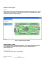
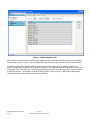
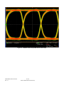
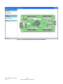
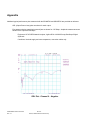
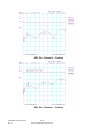
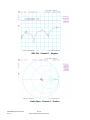
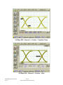
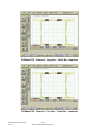
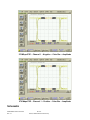
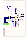
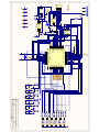
SD303EVK / SD307EVK
National Semiconductor
EVK User Manual
LMH0303 / LMH0307
Evaluation Board User Guide
February 3, 2010
Overview
The SD303/SD307 Evaluation Kit (EVK) enables evaluation of the LMH0303 3G/HD/SD SDI Cable Driver with
Cable Detect or the LMH0307 3G/HD/SD SDI Dual Cable Driver with Cable Detect. A graphical user interface
allows managing the SMBus registers of the LMH0303 or LMH0307 device.
Evaluation Kit (SD303EVK / SD307EVK) Contents
The EVK contains the following parts:
• SD303/SD307 EVK board assembly with either the LMH0303 or LMH0307 cable driver
• USB cable
• SD303/SD307 EVK User Guide
Evaluation Board Description
The evaluation board comes in two versions, depending on the cable driver installed:
1) SD303 with the LMH0303 cable driver
2) SD307 with the LMH0307 dual cable driver
The two cable drivers share the same evaluation board (SD303/SD307). The SD303/SD307 evaluation board silk
screen shows the LMH0307 pin name terminology. Table 1 shows the pin name differences between the LMH0307
¯¯¯¯ . The LMH0307 has that same output
and LMH0303. The LMH0303 has a single output channel, SDO/SDO
¯¯¯¯¯ . In addition, the LMH0307 adds a second output channel: SDO1/SDO1
¯¯¯¯¯ .
channel and refers to it as SDO0/SDO0
Table 1. LMH0307 and LMH0303 Pin Name Comparison
Reference
J3
J4
J5
J6
D9
D10
D8
D7
LMH0307 Name
SDO0
¯¯¯¯¯
SDO0
SDO1
¯¯¯¯¯
SDO1
TF0P
TF0N
TF1P
TF1N
LMH0307 Description
Channel 0 true output
Channel 0 complement output
Channel 1 true output
Channel 1 complement output
SDO0 Termination Fault
¯¯¯¯¯
SDO0 Termination Fault
SDO1 Termination Fault
¯¯¯¯¯
SDO1 Termination Fault
Figure 1 shows the SD303/SD307 evaluation board.
SD303/SD307 EVK User Guide
Rev 1.2
1 of 27
© 2010, National Semiconductor Corp.
LMH0303 Name
SDO
¯¯¯¯
SDO
LMH0303 Description
True output
Complement output
TFP
TFN
SDO Termination Fault
¯¯¯¯
SDO Termination Fault
Figure 1. SD303/SD307 Evaluation Board
SD303/SD307 EVK User Guide
Rev 1.2
2 of 27
© 2010, National Semiconductor Corp.
SDI Input and SDO Output
The SDI input connectors (J1 and J2) are 50Ω SMA connectors. The SD303/SD307 is initially configured for 100Ω
differential input. To configure the SD303/SD307 for 50Ω single-ended input, remove R28 and place 49.9Ω 0402
resistors in R9 and R10. When using only one input, the other input should be terminated with a 50Ω SMA
termination.
The SDO output connectors (J3 and J4 for the SD303; and J3, J4, J5, and J6 for the dual output SD307) are 75Ω
BNC connectors. When using only one side of an output pair, the other side should be terminated with a 75Ω BNC
termination. For example, when only using SDO0 on the LMH0307, ¯¯¯¯¯
SDO0 should be terminated with a 75Ω BNC
termination.
DC Power Connectors and USB Connector
The red and black binding posts (J8 and J9) provide power for the LMH0303/LMH0307 device, and the USB
connection provides power for the remaining board functions, including the microcontroller and the LEDs. For
proper operation, the SD303/SD307 should first be powered with a DC input voltage (between J8 and J9) of
3.3V ± 5% (3.6V maximum), and then the USB cable should be connected between the evaluation board and
the PC. The POWER LED will flash Red while the board is powered from the 3.3 VDC supply alone, and then
change to solid Green once the USB cable is connected to the PC. The POWER LED will remain Green as long as
the board is powered correctly.
JP1 – LMH0303/LMH0307 Jumper Connection to Microcontroller
A jumper block should be placed on JP1 to connect the LMH0303/LMH0307 pins to the microcontroller. The ALP
software will not function correctly if this jumper block is not in place. Separate jumpers may be used, but they
¯¯¯¯ (pins 5-6), ENABLE (pins 7-8), SDA (pins 9-10), SCL
must be placed to connect the following pins of JP1: RSTI
¯¯¯¯¯¯
¯¯¯¯¯ (pins 17-18). This jumper block (or individual
(pins 11-12), SD/HD (pins 13-14), FAULT (pins 15-16), and RSTO
jumpers) may be removed to control the LMH0303/LMH0307 pins externally, but then the microcontroller will no
longer be able to communicate with the cable driver.
Controls and Indicators
ENABLE
The ENABLE push button switch controls ENABLE, and the ENABLE LED shows its state. The ENABLE LED is
Green when the cable driver is enabled (ENABLE = 1), and Red when the cable driver is disabled (ENABLE = 0).
When the cable driver is disabled, it enters a deep power down mode, and Termination Fault detection and ¯¯¯¯
LOS
detection no longer function.
If the LOSEN register bit (bit 4 of register 05h) is set, then the cable driver can be disabled with ¯¯¯¯
LOS detection still
functioning. With LOSEN set, ¯¯¯¯
LOS is combined with the ENABLE functionality. In this mode, disabling the device
by pushing the ENABLE switch will still power down the device completely (including powering down Termination
Fault detection and ¯¯¯¯
LOS detection), but if ENABLE is left active and the signal is removed from the input, the
device will power down with the ¯¯¯¯
LOS detection still functioning. When the input signal is reapplied, the device will
power back on.
SD/HD
The SD/HD push button switch controls SD/HD, and the SD/HD LED shows its state. The SD/HD LED is Green
when the cable driver is configured for HD/3G edge rates (SD/HD = 0), and Red when the cable driver is configured
for SD edge rates (SD/HD = 1). The default setting for the SD/HD LED is Green for HD/3G edge rates.
SD303/SD307 EVK User Guide
Rev 1.2
3 of 27
© 2010, National Semiconductor Corp.
¯¯¯¯
RSTI
¯¯¯¯ push button switch controls RSTI
¯¯¯¯ , and the RSTI
¯¯¯¯ LED shows its state. RSTI
¯¯¯¯ is used to reset the cable
The RSTI
¯¯¯¯ LED is Green during normal operation (RSTI
¯¯¯¯ = 1), and Red when
driver to its default register settings. The RSTI
¯¯¯¯ = 0). To reset the device, the RSTI
¯¯¯¯ switch must be pushed twice to fully
the cable driver is held in reset (RSTI
¯¯¯¯ = 0), and again to resume normal operation (RSTI
¯¯¯¯ = 1)
toggle reset: once to put the device in reset mode (RSTI
with the default register settings.
¯¯¯¯¯
RSTO
¯¯¯¯¯ LED shows the state of RSTO
¯¯¯¯¯ . The RSTO
¯¯¯¯¯ LED is normally Red to indicate RSTO
¯¯¯¯¯ = 0. RSTO
¯¯¯¯¯ is the
The RSTO
reset output used when daisy chaining multiple cable drivers on the same SMBus. After writing a new device
¯¯¯¯¯ LED changes to Green to indicate RSTO
¯¯¯¯¯ = 1. RSTO
¯¯¯¯¯ remains
address to register 00h (the ID register), the RSTO
¯¯¯¯ .
high until the device is reset with RSTI
Termination Faults (TFxx)
The Termination Fault LEDs show the state of the Termination Faults on the cable driver outputs. The Termination
Fault LEDs are Green to indicate proper termination, Red to indicate improper or missing termination, and off to
indicate the Termination Faults are not valid under the current cable driver conditions.
The cable driver must be enabled and must have a valid input signal in order to properly detect cable termination
on the output. If no signal is detected and the ¯¯¯¯
LOS LED is Red, then the Termination Fault detectors (TF1P, TF1N,
TF0P, and TF0N for the LMH0307) cannot determine the state of the output termination and the LEDs will be off.
When a valid input signal is applied, the Termination Fault detectors will show the correct state of their termination.
If the cable driver is disabled or if the output channel is powered down, the Termination Fault LEDs will be off.
¯¯¯¯
LOS
The ¯¯¯¯
LOS LED shows the status of the input signal detector. The ¯¯¯¯
LOS LED is Green to indicate a valid input
¯¯¯¯ = 1), and Red when no signal is detected (LOS
¯¯¯¯ = 0). When the cable driver is disabled (ENABLE = 0),
signal (LOS
the ¯¯¯¯
LOS detection is disabled as well and the ¯¯¯¯
LOS LED will be Red to indicate no signal can be detected. If the
¯¯¯¯
LOS LED is Red, then the Termination Fault detection does not function and the TFxx LEDs are forced off.
With the LOSEN register bit (bit 4 of register 05h) set, the ¯¯¯¯
LOS detection may still function while the cable driver is
¯¯¯¯
disabled. In this mode, LOS is combined with the ENABLE functionality, and if the input signal is removed then the
cable driver will power down but keep the ¯¯¯¯
LOS detection running. The device will power back on once an input
signal is detected. (While in this mode, disabling the device by pushing the ENABLE switch will still power down
the device completely, including powering down Termination Fault and ¯¯¯¯
LOS detection).
LEDs and Push Button Switches Summary
Table 2 shows a summary of the LEDs provided to assist the user in determining the configuration of the board,
and Table 3 shows a summary of the push button switches provided to allow control of the board functions.
SD303/SD307 EVK User Guide
Rev 1.2
4 of 27
© 2010, National Semiconductor Corp.
Table 2. SD303/SD307 LED Indicators
LED
Reference
Default
after
Reset *
D1
POWER
Green
POWER=1, board powered
D2
ENABLE
Green
ENABLE=1, device enabled
D3
D4
D5
D6
SD/HD
MODE
RSTO
¯¯¯¯¯
RSTI
¯¯¯¯
Green
Off
Red
Green
SD/HD=0, HD/3G mode
N/A
RSTO
¯¯¯¯¯ =1
RSTI
¯¯¯¯ =1, normal operation
When flashing Red, indicates
the 3.3 VDC supply is
connected but the USB is not
ENABLE=0, device powered
down
SD/HD=1, SD mode
N/A
RSTO
¯¯¯¯¯ =0
RSTI
¯¯¯¯ =0, device held in reset
D7
TF1N
Off
TF1N=0, ¯¯¯¯¯
SDO1 properly
terminated
TF1N=1, Termination Fault on
¯¯¯¯¯
SDO1
D8
TF1P
Off
TF1P=0, SDO1 properly
terminated
TF1P=1, Termination Fault on
SDO1
D9
TF0P
Off
TF0P=0, SDO0 properly
terminated
TF0P=1, Termination Fault on
SDO0
D10
TF0N
Off
TF0N=0, ¯¯¯¯¯
SDO0 properly
terminated
TF0N=1, Termination Fault on
¯¯¯¯¯
SDO0
D11
¯¯¯¯
LOS
Red
¯¯¯¯
LOS =1, signal detected at
input
¯¯¯¯
LOS =0, no input signal
detected
Function when GREEN
Function when RED
Function when OFF
Board not powered
N/A
N/A
No function, LED always off
N/A
N/A
Termination Fault not valid
(channel is powered down or
no input signal detected)
Termination Fault not valid
(channel is powered down or
no input signal detected)
Termination Fault not valid
(channel is powered down or
no input signal detected)
Termination Fault not valid
(channel is powered down or
no input signal detected)
N/A
* Shows the default value after the board is reset (or initially powered on) with no input signal.
Table 3. SD303/SD307 Push Button Controls
Control
S1
S2
S3
Reference
SAVE
RESET
¯¯¯¯¯¯
ENABLE
S4
SD/HD
S5
S6
MODE
RSTI
¯¯¯¯
Description
No function.
Push to completely reset the board, device, and ALP software.
Toggles ENABLE. Push to set ENABLE=0 and power down the device. Push again to set ENABLE=1
and re-enable the device.
Toggles SD/HD. Push to set SD/HD=1 and enable SD mode. Push again to set SD/HD=0 and enable
HD/3G mode.
No function.
Toggles RSTI
¯¯¯¯ . Push once to set RSTI
¯¯¯¯ =0 and reset the device. Push again to set RSTI
¯¯¯¯ =1 and return
to normal operation following the reset.
SD303/SD307 EVK User Guide
Rev 1.2
5 of 27
© 2010, National Semiconductor Corp.
Software Setup
System Requirements
Operating System:
USB:
Windows XP or Vista
2.0
Installation
Download the latest software from http://www.national.com/analog/interface/sd303_307evk. Extract the
ALPF_monthdayyear_major version_minor version.exe” (ex. ALPF_07312008_125_0016.exe) file to a temporary
location that can be deleted later.
Make sure the evaluation board is not connected to the PC. The following installation instructions are for the
Windows XP Operating System.
Install the ALP software
Execute the ALP Setup Wizard program called “ALPF_monthdayyear_major version_minor version.exe” (ex.
ALPF_07312008_125_0016.exe) that was extracted to a temporary location.
There are 7 steps to the installation once the setup wizard is started:
1. Select the “Next” button.
2. Select “I accept the agreement” and then select the “Next” button.
3. Select the location to install the ALP software and then select the “Next” button.
4. Select the location for the start menu shortcut and then select the “Next” button.
5. There will then be a screen that allows the creation of a desktop and Quick Launch icon. After selecting
the desired choices select the “Next” button.
6. Select the “Install” button, and the software will then be installed to the selected location.
7. Uncheck “Launch Analog LaunchPAD” and select the “Finish” button. The ALP software will start if
“Launch Analog LaunchPAD” is checked, but it will not be useful until the USB driver is installed.
Power on the SD303/SD307 evaluation board with a 3.3 VDC power supply. Numerous LEDs will turn on, and the
POWER LED will flash Red. Connect the PC and the SD303/SD307 evaluation board together with the USB cable.
The POWER LED will stop flashing, and the “Found New Hardware Wizard” will open on the PC. Proceed to the
next section to install the USB driver.
Install the USB driver
There are 6 steps to install the USB driver:
1. Select “No, not at this time” then select the “Next” button.
2. Select “Install from a list or specific location” then select the “Next” button.
3. Select “Search for the best driver in these locations”. Uncheck “Search removable media” and check
“Include this location in the search”.
4. Browse to the Install Directory which is typically located at “C:\Program Files\National Semiconductor
Corp\Analog LaunchPAD\vx.x.x\Drivers” and select the “Next” button. Windows should find the driver.
5. Select “Continue Anyway”.
6. Select the “Finish” button.
The software installation is complete. The POWER LED on the board should turn to solid Green. The ALP
software may now be launched, as described in the next section.
SD303/SD307 EVK User Guide
Rev 1.2
6 of 27
© 2010, National Semiconductor Corp.
Software Description
Startup
Make sure all the software has been installed and the hardware is powered on and connected to the PC. Execute
“Analog LaunchPAD” from the start menu. The default start menu location is “Programs\National Semiconductor
Corp\Analog LaunchPAD vx.x.x\Analog LaunchPAD”.
The application should come up in the state shown below (for the LMH0307). If it does not, see “Trouble Shooting”
at the end of this document.
Figure 2. ALP Startup Screen for LMH0307
LMH0303/LMH0307 Profiles
There are separate profiles for the LMH0303 and the LMH0307. The ALP software automatically detects which
device is connected and configures the profile accordingly. There are four application tabs for the
LMH0303/LMH0307 device.
Information Tab
The Information tab is shown in Figure 3 (for the LMH0307).
SD303/SD307 EVK User Guide
Rev 1.2
7 of 27
© 2010, National Semiconductor Corp.
Figure 3. LMH0307 Information Tab
LMH0303 and LMH0307 Tab
The LMH0303/LMH0307 tabs present a high level view of the cable driver. Figure 4 shows this tab for the
LMH0307, and Figure 5 shows this tab for the LMH0303.
SD303/SD307 EVK User Guide
Rev 1.2
8 of 27
© 2010, National Semiconductor Corp.
Figure 4. LMH0307 Main Tab
Figure 5. LMH0303 Main Tab
SD303/SD307 EVK User Guide
Rev 1.2
9 of 27
© 2010, National Semiconductor Corp.
Firmware Version – FW Ver
FW Ver shows the version of the firmware installed on the evaluation board.
Termination Fault
These controls show the default configuration of the HD and SD Termination Fault Threshold registers and also
provide the ability to change the thresholds. The LMH0307 has two pairs of Termination Fault Threshold registers
– one HD/SD pair for each of its two output channels – as shown in Figure 4. The LMH0303 has only one HD/SD
pair of Termination Fault Threshold registers for its single output channel, as can be seen in Figure 5.
Increasing the Termination Fault Threshold settings decreases the cable driver’s sensitivity to Termination Faults.
This is useful if the cable driver is indicating termination faults when the output appears to be properly terminated.
Decreasing the Termination Fault Threshold settings increases the cable driver’s sensitivity to Termination Faults
which is useful for determining cable detection at the end of long cables.
Compare Command and Termination Fault Counters
Compare Command configures the CMPCMD section of the TEST register (08h) on the LMH0303 or LMH0307.
The Termination Fault Counters reflect the current configuration of the TEST register CMPCMD bits.
The Termination Fault Counters provide an indication of how the cable driver is reading the Termination Faults
based on the current Termination Fault Threshold settings. Perfectly terminated outputs should read back “0”, and
unterminated outputs should read back “31”.
Control
Refresh
The Refresh button provides a manual refresh of the state from the evaluation board to the LMH0303/LMH0307 tab.
Changes to the board will not be reflected in the LED icons and Line Control checkboxes on the
LMH0303/LMH0307 tab until the Refresh button is pressed. This can be done automatically by using the Auto
Refresh checkbox.
Auto Refresh Checkbox
The Auto Refresh checkbox provides an automatic refresh of the state from the evaluation board to the
LMH0303/LMH0307 tab once per second. This provides automatic updating of the LED icons and Line Control
checkboxes on the LMH0303/LMH0307 tab to reflect any board changes.
Line Control
Power Down 0 and 1 (LMH0307 only)
Power Down 0 and 1 checkboxes control the PD0 and PD1 power down bits (bits 5 and 6 in register 02h - MASK)
and will selectively power down one or both of the output channels on the LMH0307.
Enable
The Enable checkbox controls the associated ENABLE pin on the LMH0303/LMH0307. Disabling or un-checking
the Enable checkbox will force the LMH0303/LMH0307 into a deep power down mode.
RSTI
¯¯¯¯ pin. This checkbox is checked for normal operation, and un-checked to put
The RSTI checkbox controls the RSTI
the cable driver in reset.
SD303/SD307 EVK User Guide
Rev 1.2
10 of 27
© 2010, National Semiconductor Corp.
SD/HD
The SD/HD checkbox controls the state of the SD/HD pin. This checkbox is un-checked by default to enable
HD/3G mode. Enabling this checkbox sets the cable driver edge rates to SD mode.
SDO Amp
The SDO Amp controls set the amplitude of the output driver(s). The LMH0307 has two independently configurable
outputs (SDO0 and SD01) and the LMH0303 has a single configurable output (SDO). For the LMH0307,
SDO Amp 0 configures the AMP0 bits in the OUTPUT0 register (04h), and SDO Amp 1 configures the AMP1 bits in
the OUTPUT1 register (06h). For the LMH0303, SDO Amp configures the AMP bits in the OUTPUT register (04h).
The default amplitude setting is 0x10 for 800 mVP-P. The output amplitude may be lowered to around 720 mVP-P
and increased to around 880 mVP-P in roughly 5 mV increments.
LED Icons
The diagram of the LMH0303/LMH0307 device is framed by a number of colored LED icons that represent the LED
state on the board. Note that either the Refresh button or the Auto Refresh checkbox must be used to update the
LED icons in the LMH0303/LMH0307 tab to reflect any board changes.
FAULT LED
The FAULT LED shows the current state of the ¯¯¯¯¯¯
FAULT pin. The FAULT LED is Green to indicate no faults are
¯¯¯¯¯¯ = 1) and Red to indicate one or more faults have been detected (FAULT
¯¯¯¯¯¯ = 0). The Auto Refresh
detected (FAULT
checkbox should be checked in order to actively monitor the state of the ¯¯¯¯¯¯
FAULT pin.
¯¯¯¯¯¯
FAULT is triggered and set low for a Termination Fault on any output or the loss of signal on the input. ¯¯¯¯¯¯
FAULT is
cleared and set high again when the faults have been removed by either terminating the outputs, applying the input
signal, or changing the register settings in the MASK or DIRECTION registers.
Registers Tab
The Registers tab displays all registers for the LMH0303 or LMH0307. Figure 6 shows the Registers tab for the
LMH0307. The Value field indicates the value of the currently selected register.
SD303/SD307 EVK User Guide
Rev 1.2
11 of 27
© 2010, National Semiconductor Corp.
Figure 6. LMH0307 Registers Tab
Each register can be examined in detail by either double clicking on the desired registers fold bar (with the address
and the register name, e.g. 0x00 – ID) or by single clicking the icon at the right of the fold bar (two inverted carats).
The Refresh button will re-read the currently selected register and the Refresh All will read all registers in the
device. Changes may be made to the registers by checking or un-checking the individual register bits or typing in a
new register value in the Value field. After setting the appropriate register value, the Apply button must be pressed
to apply the changes. The detailed view of the STATUS register is shown in Figure 7 with Verbose Descriptions
checked and Figure 8 with Verbose Descriptions un-checked.
SD303/SD307 EVK User Guide
Rev 1.2
12 of 27
© 2010, National Semiconductor Corp.
Figure 7. LMH0307 Registers Tab with Verbose Descriptions
Figure 8. LMH0307 Registers Tab without Verbose Descriptions
The Display button provides another view of the register set and is depicted in Figure 9. The Display dialog
supports the Windows copy command (Ctrl+c).
SD303/SD307 EVK User Guide
Rev 1.2
13 of 27
© 2010, National Semiconductor Corp.
Figure 9. LMH0307 Register Display
The Load and Save buttons provide a handy mechanism for restoring or saving the register set external to the
evaluation board.
Cable Driver Output Waveform
Test Conditions
The SDO0 output of the LMH0307 on the SD307 is observed in the following example. The input signal is a 2.97
Gbps PRBS10 from the Agilent 86130A 3.6G BERT. The input signal is connected differentially to the SDI SMA
inputs on the evaluation board with matched 3’ SMA cables. The LMH0307 is running in HD/3G mode (SD/HD=0).
The SDO0 output is connected through 1m of Belden 1694A cable to the TCA75 input module on the Tektronix
DSA 71254 12.5 GHz Oscilloscope. ¯¯¯¯¯
SDO0 is terminated with a 75Ω BNC terminator.
Test Results
Figure 8 shows the typical SDO0 output waveform from the LMH0307.
SD303/SD307 EVK User Guide
Rev 1.2
14 of 27
© 2010, National Semiconductor Corp.
Figure 10. LMH0307 SDO0 Output Waveform at 2.97 Gbps
SD303/SD307 EVK User Guide
Rev 1.2
15 of 27
© 2010, National Semiconductor Corp.
Trouble Shooting
If the following window (Figure 11) opens after starting the ALP software, double check the hardware setup.
Figure 11. Analog LaunchPAD No Devices Error
It may also be that the USB driver is not installed. Check the device manager. There should be an ”NSC ALP
Nano Atmel” device under the “Universal Serial Bus Controllers” as shown below in Figure 12.
Figure 12. Windows XP, Analog LauchPAD USB Driver
SD303/SD307 EVK User Guide
Rev 1.2
16 of 27
© 2010, National Semiconductor Corp.
The software should start with only “LMH0303” or “LMH0307” in the “Devices” pull down menu. If there are more
devices then the software is most likely in demo mode. When the ALP is operating in demo mode there is a
“(Demo Mode)” indication in the lower left of the application status bar as shown in Figure 13.
Figure 13. Analog LaunchPAD in Demo Mode
Disable the demo mode by selecting the “Preferences” pull down menu and un-checking “Enable Demo Mode”.
Figure 14. Analog LaunchPAD Preferences Menu
After demo mode is disabled, the ALP software will poll the ALP hardware. The ALP software will update and have
only “LMH0303” or “LMH0307” under the “Devices” pull down menu.
SD303/SD307 EVK User Guide
Rev 1.2
17 of 27
© 2010, National Semiconductor Corp.
Figure 15. Analog LaunchPAD Screen with Demo Mode Off
SD303/SD307 EVK User Guide
Rev 1.2
18 of 27
© 2010, National Semiconductor Corp.
Bill of Materials
Reference Designator
Qty
C1, C2
C3, C4, C5, C6, C10, C11,
C14, C24, C26, C28
Description
Manufacturer
Manufacturer Part No.
2
1uF Capacitor Ceramic 10V, 20%, X5R, 0402
Panasonic
ECJ-0EB1A105M
10
4.7uF Capacitor Ceramic 6.3V, 20%, X5R, 0603
Panasonic
ECJ-1VB0J475M
C7, C25, C27, C29
4
100pF Capacitor Ceramic 50V, 5%, C0G, 0603
Panasonic
ECJ-1VC1H101J
C8, C30, C31
3
0.1uF Capacitor Ceramic 50V, 10%, X7R, 0603
Panasonic
ECJ-1VB1H104K
C9
1
Panasonic
ECJ-1VB0J106M
C12
C13, C15, C20, C21, C22,
C23
1
10uF Capacitor Ceramic 6.3V, 20%, X5R, 0603
0.033uF Capacitor Ceramic 50V, 10%, X7R,
0603
Panasonic
ECJ-1VB1H333K
6
1uF Capacitor Ceramic 16V, 10%, X5R, 0603
Panasonic
ECJ-1VB1C105K
C16, C17
2
12pF Capacitor Ceramic 50V, 5%, C0G, 0603
Panasonic
ECJ-1VC1H120J
C18, C19
D1, D2, D3, D4, D5, D6,
D7, D8, D9, D10, D11
2
220nF Capacitor Ceramic 10V, 10%, X5R, 0603
Panasonic
ECJ-1VB1A224K
11
BiColored LED (Green, Red)
LITE-ON
LTST-C155KGJRKT
D13
1
Bidrectional ESD Transient Supressor, SOT23-6
COMCHIP
CEBS0624V-G
D14
1
Diode Schottkey Array, 40V, SOT363
Diodes Inc
BAS40DW-05-7-F
J1, J2
2
SMA Connector (Edge Launch)
Johnson Components
142-0701-851
J3, J4, J5, J6
4
75 ohm BNC (Edge Launch)
Trompeter
UCBJE20-1
J7
1
USB Mini-B Recept, R/A, 5POS
Molex
54819-0572
J8
1
Binding Post (Banana Jack) Red
Emerson
111-0702-001
J9
1
Binding Post (Banana Jack) Black
Emerson
111-0703-001
JP1
1
10x2 Header, 0.100" spacing
Tyco Electronics
87215-7
JP2
1
7x2 Header, 0.100" spacing
Tyco Electronics
87215-4
L1, L2, L3, L4
4
6.8nH Inductor, 0402
Murata
LQP15MN6N8B02D
Q1
R1, R2, R3, R4, R5, R6,
R7, R8
1
MOSFET, P-Ch, 12V, 4.3A, SOT-23
International Rectifier
IRLML6401TRPBF
8
75 ohm Resistor 1%, 1/16W, 0402
ROHM
MCR01MZPF75R0
1
750 ohm Resistor 1%, 1/16W, 0402
Vishay
CRCW0402750RFKED
10
10k ohm Resistor 5%, 0.1W, 0603
ROHM
MCR03EZPJ103
10
300 ohm Resistor 5%, 0.1W, 0603
ROHM
MCR03EZPJ301
11
270 ohm Resistor 5%, 0.1W, 0603
ROHM
MCR03EZPJ271
MCR03EZPJ220
R11
R12, R13, R14, R15, R32,
R33, R34, R35, R36, R37
R16, R18, R20, R22, R24,
R40, R42, R44, R46, R48
R17, R19, R21, R23, R25,
R39, R41, R43, R45, R47,
R49
R26, R27
2
22 ohm Resistor 5%, 1/10W, 0603
ROHM
R28
1
100 ohm Resistor 1%, 1/16W, 0402
ROHM
MCR01MZPF1000
R29, R31
2
16.5k ohm Resistor 1% 0.1W, 0603
ROHM
MCR03EZPFX1652
R30
1
36.5k ohm Resistor SMD 1%, 0.1W, 0603
ROHM
MCR03EZPFX3652
R38
1
300 ohm Resistor SMD 1%, 1/16W, 0402
ROHM
MCR01MZPF3000
R50
1
52.3k ohm Resistor SMD 1%, 0.1W, 0603
ROHM
MCR03EZPFX5232
R51
1
2.74k ohm Resistor 0603 1%, 0.1W, 0603
ROHM
MCR03EZPFX2741
R52
1
100k ohm Resistor 5%, 1/10W, 0603
ROHM
MCR03EZPJ104
S1, S2, S3, S4, S5, S6
6
Switch, Tactile, SPST w/GND, SMD
Omron Electronics Inc
B3U-1100P
U1
1
AVR 8-bit Microcontroller, 128K, 64QFN
Atmel
AT90USB1287-16MU
U2
1
Regulator, LDO, 300mA, 3.3V, 8MSOP
National Semiconductor
LP3981IMM-3.3/NOPB
U3
1
LMH0307 3G SDI Dual Cable Driver, LLP16
National Semiconductor
LMH0307SQ
X1
1
Crystal, 8.00 MHz , 8 pF, Fund, SMD
NDK
NX5032GA 8MHZ AT-W
SD303/SD307 EVK User Guide
Rev 1.2
19 of 27
© 2010, National Semiconductor Corp.
Appendix
Additional typical performance plots measured with the SD303EVK and SD307EVK are provided as reference.
ORL (Output Return Loss) plots are shown for each output.
Eye patterns showing transition times and jitter are shown for 2.97 Gbps. Amplitude measurements are
shown for the outputs at 270 Mbps.
Equipment: HP 8722ES Network Analyzer, Agilent DCA-J 86100C Scope, BertScope Digital
Synthesis
Conditions: Nominal supply and room temperature, connection cables only
ORL Plot - Channel 0 – Negative
SD303/SD307 EVK User Guide
Rev 1.2
20 of 27
© 2010, National Semiconductor Corp.
ORL Plot - Channel 0 – Positive
ORL Plot - Channel 1 – Positive
SD303/SD307 EVK User Guide
Rev 1.2
21 of 27
© 2010, National Semiconductor Corp.
ORL Plot - Channel 1 – Negative
Smith Chart – Channel 0 – Positive
SD303/SD307 EVK User Guide
Rev 1.2
22 of 27
© 2010, National Semiconductor Corp.
2.97Gbps EYE - Channel 0 – Positive – Transition Times
2.97Gbps EYE - Channel 0 – Positive – Jitter
SD303/SD307 EVK User Guide
Rev 1.2
23 of 27
© 2010, National Semiconductor Corp.
270 Mbps EYE – Channel 0 – Negative – Color Bar - Amplitude
270 Mbps EYE – Channel 0 – Positive – Color Bar – Amplitude
SD303/SD307 EVK User Guide
Rev 1.2
24 of 27
© 2010, National Semiconductor Corp.
270 Mbps EYE – Channel 1 – Negative – Color Bar – Amplitude
270 Mbps EYE – Channel 1 – Positive – Color Bar – Amplitude
Schematic
SD303/SD307 EVK User Guide
Rev 1.2
25 of 27
© 2010, National Semiconductor Corp.
A
B
C
D
1
1
1
J2
VCC
J8
BANANA JACK (Red)
1
J1
GND
J9
BANANA JACK (Black)
VCC
GND
C9
10uF
2
2
GND
R9
OPEN
SDI
SDIbar
GK
RK
R10
OPEN
GND
D11
GND
GND
1
2
GA
RA
VCC
GND
C7
100pF
BiColored LED
C8
0.1uF
DVCC
VCC
GND
C1
1uF
C2
1uF
3
4
R22
300
C31
0.1uF
3
J6
L4
6.8nH
75
GND
R7
75
C6
4.7uF
SDI
SDIbar
VEE
RREF
VCC
VCC
J5
C5
4.7uF
GND
GND
GND
RTF1PLED
GND
GND
R21
270
VCC
R2
75
VCC
4
4
D8
BiColored LED
DVCC
R20
300
C30
R1
75
R15
10K
10K
R12
10K
R13
10K
R14
VCC
JP1
Header 10X2
SDA
SCL
FAULT
RSTObar
LMH0303 / LMH0307
12
11
10
9
U3
0.1uF
L3
R8
75 6.8nH
SDO1
SDO0
SDO0bar
SD/HDbar
VCC
2
1
RA
GA
RK
GK
4
3
SDO1bar
D7
BiColored LED
R23
270
75
R6
R5
GND
1
2
3
4
FAULT
DVCC
VCC
R28
100
GND
R11
VCC
RCDLED
GCDLED
750
RTF1NLED
R25
270
R24
300
3
SD/HDbar
RSTIbar
ENABLE
SDA
SCL
5
6
7
8
RSTIbar
ENABLE
GTF1PLED
GND
RSTObar
17
16
15
14
13
DAP
RSTObar
SDO1bar
SDO1
FAULT
2
4
6
8
10
12
14
16
18
20
1
3
5
7
9
11
13
15
17
19
2
1
RA
GA
4
3
RK
GK
GTF1NLED
RTF0PLED R16
300
GTF0PLED R17
270
6.8nH
L1 6.8nH
75
R3
R4
75
L2
RTF0NLED R18
300
C3
4.7uF
C4
4.7uF
RSTObar
FAULT
SD/HDbar
SCL
SDA
ENABLE
RSTIbar
GND
VCC
DVCC
GTF1NLED
RTF1NLED
GTF1PLED
RTF1PLED
GTF0NLED
RTF0NLED
GTF0PLED
RTF0PLED
GCDLED
RCDLED
4
3
4
3
LMH0303USBDigital
LMH0303USB
GTF0NLED R19
270
VCC
DVCC
GTF1NLED
RTF1NLED
GTF1PLED
RTF1PLED
GTF0NLED
RTF0NLED
GTF0PLED
RTF0PLED
GCDLED
RCDLED
GND
D9
RK
GK
RA
GA
J3
GND
J4
DVCC
2
1
2
1
GNDDVCC
RA
GA
GND
GND
BiColored LED
SDO0
SDO0bar
RK
GK
D10
BiColored LED
5
5
Title
6
6
10/7/2009
Sheet of
C:\Documents and Settings\..\LMH0303USB1.SCHDOC
Drawn By:
Number
Revision
SD303 / SD307 Evaluation Board for the LMH0303 / LMH0307
B
Size
Date:
File:
A
B
C
D
J7
FD0
GND
VBUS
Dm
Dp
ID
GND
SHLD
1
2
3
4
5
6
1
2
3
FD1
GND
1
VCC
DVCC
K1
A4
A3
FD2
16.5K 1%
1
2
3
22
22
R26
R30
36.5K 1%
D13
A
D
GNDGND
B
C
6
5
4
R27
GND
GND
Q1
C13
GND
C29
100pF
JP2
2
1
2
3
4
5
6
7
8
9 10
11 12
13 14
DVCC
GND
C12
0.033uF
GND
GND
R52
100K 5%
R51
2.74K 1%
R50
52.3K 1%
HEADER 7X2
GND
1uF
U2
8
7
6
5
IRLML6401PbF
C28
4.7uF
DVCC
LP3981
Vout NC2
Vin
Ven
NC1 Bypass
Sense GND
GND
C27
100pF
DVCC
1
2
3
4
CEBS0624V-G
C11
DVCC
C10
4.7uF
GND
DVCC
GND
4.7uF
GND
C26
4.7uF
DVCC
GND
C25
100pF
6
5
4
R29
1
GND
GND
DVCC
BAS40DW05
A1
A2
K2
D14
MINI_USB_B GND
1
C24
4.7uF
DVCC
GND
2
GND
DVCC
GND
RSTObar
FAULT
RSTIbar
C14
GND
4.7uF DVCC
1
2
3
4
5
6
7
8
9
10
11
12
13
14
15
16
PE6
PE7
UVCC
Dm
Dp
UGnd
UCap
VBUS
PE3
PB0
MCK_PB1
MOSI_PB2
MISO_PB3
PB4
PB5
PB6
3
R31
16.5K 1%
GND
C16
18pF
8MHz
X1
DVCC
GND
3
DVCC
GND
GND
SCL
SDA
A
B
C
D
1
C17
18pF
ENABLE
C15
48
47
46
45
44
43
42
41
40
39
38
37
36
35
34
33
1uF
U1
PA3
PA4
PA5
PA6
PA7
HWBz
PC7
PC6
PC5
PC4
PC3
PC2
PC1
PC0
PE1
PE0
65
GND
AT90USB1287
DAP
4
RCDLED
GCDLED
RTF0PLED
GTF0PLED
GTF0NLED
RTF0NLED
GTF1PLED
RTF1PLED
GTF1NLED
RTF1NLED
4
GND
TACTSW
3
S1
SAVE
C18 220nF
R32
10K
GND
GND
R33
10K
GND
R34
10K
GND
5
GND
DVCC
R35
10K
Date:
File:
B
Size
S4
3
GND
TACTSW
GND
R36
10K
MODE_SW
C22 1uF
S5
3
GND
TACTSW
GND
R38
300
R39
270
R40
R41
300
270
R42
R43
300
R45
270
R44
300
270
R46
R47
300
270
R48
R49
300
270
R37
10K
RSTI_SW
C23 1uF
3
S6
TACTSW
GND
4
3
4
3
4
3
4
3
4
3
4
3
6
RK
GK
D1
RA
GA
RA
GA
BiColored LED
D2
RK
GK
RK
GK
RA
GA
BiColored LED
D3
RK
GK
RA
GA
BiColored LED
D4
RK
GK
RA
GA
BiColored LED
D5
RK
GK
RA
GA
BiColored LED
D6
BiColored LED
6
2/3/2010
Sheet of
C:\Documents and Settings\..\LMH0303USB.SCHDOC
Drawn By:
Number
Revision
2
1
2
1
2
1
MODE
SD/HDbar
Enable
USB Power
A
2
1
RSTObar
DVCC
2
1
RSTIbar
D
C
B
2
1
SD303 / SD307 Evaluation Board for the LMH0303 / LMH0307
Title
TACTSW
3
S3
RESETbar ENABLE_SW SD/HDbar_SW
C19 220nF
C20 1uF
C21 1uF
S2
3
TACTSW
GND
5
2
2
1
1
2
2
1
1
2
2
1
1
2
2
1
1
2
2
1
1
2
2
1
1
SD/HDbar
64
63
62
61
60
59
58
57
56
55
54
53
52
51
50
49
AVCC
GND
AREF
PF0
PF1
PF2
PF3
PF4
PF5
PF6
PF7
GND
VCC
PA0
PA1
PA2
PB7
INT4_PE4
INT5_PE5
RESETz
VCC
GND
XTAL2
XTAL1
SCL_PD0
SDA_PD1
INT2_PD2
INT3_PD3
PD4
PD5
PD6
PD7
17
18
19
20
21
22
23
24
25
26
27
28
29
30
31
32
1
IMPORTANT NOTICE
Texas Instruments Incorporated and its subsidiaries (TI) reserve the right to make corrections, modifications, enhancements, improvements,
and other changes to its products and services at any time and to discontinue any product or service without notice. Customers should
obtain the latest relevant information before placing orders and should verify that such information is current and complete. All products are
sold subject to TI’s terms and conditions of sale supplied at the time of order acknowledgment.
TI warrants performance of its hardware products to the specifications applicable at the time of sale in accordance with TI’s standard
warranty. Testing and other quality control techniques are used to the extent TI deems necessary to support this warranty. Except where
mandated by government requirements, testing of all parameters of each product is not necessarily performed.
TI assumes no liability for applications assistance or customer product design. Customers are responsible for their products and
applications using TI components. To minimize the risks associated with customer products and applications, customers should provide
adequate design and operating safeguards.
TI does not warrant or represent that any license, either express or implied, is granted under any TI patent right, copyright, mask work right,
or other TI intellectual property right relating to any combination, machine, or process in which TI products or services are used. Information
published by TI regarding third-party products or services does not constitute a license from TI to use such products or services or a
warranty or endorsement thereof. Use of such information may require a license from a third party under the patents or other intellectual
property of the third party, or a license from TI under the patents or other intellectual property of TI.
Reproduction of TI information in TI data books or data sheets is permissible only if reproduction is without alteration and is accompanied
by all associated warranties, conditions, limitations, and notices. Reproduction of this information with alteration is an unfair and deceptive
business practice. TI is not responsible or liable for such altered documentation. Information of third parties may be subject to additional
restrictions.
Resale of TI products or services with statements different from or beyond the parameters stated by TI for that product or service voids all
express and any implied warranties for the associated TI product or service and is an unfair and deceptive business practice. TI is not
responsible or liable for any such statements.
TI products are not authorized for use in safety-critical applications (such as life support) where a failure of the TI product would reasonably
be expected to cause severe personal injury or death, unless officers of the parties have executed an agreement specifically governing
such use. Buyers represent that they have all necessary expertise in the safety and regulatory ramifications of their applications, and
acknowledge and agree that they are solely responsible for all legal, regulatory and safety-related requirements concerning their products
and any use of TI products in such safety-critical applications, notwithstanding any applications-related information or support that may be
provided by TI. Further, Buyers must fully indemnify TI and its representatives against any damages arising out of the use of TI products in
such safety-critical applications.
TI products are neither designed nor intended for use in military/aerospace applications or environments unless the TI products are
specifically designated by TI as military-grade or "enhanced plastic." Only products designated by TI as military-grade meet military
specifications. Buyers acknowledge and agree that any such use of TI products which TI has not designated as military-grade is solely at
the Buyer's risk, and that they are solely responsible for compliance with all legal and regulatory requirements in connection with such use.
TI products are neither designed nor intended for use in automotive applications or environments unless the specific TI products are
designated by TI as compliant with ISO/TS 16949 requirements. Buyers acknowledge and agree that, if they use any non-designated
products in automotive applications, TI will not be responsible for any failure to meet such requirements.
Following are URLs where you can obtain information on other Texas Instruments products and application solutions:
Products
Applications
Audio
www.ti.com/audio
Automotive and Transportation www.ti.com/automotive
Amplifiers
amplifier.ti.com
Communications and Telecom www.ti.com/communications
Data Converters
dataconverter.ti.com
Computers and Peripherals
www.ti.com/computers
DLP® Products
www.dlp.com
Consumer Electronics
www.ti.com/consumer-apps
DSP
dsp.ti.com
Energy and Lighting
www.ti.com/energy
Clocks and Timers
www.ti.com/clocks
Industrial
www.ti.com/industrial
Interface
interface.ti.com
Medical
www.ti.com/medical
Logic
logic.ti.com
Security
www.ti.com/security
Power Mgmt
power.ti.com
Space, Avionics and Defense
www.ti.com/space-avionics-defense
Microcontrollers
microcontroller.ti.com
Video and Imaging
www.ti.com/video
RFID
www.ti-rfid.com
OMAP Mobile Processors
www.ti.com/omap
Wireless Connectivity
www.ti.com/wirelessconnectivity
TI E2E Community Home Page
e2e.ti.com
Mailing Address: Texas Instruments, Post Office Box 655303, Dallas, Texas 75265
Copyright © 2012, Texas Instruments Incorporated