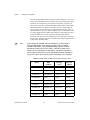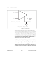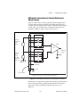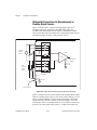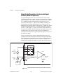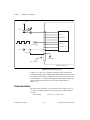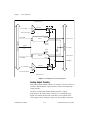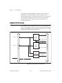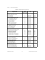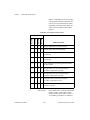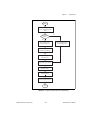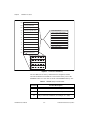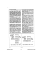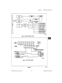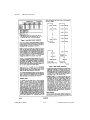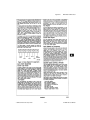
1
AT-MIO-16X
User Manual
Multifunction I/O Board for the PC AT/EISA
October 1997 Edition
Part Number 320640B-01
© Copyright 1992, 1997 National Instruments Corporation. All rights reserved.
Internet Support
[email protected]
E-mail: [email protected]
FTP Site: ftp.natinst.com
Web Address: http://www.natinst.com
Bulletin Board Support
BBS United States: (512) 794-5422
BBS United Kingdom: 01635 551422
BBS France: 01 48 65 15 59
Fax-on-Demand Support
(512) 418-1111
Telephone Support (U.S.)
Tel: (512) 795-8248
Fax: (512) 794-5678
International Offices
Australia 03 9879 5166, Austria 0662 45 79 90 0, Belgium 02 757 00 20,
Canada (Ontario) 905 785 0085, Canada (Québec) 514 694 8521, Denmark 45 76 26 00,
Finland 09 725 725 11, France 01 48 14 24 24, Germany 089 741 31 30,
Hong Kong 2645 3186, Israel 03 5734815, Italy 02 413091, Japan 03 5472 2970,
Korea 02 596 7456, Mexico 5 520 2635, Netherlands 0348 433466, Norway 32 84 84 00,
Singapore 2265886, Spain 91 640 0085, Sweden 08 730 49 70, Switzerland 056 200 51 51,
Taiwan 02 377 1200, United Kingdom 01635 523545
National Instruments Corporate Headquarters
6504 Bridge Point Parkway
Austin, TX 78730-5039
Tel: (512) 794-0100
Important Information
Warranty
The AT-MIO-16X is warranted against defects in materials and workmanship for a period of one year from the date of
shipment, as evidenced by receipts or other documentation. National Instruments will, at its option, repair or replace
equipment that proves to be defective during the warranty period. This warranty includes parts and labor.
The media on which you receive National Instruments software are warranted not to fail to execute programming
instructions, due to defects in materials and workmanship, for a period of 90 days from date of shipment, as evidenced
by receipts or other documentation. National Instruments will, at its option, repair or replace software media that do
not execute programming instructions if National Instruments receives notice of such defects during the warranty
period. National Instruments does not warrant that the operation of the software shall be uninterrupted or error free.
A Return Material Authorization (RMA) number must be obtained from the factory and clearly marked on the outside
of the package before any equipment will be accepted for warranty work. National Instruments will pay the shipping
costs of returning to the owner parts which are covered by warranty.
National Instruments believes that the information in this manual is accurate. The document has been carefully
reviewed for technical accuracy. In the event that technical or typographical errors exist, National Instruments reserves
the right to make changes to subsequent editions of this document without prior notice to holders of this edition. The
reader should consult National Instruments if errors are suspected. In no event shall National Instruments be liable for
any damages arising out of or related to this document or the information contained in it.
EXCEPT AS SPECIFIED HEREIN , NATIONAL INSTRUMENTS MAKES NO WARRANTIES, EXPRESS OR IMPLIED, AND
SPECIFICALLY DISCLAIMS ANY WARRANTY OF MERCHANTABILITY OR FITNESS FOR A PARTICULAR PURPOSE .
CUSTOMER’S RIGHT TO RECOVER DAMAGES CAUSED BY FAULT OR NEGLIGENCE ON THE PART OF N ATIONAL
INSTRUMENTS SHALL BE LIMITED TO THE AMOUNT THERETOFORE PAID BY THE CUSTOMER . NATIONAL INSTRUMENTS
WILL NOT BE LIABLE FOR DAMAGES RESULTING FROM LOSS OF DATA , PROFITS , USE OF PRODUCTS, OR INCIDENTAL OR
CONSEQUENTIAL DAMAGES , EVEN IF ADVISED OF THE POSSIBILITY THEREOF. This limitation of the liability of National
Instruments will apply regardless of the form of action, whether in contract or tort, including negligence. Any action
against National Instruments must be brought within one year after the cause of action accrues. National Instruments
shall not be liable for any delay in performance due to causes beyond its reasonable control. The warranty provided
herein does not cover damages, defects, malfunctions, or service failures caused by owner’s failure to follow the
National Instruments installation, operation, or maintenance instructions; owner’s modification of the product;
owner’s abuse, misuse, or negligent acts; and power failure or surges, fire, flood, accident, actions of third parties,
or other events outside reasonable control.
Copyright
Under the copyright laws, this publication may not be reproduced or transmitted in any form, electronic or mechanical,
including photocopying, recording, storing in an information retrieval system, or translating, in whole or in part,
without the prior written consent of National Instruments Corporation.
Trademarks
ComponentWorks™, LabVIEW™, Measure™, NI-DAQ™, RTSI™, and VirtualBench™ are trademarks of National
Instruments Corporation.
Product and company names listed are trademarks or trade names of their respective companies.
WARNING REGARDING MEDICAL AND CLINICAL USE OF NATIONAL INSTRUMENTS PRODUCTS
National Instruments products are not designed with components and testing intended to ensure a level of reliability
suitable for use in treatment and diagnosis of humans. Applications of National Instruments products involving
medical or clinical treatment can create a potential for accidental injury caused by product failure, or by errors on the
part of the user or application designer. Any use or application of National Instruments products for or involving
medical or clinical treatment must be performed by properly trained and qualified medical personnel, and all traditional
medical safeguards, equipment, and procedures that are appropriate in the particular situation to prevent serious injury
or death should always continue to be used when National Instruments products are being used. National Instruments
products are NOT intended to be a substitute for any form of established process, procedure, or equipment used to
monitor or safeguard human health and safety in medical or clinical treatment.
Table
of
Contents
About This Manual
Organization of This Manual ........................................................................................ xv
Conventions Used in This Manual................................................................................ xvi
Related Documentation................................................................................................. xvii
Customer Communication ............................................................................................ xvii
Chapter 1
Introduction
About the AT-MIO-16X ............................................................................................... 1-1
Analog Input................................................................................................... 1-2
Analog Output ................................................................................................ 1-2
Digital and Timing I/O ................................................................................... 1-3
What You Need to Get Started ..................................................................................... 1-3
Software Programming Choices ................................................................................... 1-4
National Instruments Application Software ................................................... 1-4
NI-DAQ Driver Software ............................................................................... 1-5
Register-Level Programming ......................................................................... 1-6
Optional Equipment ...................................................................................................... 1-7
Unpacking ..................................................................................................................... 1-7
Chapter 2
Configuration and Installation
Board Configuration ..................................................................................................... 2-2
AT Bus Interface ............................................................................................ 2-2
Base I/O Address Selection ............................................................................ 2-3
Interrupt and DMA Channel Selection........................................................... 2-7
Analog Input Configuration.......................................................................................... 2-7
Input Mode ..................................................................................................... 2-7
DIFF Input (Eight Channels) ........................................................... 2-8
RSE Input (16 Channels) ................................................................. 2-9
NRSE Input (16 Channels) .............................................................. 2-9
Input Polarity and Input Range....................................................................... 2-10
Considerations for Selecting Input Ranges...................................... 2-10
Analog Output Configuration ....................................................................................... 2-11
© National Instruments Corporation
v
AT-MIO-16X User Manual
Table of Contents
Analog Output Reference Selection............................................................... 2-11
Analog Output Polarity Selection .................................................................. 2-12
Digital I/O Configuration ............................................................................................. 2-12
Board and RTSI Clock Configuration.......................................................................... 2-12
Hardware Installation ................................................................................................... 2-13
Signal Connections....................................................................................................... 2-14
Signal Connection Descriptions..................................................................... 2-17
Analog Input Signal Connections .................................................................. 2-19
Types of Signal Sources................................................................................. 2-21
Floating Signal Sources ................................................................... 2-21
Ground-Referenced Signal Sources................................................. 2-21
Input Configurations ...................................................................................... 2-21
Differential Connection Considerations (DIFF Input
Configuration)............................................................................... 2-22
Differential Connections for Ground-Referenced Signal
Sources.......................................................................................... 2-23
Differential Connections for Nonreferenced or Floating
Signal Sources .............................................................................. 2-24
Single-Ended Connection Considerations ....................................... 2-26
Single-Ended Connections for Floating Signal Sources
(RSE Configuration) ..................................................................... 2-27
Single-Ended Connections for Grounded Signal Sources
(NRSE Configuration) .................................................................. 2-28
Common-Mode Signal Rejection Considerations ........................... 2-29
Analog Output Signal Connections................................................................ 2-29
Digital I/O Signal Connections ...................................................................... 2-31
Power Connections ........................................................................................ 2-32
Timing Connections for Data Acquisition and Analog Output ..................... 2-33
SCANCLK Signal ........................................................................... 2-33
EXTSTROBE* Signal ..................................................................... 2-33
EXTCONV* Signal ......................................................................... 2-34
EXTTRIG* Signal ........................................................................... 2-35
EXTGATE* Signal.......................................................................... 2-36
EXTTMRTRIG* Signal .................................................................. 2-36
Counter Signal Connections ............................................................ 2-37
Field Wiring Considerations......................................................................................... 2-42
Cabling Considerations for the AT-MIO-16X with 50-Pin I/O Connector ................. 2-43
Cabling Considerations for the AT-MIO-16X with 68-Pin I/O Connector ................. 2-44
AT-MIO-16X User Manual
vi
© National Instruments Corporation
Table of Contents
Chapter 3
Theory of Operation
Functional Overview..................................................................................................... 3-1
PC I/O Channel Interface Circuitry .............................................................................. 3-2
Analog Input and Data Acquisition Circuitry............................................................... 3-5
Analog Input Circuitry ................................................................................... 3-6
A/D Converter.................................................................................. 3-6
Analog Input Multiplexers ............................................................... 3-6
Analog Input Configuration ............................................................. 3-6
PGIA ................................................................................................ 3-7
ADC FIFO Buffer ............................................................................ 3-7
Analog Input Calibration ................................................................. 3-7
Data Acquisition Timing Circuitry................................................................. 3-8
Single-Read Timing ......................................................................... 3-8
Single-Channel Data Acquisition Timing........................................ 3-9
Multiple-Channel Data Acquisition ............................................................... 3-12
Continuous Scanning Data Acquisition Timing .............................. 3-13
Interval Scanning Data Acquisition Timing .................................... 3-14
Data Acquisition Rates..................................................................... 3-15
Analog Output and Timing Circuitry ............................................................. 3-15
Analog Output Circuitry .................................................................. 3-16
Analog Output Configuration .......................................................... 3-17
Analog Output Calibration............................................................... 3-17
DAC Waveform Circuitry and Timing........................................................... 3-18
DAC Waveform Circuitry................................................................ 3-18
DAC Waveform Timing Circuitry................................................... 3-20
FIFO Continuous Cyclic Waveform Generation ............................. 3-22
FIFO Programmed Cyclic Waveform Generation ........................... 3-23
FIFO Pulsed Waveform Generation ................................................ 3-23
Digital I/O Circuitry...................................................................................................... 3-24
Timing I/O Circuitry ..................................................................................................... 3-25
RTSI Bus Interface Circuitry ........................................................................................ 3-29
Chapter 4
Register Map and Descriptions
Register Map................................................................................................................. 4-1
Register Sizes ................................................................................................. 4-3
Register Description Format........................................................................... 4-3
Configuration and Status Register Group....................................................... 4-4
Command Register 1........................................................................ 4-5
Command Register 2........................................................................ 4-9
© National Instruments Corporation
vii
AT-MIO-16X User Manual
Table of Contents
Command Register 3 ....................................................................... 4-13
Command Register 4 ....................................................................... 4-20
Status Register 1 .............................................................................. 4-25
Status Register 2 .............................................................................. 4-30
Analog Input Register Group ......................................................................... 4-31
ADC FIFO Register......................................................................... 4-32
CONFIGMEM Register .................................................................. 4-35
Analog Output Register Group ...................................................................... 4-41
DAC0 Register ................................................................................ 4-44
DAC1 Register ................................................................................ 4-45
ADC Event Strobe Register Group ................................................................ 4-46
CONFIGMEMCLR Register........................................................... 4-47
CONFIGMEMLD Register ............................................................. 4-48
DAQ Clear Register......................................................................... 4-49
DAQ Start Register.......................................................................... 4-50
Single Conversion Register ............................................................. 4-51
ADC Calibration Register ............................................................... 4-52
DAC Event Strobe Register Group ................................................................ 4-53
TMRREQ Clear Register................................................................. 4-54
DAC Update Register ...................................................................... 4-55
DAC Clear Register......................................................................... 4-56
General Event Strobe Register Group............................................................ 4-57
DMA Channel Clear Register.......................................................... 4-58
DMATCA Clear Register ................................................................ 4-59
DMATCB Clear Register ................................................................ 4-60
External Strobe Register .................................................................. 4-61
Calibration DAC 0 Load Register ................................................... 4-62
Calibration DAC 1 Load Register ................................................... 4-63
Am9513A Counter/Timer Register Group .................................................... 4-64
Am9513A Data Register ................................................................. 4-65
Am9513A Command Register ........................................................ 4-66
Am9513A Status Register ............................................................... 4-67
Digital I/O Register Group............................................................................. 4-68
Digital Input Register ...................................................................... 4-69
Digital Output Register.................................................................... 4-70
RTSI Switch Register Group ......................................................................... 4-71
RTSI Switch Shift Register ............................................................. 4-72
RTSI Switch Strobe Register........................................................... 4-73
AT-MIO-16X User Manual
viii
© National Instruments Corporation
Table of Contents
Chapter 5
Programming
Register Programming Considerations........................................................... 5-1
Resource Allocation Considerations .............................................................. 5-1
Initializing the AT-MIO-16X ......................................................................... 5-2
Initializing the Am9513A ................................................................ 5-3
Programming the Analog Input Circuitry....................................................... 5-5
Single Conversions Using the SCONVERT or
EXTCONV* Signal ...................................................................... 5-5
Generating a Single Conversion..................................................................... 5-6
Reading a Single Conversion Result .............................................................. 5-7
Programming Single-Channel Data Acquisition Sequence............................ 5-7
Programming Data Acquisition Sequences with Channel Scanning.............. 5-10
Continuous Channel Scanning Data Acquisition............................. 5-10
Interval-Channel Scanning Data Acquisition................................................. 5-12
Data Acquisition Programming Functions ................................................................... 5-14
Clearing the Analog Input Circuitry............................................................... 5-14
Programming Single-Analog Input Channel Configurations ......................... 5-15
Programming Multiple-Analog Input Channel Configurations ..................... 5-15
Programming the Sample-Interval Counter.................................................... 5-16
Programming the Sample Counter(s) ............................................................. 5-17
Sample Counts 2 through 65,536 ..................................................... 5-18
Sample Counts Greater than 65,536 ................................................ 5-18
Programming the Scan-Interval Counter........................................................ 5-20
Applying a Trigger ......................................................................................... 5-21
Servicing the Data Acquisition Operation...................................................... 5-22
Resetting the Hardware after a Data Acquisition Operation .......................... 5-22
Resetting a Single Am9513A Counter/Timer.................................. 5-23
Programming the Analog Output Circuitry.................................................... 5-25
Cyclic Waveform Generation......................................................................... 5-26
Programmed Cycle Waveform Generation .................................................... 5-28
Pulsed Cyclic Waveform Generation ............................................................. 5-30
Waveform Generation Programming Functions ............................................ 5-32
Clearing the Analog Output Circuitry.............................................. 5-32
Selecting the Internal Update Counter ............................................. 5-32
Programming the Update-Interval Counter .................................................... 5-32
Programming the Waveform Cycle Counter.................................................. 5-34
Programming the Waveform Cycle Interval Counter .................................... 5-34
Servicing Update Requests .............................................................. 5-35
Programming the Digital I/O Circuitry......................................................................... 5-36
Programming the Am9513A Counter/Timer ................................................................ 5-37
RTSI Bus Trigger Line Programming Considerations ................................................. 5-37
© National Instruments Corporation
ix
AT-MIO-16X User Manual
Table of Contents
RTSI Switch Signal Connection Considerations.......................................................... 5-38
Programming the RTSI Switch .................................................................................... 5-39
Programming DMA Operations..................................................................... 5-41
Interrupt Programming................................................................................... 5-43
Chapter 6
Calibration Procedures
Calibration Equipment Requirements .......................................................................... 6-7
Calibration DACs ......................................................................................................... 6-8
Reference Calibration ................................................................................................... 6-8
Analog Input Calibration.............................................................................................. 6-9
Analog Output Calibration ........................................................................................... 6-10
Appendix A
Specifications
Appendix B
I/O Connector
Appendix C
AMD Am9513A Data Sheet
Appendix D
Customer Communication
Glossary
Index
Figures
Figure 1-1.
The Relationship between the Programming Environment,
NI-DAQ, and Your Hardware ............................................................... 1-6
Figure 2-1.
Figure 2-2.
Figure 2-3.
Figure 2-4.
AT-MIO-16X with 50-Pin I/O Connector Parts Locator Diagram ....... 2-1
AT-MIO-16X with 68-Pin I/O Connector Parts Locator Diagram ....... 2-2
Example Base I/O Address Switch Settings.......................................... 2-3
AT-MIO-16X 50-Pin I/O Connector..................................................... 2-15
AT-MIO-16X User Manual
x
© National Instruments Corporation
Table of Contents
Figure 2-5.
Figure 2-6.
Figure 2-7.
Figure 2-8.
Figure 2-9.
Figure 2-10.
Figure 2-11.
Figure 2-12.
Figure 2-13.
Figure 2-14.
Figure 2-15.
Figure 2-16.
Figure 2-17.
Figure 2-18.
Figure 2-19.
AT-MIO-16X 68-Pin I/O Connector ..................................................... 2-16
AT-MIO-16X PGIA .............................................................................. 2-20
Differential Input Connections for Ground-Referenced Signals ........... 2-23
Differential Input Connections for Nonreferenced Signals ................... 2-24
Single-Ended Input Connections for Nonreferenced or
Floating Signals ..................................................................................... 2-27
Single-Ended Input Connections for Ground-Referenced Signals ........ 2-28
Analog Output Connections................................................................... 2-30
Digital I/O Connections ......................................................................... 2-32
EXTSTROBE* Signal Timing .............................................................. 2-33
EXTCONV* Signal Timing .................................................................. 2-34
EXTTRIG* Signal Timing .................................................................... 2-35
EXTTMRTRIG* Signal Timing............................................................ 2-36
Event-Counting Application with External Switch Gating ................... 2-38
Frequency Measurement Application .................................................... 2-39
General-Purpose Timing Signals ........................................................... 2-41
Figure 3-1.
Figure 3-2.
Figure 3-3.
Figure 3-4.
Figure 3-5.
Figure 3-6.
Figure 3-7.
Figure 3-8.
Figure 3-9.
Figure 3-10.
Figure 3-11.
Figure 3-12.
Figure 3-13.
Figure 3-14.
Figure 3-15.
Figure 3-16.
Figure 3-17.
Figure 3-18.
Figure 3-19.
AT-MIO-16X Block Diagram ............................................................... 3-1
PC I/O Channel Interface Circuitry Block Diagram.............................. 3-3
Analog Input and Data Acquisition Circuitry Block Diagram .............. 3-5
ADC Conversion Timing....................................................................... 3-8
Single-Channel Posttrigger Data Acquisition Timing ........................... 3-10
Single-Channel Pretrigger Data Acquisition Timing............................. 3-11
Scanning Posttrigger Data Acquisition Timing ..................................... 3-13
Interval Scanning Posttrigger Data Acquisition Timing........................ 3-14
Analog Output Circuitry Block Diagram............................................... 3-16
Analog Output Waveform Circuitry ...................................................... 3-19
Posted DAC Update Timing .................................................................. 3-20
Analog Output Waveform Circuitry ...................................................... 3-21
FIFO Cyclic Waveform Generation with Disable ................................. 3-22
FIFO Programmed Cyclic Waveform Timing....................................... 3-23
FIFO Pulsed Waveform Generation Timing ......................................... 3-23
Digital I/O Circuitry Block Diagram ..................................................... 3-24
Timing I/O Circuitry Block Diagram .................................................... 3-26
Counter Block Diagram ......................................................................... 3-27
RTSI Bus Interface Circuitry Block Diagram ....................................... 3-29
Figure 5-1.
Figure 5-2.
Figure 5-3.
Figure 5-4.
Figure 5-5.
Figure 5-6.
Initializing the Am9513A Counter/Timer ............................................. 5-4
Single Conversion Programming........................................................... 5-6
Single-Channel Data Acquisition Programming ................................... 5-9
Scanning Data Acquisition Programming ............................................. 5-11
Interval Scanning Data Acquisition Programming ................................ 5-13
Resetting an Am9513A Counter/Timer ................................................. 5-24
© National Instruments Corporation
xi
AT-MIO-16X User Manual
Table of Contents
Figure 5-7.
Figure 5-8.
Figure 5-9.
Figure 5-10.
Cyclic Waveform Programming ........................................................... 5-27
Programmed Cycle Waveform Programming ....................................... 5-29
Pulsed Cyclic Waveform Programming................................................ 5-31
RTSI Switch Control Pattern................................................................. 5-40
Figure 6-1.
Figure 6-2.
Figure 6-3.
Figure 6-4.
Figure 6-5.
AT-MIO-16X EEPROM Map............................................................... 6-2
Revision and Subrevision Field............................................................. 6-5
Configuration Memory Depth Field...................................................... 6-5
ADC and DAC FIFO Depth Field......................................................... 6-6
Area Information Field .......................................................................... 6-6
Figure B-1.
Figure B-2.
AT-MIO-16X 50-Pin I/O Connector..................................................... B-2
AT-MIO-16X 68-Pin I/O Connector..................................................... B-3
Tables
Table 2-1.
Table 2-2.
Table 2-3.
Table 2-4.
Table 2-5.
Default Settings of National Instruments Products for the PC.............. 2-4
Switch Settings with Corresponding Base I/O Address and
Base I/O Address Space ........................................................................ 2-5
Available Input Configurations for the AT-MIO-16X.......................... 2-8
Actual Range and Measurement Precision Versus Input Range
Selection and Gain................................................................................. 2-11
Recommended Input Configurations for Ground-Referenced and
Floating Signal Sources......................................................................... 2-22
Table 4-1.
Table 4-2.
Table 4-3.
Table 4-4.
Table 4-5.
Table 4-6.
Table 4-7.
Table 4-8.
Table 4-9.
Table 4-10.
Table 4-11.
AT-MIO-16X Register Map.................................................................. 4-1
DMA Channel Selection ....................................................................... 4-12
DMA and Interrupt Modes .................................................................... 4-16
Interrupt Level Selection ....................................................................... 4-19
Board and RTSI Clock Selection .......................................................... 4-21
Analog Output Waveform Modes ......................................................... 4-22
Straight Binary Mode A/D Conversion Values..................................... 4-33
Two’s Complement Mode A/D Conversion Values ............................. 4-34
Input Configuration ............................................................................... 4-39
Analog Output Voltage Versus Digital Code (Unipolar Mode)............ 4-42
Analog Output Voltage Versus Digital Code (Bipolar Mode).............. 4-42
Table 5-1.
Table 5-2.
Am9513A Counter/Timer Allocations .................................................. 5-2
RTSI Switch Signal Connections .......................................................... 5-38
Table 6-1.
Table 6-2.
EEPROM Factory Area Information..................................................... 6-2
Calibration DACs .................................................................................. 6-8
AT-MIO-16X User Manual
xii
© National Instruments Corporation
Table of Contents
Table A-1.
Table A-2.
Table A-3.
Equivalent Offset Errors in 16-Bit Systems .......................................... A-3
Equivalent Gain Errors in 16-Bit Systems............................................. A-4
Typical Multiple-Channel Scanning Settling Times ............................. A-5
Table B-1.
Signal Connection Descriptions............................................................. B-4
© National Instruments Corporation
xiii
AT-MIO-16X User Manual
About
This
Manual
This manual describes the mechanical and electrical aspects of the
AT-MIO-16X board and contains information concerning its operation
and programming. The AT-MIO-16X is a high-performance,
multifunction analog, digital, and timing I/O board for the IBM PC AT
and compatibles and EISA personal computers (PCs).
Organization of This Manual
The AT-MIO-16X User Manual is organized as follows:
•
Chapter 1, Introduction, describes the AT-MIO-16X, lists the
contents of your AT-MIO-16X kit, the optional software, and
optional equipment, and explains how to unpack the AT-MIO-16X.
•
Chapter 2, Configuration and Installation, explains board
configuration, installation of the AT-MIO-16X into the PC, signal
connections to the AT-MIO-16X, and cable considerations.
•
Chapter 3, Theory of Operation, contains a functional overview of
the AT-MIO-16X and explains the operation of each functional unit
making up the AT-MIO-16X.
•
Chapter 4, Register Map and Descriptions, describes in detail the
address and function of each of the AT-MIO-16X control and status
registers.
•
Chapter 5, Programming, contains programming instructions for
operating the circuitry on the AT-MIO-16X.
•
Chapter 6, Calibration Procedures, discusses the calibration
resources and procedures for the AT-MIO-16X analog input and
analog output circuitry.
•
Appendix A, Specifications, lists the specifications of the
AT-MIO-16X.
•
Appendix B, I/O Connector, describes the pinout and signal names
for the AT-MIO-16X 50-pin I/O connector and the 68-pin I/O
connector.
© National Instruments Corporation
xv
AT-MIO-16X User Manual
About This Manual
•
Appendix C, AMD Am9513A Data Sheet, contains the
manufacturer data sheet for the AMD Am9513A System Timing
Controller integrated circuit (Advanced Micro Devices, Inc.). This
controller is used on the AT-MIO-16X.
•
Appendix D, Customer Communication, contains forms you can
use to request help from National Instruments or to comment on our
products.
•
The Glossary contains an alphabetical list and description of terms
used in this manual, including abbreviations, acronyms, metric
prefixes, mnemonics, and symbols.
•
The Index contains an alphabetical list of key terms and topics used
in this manual, including the page where you can find each one.
Conventions Used in This Manual
The following conventions are used in this manual:
<>
Angle brackets containing numbers separated by an ellipsis represent a
range of values associated with a bit or signal name (for example,
DBIO<3..0>).
This icon to the left of bold italicized text denotes a note, which alerts
you to important information.
!
This icon to the left of bold italicized text denotes a caution, which
advises you of precautions to take to avoid injury, data loss, or a
system crash.
bold italic
Bold italic text denotes a note, caution, or warning.
italic
Italic text denotes emphasis, a cross reference, or an introduction to a
key concept.
NI-DAQ
NI-DAQ is used throughout this manual to refer to the NI-DAQ
software for DOS/Windows/LabWindows unless otherwise noted.
PC
PC refers to the IBM PC AT and compatibles, and to EISA personal
computers.
The Glossary lists abbreviations, acronyms, metric prefixes,
mnemonics, symbols, and terms.
AT-MIO-16X User Manual
xvi
© National Instruments Corporation
About This Manual
Related Documentation
The following document contains information that you may find helpful
as you read this manual:
•
IBM Personal Computer AT Technical Reference
You may also want to consult the following Advanced Micro Devices
information if you plan to program the Am9513A Counter/Timer used
on the AT-MIO-16X:
•
Am9513A/Am9513 System Timing Controller
Customer Communication
National Instruments want to receive your comments on our products
and manuals. We are interested in the applications you develop with our
products, and we want to help if you have problems with them. To make
it easy for you to contact us, this manual contains comment and
configuration forms for you to complete. These forms are in
Appendix D, Customer Communication, at the end of this manual.
© National Instruments Corporation
xvii
AT-MIO-16X User Manual
Chapter
1
Introduction
This chapter describes the AT-MIO-16X, lists the contents of your
AT-MIO-16X kit, the optional software, and optional equipment, and
explains how to unpack the AT-MIO-16X.
About the AT-MIO-16X
Congratulations on your purchase of the National Instruments
AT-MIO-16X. The AT-MIO-16X is a high-performance,
software-configurable 16-bit DAQ board for laboratory, test and
measurement, and data acquisition and control applications. The
board performs high-accuracy measurements with self-calibration,
high-speed settling to 16 bits, noise as low as 0.8 LSBrms, and a
maximum DNL of ±0.5 LSB. Because of its large FIFOs and
dual-channel DMA, the AT-MIO-16X can achieve high performance,
even when used in environments that may have long interrupt latencies,
such as Windows.
Because off-the-shelf instrumentation amplifiers require 500 µsec and
more to settle to 16-bit accuracy at high gains when sampling multiple
channels, National Instruments developed the NI-PGIA. The NI-PGIA,
which is used on the AT-MIO-16X, is an instrumentation amplifier that
settles to 16 bits in 40 µs, even when the board is used at its highest gain
of 100.
A common problem with DAQ boards is that you cannot easily
synchronize several measurement functions to a common trigger or
timing event. The AT-MIO-16X has the Real-Time System Integration
(RTSI) bus to solve this problem. The RTSIbus consists of our custom
RTSI bus interface chip and a ribbon cable to route timing and trigger
signals between several functions on one or more DAQ boards in
your PC.
The AT-MIO-16X can interface to the Signal Conditioning eXtensions
for Instrumentation (SCXI) system so that you can acquire over 3,000
analog signals from thermocouples, RTDs, strain gauges, voltage
sources, and current sources. You can also acquire or generate digital
© National Instruments Corporation
1-1
AT-MIO-16X User Manual
Chapter 1
Introduction
signals for communication and control. SCXI is the instrumentation
front end for plug-in DAQ boards.
Analog Input
The AT-MIO-16X is a high-performance multifunction analog, digital,
and timing I/O board for the PC. The AT-MIO-16X has a 10 µsec,
16-bit, sampling ADC that can monitor a single input channel, or scan
through the 16 single-ended or 8 differential channels (expandable with
National Instruments multiplexing products) at a programmable gain of
1, 2, 5, 10, 20, 50, or 100 for unipolar or bipolar input ranges. A
512-word ADC FIFO buffer can perform seamless data acquisition at
the maximum rate without data loss. Internal or external triggering and
sampling are supported. If signal conditioning or additional analog
inputs are required, you can use the SCXI signal conditioning modules,
SCXI multiplexer products, or the AMUX-64T multiplexer board.
You can use the NI-DAQ software included with the AT-MIO-16X to
calibrate the analog input circuitry. This software adjusts the offset
and gain errors to zero by means of board-level calibration DACs. You
can store calibration DAC constants resulting from the calibration
procedure in the onboard EEPROM for later use. See Chapter 6,
Calibration Procedures, for additional information on calibration
procedures for the AT-MIO-16X.
Analog Output
The AT-MIO-16X also has two deglitched, double-buffered,
multiplying, 16-bit DACs that may be configured for a unipolar or
bipolar voltage output range. An onboard, +10-V reference is the
internal reference to the circuitry of the DAC. A 2,048-word DAC FIFO
buffer allows seamless waveform generation at the maximum rate
without data loss. The DAC FIFO can perform cyclic waveform
generation directly from the FIFO, independent of the PC interface.
You can use the analog output circuitry for internal timer and external
signal update capability for waveform generation.
You calibrate the analog output circuitry through the NI-DAQ software
provided with the board. This software adjusts the DAC offset and gain
errors of each channel to zero by means of board-level calibration
DACs. Calibration DAC constants resulting from the calibration
procedure may be stored in the onboard EEPROM for later use. See
Chapter 6, Calibration Procedures, for additional information on
calibration procedures for the AT-MIO-16X.
AT-MIO-16X User Manual
1-2
© National Instruments Corporation
Chapter 1
Introduction
Digital and Timing I/O
In addition to the analog input and analog output capabilities of the
AT-MIO-16X, the AT-MIO-16X also has eight digital I/O lines that
can sink up to 24 mA of current, and three independent 16-bit
counter/timers for frequency counting, event counting, and pulse
output applications. The AT-MIO-16X has timer-generated interrupts,
a high-performance RTSI bus interface, and four triggers for
system-level timing.
You can use the AT-MIO-16X, with its multifunction analog, digital,
and timing I/O, in many applications, including machine and process
control automation, level monitoring and control, instrumentation,
electronic testing, and many others. You can use the multichannel
analog input for signal and transient analysis, data logging, and
chromatography. The two analog output channels are useful for
machine and process control, analog function generation, 16-bit
resolution voltage source, and programmable signal attenuation. You
can use the eight TTL-compatible digital I/O lines for machine and
process control, intermachine communication, and relay switching
control. The three 16-bit counter/timers are useful for such functions
as pulse and clock generation, timed control of laboratory equipment,
and frequency, event, and pulse-width measurement. With all these
functions on one board, you can automatically monitor and control
laboratory processes.
The AT-MIO-16X is interfaced to the National Instruments RTSI bus.
With this bus, National Instruments AT Series boards can send timing
signals to each other. The AT-MIO-16X can send signals from the
onboard counter/timer to another board, or another board can control
single and multiple A/D conversions on the AT-MIO-16X.
Detailed specifications for the AT-MIO-16X are listed in Appendix A,
Specifications.
What You Need to Get Started
To set up and use your AT-MIO-16X Series board, you will need the
following:
❑ One of the following boards:
AT-MIO-16X 50-pin
AT-MIO-16X 68-pin
© National Instruments Corporation
1-3
AT-MIO-16X User Manual
Chapter 1
Introduction
❑ AT-MIO-16X User Manual
❑ One of the following software packages and documentation:
ComponentWorks
LabVIEW for Windows
LabWindows/CVI for Windows
Measure
NI-DAQ for PC Compatibles
VirtualBench
❑ Your computer
Software Programming Choices
You have several options to choose from when programming your
National Instruments DAQ and SCXI hardware. You can use National
Instruments application software, NI-DAQ, or register-level
programming.
National Instruments Application Software
ComponentWorks contains tools for data acquisition and instrument
control built on NI-DAQ driver software. ComponentWorks provides a
higher-level programming interface for building virtual instruments
through standard OLE controls and DLLs. With ComponentWorks, you
can use all of the configuration tools, resource management utilities,
and interactive control utilities included with NI-DAQ.
LabVIEW features interactive graphics, a state-of-the-art user
interface, and a powerful graphical programming language. The
LabVIEW Data Acquisition VI Library, a series of VIs for using
LabVIEW with National Instruments DAQ hardware, is included with
LabVIEW. The LabVIEW Data Acquisition VI Library is functionally
equivalent to NI-DAQ software.
LabWindows/CVI features interactive graphics, state-of-the-art user
interface, and uses the ANSI standard C programming language. The
LabWindows/CVI Data Acquisition Library, a series of functions for
using LabWindows/CVI with National Instruments DAQ hardware, is
included with the NI-DAQ software kit. The LabWindows/CVI Data
Acquisition Library is functionally equivalent to the NI-DAQ software.
AT-MIO-16X User Manual
1-4
© National Instruments Corporation
Chapter 1
Introduction
VirtualBench features virtual instruments that combine DAQ products,
software, and your computer to create a stand-alone instrument with the
added benefit of the processing, display, and storage capabilities of
your computer. VirtualBench instruments load and save waveform data
to disk in the same forms that can be used in popular spreadsheet
programs and word processors.
Using ComponentWorks, LabVIEW, LabWindows/CVI, or
VirtualBench software will greatly reduce the development time for
your data acquisition and control application.
NI-DAQ Driver Software
The NI-DAQ driver software is included at no charge with all National
Instruments DAQ hardware. NI-DAQ is not packaged with SCXI or
accessory products, except for the SCXI-1200. NI-DAQ has an
extensive library of functions that you can call from your application
programming environment. These functions include routines for analog
input (A/D conversion), buffered data acquisition (high-speed A/D
conversion), analog output (D/A conversion), waveform generation
(timed D/A conversion), digital I/O, counter/timer operations, SCXI,
RTSI, self-calibration, messaging, and acquiring data to extended
memory.
NI-DAQ has both high-level DAQ I/O functions for maximum ease of
use and low-level DAQ I/O functions for maximum flexibility and
performance. Examples of high-level functions are streaming data to
disk or acquiring a certain number of data points. An example of a
low-level function is writing directly to registers on the DAQ device.
NI-DAQ does not sacrifice the performance of National Instruments
DAQ devices because it lets multiple devices operate at their peak.
NI-DAQ also internally addresses many of the complex issues between
the computer and the DAQ hardware such as programming interrupts
and DMA controllers. NI-DAQ maintains a consistent software
interface among its different versions so that you can change platforms
with minimal modifications to your code. Whether you are using
conventional programming languages or National Instruments
application software, your application uses the NI-DAQ driver
software, as illustrated in Figure 1-1.
© National Instruments Corporation
1-5
AT-MIO-16X User Manual
Chapter 1
Introduction
Conventional
Programming Environment
ComponentWorks,
LabVIEW,
LabWindows/CVI, or
VirtualBench
NI-DAQ
Driver Software
DAQ or
SCXI Hardware
Personal
Computer or
Workstation
Figure 1-1. The Relationship between the Programming Environment,
NI-DAQ, and Your Hardware
Register-Level Programming
The final option for programming any National Instruments DAQ
hardware is to write register-level software. Writing register-level
programming software can be very time-consuming and inefficient,
and is not recommended for most users.
Even if you are an experienced register-level programmer, using
NI-DAQ or application software to program your National Instruments
DAQ hardware is easier than, and as flexible as, register-level
programming, and can save weeks of development time.
AT-MIO-16X User Manual
1-6
© National Instruments Corporation
Chapter 1
Introduction
Optional Equipment
National Instruments offers a variety of products to use with your
AT-MIO-16X board, including cables, connector blocks, and other
accessories, as follows:
•
Cables and cable assemblies, shielded and ribbon
•
Connector blocks, shielded and unshielded 50 and 68-pin screw
terminals
•
Real Time System Integration (RTSI) bus cables
•
SCXI modules and accessories for isolating, amplifying, exciting,
and multiplexing signals for relays and analog output. With SCXI
you can condition and acquire up to 3,072 channels.
•
Low channel count signal conditioning modules, boards, and
accessories, including conditioning for strain gauges and RTDs,
simultaneous sample and hold, and relays
For more specific information about these products, refer to your
National Instruments catalogue or call the office nearest you.
Unpacking
Your AT-MIO-16X board is shipped in an antistatic package to prevent
electrostatic damage to the board. Electrostatic discharge can damage
several components on the board. To avoid such damage in handling the
board, take the following precautions:
•
Ground yourself via a grounding strap or by holding a grounded
object.
•
Touch the antistatic package to a metal part of your computer
chassis before removing the board from the package.
•
Remove the board from the package and inspect the board for loose
components or any other sign of damage. Notify National
Instruments if the board appears damaged in any way. Do not
install a damaged board into your computer.
•
Never touch the exposed pins of connectors.
© National Instruments Corporation
1-7
AT-MIO-16X User Manual
Chapter
Configuration and
Installation
2
This chapter explains board configuration, installation of the
AT-MIO-16X into the PC, signal connections to the AT-MIO-16X,
and cable considerations.
1
4
1
3
Product Name, Assembly Number, and Revision Letter
2
Fuse
3
2
U112
4
Spare Fuse
Figure 2-1. AT-MIO-16X with 50-Pin I/O Connector Parts Locator Diagram
© National Instruments Corporation
2-1
AT-MIO-16X User Manual
Chapter 2
Configuration and Installation
1
4
1
3
Product Name, Assembly Number, and Revision Letter
2
Fuse
3
2
U112
4
Spare Fuse
Figure 2-2. AT-MIO-16X with 68-Pin I/O Connector Parts Locator Diagram
Board Configuration
The AT-MIO-16X contains one DIP switch to configure the base
address selection for the AT bus interface. The remaining resource
selections, such as DMA and interrupt channel selections, are
determined by programming the individual registers in the
AT-MIO-16X register set. The general location of the registers in the
I/O space of the PC is determined by the base address selection, whereas
the specific location of the registers within the register set is determined
by the AT-MIO-16X decode circuitry.
AT Bus Interface
Operation of the AT-MIO-16X multifunction I/O board is controlled
through accesses to registers within the board register set. Some of the
registers in the register set retain data written to them to determine
board operation. Other registers in the register set contain important
status information necessary for proper sequencing of events. Still other
registers perform functions by accessing them either by reading from or
writing to their location. However, these registers do not retain
pertinent data when written to, nor do they provide pertinent status
information when read.
AT-MIO-16X User Manual
2-2
© National Instruments Corporation
Chapter 2
Configuration and Installation
The PC defines accesses to plug-in boards to be I/O mapped accesses
within the I/O space of the computer. Locations are either written to or
read from as bytes or words. Each register in the register set is mapped
to a certain offset from the base address selection of the board as read
or write, and as a word or byte location as defined by the decode
circuitry.
Base I/O Address Selection
The AT-MIO-16X is configured at the factory to a base I/O address
of 220 hex. This base address setting is suitable for most systems.
However, if your system has other hardware at this base I/O address,
you must change either the AT-MIO-16X base address DIP switch or
the other hardware base address to avoid a conflict. Figure 2-3 shows a
graphical representation of the base address selection DIP switch, and
also shows how to reconfigure the selected base address.
3
4
5
A7
A6
A5
Switch down for 0
2
A8
Switch up for 1
1
A9
U112
O
N
O
F
F
A. Switches Set to Base I/O Address of Hex 000
3
4
5
A5
O
N
O
F
F
A7
A6
Switch down for 0
2
A8
Switch up for 1
1
A9
U112
B. Switches Set to Base I/O Address of Hex 220 (Factory Setting)
Figure 2-3. Example Base I/O Address Switch Settings
© National Instruments Corporation
2-3
AT-MIO-16X User Manual
Chapter 2
Configuration and Installation
The base address DIP switch is arranged so that a logical 1 or true state
for the associated address selection bit is selected by pushing the toggle
switch up, or toward the top of the board. Alternately, a logical 0 or
false state is selected by pushing the toggle switch down, or toward the
bottom of the board. In Figure 2-3B, A9 is up (true), A8 through A6
are low (false), and A5 is up (true). This represents a binary value of
10001XXXXX, or hex 220. The Xs indicate don’t care bits and are the
five least significant bits (LSBs) of the address (A4 through A0) used
by the AT-MIO-16X circuitry to decode the individual register
selections. The don’t care bits indicate the size of the register space. In
this case, the AT-MIO-16X uses I/O address hex 220 through hex 23F
in the factory-default setting.
Note:
If you change the AT-MIO-16X base I/O address, you must make a
corresponding change to any software packages you use with the
AT-MIO-16X. Table 2-1 lists the default settings of other National
Instruments products for the PC. Table 2-2 lists the possible switch
settings, the corresponding base I/O address, and the base I/O address
space used for that setting. For more information about the I/O address
of your PC, refer to the technical reference manual for your computer.
Table 2-1. Default Settings of National Instruments Products for the PC
Board
AT-MIO-16X User Manual
DMA
Channel
Interrupt
Level
Base I/O
Address
AT-A2150
None*
None*
120 hex
AT-AO-6/10
Channel 5
Lines 11, 12
1C0 hex
AT-DIO-32F
Channels 5, 6
Lines 11, 12
240 hex
AT-DSP2200
None*
None*
120 hex
AT-GPIB
Channel 5
Line 11
2C0 hex
AT-MIO-16
Channels 6, 7
Line 10
220 hex
AT-MIO-16D
Channels 6, 7
Lines 5, 10
220 hex
AT-MIO-16F-5
Channels 6, 7
Line 10
220 hex
AT-MIO-16X
None*
None*
220 hex
2-4
© National Instruments Corporation
Chapter 2
Configuration and Installation
Table 2-1. Default Settings of National Instruments Products for the PC (Continued)
Board
DMA
Channel
Interrupt
Level
Base I/O
Address
AT-MIO-64F-5
None*
None*
220 hex
GPIB-PCII
Channel 1
Line 7
2B8 hex
GPIB-PCIIA
Channel 1
Line 7
02E1 hex
GPIB-PCIII
Channel 1
Line 7
280 hex
Lab-PC
Channel 3
Line 5
260 hex
PC-DIO-24
None
Line 5
210 hex
PC-DIO-96
None
Line 5
180 hex
PC-LPM-16
None
Line 5
260 hex
PC-TIO-10
None
Line 5
1A0 hex
* These settings are software configurable and are disabled at startup time.
Table 2-2. Switch Settings with Corresponding Base I/O Address and
Base I/O Address Space
Switch Setting
© National Instruments Corporation
Base I/O
Address Space
Used (hex)
A9
A8
A7
A6
A5
Base I/O
Address (hex)
0
0
X
X
X
000 - E00
Reserved
0
1
0
0
0
100
100 - 11F
0
1
0
0
1
120
120 - 13F
0
1
0
1
0
140
140 - 15F
0
1
0
1
1
160
160 - 17F
0
1
1
0
0
180
180 - 19F
0
1
1
0
1
1A0
1A0 - 1BF
2-5
AT-MIO-16X User Manual
Chapter 2
Configuration and Installation
Table 2-2. Switch Settings with Corresponding Base I/O Address and
Base I/O Address Space (Continued)
Switch Setting
AT-MIO-16X User Manual
Base I/O
Address Space
Used (hex)
A9
A8
A7
A6
A5
Base I/O
Address (hex)
0
1
1
1
0
1C0
1C0 - 1DF
0
1
1
1
1
1E0
1E0 - 1FF
1
0
0
0
0
200
200 - 21F
1
0
0
0
1
220
220 - 23F
1
0
0
1
0
240
240 - 25F
1
0
0
1
1
260
260 - 27F
1
0
1
0
0
280
280 - 29F
1
0
1
0
1
2A0
2A0 - 2BF
1
0
1
1
0
2C0
2C0 - 2DF
1
0
1
1
1
2E0
2E0 - 2FF
1
1
0
0
0
300
300 - 31F
1
1
0
0
1
320
320 - 33F
1
1
0
1
0
340
340 - 35F
1
1
0
1
1
360
360 - 37F
1
1
1
0
0
380
380 - 39F
1
1
1
0
1
3A0
3A0 - 3BF
1
1
1
1
0
3C0
3C0 - 3DF
1
1
1
1
1
3E0
3E0 - 3FF
2-6
© National Instruments Corporation
Chapter 2
Configuration and Installation
Interrupt and DMA Channel Selection
The base I/O address selection is the only resource on the AT-MIO-16X
board that must be set manually before the board is placed into the PC.
The interrupt level and DMA channels used by the AT-MIO-16X are
selected via registers in the AT-MIO-16X register set. The
AT-MIO-16X powers up with all interrupt and DMA requests disabled.
To use the interrupt capability of the AT-MIO-16X, an interrupt level
must first be selected via register programming, then the specific
interrupt mode must be enabled. The same method holds for DMA
channel selection. To use the DMA capability of the board, one or two
DMA channels must be selected through the appropriate register, then
the specific DMA mode must be enabled. It is possible to have interrupt
and DMA resources concurrently enabled.
The interrupt lines supported by the AT-MIO-16X hardware are IRQ3,
IRQ4, IRQ5, IRQ7, IRQ10, IRQ11, IRQ12, and IRQ15. The DMA
channels supported are Channels 0 through 3, and Channels 5
through 7. If you use the AT-MIO-16X in an AT-type computer, you
should only use DMA Channels 5 through 7 because these are the only
16-bit channels available. If you use the board in an EISA computer, all
channels are capable of 16-bit transfers and you can use them. The
AT-MIO-16X does not use and cannot be configured to use the 8-bit
DMA Channels 0 through 3 on the PC I/O channel for 16-bit transfers.
Analog Input Configuration
The analog input section of the AT-MIO-16X is software configurable.
You can select different analog input configurations by programming
the appropriate register in the AT-MIO-16X register set. The following
paragraphs describe in detail each of the analog input categories.
Input Mode
The AT-MIO-16X offers three different input modesSE) input,
referenced single-ended (RSE) input, and differential (DIFF) input.
The single-ended input configurations use up to 16 channels. The
DIFF input configuration uses up to eight channels. Input modes are
programmed on a per channel basis for multimode scanning. For
example, the circuitry can be configured to effectively scan
12 channels, four differentially configured channels and eight
single-ended channels. The input configurations are described in
Table 2-3.
© National Instruments Corporation
2-7
AT-MIO-16X User Manual
Chapter 2
Configuration and Installation
Table 2-3. Available Input Configurations for the AT-MIO-16X
Configuration
Description
DIFF
Differential configurationnput of the PGIA tied to
the multiplexer output of Channels 8 through 15.
RSE
Referenced single-ended configurationve (–) input
of the PGIA referenced to analog ground.
NRSE
Nonreferenced single-ended configurationative (–)
input of the PGIA tied to AI SENSE and not
connected to ground.
While reading the following paragraphs, you may find it helpful to refer
to the Analog Input Signal Connections section later in this chapter,
which contains diagrams showing the signal paths for the three
configurations.
DIFF Input (Eight Channels)
DIFF input means that each input signal has its own reference, and the
difference between each signal and its reference is measured. The signal
and its reference are assigned an input channel. This is the
recommended configuration. With this input configuration, the
AT-MIO-16X can monitor up to eight different analog input signals.
This configuration is selected via software. See the configuration
memory register and Table 4-9 in Chapter 4, Register Map and
Descriptions. The results of this configuration are as follows:
•
One of Channels 0 through 7 is tied to the positive (+) input of
the PGIA.
•
One of Channels 8 through 15 is tied to the negative (–) input of
the PGIA.
•
Multiplexer control is configured to control up to eight input
channels.
•
AI SENSE may be driven by the board analog input ground or left
unconnected.
Considerations for using the DIFF input configuration are discussed in
the Signal Connections section later in this chapter. Figure 2-8 shows a
schematic diagram of this configuration.
AT-MIO-16X User Manual
2-8
© National Instruments Corporation
Chapter 2
Configuration and Installation
RSE Input (16 Channels)
RSE input means that all input signals are referenced to a common
ground point that is also tied to the analog input ground of the
AT-MIO-16X board. The negative (–) input of the differential input
amplifier is tied to the analog ground. This configuration is useful when
measuring floating signal sources. See the Types of Signal Sources
section later in this chapter for more information. With this input
configuration, the AT-MIO-16X can monitor up to 16 different analog
input signals. This configuration is selected via software. See the
configuration memory register and Table 4-9 in Chapter 4, Register
Map and Descriptions. The results of this configuration are as follows:
•
The negative (–) input of the PGIA is tied to the PGIA signal
ground.
•
Multiplexer outputs are tied together into the positive (+) input
of the PGIA.
•
Multiplexer control is configured to control up to 16 input
channels.
•
AI SENSE may be driven by the board analog input ground or
left unconnected.
Considerations for using the RSE configuration are discussed in the
Signal Connections section later in this chapter. Figure 2-18 shows
a schematic diagram of this configuration.
NRSE Input (16 Channels)
NRSE input means that all input signals are referenced to the same
common-mode voltage, but this common-mode voltage can float
with respect to the analog ground of the AT-MIO-16X board. This
common-mode voltage is subsequently subtracted from the signals
by the input PGIA. This configuration is useful when measuring
ground-referenced signal sources. See the Types of Signal Sources
section later in this chapter for more information. With this input
configuration, the AT-MIO-16X can measure up to 16 different analog
input signals. This configuration is selected via software. See the
configuration memory register and Table 4-9 in Chapter 4, Register
Map and Descriptions, for additional information. The results of this
configuration are as follows:
•
AI SENSE is tied into the negative (–) input of the PGIA.
•
Multiplexer outputs are tied together into the positive (+) input
of the PGIA.
© National Instruments Corporation
2-9
AT-MIO-16X User Manual
Chapter 2
Configuration and Installation
•
Note:
Multiplexer control is configured to control up to 16 input
channels.
The NRSE input mode is the only mode in which the AI SENSE signal
from the I/O connector is used as an input. In all other modes, AI SENSE
is either programmed to be unused or driven with the board analog input
ground.
Considerations for using the NRSE input configuration are discussed in
the Signal Connections section later in this chapter. Figure 2-8 shows a
schematic diagram of this configuration.
Input Polarity and Input Range
The AT-MIO-16X has two polarities: unipolar input and bipolar input.
Unipolar input means that the input voltage range is between 0 and Vref
where Vref is a positive reference voltage. Bipolar input means that the
input voltage range is between –V ref and +Vref. The AT-MIO-16X has
a maximum unipolar input range of 10 V, and a maximum bipolar input
range of 20 V (±10 V). Polarity and range settings are programmed on
a per channel basis through the configuration memory register.
Considerations for Selecting Input Ranges
Input polarity and range selection depend on the expected input range
of the incoming signal. A large input range can accommodate a large
signal variation but lowers the voltage resolution. Choosing a smaller
input range increases the voltage resolution but may result in the input
signal going out of range. For best results, the input range should be
matched as closely as possible to the expected range of the input signal.
For example, if the input signal is certain not to be negative (below
0 V), a unipolar input is best. However, if the signal is ever negative,
inaccurate readings will occur if unipolar input polarity is used.
The software-programmable gain on the AT-MIO-16X increases its
overall flexibility by matching the input signal ranges to those that the
AT-MIO-16X analog-to-digital converter (ADC) can accommodate.
The AT-MIO-16X board has gains of 1, 2, 5, 10, 20, 50, and 100 and is
suited for a wide variety of signal levels. With the proper gain setting,
the full resolution of the ADC can be used to measure the input signal.
Table 2-4 shows the overall input range and precision according to the
input range configuration and gain used.
AT-MIO-16X User Manual
2-10
© National Instruments Corporation
Chapter 2
Configuration and Installation
Table 2-4. Actual Range and Measurement Precision Versus Input Range
Selection and Gain
Range
Configuration
Gain
Actual
Input Range
Precision*
0 to +10 V
1.0
2.0
5.0
10.0
20.0
50.0
100.0
0 to +10.0 V
0 to +5.0 V
0 to +2.0 V
0 to +1.0 V
0 to +0.5 V
0 to +0.2 V
0 to 100.0 mV
152.59 µV
76.29 µV
30.52 µV
15.26 µV
7.63 µV
3.05 µV
1.53 µV
–10 to +10 V
1.0
2.0
5.0
10.0
20.0
50.0
100.0
–10.0 to +10.0 V
–5.0 to +5.0 V
–2.0 to +2.0 V
–1.0 to +1.0 V
–0.5 to +0.5 V
–0.2 to +0.2 V
–100.0 to +100.0 mV
305.18 µV
152.59 µV
61.04 µV
30.52 µV
15.26 µV
6.10 µV
3.05 µV
* The value of 1 LSB of the 16-bit ADC; that is, the voltage increment corresponding to
a change of 1 count in the ADC 16-bit count.
Note: See Appendix A, Specifications, for absolute maximum ratings.
Analog Output Configuration
The AT-MIO-16X supplies two channels of analog output voltage at
the I/O connector. The analog output circuitry is configurable through
programming of a register in the board register set. The reference and
range for the analog output circuitry can be selected through software.
The reference can be either internal or external, whereas the range can
be either bipolar or unipolar.
Analog Output Reference Selection
Each DAC can be connected to the AT-MIO-16X internal reference of
10 V or to the external reference signal connected to the EXTREF pin
on the I/O connector. This signal applied to EXTREF must be between
–18 and +18 V. Both channels need not be configured for the same
mode.
© National Instruments Corporation
2-11
AT-MIO-16X User Manual
Chapter 2
Configuration and Installation
Analog Output Polarity Selection
Each analog output channel can be configured for either unipolar or
bipolar output. A unipolar configuration has a range of 0 to V ref at the
analog output. A bipolar configuration has a range of –V ref to +Vref at
the analog output. V ref is the voltage reference used by the DACs in the
analog output circuitry and can be either the 10-V onboard reference or
an externally supplied reference between –18 and +18 V. Both channels
need not be configured for the same range.
Selecting a bipolar range for a particular DAC means that any data
written to that DAC will be interpreted as two’s complement format.
In two’s complement mode, data values written to the analog output
channel range from –32,768 to +32,767 decimal (8000 to 7FFF hex). If
unipolar range is selected, data is interpreted in straight binary format.
In straight binary mode, data values written to the analog output channel
range from 0 to 65,535 decimal (0 to FFFF hex).
Digital I/O Configuration
The AT-MIO-16X contains eight lines of digital I/O for
general-purpose use. The eight digital I/O lines supplied are configured
as two 4-bit ports. Each port can be individually configured through
programming of a register in the board register set as either input or
output. At system startup and reset, the digital I/O ports are both
configured for input.
Board and RTSI Clock Configuration
When multiple AT Series boards are connected via the RTSI bus,
you may want all of the boards to use the same 10-MHz clock. This
arrangement is useful for applications that require counter/timer
synchronization between boards. Each AT Series board with a RTSI bus
interface has an onboard 10-MHz oscillator. Thus, one board can drive
the RTSI bus clock signal, and the other boards can receive this signal
or disconnect from it.
Many functions performed by the AT-MIO-16X board require a
frequency timebase to generate the necessary timing signals for
controlling ADC conversions, DAC updates, or general-purpose signals
at the I/O connector. You select this timebase through programming one
of the registers in the AT-MIO-16X register set.
AT-MIO-16X User Manual
2-12
© National Instruments Corporation
Chapter 2
Configuration and Installation
The AT-MIO-16X can use either its internal 10-MHz timebase, or it can
use a timebase received over the RTSI bus. In addition, if the board is
configured to use the internal timebase, it can also be programmed to
drive its internal timebase over the RTSI bus to another board that is
programmed to receive this timebase signal. This clock source, whether
local or from the RTSI bus, is then divided by 10 and used as the
Am9513A frequency source. The default configuration at startup is to
use the internal timebase without driving the RTSI bus timebase signal.
Hardware Installation
You can install the AT-MIO-16X in any available 16-bit expansion
slot in your AT Series computer. However, to achieve best noise
performance, you should leave as much room as possible between the
AT-MIO-16X and other boards and hardware. The AT-MIO-16X does
not work if installed in an 8-bit expansion slot (PC Series). After you
have made any necessary changes, verified, and recorded the switches
and jumper settings (a form is included for this purpose in Appendix D,
Customer Communication), you are ready to install the AT-MIO-16X.
The following are general installation instructions, but consult your PC
user manual or technical reference manual for specific instructions and
warnings.
1.
Turn off your computer.
2.
Remove the top cover or access port to the I/O channel.
3.
Remove the expansion slot cover on the back panel of the
computer.
4.
Insert the AT-MIO-16X into a 16-bit slot. Do not force the board
into place. Verify that there are no extended components on the
circuit board of the computer that may touch or be in the way of
any part of the AT-MIO-16X.
5.
Attach a RTSI cable to the RTSI connectors to connect AT Series
boards to each other.
6.
Screw the AT-MIO-16X mounting bracket to the back panel rail
of the computer.
7.
Check the installation.
8.
Replace the cover.
The AT-MIO-16X board is installed and ready for operation.
© National Instruments Corporation
2-13
AT-MIO-16X User Manual
Chapter 2
Configuration and Installation
Signal Connections
This section describes input and output signal connections to the
AT-MIO-16X board via the AT-MIO-16X I/O connector. This section
also includes specifications and connection instructions for the signals
given on the AT-MIO-16X I/O connector.
Caution:
AT-MIO-16X User Manual
Connections that exceed any of the maximum ratings of input or output
signals on the AT-MIO-16X can result in damage to the AT-MIO-16X
board and to the PC. Maximum input ratings for each signal are given in
this chapter under the discussion of that signal. National Instruments is
not liable for any damages resulting from such signal connections.
2-14
© National Instruments Corporation
Chapter 2
Configuration and Installation
Figure 2-4 shows the pin assignments for the AT-MIO-16X 50-pin I/O
connector.
AI GND
1
2
AI GND
ACH0
3
4
ACH8
ACH1
5
6
ACH9
ACH2
7
8
ACH3
9 10
ACH10
ACH11
ACH4
11 12
ACH12
ACH5
13 14
ACH13
ACH6
ACH7
AI SENSE
15 16
ACH14
17 18
ACH15
19 20
DAC0 OUT
DAC1 OUT
AO GND
21 22
23 24
EXTREF
DIG GND
ADIO0
25 26
BDIO0
ADIO1
27 28
ADIO2
29 30
BDIO1
BDIO2
ADIO3
31 32
DIG GND
33 34
BDIO3
+5 V
+5 V
EXTSTROBE*
35 36
SCANCLK
37 38
EXTTRIG*
EXTGATE*
39 40
SOURCE1
OUT1
41 42
EXTCONV*
GATE1
43 44
EXTTMRTRIG*
GATE2
SOURCE5
45 46
OUT2
47 48
49 50
GATE5
OUT5
FOUT
Figure 2-4. AT-MIO-16X 50-Pin I/O Connector
© National Instruments Corporation
2-15
AT-MIO-16X User Manual
Chapter 2
Configuration and Installation
Figure 2-5 shows the pin assignments for the AT-MIO-16X 68-pin I/O
connector.
ACH8
34 68
ACH1
33 67
AIGND
AIGND
32 66
ACH9
ACH10
31 65
ACH2
ACH3
30 64
AIGND
AIGND
29 63
ACH11
ACH4
28 62
AISENSE
AIGND
27 61
ACH12
ACH13
26 60
ACH5
ACH6
25 59
AIGND
AIGND
24 58
ACH14
ACH15
23 57
ACH7
DAC0
22 56
AIGND
AOGND
ACH0
DAC1
21 55
EXTREF
20 54
AOGND
BDIO0
19 53
DGND
DGND
18 52
ADIO0
ADIO1
17 51
BDIO1
BDIO2
16 50
DGND
15 49
DGND
ADIO2
+5 V
14 48
BDIO3
DGND
ADIO3
DGND
13 47
12 46
EXTTRIG*
11 45
EXTSTROBE*
EXTGATE*
10 44
DGND
DGND
+5 V
9 43
EXTCONV*
8 42
SOURCE1
GATE1
SCANCLK
DGND
7 41
EXTTMRTRIG*
6 40
OUT1
GATE2
5 39
DGND
DGND
4 38
OUT2
GATE5
3 37
SOURCE5
OUT5
2 36
DGND
FOUT
1 35
DGND
Figure 2-5. AT-MIO-16X 68-Pin I/O Connector
AT-MIO-16X User Manual
2-16
© National Instruments Corporation
Chapter 2
Configuration and Installation
Signal Connection Descriptions
Signal Names
Reference
Descriptions
AI GND
N/A
Analog Input Ground—These pins are the reference point for
single-ended measurements and the bias current return point
for differential measurements.
ACH<0..15>
AI GND
Analog Input Channels 0 through 15—In differential mode,
the input is configured for up to eight channels. In
single-ended mode, the input is configured for up to
16 channels.
AI SENSE
AI GND
Analog Input Sense—This pin serves as the reference node
when the board is in NRSE configuration. If desired, this
signal can be programmed to be driven by the board analog
input ground in the DIFF and RSE analog input modes.
DAC0 OUT
AO GND
Analog Channel 0 Output—This pin supplies the voltage
output of analog output Channel 0.
DAC1 OUT
AO GND
Analog Channel 1 Output—This pin supplies the voltage
output of analog output Channel 1.
EXTREF
AO GND
External Reference—This is the external reference input for
the analog output circuitry.
AO GND
N/A
Analog Output Ground—The analog output voltages are
referenced to this node.
DIG GND
N/A
Digital Ground—This pin supplies the reference for the
digital signals at the I/O connector as well as the +5 VDC
supply.
ADIO<0..3>
DIG GND
Digital I/O port A signals.
BDIO<0..3>
DIG GND
Digital I/O port B signals.
+5 V
DIG GND
+5 VDC Source—These pins are fused for up to 1 A of +5 V
supply.
© National Instruments Corporation
2-17
AT-MIO-16X User Manual
Chapter 2
Configuration and Installation
Signal Names
Reference
Descriptions
SCANCLK
DIG GND
Scan Clock—This pin pulses once for each A/D conversion in
the scanning modes. The low-to-high edge indicates when the
input signal can be removed from the input or switched to
another signal.
EXTSTROBE*
DIG GND
External Strobe—Writing to the EXTSTROBE Register
results in a minimum 500-nsec low pulse on this pin.
EXTTRIG*
DIG GND
External Trigger—In posttrigger data acquisition sequences, a
high-to-low edge on EXTTRIG* initiates the sequence. In
pretrigger applications, the first high-to-low edge of
EXTTRIG* initiates pretrigger conversions while the second
high-to-low edge initiates the posttrigger sequence.
EXTGATE*
DIG GND
External Gate—When EXTGATE* is low, A/D conversions
are inhibited. When EXTGATE* is high, A/D conversions are
enabled.
EXTCONV*
DIG GND
External Convert—A high-to-low edge on EXTCONV*
causes an A/D conversion to occur. Conversions initiated by
the EXTCONV* signal are inhibited outside of a data
acquisition sequence, and when gated off.
SOURCE1
DIG GND
SOURCE1—This pin is from the Am9513A Counter 1 signal.
GATE1
DIG GND
GATE1—This pin is from the Am9513A Counter 1 signal.
OUT1
DIG GND
OUTPUT1—This pin is from the Am9513A Counter 1 signal.
EXTTMRTRIG*
DIG GND
External Timer Trigger—If selected, a high-to-low edge on
EXTTMRTRIG* results in the output DACs being updated
with the value written to them in the posted update mode.
EXTTMRTRIG* will also generate a timed interrupt if
enabled.
GATE2
DIG GND
GATE2—This pin is from the Am9513A Counter 2 signal.
OUT2
DIG GND
OUTPUT2—This pin is from the Am9513A Counter 2 signal.
SOURCE5
DIG GND
SOURCE5—This pin is from the Am9513A Counter 5 signal.
GATE5
DIG GND
GATE5—This pin is from the Am9513A Counter 5 signal.
AT-MIO-16X User Manual
2-18
© National Instruments Corporation
Chapter 2
Signal Names
Reference
Configuration and Installation
Descriptions
OUT5
DIG GND
OUT5—This pin is from the Am9513A Counter 5 signal.
FOUT
DIG GND
Frequency Output—This pin is from the Am9513A FOUT
signal.
The signals on the connector can be classified as analog input signals,
analog output signals, digital I/O signals, digital power connections, or
timing I/O signals. Signal connection guidelines for each of these
groups are given in the following section.
Analog Input Signal Connections
AI GND is an analog input common signal that is routed directly to
the ground tie point on the AT-MIO-16X. These pins can be used for a
general analog power ground tie point to the AT-MIO-16X if necessary.
In NRSE mode, AI SENSE is connected internally to the negative (–)
input of the AT-MIO-16X PGIA. In the DIFF and RSE modes, this
signal is driven by AI GND or left unconnected.
Signal pins ACH<0..15> are tied to the 16 analog input channels of
the AT-MIO-16X. In single-ended mode, signals connected to
ACH<0..15> are routed to the positive (+) input of the AT-MIO-16X
PGIA. In differential mode, signals connected to ACH<0..7> are routed
to the positive (+) input of the AT-MIO-16X PGIA, and signals
connected to ACH<8..15> are routed to the negative (–) input of the
AT-MIO-16X PGIA.
Caution:
Exceeding the differential and common-mode input ranges results in
distorted input signals. Exceeding the maximum input voltage rating can
result in damage to the AT-MIO-16X board and to the PC. National
Instruments is not liable for any damages resulting from such signal
connections.
Connection of analog input signals to the AT-MIO-16X depends on the
configuration of the AT-MIO-16X analog input circuitry and the type
of input signal source. With the different AT-MIO-16X configurations,
you can use the AT-MIO-16X PGIA in different ways. Figure 2-6
shows a diagram of the AT-MIO-16X PGIA.
© National Instruments Corporation
2-19
AT-MIO-16X User Manual
Chapter 2
Configuration and Installation
Programmable Gain
V in+
+
+
Gain
V in-
-
Vm Measured
Voltage
-
Gain = 1, 2, 5, 10, 20, 50, 100
V m = [ V in+
- V in - ] * GAIN
Figure 2-6. AT-MIO-16X PGIA
The AT-MIO-16X PGIA applies gain and common-mode voltage
rejection, and presents high-input impedance to the analog input signals
connected to the AT-MIO-16X board. Signals are routed to the positive
(+) and negative (–) inputs of the PGIA through input multiplexers on
the AT-MIO-16X. The PGIA converts two input signals to a signal that
is the difference between the two input signals multiplied by the gain
setting of the amplifier. The amplifier output voltage is referenced to
the AT-MIO-16X ground. The AT-MIO-16X ADC measures this
output voltage when it performs A/D conversions.
All signals must be referenced to ground, either at the source device or
at the AT-MIO-16X. If you have a floating source, the AT-MIO-16X
should reference the signal to ground by using the RSE input mode or
the DIFF input configuration with bias resistors (see the Differential
Connections for Nonreferenced or Floating Signal Sources section later
in this chapter). If you have a grounded source, the AT-MIO-16X
should not reference the signal to AI GND. The AT-MIO-16X board
avoids this reference by using the DIFF or NRSE input configurations.
AT-MIO-16X User Manual
2-20
© National Instruments Corporation
Chapter 2
Configuration and Installation
Types of Signal Sources
When configuring the input mode of the AT-MIO-16X and making
signal connections, you must first determine whether the signal source
is floating or ground-referenced. These two types of signals are
described in the following sections.
Floating Signal Sources
A floating signal source is one that is not connected in any way to the
building ground system but rather has an isolated ground reference
point. Some examples of floating signal sources are outputs of
transformers, thermocouples, battery-powered devices, optical isolator
outputs, and isolation amplifiers. An instrument or device that provides
an isolated output falls into the floating signal source category. The
ground reference of a floating signal must be tied to the AT-MIO-16X
analog input ground in order to establish a local or onboard reference
for the signal. Otherwise, the measured input signal varies as the source
floats out of the common-mode input range.
Ground-Referenced Signal Sources
A ground-referenced signal source is one that is connected in some way
to the building system ground and is therefore already connected to a
common ground point with respect to the AT-MIO-16X board,
assuming that the PC AT is plugged into the same power system.
Nonisolated outputs of instruments and devices that plug into the
building power system fall into this category.
The difference in ground potential between two instruments connected
to the same building power system is typically between 1 mV and
100 mV but can be much higher if power distribution circuits are not
properly connected. If grounded signal source is improperly measured,
this difference may show up as an error in the measurement. The
following connection instructions for grounded signal sources are
designed to eliminate this ground potential difference from the
measured signal.
Input Configurations
The AT-MIO-16X can be configured for one of three input modes:
NRSE, RSE, or DIFF. The following sections discuss the use of
single-ended and differential measurements, and considerations for
measuring both floating and ground-referenced signal sources.
© National Instruments Corporation
2-21
AT-MIO-16X User Manual
Chapter 2
Configuration and Installation
Table 2-5 summarizes the recommended input configuration for both
types of signal sources.
Table 2-5. Recommended Input Configurations for Ground-Referenced and
Floating Signal Sources
Type of Signal
Recommended Input
Configuration
Ground-referenced (nonisolated outputs,
plug-in instruments)
DIFF
NRSE
Floating (batteries, thermocouples, isolated
outputs)
DIFF with bias resistors
RSE
Differential Connection Considerations
(DIFF Input Configuration)
Differential connections are those in which each AT-MIO-16X analog
input signal has its own reference signal or signal return path. These
connections are available when the AT-MIO-16X is configured in the
DIFF input mode. Each input signal is tied to the positive (+) input of
the PGIA; and its reference signal, or return, is tied to the negative (–)
input of the PGIA.
When the AT-MIO-16X is configured for differential input, each signal
uses two multiplexer inputs—one for the signal and one for its reference
signal. Therefore, with a differential configuration, up to eight analog
input channels are available. Differential input connections should be
used when any of the following conditions are present:
•
You are connecting eight or fewer signals to the AT-MIO-16X.
•
Input signals are low level (less than 1 V).
•
Leads connecting the signals to the AT-MIO-16X are greater than
10 ft.
•
Any of the input signals require a separate ground-reference point
or return signal.
•
The signal leads travel through noisy environments.
Differential signal connections reduce picked-up noise and increase
common-mode noise rejection. Differential signal connections also
permit input signals to float within the common-mode limits of the
PGIA.
AT-MIO-16X User Manual
2-22
© National Instruments Corporation
Chapter 2
Configuration and Installation
Differential Connections for Ground-Referenced
Signal Sources
Figure 2-7 shows how to connect a ground-referenced signal source
to an AT-MIO-16X board configured in the DIFF input mode. The
AT-MIO-16X analog input circuitry must be configured for DIFF input
to make these types of connections. Configuration instructions are
included in Chapter 4, Register Map and Descriptions.
ACH<0..7>
GroundReferenced
Signal
Source
+
V
s
PGIA
+
-
Gain
ACH<8..15>
CommonMode
Noise,
Ground
Potential,
and so on
V
m
+
Measured
Voltage
-
+
V
cm
-
Input Multiplexers
AI SENSE
AI GND
I/O Connector
AT-MIO-16X Board in the DIFF Input Configuration
Figure 2-7. Differential Input Connections for Ground-Referenced Signals
With this type of connection, the PGIA rejects both the common-mode
noise in the signal and the ground potential difference between the
signal source and the AT-MIO-16X ground, shown as Vcm in
Figure 2-7.
© National Instruments Corporation
2-23
AT-MIO-16X User Manual
Chapter 2
Configuration and Installation
Differential Connections for Nonreferenced or
Floating Signal Sources
Figure 2-8 shows how to connect a floating signal source to an
AT-MIO-16X board configured in the DIFF input mode. The
AT-MIO-16X analog input circuitry must be configured for DIFF
input to make these types of connections. Configuration instructions are
included in Chapter 4, Register Map and Descriptions.
ACH<0..7>
Bias
Resistors
Floating
Signal
Source
+
V
s
PGIA
+
-
Gain
ACH<8..15>
-
V
m
+
Measured
Voltage
-
Bias
Current
Return
Paths
Input Multiplexers
AI SENSE
AI GND
I/O Connector
AT-MIO-16X Board in the DIFF Input Configuration
Figure 2-8. Differential Input Connections for Nonreferenced Signals
Figure 2-8 shows two bias resistors connected in parallel with the signal
leads of a floating signal source. If the source is truly floating, it is not
likely to remain within the common-mode signal range of the PGIA,
and the PGIA will saturate (causing erroneous readings). You must
reference the source to AI GND. The best way is simply to connect the
positive side of the signal to the positive (+) input of the PGIA and
AT-MIO-16X User Manual
2-24
© National Instruments Corporation
Chapter 2
Configuration and Installation
connect the negative side of the signal to AI GND as well as to the
negative (–) input of the PGIA. This works well for DC-coupled sources
with low source impedance (less than 100 Ω). However, for larger
source impedances, this connection leaves the differential signal path
significantly out of balance. Noise that couples electrostatically onto
the positive (+) line does not couple onto the negative (–) line because
it is connected to ground. Hence, this noise appears as a
differential-mode signal instead of a common-mode signal, and so the
PGIA does not reject it. In this case, instead of directly connecting the
negative (–) line to AI GND, connect it to AI GND through a resistor
that is about 100 times the equivalent source impedance. This puts the
signal path nearly in balance, so about the same noise couples onto both
(+) and (–) connections, yielding better rejection of electrostatically
coupled noise. Also, this configuration does not load down the source
(other than the 100-GΩ input impedance of the PGIA). You can fully
balance the signal path by connecting another resistor of the same value
between the positive (+) input and AI GND. This fully balanced
configuration offers slightly better noise rejection, but has the
disadvantage of loading the source down with the series combination
(sum) of the two resistors. If, for instance, the source impedance is 2 kΩ
and the two resistors are each 100 kΩ, the resistors load down the
source with 200 kΩ and produce a –1% gain error.
Both inputs of the PGIA require a DC path to ground in order for the
PGIA to work. If the source is AC coupled (capacitively coupled), then
the PGIA needs a resistor between the positive (+) input and AI GND.
If the source has low impedance, choose a resistor that is large enough
not to significantly load the source, but small enough not to produce
significant input offset voltage as a result of input bias current (typically
100 kΩ to 1 MΩ). If the source has high output impedance, you should
balance the signal path (as described above) using the same value
resistor on both the positive (+) and negative (–) inputs, and you should
be aware that there is some gain error from loading down the source.
The PGIA obtains its input DC bias currents from the DC paths to
ground. These currents are typically less than ±1 nA, but they contribute
significantly to error whenever the source has more than 1 kΩ
impedance or is AC coupled. If the source is DC coupled, the resulting
DC offset is less than 1 nA times the DC source resistance. For instance,
a 1-kΩ source will produce no more than 1 µV of input offset (0.33 LSB
at a gain of 100, bipolar range). If the source is AC coupled, then the
resulting DC offset is less than 1 nA times the sum of the two bias
© National Instruments Corporation
2-25
AT-MIO-16X User Manual
Chapter 2
Configuration and Installation
resistors. For example, if two 100-kΩ bias resistors are used, there
could be as much as 200 µV of input offset voltage (0.66 LSB at a gain
of 1, bipolar range).
Single-Ended Connection Considerations
Single-ended connections are those in which all AT-MIO-16X analog
input signals are referenced to one common ground. The input signals
are tied to the positive (+) input of the PGIA, and their common ground
point is tied to the negative (–) input of the PGIA.
When the AT-MIO-16X is configured for single-ended input, up to
16 analog input channels are available. Single-ended input connections
can be used when all input signals meet the following criteria:
•
Input signals are high level (greater than 1 V).
•
Leads connecting the signals to the AT-MIO-16X are less than
15 ft.
•
All input signals share a common-reference signal (at the source)
or are floating.
DIFF input connections are recommended for greater signal integrity if
any of the preceding criteria are not met.
The AT-MIO-16X can be software-configured for two different
types of single-ended connections: RSE configuration and NRSE
configuration. The RSE configuration is used for floating signal
sources; in this case, the AT-MIO-16X provides the reference ground
point for the external signal. The NRSE input configuration is used for
ground-referenced signal sources; in this case, the external signal
supplies its own reference ground point and the AT-MIO-16X should
not supply one.
If using the AT-MIO-16X with a 50-pin I/O connector in single-ended
configurations, more electrostatic and magnetic noise couples into the
signal connections than in differential configurations. Moreover, the
amount of coupling varies among channels, especially if a ribbon cable
is used. The coupling is the result of differences in the signal path.
Magnetic coupling is proportional to the area between the two signal
conductors. Electrical coupling is a function of how much the electric
field differs between the two conductors. If AI GND is used as the
signal reference, Channels 0 and 8 are the quietest and Channels 7 and
15 are the noisiest. AI GND is on pins 1 and 2, which are very close to
pins 3 and 4, which are Channels 0 and 1. On the other hand, Channels 7
AT-MIO-16X User Manual
2-26
© National Instruments Corporation
Chapter 2
Configuration and Installation
and 15 are on pins 17 and 18, which are the farthest analog inputs
from AI GND. The sensitivities to noise of the other channels in the
middle are between those of Channels 0 and 15 and vary according to
their distance from AI GND. If AI SENSE is used as a reference instead
of AI GND, the sensitivity to noise still varies among the channels,
but in this case according to their distance from AI SENSE, pin 19
(so Channel 15 is the least sensitive and Channel 0 is the most
sensitive).
Single-Ended Connections for Floating Signal
Sources (RSE Configuration)
Figure 2-9 shows how to connect a floating signal source to an
AT-MIO-16X board configured for single-ended input. The
AT-MIO-16X analog input circuitry must be configured for RSE input
to make these types of connections. Configuration instructions are
included in Chapter 4, Register Map and Descriptions.
ACH<0..15>
Nonreferenced
or Floating
Signal
Source
+
PGIA
V
s
+
-
Gain
Input Multiplexer
AI SENSE
AI GND
-
Vm
+
Measured
Voltage
-
AT-MIO-16X Board in the RSE Input Configuration
I/O Connector
Figure 2-9. Single-Ended Input Connections for Nonreferenced or Floating Signals
© National Instruments Corporation
2-27
AT-MIO-16X User Manual
Chapter 2
Configuration and Installation
Single-Ended Connections for Grounded Signal
Sources (NRSE Configuration)
If a grounded signal source is to be measured with a single-ended
configuration, then the AT-MIO-16X must be configured in the NRSE
input configuration. The signal is connected to the positive (+) input of
the AT-MIO-16X PGIA and the signal local ground reference is
connected to the negative (–) input of the AT-MIO-16X PGIA. The
ground point of the signal should therefore be connected to the AI
SENSE pin. Any potential difference between the AT-MIO-16X ground
and the signal ground appears as a common-mode signal at both the
positive (+) and negative (–) inputs of the PGIA and this difference is
rejected by the amplifier. On the other hand, if the input circuitry of the
AT-MIO-16X is referenced to ground, such as in the RSE input
configuration, this difference in ground potentials appears as an error in
the measured voltage.
Figure 2-10 shows how to connect a grounded signal source to an
AT-MIO-16X board configured for nonreferenced single-ended input.
The AT-MIO-16X analog input circuitry must be configured for NRSE
input configuration to make these types of signals. Configuration
instructions are included in Chapter 4, Register Map and Descriptions.
ACH<0..15>
GroundReferenced
Signal
Source
+
PGIA
V
s
+
Input Multiplexer
CommonMode
Noise
+
Vcm
AI SENSE
-
V
m
AI GND
+
Measured
Voltage
-
-
I/O Connector
AT-MIO-16X Board in the NRSE Input Configuration
Figure 2-10. Single-Ended Input Connections for Ground-Referenced Signals
AT-MIO-16X User Manual
2-28
© National Instruments Corporation
Chapter 2
Configuration and Installation
Common-Mode Signal Rejection Considerations
Figures 2-7 and 2-8, located earlier in this chapter, show connections
for signal sources that are already referenced to some ground point with
respect to the AT-MIO-16X. In these cases, the PGIA can reject any
voltage caused by ground potential differences between the signal
source and the AT-MIO-16X. In addition, with differential input
connections, the PGIA can reject common-mode noise pickup in the
leads connecting the signal sources to the AT-MIO-16X.
The common-mode input range of the AT-MIO-16X PGIA is defined as
the magnitude of the greatest common-mode signal that can be rejected.
The PGIA can reject common-mode signals as long as V+ in and V– in
are both in the range ±11 V. Thus, the common-mode range for the
AT-MIO-16X depends on the size of the differential input signal
(Vdiff = V+in – V–in). The exact formula for the allowed common-mode
input range is as follows:
Vcm-max = ±(11 V – Vdiff/2)
With a differential voltage of 10 V, the maximum possible
common-mode voltage is ±6 V. The common-mode voltage is measure
with respect to the AT-MIO-16X ground and can be calculated by the
following formula:
( V+ in + V– in )
V cm – actual = ---------------------------------2
where V+in is the signal at the positive (+) input of the PGIA and –in is
the signal at the negative (–) input of the PGIA. Both V+ in and V–in are
measured with respect to AI GND.
Analog Output Signal Connections
DAC0 OUT is the voltage output signal for analog output Channel 0.
DAC1 OUT is the voltage output signal for analog output Channel 1.
EXTREF is the external reference input for both analog output
channels. Each analog output channel must be configured individually
for external reference selection in order for the signal applied at the
external reference input to be used by that channel. Analog output
configuration instructions are in the Analog Output Configuration
section earlier in this chapter.
© National Instruments Corporation
2-29
AT-MIO-16X User Manual
Chapter 2
Configuration and Installation
The following ranges and ratings apply to the EXTREF input:
Normal input voltage range
±10 V peak with respect to AO GND
Usable input voltage range
±18 V peak with respect to AO GND
Absolute maximum ratings
±30 V peak with respect to AO GND
AO GND is the ground reference point for both analog output channels
and for the external reference signal.
Figure 2-11 shows how to make analog output connections and the
external reference input connection to the AT-MIO-16X board.
EXTREF
DAC0 OUT
External
Reference
Signal
(Optional)
+
Channel 0
+
Vref
VOUT 0
Load
-
AO GND
VOUT 1
Load
DAC1 OUT
+
Channel 1
Analog Output Channels
AT-MIO-16X Board
Figure 2-11. Analog Output Connections
The external reference signal can be either a DC or an AC signal. This
reference signal is multiplied by the DAC code to generate the output
voltage.
AT-MIO-16X User Manual
2-30
© National Instruments Corporation
Chapter 2
Configuration and Installation
Digital I/O Signal Connections
The digital lines ADIO<0..3> are connected to digital I/O port A. The
digital lines BDIO<0..3> are connected to digital I/O port B. DIG GND
is the digital ground pin for both digital I/O ports. Ports A and B can be
programmed individually to be inputs or outputs.
The following specifications and ratings apply to the digital I/O lines.
Absolute maximum voltage input rating
5.5 V with respect to
DIG GND
Digital input specifications (referenced to DIG GND):
VIH input logic high voltage
2 V minimum
VIL input logic low voltage
0.8 V maximum
IIH input current load,
logic high input voltage
40 µA maximum
IIL input current load,
logic low input voltage
–120 µA maximum
Digital output specifications (referenced to DIG GND):
VOH output logic high voltage
2.4 V minimum
VOL output logic low voltage
0.5 V maximum
IOH output source current,
logic high
2.6 mA maximum
IOL output sink current, logic low
24 mA maximum
With these specifications, each digital output line can drive 11 standard
TTL loads and over 50 LS TTL loads.
Figure 2-12 depicts signal connections for three typical digital I/O
applications.
© National Instruments Corporation
2-31
AT-MIO-16X User Manual
Chapter 2
Configuration and Installation
+5 V
LED
Port A
ADIO<3..0>
Port B
TTL Signal
BDIO<3..0>
+5 V
Switch
DIG GND
I/O Connector
AT-MIO-16X Board
Figure 2-12. Digital I/O Connections
In Figure 2-12, port A is configured for digital output, and port B is
configured for digital input. Digital input applications include receiving
TTL signals and sensing external device states such as the state of the
switch in Figure 2-12. Digital output applications include sending TTL
signals and driving external devices such as the LED shown in
Figure 2-12.
Power Connections
The I/O connector provides +5 V from the PC power supply. This +5 V
is referenced to DIG GND and can be used to power external digital
circuitry.
Power rating
AT-MIO-16X User Manual
1.0 A at +5 V ±10 %, fused
2-32
© National Instruments Corporation
Chapter 2
Caution:
Configuration and Installation
Under no circumstances should these +5-V power pins be directly
connected to analog or digital ground or to any other voltage source on the
AT-MIO-16X or any other device. Doing so can damage the AT-MIO-16X
and the PC. National Instruments is not liable for damages resulting from
such a connection.
Timing Connections for Data Acquisition and Analog Output
The data acquisition and analog output timing signals are SCANCLK,
EXTSTROBE*, EXTCONV*, EXTTRIG*, EXTGATE*, and
EXTTMRTRIG*.
SCANCLK Signal
SCANCLK is an output signal that generates a low-to-high edge
whenever an A/D conversion begins. SCANCLK pulses only when
scanning is enabled on the AT-MIO-16X. SCANCLK is normally
low and pulses high for approximately 8 conversion begins. The
low-to-high edge can be used to clock external analog input
multiplexers. The SCANCLK signal is driven by one CMOS TTL gate.
EXTSTROBE* Signal
A low pulse of no less than 500 ns is generated on the EXTSTROBE*
pin when the External Strobe Register is accessed. See the External
Strobe Register section in Chapter 4, Register Map and Descriptions,
for more information. Figure 2-13 shows the timing for the
EXTSTROBE* signal.
tw
VOH
V OL
tw 500 nsec
Figure 2-13. EXTSTROBE* Signal Timing
The pulse width is defined as 500 ns minimum. The EXTSTROBE*
signal can be used by an external device to latch signals or trigger
events. The EXTSTROBE* signal is an HCT signal.
© National Instruments Corporation
2-33
AT-MIO-16X User Manual
Chapter 2
Configuration and Installation
EXTCONV* Signal
A/D conversions can be externally triggered with the EXTCONV* pin.
Applying an active low pulse to the EXTCONV* signal initiates an A/D
conversion. Figure 2-14 shows the timing requirements for the
EXTCONV* signal.
tw
VIH
VIL
tw
tw 50 nsec minimum
ADC switches to hold mode within 100 nsec from this point
Figure 2-14. EXTCONV* Signal Timing
The minimum allowed pulse width is 50 ns. The ADC switches to hold
mode within 100 ns of the high-to-low edge. This hold mode delay time
is a function of temperature and does not vary from one conversion to
the next. There is no maximum pulse width limitation. EXTCONV*
should be high for at least one conversion period before going low. The
EXTCONV* signal is one HCT load and is pulled up to +5 V through a
10-kΩ resistor.
EXTCONV* is also driven by the output of Counter 3 of the Am9513A
Counter/Timer. This counter is also referred to as the sample-interval
counter. The output of Counter 3 and the RTSI connection to
EXTCONV* must be disabled to a high-impedance state if A/D
conversions are to be controlled by pulses applied to the EXTCONV*
pin. If Counter 3 is used to control A/D conversions, its output signal
can be monitored at the EXTCONV* pin.
A/D conversions generated by either the EXTCONV* signal or the
sample-interval counter are inhibited outside of a data acquisition
sequence and when gated by either the hardware (EXTGATE*) signal
or software command register gate.
Note:
AT-MIO-16X User Manual
EXTCONV* and the output of Counter 3 of the Am9513A are physically
connected together on the AT-MIO-16X. If Counter 3 is used in an
application, the EXTCONV* signal must be left undriven. Conversely,
if EXTCONV* is used in an application, Counter 3 must be disabled.
2-34
© National Instruments Corporation
Chapter 2
Configuration and Installation
EXTTRIG* Signal
Any data acquisition sequence can be initiated by an external trigger
applied to the EXTTRIG* pin. Applying a falling edge to the
EXTTRIG* pin starts the sample and sample-interval counters, thereby
initiating a data acquisition sequence. Figure 2-15 shows the timing
requirements for the EXTTRIG* signal.
tw
VIH
VIL
tw
tw 50 nsec minimum
First A/D conversion starts within 1 sample interval from this point
Figure 2-15. EXTTRIG* Signal Timing
The EXTTRIG* pin is also used to initiate AT-MIO-16X pretriggered
data acquisition operations. In pretriggered mode, data is acquired after
the first falling edge trigger is received, but no sample counting occurs
until after a second falling edge trigger is applied to the EXTTRIG* pin.
The acquisition then completes when the sample counter decrements to
zero. This mode acquires data both before and after a hardware trigger
is received.
The minimum pulse width allowed is 50 ns. The first A/D conversion
starts within one sample interval from the high-to-low edge. The
sample interval is controlled by Counter 3 or EXTCONV*. There is no
maximum pulse width limitation; however, EXTTRIG* should be high
for at least 50 ns before going low. The EXTTRIG* signal is one HCT
load and is pulled up to +5 V through a 10-kΩ resistor.
The EXTTRIG* signal is logically ANDed with the internal
DAQSTART signal. If a data acquisition sequence is to be initiated with
an internal trigger, EXTTRIG* must be high at both the I/O connector
and the RTSI switch. If EXTTRIG* is low, the sequence will not be
triggered. In addition, triggers from the EXTTRIG* signal can be
inhibited through programming of a register in the AT-MIO-16X
register set.
© National Instruments Corporation
2-35
AT-MIO-16X User Manual
Chapter 2
Configuration and Installation
EXTGATE* Signal
EXTGATE* is an input signal used for hardware gating. EXTGATE*
controls A/D conversion pulses. If EXTGATE* is low, no A/D
conversion pulses occur from EXTCONV* or the sample-interval
counter. If EXTGATE* is high, conversions take place if programmed
and otherwise enabled.
EXTTMRTRIG* Signal
The analog output DACs on the AT-MIO-16X can be updated using
either internal or external signals in posted update mode. The DACs can
be updated externally by using the EXTTMRTRIG* signal from the I/O
connector. This signal updates the DACs when A4RCV is disabled and
the appropriate DAC waveform mode is programmed through one of the
registers in the AT-MIO-16X register set.
The analog output DACs are updated by the high-to-low edge of the
applied pulse. Figure 2-16 shows the timing requirements for the
EXTTMRTRIG* signal.
tw
VIH
VIL
tw
tw 50 nsec minimum
DACs update 100 nsec from this point
Figure 2-16. EXTTMRTRIG* Signal Timing
The minimum pulse width allowed is 50 ns. The DACs are updated
within 100 ns of the high-to-low edge. There is no maximum pulse
width limitation. EXTTMRTRIG* should be high for at least 50 ns
before going low. The EXTTMRTRIG* signal is one HCT load and is
pulled up to +5 V through a 10-kΩ resistor.
AT-MIO-16X User Manual
2-36
© National Instruments Corporation
Chapter 2
Configuration and Installation
Counter Signal Connections
The general-purpose timing signals include the GATE and OUT signals
for the Am9513A Counters 1, 2, and 5, SOURCE signals for Counters
1 and 5, and the FOUT signal generated by the Am9513A. Counters 1,
2, and 5 of the Am9513A Counter/Timer can be used for
general-purpose applications, such as pulse and square wave
generation, event counting, pulse-width, time-lapse, and frequency
measurements. For these applications, SOURCE and GATE signals can
be directly applied to the counters from the I/O connector. The counters
are programmed for various operations.
The Am9513A Counter/Timer is described briefly in Chapter 3, Theory
of Operation. For detailed programming information, consult
Appendix C, AMD Am9513A Data Sheet. For detailed applications
information, consult the Am9513A/Am9513 System Timing Controller
technical manual published by Advanced Micro Devices, Inc.
Pulses and square waves can be produced by programming Counter 1,
2, or 5 to generate a pulse signal at its OUT output pin or to toggle the
OUT signal each time the counter reaches the terminal count.
For event counting, one of the counters is programmed to count rising
or falling edges applied to any of the Am9513A SOURCE inputs. The
counter value can then be read to determine the number of edges that
have occurred. Counter operation can be gated on and off during event
counting.
Figure 2-17 shows connections for a typical event-counting operation
in which a switch is used to gate the counter on and off.
© National Instruments Corporation
2-37
AT-MIO-16X User Manual
Chapter 2
Configuration and Installation
+5 V
4.7 kΩ
SOURCE
OUT
GATE
Switch
Counter
Signal
Source
DIG GND
I/O Connector
AT-MIO-16X Board
Figure 2-17. Event-Counting Application with External Switch Gating
To perform pulse-width measurement, a counter is programmed to be
level gated. The pulse to be measured is applied to the counter GATE
input. The counter is programmed to count while the signal at the GATE
input is either high or low. If the counter is programmed to count an
internal timebase, then the pulse width is equal to the counter value
multiplied by the timebase period.
For time-lapse measurement, a counter is programmed to be edge gated.
An edge is applied to the counter GATE input to start the counter. The
counter can be programmed to start counting after receiving either a
high-to-low edge or a low-to-high edge. If the counter is programmed
to count an internal timebase, then the time lapse since receiving the
edge is equal to the counter value multiplied by the timebase period.
AT-MIO-16X User Manual
2-38
© National Instruments Corporation
Chapter 2
Configuration and Installation
To measure frequency, a counter is programmed to be level gated and
the rising or falling edges are counted in a signal applied to a SOURCE
input. The gate signal applied to the counter GATE input is of some
known duration. In this case, the counter is programmed to count either
rising or falling edges at the SOURCE input while the gate is applied.
The frequency of the input signal is then the count value divided by the
known gate period. Figure 2-18 shows the connections for a frequency
measurement application. A second counter can also be used to generate
the gate signal in this application.
+5 V
4.7 kΩ
SOURCE
OUT
GATE
Signal
Source
Gate
Source
Counter
DIG GND
I/O Connector
AT-MIO-16X Board
Figure 2-18. Frequency Measurement Application
Two or more counters can be concatenated by tying the OUT signal
from one counter to the SOURCE signal of another counter. The
counters can then be treated as one 32-bit or 48-bit counter for most
counting applications.
© National Instruments Corporation
2-39
AT-MIO-16X User Manual
Chapter 2
Configuration and Installation
The signals for Counters 1, 2, and 5, and the FOUT output signal are
directly tied from the Am9513A input and output pins to the I/O
connector. In addition, the GATE, SOURCE, and OUT1 pins are pulled
up to +5 V through a 4.7-kΩ resistor. The input and output ratings and
timing specifications for the Am9513A signals are given as follows:
Absolute maximum voltage input rating
–0.5 V to +7.0 V with
respect to DIG GND
Am9513A digital input specifications (referenced to DIG GND):
VIH input logic high voltage
2.2 V minimum
VIL input logic low voltage
0.8 V maximum
Input load current
±10 µA maximum
Am9513A digital output specifications (referenced to DIG GND):
VOH output logic high voltage
2.4 V minimum
VOL output logic low voltage
0.4 V maximum
IOH output source current, at VOH
200 µA maximum
IOL output sink current, at VOL
3.2 mA maximum
Output current, high-impedance state ±25 µA maximum
Figure 2-19 shows the timing requirements for the GATE and SOURCE
input signals and the timing specifications for the OUT output signals
of the Am9513A.
AT-MIO-16X User Manual
2-40
© National Instruments Corporation
Chapter 2
t sc
SOURCE
t sp
OUT
t sp
V
IH
V
IL
t gsu
GATE
Configuration and Installation
t gh
V
IH
V
IL
t gw
t out
V
OH
VOL
t sc
t sp
t gsu
t gh
t gw
t out
145 nsec
70 nsec
100 nsec
10 nsec
145 nsec
300 nsec
minimum
minimum
minimum
minimum
minimum
maximum
Figure 2-19. General-Purpose Timing Signals
The GATE and OUT signal transitions in Figure 2-17 are referenced to
the rising edge of the SOURCE signal. This timing diagram assumes
that the counters are programmed to count rising edges. The same
timing diagram, with the source signal inverted and referenced to the
falling edge of the source signal, applies to the case in which the counter
is programmed to count falling edges.
The signal applied at a SOURCE input can be used as a clock source by
any of the Am9513A counter/timers and by the Am9513A frequency
division output FOUT. The signal applied to a SOURCE input must not
exceed a frequency of 6 MHz for proper operation of the Am9513A.
The Am9513A counters can be individually programmed to count rising
or falling edges of signals applied at any of the Am9513A SOURCE or
GATE input pins.
In addition to the signals applied to the SOURCE and GATE inputs, the
Am9513A generates six internal timebase clocks from the clock signal
supplied by the AT-MIO-16X. The base clock signal is selected by a
© National Instruments Corporation
2-41
AT-MIO-16X User Manual
Chapter 2
Configuration and Installation
register in the AT-MIO-16X register set and then divided by 10. The
default value is 1 MHz into the Am9513A (10-MHz clock signal on the
AT-MIO-16X). The six internal timebase clocks can be used as
counting sources, and these clocks have a maximum skew of 75 nsec
between them. The SOURCE signal shown in Figure 2-19 represents
any of the signals applied at the SOURCE inputs, GATE inputs, or
internal timebase clocks. See Appendix C, AMD Am9513A Data Sheet,
for further details.
Specifications for signals at the GATE input are referenced to the signal
at the SOURCE input or one of the Am9513A internally generated
signals. Figure 2-19 shows the GATE signal referenced to the rising
edge of a source signal. The gate must be valid (either high or low) at
least 100 nsec before the rising or falling edge of a source signal for the
gate to take effect at that source edge as shown by t gsu and tgh in
Figure 2-19. Similarly, the gate signal must be held for at least 10 nsec
after the rising or falling edge of a source signal for the gate to take
effect at that source edge. The gate high or low period must be at least
145 nsec in duration. If an internal timebase clock is used, the gate
signal cannot be synchronized with the clock. In this case, gates applied
close to a source edge take effect either on that source edge or on the
next one. This arrangement results in an uncertainty of one source clock
period with respect to unsynchronized gating sources.
Signals generated at the OUT output are referenced to the signal at the
SOURCE input or to one of the Am9513A internally generated clock
signals. Figure 2-19 shows the OUT signal referenced to the rising edge
of a source signal. Any OUT signal state changes occur within 300 nsec
after the source signal rising or falling edge.
Field Wiring Considerations
Accuracy of measurements made with the AT-MIO-16X can be
seriously affected by environmental noise if proper considerations are
not taken into account when running signal wires between signal
sources and the AT-MIO-16X board. The following recommendations
apply mainly to analog input signal routing to the AT-MIO-16X board,
although they are applicable for signal routing in general.
AT-MIO-16X User Manual
2-42
© National Instruments Corporation
Chapter 2
Configuration and Installation
You can minimize noise pickup and maximize measurement accuracy
by doing the following:
•
Use differential analog input connections to reject common-mode
noise.
•
Use individually shielded, twisted-pair wires to connect analog
input signals to the AT-MIO-16X. With this type of wire, the
signals attached to the CH+ and CH– inputs are twisted together
and then covered with a shield. This shield is then connected only
at one point to the signal source ground. This kind of connection is
required for signals traveling through areas with large magnetic
fields or high electromagnetic interference.
•
Route signals to the AT-MIO-16X carefully. Keep cabling away
from noise sources. The most common noise source in a PC data
acquisition system is the video monitor. Separate the monitor from
the analog signals as much as possible.
The following recommendations apply for all signal connections to the
AT-MIO-16X:
•
Separate AT-MIO-16X signal lines from high-current or
high-voltage lines. These lines are capable of inducing currents in
or voltages on the AT-MIO-16X signal lines if they run in parallel
paths at a close distance. Reduce the magnetic coupling between
lines by separating them by a reasonable distance if they run in
parallel, or by running the lines at right angles to each other.
•
Do not run AT-MIO-16X signal lines through conduits that also
contain power lines.
•
Protect AT-MIO-16X signal lines from magnetic fields caused by
electric motors, welding equipment, breakers, or transformers by
running the AT-MIO-16X signal lines through special metal
conduits.
Cabling Considerations for the AT-MIO-16X with 50-Pin
I/O Connector
National Instruments has a cable termination accessory, the CB-50,
for use with the AT-MIO-16X board. This kit includes a terminated
50-conductor flat ribbon cable and a connector block. Signal I/O leads
can be attached to screw terminals on the connector block and thereby
connected to the AT-MIO-16X I/O connector.
© National Instruments Corporation
2-43
AT-MIO-16X User Manual
Chapter 2
Configuration and Installation
The CB-50 is useful for prototyping an application or in situations
where AT-MIO-16X interconnections are frequently changed. When
you develop a final field wiring scheme, however, you may want to
develop your own cable. This section contains information and
guidelines for designing custom cables.
In making your own cabling, you may decide to shield your cables.
The following guidelines may help:
•
For the analog input signals, shielded twisted-pair wires for each
analog input pair yield the best results, assuming that differential
inputs are used. Tie the shield for each signal pair to the ground
reference at the source.
•
The analog lines, pins 1 through 23, should be routed separately
from the digital lines, pins 24 through 50.
•
When using a cable shield, use separate shields for the analog and
digital halves of the cable. Failure to do so results in noise from
switching digital signals coupling into the analog signals.
Cabling Considerations for the AT-MIO-16X with 68-Pin
I/O Connector
National Instruments has a 68-pin mating connector and shell kit you
can use with the AT-MIO-16X board. In making your own cabling, you
may decide to shield your cables. The following guidelines may help:
AT-MIO-16X User Manual
•
For the analog input signals, shielded twisted-pair wires for each
analog input pair yield the best results, assuming that differential
inputs are used. Tie the shield for each signal pair to the ground
reference at the source.
•
If you use a non-shielded cable such as a ribbon cable:
–
Route the analog lines separately from the digital lines.
–
When using a cable shiled, use separate shields for the analog
and digital halves of the cable. Failure to do so results in noise
from switching digital signals coupling into the analog signals.
2-44
© National Instruments Corporation
Chapter
3
Theory of Operation
This chapter contains a functional overview of the AT-MIO-16X
and explains the operation of each functional unit making up the
AT-MIO-16X.
Functional Overview
The block diagram in Figure 3-1 is a functional overview of the
AT-MIO-16X board.
2
Calibration
DACs
3
ADC Interrupt
+
Analog
Mux Mode
Selection
Switches
Muxes
16-Bit
Sampling
A/D
Conversion
PGIA
-
ADC
FIFO
PC AT
Bus
Interface
Circuitry
I/O Connector
Ground
REF
Timing
Data Acquisition
Conversion Control
5-Channel
Counter/Timer
DMA
Interface
Interrupt
Interface
Digital
PC I/O Channel
Voltage
Ref
Timer Interrupt
Output
Digital
Input
DAC0
Data/Control
DAC
Timing
Control
DAC
FIFO
DAC1
4
RTSI Bus
Interface
Serial ADC Data
Serial DAC Data
RTSI Bus
Calibration
DACs
Figure 3-1. AT-MIO-16X Block Diagram
© National Instruments Corporation
3-1
AT-MIO-16X User Manual
Chapter 3
Theory of Operation
The following major components make up the AT-MIO-16X board:
•
PC I/O channel interface circuitry
•
Analog input circuitry
•
Data acquisition circuitry
•
Analog output circuitry
•
DAC waveform generation circuitry
•
Digital I/O circuitry
•
Timing I/O circuitry
•
RTSI bus interface circuitry
The internal data and control buses interconnect the components. The
theory of operation of each of these components is explained in the
remainder of this chapter.
PC I/O Channel Interface Circuitry
The AT-MIO-16X board is a full-size 16-bit PC I/O channel adapter.
The PC I/O channel consists of a 24-bit address bus, a 16-bit data bus,
a DMA arbitration bus, interrupt lines, and several control and support
signals. The components making up the AT-MIO-16X PC I/O channel
interface circuitry are shown in Figure 3-2.
AT-MIO-16X User Manual
3-2
© National Instruments Corporation
Chapter 3
Address
Address
Latches
Bus
PC I/O
Channel
Timing
Interface
PC I/O Channel
I/O Channel
Control Lines
Data
Bus
Address
Decoder
16
/
Internal
Data Bus
AT-MIO-16X
DMA Request
DMA
Control
Circuitry
DMA
Acknowledge
AT-MIO-16X
DMA Acknowledge
and Terminal Count
Interrupt
Control
Circuitry
IRQ
Register
Selects
Read-and-Write
Signals
Data
Buffers
DMA Request
Theory of Operation
AT-MIO-16X
Interrupt
Request
Figure 3-2. PC I/O Channel Interface Circuitry Block Diagram
The PC I/O channel interface circuitry consists of address latches,
address decoder circuitry, data buffers, PC I/O channel interface timing
signals, interrupt circuitry, and DMA arbitration circuitry. The PC I/O
channel interface circuitry generates the signals necessary to control
and monitor the operation of the AT-MIO-16X multiple-function
circuitry.
The PC I/O channel has 24 address lines; the AT-MIO-16X uses 10 of
these lines to decode the board address. Therefore, the board address
range is 000 to 3FF hex. SA5 through SA9 are used to generate the
board enable signal. SA0 through SA4 are used to select individual
onboard registers. The address-decoding circuitry generates the register
select signals that identify which AT-MIO-16X register is being
accessed. The AT-MIO-16X is factory configured for a base address of
220 hex. With this base address, all of the registers on the board will
fall into the address range of 220 hex to 23F hex. If this address range
© National Instruments Corporation
3-3
AT-MIO-16X User Manual
Chapter 3
Theory of Operation
conflicts with any other equipment in your PC, you must change the
base address of the AT-MIO-16X or of the other device. See Chapter 2,
Configuration and Installation, for more information.
The PC I/O channel interface timing signals are used to generate
read-and-write signals and to define the transfer cycle size. A transfer
cycle can be either an 8-bit or a 16-bit data I/O operation. The
AT-MIO-16X returns signals to the PC I/O channel to indicate when the
board has been accessed, when the board is ready for another transfer,
and the data bit size of the current I/O transfer. Particular attention must
be paid to the AT-MIO-16X register sizes. An 8-bit access to a 16-bit
location, and vice versa, is invalid and will cause sporadic operation.
The interrupt control circuitry routes any enabled board-level interrupt
requests to the selected interrupt request line. The interrupt requests are
tristate output signals which allow the AT-MIO-16X board to share the
interrupt line with other devices. Eight interrupt request lines are
available for use by the AT-MIO-16X: IRQ3, IRQ4, IRQ5, IRQ7,
IRQ10, IRQ11, IRQ12, and IRQ15. These interrupt levels are selectable
from one of the registers in the AT-MIO-16X register set. Six different
interrupts can be generated by the AT-MIO-16X. Each of the following
cases is individually enabled and cleared:
•
When the ADC FIFO buffer is ready to be serviced
•
When a data acquisition operation completes (including an
OVERFLOW or OVERRUN error)
•
When a DMA terminal count pulse is received on DMA Channel A
or DMA Channel B
•
When the DAC FIFO buffer is ready to be serviced
•
When a DAC sequence completes (including an UNDERFLOW
error)
•
When a falling edge signal is detected on the DAC update signal
(internal or external)
The DMA control circuitry generates DMA requests whenever an A/D
measurement is available from the ADC FIFO and when the DAC FIFO
is ready to receive more data. The DMA circuitry supports full PC I/O
channel 16-bit DMA transfers. DMA Channels 5, 6, and 7 of the PC I/O
channel are available for such transfers. DMA Channels 0, 1, 2, and 3
are available for 16-bit transfers on EISA computers only, and not on
PC AT and compatible computers. With the DMA circuitry, either
single-channel transfer mode or dual-channel transfer mode can be
AT-MIO-16X User Manual
3-4
© National Instruments Corporation
Chapter 3
Theory of Operation
selected for DMA transfer. These DMA channels are selectable from
one of the registers in the AT-MIO-16X register set.
Analog Input and Data Acquisition Circuitry
The AT-MIO-16X handles 16 channels of analog input with
software-programmable configuration and 16-bit A/D conversion. In
addition, the AT-MIO-16X contains data acquisition configuration for
automatic timing of multiple A/D conversions and includes advanced
options such as external triggering, gating, and clocking. Figure 3-3
shows a block diagram of the analog input and data acquisition
circuitry.
ACH0
ACH1
ACH2
ACH3
ACH4
ACH5
ACH6
ACH7
SCANCLK
EXTCONV
EXTTRIG*
2
+
Mux Mode
Selection
Switches
MUX
0
Data
PGIA
Unipolar/
Bipolar
Selection
–
ADC
A/D
Data ADC
FIFO
16
16
A/D RD
CONV AVAIL
Convert
MUX
1
MUX1OUT
GAIN2
GAIN1
GAIN0
MA3
MA2
MA1
MA0
8
Channel
Configuration
Memory
Data
CONFIGMEMWR
PC I/O Channel
ACH8
ACH9
ACH10
ACH11
ACH12
ACH13
ACH14
Gain
2
MUX0OUT
I/O Connector
AI SENSE
In Off
SE/DIFF
AIS/AIG
Calibration
Calibration
DACs
Out Off
Reference
EEPROM
Calibration
Constants
LASTCH
SCAN CLK
Data
Acquisition
Timing
External Convert
External Timer Trigger
CONFIG CLK
Counter/Timer
Signals
Figure 3-3. Analog Input and Data Acquisition Circuitry Block Diagram
© National Instruments Corporation
3-5
AT-MIO-16X User Manual
Chapter 3
Theory of Operation
Analog Input Circuitry
The analog input circuitry consists of an input multiplexer,
multiplexer-mode selection circuitry, a PGIA, calibration circuitry,
a 16-bit sampling ADC, and a 16-bit, 512-word deep FIFO.
A/D Converter
The ADC is a 16-bit, sampling, successive approximation ADC. With
16-bit resolution, the converter can resolve its input range into 65,536
different steps. This resolution generates a 16-bit digital word that
represents the value of the input voltage level with respect to the
converter input range. The ADC has two input modes that are software
selectable on the AT-MIO-16X board on a per channel basis: –10 to
+10 V, or 0 to +10 V. The ADC on the AT-MIO-16X is guaranteed to
convert at a rate of at least 100 ksamples/sec.
The data format circuitry is software programmable to generate either
straight binary numbers or two’s complement numbers. In unipolar
mode, values returned from the ADC are straight binary and result in
a range of 0 to 65,535. In bipolar mode, the ADC returns two’s
complement values, resulting in a range of –32,768 to +32,767.
Analog Input Multiplexers
The input multiplexer consists of a dual, eight-to-one CMOS analog
input multiplexer preceded by input protection resistors and has
16 analog input channels. Analog input overvoltage protection is ±25 V
powered on and ±15 V powered off. Input signals should be in the range
of +10 to –10 V for bipolar operation, and 0 to +10 V for unipolar
operation. Bipolar or unipolar mode configuration is programmed on a
per channel basis and is controlled through one of the registers in the
AT-MIO-16X register set.
Analog Input Configuration
Inputs can be configured for differential or single-ended signals on a per
channel basis through a register in the AT-MIO-16X register set. In
addition, single-ended inputs can be configured for referenced or
nonreferenced signals. In the differential configuration, one of input
Channels 0 through 7 is routed to the positive input of the PGIA, and
one of Channels 8 through 15 is routed to the negative input of the
PGIA. In the single-ended configuration, one of input Channels 0
through 15 is routed to the positive input of the PGIA. The negative
AT-MIO-16X User Manual
3-6
© National Instruments Corporation
Chapter 3
Theory of Operation
input of the PGIA in single-ended mode is connected to either the input
ground or the AI SENSE signal at the I/O connector depending on the
nature of the input signals.
PGIA
The PGIA fulfills two purposes on the AT-MIO-16X board. It converts
a differential input signal into a single-ended signal with respect to the
AT-MIO-16X ground for input common-mode signal rejection. This
conversion allows the input analog signal to be extracted from any
common-mode voltage or noise before being sampled and converted.
The PGIA also applies gain to the input signal, amplifying an input
analog signal before sampling and conversion to increase measurement
resolution and accuracy. Software-selectable gains of 1, 2, 5, 10, 20, 50,
and 100 are available through the AT-MIO-16X PGIA on a per channel
basis.
ADC FIFO Buffer
When an A/D conversion is complete, the ADC circuitry shifts the
result into the ADC FIFO buffer. The FIFO buffer is 16-bits wide and
512-words deep. This FIFO serves as a buffer to the ADC and is
beneficial for two reasons. Any time an A/D conversion is complete, the
value is saved in the FIFO buffer for later reading, and the ADC is free
to start a new conversion. Secondly, the FIFO can collect up to 512 A/D
conversion values before any information is lost; thus software or DMA
has extra time (512 times the sample interval) to catch up with the
hardware. If more than 512 values are stored in the FIFO without the
FIFO being read from, an error condition called FIFO overflow occurs
and A/D conversion information is lost. When the ADC FIFO contains
a single A/D conversion value or more, it can generate a DMA or
interrupt request to be serviced.
Analog Input Calibration
Measurement reliability is assured through the use of the onboard
calibration circuitry of the AT-MIO-16X. This circuitry uses a stable,
internal, +5 VDC reference that is measured at the factory against a
higher accuracy reference; then its value is permanently stored in the
EEPROM on the AT-MIO-16X. With this stored reference value, the
AT-MIO-16X board can be recalibrated without additional external
hardware at any time under any number of different operating
conditions in order to remove errors caused by temperature drift and
time. The AT-MIO-16X is calibrated at the factory in both unipolar and
© National Instruments Corporation
3-7
AT-MIO-16X User Manual
Chapter 3
Theory of Operation
bipolar modes, and these values are also permanently stored in the
EEPROM. Calibration constants can be read from the EEPROM then
written to the calibration DACs that adjust pregain offset, postgain
offset, and gain errors associated with the analog input section. There
is a 12-bit pregain offset calibration DAC, an 8-bit coarse postgain
offset calibration DAC, an 8-bit fine postgain offset calibration DAC,
an 8-bit coarse gain calibration DAC, and an 8-bit fine gain calibration
DAC. Functions are provided with the board to calibrate the analog
input section, access the EEPROM on the board, and write to the
calibration DACs. When the AT-MIO-16X leaves the factory, locations
96 through 127 of the EEPROM are protected and cannot be modified.
Locations 0 through 95 are unprotected and can be used to store
alternate calibration constants for the differing conditions under which
the board is used. Refer to Chapter 6, Calibration Procedures, for
additional calibration information.
Data Acquisition Timing Circuitry
This section details the different methods of acquiring A/D data from a
single channel or multiple channels. Prior to any of these operations, the
channel, gain, mode, and range settings must be configured. This is
accomplished through writing to a register in the AT-MIO-16X register
set.
Single-Read Timing
The simplest method of acquiring data from the A/D converter is to
initiate a single conversion and then read the resulting value from the
ADC FIFO buffer after the conversion is complete. A single conversion
can be generated three different ways: applying an active low pulse to
the EXTCONV* pin of the I/O connector, generating a falling edge on
the sample-interval counter output pin (Counter 3 of the Am9513A
Counter/Timer), or strobing the appropriate register in the
AT-MIO-16X register set. Any one of these operations will generate
the timing shown in Figure 3-4. The ADC_BUSY* signal status can
be monitored through a status register on the AT-MIO-16X.
CONVERT*
ADC_BUSY*
FIFO_LD*
Figure 3-4. ADC Conversion Timing
AT-MIO-16X User Manual
3-8
© National Instruments Corporation
Chapter 3
Theory of Operation
When the ADC value is shifted into the ADC FIFO buffer by
FIFO_LD*, a signal is generated that indicates valid data is available to
be read. Single conversion timing of this type is appropriate for reading
channel data on an ad hoc basis. However, if a sequence of conversions
is needed, this method is not very reliable because it relies on the
software to generate the conversions in the case of the strobe register.
If finely timed conversions are desired that require triggering and
gating, then it is necessary to program the board to automatically
generate timed signals that initiate and gate conversions. This is known
as a data acquisition sequence.
A data acquisition operation refers to the process of taking a sequence
of A/D conversions with the sample interval (the time between
successive A/D conversions) carefully timed. The data acquisition
timing circuitry consists of various clocks and timing signals. Three
types of data acquisition are available with the AT-MIO-16X board:
single-channel data acquisition, multiple-channel data acquisition with
continuous scanning, and multiple-channel data acquisition with
interval scanning. All data acquisition operations work with pretrigger
and posttrigger modes with either internal or external timing signals.
Pretriggering acquires data before a software or hardware trigger is
applied. Posttriggering acquires data only after a software or hardware
trigger is received.
Single-Channel Data Acquisition Timing
The sample-interval timer is a 16-bit down counter that can be used with
the six internal timebases of the Am9513A to generate sample intervals
from 0.4 µsec to 6 sec (see the Timing I/O Circuitry section later in
this chapter). Conversion intervals of less than 10 result in an overrun
condition. Counter 3 of the Am9513A Counter/Timer is used to
generate conversion interval timing signals. The sample-interval timer
can also use any of the external clock inputs to the Am9513A as a
timebase. During data acquisition, the sample interval counts down at
the rate given by the internal timebase or external clock. Each time the
sample-interval timer reaches zero, it generates an active low pulse and
reloads with the programmed sample-interval count, initiating a
conversion. This operation continues until data acquisition halts.
External control of the sample interval is possible by applying a stream
of pulses at the EXTCONV* input. In this case, you have complete
external control over the sample interval and the number of A/D
conversions performed. All data acquisition operations are functional
with external signals to control conversions. This means that in a data
© National Instruments Corporation
3-9
AT-MIO-16X User Manual
Chapter 3
Theory of Operation
acquisition sequence that employs external conversion timing,
conversions are inhibited by the hardware until a trigger condition is
received, then the programmed number of conversions occurs, and
conversions are inhibited after the sequence completes. When using
internal timing, the EXTCONV* signal at the I/O connector must be
left unconnected or in the high-impedance state.
Data acquisition can be controlled by the onboard sample counter. This
counter is loaded with the number of posttrigger samples to be taken
during a data acquisition operation. The sample counter can be 16-bit
for counts up to 65,535 or 32-bit for counts up to 2 32 - 1. If a 16-bit
counter is needed, Counter 4 of the Am9513A Counter/Timer is used.
If more than 16-bits are needed, Counter 4 is concatenated with
Counter 5 of the Am9513A to form a 32-bit counter. The sample
counter decrements its count each time the sample-interval counter
generates an A/D conversion pulse, and the sample counter stops the
data acquisition process when it counts down to zero. The sample
counter can also be used to count conversions generated by external
conversion signals.
The configuration memory register is set up to select the analog input
channel and configuration before data acquisition is initiated for a
single-channel data acquisition sequence. These settings remain
constant during the entire data acquisition process; therefore, all A/D
conversions are performed on a single channel. Single-channel
acquisition is enabled through a register in the AT-MIO-16X register
set. The data acquisition process can be initiated via software or
by applying an active low pulse to the EXTTRIG* input on the
AT-MIO-16X I/O connector. Figure 3-5 shows the timing of a typical
single-channel data acquisition sequence.
Trigger*
DAQPROG
CONVERT
Sample CTR
9
8
7
6
5
4
3
2
1
10
9
DAQCMPLT
Interrupt
DAQCLEAR*
Figure 3-5. Single-Channel Posttrigger Data Acquisition Timing
AT-MIO-16X User Manual
3-10
© National Instruments Corporation
Chapter 3
Theory of Operation
In this sequence, the sample-interval counter, Counter 3, is programmed
to generate conversion signals only under a certain gating signal, such
as the DAQPROG signal. In addition, the sample counter, Counter 4, is
programmed to count the number of conversions generated. In this case,
the sample counter is programmed to count 10 samples, then stop the
acquisition sequence. A signal is generated at the end of the sequence
to indicate its completion. An interrupt request can be generated from
this signal if desired. Because the sample counter begins counting
immediately after the application of the trigger, this is a posttrigger
sequence. If samples are necessary before and after the trigger, then
a pretrigger sequence is needed. This sequence is described in the
following paragraphs.
Figure 3-6 depicts a pretrigger data acquisition sequence. It is called
a pretrigger sequence because the first trigger initiates the
sample-interval timer without enabling the sample counter.
Conversions occur after this initial trigger and are stored in the ADC
FIFO for later retrieval in the same way they are for a posttrigger
sequence. After a second trigger is received, the sample counter begins
counting conversions. In this example, there are three pretrigger
samples, and seven posttrigger samples. Only the number of posttrigger
samples is programmable.
Trigger*
DAQPROG
CONVERT
Samp CTR Gate
Sample CTR
6
5
4
3
2
1
7
6
DAQCMPLT
Interrupt
DAQCLEAR*
Figure 3-6. Single-Channel Pretrigger Data Acquisition Timing
The pretrigger sequence is programmed in much the same way as a
posttrigger sequence. The sample-interval timer is programmed to
generate conversion pulses under a gate signal, and the sample counter
is programmed to count the number of conversions. The only difference
between pretrigger and posttrigger sequences for all data acquisition
modes is that the sample counter waits for a gating signal in the
pretrigger mode before beginning the count. For posttrigger sequences,
© National Instruments Corporation
3-11
AT-MIO-16X User Manual
Chapter 3
Theory of Operation
the sample timer is independent of the gating signal, and for pretrigger
sequences, the sample timer is dependent on the gating signal.
Multiple-Channel Data Acquisition
Multiple-channel data acquisition is performed by enabling scanning
during data acquisition. Multiple-channel scanning is controlled by the
configuration memory register.
The configuration memory register consists of 512 words of memory.
Each word of memory contains a multiplexer address for input analog
channel selection, a gain setting, a mode setting (single-ended or
differential), and a range setting (unipolar or bipolar). Each word of
memory also contains a bit for synchronizing scanning sequences of
different rates, a bit enabling serial data transmission of channel
conversion data over the RTSI bus to the AT-DSP2200 digital signal
processing board, and a bit indicating if the entry is the last in the scan
sequence. In interval scanning, a scan list can consist of any number of
scan sequences. Whenever a configuration memory location is selected,
the information bits contained in that memory location are applied to
the analog input circuitry. For scanning operations, a counter steps
through successive locations in the configuration memory at a rate
determined by the scan clock. With the configuration memory,
therefore, an arbitrary sequence of channels with separate gain, mode,
and range settings for each channel can be clocked through during a
scanning operation.
A SCANCLK signal is generated from the sample-interval counter.
This signal pulses once at the beginning of each A/D conversion and is
supplied at the I/O connector. During multiple-channel scanning, the
configuration memory location pointer is incremented repeatedly,
thereby sequencing through the memory and automatically selecting
new channel settings during data acquisition. The signal used to
increment the configuration memory location pointer is generated from
the SCANCLK signal. Incrementing can be identical to SCANCLK,
sequencing the configuration memory location pointer once after every
A/D conversion, or it can also be generated by dividing SCANCLK by
Counter 1 of the Am9513A Counter/Timer. With this method, the
location pointer can be incremented once every N A/D conversions so
that N conversions can be performed on a single-channel configuration
selection before switching to the next configuration memory selection.
AT-MIO-16X User Manual
3-12
© National Instruments Corporation
Chapter 3
Theory of Operation
Continuous Scanning Data Acquisition Timing
Continuous scanning data acquisition uses the configuration memory
register to automatically sequence from one analog input channel
setting to another during the data acquisition sequence. Continuous
scanning cycles through the configuration memory without any delays
between cycles. Scanning is similar to the single-channel acquisition in
the programming of both the sample-interval counter and the sample
counter. Scanning data acquisition is enabled through a register in the
AT-MIO-16X register set. Figure 3-7 shows the timing for a continuous
scanning data acquisition sequence.
Trigger*
DAQPROG
CONVERT
Channel
0
1
2
0
1
2
0
SCANCLK
DAQCMPLT
Interrupt
DAQCLEAR*
Figure 3-7. Scanning Posttrigger Data Acquisition Timing
In this sequence, the timing is the same as the single-channel
acquisition except for the addition of the channel sequencing and the
generation of the SCANCLK signal. The first sampled channel is
Channel 0, followed in time by Channel 1, and finally Channel 2. After
this, the sequence is repeated. For this example, the sequence consists
of Channels 0, 1, and 2 which are cycled through twice to generate six
values of conversion data. After the six samples have been acquired, the
sample counter terminates the data acquisition sequence.
The SCANCLK signal is generated to indicate when the input signal
can be removed from the conversion channel. This signal is available at
the I/O connector and can be used to control external multiplexers for
higher channel-count applications. The rising edge of SCANCLK
signals when the ADC has acquired the input signal and no longer needs
to have it held available. In the scanning acquisition modes, this signal
pulses for every conversion.
© National Instruments Corporation
3-13
AT-MIO-16X User Manual
Chapter 3
Theory of Operation
Interval Scanning Data Acquisition Timing
Interval scanning assigns a time between the beginning of consecutive
scan sequences. If only one scan sequence is in the configuration
memory list, the circuitry stops at the end of the list and waits the
necessary interval time before starting the scan sequence again. If
multiple scan sequences are in the configuration memory list, the
circuitry stops at the end of each scan sequence and waits the necessary
time interval before starting the next scan sequence. When the end of
the scan list is reached, the circuitry stops and waits the necessary time
interval before sequencing through the channel information list again.
Figure 3-8 shows an example of the interval scanning sequence timing.
Trigger*
DAQPROG
CONVERT
Channel
COUNTER2
0
1
0
1
0
SCANCLK
DAQCMPLT
Interrupt
DAQCLEAR*
Figure 3-8. Interval Scanning Posttrigger Data Acquisition Timing
In interval-scanning applications, the first sample does not occur until
after the first falling edge of the Counter 2 output, or one scan interval
after the trigger. Scanning stops at the end of the first scan sequence or
at the end of the entire scan list. The sequence restarts after a rising edge
on Counter 2 is detected. The interval-scanning mode is useful for
applications where a number of channels need to be monitored over a
long period of time. Interval-scanning monitors the N channels every
scan interval, so the effective channel conversion interval is equal to the
interval between scans.
AT-MIO-16X User Manual
3-14
© National Instruments Corporation
Chapter 3
Theory of Operation
Data Acquisition Rates
The acquisition and channel selection hardware function so that in the
channel scanning mode, the next channel in the channel configuration
register is selected immediately after the conversion process has begun
on the previous channel. With this method, the input multiplexers and
the PGIA begin to settle to the new value while the conversion of the
last value is still taking place. However, the circuitry does not always
settle to full 16-bit accuracy within the smallest allowed sample period
of 10 µsec. Appendix A, Specifications, for specification of settling
times for the AT-MIO-16X in scanning modes.
Analog Output and Timing Circuitry
The AT-MIO-16X has two channels of 16-bit D/A output. Unipolar or
bipolar output and internal or external reference voltage selection are
available with each analog output channel through a register in the
AT-MIO-16X register set. Figure 3-9 shows a block diagram of the
analog output circuitry.
© National Instruments Corporation
3-15
AT-MIO-16X User Manual
Chapter 3
Theory of Operation
REF Selection
x2
+5 V INT REF
Internal
REF
From Gain DAC1
REF
DAC1WR
DAC1 OUT
From
Offset
DAC1
DATA
/
16
From
Offset
DAC0
I/O Connector
PC I/O Channel
DAC1
DAC0
AO GND
DAC0 OUT
REF
DAC0WR
EXTREF
+5 V INT REF
x2
Internal
REF
From Gain DAC0
REF Selection
Figure 3-9. Analog Output Circuitry Block Diagram
Analog Output Circuitry
Each analog output channel contains a 16-bit DAC, reference selection
switches, unipolar/bipolar output selection switches, and output data
coding circuitry.
The DAC in each analog output channel generates a voltage
proportional to the input voltage reference (V ref) multiplied by the
digital code loaded into the DAC. Each DAC can be loaded with a
16-bit digital code by writing to registers on the AT-MIO-16X board.
AT-MIO-16X User Manual
3-16
© National Instruments Corporation
Chapter 3
Theory of Operation
The output voltage is available on the AT-MIO-16X I/O connector
DAC0 OUT and DAC1 OUT pins. The analog output of the DACs is
updated to reflect the loaded 16-bit digital code in one of the following
three ways:
•
Immediately when the 16-bit code is written to the DACs
(in immediate update mode)
•
When an active low pulse is detected on the TMRTRIG* signal
(in posted update mode)
•
When the Update Register is strobed (in posted update mode)
Analog Output Configuration
The DAC output op-amps can be configured through one of the
AT-MIO-16X registers to generate either a unipolar voltage output or a
bipolar voltage output range. A unipolar output has an output voltage
range of 0 to +V ref - 1 LSB V and accepts straight binary input values.
A bipolar output has an output voltage range of –Vref to +Vref -1 LSB
V and accepts two’s complement input values. One LSB is the voltage
increment corresponding to an LSB change in the digital code word.
For unipolar output, 1 LSB = (V ref)/65,536. For bipolar output,
1 LSB = (Vref)/32,768.
The voltage reference source for each DAC is selectable through one of
the AT-MIO-16X registers and can be supplied either externally at the
EXTREF input or internally. The external reference can be either a DC
or an AC signal. If an AC reference is applied, the analog output
channel acts as a signal attenuator, and the AC signal appears at the
output attenuated by the digital code divided by 65,536 for unipolar
output or 32,768 for bipolar output. The internal reference is a 5-V
reference multiplied by 2. Using the internal reference supplies an
output voltage range of 0 to 9.999847 V in steps of 152.6 µV for
unipolar output and an output voltage range of -10 to +9.999695 V in
steps of 305.2 µV for bipolar output. Gain calibration for the DACs
applies only to the internal reference, not the external reference. Offset
calibration can be applied to both references.
Analog Output Calibration
Output voltage accuracy is assured through the use of the onboard
calibration circuitry of the AT-MIO-16X. This circuitry uses a stable,
internal, +5 VDC reference that is measured at the factory against a
higher accuracy reference; then its value is permanently stored in the
EEPROM on the AT-MIO-16X. With this stored reference value, the
© National Instruments Corporation
3-17
AT-MIO-16X User Manual
Chapter 3
Theory of Operation
AT-MIO-16X board can be recalibrated without external hardware at
any time under any number of different operating conditions in order to
remove errors caused by temperature drift and time. The AT-MIO-16X
is factory calibrated in both unipolar and bipolar modes, and these
values are also permanently stored in the EEPROM. Calibration
constants can be read from the EEPROM then written to the calibration
DACs that adjust offset and gain errors associated with each analog
output channel. For each DAC channel, there is an 8-bit offset
calibration DAC, and an 8-bit gain calibration DAC. Functions are
provided with the board to calibrate the analog output section, access
the EEPROM on the board, and write to the calibration DACs. To
calibrate an analog output channel, the appropriate DAC signal must be
wrapped back to the analog input circuitry. When the AT-MIO-16X
leaves the factory, locations 96 through 127 of the EEPROM are
protected and cannot be modified. Locations 0 through 95 are
unprotected and can be used to store alternate calibration constants for
the differing conditions under which the board is used. Refer to
Chapter 6, Calibration Procedures, for additional calibration
information.
DAC Waveform Circuitry and Timing
There are primarily two modes under which the DACs in the analog
output section operate: immediate update and posted update. Immediate
update mode is self-evident. You write a value to the DAC and its
voltage is immediately available at the output. In posted update mode,
the voltage is not available at the output until a timer trigger signal
initiates an update. This mode has advantages in waveform generation
applications which need precisely timed updates that are not
software-dependent.
DAC Waveform Circuitry
Figure 3-10 depicts the three different data paths to the analog output
DACs.
AT-MIO-16X User Manual
3-18
© National Instruments Corporation
Chapter 3
Theory of Operation
Update*
RTSI Latch
Serial RTSI Data
LATCHEN*
R_Latch*
DAC0
Local Latch
Local Data Bus
DAC Data Bus
L_Latch*
LATCHEN*
DAC1
FIFO
IN
OUT
DACFIFOWR*
DACFIFORD*
DACFIFORT*
DACFIFORS*
From
Control
Circuitry
DACFIFOFF*
DACFIFOHF*
DACFIFOEF*
To
Control
Circuitry
Figure 3-10. Analog Output Waveform Circuitry
The local latch is used for immediate updating of the DACs. When data
is written to the DACs in immediate updating mode, the data is directly
routed to the DACs to be converted to a voltage at the output. In this
mode, the Update* signal is held low, or true. The only path available
for data transfer to the DACs in the immediate update mode is the local
latch. The path that the data takes to the DACs is determined by the
DAC mode enabled through a register in the AT-MIO-16X register set.
The DAC FIFO and RTSI latch are used for posted updating of the
DACs. Data written to the DACs is buffered by the DAC FIFO to be
updated at a later time. The DAC FIFO can buffer up to 2,048 values
before updating the DAC. The RTSI latch is a special case of the posted
update mode because data is not directly written to the AT-MIO-16X
board from the PC, but it is received serially from the AT-DSP2200. In
this case, only one value can be buffered before updating the DAC.
In the posted update mode, you can use any one of the three paths to
transfer data to the DACs. Data can be sent through the FIFO and local
© National Instruments Corporation
3-19
AT-MIO-16X User Manual
Chapter 3
Theory of Operation
latch concurrently or separately. In this instance, the value written to the
DAC through the local latch is not updated until the update pulse trigger
occurs. If the RTSI latch is used to transfer serial data from the
AT-DSP2200 over the RTSI bus, no other transferring path is allowed.
In other words, data cannot be transmitted serially over the RTSI bus to
DAC Channel 0 and transferred through the FIFO to DAC Channel 1 at
the same time. These modes are mutually exclusive.
DAC Waveform Timing Circuitry
Waveform timing implies precise updating of the analog output DACs
to create a pure waveform without any jitter or uncertainty. This timing
is accomplished by posting updates to the DACs. Posted update mode
configures the DACs to buffer values written to them and update the
output voltage only after a trigger signal. This trigger signal can come
in the form of an internal counter pulse from Counters 1, 2, 3, or 5 of
the Am9513A Counter/Timer, it can be supplied from the
EXTTMRTRIG* signal at the I/O connector, or it can be obtained
by accessing a register in the AT-MIO-16X register set.
In the posted update mode, requests for writes to the DAC are generated
from the TMRREQ signal and can be acknowledged in one of three
ways: either polled I/O through monitoring the TMRREQ signal in
Status Register 1, interrupts, or DMA. All three response mechanisms
will have a delay associated with them in how fast they can respond to
the requesting signal. DMA will have the fastest response, followed by
polled I/O, and finally interrupts. The advantage of using interrupts is
that the CPU is not solely dedicated to monitoring Status Register 1 and
can simultaneously perform other tasks. If writes generated from these
requests updated the DAC immediately, there could be significant jitter
in the resulting output waveform, so values are written to a buffer where
they are updated later with a precisely timed update signal. Figure 3-11
depicts the timing for the posted DAC update mode.
Update Trigger
TMRREQ
DAC Write*
X
DAC Output
X-1
Z
Y
X
Y
Figure 3-11. Posted DAC Update Timing
AT-MIO-16X User Manual
3-20
© National Instruments Corporation
Chapter 3
Theory of Operation
In Figure 3-11, the update trigger signal serves to update the previously
written value to the DAC. In the posted update mode, the DAC FIFO is
used to buffer the data. Requests are generated either when the FIFO is
not full or when the FIFO is less than half full. One of these two signals
generates the TMRREQ signal. In the example above, requesting is
generated when the FIFO is not full. Because each update removes a
value from the DAC FIFO, each update also results in the TMRREQ
signal being asserted. This sequence of events continues until the output
buffer data is exhausted.
There are effectively two different modes in which to operate the DAC
FIFOs in posted update mode. Data flows in and out at equal rates, or
data as initialized in the FIFO and once updating begins, the data is
cycled through when the end of the FIFO buffer is encountered. If
waveform cycles involving more than 2,048 values are required,
data must continuously flow into and out of the FIFO buffer to be
replenished. If waveform cycles of less than 2,048 points are required,
the data can be transferred to the DAC FIFO only once where it can be
cycled through to generate a continuous waveform. This mode removes
the burden on the PC to continuously transfer new data to the DAC
FIFO buffer, allowing it to perform other operations. In both cases,
waveforms like the one shown in Figure 3-12 can be realized.
Figure 3-12. Analog Output Waveform Circuitry
Whether the waveform size is greater than or less than 2,048 points, a
waveform can be generated that is seamless, that is, there will be no
gaps or missed points in the output waveform. If a point is missed for
any reason, the waveform circuitry will automatically stop updating
the DAC, and a waveform error signal will be generated that can be
monitored in Status Register 1. An error condition, or underflow, occurs
when data is extracted from the DAC FIFO faster than it enters, such
that at one point the DAC FIFO becomes empty.
Underflow errors occur because of software or hardware latencies in
acknowledging the signal requesting more data for the DAC FIFOs.
This condition can be prevented in the cyclic mode where the buffer
resides wholly in the DAC FIFO and is cycled through to generate a
© National Instruments Corporation
3-21
AT-MIO-16X User Manual
Chapter 3
Theory of Operation
continuous waveform. The advantage of having the data in the DAC
FIFO is that the FIFO never needs to have the data refreshed, therefore
it is never empty. Rather than requesting new data, the FIFO simply
reuses existing data, removing a large demand on the PC bus
bandwidth. Maximum updating performance is achieved in this mode
because it does not rely on the speed of the computer. All described
waveform modes involving cycling within the DAC FIFO can also
be accomplished without the entire buffer fitting inside the FIFO.
However, this requires more software intervention and therefore results
in a slower rate and decreased reliability.
FIFO Continuous Cyclic Waveform Generation
In addition to allowing better performance, the cyclic mode provides
greater flexibility. Because the hardware is in full control of the buffer,
it can start, stop, and restart the generation of the waveform as
programmed. An example of this added functionality is shown in
Figure 3-13.
DACFIFORT*
CYCLICSTOP
Figure 3-13. FIFO Cyclic Waveform Generation with Disable
In this example, the entire buffer fits within the DAC FIFO. After the
waveform is initiated, it cycles and recycles through the buffer. The end
of the buffer is indicated by the DACFIFORT* signal, or DAC FIFO
Retransmit. This is a signal generated by the hardware in cyclic mode
to trigger the DAC FIFO to retransmit its buffer. The CYCLICSTOP
signal is programmable through a register in the AT-MIO-16X register
set. If this bit is cleared, the DAC FIFO hardware runs ad infinitum or
until the timer update pulse triggering is disabled. If necessary, the
waveform can be stopped by disabling the timer trigger. The result of
this action is to leave the DAC at some unknown value, for example the
last updated value. The advantage of the CYCLICSTOP control signal
is that DAC updating ends gracefully. When this signal is set, the
waveform ends after it encounters the next retransmit signal. Thus, it
will always end in a known state at the end of the buffer.
AT-MIO-16X User Manual
3-22
© National Instruments Corporation
Chapter 3
Theory of Operation
FIFO Programmed Cyclic Waveform Generation
One step beyond the continuous waveform generation is the
programmed cyclic waveform generation. This mode is also available
only when the entire buffer fits within the DAC FIFO. Figure 3-14
shows the operation of this mode.
DACFIFORT*
5
COUNTER 1, 2, or 5
4
3
2
1
0
5
Figure 3-14. FIFO Programmed Cyclic Waveform Timing
In this case, one of the counters in the Am9513A Counter/Timer is
programmed to count the number of DAC FIFO Retransmit signals.
When the counter counts the appropriate number of occurrences, it
terminates the waveform sequence. A bit is available in Status Register
1 to indicate termination of a waveform sequence.
FIFO Pulsed Waveform Generation
Another step beyond cycle counting is pulsed waveform generation.
Again, this mode is applicable only if the entire buffer fits within the
DAC FIFO. Figure 3-15 shows the operation of this mode and the
resulting waveform.
DACFIFORT*
CTR 1
2
1
2
1
2
1
2
CTR 1 Output
CTR 2 Terminal Count
Figure 3-15. FIFO Pulsed Waveform Generation Timing
© National Instruments Corporation
3-23
AT-MIO-16X User Manual
Chapter 3
Theory of Operation
In the pulsed waveform application, Counter 1 of the Am9513A is
programmed to count the number of retransmit signals, before
terminating the sequence. At this point, Counter 2 serves as an interval
timer and then restarting the sequence. This process proceeds ad
infinitum until the timer trigger is removed or disabled, or the
CYCLICSTOP bit is set.
Digital I/O Circuitry
The AT-MIO-16X has eight digital I/O lines. These eight digital I/O
lines are divided into two ports of four lines each and are located at pins
ADIO<3..0> and BDIO<3..0> on the I/O connector. Figure 3-16 shows
a block diagram of the digital I/O circuitry.
/ DATA <3..0>
4
DOUT0
Digital
Output
Register
/
4
ADIO <3..0>
DOUT0 ENABLE
DO REG WR
/
4
Digital
Output
Register
/
4
/
4
EXTSTROBE*
/
4
A
Digital
Input
Register
B
DATA <7..4>
DOUT1 ENABLE
/
8
PC I/O Channel
BDIO <3..0>
I/O Connector
DOUT1
DATA <7..0>
DIREG RD
EXT STROBE WR*
Figure 3-16. Digital I/O Circuitry Block Diagram
AT-MIO-16X User Manual
3-24
© National Instruments Corporation
Chapter 3
Theory of Operation
The digital I/O lines are controlled by the Digital Output Register and
monitored by the Digital Input Register. The Digital Output Register is
an 8-bit register that contains the digital output values for both ports 0
and 1. When port 0 is enabled, bits <3..0> in the Digital Output Register
are driven onto digital output lines ADIO<3..0>. When port 1 is
enabled, bits <7..4> in the Digital Output Register are driven onto
digital output lines BDIO<3..0>.
Reading the Digital Input Register returns the state of the digital I/O
lines. Digital I/O lines ADIO<3..0> are connected to bits <3..0> of the
Digital Input Register. Digital I/O lines BDIO<3..0> are connected to
bits <7..4> of the Digital Input Register. When a port is enabled, the
Digital Input Register serves as a read-back register, returning the
digital output value of the port. When a port is not enabled, reading the
Digital Input Register returns the state of the digital I/O lines driven by
an external device.
Both the digital input and output registers are TTL-compatible. The
digital output ports, when enabled, are capable of sinking 24 mA of
current and sourcing 2.6 mA of current on each digital I/O line. When
the ports are not enabled, the digital I/O lines act as high-impedance
inputs.
The external strobe signal EXTSTROBE*, shown in Figure 3-16, is a
general-purpose strobe signal. Writing to an address location on the
AT-MIO-16X board generates an active low 500-nsec pulse on this
output pin. EXTSTROBE* is not necessarily part of the digital I/O
circuitry but is shown here because it can be used to latch digital
output from the AT-MIO-16X into an external device.
Timing I/O Circuitry
The AT-MIO-16X uses an Am9513A Counter/Timer for data
acquisition timing and for general-purpose timing I/O functions. An
onboard oscillator is used to generate the 10-MHz clock. Figure 3-17
shows a block diagram of the timing I/O circuitry.
© National Instruments Corporation
3-25
AT-MIO-16X User Manual
Theory of Operation
1 MHz
FOUT
Am9513A
Five-Channel
Counter/
Timer
GATE1
SOURCE1
OUT1
GATE5
SOURCE5
OUT5
5 MHz
EXTTRIG*
÷2
/
16
/
2
SOURCE4
SOURCE3
Flip
Flop
GATE4
TE4
GA
BRDCLK
(10 MHz)
SOURCE2
I/O Connector
GATE2
OUT2
÷5
DATA<15..0>
Am9513A RD/WR
RTSI Bus
OUT1
OUT2
OUT3
OUT4
OUT5
GATE3
PC I/O Channel
Chapter 3
CONVERT
Data
Acquisition
Timing
SCANCLK
CONFIGCLK
Figure 3-17. Timing I/O Circuitry Block Diagram
The Am9513A contains five independent 16-bit counter/timers, a 4-bit
frequency output channel, and five internally generated timebases. The
five counter/timers can be programmed to operate in several useful
timing modes. The programming and operation of the Am9513A are
presented in detail in Appendix C, AMD Am9513A Data Sheet.
The Am9513A clock input is one-tenth the BRDCLK frequency.
BRDCLK is selected through a register in the AT-MIO-16X register
set. The factory default for BRDCLK is 10 MHz, which generates a
1-MHz clock input to the Am9513A. The Am9513A uses this clock
input plus a BRDCLK divided-by-two input at Source 2 to generate
six internal timebases. These timebases can be used as clocks by the
counter/timers and by the frequency output channel. When BRDCLK
is 10 MHz, the six internal timebases normally used for AT-MIO-16X
timing functions are 5 MHz, 1 MHz, 100 kHz, 10 kHz, 1 kHz, and
100 Hz. The 16-bit counters in the Am9513A can be diagrammed as
shown in Figure 3-18.
AT-MIO-16X User Manual
3-26
© National Instruments Corporation
Chapter 3
Theory of Operation
SOURCE
Counter
OUT
GATE
Figure 3-18. Counter Block Diagram
Each counter has a SOURCE input pin, a GATE input pin, and an output
pin labeled OUT. The Am9513A counters are numbered 1 through 5,
and their GATE, SOURCE, and OUT pins are labeled GATE N,
SOURCE N, and OUT N, where N is the counter number.
For counting operations, the counters can be programmed to use any of
the five internal timebases, any of the five GATE and five SOURCE
inputs to the Am9513A, and the output of the previous counter
(Counter 4 uses Counter 3 output, and so on). A counter can be
configured to count either falling or rising edges of the selected input.
The counter GATE input allows counter operation to be gated. Once a
counter is configured for an operation through software, a signal at the
GATE input can be used to start and stop counter operation. The five
gating modes available with the Am9513A are as follows:
•
No gating
•
Level gating active high
•
Level gating active low
•
Low-to-high edge gating
•
High-to-low edge gating
A counter can also be active high level gated by a signal at GATE N+1
and GATE N-1, where N is the counter number.
The counter generates timing signals at its OUT output pin. The OUT
output pin can also be set to a high-impedance state or a
grounded-output state. The counters generate two types of output
signals during counter operation: terminal count pulse output and
terminal count toggle output. Terminal count is often referred to as TC.
A counter reaches TC when it counts up or down and rolls over. In many
© National Instruments Corporation
3-27
AT-MIO-16X User Manual
Chapter 3
Theory of Operation
counter applications, the counter reloads from an internal register when
it reaches TC. In TC pulse output mode, the counter generates a pulse
during the cycle that it reaches TC and reloads. In TC toggle output
mode, the counter output changes state after it reaches TC and reloads.
In addition, the counters can be configured for positive logic output or
negative (inverted) logic output for a total of four possible output
signals generated for one timing mode.
The GATE and OUT pins for Counters 1, 2, and 5 and SOURCE pins
for Counters 1 and 5 of the onboard Am9513A are located on the
AT-MIO-16X I/O connector. A falling edge signal on the EXTTRIG*
pin of the I/O connector or writing to the STARTDAQ register during
a data acquisition sequence sets the flip-flop output signal connected to
the GATE4 input of the Am9513A and can be used as an additional gate
input. This mode is also used in the pretrigger data acquisition mode.
The flip-flop output connected to GATE4 is cleared when the sample
counter reaches TC, when an overflow or overrun occurs, or when the
DAQ Clear Register is written to. An overrun is defined as an error
generated when the ADC cannot keep up with its programmed
conversion speed.
The Am9513A SOURCE5 pin is connected to the AT-MIO-16X RTSI
switch, which means that a signal from the RTSI trigger bus can be used
as a counting source for the Am9513A counters.
The Am9513A OUT1, OUT2, OUT3 (EXTCONV*), and OUT5 pins
can be used in several different ways. If waveform generation is
enabled, an active low pulse on the output of the counter selected
through the RTSI switch updates the analog output on the two DACs.
The counter outputs can also be used to trigger interrupt and DMA
requests. If the proper mode is selected in Command Register 2, an
interrupt or DMA request occurs when a falling edge signal is detected
on the selected DAC update signal.
Counters 3 and 4 of the Am9513A are dedicated to data acquisition
timing, and therefore are not available for general-purpose timing
applications. Signals generated at OUT3 and OUT4 are sent to the
data acquisition timing circuitry. GATE3 is controlled by the data
acquisition timing circuitry. OUT3 is internally connected to
EXTCONV* so that when internal data acquisition sequences (OUT3)
are used, EXTCONV* should be disconnected or tristated. For the same
reason, if external data acquisition sequences (EXTCONV*) are used,
OUT3 should be programmed to the high-impedance state.
AT-MIO-16X User Manual
3-28
© National Instruments Corporation
Chapter 3
Theory of Operation
Counter 5 is sometimes used by the data acquisition timing circuitry
and concatenated with Counter 4 to form a 32-bit sample counter.
The SCANCLK signal is connected to the SOURCE3 input of the
Am9513A, and OUT1 is sent to the data acquisition timing circuitry.
This allows Counter 1 to be used to divide the SCANCLK signal for
generating the CONFIGCLK signal. See the Data Acquisition Timing
Circuitry section earlier in this chapter.
Counter 2 is sometimes used by the data acquisition timing circuitry
to assign a time interval to each cycle through the scan sequence
programmed in the channel configuration register. This mode is called
interval channel scanning. See the Multiple-Channel Data Acquisition
section earlier in this chapter.
The Am9513A 4-bit programmable frequency output channel is located
at the I/O connector FOUT pin. Any of the five internal timebases and
any of the counter SOURCE or GATE inputs can be selected as the
frequency output source. The frequency output channel divides the
selected source by its 4-bit programmed value and makes the divided
down signal available at the FOUT pin.
RTSI Bus Interface Circuitry
The AT-MIO-16X is interfaced to the National Instruments RTSI bus.
The RTSI bus has seven trigger lines and a system clock line. All
National Instruments AT Series boards with RTSI bus connectors can
be wired together inside the PC and share these signals. A block
diagram of the RTSI bus interface circuitry is shown in Figure 3-19.
Trigger*
DAQPROG
CONVERT
Channel
0
1
2
0
1
2
0
SCANCLK
DAQCMPLT
Interrupt
DAQCLEAR*
Figure 3-19. RTSI Bus Interface Circuitry Block Diagram
© National Instruments Corporation
3-29
AT-MIO-16X User Manual
Chapter 3
Theory of Operation
The RTSICLK line can be used to source a 10-MHz signal across the
RTSI bus or to receive another clock signal from another AT board
connected to the RTSI bus. BRDCLK is the system clock used by the
AT-MIO-16X. Bits in a command register in the AT-MIO-16X register
set control how these clock signals are routed.
The RTSI switch is a National Instruments custom integrated circuit
that acts as a 7×7 crossbar switch. Pins B<6..0> are connected to the
seven RTSI bus trigger lines. Pins A<6..0> are connected to seven
signals on the board. The RTSI switch can drive any of the signals at
pins A<6..0> onto any one or more of the seven RTSI bus trigger lines
and can drive any of the seven trigger line signals onto any one or more
of the pins A<6..0>. This capability provides a completely flexible
signal interconnection scheme for any AT Series board sharing the
RTSI bus. The RTSI switch is programmed via its chip select and data
inputs.
On the AT-MIO-16X board, nine signals are connected to pins A<6..0>
of the RTSI switch with the aid of additional drivers. The signals
GATE1, OUT1, OUT2, SOURCE5, OUT5, and FOUT are shared with
the AT-MIO-16X I/O connector and Am9513A Counter/Timer. The
EXTCONV* and EXTTRIG* signals are shared with the I/O connector
and the data acquisition timing circuitry. The TMRTRIG* signal is
used to update the two DACs on the AT-MIO-16X. These onboard
interconnections allow AT-MIO-16X general-purpose and data
acquisition timing to be controlled over the RTSI bus as well as
externally, and allow the AT-MIO-16X and the I/O connector to
send timing signals to other AT boards connected to the RTSI bus.
AT-MIO-16X User Manual
3-30
© National Instruments Corporation
Chapter
Register Map and
Descriptions
4
This chapter describes in detail the address and function of each of the
AT-MIO-16X control and status registers.
Note:
If you plan to use a programming software package such as NI-DAQ
or LabWindows/CVI with your AT-MIO-16X board, you need not read this
chapter. However, you will gain added insight into your AT-MIO-16X
board by reading this chapter.
Register Map
The register map for the AT-MIO-16X is shown in Table 4-1. This table
gives the register name, the register offset address, the type of the
register (read-only, write-only, or read-and-write) and the size of the
register in bits. The actual register address is obtained by adding the
appropriate register offset to the I/O base address of the AT-MIO-16X.
Registers are grouped in the table by function. Each register group is
introduced in the order shown in Table 4-1, then described in detail,
including a bit-by-bit description.
Table 4-1. AT-MIO-16X Register Map
Register Name
Offset
Address (Hex)
Configuration and Status Register Group
Command Register 1
Command Register 2
Command Register 3
Command Register 4
Status Register 1
Status Register 2
Analog Input Register Group
ADC FIFO Register
CONFIGMEM Register
© National Instruments Corporation
4-1
Type
Size
0
2
4
6
18
1A
Write-only
Write-only
Write-only
Write-only
Read-only
Read-only
16-bit
16-bit
16-bit
16-bit
16-bit
16-bit
0
8
Read-only
Write-only
16-bit
16-bit
AT-MIO-16X User Manual
Chapter 4
Register Map and Descriptions
Table 4-1. AT-MIO-16X Register Map (Continued)
Register Name
Offset
Address (Hex)
Type
Size
Analog Output Register Group
DAC0 Register
DAC1 Register
10
12
Write-only
Write-only
16-bit
16-bit
ADC Event Strobe Register Group
CONFIGMEMCLR Register
CONFIGMEMLD Register
DAQ Clear Register
DAQ Start Register
Single Conversion Register
ADC Calibration Register
1B
1B
19
1D
1D
1F
Read-only
Write-only
Read-only
Read-only
Write-only
Write-only
8-bit
8-bit
8-bit
8-bit
8-bit
8-bit
DAC Event Strobe Register Group
TMRREQ Clear Register
DAC Update Register
DAC Clear Register
1F
18
1E
Read-only
Write-only
Read-only
8-bit
16-bit
8-bit
General Event Strobe Register Group
DMA Channel Clear Register
DMATCA Clear Register
DMATCB Clear Register
External Strobe Register
Calibration DAC 0 Load Register
Calibration DAC 1 Load Register
0B
19
09
1E
0A
1A
Read-only
Write-only
Read-only
Write-only
Write-only
Write-only
8-bit
8-bit
8-bit
8-bit
8-bit
8-bit
Am9513A Counter/Timer Register Group
Am9513A Data Register
Am9513A Command Register
Am9513A Status Register
14
16
16
Read-and-write
Write-only
Read-only
16-bit
16-bit
16-bit
Digital I/O Register Group
Digital Input Register
Digital Output Register
1C
1C
Read-only
Write-only
16-bit
16-bit
RTSI Switch Register Group
RTSI Switch Shift Register
RTSI Switch Strobe Register
0C
0E
Write-only
Write-only
8-bit
8-bit
AT-MIO-16X User Manual
4-2
© National Instruments Corporation
Chapter 4
Register Map and Descriptions
Register Sizes
Two different transfer sizes for read-and-write operations are available
on the PC: byte (8-bit) and word (16-bit). Table 4-1 shows the size of
each AT-MIO-16X register. For example, reading the ADC FIFO
Register requires a 16-bit (word) read operation at the selected address,
whereas writing to the RTSI Strobe Register requires an 8-bit (byte)
write operation at the selected address. These register size accesses
must be adhered to for proper board operation. Performing a byte access
on a word location is an invalid operation and should be avoided. The
converse is also true. Performing a word access on a byte location is
also an invalid operation and should be avoided. You should pay
particular attention to the register sizes—they are very important.
Register Description Format
The remainder of this register description chapter discusses each of the
AT-MIO-16X registers in the order shown in Table 4-1. Each register
group is introduced, followed by a detailed bit description of each
register. The individual register description gives the address, type,
word size, and bit map of the register, followed by a description of
each bit.
The register bit map shows a diagram of the register with the MSB
shown on the left (bit 15 for a 16-bit register, bit 7 for an 8-bit register),
and the LSB shown on the right (bit 0). A square is used to represent
each bit. Each bit is labeled with a name inside its square. An asterisk
(*) after the bit name indicates that the bit is inverted (negative logic).
In many of the registers, several bits are labeled with an X, indicating
don’t care bits. When a register is read, these bits may appear set or
cleared but should be ignored because they have no significance.
The bit map field for some registers states not applicable, no bits used.
Accessing these registers generates a strobe in the AT-MIO-16X. These
strobes are used to initiate some onboard event to occur. For example,
they can be used to clear the analog input circuitry or to start a data
acquisition operation. The data is ignored when writing to these
registers; therefore, any bit pattern suffices. Likewise, data returned
from a strobe register read access is meaningless.
© National Instruments Corporation
4-3
AT-MIO-16X User Manual
Chapter 4
Register Map and Descriptions
Configuration and Status Register Group
The six registers making up the Configuration and Status Register
Group allow general control and monitoring of the AT-MIO-16X
hardware. Command Registers 1, 2, 3, and 4 contain bits that control
operation of several different pieces of the AT-MIO-16X hardware.
Status Registers 1 and 2 can be used to read the state of different pieces
of the AT-MIO-16X hardware.
Bit descriptions of the six registers making up the Configuration and
Status Group are given on the following pages.
AT-MIO-16X User Manual
4-4
© National Instruments Corporation
Chapter 4
Register Map and Descriptions
Command Register 1
Command Register 1 contains 11 bits that control AT-MIO-16X serial
device access, and data acquisition mode selection. The contents of this
register are not defined upon power up and are not cleared after a reset
condition. This register should be initialized through software.
Address:
Base address + 00 (hex)
Type:
Write-only
Word Size:
16-bit
Bit Map:
15
14
13
12
11
10
9
8
EEPROMCS
SDATA
SCLK
SCANDIV
0
INTGATE
RETRIG_DIS
DAQEN
7
6
5
4
3
2
1
0
SCANEN
SCN2
CNT32/16*
RTSITRIG
0
0
0
0
MSB
LSB
Bit
Name
Description
15
EEPROMCS
EEPROM Chip Select—This bit controls
the chip select of the onboard EEPROM
used to store calibration constants. When
EEPROMCS is set, the chip select signal
to the EEPROM is enabled. Before
EEPROMCS is brought high, SCLK
should first be pulsed high to initialize
the EEPROM circuitry.
14
SDATA
Serial Data—This bit isused to transmit a
single bit of data to the EEPROM and
both of the calibration DACs.
13
SCLK
Serial Clock—A low-to-high transition
of this bit clocks data from SDATA into
the EEPROM (when EEPROMCS is set)
and the calibration DAC. If EEPROMCS
is cleared, toggling SCLK does not affect
the EEPROM. Serial data is always
loaded into the calibration DACs, but the
information is not updated until after the
© National Instruments Corporation
4-5
AT-MIO-16X User Manual
Chapter 4
Register Map and Descriptions
application of the appropriate load
signal.
AT-MIO-16X User Manual
12
SCANDIV
Scan Divide—This bit controls the
configuration memory ssequencing
during scanned data acquisition. If
SCANDIV is set, then sequencing is
controlled by Counter 1 of the Am9513A
Counter/Timer. If SCANDIV is cleared,
the configuration memory is sequenced
after each conversion during scanning.
11
0
Reserved—This bit must always be set to
zero.
10
INTGATE
Internal Gate—This bit controls internal
and external A/D conversations. When
INTGATE is set, no A/D conversions
take place. When INTGATE is cleared,
A/D conversions take place normally.
INTGATE can be used as a software
gating tool, or to inhibit random
conversions during setup operations.
9
RETRIG_DIS
Retrigger Disable—This bit controls
retriggering of the AT-MIO-16X data
acquisition circuitry. When
RETRIG_DIS is set, retriggering of the
data acquisition circuitry is inhibited
until the end of the previous operation
is acknowledged by clearing the
DAQPROG bit in Status Register 0.
When RETRIG_DIS is cleared, the data
acquisition circuitry may be retriggered
any time following the end of the
previous acquisition sequence.
8
DAQEN
Data Acquisition Enable—This bit
enables and disables a data acquisition
operation that is controlled by the
onboard sample-interval and sample
counters. If DAQEN is set, a software
DAQ Start or hardware (EXTTRIG*)
trigger starts the programmed counters,
4-6
© National Instruments Corporation
Chapter 4
Register Map and Descriptions
thereby initiating a data acquisition
operation. If DAQEN is cleared,
software and hardware triggers have no
effect.
7
SCANEN
Scan Enable—This bit controls
multiple-channel scanning during data
acquisition. If SCANEN is set and
DAQEN is also set, alternate analog
input channels are sampled during data
acquisition under control of the channel
configuration memory. If SCANEN is
cleared and DAQEN is set, a single
analog input channel is sampled during
the entire data acquisition operation.
When SCANEN is set, the SCANCLK
signal at the I/O connector is enabled.
Otherwise, it is disabled.
6
SCN2
Scan Mode 2—This bit selects the data
acquisition scanning mode used when
scanning multiple A/D channels. If
SCN2 is set and SCANEN and DAQEN
are set, interval-channel scanning is
used. In this mode, scan sequences occur
during a programmed time interval,
called a scan interval. One cycle of the
scan sequence occurs during each scan
interval. If SCN2 is cleared and
SCANEN and DAQEN are set,
continuous channel scanning is used. In
this mode, scan sequences are repeated
with no delays between cycles.
5
CNT32/16*
32 or 16* Bit Sample Count—This bit
selects the count resolution for the
number of A/D conversions to be
performed in a data acquisition
operation. If CNT32/16* is cleared, a
16-bit count mode is selected and
Counter 4 of the Am9513A
Counter/Timer controls conversion
counting. If CNT32/16* is set, a 32-bit
count mode is selected and Counter 4 is
© National Instruments Corporation
4-7
AT-MIO-16X User Manual
Chapter 4
Register Map and Descriptions
concatenated with Counter 5 to control
conversion counting. A 16-bit count
mode can be used if the number of A/D
sample conversions to be performed is
less than 65,537. A 32-bit count mode
should be used if the number of A/D
sample conversions to be performed is
greater than or equal to 65,537.
AT-MIO-16X User Manual
4
RTSITRIG
RTSI Trigger—This bit controls multiple
board synchronization through RTSI Bus
triggering. If RTSITRIG is set, then
triggering of the data acquisition
sequence by another National
Instruments board over the RTSI bus is
enabled. Otherwise, if RTSITRIG is
cleared, the data acquisition sequence is
triggered by the onboard Start DAQ
Register or a high-to-low transition on
the EXTTRIG* signal at the I/O
Connector. When this bit is set, the local
DAQ Start Register and the EXTTRIG*
signal have no effect.
3-0
0
Reserved—These bits must always be set
to zero.
4-8
© National Instruments Corporation
Chapter 4
Register Map and Descriptions
Command Register 2
Command Register 2 contains 15 bits that control AT-MIO-16X RTSI
bus transceivers, analog output configuration, and DMA Channels A
and B selection. Bits 8-15 of this register are cleared upon power up and
after a reset condition. Bits 0-7 of this register are undefined upon
power up and are not cleared after a reset condition. These bits should
be initialized through software.
Address:
Base address + 02 (hex)
Type:
Write-only
Word Size:
16-bit
Bit Map:
15
14
13
12
11
10
9
8
A4RCV
A4DRV
A2RCV
A2DRV
BIPDAC1
BIPDAC0
7
6
5
4
3
2
1
0
EISA_DMA
0
DMACHBB2
DMACHBB1
DMACHBB0
DMACHAB2
DMACHAB1
DMACHAB0
EXTREFDAC1 EXTREFDAC0
MSB
LSB
Bit
Name
Description
15
A4RCV
RTSI A4 Receive—This bit controls the
signal source for the TMRTRIG* (Timer
Trigger) signal. The TMRTRIG* signal
updates the DACs in delayed update
mode. If A4RCV is set, pin A4 of the
RTSI switch drives the TMRTRIG*
signal. If A4RCV is cleared, the
TMRTRIG* signal is driven by the
EXTTMRTRG* signal from the I/O
connector.
14
A4DRV
RTSI A4 Drive—This bit controls the
driver that allows the OUT5 signal to
drive pin A4 of the RTSI switch. If
A4DRV is set, pin A4 of the RTSI switch
is driven by OUT5. If A4DRV is cleared,
pin A4 is not driven by OUT5, and it can
be driven by a signal on the RTSI bus.
© National Instruments Corporation
4-9
AT-MIO-16X User Manual
Chapter 4
Register Map and Descriptions
AT-MIO-16X User Manual
13
A2RCV
RTSI A2 Receive—This bit controls the
driver that allows the GATE1 signal to be
driven from pin A2 of the RTSI switch. If
A2RCV is set, pin A2 of the RTSI switch
drives the GATE1 signal. In this case,
GATE1 may not be driven by a signal at
the I/O connector.
12
A2DRV
RTSI A2 Drive—This bit controls the
driver that allows the OUT2 signal to
drive pin A2 of the RTSI switch. If
A2DRV is set, pin A2 of the RTSI switch
is driven by OUT2. If A2DRV is cleared,
pin A2 is not driven by OUT2, and it can
be driven by a signal on the RTSI bus.
11
BIPDAC1
Bipolar DAC 1—This bit configures the
range of DAC 1 in the analog output
section. If this bit is set, DAC 1 is
configured for bipolar operation of –V ref
to +Vref. In this mode, data written to this
DAC is interpreted in two’s complement
format. If this bit is cleared, DAC 1 is
configured for unipolar operation of 0 V
to +Vref. In this mode, data written to
DAC 1 is interpreted in straight binary
format.
10
BIPDAC0
Bipolar DAC 0—This bit configures the
range of DAC 0 in the analog output
section. If this bit is set, then DAC 0 is
configured for bipolar operation of –V ref
to +Vref. In this mode, data written to this
DAC is interpreted in two’s complement
format. If this bit is cleared, then DAC 0
is configured for unipolar operation of 0
V to +Vref. In this mode, data written to
DAC 0 is interpreted in straight binary
format.
4-10
© National Instruments Corporation
Chapter 4
Register Map and Descriptions
9
EXTREFDAC1 External Reference for DAC 1—This bit
controls the reference selection for DAC
1 in the analog output section. If this bit
is set, the reference used for DAC 1 is the
external reference voltage from the I/O
connector. If this bit is cleared, the
internal +10 Vref is used for the DAC 1
reference.
8
EXTREFDAC0 External Reference for DAC 0—This bit
controls the reference selection for
DAC 0 in the analog output section. If
this bit is set, the reference used for DAC
0 is the external reference voltage from
the I/O connector. If this bit is cleared,
the internal +10 Vref is used for the DAC
0 reference.
7
EISA_DMA
EISA Computer DMA—This bit controls
the type of DMA transfer from the ADC
FIFO on an EISA computer. If
EISA_DMA is clear, single transfer
DMA mode is used. If EISA_DMA is set,
demand-mode DMA is used. This bit
should only be set if the AT-MIO-16X is
installed in an EISA-type computer.
6
0
Reserved—This bit must always be set to
zero.
5-3
DMACHBB<2..0>
DMA Channel B Select—These bits
select the secondary DMA channel for
use by the AT-MIO-16X. See Table 4-2.
2-0
DMACHAB<2..0>
DMA Channel A Select—These bits
select the primary DMA channel for use
by the AT-MIO-16X. See Table 4-2.
© National Instruments Corporation
4-11
AT-MIO-16X User Manual
Chapter 4
Register Map and Descriptions
Table 4-2. DMA Channel Selection
AT-MIO-16X User Manual
Primary
DMA Channel
Selected (A)
DMACHBB2
DMACHBB1
DMACHBB0
Effect
DMACHAB0
Bit Pattern
DMACHAB1
Effect
DMACHAB2
Bit Pattern
Secondary
DMA Channel
Selected (B)
0
0
0
DMA Channel 0
0
0
0
DMA Channel 0
0
0
1
DMA Channel 1
0
0
1
DMA Channel 1
0
1
0
DMA Channel 2
0
1
0
DMA Channel 2
0
1
1
DMA Channel 3
0
1
1
DMA Channel 3
1
0
0
No effect
1
0
0
No effect
1
0
1
DMA Channel 5
1
0
1
DMA Channel 5
1
1
0
DMA Channel 6
1
1
0
DMA Channel 6
1
1
1
DMA Channel 7
1
1
1
DMA Channel 7
4-12
© National Instruments Corporation
Chapter 4
Register Map and Descriptions
Command Register 3
Command Register 3 contains 16 bits that control the ADC link to the
AT-DSP2200, digital I/O port, interrupt and DMA modes, and interrupt
channel selection. The contents of this register are defined to be cleared
upon power up and after a reset condition.
Address:
Base address + 04 (hex)
Type:
Write-only
Word Size:
16-bit
Bit Map:
15
14
13
12
11
10
ADCDSP
DIOPBEN
DIOPAEN
DMATCINT
7
6
5
4
3
DMACHB
ADCREQ
DAC1REQ
DAC0REQ
DRVAIS
9
8
I/O_INT
DMACHA
2
1
0
INTCHB2
INTCHB1
INTCHB0
DACCMPLINT DAQCMPLINT
MSB
LSB
Bit
Name
Description
15
ADCDSP
ADC DSP Link Enable—This bit
controls the serial link from the A/D
converter to the AT-DSP2200. If
ADCDSP is set, then the serial link is
enabled. Data from channels that have
been marked in the channel configuration
memory will be transmitted over the
RTSI bus. If ADCDSP is cleared, the
serial RTSI link is disabled, irrespective
of the marking of channels in the channel
configuration memory.
14
DIOPBEN
Digital I/O Port B Enable—This bit
controls the 4-bit digital output port B.
If DIOPBEN is set, the Digital Output
Register drives the DIO<8..5> digital
lines at the I/O connector. If DIOPBEN
is cleared, the Digital Output Register
drivers are set to a high-impedance state;
therefore, an external device can drive
the DIO<8..5> digital lines.
© National Instruments Corporation
4-13
AT-MIO-16X User Manual
Chapter 4
Register Map and Descriptions
AT-MIO-16X User Manual
13
DIOPAEN
Digital I/O Port A Enable—This bit
controls the 4-bit digital port A. If
DIOPAEN is set, the Digital Output
Register drives the DIO<4..1> digital
lines at the I/O connector. If DIOPAEN
is cleared, the Digital Output Register
drivers are set to a high-impedance state;
therefore, an external device can drive
the DIO<4..1> digital lines.
12
DMATCINT
DMA Terminal Count Interrupt
Enable—This bit controls the generation
of an interrupt when a DMA terminal
count pulse is received from the DMA
controller in the PC AT. If DMATCINT
is set, an interrupt request is generated
when the DMA controller transfers the
final value on the primary DMA channel,
Channel A, or the secondary DMA
channel, Channel B. The interrupt
request is serviced by strobing the
appropriate DMATC Clear Register.
When DMATCINT is cleared, no DMA
terminal count interrupts are generated.
11
DACCMPLINT DAC Complete Interrupt Enable—This
bit controls the generation of an interrupt
when a DAC sequence completes. If
DACCMPLINT is set, an interrupt
request is generated when the sequence
completes. The interrupt request is
serviced by strobing the TMRREQ Clear
or DAC Clear Register. When
DACCMPLINT is cleared, completion of
a sequence does not generate an
interrupt. A DAC sequence ends by
running its course or when an error
condition occurs such as UNDERFLOW.
10
DAQCMPLINT DAQ Complete Interrupt Enable—This
bit controls the generation of an interrupt
when a data acquisition sequence
completes. If DAQCMPLINT is set, an
interrupt request is generated when the
4-14
© National Instruments Corporation
Chapter 4
Register Map and Descriptions
data acquisition operation completes.
The interrupt request is serviced by
strobing the DAQ Clear Register. When
DAQCMPLINT is cleared, completion
of a data acquisition sequence does not
generate an interrupt. A data acquisition
sequence ends by running its course or
when an error condition occurs such as
OVERRUN or OVERFLOW.
9
I/O_INT
Input/Output Interrupt Enable—This bit,
along with the appropriate mode bits,
enables and disables I/O interrupts
generated from the AT-MIO-16X. To
select a specific mode, refer to Table 4-3
for available modes and associated bit
patterns.
8
DMACHA
DMA Channel A Enable—This bit
controls the generation of DMA requests
on DMA Channel A as selected in
Command Register 2. DMA requests are
generated from A/D conversions as well
as from timer updates. If DMACHA is
set, then requesting is enabled for DMA
Channel A. If DMACHA is cleared, no
DMA requests are generated on DMA
Channel A. To select a specific mode,
refer to Table 4-3 for available modes
and associated bit patterns.
7
DMACHB
DMA Channel B Enable—This bit
controls the generation of DMA requests
on DMA Channel B as selected in
Command Register 2. DMA requests are
generated from A/D conversions as well
as from timer updates. If DMACHB is
set, requesting is enabled for DMA
Channel B. If DMACHB is cleared, no
DMA requests are generated on DMA
Channel B. To select a specific mode,
refer to Table 4-3 for available modes
and associated bit patterns.
© National Instruments Corporation
4-15
AT-MIO-16X User Manual
Chapter 4
Register Map and Descriptions
6
ADCREQ
ADC Request Enable—This bit controls
DMA requesting and interrupt
generation from an A/D conversion.
If this bit is set, an interrupt or DMA
request is generated when an A/D
conversion is available in the FIFO. If
this bit is cleared, no DMA request or
interrupt is generated following an A/D
conversion. To select a specific mode,
refer to Table 4-3 for available modes
and associated bit patterns.
Table 4-3. DMA and Interrupt Modes
IO_INT
DMACHA
DMACHB
ADCREQ
DAC1REQ
DAC0REQ
Interface Mode
0
1
0
0
0
1
Channel A to DAC0
0
1
0
0
1
0
Channel A to DAC1
0
1
0
0
1
1
Channel A to DAC0 and DAC1 (interleaved)
0
1
0
1
0
0
Channel A from ADC
0
0
1
0
0
1
Channel B to DAC0
0
0
1
0
1
0
Channel B to DAC1
0
0
1
0
1
1
Channel B to DAC0 and DAC1 (interleaved)
0
0
1
1
0
0
Channel B from ADC
0
1
1
0
0
0
Channel A and Channel B to DAC0 and DAC1 (double-buffered)
0
1
1
0
0
1
Channel A and Channel B to DAC0 (double-buffered)
0
1
1
0
1
0
Channel A and Channel B to DAC1 (double-buffered)
0
1
1
0
1
1
Channel A and Channel B to DAC0 and DAC1 (sync double-channel)
0
1
1
1
0
0
Channel A and Channel B from ADC (double-buffered)
AT-MIO-16X User Manual
Mode Description
4-16
© National Instruments Corporation
Chapter 4
Register Map and Descriptions
Table 4-3. DMA and Interrupt Modes (Continued)
IO_INT
DMACHA
DMACHB
ADCREQ
DAC1REQ
DAC0REQ
Interface Mode
Mode Description
0
1
1
1
0
1
Channel A from ADC, Channel B to DAC0
0
1
1
1
1
0
Channel A from ADC, Channel B to DAC1
0
1
1
1
1
1
Channel A from ADC, Channel B to DAC0 and DAC1 (interleaved)
1
0
0
0
0
1
Timer interrupt
1
0
0
0
1
0
Timer interrupt
1
0
0
0
1
1
Timer interrupt
1
0
0
1
0
0
ADC interrupt
1
0
0
1
0
1
ADC and timer interrupt
1
0
0
1
1
0
ADC and timer interrupt
1
0
0
1
1
1
ADC and timer interrupt
1
0
0
0
0
1
Channel A to DAC0 with ADC interrupt
1
1
0
0
1
0
Channel A to DAC1 with ADC interrupt
1
1
0
0
1
1
Channel A to DAC0 and DAC1 (interleaved) with ADC interrupt
1
1
0
1
0
0
Channel A from ADC with timer interrupt
1
0
1
0
1
0
Channel B to DAC1 with ADC interrupt
1
0
1
0
1
1
Channel B to DAC0 and DAC1 (interleaved) with ADC interrupt
1
0
1
1
0
0
Channel B from ADC with timer interrupt
1
1
1
1
0
1
Channels A and B to DACs 0 and 1 (double-buffered) with ADC
interrupt
© National Instruments Corporation
4-17
AT-MIO-16X User Manual
Chapter 4
Register Map and Descriptions
Table 4-3. DMA and Interrupt Modes (Continued)
IO_INT
DMACHA
DMACHB
ADCREQ
DAC1REQ
DAC0REQ
Interface Mode
1
1
1
0
0
1
Channel A and Channel B to DAC0 (double-buffered) with ADC
interrupt
1
1
1
0
1
0
Channel A and Channel B to DAC1 (double-buffered) with ADC
interrupt
1
1
1
0
1
1
Channels A and B to DACs 0 and 1 (sync double-channel) with ADC
interrupt
1
1
1
1
0
0
Channels A and B from ADC (double-buffered) with timer interrupt
1
1
1
1
0
1
Channel A to DAC0 and Channel B from ADC
1
1
1
1
1
0
Channel A to DAC1 and Channel B from ADC
1
1
1
1
1
1
Channel A to DAC0 and DAC1 (interleaved) and Channel B from ADC
AT-MIO-16X User Manual
Mode Description
5
DAC1REQ
DAC 1 Request Enable—This bit
controls DMA requesting and interrupt
generation from D/A updates. If this bit
is set, an interrupt or DMA request is
generated when the DAC is ready to
receive data. If this bit is cleared, no
DMA request or interrupt is generated.
To select a specific mode, refer to
Table 4-3 for available modes and
associated bit patterns.
4
DAC0REQ
DAC 0 Request Enable—This bit
controls DMA requesting and interrupt
generation from D/A updates. If this bit
is set, an interrupt or DMA request is
generated when the DAC is ready to
receive data. If this bit is cleared, no
DMA request or interrupt is generated.
To select a specific mode, refer to
4-18
© National Instruments Corporation
Chapter 4
Register Map and Descriptions
Table 4-3 for available modes and
associated bit patterns.
3
DRVAIS
Drive Analog Input Sense—This signal
controls the AI SENSE signal at the I/O
connector. AI SENSE is always used as
an input in the NRSE input configuration
mode irrespective of DRVAIS. If
DRVAIS is set , then AI SENSE is
connected to board ground unless the
board is configured in the NRSE mode,
in which case AI SENSE is used as an
input. If DRVAIS is cleared, AI SENSE
is used as an input in the NRSE input
configuration, and is not driven
otherwise.
2-0
INTCHB<2..0> Interrupt Channel Select—These bits
select the interrupt channel available for
use by the AT-MIO-16X. See Table 4-4.
Table 4-4. Interrupt Level Selection
© National Instruments Corporation
Effect
INTCHB0
INTCHB1
INTCHB2
Bit Pattern
Interrupt Level Enabled
0
0
0
Level 3
0
0
1
Level 4
0
1
0
Level 5
0
1
1
Level 7
1
0
0
Level 10
1
0
1
Level 11
1
1
0
Level 12
1
1
1
Level 15
4-19
AT-MIO-16X User Manual
Chapter 4
Register Map and Descriptions
Command Register 4
Command Register 4 contains 16 bits that control the AT-MIO-16X
board clock selection, serial DAC link over the RTSI bus, DAC mode
selection, and miscellaneous configuration bits.
Bits 8-15 of this register are cleared upon power up or following a reset
condition. Bits 0-7 of this register are undefined upon power up and are
not cleared after a reset condition. These bits should be initialized
through software.
Address:
Base address + 06 (hex)
Type:
Write-only
World Size:
16-bit
Bit Map:
15
14
CLKMODEB1 CLMODEB0
13
12
11
10
9
8
DAC1DSP
DAC0DSP
DACMB3
DACMB2
DACMB1
DACMB0
5
4
3
2
1
0
SRC3SEL
GATE2SEL
FIFO/DAC
EXTTRIG_DIS
MSB
7
6
DACGATE
DB_DIS
CYCLICSTOP ADCFIFOREQ
LSB
AT-MIO-16X User Manual
Bit
Name
Description
15-14
CLKMODEB<1..0>
Clock Mode Select—These bits control
the selection ofo the board clock and
RTSI bus clock. Upon power up,
CLKMODEB1 and CLKMODEB0 are
cleared. In this condition, the board is
configured for internal, 10-MHz
operation. For other available modes see
Table 4-5 for bit patterns.
4-20
© National Instruments Corporation
Chapter 4
Register Map and Descriptions
Table 4-5. Board and RTSI Clock Selection
Effect
CLKMODEB0
CLKMODEB1
Bit Pattern
RTSI Clock
Board Clock
X
0
No connection
Internal, 10 MHz
0
1
Internal, 10 MHz
Internal, 10 MHz
1
1
Driven onto board clock
Received from RTSI
clock
13
DAC1DSP
DAC 1 DSP Link Enable—This bit
controls the serial link from the
AT-DSP2200 to DAC 1 of the analog
output section. If DAC1DSP is set, then
the serial link is enabled. Data is sent
from the AT-DSP2200 over the RTSI bus
and is accepted by DAC 1. If DAC1DSP
is cleared, the serial RTSI link is
disabled.
12
DAC0DSP
DAC 0 DSP Link Enable—This bit
controls the serial link from the
AT-DSP2200 to DAC 0 of the analog
output section. If DAC0DSP is set, then
the serial link is enabled. Data is sent
from the AT-DSP2200 over the RTSI bus
and is accepted by DAC 0. If DAC0DSP
is cleared, the serial RTSI link is
disabled.
11-8
DACMB<3..0> DAC Mode Select—These bits control
the mode used to and updating the DACs.
DACMB3 is used to select the number of
reads from the DAC FIFO per update
signal, when in waveform generation
modes. If DACMB3 is clear, there will
be only one read of the DAC FIFO per
© National Instruments Corporation
4-21
AT-MIO-16X User Manual
Chapter 4
Register Map and Descriptions
update. If DACMB3 is set, the circuitry
will determine whether to perform one
read or two reads from the DAC FIFO
depending on the data in the FIFO. See
Table 4-6 for available modes and bit
patterns.
Table 4-6. Analog Output Waveform Modes
7
AT-MIO-16X User Manual
DACMB3
DACMB2
DACMB1
DACMB0
Waveform Mode
0
0
0
0
Single update with no timed interrupts
1
0
0
0
Single update with timed interrupts
X
0
0
1
DMA access through DAC FIFO (with single
requesting)
X
0
1
0
DMA access through DAC FIFO (with half flag
requesting)
X
0
1
1
FIFO continuous waveform generation (buffer
in DAC FIFO)
X
1
0
0
Programmed cycle waveform generation
(Counter 1 stops after N cycles)
X
1
0
1
Programmed cycle waveform generation
(Counter 2 stops after N cycles)
X
1
1
0
Programmed cycle waveform generation
(Counter 5 stops after N cycles)
X
1
1
1
Pulsed waveform (Counter 1 stops after N cycles,
Counter 2 restarts)
Mode Description
DACGATE
DAC Update Gate—This bit controls the
update circuitry for the DACs in the
delayed update mode. If DACGATE is
set, updating of the DACs is inhibited.
4-22
© National Instruments Corporation
Chapter 4
Register Map and Descriptions
Values can be directly written to the
DAC, but not through the DAC FIFO. If
DACGATE is cleared, updating of and
writing to the DACs proceeds normally.
6
DB_DIS
5
CYCLICSTOP Cyclic Stop Enable—This bit controls
when a DAC sequence terminates. If this
bit is set when operating the DACs
through the FIFO in a cyclic mode, the
DAC circuitry will halt when the next
end of buffer is encountered. If this bit is
clear when the DACs are in a cyclic
mode, the DAC circuitry will restart
transmission of the buffer after reaching
the final point in the buffer. This bit is
functional only when the DAC circuitry
is in cyclic mode and data is stored
exclusively in the DAC FIFO.
4
ADCFIFOREQ ADC FIFO Request—This bit controls
the ADC FIFO Interrupt and DMA
Request mode. When ADCFIFOREQ is
set, ADC interrupt/DMA requests are
generated when the ADC FIFO is
half-full. In this case, the request is
removed only when the ADC FIFO has
been emptied of all its data. When
ADCFIFOREQ is cleared, ADC
interrupt/DMA requests are generated
when a single conversion is available in
the FIFO. In this case, the request is
removed when the ADC FIFO is empty.
3
SRC3SEL
© National Instruments Corporation
4-23
Double Buffering Disable—This bit
controls the updating of the DACs. If
DB_DIS is set, writes to the DACs in
immediate and delayed update mode are
neither double-buffered nor deglitched.
If DB_DIS is cleared, the DACs are
double-buffered and deglitched.
Source 3 Select—This bit is used to
configure the signal connected to
Source 3 of the Am9513 Counter/Timer.
AT-MIO-16X User Manual
Chapter 4
Register Map and Descriptions
If SRC3SEL is set, Source 3 is connected
to the DAC FIFO retransmit signal. In
the FIFO programmed cycle waveform
modes, this bit should be set so the
counter can access to the DAC FIFO
retransmit signal. If SRC3SEL is cleared,
Source 3 is connected to the SCANCLK
signal.
AT-MIO-16X User Manual
2
GATE2SEL
Gate 2 Select—This bit is used to
configure the signal connected to Gate 2
of the Am9513 Counter/Timer. If
GATE2SEL is set, Gate 2 is connected to
Out 1 of the Am9513. This bit should be
set when using the FIFO pulsed
waveform generation mode. If
GATE2SEL is cleared, Gate 2 is
connected to the internal Gate 2 circuitry
on the AT-MIO-16X.
1
FIFO/DAC
FIFO or DAC Write Select—This bit
controls the destination of writes to the
analog output DACs. DMA transfers to
the DACs are always buffered by the
DAC FIFO. Programmed I/O writes are
routed either to the DACs or through the
DAC FIFO by using the FIFO/DAC bit.
If FIFO/DAC is set, programmed I/O
writes to the DACs are buffered by the
DAC FIFO. If FIFO/DAC is cleared,
programmed I/O writes to the DACs
bypass the DAC FIFO and are
transmitted directly to the DACs.
0
EXTTRIG_DIS External Trigger Disable—This bit gates
the EXTTRIG* signal from the I/O
connector. If EXTTRIG_DIS is set,
triggers from EXTTRIG* are ignored by
the AT-MIO-16X circuitry. If this bit is
cleared, triggers from the EXTTRIG*
signal are able to initiate data acquisition
sequences.
4-24
© National Instruments Corporation
Chapter 4
Register Map and Descriptions
Status Register 1
Status Register 1 contains 16 bits of AT-MIO-16X hardware status
information, including interrupt, analog input status, analog output
status, and data acquisition progress.
Address:
Base address + 18 (hex)
Type:
Read-only
Word Size:
16-bit
Bit Map:
15
14
13
12
11
10
9
8
DAQCOMP
DAQPROG
ADCFIFOHF*
ADCFIFOEF*
DMATCA
DMATCB
OVERFLOW
OVERRUN
7
6
5
4
3
2
TMRREQ
DACCOMP
DAQFIFOFF*
MSB
1
0
DAQFIFOHF* DAQFIFOEF* EEPROMDATA EEPROMCD* CFGMEMEF*
LSB
Bit
Name
Description
15
DAQCOMP
Data Acquisition Complete—This bit
reflects the status of the data acquisition
termination signal. If DAQCOMP is set
and either OVERFLOW or OVERRUN
is also set, the current acquisition
sequence ended on an error condition.
If DAQCOMP is set and neither
OVERFLOW nor OVERRUN is set, the
data acquisition operation has completed
without error. When DAQCOMP is set,
and ADCREQ in Command Register 3 is
also set, enabled interrupt or DMA
requests are generated until the ADC
FIFO is empty. DAQCOMP is cleared by
strobing the DAQ Clear Register.
14
DAQPROG
Data Acquisition Progress—This bit
indicates whether a data acquisition
operation is in progress. If DAQPROG
is set, a data acquisition operation is in
progress. If DAQPROG is cleared, the
© National Instruments Corporation
4-25
AT-MIO-16X User Manual
Chapter 4
Register Map and Descriptions
data acquisition operation has
completed.
AT-MIO-16X User Manual
13
ADCFIFOHF* ADC FIFO Half-Full Flag—This bit
reflects the state of the ADC IFO. If
the appropriate conversion interrupts
are enabled, see Table 4-3, and
ADCFIFOHF* is clear, the current
interrupt indicates at least 256 A/D
conversions are available in the ADC
FIFO. To clear the interrupt, read the
ADC FIFO until it is empty,
ADCFIFOEF* is clear. If ADCFIFOHF*
is set, less than 256 ADC conversions are
available in the ADC FIFO.
12
ADCFIFOEF*
ADC FIFO Empty Flag—This bit
reflects the state of the ADC FIFO. If
ADCFIFOEF* is set, one or more A/D
conversion results can be read from the
ADC FIFO. If the appropriate conversion
interrupts are enabled, see Table 4-3, and
ADCFIFOEF* is set, the current
interrupt indicates that A/D conversion
data is available in the ADC FIFO. To
clear the interrupt, the FIFO must be read
until it is empty. If ADCFIFOEF* is
cleared, the ADC FIFO is empty and no
conversion interrupt request is asserted.
11
DMATCA
DMA Terminal Count Channel A—
DMATCA reflects the status of the DMA
process on the selected DMA Channel A.
When the DMA operation is completed,
DMATCA goes high and remains high
until cleared by strobing the DMATCA
Clear Register.
10
DMATCB
DMA Terminal Count Channel B—
DMATCB reflects the status of the DMA
process on the selected DMA Channel B.
When the DMA operation is completed,
DMATCB goes high and remains high
4-26
© National Instruments Corporation
Chapter 4
Register Map and Descriptions
until cleared by strobing the DMATCB
Clear Register.
9
OVERFLOW
Overflow—This bit indicates whether
the ADC FIFO has overflowed during a
sample run. OVERFLOW is an error
condition that occurs if the FIFO fills up
with A/D conversion data and A/D
conversions continue. If OVERFLOW is
set, A/D conversion data has been lost
because of FIFO overflow. If
OVERFLOW is clear, no overflow has
occurred. If OVERFLOW occurs during
a data acquisition operation, the data
acquisition is terminated immediately.
This bit is reset by strobing the DAQ
Clear Register.
8
OVERRUN
Overrun—This bit indicates whether an
A/D conversion was initiated before the
previous A/D conversion was complete.
OVERRUN is an error condition that can
occur if the data acquisition sample
interval is too small (sample rate is too
high). If OVERRUN is set, one or more
conversions were skipped. If OVERRUN
is clear, no overrun condition has
occurred. If OVERRUN occurs during a
data acquisition operation, the data
acquisition is immediately terminated.
This bit is reset by strobing the DAQ
Clear Register.
7
TMRREQ
Timer Request—This bit reflects the
status of the timer update. TMRREQ is
set whenever the DAC FIFO is ready to
receive data, or a pulse has occurred on
the TMRTRIG* signal in the interrupt
mode. TMRREQ generates an interrupt
or DMA request only if the proper mode
is selected according to Table 4-3. In
DMA transfer mode, TMRREQ is
automatically cleared when the DAC is
written to. In interrupt and programmed
© National Instruments Corporation
4-27
AT-MIO-16X User Manual
Chapter 4
Register Map and Descriptions
I/O modes, TMRREQ must be cleared by
strobing the TMRREQ Clear Register.
AT-MIO-16X User Manual
6
DACCOMP
DAC Sequence Complete—This bit
reflects the status of the DAC sequence
termination circuitry. When the DAC
sequence has normally completed, or
ended on an error condition, the
DACCOMP bit is set. If DACCOMP is
set prematurely, this indicates an error
condition. If interrupts are enabled, an
interrupt will be generated on this
condition. The interrupt is serviced by
strobing the TMRREQ Clear or DAC
Clear Register. While the sequence is in
progress, the DACCOMP bit is cleared.
5
DACFIFOFF*
DAC FIFO Full Flag—This bit reflects
the state of the DAC FIFO. If
DACFIFOFF* is clear, the DAC FIFO is
full and is not ready to receive data. If
DACFIFOFF* is set, the DAC FIFO is
not full and is able to continue receiving
data. If the appropriate DAC and I/O
modes are enabled, interrupts or DMA
requests are generated until the DAC
FIFO is full.
4
DACFIFOHF* DAC FIFO Half Full Flag—This bit
reflects the state of the DAC FIFO. If
DACFIFOHF* is clear, the DAC FIFO
is at least half-full of data. If
DACFIFOHF* is set, the DAC FIFO is
not half-full of data. If the appropriate
DAC and I/O modes are enabled,
interrupts or DMA requests are generated
when the DAC FIFO is less than
half-full.
3
DACFIFOEF*
4-28
DAC FIFO Empty Flag—This bit
reflects the state of the DAC FIFO. If
DACFIFOEF* is clear, the DAC FIFO is
empty. If DACFIFOEF* is clear before
the last point has been transferred to the
© National Instruments Corporation
Chapter 4
Register Map and Descriptions
DACs, and DACCOMP is set, this is an
error condition and should be handled
appropriately. If DACFIFOEF* is set,
then the DAC FIFO has at least one
remaining point to be transferred.
2
EEPROMDATA
EEPROM Data—This bit reflects the
value of the data shifted out of the
EEPROM using SCLK with
EEPROMCS enabled.
1
EEPROMCD*
EEPROM Chip Deselect—This bit
reflects the status of the EEPROM chip
select pin. Because protection circuitry
surrounds the EEPROM, having
EEPROMCS enabled in Command
Register 1 does not necessarily result
in the EEPROM being enabled. If
EEPROMCD* is low after a mode has
been shifted into the EEPROM, an error
occurred in shifting in an unsupported
mode. To initialize EEPROMCD*,
EEPROMCS must be brought low while
SCLK is pulsed high.
0
CFGMEMEF*
Configuration Memory Empty Flag—
This bit indicates the status of the
channel configuration memory. If this bit
is clear, the channel configuration
memory is empty and can be written to.
If CFGMEMEF* is set, the channel
configuration memory is not empty.
© National Instruments Corporation
4-29
AT-MIO-16X User Manual
Chapter 4
Register Map and Descriptions
Status Register 2
Status Register 2 contains 1 bit of AT-MIO-16X hardware status
information for monitoring the status of the A/D conversion.
Address:
Base address + 1A (hex)
Type:
Read-only
Word Size:
1-bit
Bit Map:
15
14
13
12
11
10
9
8
X
X
X
X
X
X
X
X
7
6
5
4
3
2
1
0
X
X
X
X
X
X
X
ADC_BUSY*
MSB
LSB
AT-MIO-16X User Manual
Bit
Name
Description
15-1
X
Don’t care bits.
0
ADC_BUSY*
ADC BUSY—This bit indicates the
status of the A/D converter on the
AT-MIO-16X during a conversion or
calibration process. The A/D converter
on the AT-MIO-16X can calibrate its
internal circuitry on command by
strobing the ADC Calibration Register.
If ADC_BUSY* is clear, an ADC
conversion or calibration operation is
currently in progress. If ADC_BUSY* is
set, no ADC conversion or calibration
operation is in progress. An ADC
calibration cycle takes approximately
1.25 sec. During this time, the ADC is
busy as reflected by the ADC_BUSY*
status, and cannot be used.
4-30
© National Instruments Corporation
Chapter 4
Register Map and Descriptions
Analog Input Register Group
The two registers making up the Analog Input Register Group control
the analog input circuitry and can be used to read the ADC FIFO.
Reading from the ADC FIFO Register location transfers data from the
AT-MIO-16X ADC FIFO buffer to the PC. Writing to the
CONFIGMEM Register location sets up channel configuration
information for the analog input section. This information is necessary
for single conversions as well as single- and multiple-channel data
acquisition sequences.
Bit descriptions of the two registers making up the Analog Input
Register Group are given on the following pages.
© National Instruments Corporation
4-31
AT-MIO-16X User Manual
Chapter 4
Register Map and Descriptions
ADC FIFO Register
Reading the ADC FIFO Register returns the oldest ADC conversion
value stored in the ADC FIFO. Whenever the ADC FIFO is read, the
value read is removed from the ADC FIFO, thereby leaving space for
another ADC conversion value to be stored. Values are shifted into the
ADC FIFO whenever an ADC conversion is complete.
The ADC FIFO is emptied when all values it contains are read. Status
Register 1 should be read to determine the FIFO state before the ADC
FIFO Register is read. If the ADC FIFO contains one or more ADC
conversion values, the ADCFIFOEF* bit is set in Status Register 1
and the ADC FIFO Register can be read to retrieve a value. If the
ADCFIFOEF* bit is cleared, the ADC FIFO is empty, in which case
reading the ADC FIFO Register returns meaningless information. If the
ADCFIFOHF* flag is clear in Status Register 1, the ADC FIFO is at
least half-full with conversion data, and 256 FIFO values can be read
without checking the ADCFIFOEF* in Status Register 1.
The values returned by reading the ADC FIFO Register are available in
two different binary formats: straight binary, which generates only
positive numbers, or two’s complement binary, which generates both
positive and negative numbers. The binary format used is determined by
the mode in which the ADC is configured. The bit pattern returned for
either format is given as follows:
Address:
Base address + 00 (hex)
Type:
Read-only
Word Size:
16-bit
Bit Map:
15
14
13
12
11
10
9
8
7
6
5
4
3
2
1
0
D15
D14
D13
D12
D11
D10
D9
D8
D7
D6
D5
D4
D3
D2
D1
D0
MSB
AT-MIO-16X User Manual
LSB
Bit
Name
Description
15-0
D<15..0>
Local data bus bits. When the ADC FIFO
is addressed, these bits are the result of a
16-bit ADC conversion. Values read
range from 0 to 65,535 decimal (0x0000
to 0xFFFF) when the ADC is in unipolar
mode, and –32,768 to 32,767 decimal
4-32
© National Instruments Corporation
Chapter 4
Register Map and Descriptions
(0x8000 to 0x7FFF) when the ADC is in
bipolar mode.
The A/D conversion result can be returned from the ADC FIFO as a
two’s complement or straight binary value depending on the input mode
set by the CHAN_BIP bit in the configuration memory location for the
converted channel. If the analog input circuitry is configured for the
input range 0 to +10 V, straight binary format is implemented. Straight
binary format returns numbers between 0 and 65,535 (decimal) when
the ADC FIFO Register is read. If the analog input circuitry is
configured for the input ranges –10 to +10 V, two’s complement format
is used. Two’s complement format returns numbers between –32,768
and +32,767 (decimal) when the ADC FIFO Register is read. Table 4-7
shows input voltage versus A/D conversion value for straight binary
format and 0 to +10 V input range. Table 4-8 shows input voltage
versus A/D conversion value for two’s complement format for –10 to
+10 V input range.
Table 4-7. Straight Binary Mode A/D Conversion Values
A/D Conversion Result
Range: 0 to 10 V
Input Voltage
(Gain = 1)
Decimal
Hex
0.0 V
0
0000
152.6 µV
1
0001
2.5 V
16,384
4000
5.0 V
32,768
8000
7.5 V
49,152
C000
9.999847 V
65,535
FFFF
To convert from the ADC FIFO value to the input voltage measured, use
the following formula:
V = ADC reading * 10 V
65,536
Gain
© National Instruments Corporation
4-33
AT-MIO-16X User Manual
Chapter 4
Register Map and Descriptions
Table 4-8. Two’s Complement Mode A/D Conversion Values
A/D Conversion Result
Range: –10 to +10 V
Input Voltage
(Gain = 1)
Decimal
Hex
–32,768
8000
–9.999695 V
–32,767
8001
–5.0 V
–16,384
C000
–1
FFFF
0.0 V
0
0000
305.2 µV
1
0001
5.0 V
16,384
4000
9.999695 V
32,767
7FFF
–10.0 V
–305.2 µV
To convert from the ADC FIFO value to the input voltage measured, use
the following formula:
V = ADC reading * 10 V
32,768
Gain
AT-MIO-16X User Manual
4-34
© National Instruments Corporation
Chapter 4
Register Map and Descriptions
CONFIGMEM Register
The CONFIGMEM Register controls the input channel-selection
multiplexers, gain, range, and mode settings, and can contain up to
512 channel configuration settings for use in scanning sequences.
Address:
Base address + 08 (hex)
Type:
Write-only
Word Size:
16-bit
Bit Map:
15
14
13
12
11
10
9
8
CHAN_SE
CHAN_AIS
CHAN_CAL
CHAN_BIP
0
0
CHANSEL3
CHANSEL2
7
6
5
4
3
2
CHANSEL1
CHANSEL0
CH_GAIN2
CH_GAIN1
CH_GAIN0
MSB
1
0
CHAN_LAST CHAN_GHOST CHAN_DSP
LSB
Bit
Name
Description
15
CHAN_SE
Channel Single-Ended—This bit
configures the analog input section for
single-ended or differential mode. See
Table 4-9.
14
CHAN_AIS
Channel Analog Input Sense—This bit
sets the analog input section for RSE or
NRSE mode when CHAN_CAL is
cleared. When CHAN_CAL is set, this
bit controls the reference signal
connected to the positive (+) side of the
PGIA for calibration purposes. See
Table 4-9.
13
CHAN_CAL
Channel Calibration Enable—This bit
controls the analog input configuration
switches. CHAN_CAL is used to
disconnect the input multiplexers from
the PGIA during a calibration procedure
so that known internal reference signals
can be routed to the amplifier. See
Table 4-9.
© National Instruments Corporation
4-35
AT-MIO-16X User Manual
Chapter 4
Register Map and Descriptions
12
CHAN_BIP
Channel Bipolar—This bit configures
the ADC for unipolar or bipolar mode.
When CHAN_BIP is clear, the ADC is
configured for unipolar operation and
values read from the ADC FIFO are in
straight binary format. When
CHAN_BIP is set, the ADC is configured
for bipolar operation and values. The
FIFO values are two’s complement and
automatically sign extended.
11-10
0
Reserved—These bits must always be set
to zero.
9-6
CHANSEL<3..0>
Input Channel Select—These four bits
control the input multiplexer address
setting for selecting the analog input
channel routed to the ADC. In
single-ended mode, only one analog
input channel is selected. In differential
mode, two analog input channels are
selected. The following table shows the
mapping of analog input channels in the
different input configurations.
Selected Analog Input Channels
Single-Ended
Differential
(+) (–)
0000
0
0 and 8
0001
1
1 and 9
0010
2
2 and 10
0011
3
3 and 11
0100
4
4 and 12
0101
5
5 and 13
0110
6
6 and 14
CHANSEL<3..0>
AT-MIO-16X User Manual
4-36
© National Instruments Corporation
Chapter 4
Register Map and Descriptions
Selected Analog Input Channels
Single-Ended
Differential
(+) (–)
0111
7
7 and 15
1000
8
0 and 8
1001
9
1 and 9
1010
10
2 and 10
1011
11
3 and 11
1100
12
4 and 12
1101
13
5 and 13
1110
14
6 and 14
1111
15
7 and 15
CHANSEL<3..0>
5-3
© National Instruments Corporation
CH_GAIN<2..0>Channel Gain Select–These three bits
control the gain setting of the input PGIA
for the selected channel. The following
gains can be selected on the
AT-MIO-16X:
CH_GAIN<2..0>
Actual Gain
000
N/A
001
1
010
2
011
5
100
10
101
20
4-37
AT-MIO-16X User Manual
Chapter 4
Register Map and Descriptions
AT-MIO-16X User Manual
CH_GAIN<2..0>
Actual Gain
110
50
111
100
2
CHAN_LAST
1
CHAN_GHOST Channel Ghost—This bit is used to
synchronize conversion for multiple-rate
channel scanning. When this bit is set in
any channel configuration value, the
conversion occurs on the selected
channel but the value is not saved in the
ADC FIFO. In addition, if the sample
counter is programmed to count samples
from Source 4, conversions with the
CHAN_GHOST bit set are not counted.
When the CHAN_GHOST bit is clear,
conversions occur normally and are
saved in the ADC FIFO.
0
CHAN_DSP
4-38
Channel Last—This bit should be set in
the last entry of the scan sequence loaded
into the channel configuration memory.
More than one occurrence of the
CHAN_LAST bit is possible in the
configuration memory list for the
interval-scanning mode. For example,
there can be multiple scan sequences in
one memory list.
Channel DSP—This bit is used to flag
channel data that is to be serially sent
over the RTSI bus to the AT-DSP2200. If
the CHAN_DSP bit is set, the associated
channel conversion data is sent over the
RTSI bus. If CHAN_DSP is clear,
channel conversion data is not sent. The
CHAN_DSP bit has no bearing on
whether or not the channel conversion
data is stored in the ADC FIFO. That is
controlled by the CHAN_GHOST bit.
© National Instruments Corporation
Chapter 4
Register Map and Descriptions
Table 4-9. Input Configuration
CHAN_SE
CHAN_AIS
Effect
CHAN_CAL
Bit Map
PGIA (+)
DIFF
0
0
X
Channels 0 to 7
Channels 8 to 15
RSE
0
1
0
Channels 0 to 15
AI GND
NRSE
0
1
1
Channels 0 to 15
AI SENSE
Offset Calibration
1
X
0
AI GND
AI GND
Gain Calibration
1
X
1
Internal +5 Vref
AI GND
Input Mode
PGIA (–)
Note: X indicates a don’t care bit.
Writing to the channel configuration memory must be preceded with a
strobe to the CONFIGMEMCLR Register. After the channel
configuration memory is set up, the first value must be preloaded by
accessing the CONFIGMEMLD Register. Writing to the
CONFIGMEM Register following a CONFIGMEMCLR automatically
sequences into the memory list for multiple-channel configuration
values. Writing can continue until the end of the channel configuration
list is reached, or the memory becomes full. After the final write to the
channel configuration memory, the CONFIGMEMLD Register should
be strobed to load the first channel configuration value. At this point,
the channel configuration memory is primed and does not need to be
accessed again until a new channel configuration sequence is desired.
Conversions, either by EXTCONV* or by Counter 3 of the Am9513A
Counter/Timer, automatically sequence through the channel
configuration memory as programmed. When the end of the channel
configuration memory is detected, it is automatically reset to the first
value in the list. Strobing the DAQ Clear Register also resets the
channel configuration memory to the first value in the list without
destroying existing channel configuration values. A strobe of the
CONFIGMEMLD Register is still necessary to load the first value in
the memory.
© National Instruments Corporation
4-39
AT-MIO-16X User Manual
Chapter 4
Register Map and Descriptions
Continual strobing of the CONFIGMEMLD Register with only one
value in the list serves only to reload this one value. Continual strobing
with more than one value in the memory sequences through the channel
configuration list.
In the single-channel data acquisition mode, only one value should be
written and loaded into the channel configuration register.
AT-MIO-16X User Manual
4-40
© National Instruments Corporation
Chapter 4
Register Map and Descriptions
Analog Output Register Group
The two registers making up the Analog Output Register Group access
the two analog output channels. Data can be transferred to the DACs in
one of three ways depending on the mode configuration in Command
Register 4 according to Table 4-6. Data can be directly sent to the DACs
from the local data bus, buffered from the local bus by the DAC FIFOs,
or received serially from the AT-DSP2200 across the RTSI bus. There
are two methods of updating the DACs, immediate and posted. In the
immediate update mode, data transferred to the DACs is not buffered,
and is immediately converted to the appropriate voltage at the output.
In the posted update mode, data is converted to an output voltage only
after a falling edge is detected on the TMRTRIG* signal, or the DAC
Update Register is strobed. In the immediate update mode and the serial
mode, the DAC FIFOs are not utilized. In all other output modes, the
DAC FIFOs are used.
The output voltage generated from the digital code depends on the
configuration, unipolar or bipolar, of the associated analog output
channel. This configuration is determined by control bits in the
Command Register 2. Configuration bits in Command Register 2
determine if the digital code written to the DACs is in straight binary
form or in a two’s complement form. Table 4-10 shows the output
voltage versus digital code for a unipolar analog output configuration.
Table 4-11 shows the voltage versus digital code for a bipolar analog
output configuration.
The formula for the voltage output versus digital code for a unipolar
analog output configuration is as follows:
Vout = Vref * (digital code)
65,536
where Vref is the reference voltage applied to the analog output channel.
The digital code in the above formula is a decimal value ranging from
0 to 65,535.
© National Instruments Corporation
4-41
AT-MIO-16X User Manual
Chapter 4
Register Map and Descriptions
Table 4-10. Analog Output Voltage Versus Digital Code (Unipolar Mode)
Digital Code
Voltage Output
Decimal
Hex
Vref = 10 V
0
0000
0.0 V
1
0001
152.6 µV
16,384
4000
2.5 V
32,768
8000
5.0 V
49,152
C000
7.5 V
65,535
FFFF
9.999847 V
The formula for the voltage output versus digital code for a bipolar
analog output configuration in two’s complement form is as follows:
Vout = Vref * (digital code)
32,768
where Vref is the positive reference voltage applied to the analog output
channel. The digital code in the preceding formula is a decimal value
ranging from –32,768 to +32,767.
Table 4-11. Analog Output Voltage Versus Digital Code (Bipolar Mode)
Digital Code
AT-MIO-16X User Manual
Voltage Output
Decimal
Hex
–32,768
8000
–32,767
8001
–9.999695 V
–16,384
C000
–5.0 V
–1
FFFF
–305.2 µV
0
0000
0.0 V
1
0001
305.2 µV
4-42
Reference = 10 V
–10.0 V
© National Instruments Corporation
Chapter 4
Register Map and Descriptions
Table 4-11. Analog Output Voltage Versus Digital Code (Bipolar Mode) (Continued)
Digital Code
Voltage Output
Decimal
Hex
Reference = 10 V
16,384
4000
5.0 V
32,767
7FFF
9.999695 V
Bit descriptions for the registers making up the Analog Output Register
Group are given on the following pages.
© National Instruments Corporation
4-43
AT-MIO-16X User Manual
Chapter 4
Register Map and Descriptions
DAC0 Register
Writing to the DAC0 Register loads the value written to the analog
output DAC Channel 0 in immediate update mode. If posted update
mode is used, the value written to the DAC0 Register is buffered and
updated to the analog output DAC Channel 0 only after an access to the
DAC Update Register or a timer trigger is received in one of the
prescribed paths.
Address:
Base address + 10 (hex)
Type:
Write-only
Word Size:
16-bit
Bit Map:
15
14
13
12
11
10
9
8
7
6
5
4
3
2
1
0
D15
D14
D13
D12
D11
D10
D9
D8
D7
D6
D5
D4
D3
D2
D1
D0
MSB
AT-MIO-16X User Manual
LSB
Bit
Name
Description
15-0
D<15..0>
Data bus to the analog output DACs. The
data written to the DACs is interpreted in
straight binary form when DAC Channel
0 is configured for unipolar operation.
When DAC Channel 0 is configured for
bipolar operation, the data is interpreted
in two’s complement form.
4-44
© National Instruments Corporation
Chapter 4
Register Map and Descriptions
DAC1 Register
Writing to the DAC1 Register loads the value written to the analog
output DAC Channel 1 in immediate update mode. If posted update
mode is used, the value written to the DAC1 Register is buffered and
updated to the analog output DAC Channel 1 only after an access to the
DAC Update Register or a timer trigger is received in one of the
prescribed paths.
Address:
Base address + 12 (hex)
Type:
Write-only
Word Size:
16-bit
Bit Map:
15
14
13
12
11
10
9
8
7
6
5
4
3
2
1
0
D15
D14
D13
D12
D11
D10
D9
D8
D7
D6
D5
D4
D3
D2
D1
D0
MSB
LSB
Bit
Name
Description
15-0
D<15..0>
Data bus to the analog output DACs. The
data written to the DACs is interpreted in
straight binary form when DAC Channel
1 is configured for unipolar operation.
When DAC Channel 1 is configured for
bipolar operation, the data is interpreted
in two’s complement form.
© National Instruments Corporation
4-45
AT-MIO-16X User Manual
Chapter 4
Register Map and Descriptions
ADC Event Strobe Register Group
The ADC Event Strobe Register Group consists of six registers that,
when written to, cause the occurrence of certain events on the
AT-MIO-16X board, such as clearing flags and starting A/D
conversions.
Bit descriptions of the six registers making up the ADC Event Strobe
Register Group are given on the following pages.
AT-MIO-16X User Manual
4-46
© National Instruments Corporation
Chapter 4
Register Map and Descriptions
CONFIGMEMCLR Register
Accessing the CONFIGMEMCLR Register clears all information in the
channel configuration memory and resets the write pointer to the first
location in the memory.
Address:
Base address + 1B (hex)
Type:
Read-only
Word Size:
8-bit
Bit map:
Not applicable, no bits used
Strobe Effect:
Clears the channel configuration memory
Before the channel configuration memory is written to, it must be
cleared of its existing information and reset to an initialized state. This
process is accomplished by accessing the CONFIGMEMCLR Register.
Once the existing channel configuration values are cleared, they are not
recoverable. At this point, the channel configuration memory is ready
to be filled with valid information.
© National Instruments Corporation
4-47
AT-MIO-16X User Manual
Chapter 4
Register Map and Descriptions
CONFIGMEMLD Register
Accessing the CONFIGMEMLD Register loads and sequences through
the channel configuration memory.
Address:
Base address + 1B (hex)
Type:
Write-only
Word Size:
8-bit
Bit Map:
Not applicable, no bits used
Strobe Effect:
Read and apply a channel configuration value to the
analog input section
Accessing the CONFIGMEMLD Register loads the channel
configuration memory values and applies the first channel
configuration value to the analog input circuitry. After the final write to
the channel configuration memory, accessing the CONFIGMEMLD
Register loads the first channel configuration value. Writing to the
CONFIGMEMLD Register again loads the second channel
configuration value, and so on.
Strobing the DAQ Clear Register resets the channel configuration
memory to the first value, but does not load the value. This does not
clear the memory of any values written to it prior to the DAQ Clear
strobe. After strobing the DAQ Clear Register, the CONFIGMEMLD
Register should be strobed to load the first value. A scanned data
acquisition can be initiated from any location in the channel
configuration memory by using this method.
AT-MIO-16X User Manual
4-48
© National Instruments Corporation
Chapter 4
Register Map and Descriptions
DAQ Clear Register
Accessing the DAQ Clear Register location clears the data acquisition
circuitry.
Note:
Address:
Base address + 19 (hex)
Type:
Read-only
Word Size:
8-bit
Bit Map:
Not applicable, no bits used
Strobe Effect:
Cancels any data acquisition operation in progress,
empties the ADC FIFO, clears the OVERRUN bit in
Status Register 1, clears the OVERFLOW bit in Status
Register 1, clears the DAQCOMP bit in Status
Register 1, clears any pending ADC interrupt, and
resets the configuration memory to the initial value
(no values are lost)
If the channel configuration memory contains valid information and no
new values are to be added before restarting the data acquisition sequence,
the CONFIGMEMLD Register should be strobed following a DAQ Clear
strobe.
© National Instruments Corporation
4-49
AT-MIO-16X User Manual
Chapter 4
Register Map and Descriptions
DAQ Start Register
Accessing the DAQ Start Register location initiates a multiple A/D
conversion data acquisition operation.
Note:
Note:
AT-MIO-16X User Manual
Several other pieces of AT-MIO-16X circuitry must be set up before a data
acquisition run can occur. See Chapter 5, Programming.
Address:
Base address + 1D (hex)
Type:
Read-only
Word Size:
8-bit
Bit Map:
Not applicable, no bits used
Strobe Effect:
Initiates a programmed data acquisition sequence
Multiple A/D conversion data acquisition operations can be initiated in one
of three ways—by accessing the Start DAQ Register, or by detecting an
active-low signal on either the EXTTRIG* or the RTSITRIG* signal. To
trigger the board with the Start DAQ Register, the RTSITRIG signal in
Command Register 1 must be cleared. In addition, either the EXTTRIG*
signal should be unasserted, or the EXTTRIG_DIS signal in Command
Register 4 must be set. Otherwise, strobing the Start DAQ Register has no
effect.
4-50
© National Instruments Corporation
Chapter 4
Register Map and Descriptions
Single Conversion Register
Accessing the Single Conversion Register location initiates a single
A/D conversion.
Note:
Address:
Base address + 1D (hex)
Type:
Write-only
Word Size:
8-bit
Bit Map:
Not applicable, no bits used
Strobe Effect:
Initiates a single ADC conversion
A/D conversions can be initiated in one of two ways—by accessing the
Single Conversion Register or by applying an active-low signal on the
EXTCONV* signal. The EXTCONV* signal is connected to the I/O
connector, to OUT3 of the Am9513A, and to the A0 pin of the RTSI bus
switch. If the Single Conversion Register is to initiate A/D conversions, all
other sources of conversion should be inhibited to avoid an OVERRUN
condition.
© National Instruments Corporation
4-51
AT-MIO-16X User Manual
Chapter 4
Register Map and Descriptions
ADC Calibration Register
Accessing the ADC Calibration Register location initiates an ADC
calibration procedure. This register should be strobed after power up to
assure the ADC is in a calibrated state.
Note:
AT-MIO-16X User Manual
Address:
Base address + 1F (hex)
Type:
Write-only
Word Size:
8-bit
Bit Map:
Not applicable, no bits used
Strobe Effect:
Initiates an ADC-level calibration (not a system-level
calibration)
The ADC_BUSY* signal in Status Register 2 should be monitored to
determine when the AT-MIO-16X ADC calibration cycle is finished. The
calibration cycle takes approximately 1.25 sec to complete. All other
conversions must be inhibited until the ADC calibration cycle is completed.
After the calibration cycle, the ADC must be initialized by generating a
conversion. The Single Conversion Register should be accessed to start an
A/D conversion. After the conversion is completed, the result will be stored
in the ADC FIFO. Because this data is meaningless, it must be cleared by
reading the value from the FIFO or accessing the DAQ Clear Register.
4-52
© National Instruments Corporation
Chapter 4
Register Map and Descriptions
DAC Event Strobe Register Group
The DAC Event Strobe Register Group consists of three registers that,
when written to, cause the occurrence of certain events on the
AT-MIO-16X board, such as clearing flags and updating the analog
output DACs.
Bit descriptions of the three registers making up the DAC Event Strobe
Register Group are given on the following pages.
© National Instruments Corporation
4-53
AT-MIO-16X User Manual
Chapter 4
Register Map and Descriptions
TMRREQ Clear Register
Accessing the TMRREQ Clear Register clears the TMRREQ and
DACCOMP bits after a TMRTRIG* pulse is detected. Clearing
TMRREQ when interrupt or DMA mode is enabled clears the respective
interrupt or DMA request.
Address:
Base address + 1F (hex)
Type:
Read-only
Word Size:
8-bit
Bit Map:
Not applicable, no bits used
Strobe Effect:
Clears the TMRREQ signal in Status Register 1 and its
associated interrupts, and clears the DAC COMP
signal in Status Register 1 and its associated interrupt
The analog output DACs can be updated internally and externally in the
waveform generation mode through the control of A4RCV. If A4RCV
is enabled, internal updating is selected and any signal from the RTSI
switch can control the updating interval. If OUT2 is to be used for
updating the DACs, A2DRV must also be enabled. If OUT5 is to be
used, A4DRV must be enabled as well. If A4RCV is disabled, external
updating is selected and the EXTTMRTRIG* signal from the I/O
connector is used for updating.
In all cases, a falling edge on the selected signal triggers the updating
mechanism in posted update mode. This trigger also sets the TMRREQ
bit in Status Register 1 and generates an interrupt or DMA request if so
enabled.
AT-MIO-16X User Manual
4-54
© National Instruments Corporation
Chapter 4
Register Map and Descriptions
DAC Update Register
Accessing the DAC Update Register with posted update mode enabled
updates both DAC0 and DAC1 simultaneously with the previously
written values and removes DAC FIFO data for DAC0, DAC1, or both,
as programmed.
Address:
Base address + 18 (hex)
Type:
Write-only
Word Size:
16-bit
Bit Map:
Not applicable, no bits used.
Strobe Effect:
Updates latched DAC values to the DAC Register in
posted update mode, sets the TMRREQ signal in
Status Register 1, and generates an interrupt or DMA
request if enabled
© National Instruments Corporation
4-55
AT-MIO-16X User Manual
Chapter 4
Register Map and Descriptions
DAC Clear Register
Accessing the DAC Clear Register clears parts of the DAC circuitry,
including emptying the DAC FIFO.
AT-MIO-16X User Manual
Address:
Base address + 1E (hex)
Type:
Read-only
Word Size:
8-bit
Bit Map:
Not applicable, no bits used
Strobe Effect:
Empties the DAC FIFO, clears the TMRREQ bit in
Status Register 1 and its associated interrupts, and
clears the DACCOMP bit in Status Register 1 and its
associated interrupts
4-56
© National Instruments Corporation
Chapter 4
Register Map and Descriptions
General Event Strobe Register Group
The General Event Strobe Register Group consists of six registers that,
when written to, cause the occurrence of certain events on the
AT-MIO-16X board, such as clearing flags and starting A/D
conversions.
Bit descriptions of the six registers making up the General Event Strobe
Register Group are given on the following pages.
© National Instruments Corporation
4-57
AT-MIO-16X User Manual
Chapter 4
Register Map and Descriptions
DMA Channel Clear Register
Accessing the DMA Channel Clear Register clears the circuitry
associated with dual-channel DMA operation. Two DMA channels are
programmed for dual channel DMA. When the first DMA channel
terminal count is reached, the circuitry automatically sequences the
second DMA channel. When the second DMA channel terminal count
is reached, the circuitry returns to the first DMA channel for servicing.
The effect of the DMA channel Clear Register is to initialize this
circuitry.
AT-MIO-16X User Manual
Address:
Base address + 0B (hex)
Type:
Read-only
Word Size:
8-bit
Bit Map:
Not applicable, no bits used
Strobe Effect:
Clears the dual DMA channel circuitry
(dual DMA mode only)
4-58
© National Instruments Corporation
Chapter 4
Register Map and Descriptions
DMATCA Clear Register
Accessing the DMATCA Clear Register will clear the DMATCA signal
in Status Register 1, and it will acknowledge the interrupt generated
from the Channel A terminal counter interrupt. When the selected DMA
Channel A reaches its terminal count, the DMATCA signal in the Status
Register is asserted. If DMATC interrupts are enabled, an interrupt will
also be generated.
Address:
Base address + 19 (hex)
Type:
Write-only
Word Size:
8-bit
Bit Map:
Not applicable, no bits used
Strobe Effect:
Clears the DMATCA signal in Status Register 1, and
acknowledges an interrupt from a DMA Channel A
terminal count
© National Instruments Corporation
4-59
AT-MIO-16X User Manual
Chapter 4
Register Map and Descriptions
DMATCB Clear Register
Accessing the DMATCB Clear Register clears the DMATCB signal in
Status Register 1, and acknowledges the interrupt generated from the
Channel B terminal counter interrupt. When the selected DMA
Channel B terminal count is reached, the DMATCB signal in Status
Register 1 is asserted. If DMATC interrupts are enabled, an interrupt
will also be generated.
AT-MIO-16X User Manual
Address:
Base address + 09 (hex)
Type:
Read-only
Word Size:
8-bit
Bit Map:
Not applicable, no bits used
Strobe Effect:
Clears the DMATCB signal in Status Register 1, and
acknowledges an interrupt from a DMA Channel B
terminal count
4-60
© National Instruments Corporation
Chapter 4
Register Map and Descriptions
External Strobe Register
Accessing the External Strobe Register location generates an active low
signal at the EXTSTROBE* output of the I/O connector. This signal has
a minimum low time of 500 nsec. The EXTSTROBE* pulse is useful
for several applications, including generating external general-purpose
triggers and latching data into external devices, for example, from the
digital output port.
Address:
Base address + 1E (hex)
Type:
Write-only
Word Size:
8-bit
Bit Map:
Not applicable, no bits used
Strobe Effect:
Generates an active-low pulse at the I/O connector of
at least 500-nsec duration
© National Instruments Corporation
4-61
AT-MIO-16X User Manual
Chapter 4
Register Map and Descriptions
Calibration DAC 0 Load Register
Accessing the Calibration DAC 0 Load Register loads the serial data
previously shifted into one of the eight selected 8-bit calibration DACs.
AT-MIO-16X User Manual
Address:
Base address + 0A (hex)
Type:
Write-only
Word Size:
8-bit
Bit Map:
Not applicable, no bits used
Strobe Effect:
Updates a selected calibration DAC
4-62
© National Instruments Corporation
Chapter 4
Register Map and Descriptions
Calibration DAC 1 Load Register
Accessing the Calibration DAC 1 Load Register loads the serial data
shifted into the 12-bit ADC pregain offset calibration DACs.
Address:
Base address + 1A (hex)
Type:
Write-only
Word Size:
8-bit
Bit Map:
Not applicable, no bits used
Strobe Effect:
Updates the ADC pregain offset calibration DAC
© National Instruments Corporation
4-63
AT-MIO-16X User Manual
Chapter 4
Register Map and Descriptions
Am9513A Counter/Timer Register Group
The three registers making up the Am9513A Counter/Timer Register
Group access the onboard counter/timer. The Am9513A controls
onboard data acquisition timing as well as general-purpose timing for
the user.
The Am9513A registers described here are the Am9513A Data
Register, the Am9513A Command Register, and the Am9513A Status
Register. The Am9513A contains 18 additional internal registers. These
internal registers are accessed through the Am9513A Data Register. A
detailed register description of all Am9513A registers is included in
Appendix C, AMD Am9513A Data Sheet.
Bit descriptions for the Am9513A Counter/Timer Register Group
registers are given in the following pages.
AT-MIO-16X User Manual
4-64
© National Instruments Corporation
Chapter 4
Register Map and Descriptions
Am9513A Data Register
With the Am9513A Data Register, any of the 18 internal registers of the
Am9513A can be written to or read from. The Am9513A Command
Register must be written to in order to select the register to be accessed
by the Am9513A Data Register. The internal registers accessed by the
Am9513A Data Register are as follows:
•
Counter Mode Registers for Counters 1, 2, 3, 4, and 5
•
Counter Load Registers for Counters 1, 2, 3, 4, and 5
•
Counter Hold Registers for Counters 1, 2, 3, 4, and 5
•
The Master Mode Register
•
The Compare Registers for Counters 1 and 2
All these registers are 16-bit registers. Bit descriptions for each of these
registers are included in Appendix C, AMD Am9513A Data Sheet.
Address:
Base address + 14 (hex)
Type:
Read-and-write
Word Size:
16-bit
Bit Map:
15
14
13
12
11
10
9
8
7
6
5
4
3
2
1
0
D15
D14
D13
D12
D11
D10
D9
D8
D7
D6
D5
D4
D3
D2
D1
D0
MSB
LSB
Bit
Name
Description
15-0
D<15..0>
These 16 bits are loaded into the
Am9513A Internal Register currently
selected. See Appendix C, AMD
Am9513A Data Sheet, for the detailed bit
descriptions of the 18 registers accessed
through the Am9513A Data Register.
© National Instruments Corporation
4-65
AT-MIO-16X User Manual
Chapter 4
Register Map and Descriptions
Am9513A Command Register
The Am9513A Command Register controls the overall operation of the
Am9513A Counter/Timer and controls selection of the internal
registers accessed through the Am9513A Data Register.
Address:
Base address + 16 (hex)
Type:
Write-only
Word Size:
16-bit
Bit Map:
15
14
13
12
11
10
9
8
7
6
5
4
3
2
1
0
1
1
1
1
1
1
1
1
C7
C6
C5
C4
C3
C2
C1
C0
MSB
AT-MIO-16X User Manual
LSB
Bit
Name
Description
15-8
1
These bits must always be set when
writing to the Am9513A Command
Register.
7-0
C<7..0>
These eight bits are loaded into the
Am9513A Command Register. See
Appendix C, AMD Am9513A Data Sheet,
for the detailed bit description of the
Am9513A Command Register.
4-66
© National Instruments Corporation
Chapter 4
Register Map and Descriptions
Am9513A Status Register
The Am9513A Status Register contains information about the output
pin status of each counter in the Am9513A.
Address:
Base address + 16 (hex)
Type:
Read-only
Word Size:
16-bit
Bit Map:
15
14
13
12
11
10
9
8
X
X
X
X
X
X
X
X
7
6
5
4
3
2
1
0
X
X
OUT5
OUT4
OUT3
OUT2
OUT1
BYTEPTR
MSB
LSB
Bit
Name
Description
15-6
X
Don’t care bits.
5-1
OUT<5..1>
Each of these five bits returns the logic
state of the associated counter output pin.
For example, if OUT4 is set, then the
output pin of Counter 4 is at a logic high
state.
0
BYTEPTR
This bit represents the state of the
Am9513A Byte Pointer Flip-Flop. This
bit has no significance for AT-MIO-16X
operation because the Am9513A should
always be used in 16-bit mode on the
AT-MIO-16X.
© National Instruments Corporation
4-67
AT-MIO-16X User Manual
Chapter 4
Register Map and Descriptions
Digital I/O Register Group
The two registers making up the Digital I/O Register Group monitor and
control the AT-MIO-16X digital I/O lines. The Digital Input Register
returns the digital state of the eight digital I/O lines. A pattern written
to the Digital Output Register is driven onto the digital I/O lines when
the digital output drivers are enabled (see the description for Command
Register 2).
Bit descriptions of the two registers making up the Digital I/O Register
Group are given on the following pages.
AT-MIO-16X User Manual
4-68
© National Instruments Corporation
Chapter 4
Register Map and Descriptions
Digital Input Register
The Digital Input Register, when read, returns the logic state of the
eight AT-MIO-16X digital I/O lines.
Address:
Base address + 1C (hex)
Type:
Read-only
Word Size:
16-bit
Bit Map:
15
14
13
12
11
10
9
8
X
X
X
X
X
X
X
X
7
6
5
4
3
2
1
0
BDIO3
BDIO2
BDIO1
BDIO0
ADIO3
ADIO2
ADIO1
ADIO0
MSB
LSB
Bit
Name
Description
15-8
X
Don’t care bits.
7-4
BDIO<3..0>
These four bits represent the logic state
of the digital lines BDIO<3..0>.
3-0
ADIO<3..0>
These four bits represent the logic state
of the digital lines ADIO<3..0>.
© National Instruments Corporation
4-69
AT-MIO-16X User Manual
Chapter 4
Register Map and Descriptions
Digital Output Register
Writing to the Digital Output Register controls the eight AT-MIO-16X
digital I/O lines. The Digital Output Register controls both ports A and
B. When either digital port is enabled, the pattern contained in the
Digital Output Register is driven onto the lines of the digital port.
Address:
Base address + 1C (hex)
Type:
Write-only
Word Size:
16-bit
Bit Map:
15
14
13
12
11
10
9
8
0
0
0
0
0
0
0
0
7
6
5
4
3
2
1
0
BDIO3
BDIO2
BDIO1
BDIO0
ADIO3
ADIO2
ADIO1
ADIO0
MSB
LSB
AT-MIO-16X User Manual
Bit
Name
Description
15-8
0
Reserved
7-4
BDIO<3..0>
These four bits control the digital lines
BDIO<3..0>. The bit DIOPBEN in
Command Register 2 must be set for
BDIO<3..0> to be driven onto the digital
lines BDIO<3..0>.
3-0
ADIO<3..0>
These four bits control the digital lines
ADIO<3..0>. The bit DIOPAEN in
Command Register 2 must be set for
ADIO<3..0> to be driven onto the digital
lines ADIO<3..0>.
4-70
© National Instruments Corporation
Chapter 4
Register Map and Descriptions
RTSI Switch Register Group
The two registers making up the RTSI Switch Register Group, allow the
AT-MIO-16X RTSI switch to be programmed for routing of signals on
the RTSI bus trigger lines to and from several AT-MIO-16X signal
lines. The RTSI switch is programmed by shifting a 56-bit routing
pattern into the RTSI switch and then loading the internal RTSI Switch
Control Register. The routing pattern is shifted into the RTSI switch by
writing one bit at a time to the RTSI Switch Shift Register. The RTSI
Switch Control Register is then loaded by writing to the RTSI Switch
Strobe Register.
Bit descriptions of the two registers making up the RTSI Switch
Register Group are given on the following pages.
© National Instruments Corporation
4-71
AT-MIO-16X User Manual
Chapter 4
Register Map and Descriptions
RTSI Switch Shift Register
The RTSI Switch Shift Register is written to in order to load the RTSI
switch internal 56-bit Control Register with routing information for
switching signals to and from the RTSI bus trigger lines. The RTSI
Switch Shift Register is a 1-bit register and must be written to 56 times
to shift the 56 bits into the internal register.
Address:
Base address + 0C (hex)
Type:
Write-only
Word Size:
8-bit
Bit Map:
7
6
5
4
3
2
1
0
0
0
0
0
0
0
0
RSI
LSB
AT-MIO-16X User Manual
Bit
Name
Description
7-1
0
Reserved
0
RSI
RTSI Switch Serial Input—This bit is the
serial input to the RTSI switch. Each
time the RTSI Switch Shift Register is
written to, the value of this bit is shifted
into the RTSI switch. See the
Programming the RTSI Switch section in
Chapter 5, Programming, for more
information.
4-72
© National Instruments Corporation
Chapter 4
Register Map and Descriptions
RTSI Switch Strobe Register
The RTSI Switch Strobe Register is written to in order to load the
contents of the RTSI Switch Shift Register into the RTSI Switch
Control Register, thereby updating the RTSI switch routing pattern. The
RTSI Switch Strobe Register is written to after shifting the 56-bit
routing pattern into the RTSI Switch Shift Register.
Address:
Base address + 0E (hex)
Type:
Write-only
Word Size:
8-bit
Bit Map:
Not applicable, no bits used
© National Instruments Corporation
4-73
AT-MIO-16X User Manual
Chapter
5
Programming
This chapter contains programming instructions for operating the
circuitry on the AT-MIO-16X.
Programming the AT-MIO-16X involves writing to and reading from
the various registers on the board. The programming instructions list the
sequence of steps to take. The instructions are language independent;
that is, they instruct you to write a value to a given register, to set or
clear a bit in a given register, or to detect whether a given bit is set or
cleared without presenting the actual code.
Note:
If you plan to use a programming software package such as NI-DAQ
or LabWindows/CVI with your AT-MIO-16X board, you need not read this
chapter.
Register Programming Considerations
Several write-only registers on the AT-MIO-16X contain bits that
control a number of independent pieces of the onboard circuitry. In the
instructions for setting or clearing bits, specific register bits should be
set or cleared without changing the current state of the remaining bits in
the register. However, writing to these registers simultaneously affects
all register bits. You cannot read these registers to determine which bits
have been set or cleared in the past; therefore, you should maintain a
software copy of the write-only registers. This software copy can then
be read to determine the status of the write-only registers. To change the
state of a single bit without disturbing the remaining bits, set or clear
the bit in the software copy and write the software copy to the register.
Resource Allocation Considerations
Counters 1, 2, and 5 of the Am9513A Counter/Timer are available at the
I/O connector for general-purpose use. These counters can only be used
so long as this does not conflict with an internal operation in progress
on the board that is already using the desired counter. Table 5-1 lists the
five counters in the Am9513A Counter/Timer and enumerates what
they are used for in each operation.
© National Instruments Corporation
5-1
AT-MIO-16X User Manual
Chapter 5
Programming
Table 5-1. Am9513A Counter/Timer Allocations
Counter
DAQ Operation
Waveform Operation
1
Scan division
Updating/cycle counting/pulsed
waveform
2
Scan division
Updating/cycle counting/pulsed
waveform
3
Sample interval
Updating
4
Sample count
N/A
5
Sample count
(> 65,536)
Updating/cycle counting
Table 5-1 provides a general overview of the AT-MIO-16X resources
to ensure there are no conflicts when using the counters/timers. As an
example, if an interval scanning data acquisition sequence that requires
less than 65,537 samples is in operation, Counters 2, 3, and 4 of the
Am9513A are reserved for this purpose. This leaves Counters 1 and 5
available for general-purpose or waveform generation use.
Initializing the AT-MIO-16X
The AT-MIO-16X hardware must be initialized for the AT-MIO-16X
circuitry to operate properly. To initialize the AT-MIO-16X hardware,
complete the following steps:
1.
Write 0 to Command Registers <1..4>.
2.
Access the following strobe registers:
CONFIGMEMCLR Register
DAQ Clear Register
DMATC A and B Clear Registers
DMA Channel Clear Register
DAC Clear Register
TMRREQ Clear Register
ADC Calibration Register
3.
AT-MIO-16X User Manual
Initialize the Am9513A (see Initializing the Am9513A section later
in this chapter).
5-2
© National Instruments Corporation
Chapter 5
4.
Programming
Disable all RTSI switch connections (see Programming the RTSI
Switch section later in this chapter).
This sequence leaves the AT-MIO-16X circuitry in the following state:
•
DMA and interrupts are disabled.
•
The DMA circuitry is cleared.
•
The outputs of counter/timers are in the high-impedance state.
•
The analog input circuitry is initialized.
•
The analog output is in immediate update mode.
•
The ADC and DAC FIFOs are cleared.
•
The DIO ports A and B are set for input mode.
Initializing the Am9513A
Use the following sequence to initialize the Am9513A Counter/Timer.
All writes are 16-bit operations. All values are given in hexadecimal.
After this sequence of writes, the Am9513A Counter/Timer is in the
following state:
•
16-bit mode is enabled.
•
The BCD scaler division is selected.
•
The FOUT signal is turned off.
•
All counter OUT output pins are set to the high-impedance output
state.
•
All counters are loaded with a nonterminal count value.
For additional details concerning the Am9513A Counter/Timer, see
Appendix C, AMD Am9513A Data Sheet.
© National Instruments Corporation
5-3
AT-MIO-16X User Manual
Chapter 5
Programming
START
Write 0xFFFF to the Am9513A
Command Register
Issue a master reset operation
Write 0xFFEF to the Am9513A
Command Register
Enable 16-bit access mode
Write 0xFF17 to the Am9513A
Command Register
Point to the master mode register
Write 0xF000 to the Am9513A
Data Register
Load the master mode value
ctr = 1
Write 0xFF00 + ctr to the
Am9513A Command Register
Point to the counter mode register
Write 0x0004 to the Am9513A
Data Register
Store the counter mode value
Write 0xFF08 + ctr to the
Am9513A Command Register
Point to the counter load register
Write 0x0003 to the Am9513A
Data Register
Store an inactive count value
Increment Ctr
No
? ctr = 6 ?
Yes
Write 0xFF5F to the Am9513A
Command Register
Load all counters
END
Figure 5-1. Initializing the Am9513A Counter/Timer
AT-MIO-16X User Manual
5-4
© National Instruments Corporation
Chapter 5
Programming
Programming the Analog Input Circuitry
The analog input circuitry can be programmed for a number of different
modes depending on the application. If single channels are to be
monitored on an ad hoc basis, then the single conversion mode can be
used. If a number of consecutive conversions on any one given channel
are required, the single channel data acquisition mode should be used.
If more than one channel needs to be monitored with multiple
conversions per channel, the scanning data acquisition mode should be
used. This mode scans through a programmed number of channels, each
having its own gain, mode, and range setting. The channels are scanned
in a round-robin fashion, separated in time by the programmed sample
interval. The final mode is the interval-scanning mode. This mode
should be used if more than one channel needs to be monitored, but not
scanned at full speed. Interval scanning sequences through the scan list
with each channel conversion separated in time by the programmed
sample interval, then waits a scan interval before rescanning the list of
channels. The programming of each of these acquisition modes is
described in the following sections.
Single Conversions Using the SCONVERT or
EXTCONV* Signal
Programming the analog input circuitry to obtain a single A/D
conversion involves the following sequence of steps listed in
Figure 5-2.
© National Instruments Corporation
5-5
AT-MIO-16X User Manual
Chapter 5
Programming
START
Clear the A/D
circuitry
Select a single analog
input channel, gain,
mode, and range
Initiate a single
A/D conversion
Read the A/D
conversion result
END
Figure 5-2. Single Conversion Programming
Generating a Single Conversion
An A/D conversion can be initiated in one of two ways: a
software-generated pulse or a hardware pulse. To initiate a single A/D
conversion through software, access the Single Conversion Register. To
initiate a single A/D conversion through hardware, apply an active low
pulse to the EXTCONV* pin on the AT-MIO-16X I/O connector. See
the Timing Connections for Data Acquisition and Analog Output
section in Chapter 2, Configuration and Installation, for EXTCONV*
signal specifications. Once an A/D conversion is initiated, the ADC
automatically stores the result in the ADC FIFO at the end of its
conversion cycle.
AT-MIO-16X User Manual
5-6
© National Instruments Corporation
Chapter 5
Programming
Reading a Single Conversion Result
A/D conversion results are available when ADCFIFOEF* is set in the
Status Register and can be obtained by reading the ADC FIFO Register.
To read the A/D conversion result, use the following steps:
1.
Read the Status Register (16-bit read).
2.
If the OVERRUN or OVERFLOW bits are set, an error occurred
and data was lost.
3.
If the ADCFIFOEF* bit is set, read the ADC FIFO Register to
obtain the result.
Reading the ADC FIFO Register removes the A/D conversion result
from the ADC FIFO and clears the ADCFIFOEF* bit if no more values
remain in the FIFO.
The ADCFIFOEF* bit indicates whether one or more A/D conversion
results are stored in the ADC FIFO. If the ADCFIFOEF* bit is not set,
the ADC FIFO is empty and reading the ADC FIFO Register returns
meaningless data. Once an A/D conversion is initiated, the
ADCFIFOEF* bit is set approximately 10 the conversion, indicating
that the data conversion result can be read from the FIFO.
An ADC FIFO overflow condition occurs if more than 512 conversions
are initiated and stored in the ADC FIFO before the ADC FIFO Register
is read. If this condition occurs, the OVERFLOW bit is set in the Status
Register to alert you that one or more A/D conversion results have been
lost because of FIFO overflow. Strobing the DAQ Clear Register resets
this error flag.
An ADC overrun condition occurs if an attempt is made to start a new
conversion while the previous conversion is being completed. If this
condition occurs, the OVERRUN bit is set in Status Register 1 to
indicate an error condition or that an invalid operation occurred.
Strobing the DAQ Clear Register resets this error flag.
Programming Single-Channel Data Acquisition Sequence
The following programming sequence for sample counts less than
65,537 leaves the data acquisition circuitry in a retriggerable state. The
sample-interval and sample counters are reloaded at the end of the data
acquisition to prepare for another data acquisition operation. The
counters do not need reprogramming, and the next data acquisition
operation starts when another trigger condition is received.
© National Instruments Corporation
5-7
AT-MIO-16X User Manual
Chapter 5
Programming
In posttrigger sequences, the sample counter starts counting after
receipt of the first trigger, while in the pretrigger acquisition mode, the
sample counter does not start counting until a second trigger condition
occurs. The data acquisition operation is initiated by writing to the
DAQ Start Register or by a falling edge on the EXTTRIG* signal.
Programming multiple A/D conversions on a single channel requires
the following programming steps for posttrigger and pretrigger modes,
as well as internal and external timing. The instructions in the blocks of
the following flow chart are enumerated in the Data Acquisition
Programming Functions section later in this chapter.
AT-MIO-16X User Manual
5-8
© National Instruments Corporation
Chapter 5
Programming
START
Clear the A/D
circuitry
Program a single
analog input channel,
gain, mode, and range
Program the
sample-interval
counter
Program the
sample counter
Enable a single-channel
data acquisition
operation
Apply a trigger
Service the data
acquisition operation
END
Figure 5-3. Single-Channel Data Acquisition Programming
© National Instruments Corporation
5-9
AT-MIO-16X User Manual
Chapter 5
Programming
Programming Data Acquisition Sequences with Channel Scanning
The preceding data acquisition programming sequence programs
the AT-MIO-16X for multiple A/D conversions on a single input
channel. The AT-MIO-16X can also be programmed for scanning
multiple-analog input channels with different gain, mode, and range
settings during the data acquisition operation. The sequence of A/D
channels and configuration settings, called the scan sequence, is
programmed into the channel configuration memory.
There are two types of multiple A/D conversions with channel
scanning: continuous channel scanning and interval-channel scanning.
Continuous channel scanning cycles through the scan sequence in the
channel configuration memory and repeats the scan sequence until the
sample counter terminates the data acquisition. There is no delay
between the cycles of the scan sequence. Continuous channel scanning
can be thought of as a round-robin approach to scanning multiple
channels.
Interval-channel scanning gives each scan sequence a programmed
time interval called a scan interval. Each cycle of the scan sequence
begins at the time interval determined by the scan interval. If the
sample-interval counter is programmed for the minimum time required
to complete an A/D conversion, interval-channel scanning can be
thought of as a pseudo-simultaneous scanning of multiple channels; that
is, all channels in the scan sequence are read as quickly as possible at
the beginning of each scan interval.
Continuous Channel Scanning Data Acquisition
Use the programming steps listed in Figure 5-4 to program continuous
scanning of multiple A/D conversions for posttrigger and pretrigger
modes, as well as internal and external timing. The instructions in
the blocks of the following flow chart are enumerated in the Data
Acquisition Programming Functions section later in this chapter.
AT-MIO-16X User Manual
5-10
© National Instruments Corporation
Chapter 5
Programming
START
Clear the A/D
circuitry
Program multiple analog
input channels, gains,
modes, and ranges
Program the
sample-interval
counter
Program the
sample counter
Enable a scanning
data acquisition
operation
Apply a trigger
Service the data
acquisition operation
END
Figure 5-4. Scanning Data Acquisition Programming
Setting the SCANEN bit in conjunction with the DAQEN bit in
Command Register 1 enables scanning during multiple A/D
conversions. The SCANEN bit must be set regardless of the type of
scanning used (continuous or interval); otherwise, only a single channel
is scanned.
© National Instruments Corporation
5-11
AT-MIO-16X User Manual
Chapter 5
Programming
Interval-Channel Scanning Data Acquisition
Follow the programming steps listed in Figure 5-5 to program scanned
multiple A/D conversions with a scan interval (pseudo-simultaneous)
for posttrigger and pretrigger modes, as well as internal and external
timing. The instructions in the blocks of the following flow chart are
enumerated in the Data Acquisition Programming Functions section
later in this chapter.
AT-MIO-16X User Manual
5-12
© National Instruments Corporation
Chapter 5
Programming
START
Clear the A/D
circuitry
Program multiple analog
input channels, gains,
modes, and ranges
Program the
sample-interval counter
Program the
sample counter
Program the
scan-interval counter
Enable an interval
scanning data
acquisition operation
Apply a trigger
Service the data
acquisition operation
END
Figure 5-5. Interval Scanning Data Acquisition Programming
© National Instruments Corporation
5-13
AT-MIO-16X User Manual
Chapter 5
Programming
Setting the SCANEN bit in conjunction with the DAQEN bit in
Command Register 1 enables scanning during multiple A/D
conversions. The SCANEN bit must be set regardless of the type of
scanning used (continuous or interval); otherwise, only a single channel
is scanned.
Setting the SCN2 bit in Command Register 1 enables the use of a scan
interval during multiple A/D conversions. The scan-interval counter
gives each cycle through the scan sequence a time interval. The
scan-interval counter begins counting at the start of the scan sequence
programmed into the channel configuration memory. When the scan
sequence terminates, the next cycle through the scan sequence does not
begin until the scan-interval counter has reached its terminal count.
Be sure that the scan-interval counter allows enough time for all
conversions in a scan sequence to occur so that conversions are not
missed.
Data Acquisition Programming Functions
This section provides a detailed explanation of the functions necessary
to program the analog input for single and multiple channel A/D
conversions.
Clearing the Analog Input Circuitry
The analog input circuitry can be cleared by strobing the DAQ Clear
Register. This operation leaves the analog input circuitry in the
following state:
•
Analog input error flags OVERFLOW and OVERRUN are cleared
•
Pending data acquisition interrupt requests are cleared
•
ADC FIFO is emptied
•
DAQCOMP flag in the Status Register is cleared
Empty the ADC FIFO before starting any A/D conversions. This action
guarantees that the A/D conversion results read from the FIFO are the
results from the initiated conversions and are not left over results from
previous conversions.
AT-MIO-16X User Manual
5-14
© National Instruments Corporation
Chapter 5
Programming
Programming Single-Analog Input Channel Configurations
The analog input channel, gain, mode, and range for single conversion
and single channel acquisition are selected by writing a single
configuration value to the CONFIGMEM Register. This register
offers a window into the channel configuration memory. The
CONFIGMEMLD Register must then be strobed to load this channel
configuration information. See the CONFIGMEM Register bit
description earlier in this chapter for analog input channel and
configuration bit patterns. Set up the bits as given in the CONFIGMEM
Register bit description and write to the CONFIGMEM Register.
Remember that the channel configuration memory must be first
initialized with an access to the CONFIGMEMCLR Register.
Once the channel configuration memory is configured, it needs to be
written to only when the analog input channel or configuration settings
need to be changed.
Programming Multiple-Analog Input Channel Configurations
During a scanning data acquisition operation, a selected number of
locations in the channel configuration memory are sequenced through
by the acquisition circuitry. A new channel configuration value is
selected after each A/D conversion. The first conversion is performed
on the first channel setting in the memory. The second conversion is
performed on the second channel and gain setting, and so on. The last
entry written to the channel configuration memory must have the
CHAN_LAST bit set. This bit marks the end of the scan sequence. After
the last conversion is performed, the scan sequence starts over. If
there are N entries in the channel configuration memory, every Nth
conversion in the data collected is performed on the same channel,
gain, mode, and range setting.
Multiple conversions can be performed on each entry in the channel
configuration memory before incrementing to the next entry in the scan
sequence. If the SCANDIV bit in Command Register 1 is set, the
channel configuration memory increments to the next entry when an
active low pulse is detected on the Am9513A Counter/Timer OUT1
signal. If the SCANDIV bit is cleared, the channel configuration
memory is incremented to the next entry after every conversion.
The channel configuration memory must be loaded with the desired
scan sequence before data acquisition begins. To load the channel
© National Instruments Corporation
5-15
AT-MIO-16X User Manual
Chapter 5
Programming
configuration memory, perform the following write operations where
N is the number of entries in the scan sequence:
•
Strobe the CONFIGMEMCLR Register.
•
For i = 0 to N-1, use the following steps:
•
a.
Write the desired analog channel selection and gain setting to
the CONFIGMEM Register (this loads the configuration
memory at location i ).
b.
If i = N-1, also set the LASTONE bit when writing to the
CONFIGMEM Register.
Strobe the CONFIGMEMLD Register.
Programming the Sample-Interval Counter
Counter 3 of the Am9513A Counter/Timer is used as the
sample-interval counter. Counter 3 can be programmed to generate an
active low pulse once every N counts. N is referred to as the sample
interval, that is, the time between successive A/D conversions. N can be
between 2 and 65,536. One count is equal to the period of the timebase
clock used by the counter. The following internal clocks are available
to the Am9513A: 5 MHz, 1 MHz, 100 kHz, 10 kHz, 1 kHz, and 100 Hz.
In addition, the sample-interval timer can use signals connected to any
of the Am9513A SOURCE input pins.
Using the EXTCONV* signal from the I/O connector to control
multiple A/D conversions involves disabling the sample-interval
counter. This counter should be left in the high-impedance state, see the
Resetting a Single Am9513A Counter/Timer section later in this chapter.
Conversions are generated by the falling edge of the EXTCONV*
signal. Although EXTCONV* may be pulsing, conversions do not
begin until after an active low pulse on DAQ Start or the EXTTRIG*
signal. Conversions are automatically halted irrespective of the
EXTCONV* signal when the sample counter reaches zero.
To program the sample-interval counter for internal conversion signals,
use the following programming sequence. All writes are 16-bit
operations. All values given are hexadecimal.
AT-MIO-16X User Manual
1.
Write FF03 to the Am9513A Command Register to select the
Counter 3 Mode Register.
2.
Write the mode value to the Am9513A Data Register to store the
Counter 3 mode value. Am9513A counter mode information can be
5-16
© National Instruments Corporation
Chapter 5
Programming
found in Appendix C, AMD Am9513A Data Sheet. Use one of the
following mode values:
8225 — Selects 5-MHz clock (from SOURCE2 pin)
8B25 — Selects 1-MHz clock
8C25 — Selects 100-kHz clock
8D25 — Selects 10-kHz clock
8E25 — Selects 1-kHz clock
8F25 — Selects 100-Hz clock
8525 — Selects signal at SOURCE5 input as clock
(counts the rising edge of the signal, 6 MHz maximum)
3.
Write FF0B to the Am9513A Command Register to select the
Counter 3 Load Register.
4.
Write 2 to the Am9513A Data Register to store the Counter 3 load
value.
5.
Write FF44 to the Am9513A Command Register to load Counter 3.
6.
Write FFF3 to the Am9513A Command Register to step Counter 3
down to 1.
7.
Write the desired sample interval to the Am9513A Data Register to
store the Counter 3 load value:
8.
–
If the sample interval is between 2 and FFFF (65,535 decimal),
write the sample interval to the Am9513A Data Register.
–
If the sample interval is 10000 (65,536 decimal), write 0 to the
Am9513A Data Register.
Write FF24 to the Am9513A Command Register to arm Counter 3.
After you complete this programming sequence, Counter 3 is
configured to generate A/D conversion pulses as soon as application
of a trigger causes it to be enabled.
Programming the Sample Counter(s)
Counters 4 and 5 of the Am9513A Counter/Timer are used as the
sample counter. The sample counter tallies the number of A/D
conversions initiated by Counter 3 or EXTCONV* and inhibits
conversions when the desired sample count is reached. If the desired
sample count is 65,536 or less, only Counter 4 needs to be used, making
Counter 5 available for general-purpose timing applications. If the
desired sample count is greater than 65,536, both Counters 4 and 5 must
be used.
© National Instruments Corporation
5-17
AT-MIO-16X User Manual
Chapter 5
Programming
Sample Counts 2 through 65,536
Use the following programming sequence to program the sample
counter for sample counts up to 65,536. The minimum permitted sample
count is 2. All writes are 16-bit operations. All values given are
hexadecimal.
1.
Write FF04 to the Am9513A Command Register to select the
Counter 4 Mode Register.
2.
Write 1025 to the Am9513A Data Register to store the Counter 4
mode value for posttrigger acquisition modes. Write 9025 to the
Am9513A Data Register to store the Counter 4 mode value for
pretrigger acquisition modes.
3.
Write FF0C to the Am9513A Command Register to select the
Counter 4 Load Register.
4.
Write the sample count value to the Am9513A Data Register to
store the Counter 4 load value:
–
If the sample count is between 2 and FFFF (65,535 decimal),
write the sample count to the Am9513A Data Register.
–
If the sample count is 10000 (65,536 decimal), write 0 to the
Am9513A Data Register.
5.
Write FF48 to the Am9513A Command Register to load Counter 4.
6.
Write FFF4 to the Am9513A Command Register to decrement
Counter 4.
7.
Write FF28 to the Am9513A Command Register to arm Counter 4.
8.
Clear the CNT32/16* bit in Command Register 1 to notify the
hardware that only Counter 4 will be used as the sample counter.
After you complete this programming sequence, Counter 4 is
configured to count A/D conversion pulses generated by Counter 3 and
turns off the data acquisition operation when Counter 4 decrements to
zero.
Sample Counts Greater than 65,536
To program the sample counter for sample counts greater than 65,536,
use the following programming sequence to concatenate Counter 4 to
Counter 5. The lower 16 bits of the sample count are stored in Counter
4, and the upper 16 bits of the sample count are stored in Counter 5. All
writes are 16-bit operations. All values given are hexadecimal.
AT-MIO-16X User Manual
5-18
© National Instruments Corporation
Chapter 5
Programming
1.
Write FF04 to the Am9513A Command Register to select the
Counter 4 Mode Register.
2.
Write 1025 to the Am9513A Data Register to store the Counter 4
mode value for posttrigger acquisition modes. Write 9025 to the
Am9513A Data Register to store the Counter 4 mode value for
pretrigger acquisition modes.
3.
Write FF0C to the Am9513A Command Register to select the
Counter 4 Load Register.
4.
Write the 16 LSBs of the sample count value minus 1 to the
Am9513A Data Register to store the Counter 4 load value.
–
If the 16 LSBs are all 0, write FFFF.
5.
Write FF48 to the Am9513A Command Register to load Counter 4.
6.
Write 0 to the Am9513A Data Register to store 0 into the Load
Register for Counter 4 reloading.
7.
Write FF28 to the Am9513A Command Register to arm Counter 4.
8.
Write FF05 to the Am9513A Command Register to select the
Counter 5 Mode Register.
9.
Write 25 to the Am9513A Data Register to store the Counter 5
mode value.
10. Write FF0D to the Am9513A Command Register to select the
Counter 5 Load Register.
11. Take the 16 MSBs of the sample count and complete the following
steps:
–
If the 16 LSBs of the sample count are all 0 or all 0 except for
a 1 in the LSB, write the 16 MSBs to the Am9513A Data
Register to store the Counter 5 load value.
–
Otherwise, add 1 to the 16 MSBs of the sample count and write
that value to the Am9513A Data Register to store the Counter 5
load value.
12. Write FF70 to the Am9513A Command Register to load and arm
Counter 5.
13. Set the CNT32/16* bit in Command Register 1 to notify the
hardware that both Counters 4 and 5 will be used as the sample
counter.
After you complete this programming sequence, Counter 4 is
configured to count A/D conversion pulses generated by Counter 3, and
Counter 5 decrements every time Counter 4 reaches zero. The data
© National Instruments Corporation
5-19
AT-MIO-16X User Manual
Chapter 5
Programming
acquisition operation is terminated when Counter 4 and Counter 5 reach
zero.
Programming the Scan-Interval Counter
Counter 2 of the Am9513A Counter/Timer is used as the scan-interval
counter. Counter 2 can be programmed to generate a pulse once every
N counts. N is referred to as the scan interval, which is the time between
successive scan sequences programmed into the mux-channel gain
memory. N can be between 2 and 65,536. One count is equal to the
period of the timebase clock used by the counter. The following clocks
are available internal to the Am9513A: 5 MHz, 1 MHz, 100 kHz,
10 kHz, 1 kHz, and 100 Hz. In addition, the scan-interval timer can use
signals connected to any of the Am9513A SOURCE input pins.
To program the scan-interval counter, use the following programming
sequence. All writes are 16-bit operations. All values given are
hexadecimal.
1.
Write FF02 to the Am9513A Command Register to select the
Counter 2 Mode Register.
2.
Write the mode value to the Am9513A Data Register to store the
Counter 2 mode value. Use one of the following mode values:
8225 — Selects 5-MHz clock (Counter 2 Source signal)
8B25 — Selects 1-MHz clock
8C25 — Selects 100-kHz clock
8D25 — Selects 10-kHz clock
8E25 — Selects 1-kHz clock
8F25 — Selects 100-Hz clock
8525 — Selects signal at SOURCE5 input as clock
(counts the rising edge of the signal, 6 MHz maximum)
AT-MIO-16X User Manual
3.
Write FF0A to the Am9513A Command Register to select the
Counter 2 Load Register.
4.
Write 2 to the Am9513A Data Register to store the Counter 2 load
value.
5.
Write FF42 to the Am9513A Command Register to load Counter 2.
6.
Write FFF2 to the Am9513A Command Register to step Counter 2
down to 1.
5-20
© National Instruments Corporation
Chapter 5
7.
Programming
Entries stored in the mux-channel gain memory should be scanned
once during a scan interval. The following condition must be
satisfied:
scan interval ≥ sample interval * x, where x is the number of entries
in the scan sequence.
Write the desired scan interval to the Am9513A Data Register to
store the Counter 2 load value:
8.
–
If the scan interval is between 2 and FFFF (65,535 decimal),
write the scan interval to the Am9513A Data Register.
–
If the scan interval is 10000 (65,536 decimal), write 0 to the
Am9513A Data Register.
Write FF22 to the Am9513A Command Register to arm Counter 2.
After you complete this programming sequence, Counter 2 is
configured to assign a time interval to scan sequences once the trigger
to enable A/D conversions is detected.
Applying a Trigger
Once a data acquisition operation has been configured and
programmed, the acquisition sequence is initiated when a trigger is
received. A trigger can be initiated through software or hardware.
To initiate the data acquisition operation through software, strobe the
Start DAQ Register. Make sure EXTTRIG* is not pulled low at the I/O
connector or the RTSI switch.
To initiate the data acquisition operation through hardware, apply an
active low pulse to the EXTTRIG* pin on the AT-MIO-16X I/O
connector. See the Timing Connections for Data Acquisition and
Analog Output section in Chapter 2, Configuration and Installation,
for EXTTRIG* signal specifications.
Once the trigger is applied, Counter 3 generates pulses initiating A/D
conversions once every sample interval until the sample counter
reaches zero. In the pretrigger mode, these conversions are not counted
by the sample counter. Counting begins only after the application of a
second hardware or software trigger condition and continues until the
sample counter reaches zero. A/D conversion data stored before receipt
of the EXTTRIG* or DAQ Start signal are pretrigger samples.
© National Instruments Corporation
5-21
AT-MIO-16X User Manual
Chapter 5
Programming
Servicing the Data Acquisition Operation
Once the data acquisition operation is initiated with the application of
a trigger, the operation must be serviced by reading the ADC FIFO.
The ADC FIFO can be serviced in two different ways. One method is
to monitor the ADCFIFOEF* to read the A/D conversion result every
time one becomes available. Another method is to monitor the
ADCFIFOHF* flag and read in values only when the ADC FIFO is at
least half-full. If the FIFO is half-full, a block of 256 values can be
consecutively read in. The advantage of this second method is that
Status Register 1 needs to be read only once for every 256 values,
while the first method requires one status register to be read per ADC
FIFO read.
To service the data acquisition operation, perform the following
sequence until the data acquisition has completed:
1.
Read Status Register 1 (16-bit read).
2.
If the OVERRUN or OVERFLOW bits are set, the data acquisition
sequence has been halted because one of these error conditions has
occurred. Clear the A/D circuitry by writing to DAQ Clear Register
and determine the cause of the error. OVERRUN and OVERFLOW
are explained in the Status Register 1 section in Chapter 4, Register
Map and Descriptions.
3.
If the ADCFIFOEF* bit is set (or the ADCFIFOHF* bit), read the
ADC FIFO Register to obtain the result(s).
Interrupts or DMA can also be used to service the data acquisition
operation. These topics are discussed later in this chapter.
Resetting the Hardware after a Data Acquisition Operation
After a data acquisition operation terminates, if no errors occurred and
the sample count was less than or equal to 10000 hex, the AT-MIO-16X
is left in the same state as it was at the beginning of the data acquisition
operation. The counters do not need to be reprogrammed; another data
acquisition operation begins when a trigger is received. If the next
data acquisition operation requires the counters to be programmed
differently, the Am9513A counters that were used must be disarmed
and reset.
AT-MIO-16X User Manual
5-22
© National Instruments Corporation
Chapter 5
Programming
Resetting a Single Am9513A Counter/Timer
To reset a particular counter in the Am9513A, use the following
programming sequence. All writes are 16-bit operations. All values
given are hexadecimal. The equation {2 ^ (ctr - 1)} means {2 “raised
to” (ctr - 1)}. If ctr is equal to 4, then 2 ^ (ctr - 1) results in 2 ^ 3, or 2
* 2 * 2, or 8. This result can also be obtained by shifting 1 left three
times.
© National Instruments Corporation
5-23
AT-MIO-16X User Manual
Chapter 5
Programming
START
Write 0xFFC0 + 2 ^ (ctr -1) to
the Am9513A Command
Register
Disarm X mode
Write 0xFF00 + ctr to the
Am9513A Command Register
Point to the Counter X mode register
Write 0x0004 to the
Am9513A Data Register
Write 0xFF08 + ctr to the
Am9513A Command Register
Write 0x0003 to the
Am9513A Data Register
Store the Counter X mode value
Point to the Counter X load register
Store a nonterminal count value
Write 0xFF40 + 2 ^ (ctr -1) to
the Am9513A Command
Register
Load Counter X
Write 0xFF40 + 2 ^ (ctr -1) to
the Am9513A Command
Register
Load Counter X (guarantee nonterminal count state)
END
Figure 5-6. Resetting an Am9513A Counter/Timer
AT-MIO-16X User Manual
5-24
© National Instruments Corporation
Chapter 5
Programming
Programming the Analog Output Circuitry
The voltages at the analog output circuitry output pins (pins DAC0
OUT and DAC1 OUT on the AT-MIO-16X I/O connector) are
controlled by loading the DAC in the analog output channel with a
16-bit digital code. The DAC is loaded by writing the digital code to the
DAC0 and DAC1 Registers, and then the converted output is available
at the I/O connector. Writing to the DAC0 Register controls the voltage
at the DAC0 OUT pin, while writing to the DAC1 Register controls the
voltage at the DAC1 OUT pin. The analog output on pins DAC0 OUT
and DAC1 OUT can be updated in one of three ways: immediately when
DAC0 or DAC1 is written to, when an active low pulse is detected on
the TMRTRIG* signal, or when the DAC Update Register is strobed.
The TMRTRIG* signal is either the EXTTMRTRIG* signal from the
I/O connector or an internal signal from the output of Counters 1, 2, 3,
or 5, depending on the state of the A4RCV bit in Command Register 2.
The update method is selected through mode bits in the Command
Register 4.
In the waveform mode where a timer trigger generates an update for the
DACs and a request for new data, the DAC FIFO is used to buffer the
incoming data to both of the DAC channels. Because this FIFO is
2,048 values deep, the last value buffered by the DAC FIFO could lag
the output of the DAC channel by up to 2,048 times the update interval.
Requests can be programmed to be generated whenever the DAC FIFO
is not full or only when the FIFO is less than half-full. If the half-full
method is used, 1,024 values can be written at once without reading the
DAC FIFO flags after each subsequent transfer to keep from overfilling
the FIFO. This mode results in a significant performance increase in
polled I/O or interrupt servicing of the DACs.
The waveform circuitry is configured through mode bits in Command
Register 4 to perform one or two DAC writes per update pulse. If two
DAC channels are being used and single update mode (DACMODEB3
is clear) is enabled, only one value is read from the DAC FIFO and
written to the appropriate DAC channel per update pulse. The result is
that the channel updates are out of phase with respect to each other. If
the dual update mode is used (DACMODEB3 is set), the circuitry will
read up to two values from the DAC FIFO and write them to the
appropriate DAC channels. If the dual update mode is enabled, and only
one DAC is used, then the circuitry will perform only one FIFO read
and DAC write per update pulse. Notice that if two channels are used,
the DAC0 value must be written to the DAC FIFO before the DAC1
value.
© National Instruments Corporation
5-25
AT-MIO-16X User Manual
Chapter 5
Programming
Cyclic Waveform Generation
The simplest mode of waveform generation is the cyclic mode in which
an internal or external timing signal is used to update the DACs. In this
case, DAC updating begins when the timing signal starts, and ends
when the timing signal is removed. A special case of this mode occurs
when the buffer fits entirely within the DAC FIFO where it is cycled
through. If this is true, and the CYCLICSTOP bit in Command
Register 4 is set, DAC updating stops at the next end of buffer. This
provides a known final value for the DACs.
To update the analog output DACs in cyclic waveform generation
mode, the following sequence of programming steps in Figure 5-7 must
be followed. The instructions in the blocks of the following flow chart
are enumerated in the Waveform Generation Programming Functions
section later in this chapter.
AT-MIO-16X User Manual
5-26
© National Instruments Corporation
Chapter 5
Programming
START
Clear the analog output
circuitry including the DAC
FIFO
Internal
update ?
No
Yes
Set the A4RCV bit in
Command Register 2
Clear the A4RCV bit in
Command Register 2
Select the update counter
via RTSI programming
Program the update
interval counter
Program the cycle counter
Set the waveform
generation mode
Enable updating
Service update requests
END
Figure 5-7. Cyclic Waveform Programming
© National Instruments Corporation
5-27
AT-MIO-16X User Manual
Chapter 5
Programming
Programmed Cycle Waveform Generation
A superset of the waveform functionality exists if DAC data buffer is
less than or equal to 2,048 for one channel, or less than or equal 1,024
per DAC for two channels. In these cases, the entire buffer resides
wholly within the DAC FIFO where the waveform circuitry cycles
through the buffer when the end is reached. This removes a large
burden on the PC bus for continually updating data in the DAC FIFO.
Also due to the smaller buffer size, the hardware has more control over
the updating and cycling through of the buffer. This enables the
waveform circuitry to perform cycle counting, programmed cycle
generation, and pulsed cyclic waveform generation.
To update the analog output DACs in programmed cycle waveform
generation mode, complete the sequence of programming steps in
Figure 5-8. The instructions in the blocks of the following flow chart
are enumerated in the Waveform Generation Programming Functions
section later in this chapter.
AT-MIO-16X User Manual
5-28
© National Instruments Corporation
Chapter 5
Programming
START
Clear the analog output
circuitry including the DAC
FIFO
Internal
update ?
No
Yes
Set the A4RCV bit in
Command Register 2
Clear the A4RCV bit in
Command Register 2
Select the update counter
via RTSI programming
Program the update
interval counter
Program the cycle counter
Set the waveform
generation mode
Enable updating
Service update requests
END
Figure 5-8. Programmed Cycle Waveform Programming
© National Instruments Corporation
5-29
AT-MIO-16X User Manual
Chapter 5
Programming
One disadvantage of the programmed cycle waveform generation is that
it uses yet another counter to perform the cycle counting. For this mode,
the SRC3SEL bit in Command Register 4 must be set so that the
programmed counter can count the buffer retransmit signals from the
source line of Counter 3. Counter 1, 2, or 5 can be used to count buffer
cycles in this mode. If Counter 5 is being used for the update signal,
then only Counters 1 and 2 are available for cycle counting. Once the
cycle counter reaches the end of its count, DAC updating is halted
irrespective of the update signal.
Pulsed Cyclic Waveform Generation
An extension of the programmed cycle mode is the pulsed cyclic
waveform generation mode in which a programmed number of cycles is
generated between a programmed cycle interval. The instructions in the
blocks of the following flow chart are enumerated in the Waveform
Generation Programming Functions section later in this chapter.
AT-MIO-16X User Manual
5-30
© National Instruments Corporation
Chapter 5
Programming
START
Clear the analog output
circuitry including the
DAC FIFO
Internal
update ?
No
Yes
Set the A4RCV bit in
Command Register 2
Clear the A4RCV
bit in Command
Register 2
Select the update counter
via RTSI programming
Program the update
interval counter
Program the cycle counter
Program the cycle interval
counter
Set the waveform
generation mode
Enable updating
Service update requests
END
Figure 5-9. Pulsed Cyclic Waveform Programming
In this mode, Counter 1 counts the programmed number of cycles
before terminating the sequence. Counter 2 then begins counting the
time between cycles, the cycle interval, then restarts the sequence. This
© National Instruments Corporation
5-31
AT-MIO-16X User Manual
Chapter 5
Programming
sequence of events continues ad infinitum and does not stop until the
update signal is removed or the DAC circuitry is cleared.
This sequence requires that the GATE2SEL signal in addition to the
SRC3SEL signal be set in Command Register 4. This allows Counter 1
to count the buffer retransmit signals from the source line of Counter 3
while Counter 2 is gated by the signal at its own gate pin.
Waveform Generation Programming Functions
This section provides a detailed explanation of the programming
functions necessary to generate synchronously timed analog output
waveforms.
Clearing the Analog Output Circuitry
This involves clearing the TMRREQ, DACCOMP, and DMATCA or
DMATCB bits in the Status Register. To do this, access the TMRREQ
Clear, DAC Clear, and if necessary, the DMATCA or DMATCB Clear
registers.
Selecting the Internal Update Counter
Select the desired signal at the RTSI switch to be used for updating the
DACs. OUT1, OUT2, OUT3 (available as EXTCONV*), and OUT5 are
available for updating. To route these update signals, the A side pin of
the RTSI switch must be internally routed to the B side, or trigger side.
Select a trigger line that is not being used. The signal must be routed
from the selected B side trigger line to the A4 pin on the RTSI switch.
All of this is done in one programming sequence by shifting a 56-bit
value to the RTSI switch. See the RTSI Bus Trigger Line Programming
Considerations section later in this chapter.
Notice that if OUT5 is to be used for updating, it does not need to be
routed across the RTSI switch. In this case only is it sufficient to enable
A4DRV to drive pin A4 of the RTSI switch with OUT5.
Programming the Update-Interval Counter
Select the appropriate counter (1, 2, 3, or 5) from the Am9513A
Counter/Timer to be used for updating the DACs. Active low pulsing
and no gating should be part of the mode programmed. To program the
update-interval counter, complete the following programming
AT-MIO-16X User Manual
5-32
© National Instruments Corporation
Chapter 5
Programming
sequence. All writes are 16-bit operations. All values given are
hexadecimal.
1.
Write FF00 + n to the Am9513A Command Register to select the
Counter n Mode Register.
2.
Write the mode value to the Am9513A Data Register to store the
Counter n mode value. Am9513A counter mode information can be
found in Appendix C, AMD Am9513A Data Sheet. Use one of the
following mode values:
0225 — Selects 5-MHz clock (from SOURCE2 pin)
0B25 — Selects 1-MHz clock
0C25 — Selects 100-kHz clock
0D25 — Selects 10-kHz clock
0E25 — Selects 1-kHz clock
0F25 — Selects 100-Hz clock
0525 — Selects signal at SOURCE5 input as clock
(counts the rising edge of the signal, 6 MHz maximum)
3.
Write (FF08 + n) to the Am9513A Command Register to select the
Counter n Load Register.
4.
Write the desired update interval to the Am9513A Data Register to
store the counter n load value.
5.
Write the following value to the Am9513A Command Register to
load counter n.
FF41 — Load Counter 1
FF42 — Load Counter 2
FF50 — Load Counter 5
6.
Write (FFF0 + n) to the Am9513A Command Register to decrement
Counter n.
7.
Write the following value to the Am9513A Command Register to
arm Counter n.
FF21 — Arm Counter 1
FF22 — Arm Counter 2
FF30 — Arm Counter 5
After you complete this programming sequence, Counter n is
configured to generate active-low pulses as soon as the load/arm
counter command is written.
© National Instruments Corporation
5-33
AT-MIO-16X User Manual
Chapter 5
Programming
Programming the Waveform Cycle Counter
Select the appropriate counter (1, 2, or 5) from the Am9513A
Counter/Timer to be used for counting DAC buffer cycles. To program
the cycle counter, complete the following programming sequence. All
writes are 16-bit operations. All values given are hexadecimal.
1.
Write FF00 + n to the Am9513A Command Register to select the
Counter n Mode Register.
2.
Write 0325 to the Am9513A Data Register to store the Counter n
mode value. Am9513A counter mode information can be found in
Appendix C, AMD Am9513A Data Sheet.
3.
Write (FF08 + n) to the Am9513A Command Register to select the
Counter n Load Register.
4.
Write the desired cycle count to the Am9513A Data Register to
store the Counter n load value.
5.
Write the following value to the Am9513A Command Register to
load Counter n.
FF41 — Load Counter 1
FF42 — Load Counter 2
FF50 — Load Counter 5
6.
Write (FFF0 + n) to the Am9513A Command Register to decrement
Counter n.
7.
Write the following value to the Am9513A Command Register to
arm Counter n.
FF21 — Arm Counter 1
FF22 — Arm Counter 2
FF30 — Arm Counter 5
After you complete this programming sequence, Counter n is
configured to count the DAC buffer retransmit signal from SOURCE3
as soon as the load/arm counter command is written.
Programming the Waveform Cycle Interval Counter
To program the cycle-interval Counter for a pulsed cyclic waveform
generation mode, use the following programming sequence. All writes
are 16-bit operations. All values given are hexadecimal.
1.
AT-MIO-16X User Manual
Write FF02 to the Am9513A Command Register to select the
Counter 2 Mode Register.
5-34
© National Instruments Corporation
Chapter 5
2.
Programming
Write the mode value to the Am9513A Data Register to store the
Counter 2 mode value. Am9513A counter mode information can be
found in Appendix C, AMD Am9513A Data Sheet.
C225 — Selects 5-MHz clock (from SOURCE2 pin)
CB25 — Selects 1-MHz clock
CC25 — Selects 100-kHz clock
CD25 — Selects 10-kHz clock
CE25 — Selects 1-kHz clock
CF25 — Selects 100-Hz clock
C525 — Selects signal at SOURCE5 input as clock
(counts the rising edge of the signal, 6 MHz maximum)
3.
Write FF0A to the Am9513A Command Register to select the
Counter 2 Load Register.
4.
Write the desired cycle interval plus one to the Am9513A Data
Register to store the Counter 2 load value.
5.
Write FF42 to the Am9513A Command Register to load Counter 2.
6.
Write FFF2 to the Am9513A Command Register to decrement
Counter 2.
7.
Write FF22 to the Am9513A Command Register to arm Counter 2.
After you complete this programming sequence, Counter 2 is
configured to count the desired interval after each rising edge on
GATE2 is encountered. The terminal count active low edge will restart
the waveform generation process.
Servicing Update Requests
Updating the DACs using a timer signal can be handled using either
polled I/O, interrupts or DMA requests. Upon the application of a
falling edge signal to the TMRTRIG* signal, both DACs are updated
and TMRREQ in Status Register 1 is set and if DMA or interrupts are
enabled, a request is generated. TMRTRIG* can be connected to
selected internal signals on the RTSI bus with A4RCV set or the
external signal EXTTMRTRIG* with A4RCV cleared. In the polled I/O
mode, the TMRREQ signal must be monitored in the Status Register to
determine when the previous value has been updated to the DAC and a
new value is required. The most desirable solution involves the use of
interrupts because the PC is not dedicated to monitoring the Status
Register. If interrupts are enabled, an interrupt occurs when TMRREQ
is set. In interrupt mode, TMRREQ must be cleared using the TMRREQ
© National Instruments Corporation
5-35
AT-MIO-16X User Manual
Chapter 5
Programming
Clear Register before exiting the interrupt routine. This clears the
interrupt request. The best method of servicing update requests is with
DMA since this is done in parallel with the PC CPU. If DMA is enabled,
DMA requests are generated when TMRREQ is set. When the DMA
controller acknowledges the request, TMRREQ is automatically
cleared.
An error is indicated in timer waveform generation when the
DACCOMP bit in Status Register 1 is set prematurely. If DACFIFOEF*
is clear when another update occurs, then an error has occurred. This
error indicates an underrun condition, where rates are above the
maximum rate of the DMA controller or interrupt handling capabilities.
The error condition is cleared by writing to the TMRREQ Clear
Register or the DAC Clear Register.
Programming the Digital I/O Circuitry
The digital input circuitry is controlled and monitored using the Digital
Input Register, the Digital Output Register, and the two bits DIOPAEN
and DIOPBEN in Command Register 2. See the register bit descriptions
earlier in this chapter for more information.
To enable digital output port A, set the DIOPAEN bit in Command
Register 2. To enable digital output port B, set the DIOPBEN bit in
Command Register 2. When a digital output port is enabled, the
contents of the Digital Output Register are driven onto the digital lines
corresponding to that port. The digital output for both ports A and B are
updated by writing the desired pattern to the Digital Output Register.
In order for an external device to drive the digital I/O lines, the input
ports must be enabled. Clear the DIOPAEN bit in Command Register 2
if an external device is driving digital I/O lines ADIO<3..0>. Clear the
DIOPBEN bit in Command Register 2 if an external device is driving
digital I/O lines BDIO<3..0>. The Digital Input Register can then be
read to monitor the state of the digital I/O lines as driven by the external
device.
The logic state of all eight digital I/O lines can be read from the Digital
Input Register. If the digital output ports are enabled, the Digital Input
Register serves as a read-back register; that is, you can determine how
the AT-MIO-16X is driving the digital I/O lines by reading the Digital
Input Register.
AT-MIO-16X User Manual
5-36
© National Instruments Corporation
Chapter 5
Programming
If any digital I/O line is not driven, it floats to an indeterminate value.
If more than one device is driving any digital I/O line, the voltage at that
line may also be indeterminate. In these cases, the digital line has no
meaningful logic value, and reading the Digital Input Register may
return either 1 or 0 for the state of the digital line.
Programming the Am9513A Counter/Timer
Counters 1, 2, and 5 of the Am9513A Counter/Timer are available for
general-purpose timing applications. The programmable frequency
output pin FOUT is also available as a timing signal source. These
applications and a general description of the Am9513A Counter/Timer
are included in the Timing Connections for Data Acquisition and
Analog Output section in Chapter 2, Configuration and Installation.
The Timing I/O Circuitry section in Chapter 3, Theory of Operation,
explains how the Am9513A is used on the AT-MIO-16X board.
Initialization of the Am9513A as required by the AT-MIO-16X and
specific programming requirements for the sample-interval and sample
counters are given earlier in this chapter. For general programming
details for Counters 1, 2 and 5, and the programmable frequency output,
refer to Appendix C, AMD Am9513A Data Sheet.
In programming the Master Mode Register, keep the following
considerations in mind:
•
The Am9513A must be used in 16-bit bus mode.
•
The scaler control should be set to BCD division for correct
operation of the clocks as shown in Figure 5-1.
RTSI Bus Trigger Line Programming Considerations
The RTSI switch connects signals on the AT-MIO-16X to the seven
RTSI bus trigger lines. The RTSI switch has seven pins labeled A<6..0>
connected to AT-MIO-16X signals and seven pins labeled B<6..0>
connected to the seven RTSI bus trigger lines. Table 5-2 shows the
signals connected to each pin.
© National Instruments Corporation
5-37
AT-MIO-16X User Manual
Chapter 5
Programming
Table 5-2. RTSI Switch Signal Connections
RTSI Switch Pin
Signal Name
Signal Direction
A Side
A0
A1
A2
A2
A3
A4
A4
A5
A6
EXTCONV*
FOUT
OUT2
GATE1
SOURCE5
OUT5
TMRTRIG*
OUT1
EXTTRIG*
Bidirectional
Output
Output
Input
Bidirectional
Output
Input
Bidirectional
Bidirectional
B Side
B0
B1
B2
B3
B4
B5
B6
TRIGGER0
TRIGGER1
TRIGGER2
TRIGGER3
TRIGGER4
TRIGGER5
TRIGGER6
Bidirectional
Bidirectional
Bidirectional
Bidirectional
Bidirectional
Bidirectional
Bidirectional
Figure 3-19 in Chapter 3, Theory of Operation, diagrams the
AT-MIO-16X RTSI switch connections.
RTSI Switch Signal Connection Considerations
The AT-MIO-16X board has a total of nine signals connected to the
seven A-side pins of the RTSI crossbar switch. These same signals also
appear at the AT-MIO-16X I/O connector. As shown in Table 5-2, two
AT-MIO-16X signals are connected to pin A2, and two signals are
connected to pin A4. The routing of these signals is further controlled
by the bits A4DRV, A4RCV, A2DRV, and A2RCV in Command
Register 2.
AT-MIO-16X User Manual
•
To drive the RTSI switch pin A2 with the signal OUT2, set the
A2DRV bit in Command Register 2. Otherwise, clear the
A2DRV bit.
•
To drive the signal GATE1 from pin A2 of the RTSI switch, set
the A2RCV bit in Command Register 2. Otherwise, clear the
A2RCV bit.
5-38
© National Instruments Corporation
Chapter 5
Note:
Note:
Programming
If both the A2DRV and A2RCV bits are set, the GATE1 signal is driven by
the signal OUT2. This arrangement is probably not desirable.
•
To drive the RTSI switch pin A4 with the signal OUT5, set
the A4DRV bit in Command Register 2. Otherwise, clear the
A4DRV bit.
•
To drive the signal TMRTRIG* from pin A4 of the RTSI switch,
set the A4RCV bit in Command Register 2. Otherwise, clear the
A4RCV bit.
If both the A4DRV and A4RCV bits are set, the TMRTRIG* signal is driven
by the signal OUT5.
Programming the RTSI Switch
The RTSI switch is a 7×7 crossbar switch which can be programmed to
connect any of the signals on the A side to any of the signals on the
B side and vice versa. To do this, a 56-bit pattern is shifted into the
RTSI switch by writing one bit at a time to the RTSI Switch Shift
Register and then writing to the RTSI Switch Strobe Register to load the
pattern into the RTSI switch.
The 56-bit pattern is made up of two 28-bit patterns, one for side A and
one for side B of the RTSI switch. The low-order 28 bits select the
signal sources for the B-side pins. The high-order 28 bits select the
signal sources for the A-side pins. Each of the 28-bit patterns are made
up of seven 4-bit fields, one for each pin. The 4-bit field selects the
signal source and the output enable for the pin. Figure 5-10 shows the
bit map of the RTSI switch 56-bit pattern.
© National Instruments Corporation
5-39
AT-MIO-16X User Manual
Chapter 5
Programming
Bit Number
55
A6
51
47
A5
A4
43
A3
39
35
A2
31
A1
27
A0
23
B6
B5
19
B4
15
11
B3
7
B2
MSB
3
B1
0
B0
LSB
A0 Control
Bit Number
S2
S1
S0 OUTEN
31
30
29
28
Figure 5-10. RTSI Switch Control Pattern
In Figure 5-10, the fields labeled A6 through A0 and B6 through B0 are
the 4-bit control fields for each RTSI switch pin of the same name. The
4-bit control field for pin A0 is shown in Figure 5-10.
The bits labeled S2 through S0 are the signal source selection bits for
the pin. One of seven source signals can be selected. Pins A6 through
A0 can select any of the pins B6 through B0 as signal sources. Pins B6
through B0 select any of the pins A6 through A0 as signal sources. For
example, the pattern 011 for S2 through S0 in the A0 control field
selects the signal connected to pin B3 as the signal source for pin A0.
The bit labeled OUTEN is the output enable bit for that pin. If the
OUTEN bit is set, the pin is driven by the selected source signal (the pin
acts as an output pin). If the OUTEN bit is cleared, the pin is not driven
regardless of the source signal selected; instead, the pin can be used as
an input pin.
If the preceding A0 control field contains the pattern 0111, the signal
connected to pin B3 (Trigger Line 3) appears at pin A0. On the
AT-MIO-16X board, this arrangement allows the EXTCONV* signal to
be driven by Trigger Line 3. Conversely, if the B4 control field contains
the pattern 1011, the signal connected to pin A5 appears at pin B4. This
arrangement allows Trigger Line 4 to be driven by the AT-MIO-16X
OUT1 signal. In this way, boards connected via the RTSI bus can send
signals to each other over the RTSI bus trigger lines.
AT-MIO-16X User Manual
5-40
© National Instruments Corporation
Chapter 5
Programming
To program the RTSI switch, complete these steps:
1.
2.
3.
Calculate the 56-bit pattern based on the desired signal routing.
a.
Clear the OUTEN bit for all input pins and for all unused pins.
b.
Select the signal source pin for all output pins by setting bits
S2 through S0 to the source pin number.
c.
Set the OUTEN bit for all output pins.
For i = 0 to 55, follow these steps:
a.
Copy bit i of the 56-bit pattern to bit 0 of an 8-bit temporary
variable.
b.
Write the temporary variable to the RTSI Switch Shift Register
(8-bit write).
Write 0 to the RTSI Switch Strobe Register (8-bit write). This
operation loads the 56-bit pattern into the RTSI switch. At this
point, the new signal routing goes into effect.
Step 2 can be completed by simply writing the low-order 8 bits of the
56-bit pattern to the RTSI Switch Shift Register, then shifting the 56-bit
pattern right once, and repeating this two-step operation a total of
56 times. Only bit 0 of the word written to the RTSI Switch Shift
Register is used. The higher-order bits are ignored.
Programming DMA Operations
The AT-MIO-16X can be programmed so that the ADCFIFOEF*
generates DMA requests every time one or more A/D conversion values
are stored in the ADC FIFO, when the ADCFIFOHF* is low and the
FIFO is half-full, and when the DACFIFO requires at least one data
value (DACFIFOFF* is set), and when the DACFIFO is less than half
full (DACFIFOHF* is set). There are two DMA modes: single-channel
transfer and dual-channel transfer. Single-channel DMA uses only
channel A DMA signals, while dual-channel DMA uses signals for both
Channel A and Channel B. The DMA channels are selected through
Command Register 2. To program the DMA operation, perform the
following steps after the circuitry on the AT-MIO-16X is set up:
1.
Set the appropriate mode bits in Command Register 3 to enable
DMA request generation.
2.
Access the DMATCA and DMATCB Clear Registers, the
TMRREQ Clear Register, the DAC Clear Register, and the DAQ
Clear Register.
© National Instruments Corporation
5-41
AT-MIO-16X User Manual
Chapter 5
Programming
3.
Program the DMA controller to service DMA requests from the
AT-MIO-16X board. Refer to the IBM Personal Computer AT
Technical Reference manual for more information on DMA
controller programming.
4.
If a DMA terminal count is received after the DMA service, write 0
to either the appropriate DMATC Clear Register to clear the
DMATCA or DMATCB bits in Status Register 1.
Once steps 1 through 3 are completed, the DMA controller is
programmed to acknowledge requests. If analog input DMA is
programmed, the DMA controller automatically reads the ADC FIFO
Register whenever an A/D conversion result is available and then stores
the result in a buffer in memory. If the DMA controller has been
programmed for analog output updating, values from the buffer in
memory are automatically written to the DAC upon receipt of a DMA
request. If both analog input and output DMA is selected, then the DMA
controller reads the FIFO or writes to the DACs depending on which
channel requested a DMA transfer.
If single-channel interleaved DMA is selected for writing data to the
DACs, then one buffer services both DAC 0 and DAC 1. This is
accomplished by interleaving the data in the buffer. The first location in
the buffer should hold the first value to be transferred to DAC 0, the
second should hold the first value to be transferred to DAC 1, the third
should hold the second value to be transferred to DAC 0, and so on.
If dual-channel DMA operation has been selected for DMA requesting
service, DMA Channel A and memory buffer A (DMA A) are served
first. When a DMA terminal count is received, the board automatically
switches the DMA operation to DMA Channel B and memory buffer B
(DMA B). Therefore, the board can collect data to or from one buffer
and simultaneously service data in another buffer. If the DMA
controller is programmed for auto-reinitialize mode, DMA A and DMA
B are continuously served in turn.
If dual-channel DMA operation has been selected to service both analog
outputs, memory buffer A (DMA Channel A) and memory buffer B
(DMA Channel B) are concurrently serviced, with buffer A serving
DAC 0 and buffer B serving DAC 1.
AT-MIO-16X User Manual
5-42
© National Instruments Corporation
Chapter 5
Programming
Interrupt Programming
Seven different interrupts are generated by the AT-MIO-16X board:
•
Whenever a conversion is available to be read from the ADC FIFO
•
Whenever the ADC FIFO is more than half-full
•
Whenever a data acquisition sequence completes
•
Whenever a DMA terminal count is received
•
Whenever a falling edge on the TMRTRIG* pin of the Am9513A
is detected
•
Whenever the DAC FIFO is less than full
•
Whenever the DAC FIFO is half-full
These interrupts can be enabled either individually or in any
combination. In any of the interrupt modes, it is a good practice to
confirm the source of the interrupt through reading Status Register 1. If
ADC FIFOEF* or ADC FIFOHF* is true, a conversion interrupt has
occurred. Reading from the ADC FIFO Register clears these interrupt
conditions. Writing to the DAQ Clear Register also clears these
conversion interrupts. If DAQCOMP is set, the interrupt results from
the completion of a data acquisition operation. This interrupt is cleared
by writing to the DAQ Clear Register. If TMRREQ is set, a DAC update
interrupt has occurred. Writing to the TMRREQ Clear Register clears
this interrupt condition. In the case that waveform generation is
disabled in Command Register 2, the DACs are not updated and the
TMRREQ signal can be used as a timer interrupt. If DMATCA or
DMATCB is set, a DMATC INT has occurred on either DMA Channel
A or B. Writing to the DMATCA or DMATCB Clear Register clears
this interrupt condition.
© National Instruments Corporation
5-43
AT-MIO-16X User Manual
Chapter
Calibration Procedures
6
This chapter discusses the calibration resources and procedures for the
AT-MIO-16X analog input and analog output circuitry.
The calibration process involves reading offset and gain errors from
the analog input and analog output sections and writing values to the
appropriate calibration DACs to null out the errors. There are five
calibration DACs associated with the analog input section, and four
calibration DACs with the analog output section; two for each output
channel. After the calibration process is complete, each calibration
DAC is at a known value. Because these values are lost when the board
is powered down, they are also stored in the onboard EEPROM for
future referencing. Figure 6-1 shows where information is stored in the
EEPROM.
© National Instruments Corporation
6-1
AT-MIO-16X User Manual
Chapter 6
Calibration Procedures
120
Factory Information
118
Factory Reference
107
Factory Bipolar Area
96
Factory Unipolar Area
85
Load Area
74
User Area 7
63
User Area 6
52
User Area 5
41
User Area 4
30
User Area 3
19
User Area 2
08
User Area 1
00
Area Information
ADC Pregain Offset MSB
ADC Pregain Offset LSB
DAC Channel 1 Offset
DAC Channel 0 Offset
DAC Channel 1 Gain
DAC Channel 0 Gain
ADC Postgain Offset Fine
ADC Postgain Offset Coarse
ADC Gain Fine
ADC Gain Coarse
User References
07
06
05
04
03
02
01
00
User Reference 4 MSB
User Reference 4 LSB
User Reference 3 MSB
User Reference 3 LSB
User Reference 2 MSB
User Reference 2 LSB
User Reference 1 MSB
User Reference 1 LSB
Figure 6-1. AT-MIO-16X EEPROM Map
The AT-MIO-16X is factory calibrated before shipment, and the
associated calibration constants are stored in the factory area of the
EEPROM. Table 6-1 lists what is stored in the EEPROM factory area.
Table 6-1. EEPROM Factory Area Information
Location
AT-MIO-16X User Manual
Location Description
127
Year of reference calibration (for example, 92 = 1992)
126
Month of reference calibration (for example, 2 = February)
125
Day of reference calibration (for example, 29 = 29th)
6-2
© National Instruments Corporation
Chapter 6
Calibration Procedures
Table 6-1. EEPROM Factory Area Information (Continued)
Location
© National Instruments Corporation
Location Description
124
Reserved
123
Board Code (AT-MIO-16X = 2)
122
Revision and Sub-Revision Field
121
Configuration Memory Depth
120
ADC and DAC FIFO Depths
119
Factory Reference Value MSB
118
Factory Reference Value LSB
117
Area Information
116
Factory ADC Bipolar Pregain Offset MSB
115
Factory ADC Bipolar Pregain Offset LSB
114
Factory DAC Channel 1 Bipolar Offset
113
Factory DAC Channel 0 Bipolar Offset
112
Factory DAC Channel 1 Bipolar Gain
111
Factory DAC Channel 0 Bipolar Gain
110
Factory ADC Bipolar Postgain Offset Fine
109
Factory ADC Bipolar Postgain Offset Coarse
108
Factory ADC Bipolar Gain Fine
107
Factory ADC Bipolar Gain Coarse
106
Area Information
105
Factory ADC Unipolar Pregain Offset MSB
104
Factory ADC Unipolar Pregain Offset LSB
103
Factory DAC Channel 1 Unipolar Offset
6-3
AT-MIO-16X User Manual
Chapter 6
Calibration Procedures
Table 6-1. EEPROM Factory Area Information (Continued)
Location
Location Description
102
Factory DAC Channel 0 Unipolar Offset
101
Factory DAC Channel 1 Unipolar Gain
100
Factory DAC Channel 0 Unipolar Gain
99
Factory ADC Unipolar Postgain Offset Fine
98
Factory ADC Unipolar Postgain Offset Coarse
97
Factory ADC Unipolar Gain Fine
96
Factory ADC Unipolar Gain Coarse
When the AT-MIO-16X board is powered on, or the conditions under
which it is operating change, the calibration DACs should be loaded
with values from the EEPROM, or if desired, the board can be
recalibrated. The AT-MIO-16X calibration process is not difficult or
lengthy, and requires no external equipment (other than wires to
connect the analog output to the analog input). Calibration is performed
by calling the MIO_Calibrate function in NI-DAQ. The function
calibrates the board and performs the necessary EEPROM reads and
writes and calibration DAC writes.
The EEPROM is a 128-bit by 8-bit storage area which contains a
permanent storage area and a modifiable storage area. The permanent
storage area consists of locations 96 through 127. While at the factory,
these locations can be accessed for a read or a write operation, but in the
field, these locations can only be read from. These locations cannot and
should not be written to. This allows for a permanent set of calibration
values that cannot be erased. The modifiable area consists of locations
0 through 95. These locations can always be read from and written to.
Included in this area are the load area, user areas, and user reference
areas. Notice that the load area contains constants that are loaded at
initialization by the software to place the board in a known and
calibrated state.
AT-MIO-16X User Manual
6-4
© National Instruments Corporation
Chapter 6
1111 = P
1110 = O
.
.
.
.
.
.
0010 = C
0001 = B
0000 = A
Revision
Calibration Procedures
1111 = 15
1110 = 14
.
.
.
.
.
.
0010 = 2
0001 = 1
0000 = 0
Subrevision
7
6
5
4
3
2
1
MSB
0
LSB
Figure 6-2. Revision and Subrevision Field
If the Revision and Subrevision Field contain the binary value
00100010, this signifies that the accessed AT-MIO-16X board is at
Revision C and Subrevision 2. This number can be very useful in
tracking boards in the field and in answering questions concerning
board operation. Board operation sometimes varies depending on the
revision or subrevision of the board.
Reserved
CONFIGMEM Length
7
6
5
4
MSB
3
2
1
0110 = 16,384
0101 = 8,192
0100 = 4,096
0011 = 2,048
0010 = 1,024
0001 = 512
0000 = 256
0
LSB
Figure 6-3. Configuration Memory Depth Field
If the Configuration Memory Depth Field contains the binary value
XXXX0001 where X indicates don't care bits, this signifies that the
accessed AT-MIO-16X board contains a configuration memory with a
depth of 512. Thus, the configuration memory can hold up to 512
configuration values for channel, gain, mode, and range settings.
© National Instruments Corporation
6-5
AT-MIO-16X User Manual
Chapter 6
Calibration Procedures
0110 = 16,384
0101 = 8,192
0100 = 4,096
0011 = 2,048
0010 = 1,024
0001 = 512
0000 = 256
ADC FIFO Length
DAC FIFO Length
7
6
5
4
3
2
1
0110 = 16,384
0101 = 8,192
0100 = 4,096
0011 = 2,048
0010 = 1,024
0001 =
512
0000 =
256
0
MSB
LSB
Figure 6-4. ADC and DAC FIFO Depth Field
If the ADC and DAC FIFO Depth Field contains the binary value
00010011, then the AT-MIO-16X board that was accessed contains an
ADC FIFO buffer of depth 512 and a DAC FIFO buffer of depth 2,048.
This information is extremely useful in determining how many values
to read from the ADC FIFO or write to the DAC FIFO when a half-full
interrupt is generated. For example, if it is known that the ADC FIFO is
512 values deep and a half-full interrupt is generated, then 256 values
can be read in at once without checking the Status Register 0 to see if
the FIFO contains values. Alternately, if the DAC FIFO is 2,048 values
deep and a half-full interrupt is generated, then 1,024 values can be
read. This can have a significant performance impact on software speed.
Reserved
Reserved
Reserved
Reserved
Reserved
DAC 1 Range
DAC 0 Range
ADC Range
7
6
5
MSB
4
3
2
1
0
LSB
Figure 6-5. Area Information Field
If the Area Information Field contains the binary value XXXXX101
where X indicates don’t care bits, then the area described by this area
information value contains bipolar DAC 1 calibration constants,
unipolar DAC 0 calibration constants, and bipolar ADC calibration
constants. The area information value for the factory bipolar area will
always be XXXXX111, and for the factory unipolar area it will always
AT-MIO-16X User Manual
6-6
© National Instruments Corporation
Chapter 6
Calibration Procedures
be XXXXX000. If the analog input section is calibrated using the utility
library functions and the constants are saved to User Area 7, then the
ADC Range bit in the area information field for User Area 7 is set or
cleared according to the mode in which the analog input section was
calibratedolar. The same holds true for the analog output section.
Calibration Equipment Requirements
Normal self-calibration requires no external calibration equipment.
However, because the internal voltage reference drifts slightly with
time and temperature, it may be necessary to redetermine its value every
year, or whenever operating the board at an ambient temperature that is
more than 10° C from the temperature at which the reference value was
last determined. The value of the reference is initially determined at the
factory at a room temperature of 25° C. After the value of the reference
is determined, the value should be stored in the EEPROM so that it can
be used by the input and output calibration routines. The calibration
procedure which determines the reference value is explained in the
Reference Calibration section later in this chapter. Locations have been
provided in the EEPROM to accommodate user calibration constants
(see Figure 6-1).
For best measurement results, the AT-MIO-16X onboard reference
needs to be measured to ±0.0015% (±15 ppm) accuracy. According to
standard practice, the equipment used to calibrate the AT-MIO-16X
should be 10 times as accurate; that is, the equipment should have
±0.00015% (±1.5 ppm) rated accuracy. Practically speaking,
calibration equipment with four times the accuracy of the item under
calibration is generally considered acceptable. Four times the accuracy
of the AT-MIO-16X is ±0.000375% (±3.75 ppm). To redetermine the
value of the reference on the AT-MIO-16X board you will need the
following equipment:
A precision DC voltage source (usually a calibrator):
Voltage:
5.0 to 9.99 V
Accuracy:
±0.00015% (±1.5 ppm) standard
±0.000375% (±3.75 ppm) standard
© National Instruments Corporation
6-7
AT-MIO-16X User Manual
Chapter 6
Calibration Procedures
It is important to realize that inaccuracy of the internal voltage
reference results only in gain error. Offset error is unaffected. If an
application can tolerate slight gain inaccuracy, there should not be a
need to redetermine the value of the onboard reference.
Calibration DACs
There are eight 8-bit DACs (CALDAC<0..7>) and one 12-bit DAC
(CALDAC8) on the AT-MIO-16X that are used for calibration. These
DACs are described in Table 6-2.
Table 6-2. Calibration DACs
Analog
Input
Output
DAC
Function
Adjustment
Range
Incremental
Effect
CALDAC0
Coarse gain trim
±1169 ppm
–9.13 ppm
CALDAC1
Fine gain trim
±65.1 ppm
–0.509 ppm
CALDAC2
Coarse postgain offset trim
±51.8 ppm
404 µV
CALDAC3
Fine postgain offset trim
±512 µV
4.00 µV
CALDAC8
Pregain offset trim
±1.2 µV
0.586 µV
CALDAC4
DAC0 gain trim
±976 ppm
7.62 ppm
CALDAC5
DAC1 gain trim
±976 ppm
7.62 ppm
CALDAC6
DAC0 offset trim
±4.86 mV
38.0 µV
CALDAC7
DAC1 offset trim
±4.86 mV
38.0 µV
Reference Calibration
The AT-MIO-16X has a stable voltage reference to which gain can be
calibrated. The value of this voltage reference is determined through the
reference calibration routine, which requires a known external voltage
between 5 and 9.99 V to be connected differentially on any desired
input channel. The routine calibrates the circuitry to the external
reference and then reads the internal reference. This value is stored as
AT-MIO-16X User Manual
6-8
© National Instruments Corporation
Chapter 6
Calibration Procedures
a two's complement binary number in the onboard EEPROM for
subsequent use by the analog input calibration routines.
Because the onboard reference is very stable with respect to time and
temperature, it is seldom necessary to use the reference calibration
routine. Every year should be sufficient, or whenever operating the
board at an ambient temperature that is more than 10° C from the
temperature at which the reference value was last determined. Factory
calibration is performed at approximately 25° C.
Analog Input Calibration
To null out error sources that compromise the quality of measurements,
the input calibration routine calibrates the analog input circuitry by
adjusting the following potential sources of error:
•
Pregain offset (offset error at the input of the PGIA)
•
Postgain offset (offset error at the input of the ADC)
•
Gain error of the analog input circuitry
Pregain offset contributes gain-dependent error to the analog input
system. This offset is multiplied by the gain of the PGIA. To calibrate
this offset, the routine grounds the inputs of the PGIA, measures the
input at two different gains, and adjusts CALDAC8 until the measured
offset in LSBs is independent of the gain setting.
Postgain offset is the total of the voltage offsets contributed by the
circuitry from the output of the PGIA to the ADC input (including the
ADC’s own offsets). To calibrate this offset, the routine grounds the
inputs of the PGIA and adjusts CALDAC2 and CALDAC3 until the
offset is within a small fraction of an LSB. The postgain offset is always
calibrated immediately after the pregain offset is calibrated.
If the three offset DACs are adjusted in this way, there is no significant
residual offset error, and reading a grounded channel returns (on
average) less than ±0.5 LSB, regardless of gain setting.
All the stages up to and including the input of the ADC contribute to the
gain error of the analog input circuitry. With the PGIA set to a gain of
1, the gain of the analog input circuitry is ideally 1. The gain error is the
deviation of the gain from 1 and appears as a multiplication of the input
voltage being measured. To eliminate this error source, the routine
measures the internal voltage reference and adjusts CALDAC0 and
© National Instruments Corporation
6-9
AT-MIO-16X User Manual
Chapter 6
Calibration Procedures
CALDAC1 until the measured voltage is equal to the value of the
reference as stored in the onboard EEPROM. Once the board is
calibrated at a gain of 1, there is only a small residual gain error
(±0.02% maximum) at the other gains. The gain error is always
calibrated immediately after the offsets are calibrated.
Analog Output Calibration
To null out error sources that affect the accuracy of the output voltages
generated, the output calibration routine calibrates the analog output
circuitry by adjusting the following potential sources of error:
•
Analog output offset error
•
Analog output gain error
In order to read the analog output voltages, the output calibration
routine requires that the AT-MIO-16X analog outputs be wrapped back
to the analog inputs as follows:
1.
Connect DAC0 to a channel in ACH<0..7>
2.
Connect DAC1 to another channel in ACH<0..7>
3.
Connect AO GND to the negative sides of the channels selected in
steps 1 and 2. Do not tie AO GND to AI GND as this will complete
a ground loop, potentially introducing offset calibration errors of
several LSBs.
The output calibration routines require that the input is already
calibrated, because it uses the input circuitry as the source of
calibration.
Offset error in the analog output circuitry is the total of the voltage
offsets contributed by the components in the output circuitry. This
error, which is independent of the DAC output voltage, is the amount of
voltage generated by the DAC when it is set to produce 0 V. To correct
this offset error, the routine writes a value of 0 to each DAC and adjusts
CALDAC6 and CALDAC7 until it measures 0 V between each analog
output and AO GND.
Gain error in the analog output circuitry is the sum of the gain errors
contributed by the components in the output circuitry. This error is a
voltage difference between the desired voltage and the actual output
voltage generated that is proportional to the DAC output voltage. To
correct the gain error, the output calibration routine sets each analog
AT-MIO-16X User Manual
6-10
© National Instruments Corporation
Chapter 6
Calibration Procedures
output to 5 V and adjusts CALDAC4 and CALDAC5 until it measures
5 V between each analog output and AO GND. The gain error is always
calibrated immediately after the offset is calibrated. Notice that
CALDAC4 and CALDAC5 adjust the gain by varying the values of the
internal DAC references. Hence, the gain of an analog output channel
cannot be adjusted under software control if the channel is using an
external reference (but the offset can still be adjusted).
© National Instruments Corporation
6-11
AT-MIO-16X User Manual
Appendix
A
Specifications
This appendix lists the specifications of the AT-MIO-16X. These are
typical at 25° C unless otherwise stated. The operating temperature
range is 0° to 70° C. A warmup time of at least 15 minutes is required.
Analog Input
Number of input channels ...................16 single-ended, 8 differential
Analog resolution ...............................16-bit, 1 in 65,536
Maximum sampling rate .....................100 ksamples/sec
Relative accuracy ................................±1.5 LSB maximum over
temperature,
±0.75 LSB typical
Differential nonlinearity (DNL) ..........±1 LSB maximum (no missing
codes over temperature,
±0.5 LSB typical
Differential analog input ranges ..........±10 V or 0 to +10 V,
software-selectable
Common-mode input range .................Each input to the
instrumentation amplifier
should remain within ±11 V of
AIGND at any gain or range
Overvoltage protection
(ACH0 to ACH15 and AISENSE).......±15 V power off,
±25 V power on
Common-mode rejection ratio.............105 dB, all gains DC to 60 Hz
Bandwidth (–3 dB)..............................DC to 255 kHz, all gains
Input bias current ................................±1 nA
© National Instruments Corporation
A-1
AT-MIO-16X User Manual
Appendix A
Specifications
Input impedance ................................. 100 GΩ in parallel with 100 pF
Gains .................................................. 1, 2, 5, 10, 20, 50, and 100,
software-selectable
Pregain offset error
After calibration .......................... ±3 µV maximum
Before calibration ........................ ±2.2 mV maximum
Temperature coefficient............... ±5 µV/° C
Postgain offset error
After calibration .......................... ±381 µV maximum
Before calibration ........................ ±102 mV maximum
Temperature coefficient............... ±120 µV/° C
Gain error (relative to reference)
After calibration .......................... ±0.00366% (36.6 ppm)
maximum
Before calibration (any gain) ....... ±0.215% (2,150 ppm) maximum
Gain ≠ 1....................................... ±0.02% (200 ppm) maximum,
with gain error adjusted to 0 at
gain = 1
Temperature coefficient
(any gain) .................................... ±8 ppm/° C
System noise (including quantization noise)
Bipolar (±10 V range) ................. 0.6 LSB rms for gain 1 to 10
0.7 LSB rms for gain 20
1.1 LSB rms for gain 50
2.0 LSB rms for gain 100
Unipolar (0 to 10 V range)........... 0.8 LSB rms for gains 1 to 10
1.1 LSB rms for gain 20
2.0 LSB rms for gain 50
3.8 LSB rms for gain 100
Crosstalk (other than from settling) .... –70 dB (DC to 100 kHz)
Onboard reference .............................. 5.000 V (±2 mV)
Temperature coefficient............... 2 ppm/° C maximum
(10 µV/ ° C maximum)
AT-MIO-16X User Manual
A-2
© National Instruments Corporation
Appendix A
Specifications
Long-term stability.......................15 ppm 1, 000 h
(75 µV/ 1, 000 h )
Explanation of Analog Input Specifications
Linear Errors
Pregain offset error is the amount of possible voltage offset error in the
circuitry before the gain stage. Its contribution to total offset error is
multiplied by the gain.
Postgain offset error is the amount of possible voltage offset error in the
circuitry following the gain stage. Its contribution to total offset error is
not multiplied by the gain. The total offset error is the postgain offset
error plus the gain times the pregain offset error.
Gain error is the amount of possible deviation from ideal gain,
expressed as a proportion of the gain.
The total linear measurement error for a given input voltage takes into
account all gain and offset errors but does not include any nonlinear
errors (such as relative accuracy). It is the sum of the gain error times
the input voltage, the gain times the pregain offset error, and the
postgain offset error.
Tables A-1 and A-2 list equivalent offset and gain errors for 16-bit
ADC systems and may be useful for comparing systems. They also
apply to 16-bit DAC systems.
Table A-1. Equivalent Offset Errors in 16-Bit Systems
Range
© National Instruments Corporation
LSB
Voltage
0 to 10 V
1
152.6 µV
0.001526%
–10 to 10 V
1
305.2 µV
0.001526%
A-3
% of FSR
AT-MIO-16X User Manual
Appendix A
Specifications
Table A-2. Equivalent Gain Errors in 16-Bit Systems
Error at Full-Scale
Gain Error
Range
LSB
% of FSR
% of Gain PPM of Gain
0 to 10 V
1
0.001526%
0.001526%
15.26 ppm
–10 to 10 V
1
0.001526%
0.003052%
30.52 ppm
Nonlinear Errors
Relative accuracy is a measure of the (non)linearity of an analog
system. It indicates the maximum deviation of the averaged
analog-input-to-digital-output transfer curve from an endpoint-fit
straight line. If the analog circuitry has been calibrated perfectly, then
the endpoint-fit straight line is the ideal transfer function, and the
relative accuracy specification indicates the farthest deviation from the
ideal that the system permits.
Differential nonlinearity (DNL) is a measure of deviation of code
widths from their theoretical value of 1 LSB. The width of a given code
is the size of the range of analog values that can be input to produce that
code, ideally 1 LSB. A specification of ±1 LSB differential nonlinearity
ensures that no code has a width of 0 LSBs (that is, no missing codes)
and that no code width exceeds 2 LSBs. DNL is measured using
histograms.
Noise
System noise is the amount of noise (in LSB rms) in the ADC data when
there is no signal present at the input of the board. This figure includes
the quantization noise of the ADC.
Analog Data Acquisition Rates
Single-Channel Acquisition Rates
The maximum single-channel data acquisition rate of the AT-MIO-16X
is 100 ksamples/sec (10-µsec sample period). The AT-MIO-16X may
run as fast as 111 ksamples/sec (9-µsec sample period), but with
unspecified accuracy.
AT-MIO-16X User Manual
A-4
© National Instruments Corporation
Appendix A
Specifications
Multiple-Channel Scanning Acquisition Rates
When scanning among channels with different voltages, the analog
circuitry on the AT-MIO-16X needs time to settle from one voltage to
the next. Because of its complex transient response, the AT-MIO-16X
is not always able to settle to full 16-bit accuracy within 10 µsec, which
is the shortest guaranteed sampling interval. Table A-3 lists the typical
voltage settling times to within three different percentages of full-scale
range.
Table A-3. Typical Multiple-Channel Scanning Settling Times
±0.0061% FSR
(±4 LSB)
±0.0015% FSR
(±1 LSB)
±0.00076% FSR
(±0.5 LSB)
Typical settling time
10 µsec
20 µsec
40 µsec
Maximum per-channel
acquisition rate
100 ksamples/sec
50 ksamples/sec
25 ksamples/sec
Accuracy
When scanning among channels at various gains, the settling times may
further increase. The settling times given in Table A-3 are for signals
changing from and to voltages within in the same full-scale range.
When the PGIA switches to a higher gain, the signal on the previous
channel may be well outside the new, smaller range. For instance,
suppose a 4-V signal is connected to Channel 0 and a 1-mV signal is
connected to Channel 1, and suppose the PGIA is programmed to apply
a gain of 1 to Channel 0 and a gain of 100 to Channel 1. When the
multiplexer switches to Channel 1 and the PGIA switches to a gain of
100, the new full-scale range is ±100 mV (if the ADC is in bipolar
mode). The approximately 4-V step from 4 V to 1 mV is 2,000% of the
new full-scale range. To settle within 0.0015% (15 ppm) of the ±100
mV full-scale range on Channel 1, the input circuitry has to settle to
within 0.000075% (0.75 ppm) of the 4-V step. It may take as long as
4,000 µsec for the circuitry to settle this much. In general this extra
settling time is not needed when the PGIA is switching to a lower gain.
Because of the problems with settling times, multiple-channel scanning
is not recommended unless sampling rates are low enough or it is
necessary to simultaneously sample several signals as close as possible.
The data is much more accurate (and channel-to-channel independent)
if you acquire data from each channel independently (for example, 100
points from Channel 0, then 100 points from Channel 1, then 100 points
from Channel 2, and so on). If, however, all the channels are scanned at
© National Instruments Corporation
A-5
AT-MIO-16X User Manual
Appendix A
Specifications
the same gain and all the signals are within 10% of the full-scale range
of each other (for example, within 2 V of each other with a ±10-V
range), the circuitry settles to full 16-bit accuracy (±0.5 LSB) in 10 µsec
and the channels can be scanned at the full rate of 100 ksamples/sec.
Analog Output
Number of output channels ................ 2
Type of DAC...................................... 16-bit, multiplying
Data transfers ..................................... DMA, programmed I/O, or
interrupts
Maximum update rate......................... 100 ksamples/sec
Relative accuracy (nonlinearity)......... ±4 LSB maximum, ±2 LSB
typical, bipolar
±8 LSB maximum, ±4 LSB
typical, bipolar
Differential nonlinearity ..................... ±0.5 LSB maximum
(monotonic over temperature)
Offset error
After calibration .......................... ±305 µV maximum
Before calibration ........................ ±8.15 mV maximum
Temperature coefficient............... ±50 µV/° C
Gain error
Using internal reference
After calibration.................... ±0.0061% (61 ppm) maximum
Before calibration ................. ±0.182% (1,820 ppm) maximum
Temperature coefficient ........ ±7.3 ppm/° C
Using external reference .............. ±0.15% (1,500 ppm),
not adjustable
Temperature coefficient ........ ±7.3 ppm/° C
Onboard reference
Temperature coefficient............... 2 ppm/° C maximum
Long-term stability ...................... 15 ppm 1, 000 h
AT-MIO-16X User Manual
A-6
© National Instruments Corporation
Appendix A
Specifications
Output voltage ranges .........................0 to 10 V, unipolar mode;
±10 V, bipolar mode,
(software-selectable)
Current drive capability ......................±5 mA (short-circuit protected)
2 kΩ minimum load, 1,000 pF
maximum capacitive load
Output settling time to
±0.003% FSR......................................10 µsec for a 20 V step
Output slew rate ..................................5 V/µsec
Output noise .......................................50 µV rms, DC to 1 MHz
Output impedance ...............................0.3 Ω
External reference input impedance ....10 kΩ
External reference input range ............±18 V (protected to ±30 V,
power on or off)
External reference bandwidth
(–3 dB) ...............................................DC to 300 kHz
Explanation of Analog Output Specifications
Offset error is the amount of possible voltage offset error in the analog
output circuitry, expressed in mV.
Gain error is the amount of possible deviation from ideal gain of the
analog output circuitry, expressed as a proportion of the gain.
The total linear error for a DAC at a given output voltage is the output
voltage times the gain error, plus the offset error.
Relative accuracy in a DAC is the same as integral nonlinearity because
no uncertainty is added by quantization. Unlike an ADC, every digital
code in a DAC represents a specific analog value rather than a range of
values. The relative accuracy of the system is therefore limited to the
worst-case deviation from the ideal correspondence (a straight line),
excepting noise. If a DAC has been perfectly calibrated, then the
relative accuracy specification reflects its worst-case absolute error.
© National Instruments Corporation
A-7
AT-MIO-16X User Manual
Appendix A
Specifications
Differential nonlinearity in a DAC is a measure of deviation of code
width from 1 LSB. For a DAC, code width is the difference between the
analog values produced by consecutive digital codes. A specification of
±0.5 LSB differential nonlinearity ensure that the code width is always
greater than 0.5 LSB (guaranteeing monotonicity) and less than 1.5
LSB.
Digital I/O
Compatibility ..................................... TTL-compatible
Output current source capability......... Can source 2.6 mA at VOH at
2.4 V min
Output current sink capability ............ Can sink 24 mA at VOL at
0.5 V max
Timing I/O
Number of channels ........................... 3 counter/timers
1 frequency output
Resolution .......................................... 16-bit for 3 counter/timers,
4-bit for frequency output
channel
Base clock available ........................... 5 MHz, 1 MHz, 100 kHz,
10 kHz, 1 kHz, 100 Hz
Base clock accuracy ........................... ±0.01%
Compatibility ..................................... TTL-compatible inputs and
outputs. Counter gate and source
inputs are pulled up with 4.7-kΩ
resistors onboard.
Counter input frequency ..................... 6.9 MHz maximum (145-nsec
period) with a minimum pulse
width of 70 nsec
AT-MIO-16X User Manual
A-8
© National Instruments Corporation
Appendix A
Specifications
Power Requirement (from PC I/O Channel)
Power consumption.............................2.0 A typical at +5 VDC
Power available at I/O connector ........4.75 V to 5.25 V at 1 A
Physical
Board dimensions ...............................13.3 by 4.5 in.
I/O connector ......................................50-pin male ribbon-cable
connector or 68-pin male
shielded cable connector
Environment
Operating component temperature ......0° to +70° C
StorageTemperature ............................–55° to +150° C
Relative humidity ...............................5% to 90% noncondensing
© National Instruments Corporation
A-9
AT-MIO-16X User Manual
Appendix
B
I/O Connector
This appendix describes the pinout and signal names for the
AT-MIO-16X 50-pin I/O connector and the 68-pin I/O connector.
Figure B-1 shows the AT-MIO-16X 50-pin I/O connector.
© National Instruments Corporation
B-1
AT-MIO-16X User Manual
Appendix B
I/O Connector
AI GND
1
2
AI GND
ACH0
3
4
ACH8
ACH1
5
6
ACH9
ACH2
7
8
ACH3
9 10
ACH10
ACH11
ACH4
11 12
ACH12
ACH5
13 14
ACH13
ACH6
ACH7
AI SENSE
15 16
ACH14
17 18
ACH15
19 20
DAC0 OUT
DAC1 OUT
AO GND
21 22
23 24
EXTREF
DIG GND
ADIO0
25 26
BDIO0
ADIO1
27 28
ADIO2
29 30
BDIO1
BDIO2
ADIO3
31 32
DIG GND
33 34
BDIO3
+5 V
+5 V
EXTSTROBE*
35 36
SCANCLK
37 38
EXTTRIG*
EXTGATE*
39 40
SOURCE1
OUT1
41 42
EXTCONV*
GATE1
43 44
EXTTMRTRIG*
GATE2
SOURCE5
45 46
OUT2
47 48
49 50
GATE5
OUT5
FOUT
Figure B-1. AT-MIO-16X 50-Pin I/O Connector
AT-MIO-16X User Manual
B-2
© National Instruments Corporation
Appendix B
I/O Connector
Figure B-2 shows the pin assignments for the AT-MIO-16X 68-pin
I/O connector.
ACH8
34 68
ACH1
33 67
AIGND
AIGND
32 66
ACH9
ACH10
31 65
ACH2
ACH3
30 64
AIGND
AIGND
29 63
ACH11
ACH4
28 62
AISENSE
AIGND
27 61
ACH12
ACH13
26 60
ACH5
ACH6
25 59
AIGND
AIGND
24 58
ACH14
ACH15
23 57
ACH7
ACH0
22 56
AIGND
DAC1
21 55
AOGND
EXTREF
20 54
AOGND
BDIO0
19 53
DGND
DGND
18 52
ADIO0
ADIO1
17 51
BDIO1
BDIO2
16 50
DGND
15 49
DGND
ADIO2
+5 V
14 48
BDIO3
DGND
ADIO3
DAC0
DGND
13 47
12 46
EXTTRIG*
11 45
EXTSTROBE*
EXTGATE*
10 44
DGND
DGND
+5 V
9 43
EXTCONV*
8 42
SOURCE1
GATE1
SCANCLK
DGND
7 41
EXTTMRTRIG*
6 40
OUT1
GATE2
5 39
DGND
DGND
4 38
OUT2
GATE5
3 37
SOURCE5
OUT5
2 36
DGND
FOUT
1 35
DGND
Figure B-2. AT-MIO-16X 68-Pin I/O Connector
© National Instruments Corporation
B-3
AT-MIO-16X User Manual
Appendix B
I/O Connector
Table B-1. Signal Connection Descriptions
68-Pin Pins
50-Pin Pins
24, 27, 29, 32,
56, 59, 64, 67
1-2
AI GND
Analog Input Ground—These pins are the
reference point for single-ended
measurements and the bias current return
point for differential measurements.
68, 33, 65, 30,
28, 60, 25, 57,
34, 66, 31, 63,
61, 26, 58, 23
3-18
ACH<0..15>
Analog Input Channels 0 through 15—In
differential mode, the input is configured for
up to eight channels. In single-ended mode,
the input is configured for up to 16 channels.
62
19
AI SENSE
Analog Input Sense—This pin serves as the
reference node when the board is in NRSE
configuration. If desired, this signal can be
programmed to be driven by the board
analog input ground in the DIFF and RSE
analog input modes.
22
20
DAC0 OUT
Analog Channel 0 Output—This pin
supplies the voltage output of analog
output Channel 0.
21
21
DAC1 OUT
Analog Channel 1 Output—This pin
supplies the voltage output of analog
output Channel 1.
20
22
EXTREF
External Reference—This is the external
reference input for the analog output
circuitry.
54, 55
23
AO GND
Analog Output Ground—The analog output
voltages are referenced to this node.
4, 7, 9, 12,13,
15, 18, 35, 36,
39, 44, 50, 53
24, 33
DIG GND
Digital Ground—This pin supplies the
reference for the digital signals at the I/O
connector as well as the +5 VDC supply.
52, 17, 49, 47
25, 27, 29, 31
ADIO<0..3>
Digital I/O port A signals.
19, 51, 16, 48
26, 28, 30, 32
BDIO<0..3>
Digital I/O port B signals.
AT-MIO-16X User Manual
Signal Names
B-4
Descriptions
© National Instruments Corporation
Appendix B
I/O Connector
Table B-1. Signal Connection Descriptions (Continued)
68-Pin Pins
50-Pin Pins
8, 14
34, 35
+5 V
+5 VDC Source—These pins are fused for
up to 1 A of +5 V supply.
46
36
SCANCLK
Scan Clock—This pin pulses once for each
A/D conversion in the scanning modes. The
low-to-high edge indicates when the input
signal can be removed from the input or
switched to another signal.
45
37
EXTSTROBE*
External Strobe—Writing to the
EXTSTROBE Register results in a
minimum 500-nsec low pulse on this pin.
11
38
EXTTRIG*
External Trigger—In posttrigger data
acquisition sequences, a high-to-low edge
on EXTTRIG* initiates the sequence. In
pretrigger applications, the first high-to-low
edge of EXTTRIG* initiates pretrigger
conversions while the second high-to-low
edge initiates the posttrigger sequence.
10
39
EXTGATE*
External Gate—When EXTGATE* is low,
A/D conversions are inhibited. When
EXTGATE* is high, A/D conversions are
enabled.
43
40
EXTCONV*
External Convert—A high-to-low edge
on EXTCONV* causes an A/D conversion
to occur. Conversions initiated by the
EXTCONV* signal are inhibited outside of
a data acquisition sequence, and when
gated off.
42
41
SOURCE1
SOURCE1—This pin is from the Am9513A
Counter 1 signal.
41
42
GATE1
GATE1—This pin is from the Am9513A
Counter 1 signal.
© National Instruments Corporation
Signal Names
B-5
Descriptions
AT-MIO-16X User Manual
Appendix B
I/O Connector
Table B-1. Signal Connection Descriptions (Continued)
68-Pin Pins
50-Pin Pins
40
43
OUT1
OUTPUT1—This pin is from the Am9513A
Counter 1 signal.
6
44
EXTTMRTRIG*
External Timer Trigger—If selected, a
high-to-low edge on EXTTMRTRIG*
results in the output DACs being updated
with the value written to them in the posted
update mode. EXTTMRTRIG* will also
generate a timed interrupt if enabled.
5
45
GATE2
GATE2—This pin is from the Am9513A
Counter 2 signal.
38
46
OUT2
OUTPUT2—This pin is from the Am9513A
Counter 2 signal.
37
47
SOURCE5
SOURCE5—This pin is from the Am9513A
Counter 5 signal.
3
48
GATE5
GATE5—This pin is from the Am9513A
Counter 5 signal.
2
49
OUT5
OUT5—This pin is from the Am9513A
Counter 5 signal.
1
50
FOUT
Frequency Output—This pin is from the
Am9513A FOUT signal.
AT-MIO-16X User Manual
Signal Names
B-6
Descriptions
© National Instruments Corporation
Appendix
AMD Am9513A Data Sheet1
C
This appendix contains the manufacturer data sheet for the AMD
Am9513A System Timing Controller integrated circuit (Advanced
Micro Devices, Inc.) data sheet. This controller is used on the
AT-MIO-16X.
1. Copyright © Advanced Micro Devices, Inc. 1989. Reprinted with permission of copyright owner. All rights reserved.
Advanced Micro Devices, Inc. 1990 Data Book Personal Computer Products: Processors, Coprocessors, Video, and Mass
Storage.
© National Instruments Corporation
C-1
AT-MIO-16X User Manual
Appendix C
AMD Am9513A Data Sheet
AT-MIO-16X User Manual
C-2
© National Instruments Corporation
Appendix C
© National Instruments Corporation
C-3
AMD Am9513A Data Sheet
AT-MIO-16X User Manual
Appendix C
AMD Am9513A Data Sheet
AT-MIO-16X User Manual
C-4
© National Instruments Corporation
Appendix C
© National Instruments Corporation
C-5
AMD Am9513A Data Sheet
AT-MIO-16X User Manual
Appendix C
AMD Am9513A Data Sheet
AT-MIO-16X User Manual
C-6
© National Instruments Corporation
Appendix C
© National Instruments Corporation
C-7
AMD Am9513A Data Sheet
AT-MIO-16X User Manual
Appendix C
AMD Am9513A Data Sheet
AT-MIO-16X User Manual
C-8
© National Instruments Corporation
Appendix C
© National Instruments Corporation
C-9
AMD Am9513A Data Sheet
AT-MIO-16X User Manual
Appendix C
AMD Am9513A Data Sheet
AT-MIO-16X User Manual
C-10
© National Instruments Corporation
Appendix C
© National Instruments Corporation
C-11
AMD Am9513A Data Sheet
AT-MIO-16X User Manual
Appendix C
AMD Am9513A Data Sheet
AT-MIO-16X User Manual
C-12
© National Instruments Corporation
Appendix C
© National Instruments Corporation
C-13
AMD Am9513A Data Sheet
AT-MIO-16X User Manual
Appendix C
AMD Am9513A Data Sheet
AT-MIO-16X User Manual
C-14
© National Instruments Corporation
Appendix C
© National Instruments Corporation
C-15
AMD Am9513A Data Sheet
AT-MIO-16X User Manual
Appendix C
AMD Am9513A Data Sheet
AT-MIO-16X User Manual
C-16
© National Instruments Corporation
Appendix C
© National Instruments Corporation
C-17
AMD Am9513A Data Sheet
AT-MIO-16X User Manual
Appendix C
AMD Am9513A Data Sheet
AT-MIO-16X User Manual
C-18
© National Instruments Corporation
Appendix C
© National Instruments Corporation
C-19
AMD Am9513A Data Sheet
AT-MIO-16X User Manual
Appendix C
AMD Am9513A Data Sheet
AT-MIO-16X User Manual
C-20
© National Instruments Corporation
Appendix C
© National Instruments Corporation
C-21
AMD Am9513A Data Sheet
AT-MIO-16X User Manual
Appendix C
AMD Am9513A Data Sheet
AT-MIO-16X User Manual
C-22
© National Instruments Corporation
Appendix C
© National Instruments Corporation
C-23
AMD Am9513A Data Sheet
AT-MIO-16X User Manual
Appendix C
AMD Am9513A Data Sheet
AT-MIO-16X User Manual
C-24
© National Instruments Corporation
Appendix C
© National Instruments Corporation
C-25
AMD Am9513A Data Sheet
AT-MIO-16X User Manual
Appendix C
AMD Am9513A Data Sheet
AT-MIO-16X User Manual
C-26
© National Instruments Corporation
Appendix C
© National Instruments Corporation
C-27
AMD Am9513A Data Sheet
AT-MIO-16X User Manual
Appendix C
AMD Am9513A Data Sheet
AT-MIO-16X User Manual
C-28
© National Instruments Corporation
Appendix C
© National Instruments Corporation
C-29
AMD Am9513A Data Sheet
AT-MIO-16X User Manual
Appendix C
AMD Am9513A Data Sheet
AT-MIO-16X User Manual
C-30
© National Instruments Corporation
Appendix C
© National Instruments Corporation
C-31
AMD Am9513A Data Sheet
AT-MIO-16X User Manual
Appendix C
AMD Am9513A Data Sheet
AT-MIO-16X User Manual
C-32
© National Instruments Corporation
Appendix C
© National Instruments Corporation
C-33
AMD Am9513A Data Sheet
AT-MIO-16X User Manual
Appendix C
AMD Am9513A Data Sheet
AT-MIO-16X User Manual
C-34
© National Instruments Corporation
Appendix C
© National Instruments Corporation
C-35
AMD Am9513A Data Sheet
AT-MIO-16X User Manual
Appendix C
AMD Am9513A Data Sheet
AT-MIO-16X User Manual
C-36
© National Instruments Corporation
Appendix C
© National Instruments Corporation
C-37
AMD Am9513A Data Sheet
AT-MIO-16X User Manual
Appendix C
AMD Am9513A Data Sheet
AT-MIO-16X User Manual
C-38
© National Instruments Corporation
Appendix C
© National Instruments Corporation
C-39
AMD Am9513A Data Sheet
AT-MIO-16X User Manual
Appendix C
AMD Am9513A Data Sheet
AT-MIO-16X User Manual
C-40
© National Instruments Corporation
Appendix
Customer Communication
D
For your convenience, this appendix contains forms to help you gather the information necessary to
help us solve your technical problems and a form you can use to comment on the product
documentation. When you contact us, we need the information on the Technical Support Form and the
configuration form, if your manual contains one, about your system configuration to answer your
questions as quickly as possible.
National Instruments has technical assistance through electronic, fax, and telephone systems to
quickly provide the information you need. Our electronic services include a bulletin board service,
an FTP site, a Fax-on-Demand system, and e-mail support. If you have a hardware or software
problem, first try the electronic support systems. If the information available on these systems
does not answer your questions, we offer fax and telephone support through our technical support
centers, which are staffed by applications engineers.
Electronic Services
Bulletin Board Support
National Instruments has BBS and FTP sites dedicated for 24-hour support with a collection of files
and documents to answer most common customer questions. From these sites, you can also download
the latest instrument drivers, updates, and example programs. For recorded instructions on how to use
the bulletin board and FTP services and for BBS automated information, call (512) 795-6990. You can
access these services at:
United States: (512) 794-5422
Up to 14,400 baud, 8 data bits, 1 stop bit, no parity
United Kingdom: 01635 551422
Up to 9,600 baud, 8 data bits, 1 stop bit, no parity
France: 01 48 65 15 59
Up to 9,600 baud, 8 data bits, 1 stop bit, no parity
FTP Support
To access our FTP site, log on to our Internet host, ftp.natinst.com, as anonymous and use your
Internet address, such as [email protected], as your password. The support files and
documents are located in the /support directories.
© National Instruments Corporation
D-1
AT-MIO-16X User Manual
Fax-on-Demand Support
Fax-on-Demand is a 24-hour information retrieval system containing a library of documents on a wide
range of technical information. You can access Fax-on-Demand from a touch-tone telephone at
(512) 418-1111.
E-Mail Support (currently U.S. only)
You can submit technical support questions to the applications engineering team through e-mail at the
Internet address listed below. Remember to include your name, address, and phone number so we can
contact you with solutions and suggestions.
[email protected]
Telephone and Fax Support
National Instruments has branch offices all over the world. Use the list below to find the technical
support number for your country. If there is no National Instruments office in your country, contact the
source from which you purchased your software to obtain support.
Telephone
Australia
Austria
Belgium
Canada (Ontario)
Canada (Quebec)
Denmark
Finland
France
Germany
Hong Kong
Israel
Italy
Japan
Korea
Mexico
Netherlands
Norway
Singapore
Spain
Sweden
Switzerland
Taiwan
United Kingdom
United States
03 9879 5166
0662 45 79 90 0
02 757 00 20
905 785 0085
514 694 8521
45 76 26 00
09 725 725 11
01 48 14 24 24
089 741 31 30
2645 3186
03 5734815
02 413091
03 5472 2970
02 596 7456
5 520 2635
0348 433466
32 84 84 00
2265886
91 640 0085
08 730 49 70
056 200 51 51
02 377 1200
01635 523545
512 795 8248
Fax
03 9879 6277
0662 45 79 90 19
02 757 03 11
905 785 0086
514 694 4399
45 76 26 02
09 725 725 55
01 48 14 24 14
089 714 60 35
2686 8505
03 5734816
02 41309215
03 5472 2977
02 596 7455
5 520 3282
0348 430673
32 84 86 00
2265887
91 640 0533
08 730 43 70
056 200 51 55
02 737 4644
01635 523154
512 794 5678
Technical Support Form
Photocopy this form and update it each time you make changes to your software or hardware, and use
the completed copy of this form as a reference for your current configuration. Completing this form
accurately before contacting National Instruments for technical support helps our applications
engineers answer your questions more efficiently.
If you are using any National Instruments hardware or software products related to this problem,
include the configuration forms from their user manuals. Include additional pages if necessary.
Name __________________________________________________________________________
Company _______________________________________________________________________
Address ________________________________________________________________________
_______________________________________________________________________________
Fax ( ___ )___________________ Phone ( ___ ) _______________________________________
Computer brand ________________ Model ________________ Processor___________________
Operating system (include version number) ____________________________________________
Clock speed ______MHz RAM _____MB
Mouse ___yes ___no
Display adapter __________________________
Other adapters installed _______________________________________
Hard disk capacity _____MB
Brand _____________________________________________
Instruments used _________________________________________________________________
_______________________________________________________________________________
National Instruments hardware product model __________ Revision ______________________
Configuration ___________________________________________________________________
National Instruments software product ____________________________ Version ____________
Configuration ___________________________________________________________________
The problem is: __________________________________________________________________
_______________________________________________________________________________
_______________________________________________________________________________
_______________________________________________________________________________
_______________________________________________________________________________
List any error messages: ___________________________________________________________
_______________________________________________________________________________
_______________________________________________________________________________
The following steps reproduce the problem:____________________________________________
_______________________________________________________________________________
_______________________________________________________________________________
_______________________________________________________________________________
_______________________________________________________________________________
_______________________________________________________________________________
AT-MIO-16X Hardware and Software Configuration
Form
Record the settings and revisions of your hardware and software on the line to the right of each item.
Complete a new copy of this form each time you revise your software or hardware configuration, and
use this form as a reference for your current configuration. Completing this form accurately before
contacting National Instruments for technical support helps our applications engineers answer your
questions more efficiently.
National Instruments Products
DAQ hardware ___________________________________________________________________
Interrupt level of hardware __________________________________________________________
DMA channels of hardware _________________________________________________________
Base I/O address of hardware ________________________________________________________
Programming choice _______________________________________________________________
National Instruments Application Software _____________________________________________
Other boards in system _____________________________________________________________
Base I/O address of other boards _____________________________________________________
DMA channels of other boards ______________________________________________________
Interrupt level of other boards _______________________________________________________
Other Products
Computer make and model _________________________________________________________
Microprocessor ___________________________________________________________________
Clock frequency or speed ___________________________________________________________
Type of video board installed ________________________________________________________
Operating system version ___________________________________________________________
Operating system mode ____________________________________________________________
Programming language ____________________________________________________________
Programming language version ______________________________________________________
Other boards in system _____________________________________________________________
Base I/O address of other boards _____________________________________________________
DMA channels of other boards ______________________________________________________
Interrupt level of other boards _______________________________________________________
Documentation Comment Form
National Instruments encourages you to comment on the documentation supplied with our products.
This information helps us provide quality products to meet your needs.
Title:
AT-MIO-16X User Manual
Edition Date:
October 1997
Part Number:
320640B-01
Please comment on the completeness, clarity, and organization of the manual.
_______________________________________________________________________________
_______________________________________________________________________________
_______________________________________________________________________________
_______________________________________________________________________________
_______________________________________________________________________________
_______________________________________________________________________________
_______________________________________________________________________________
If you find errors in the manual, please record the page numbers and describe the errors.
_______________________________________________________________________________
_______________________________________________________________________________
_______________________________________________________________________________
_______________________________________________________________________________
_______________________________________________________________________________
_______________________________________________________________________________
_______________________________________________________________________________
Thank you for your help.
Name _________________________________________________________________________
Title __________________________________________________________________________
Company _______________________________________________________________________
Address ________________________________________________________________________
_______________________________________________________________________________
Phone ( ___ )__________________________ Fax ( ___ ) ________________________________
Mail to: Technical Publications
National Instruments Corporation
6504 Bridge Point Parkway
Austin, TX 78730-5039
Fax to:
Technical Publications
National Instruments Corporation
(512) 794-5678
Glossary
Prefix
Meanings
Value
p-
pico-
10-12
n-
nano-
10-9
µ-
micro-
10-6
m-
milli-
10-3
k-
kilo-
103
M-
mega-
106
G-
giga-
109
Numbers/Symbols
%
percent
+
positive of, or plus
–
negative of, or minus
/
per
°
degree
Ω
ohm
A
A
amperes
AC
alternating current
© National Instruments Corporation
G-1
AT-MIO-16X User Manual
Glossary
AC coupled
allowing the transmission of AC signals while blocking DC signals
A/D
analog-to-digital
ADC
analog-to-digital converter—an electronic device, often an integrated
circuit, that converts an analog voltage to a digital number
ADC resolution
the resolution of the ADC, which is measured in bits. An ADC with
16 bits has a higher resolution, and thus a higher degree of accuracy,
than a 12-bit ADC.
address
character code that identifies a specific location (or series of locations)
in memory
alias
a false lower frequency component that appears in sampled data
acquired at too low a sampling rate
ALU
arithmetic logic unit—the element(s) in a processing system that
perform(s) the mathematical functions such as addition, subtraction,
multiplication, division, inversion, AND, OR, NAND, and NOR
AMD
Advanced Micro Devices
amplification
a type of signal conditioning that improves accuracy in the resulting
digitized signal and reduces noise
amplitude flatness
a measure of how close to constant the gain of a circuit remains over a
range of frequencies
ANSI
American National Standards Institute
ASIC
Application-Specific Integrated Circuit—a proprietary semiconductor
component designed and manufactured to perform a set of specific
functions for a specific customer
asynchronous
(1) hardware—a property of an event that occurs at an arbitrary time,
without synchronization to a reference clock (2) software—a property
of a function that begins an operation and returns prior to the
completion or termination of the operation
attenuate
to decrease the amplitude of a signal
attenuation ratio
the factor by which a signal’s amplitude is decreased
AWG
American Wire Gauge
AT-MIO-16X User Manual
G-2
© National Instruments Corporation
Glossary
B
b
bit—one binary digit, either 0 or 1
B
byte—eight related bits of data, an eight-bit binary number. Also used
to denote the amount of memory required to store one byte of data.
bandwidth
the range of frequencies present in a signal, or the range of frequencies
to which a measuring device can respond
base address
a memory address that serves as the starting address for programmable
registers. All other addresses are located by adding to the base address.
baud rate
serial communications data transmission rate expressed in bits per
second (b/s)
BCD
binary-coded decimal
binary
a number system with a base of 2
BIOS
basic input/output system- BIOS functions are the fundamental level
of any PC or compatible computer. BIOS functions embody the basic
operations needed for successful use of the computer’s hardware
resources.
bipolar
a signal range that includes both positive and negative values (for
example, -5 V to +5 V)
BNC
a type of coaxial signal connector
break-before-make
a type of switching contact that is completely disengaged from one
terminal before it connects with another terminal
breakdown voltage
the voltage high enough to cause breakdown of optical isolation,
semiconductors, or dielectric materials. See also working voltage.
buffer
temporary storage for acquired or generated data (software)
burst-mode
a high-speed data transfer in which the address of the data is sent
followed by back-to-back data words while a physical signal is asserted
bus
the group of conductors that interconnect individual circuitry in a
computer. Typically, a bus is the expansion vehicle to which I/O or
other devices are connected. Examples of PC buses are the AT bus,
NuBus, Micro Channel, and EISA bus.
© National Instruments Corporation
G-3
AT-MIO-16X User Manual
Glossary
bus master
a type of a plug-in board or controller with the ability to read and write
devices on the computer bus
C
C
Celsius
cache
high-speed processor memory that buffers commonly used instructions
or data to increase processing throughput
CalDAC
calibration DAC
capacitively coupled
cascading
process of extending the counting range of a counter chip by connecting
to the next higher counter
channel
pin or wire lead to which you apply or from which you read the analog
or digital signal. Analog signals can be single-ended or differential. For
digital signals, you group channels to form ports. Ports usually consist
of either four or eight digital channels.
channel clock
the clock controlling the time interval between individual channel
sampling within a scan. Boards with simultaneous sampling do not have
this clock.
chromatograph
an instrument used in chemical analysis of gases and liquids.
CI
computing index
circuit trigger
a condition for starting or stopping clocks
clock
hardware component that controls timing for reading from or writing to
groups
CMOS
complementary metal-oxide semiconductor
CMRR
common-mode rejection ratio—a measure of an instrument’s ability to
reject interference from a common-mode signal, usually expressed in
decibels (dB)
code width
the smallest detectable change in an input voltage of a DAQ device
cold-junction
compensation
a method of compensating for inaccuracies in thermocouple circuits
AT-MIO-16X User Manual
G-4
© National Instruments Corporation
Glossary
common-mode range
the input range over which a circuit can handle a common-mode signal
common-mode signal
the mathematical average voltage, relative to the computer’s ground, of
the signals from a differential input
common-mode voltage
any voltage present at the instrumentation amplifier inputs with respect
to amplifier ground
compensation range
the range of a parameter for which compensating adjustment can be
made
conditional retrieval
a method of triggering in which you simulate an analog trigger using
software. Also called software triggering.
conversion device
device that transforms a signal from one form to another. For example,
analog-to-digital converters (ADCs) for analog input, digital-to-analog
converters (DACs) for analog output, digital input or output ports, and
counter/timers are conversion devices.
conversion time
the time required, in an analog input or output system, from the moment
a channel is interrogated (such as with a read instruction) to the moment
that accurate data is available
counter/timer
a circuit that counts external pulses or clock pulses (timing)
coupling
the manner in which a signal is connected from one location to another
CPU
central processing unit
crosstalk
an unwanted signal on one channel due to an input on a different
channel
current drive capability
the amount of current a digital or analog output channel is capable of
sourcing or sinking while still operating within voltage range
specifications
current sinking
the ability of a DAQ board to dissipate current for analog or digital
output signals
current sourcing
the ability of a DAQ board to supply current for analog or digital output
signals
© National Instruments Corporation
G-5
AT-MIO-16X User Manual
Glossary
D
D/A
digital-to-analog.
DAC
digital-to-analog converter—an electronic device, often an integrated
circuit, that converts a digital number into a corresponding analog
voltage or current
daisy-chain
a method of propagating signals along a bus, in which the devices are
prioritized on the basis of their position on the bus
DAQ
data acquisition—(1) collecting and measuring electrical signals from
sensors, transducers, and test probes or fixtures and inputting them to a
computer for processing; (2) collecting and measuring the same kinds
of electrical signals with A/D and/or DIO boards plugged into a
computer, and possibly generating control signals with D/A and/or DIO
boards in the same computer
dB
decibel—the unit for expressing a logarithmic measure of the ratio of
two signal levels: dB=20log10 V1/V2, for signals in volts
DC
direct current
DC coupled
allowing the transmission of both AC and DC signals
DCS
distributed control system—a large-scale process control system
characterized by a distributed network of processors and I/O
subsystems that encompass control, user interfacing, data collection,
and system management. DCSs are commonly used in large industrial
facilities, such as a petroleum refinery or paper mill.
default setting
a default parameter value recorded in the driver. In many cases, the
default input of a control is a certain value (often 0) that means use the
current default setting. For example, the default input for a parameter
may be do not change current setting, and the default setting may be no
AMUX-64T boards. If you do change the value of such a parameter, the
new value becomes the new setting. You can set default settings for
some parameters in the configuration utility or manually using switches
located on the device.
delta-sigma
modulating ADC
a high-accuracy circuit that samples at a higher rate and lower
resolution than is needed and (by means of feedback loops) pushes
the quantization noise above the frequency range of interest. This
out-of-band noise is typically removed by digital filters.
AT-MIO-16X User Manual
G-6
© National Instruments Corporation
Glossary
derivative control
a control action with an output that is proportional to the rate of change
of the error signal. Derivative control anticipates the magnitude
difference between the process variable and the setpoint.
device
a plug-in data acquisition board, card, or pad that can contain multiple
channels and conversion devices. Plug-in boards, PCMCIA cards, and
devices such as the DAQPad-1200, which connects to your computer
parallel port, are all examples of DAQ devices. SCXI modules are
distinct from devices, with the exception of the SCXI-1200, which is
a hybrid.
DIFF
differential mode
differential input
an analog input consisting of two terminals, both of which are isolated
from computer ground, whose difference is measured
differential
measurement system
a way you can configure your device to read signals, in which you do
not need to connect either input to a fixed reference, such as the earth
or a building ground
digital port
See port.
digital trigger
a TTL level signal having two discrete levels—a high and a low level
DIN
Deutsche Industrie Norme
DIO
digital input/output
DIP
dual inline package
dithering
the addition of Gaussian noise to an analog input signal
DMA
direct memory access—a method by which data can be transferred
to/from computer memory from/to a device or memory on the bus while
the processor does something else. DMA is the fastest method of
transferring data to/from computer memory.
DNL
differential nonlinearity—a measure in LSB of the worst-case deviation
of code widths from their ideal value of 1 LSB
DOS
disk operating system
down counter
performing frequency division on an internal signal
DRAM
dynamic RAM
© National Instruments Corporation
G-7
AT-MIO-16X User Manual
Glossary
drivers
software that controls a specific hardware device such as a DAQ board
or a GPIB interface board
DSP
digital signal processing
dual-access memory
memory that can be sequentially accessed by more than one controller
or processor but not simultaneously accessed. Also known as shared
memory.
dual-ported memory
memory that can be simultaneously accessed by more than one
controller or processor
dynamic range
the ratio of the largest signal level a circuit can handle to the smallest
signal level it can handle (usually taken to be the noise level), normally
expressed in dB
E
ECL
emitter-coupled logic
EEPROM
electrically erasable programmable read-only memory—ROM that can
be erased with an electrical signal and reprogrammed
EGA
enhanced graphics adapter
EISA
extended industry standard architecture
electrostatically coupled propagating a signal by means of a varying electric field
EMC
electromechanical compliance
encoder
a device that converts linear or rotary displacement into digital or pulse
signals. The most popular type of encoder is the optical encoder, which
uses a rotating disk with alternating opaque areas, a light source, and a
photodetector.
EPROM
erasable programmable read-only memory—ROM that can be erased
(usually by ultraviolet light exposure) and reprogrammed
ETS
equivalent-time sampling
event
the condition or state of an analog or digital signal
expansion ROM
an onboard EEPROM that may contain device-specific initialization
and system boot functionality
AT-MIO-16X User Manual
G-8
© National Instruments Corporation
Glossary
external trigger
a voltage pulse from an external source that triggers an event such as
A/D conversion
F
F
farads
false triggering
triggering that occurs at an unintended time
fetch-and-deposit
a data transfer in which the data bytes are transferred from the source to
the controller, and then from the controller to the target
Fieldbus
an all-digital communication network used to connect process
instrumentation and control systems; it will ultimately replace existing
4–20 mA analog standard
Fieldbus Foundation
the organization located in Austin, TX, that is developing a standard
digital communication network (fieldbus) for industrial automation
applications. The network developed by the Foundation is referred to as
the Foundation Fieldbus.
FIFO
first-in first-out memory buffer—the first data stored is the first data
sent to the acceptor. FIFOs are often used on DAQ devices to
temporarily store incoming or outgoing data until that data can be
retrieved or output. For example, an analog input FIFO stores the results
of A/D conversions until the data can be retrieved into system memory,
a process that requires the servicing of interrupts and often the
programming of the DMA controller. This process can take several
milliseconds in some cases. During this time, data accumulates in the
FIFO for future retrieval. With a larger FIFO, longer latencies can be
tolerated. In the case of analog output, a FIFO permits faster update
rates, because the waveform data can be stored on the FIFO ahead of
time. This again reduces the effect of latencies associated with getting
the data from system memory to the DAQ device.
filtering
a type of signal conditioning that allows you to filter unwanted signals
from the signal you are trying to measure
flash ADC
an ADC whose output code is determined in a single step by a bank of
comparators and encoding logic
floating signal sources
signal sources with voltage signals that are not connected to an absolute
reference or system ground. Also called nonreferenced signal sources.
© National Instruments Corporation
G-9
AT-MIO-16X User Manual
Glossary
Some common example of floating signal sources are batteries,
transformers, or thermocouples.
flyby
a type of high-performance data transfer in which the data bytes pass
directly from the source to the target without being transferred to the
controller
FSR
full-scale range
ft
feet
G
gain
the factor by which a signal is amplified, sometimes expressed in
decibels
gain accuracy
a measure of deviation of the gain of an amplifier from the ideal gain
GATE input pin
a counter input pin that controls when counting occurs in your
application
glitch
GPIB
General Purpose Interface bus, synonymous with HP-IB. The standard
bus used for controlling electronic instruments with a computer. Also
called IEEE 488 bus because it is defined by ANSI/IEEE Standards
488-1978, 488.1-1987, and 488.2-1987.
grms
level of random vibration
grounded measurement
system
See referenced single-ended measurement system.
H
h
hour
half-flash ADC
an ADC that determines its output code by digitally combining
the results of two sequentially performed, lower-resolution flash
conversions
half-power bandwidth
the frequency range over which a circuit maintains a level of at least
–3 dB with respect to the maximum level
AT-MIO-16X User Manual
G-10
© National Instruments Corporation
Glossary
handle
pointer to a pointer to a block of memory; handles reference arrays and
strings. An array of strings is a handle to a block of memory containing
handles to strings.
handler
a device driver that is installed as part of the operating system of the
computer
handshaked digital I/O
a type of digital acquisition/generation where a device or module
accepts or transfers data after a digital pulse has been received. Also
called latched digital I/O.
hardware
the physical components of a computer system, such as the circuit
boards, plug-in boards, chassis, enclosures, peripherals, cables, and
so on
hardware triggering
a form of triggering where you set the start time of an acquisition and
gather data at a known position in time relative to a trigger signal
HCT
high-speed CMOS TTL
hex
hexadecimal
Hz
hertz—the number of scans read or updates written per second
I
IBM
International Business Machines
IC
integrated circuit
ID
identification
IDE
integrated development environment
IEEE
Institute of Electrical and Electronics Engineers
IEEE 488
the shortened notation for ANSI/IEEE Standards 488-1978,
488.1-1987, and 488.2-1987. See also GPIB.
IMD
intermodulation distortion—the ratio, in dB, of the total rms signal level
of harmonic sum and difference distortion products, to the overall rms
signal level. The test signal is two sine waves added together according
to the following standards:
SMPTE—A 60 Hz sine wave and a 7 kHz
© National Instruments Corporation
G-11
AT-MIO-16X User Manual
Glossary
sine wave added in a 4:1 amplitude ratio.
DIN—A 250 Hz sine wave and an 8 kHz
sine wave added in a 4:1 amplitude ratio.
CCIF—A 14 kHz sine wave and a 15 kHz
sine wave added in a 1:1 amplitude ratio.
immediate digital I/O
a type of digital acquisition/generation where LabVIEW updates the
digital lines or port states immediately or returns the digital value of an
input line. Also called nonlatched digital I/O.
in.
inches
Industrial Device
Networks
standardized digital communications networks used in industrial
automation applications; they often replace vendor-proprietary
networks so that devices from different vendors can communicate in
control systems
INL
integral nonlinearity—a measure in LSB of the worst-case deviation
from the ideal A/D or D/A transfer characteristic of the analog I/O
circuitry
input bias current
the current that flows into the inputs of a circuit
input impedance
the measured resistance and capacitance between the input terminals
of a circuit
input offset current
the difference in the input bias currents of the two inputs of an
instrumentation amplifier
instrument driver
a set of high-level software functions that controls a specific GPIB,
VXI, or RS-232 programmable instrument or a specific plug-in DAQ
board. Instrument drivers are available in several forms, ranging from a
function callable language to a virtual instrument (VI) in LabVIEW.
instrumentation
amplifier
a circuit whose output voltage with respect to ground is proportional to
the difference between the voltages at its two inputs
integral control
a control action that eliminates the offset inherent in proportional
control
integrating ADC
an ADC whose output code represents the average value of the input
voltage over a given time interval
interrupt
a computer signal indicating that the CPU should suspend its current
task to service a designated activity
AT-MIO-16X User Manual
G-12
© National Instruments Corporation
Glossary
interrupt level
the relative priority at which a device can interrupt
interval scanning
scanning method where there is a longer interval between scans than
there is between individual channels comprising a scan
I/O
input/output—the transfer of data to/from a computer system involving
communications channels, operator interface devices, and/or data
acquisition and control interfaces
IOH
current, output high
IOL
current, output low
IRQ
interrupt request
ISA
industry standard architecture
isolation
a type of signal conditioning in which you isolate the transducer signals
from the computer for safety purposes. This protects you and your
computer from large voltage spikes and makes sure the measurements
from the DAQ device are not affected by differences in ground
potentials.
isolation voltage
the voltage that an isolated circuit can normally withstand, usually
specified from input to input and/or from any input to the amplifier
output, or to the computer bus
isothermal
constructed to maintain constant temperature across area. Isothermal
construction of terminal blocks increases thermocouple measurement
accuracy.
K
k
kilo—the standard metric prefix for 1,000, or 10 3, used with units of
measure such as volts, hertz, and meters
K
kilo—the prefix for 1,024, or 2 10, used with B in quantifying data or
computer memory
kbytes/s
a unit for data transfer that means 1,000 or 103 bytes/s
kS
1,000 samples
Kword
1,024 words of memory
© National Instruments Corporation
G-13
AT-MIO-16X User Manual
Glossary
L
LabVIEW
laboratory virtual instrument engineering workbench
latch
latched digital I/O
a type of digital acquisition/generation where a device or module
accepts or transfers data after a digital pulse has been received. Also
called handshaked digital I/O.
LED
light-emitting diode
library
a file containing compiled object modules, each comprised of one of
more functions, that can be linked to other object modules that make use
of these functions. NIDAQMSC.LIB is a library that contains NI-DAQ
functions. The NI-DAQ function set is broken down into object
modules so that only the object modules that are relevant to your
application are linked in, while those object modules that are not
relevant are not linked.
linearity
the adherence of device response to the equation R = KS, where
R = response, S = stimulus, and K = a constant
linearization
a type of signal conditioning in which software linearizes the voltage
levels from transducers, so the voltages can be scaled to measure
physical phenomena
listener
a device on the GPIB that receives information from a Talker on the bus
low frequency corner
in an AC-coupled circuit, the frequency below which signals are
attenuated by at least 3 dB
LS
low-power schottsky
LSB
least significant bit
M
m
meters
M
(1) Mega, the standard metric prefix for 1 million or 106, when used
with units of measure such as volts and hertz; (2) mega, the prefix for
1,048,576, or 220, when used with B to quantify data or computer
memory
AT-MIO-16X User Manual
G-14
© National Instruments Corporation
Glossary
MB
megabytes of memory
MBLT
eight-byte block transfers in which both the Address bus and the Data
bus are used to transfer data
Mbytes/s
a unit for data transfer that means 1 million or 106 bytes/s
memory buffer
See buffer.
MFLOPS
million floating-point operations per second—the unit for expressing
the computational power of a processor
MIO
multifunction I/O
MIPS
million instructions per second—the unit for expressing the speed of
processor machine code instructions
MITE
MXI Interfaces to Everything is a custom ASIC designed by National
Instruments that implements the PCI bus interface. The MITE supports
bus mastering for high speed data transfers over the PCI bus.
MS
million samples
MSB
most significant bit
MTBF
mean time between failure
multiplexed mode
an SCXI operating mode in which analog input channels are
multiplexed into one module output so that your cabled DAQ device has
access to the module’s multiplexed output as well as the outputs on all
other multiplexed modules in the chassis through the SCXI bus. Also
called serial mode.
mux
multiplexer—a switching device with multiple inputs that sequentially
connects each of its inputs to its output, typically at high speeds, in
order to measure several signals with a single analog input channel
N
NB
NuBus—a slot-dependent, 32-bit bus type used in Macintosh computers
that has 32 interrupts and doesn’t use DMA
NC
normally closed, or not connected
NI-DAQ
NI driver software for DAQ hardware
© National Instruments Corporation
G-15
AT-MIO-16X User Manual
Glossary
NIST
National Institute of Standards and Technology
nodes
execution elements of a block diagram consisting of functions,
structures, and subVIs
noise
an undesirable electrical signal—Noise comes from external sources
such as the AC power line, motors, generators, transformers,
fluorescent lights, soldering irons, CRT displays, computers, electrical
storms, welders, radio transmitters, and internal sources such as
semiconductors, resistors, and capacitors. Noise corrupts signals you
are trying to send or receive.
nonlatched digital I/O
a type of digital acquisition/generation where LabVIEW updates the
digital lines or port states immediately or returns the digital value of
an input line. Also called immediate digital I/O or non-handshaking.
nonreferenced signal
sources
signal sources with voltage signals that are not connected to an absolute
reference or system ground. Also called floating signal sources. Some
common example of nonreferenced signal sources are batteries,
transformers, or thermocouples.
NRSE
nonreferenced single-ended mode—all measurements are made with
respect to a common (NRSE) measurement system reference, but the
voltage at this reference can vary with respect to the measurement
system ground
Nyquist Sampling
Theorem
a law of sampling theory stating that if a continuous bandwidth-limited
signal contains no frequency components higher than half the frequency
at which it is sampled, then the original signal can be recovered without
distortion
O
onboard channels
channels provided by the plug-in data acquisition board
onboard RAM
optional RAM usually installed into SIMM slots
OpenDoc
a compound document architecture created by the joining of several
technologies supplied by Apple (the base OpenDoc architecture, the
Bento file system and the Open Scripting Architecture) and IBM
(the System Object Model)
AT-MIO-16X User Manual
G-16
© National Instruments Corporation
Glossary
operating system
base-level software that controls a computer, runs programs, interacts
with users, and communicates with installed hardware or peripheral
devices
optical coupler,
optocoupler
a device designed to transfer electrical signals by utilizing light waves
to provide coupling with electrical isolation between input and output.
Sometimes called optoisolator or photocoupler.
optical isolation
the technique of using an optoelectric transmitter and receiver to
transfer data without electrical continuity, to eliminate high-potential
differences and transients
OUT
output pin—a counter output pin where the counter can generate
various TTL pulse waveforms
output settling time
the amount of time required for the analog output voltage to reach its
final value within specified limits
output slew rate
the maximum rate of change of analog output voltage from one level to
another
P
parallel mode
a type of SCXI operating mode in which the module sends each of its
input channels directly to a separate analog input channel of the device
to the module
passband
the range of frequencies which a device can properly propagate or
measure
pattern generation
a type of handshaked (latched) digital I/O in which internal counters
generate the handshaked signal, which in turn initiates a digital transfer.
Because counters output digital pulses at a constant rate, this means you
can generate and retrieve patterns at a constant rate because the
handshaked signal is produced at a constant rate.
PC Card
a credit-card-sized expansion card that fits in a PCMCIA slotoften
referred to as a PCMCIA card
PCI
Peripheral Component Interconnect—a high-performance expansion
bus architecture originally developed by Intel to replace ISA and EISA.
It is achieving widespread acceptance as a standard for PCs and workstations; it offers a theoretical maximum transfer rate of 132 Mbytes/s.
© National Instruments Corporation
G-17
AT-MIO-16X User Manual
Glossary
PCMCIA
an expansion bus architecture that has found widespread acceptance as
a de facto standard in notebook-size computers. It originated as a
specification for add-on memory cards written by the Personal
Computer Memory Card International Association.
peak to peak
a measure of signal amplitude; the difference between the highest and
lowest excursions of the signal
PFI
programmable function input
PGIA
programmable gain instrumentation amplifier
photoelectric sensor
an electrical device that responds to a change in the intensity of the light
falling upon it
PID control
a three-term control mechanism combining proportional, integral, and
derivative control actions. Also see proportional control, integral
control, and derivative control.
pipeline
a high-performance processor structure in which the completion of an
instruction is broken into its elements so that several elements can be
processed simultaneously from different instructions
PLC
programmable logic controller—a highly reliable special-purpose
computer used in industrial monitoring and control applications. PLCs
typically have proprietary programming and networking protocols, and
special-purpose digital and analog I/O ports.
Plug and Play devices
devices that do not require dip switches or jumpers to configure
resources on the devices—also called switchless devices
Plug and Play ISA
a specification prepared by Microsoft, Intel, and other PC-related
companies that will result in PCs with plug-in boards that can be fully
configured in software, without jumpers or switches on the boards
port
(1) a communications connection on a computer or a remote controller
(2) a digital port, consisting of four or eight lines of digital input and/or
output
posttriggering
the technique used on a DAQ board to acquire a programmed number
of samples after trigger conditions are met
potentiometer
an electrical device the resistance of which can be manually adjusted;
used for manual adjustment of electrical circuits and as a transducer for
linear or rotary position
AT-MIO-16X User Manual
G-18
© National Instruments Corporation
Glossary
ppm
parts per million
pretriggering
the technique used on a DAQ board to keep a continuous buffer filled
with data, so that when the trigger conditions are met, the sample
includes the data leading up to the trigger condition
propagation
the transmission of a signal through a computer system
propagation delay
the amount of time required for a signal to pass through a circuit
proportional control
a control action with an output that is to be proportional to the deviation
of the controlled variable from a desired setpoint
protocol
the exact sequence of bits, characters, and control codes used to transfer
data between computers and peripherals through a communications
channel, such as the GPIB bus
proximity sensor
a device that detects the presence of an object without physical contact.
Most proximity sensors provide a digital on/off relay or digital output
signal.
pts
points
pulse trains
multiple pulses
pulsed output
a form of counter signal generation by which a pulse is outputted when
a counter reaches a certain value
Q
quantization error
the inherent uncertainty in digitizing an analog value due to the finite
resolution of the conversion process
QuickTime
Apple system software tools that make video presentation a standard
part of the Macintosh. Applications can use QuickTime to record and
display audio and video in the same way applications use system tools
to generate and display text and graphics.
© National Instruments Corporation
G-19
AT-MIO-16X User Manual
Glossary
R
RAM
random-access memory
real time
a property of an event or system in which data is processed as it is
acquired instead of being accumulated and processed at a later time
referenced signal
sources
signal sources with voltage signals that are referenced to a system
ground, such as the earth or a building ground. Also called grounded
signal sources.
relative accuracy
a measure in LSB of the accuracy of an ADC. It includes all nonlinearity and quantization errors. It does not include offset and gain
errors of the circuitry feeding the ADC.
resolution
the smallest signal increment that can be detected by a measurement
system. Resolution can be expressed in bits, in proportions, or in
percent of full scale. For example, a system has 12-bit resolution, one
part in 4,096 resolution, and 0.0244 percent of full scale.
resource locking
a technique whereby a device is signaled not to use its local memory
while the memory is in use from the bus
retry
an acknowledge by a destination that signifies that the cycle did not
complete and should be repeated
ribbon cable
a flat cable in which the conductors are side by side
rise time
the difference in time between the 10% and 90% points of a system’s
step response
rms
root mean square—the square root of the average value of the square of
the instantaneous signal amplitude; a measure of signal amplitude
ROM
read-only memory
RSE
referenced single-ended mode—all measurements are made with
respect to a common reference measurement system or a ground. Also
called a grounded measurement system.
RTD
resistance temperature detector—a metallic probe that measures
temperature based upon its coefficient of resistivity
AT-MIO-16X User Manual
G-20
© National Instruments Corporation
Glossary
RTSI
Real-Time System Integration
RTSI bus
real-time system integration bus—the National Instruments timing bus
that connects DAQ boards directly, by means of connectors on top of
the boards, for precise synchronization of functions
S
s
seconds
S
samples
sample counter
the clock that counts the output of the channel clock, in other words, the
number of samples taken. On boards with simultaneous sampling, this
counter counts the output of the scan clock and hence the number of
scans.
SCADA
supervisory control and data acquisition—a common PC function in
process control applications, where programmable logic controllers
(PLCs) perform control functions but are monitored and supervised by
a PC
scan
one or more analog or digital input samples. Typically, the number of
input samples in a scan is equal to the number of channels in the input
group. For example, one pulse from the scan clock produces one scan
which acquires one new sample from every analog input channel in the
group.
scan clock
the clock controlling the time interval between scans. On boards with
interval scanning support (for example, the AT-MIO-16F-5), this clock
gates the channel clock on and off. On boards with simultaneous
sampling (for example, the EISA-A2000), this clock clocks the
track-and-hold circuitry.
scan rate
the number of scans per second. For example, a scan rate of 10 Hz
means sampling each channel 10 times per second.
SCXI
Signal Conditioning eXtensions for Instrumentation—the National
Instruments product line for conditioning low-level signals within an
external chassis near sensors so only high-level signals are sent to DAQ
boards in the noisy PC environment
SDK
software development kit
© National Instruments Corporation
G-21
AT-MIO-16X User Manual
Glossary
SE
single-ended—a term used to describe an analog input that is measured
with respect to a common ground
self-calibrating
a property of a DAQ board that has an extremely stable onboard
reference and calibrates its own A/D and D/A circuits without manual
adjustments by the user
sensor
a device that responds to a physical stimulus (heat, light, sound,
pressure, motion, flow, and so on), and produces a corresponding
electrical signal
settling time
the amount of time required for a voltage to reach its final value within
specified limits
S/H
sample-and-hold—a circuit that acquires and stores an analog voltage
on a capacitor for a short period of time
shared memory
See dual-access memory
signal conditioning
the manipulation of signals to prepare them for digitizing
signal divider
performing frequency division on an external signal
SIMM
single in-line memory module
SMB
a type of miniature coaxial signal connector
SNR
signal-to-noise ratio—the ratio of the overall rms signal level to the rms
noise level, expressed in dB
software trigger
a programmed event that triggers an event such as data acquisition
software triggering
a method of triggering in which you simulate an analog trigger using
software. Also called conditional retrieval.
source impedance
a parameter of signal sources that reflects current-driving ability of
voltage sources (lower is better) and the voltage-driving ability of
current sources (higher is better)
SOURCE input pin
an counter input pin where the counter counts the signal transitions
SPDT
single-pole double throw—a property of a switch in which one terminal
can be connected to one of two other terminals
SS
simultaneous sampling—a property of a system in which each input or
output channel is digitized or updated at the same instant
AT-MIO-16X User Manual
G-22
© National Instruments Corporation
Glossary
S/s
samples per second—used to express the rate at which a DAQ board
samples an analog signal
STC
system timing controller
strain gauge
a thin conductor, which is attached to a material, that detects stress or
vibrations in that material. The conductor’s resistance is a function of
the applied force.
statically configured
device
a device whose logical address cannot be set through software; that is,
it is not dynamically configurable
successiveapproximation ADC
an ADC that sequentially compares a series of binary-weighted values
with an analog input to produce an output digital word in n steps, where
n is the bit resolution of the ADC
switchless device
devices that do not require dip switches or jumpers to configure
resources on the devices—also called Plug and Play devices
synchronous
(1) hardware—a property of an event that is synchronized to a reference
clock (2) software—a property of a function that begins an operation
and returns only when the operation is complete
system RAM
RAM installed on a personal computer and used by the operating
system, as contrasted with onboard RAM
system noise
a measure of the amount of noise seen by an analog circuit or an ADC
when the analog inputs are grounded
T
TC
terminal count—the highest value of a counter
T/H
track-and-hold—a circuit that tracks an analog voltage and holds the
value on command
THD
total harmonic distortion—the ratio of the total rms signal due to
harmonic distortion to the overall rms signal, in dB or percent
THD+N
signal-to-THD plus noise—the ratio in decibels of the overall rms
signal to the rms signal of harmonic distortion plus noise introduced
© National Instruments Corporation
G-23
AT-MIO-16X User Manual
Glossary
thermistor
a semiconductor sensor that exhibits a repeatable change in electrical
resistance as a function of temperature. Most thermistors exhibit a
negative temperature coefficient.
thermocouple
a temperature sensor created by joining two dissimilar metals. The
junction produces a small voltage as a function of the temperature.
throughput rate
the data, measured in bytes/s, for a given continuous operation,
calculated to include software overhead. Throughput Rate = Transfer
Rate Software Overhead Factor.
top-level VI
VI at the top of the VI hierarchy. This term is used to distinguish the VI
from its subVIs.
transducer
See sensor
transducer excitation
a type of signal conditioning that uses external voltages and currents to
excite the circuitry of a signal conditioning system into measuring
physical phenomena
transfer rate
the rate, measured in bytes/s, at which data is moved from source to
destination after software initialization and set up operations; the
maximum rate at which the hardware can operate
trigger
any event that causes or starts some form of data capture
TTL
transistor-transistor logic
U
UART
universal asynchronous receiver/transmitter—an integrated circuit that
converts parallel data to serial data (and vice versa), commonly used as
a computer bus to serial device interface for serial communication
UI
update interval
unipolar
a signal range that is always positive (for example, 0 to +10 V)
update
the output equivalent of a scan. One or more analog or digital output
samples. Typically, the number of output samples in an update is equal
to the number of channels in the output group. For example, one pulse
from the update clock produces one update which sends one new sample
to every analog output channel in the group.
AT-MIO-16X User Manual
G-24
© National Instruments Corporation
Glossary
update rate
the number of output updates per second
V
V
volts
VDC
volts direct current
VDMAD
virtual DMA driver
VI
virtual instrument—(1) a combination of hardware and/or software
elements, typically used with a PC, that has the functionality of a classic
stand-alone instrument (2) a LabVIEW software module (VI), which
consists of a front panel user interface and a block diagram program
VIH
volts, input high
VIL
volts, input low
Vin
volts in
VISA
a new driver software architecture developed by National Instruments
to unify instrumentation softwareGPIB, DAQ, and VXI. It has been
accepted as a standard for VXI by the VXIplug&play Systems Alliance.
visual basic custom
control (VBXs)
a specific form of binary packaged object that can be created by
different companies and integrated into applications written using
Visual Basic
VOH
volts, output high
VOL
volts, output low
VPICD
virtual programmable interrupt controller device
Vref
reference voltage
Vrms
volts, root mean square
W
waveform
multiple voltage readings taken at a specific sampling rate
wire
data path between nodes
© National Instruments Corporation
G-25
AT-MIO-16X User Manual
Glossary
word
the standard number of bits that a processor or memory manipulates at
one time. Microprocessors typically use 8, 16, or 32-bit words.
working voltage
the highest voltage that should be applied to a product in normal use,
normally well under the breakdown voltage for safety margin. See also
Breakdown Voltage.
Z
zero-overhead looping
the ability of a high-performance processor to repeat instructions
without requiring time to branch to the beginning of the instructions
zero-wait-state memory memory fast enough that the processor does not have to wait during any
reads and writes to the memory
AT-MIO-16X User Manual
G-26
© National Instruments Corporation
Index
Numbers
ADC_BUSY* bit, 4-30
ADC Calibration Register, 4-52
ADC conversion timing, 3-8
ADC Event Strobe Register Group, 4-46 to 4-52
ADC Calibration Register, 4-52
CONFIGMEMCLR Register
description, 4-47
programming multiple-analog input
channel configurations, 5-16
programming single-analog input
channel configurations, 5-15
CONFIGMEMLD Register
description, 4-48
programming multiple-analog input
channel configurations, 5-16
programming single-analog input
channel configurations, 5-15
DAQ Clear Register
clearing analog input circuitry, 5-14
description, 4-49
interrupt programming, 5-43
programming DMA operations, 5-41
DAQ Start Register, 4-50
register map, 4-2
Single Conversion Register, 4-51
ADC FIFO buffer
ADC conversion timing (figure), 3-8
analog input circuitry, 3-7
ADC FIFO Register
clearing analog input circuitry, 5-14
description, 4-32 to 4-34
interrupt programming, 5-43
reading single conversion result, 5-7
servicing data acquisition operation, 5-22
+5 V signal
description (table), 2-17, B-5
power connections, 2-32 to 2-33
A
A2DRV bit
description, 4-10
RTSI switch signal connections, 5-38
to 5-39
A2RCV bit
description, 4-10
RTSI switch signal connections,
5-38 to 5-39
A4DRV bit
description, 4-9
RTSI switch signal connections,
5-38 to 5-39
A4RCV bit
description, 4-9
RTSI switch signal connections,
5-38 to 5-39
servicing update requests, 5-35
A6 through A0 bits, 5-40
ACH<0..15> signal (table), 2-17, B-4
A/D conversion results
in ADC FIFO, 4-32
reading single conversion result, 5-7
straight binary mode A/D conversion values
(table), 4-33
two's complement mode A/D conversion
values (table), 4-34
A/D converter, 3-6
© National Instruments Corporation
I-1
AT-MIO-16X User Manual
Index
resource allocation considerations,
5-1 to 5-2
sample counters, 5-17 to 5-20
sample-interval counter, 5-16 to 5-17
scan interval counter, 5-20 to 5-21
update-interval counter, 5-32 to 5-33
waveform cycle counter, 5-34
waveform cycle interval counter,
5-34 to 5-36
register map, 4-2
resetting after data acquisition operation,
5-23 to 5-24
Am9513A System Timing Controller
data sheet, C-1 to C-40
initializing, 5-3 to 5-4
programming, 5-37
timing I/O circuitry, 3-25 to 3-29
analog data acquisition rates
multiple-channel scanning rates,
A-5 to A-6
single-channel rates, A-4
analog input
calibration, 6-9 to 6-10
overview, 1-2
signal connections, 2-19 to 2-20
analog input circuitry
A/D converter, 3-6
ADC FIFO buffer, 3-7
block diagram, 3-5
calibration, 3-7 to 3-8
clearing, 5-14
input configuration, 3-6 to 3-7
input multiplexers, 3-6
PGIA, 3-7
programming, 5-5 to 5-6
theory of operation, 3-6 to 3-8
analog input configuration, 2-7 to 2-11
available input modes, 2-7 to 2-10
available configurations (table), 2-8
DIFF input, 2-8
ADCDSP bit, 4-13
ADCFIFOEF* bit
description, 4-26
DMA operations, 5-41
interrupt programming, 5-43
reading single conversion result, 5-7
servicing data acquisition operation, 5-22
ADCFIFOHF* bit
description, 4-26
DMA operations, 5-41
interrupt programming, 5-43
servicing data acquisition operation, 5-22
ADCFIFOREQ bit, 4-23
ADCREQ bit, 4-16 to 4-18
address decoder circuitry, 3-3
address latches, 3-3
address lines, 3-3
address selection. See base I/O address
selection.
ADIO<0..3> signal
description (table), 2-17, B-4
digital I/O circuitry, 3-24 to 3-25
digital I/O connections, 2-31 to 2-32
ADIO<3..0> bits
Digital Input Register, 4-69
Digital Output Register, 4-70
programming digital I/O circuitry, 5-36
AIGND signal
description (table), 2-17, B-4
differential connections for floating signal
sources, 2-24 to 2-25
AISENSE signal (table), 2-17, B-4
Am9513A Counter/Timer Register Group,
4-64 to 4-67
Am9513A Command Register, 4-66
Am9513A Data Register, 4-65
Am9513A Status Register, 4-67
programming
general considerations, 5-37
AT-MIO-16X User Manual
I-2
© National Instruments Corporation
Index
gain error, A-3
postgain offset error, A-3
pregain offset error, A-3
list of specifications, A-1 to A-2
noise, A-4
nonlinear errors, A-4
differential nonlinearity, A-4
relative accuracy, A-4
system noise, A-4
analog output
overview, 1-2
signal connections, 2-29 to 2-30
analog output circuitry, 3-15 to 3-18
block diagram, 3-16
calibration, 3-17 to 3-18, 6-10 to 6-11
clearing, 5-32
configuration, 3-17
description, 3-16 to 3-17
programming, 5-25
analog output configuration, 2-11 to 2-12.
See also Command Register 2.
output polarity selection, 2-12
reference selection, 2-11
theory of operation, 3-17
Analog Output Register Group, 4-41 to 4-43
analog output voltage versus digital code
bipolar mode (table), 4-42 to 4-43
unipolar mode (table), 4-42
DAC0 Register
description, 4-44
programming analog output
circuitry, 5-25
DAC1 Register
description, 4-45
programming analog output
circuitry, 5-25
formula for voltage output versus
digital code, 4-42
overview, 4-41 to 4-43
register map, 4-2
NRSE input, 2-9 to 2-10
RSE input, 2-9
common-mode signal rejection, 2-29
considerations for selecting input
ranges, 2-10
differential connections
DIFF input configuration, 2-22
floating signal sources, 2-24 to 2-26
ground-referenced signal
sources, 2-23
nonreferenced signal sources,
2-24 to 2-26
input polarity and range, 2-10 to 2-11
recommended configuration (table), 2-22
single-ended connections, 2-26 to 2-27
floating signal sources (RSE
configuration), 2-27
grounded signal sources (NRSE
configuration), 2-28
theory of operation, 3-6 to 3-7
Analog Input Register Group, 4-31 to 4-40
ADC FIFO Register
clearing analog input circuitry, 5-14
description, 4-32 to 4-34
interrupt programming, 5-43
reading single conversion result, 5-7
servicing data acquisition
operation, 5-22
CONFIGMEM Register
description, 4-35 to 4-40
programming multiple-analog input
channel configurations, 5-16
programming single-analog input
channel configurations, 5-15
register map, 4-1
analog input specifications
linear errors, A-3 to A-4
equivalent gain errors in 16-bit
systems (table), A-4
equivalent offset errors in 16-bit
systems (table), A-3
© National Instruments Corporation
I-3
AT-MIO-16X User Manual
Index
digital I/O connections, 2-31 to 2-32
BDIO<3..0> bits
Digital Input Register, 4-69
Digital Output Register, 4-70
programming digital I/O circuitry, 5-36
BIPDAC0 bit, 4-10
BIPDAC1 bit, 4-10
bipolar input, 2-10
bipolar mode, analog output voltage versus
digital code (table), 4-42 to 4-43
bipolar output, 2-12
bits
A2DRV, 4-10, 5-38 to 5-39
A2RCV, 4-10, 5-38 to 5-39
A4DRV, 4-9, 5-38 to 5-39
A4RCV, 4-9, 5-35, 5-38 to 5-39
A6 through A0, 5-40
ADC_BUSY*, 4-30
ADCDSP, 4-13
ADCFIFOEF*, 4-26, 5-7, 5-22,
5-41, 5-43
ADCFIFOHF*, 4-26, 5-22, 5-41, 5-43
ADCFIFOREQ, 4-23
ADCREQ, 4-16 to 4-18
ADIO<3..0>, 4-69, 4-70, 5-36
B6 through B0 bits, 5-40
BDIO<3..0>, 4-69, 4-70, 5-36
BIPDAC0, 4-10
BIPDAC1, 4-10
BYTEPTR, 4-67
C<7..0>, 4-66
CFGMEMEF*, 4-29
CHAN_AIS, 4-35
CHAN_BIP, 4-36
CHAN_CAL, 4-35
CHAN_DSP, 4-38 to 4-39
CHAN_GHOST, 4-38
CHAN_LAST, 4-38, 5-15
CHAN_SE, 4-35
CHANSEL<3..0>, 4-36 to 4-37
analog output specifications
differential nonlinearity, A-8
gain error, A-7
list of, A-6 to A-7
offset error, A-7
relative accuracy, A-7
AOGND signal
analog output connections, 2-30
description (table), 2-17, B-4
AT-MIO-16X. See also specifications; theory
of operation.
block diagram, 3-1
features, 1-1 to 1-2
initializing, 5-2 to 5-3
National Instruments application
software, 1-4 to 1-5
optional equipment, 1-7
overview
analog input, 1-2
analog output, 1-2
digital and timing I/O, 1-3
requirements for getting started, 1-3 to 1-4
software programming choices
NI-DAQ driver software, 1-5 to 1-6
register-level programming, 1-6
unpacking, 1-7
B
B6 through B0 bits, 5-40
base I/O address selection, 2-3 to 2-6
changing software to match (note), 2-4
default settings of National Instruments
products (table), 2-4 to 2-5
example switch settings (figure), 2-3
switch settings, with base I/O address and
address space (table), 2-5 to 2-6
BDIO<0..3> signal
description (table), 2-17, B-4
digital I/O circuitry, 3-24 to 3-25
AT-MIO-16X User Manual
I-4
© National Instruments Corporation
Index
INTCHB<2..0>, 4-19
INTGATE, 4-6
I/O_INT, 4-15
OUT<5..1>, 4-67
OUTEN, 5-40
OVERFLOW, 4-27, 5-7, 5-22
OVERRUN, 4-27, 5-7, 5-22
RETRIG_DIS, 4-6
RSI, 4-72
RTSITRIG, 4-8
S2 through S0 bits, 5-40
SCANDIV, 4-6, 5-15
SCANEN, 4-7, 5-11, 5-14
SCLK, 4-5 to 4-6
SCN2, 4-7, 5-14
SDATA, 4-5
SRC3SEL, 4-23 to 4-24, 5-30, 5-32
TMRREQ, 4-27 to 4-28, 5-32, 5-35, 5-43
board and RTSI clock selection. See
Command Register 4; RTSI bus clock.
board configuration. See configuration.
bulletin board support, D-1 to D-2
BYTEPTR bit, 4-67
CH_GAIN<2..0>, 4-37 to 4-38
CLKMODEB<1..0>, 4-20 to 4-21
CNT32/16*, 4-7 to 4-8, 5-18, 5-19
CYCLICSTOP, 3-22, 4-23, 5-26
D<15..0>, 4-44, 4-45, 4-65
DAC0DSP, 4-21
DAC0REQ, 4-18 to 4-19
DAC1DSP, 4-21
DAC1REQ, 4-18
DACCMPLINT, 4-14
DACCOMP, 4-28, 5-32, 5-36
DACFIFOEF*, 4-28 to 4-29, 5-36
DACFIFOFF*, 4-28, 5-41
DACFIFOHF*, 4-28, 5-41
DACGATE, 4-22 to 4-23
DACMB<3..0>, 4-21 to 4-22
DAQCMPLINT, 4-14 to 4-15
DAQCOMP, 4-25, 5-36, 5-43
DAQEN, 4-6 to 4-7, 5-11, 5-14
DAQPROG, 4-25 to 4-26
DB_DIS, 4-23
DIOPAEN, 4-14, 5-36
DIOPBEN, 4-13, 5-36
DMACHA, 4-15
DMACHAB<2..0>, 4-11 to 4-12
DMACHB, 4-15
DMACHBB<2..0>, 4-11
DMATCA, 4-26, 5-32, 5-41, 5-43
DMATCB, 4-26 to 4-27, 5-32, 5-41, 5-43
DMATCINT, 4-14
DRVAIS, 4-19
EEPROMCD*, 4-29
EEPROMCS, 4-5
EEPROMDATA, 4-29
EISA_DMA, 4-11
EXTREFDAC0, 4-11
EXTREFDAC1, 4-11
EXTTRIG_DIS, 4-24
FIFO/DAC, 4-24
GATE2SEL, 4-24, 5-32
© National Instruments Corporation
C
C<7..0> bits, 4-66
cable considerations. See also I/O connectors.
field wiring considerations, 2-42 to 2-43
optional equipment, 1-7
Calibration DAC 0 Load Register, 4-62
Calibration DAC 1 Load Register, 4-63
calibration procedures
analog input calibration, 6-9 to 6-10
calibration DACs, 6-8
EEPROM
ADC and DAC FIFO Depth field
(figure), 6-6
Area Information field (figure), 6-6
I-5
AT-MIO-16X User Manual
Index
ComponentWorks software, 1-4
concatenating counters, 2-39
CONFIGCLK signal, 3-29
CONFIGMEM Register
description, 4-35 to 4-40
programming
multiple-analog input channel
configurations, 5-16
single-analog input channel
configurations, 5-15
CONFIGMEMCLR Register
description, 4-47
programming
multiple-analog input channel
configurations, 5-16
single-analog input channel
configurations, 5-15
CONFIGMEMLD Register
description, 4-48
programming
multiple-analog input channel
configurations, 5-16
single-analog input channel
configurations, 5-15
configuration. See also input configurations;
installation; signal connections.
analog input, 2-7 to 2-11
considerations for selecting input
ranges, 2-10
input modes, 2-7 to 2-10
input polarity and range, 2-10 to 2-11
analog output, 2-11 to 2-12
output polarity selection, 2-12
reference selection, 2-11
AT bus interface, 2-2 to 2-3
base I/O address selection, 2-3 to 2-6
changing software to match
(note), 2-4
default settings of National
Instruments products (table),
2-4 to 2-5
Configuration Memory Depth Field
(figure), 6-5
EEPROM map, 6-2
factory area information (table),
6-2 to 6-4
Revision and Subrevision field
(figure), 6-5
storage area, 6-4
equipment requirements, 6-7 to 6-8
input calibration, 3-7 to 3-8
output calibration, 3-17 to 3-18,
6-10 to 6-11
reference calibration, 6-8 to 6-9
CFGMEMEF* bit, 4-29
CHAN_AIS bit, 4-35
CHAN_BIP bit, 4-36
CHAN_CAL bit, 4-35
CHAN_DSP bit, 4-38 to 4-39
CHAN_GHOST bit, 4-38
CHAN_LAST bit
description, 4-38
programming multiple-analog input
channel configurations, 5-15
channel scanning. See data acquisition
programming.
CHAN_SE bit, 4-35
CHANSEL<3..0> bits, 4-36 to 4-37
CH_GAIN<2..0> bits, 4-37 to 4-38
CLKMODEB<1..0> bits, 4-20 to 4-21
CNT32/16* bit
description, 4-7 to 4-8
sample counting, 5-18, 5-19
Command Register 1, 4-5 to 4-8
Command Register 2
description, 4-9 to 4-12
interrupt programming, 5-43
programming digital I/O circuitry, 5-36
Command Register 3, 4-13 to 4-19
Command Register 4, 4-20 to 4-24
common-mode signal rejection, 2-29
AT-MIO-16X User Manual
I-6
© National Instruments Corporation
Index
counter/timer. See Am9513A Counter/Timer
Register Group; Am9513A System Timing
Controller.
customer communication, xvii, D-1 to D-2
cyclic waveform generation. See DAC
waveform circuitry and timing; waveform
generation programming.
CYCLICSTOP bit
cyclic waveform generation, 3-22, 5-26
description, 4-23
example switch settings (figure), 2-3
switch settings, with base I/O address
and address space (table),
2-5 to 2-6
DMA channel selection, 2-7
interrupt channel selection, 2-7
Configuration and Status Register Group,
4-4 to 4-30
Command Register 1, 4-5 to 4-8
Command Register 2
description, 4-9 to 4-12
interrupt programming, 5-43
programming digital I/O
circuitry, 5-36
Command Register 3, 4-13 to 4-19
Command Register 4, 4-20 to 4-24
overview, 4-4
register map, 4-1
Status Register 1
description, 4-25 to 4-29
servicing update requests, 5-36
Status Register 2, 4-30
connectors. See I/O connectors.
continuous channel scanning
definition, 5-10
programming, 5-10 to 5-11
continuous scanning data acquisition
timing, 3-13
counter block diagram, 3-27
counter signal connections, 2-37 to 2-42
concatenating counters, 2-39
event-counting application, 2-37 to 2-38
frequency measurements, 2-39
input and output ratings, 2-40
overview, 2-37
pulse-width measurements, 2-38
time-lapse measurements, 2-38
timing requirements (figure), 2-41
timing specifications, 2-40 to 2-43
© National Instruments Corporation
D
D<15..0> bit
Am9513A Data Register, 4-65
DAC0 Register, 4-44
DAC1 Register, 4-45
D<15..0> bits
ADC FIFO Register, 4-32 to 4-33
DAC Clear Register
clearing analog output circuitry, 5-32
description, 4-56
DMA operations, 5-41
servicing update requests, 5-36
DAC Event Strobe Register Group,
4-53 to 4-56
DAC Clear Register
clearing analog output circuitry, 5-32
description, 4-56
DMA operations, 5-41
servicing update requests, 5-36
DAC Update Register, 4-55
register map, 4-2
TMRREQ Clear Register
clearing analog output circuitry, 5-32
description, 4-54
DMA operations, 5-41
interrupt programming, 5-43
servicing update requests,
5-35 to 5-36
I-7
AT-MIO-16X User Manual
Index
analog output connections, 2-29
description (table), 2-17, B-4
programming analog output
circuitry, 5-25
DAC0REQ bit, 4-18 to 4-19
DAC1 Register
description, 4-45
programming analog output
circuitry, 5-25
DAC1DSP bit, 4-21
DAC1OUT signal
analog output connections, 2-29
description (table), 2-17, B-4
programming analog output
circuitry, 5-25
DAC1REQ bit, 4-18
DACCMPLINT bit, 4-14
DACCOMP bit
clearing analog output circuitry, 5-32
description, 4-28
servicing update requests, 5-36
DACFIFOEF* bit
description, 4-28 to 4-29
servicing update requests, 5-36
DACFIFOFF* bit
description, 4-28
programming DMA operations, 5-41
DACFIFOHF* bit
description, 4-28
programming DMA operations, 5-41
DACFIFORT* signal, 3-22
DACGATE bit, 4-22 to 4-23
DACMB<3..0> bits, 4-21 to 4-22
DACs, analog output
circuitry, 3-16 to 3-17
immediate updating, 3-18 to 3-19
output configuration, 3-17
posted updating, 3-19 to 3-20
DAQ Clear Register
clearing analog input circuitry, 5-14
DAC FIFO
continuous cyclic waveform generation,
3-22 to 3-23
cyclic waveform generation, 5-26 to 5-27
DAC waveform and circuitry timing,
3-19 to 3-22
DMA operations, 5-41
interrupt programming, 5-43
programmed cycle waveform generation,
5-28 to 5-30
programmed cyclic waveform
generation, 3-23
programming analog output
circuitry, 5-25
pulsed waveform generation, 3-23 to 3-24
DAC Update Register, 4-55
DAC waveform circuitry and timing,
3-18 to 3-24. See also waveform generation
programming.
analog output waveform circuitry
(figure), 3-21
DACMB<3..0> bits for selecting
waveform modes, 4-21 to 4-22
FIFO continuous cyclic waveform
generation, 3-22 to 3-23
FIFO programmed cyclic waveform
generation, 3-23
FIFO pulsed waveform generation,
3-23 to 3-24
immediate updating of DACs,
3-18 to 3-19
posted DAC update timing (figure), 3-20
posted update mode, 3-18 to 3-20
waveform circuitry (figure), 3-19
waveform timing circuitry, 3-20 to 3-22
DAC0 Register
description, 4-44
programming analog output
circuitry, 5-25
DAC0DSP bit, 4-21
DAC0OUT signal
AT-MIO-16X User Manual
I-8
© National Instruments Corporation
Index
flow chart, 5-6
generating single conversions, 5-6
reading single conversion result, 5-7
using SCONVERT or EXTCONV*
signal, 5-5 to 5-6
single-analog input channel
configurations, 5-15
single-channel data acquisition sequence,
5-7 to 5-9
waveform cycle counter, 5-34
waveform cycle interval counter,
5-34 to 5-36
waveform generation functions, 5-32
data acquisition rates
multiple-channel scanning rates,
A-5 to A-6
single-channel rates, A-4
data acquisition timing circuitry
block diagram, 3-5
definition, 3-8
multiple-channel data acquisition,
3-12 to 3-15
rates of data acquisition, 3-15
single-channel data acquisition,
3-9 to 3-12
single-read timing, 3-8 to 3-9
theory of operation, 3-8 to 3-12
data acquisition timing connections,
2-33 to 2-42
counter signal connections, 2-37 to 2-42
EXTCONVERT* signal, 2-34
EXTGATE* signal, 2-36
EXTSTROBE* signal, 2-33
EXTTMRTRIG* signal, 2-36
EXTTRIG* signal, 2-35
SCANCLK signal, 2-33
data buffers, PC I/O channel interface
circuitry, 3-3
DB_DIS bit, 4-23
DIFF (differential) input mode
definition (table), 2-8
description, 4-49
DMA operations, 5-41
interrupt programming, 5-43
DAQ Start Register, 4-50
DAQCMPLINT bit, 4-14 to 4-15
DAQCOMP bit
description, 4-25
interrupt programming, 5-43
DAQEN bit
continuous channel scanning data
acquisition, 5-11
description, 4-6 to 4-7
interval-channel scanning data
acquisition, 5-14
DAQPROG bit, 4-25 to 4-26
data acquisition mode selection. See
Command Register 1.
data acquisition programming, 5-14 to 5-36
analog input circuitry, 5-5 to 5-6
analog output circuitry, 5-25
applying a trigger, 5-21
channel scanning, 5-10 to 5-11
continuous channel scanning,
5-10 to 5-11
interval-channel scanning,
5-12 to 5-14
clearing analog input circuitry, 5-14
cyclic waveform generation, 5-26 to 5-27
multiple-analog input channel
configurations, 5-15 to 5-16
programmed cycle waveform generation,
5-28 to 5-30
pulsed cyclic waveform generation,
5-30 to 5-32
resetting hardware, 5-22 to 5-24
sample counter(s), 5-17 to 5-20
sample-interval counter, 5-16 to 5-17
scan-interval counter, 5-20 to 5-21
servicing data acquisition
operations, 5-22
single conversions
© National Instruments Corporation
I-9
AT-MIO-16X User Manual
Index
DIOPAEN bit
description, 4-14
programming digital I/O circuitry, 5-36
DIOPBEN bit
description, 4-13
programming digital I/O circuitry, 5-36
DMA Channel Clear Register, 4-58
DMA channels
configuring, 2-7
PC I/O channel interface, 3-4
DMA operations, programming, 5-41 to 5-42
dual-channel interleaved mode, 5-42
procedure, 5-41 to 5-42
servicing update requests, 5-35 to 5-36
single-channel interleaved mode, 5-42
DMA request generation
controlling with bits in Command
Register 3, 4-13 to 4-19
DMA and interrupt modes (table),
4-16 to 4-17
interrupt level selection (table), 4-19
programming, 5-42
DMACHA bit, 4-15
DMACHAB<2..0> bits, 4-11 to 4-12
DMACHB bit, 4-15
DMACHBB<2..0> bits, 4-11
DMATCA bit
clearing analog output circuitry, 5-32
description, 4-26
interrupt programming, 5-43
programming DMA operations, 5-42
DMATCA Clear Register
clearing analog output circuitry, 5-32
description, 4-59
interrupt programming, 5-43
programming DMA operations, 5-42
DMATCB bit
clearing analog output circuitry, 5-32
description, 4-26 to 4-27
interrupt programming, 5-43
description, 2-22
ground-referenced signal sources, 2-23
nonreferenced or floating signal sources,
2-24 to 2-26
recommended configuration (table), 2-22
single-ended connections, 2-26 to 2-37
floating signal sources (RSE), 2-27
grounded signal sources
(NRSE), 2-28
when to use, 2-22
differential nonlinearity errors
analog input, A-4
analog output, A-8
DIGGND signal
description (table), 2-17, B-4
digital I/O connections, 2-31 to 2-32
Digital Input Register. See Digital I/O Register
Group.
digital I/O
overview, 1-3
signal connections, 2-31 to 2-32
specifications, A-8
digital I/O circuitry
block diagram, 3-24
programming, 5-36 to 5-37
theory of operation, 3-24 to 3-25
Digital I/O Register Group, 4-68 to 4-70
Digital Input Register
description, 4-69
digital I/O circuitry, 3-25
programming digital I/O
circuitry, 5-36
Digital Output Register
description, 4-70
overview, 3-25
programming digital I/O
circuitry, 5-36
register map, 4-2
Digital Output Register. See Digital I/O
Register Group.
AT-MIO-16X User Manual
I-10
© National Instruments Corporation
Index
description (table), 2-18, B-5
generating single conversions, 5-5 to 5-6
programming sample counter(s), 5-17
programming sample-interval
counter, 5-16
RTSI switch, 3-30
single-channel data acquisition,
3-9 to 3-10
timing connections, 2-34
updating DACs, 5-32
External Strobe Register, 4-61
EXTGATE* signal
description (table), 2-18, B-5
timing connections, 2-36
EXTREF signal
analog output connections, 2-29 to 2-30
analog output reference selection, 2-11
description (table), 2-17, B-4
EXTREFDAC0 bit, 4-11
EXTREFDAC1 bit, 4-11
EXTSTROBE* signal
description (table), 2-18, B-5
digital I/O circuitry, 3-25
timing connections, 2-33
EXTTMRTRIG* signal
DAC waveform timing circuitry, 3-20
description (table), 2-18, B-6
programming analog output
circuitry, 5-25
servicing update requests, 5-35
timing connections, 2-36
EXTTRIG* signal
applying a trigger, 5-21
description (table), 2-18, B-5
programming sample-interval
counter, 5-16
RTSI switch, 3-30
timing connections, 2-35
timing I/O circuitry, 3-28
EXTTRIG_DIS bit, 4-24
programming DMA operations, 5-42
DMATCB Clear Register
clearing analog output circuitry, 5-32
description, 4-60
interrupt programming, 5-43
programming DMA operations, 5-41
DMATCINT bit, 4-14
documentation
conventions used in manual, xvi
organization of manual, xv-xvi
related documentation, xvii
DRVAIS bit, 4-19
E
EEPROM
ADC and DAC FIFO Depth field
(figure), 6-6
Area Information field (figure), 6-6
Configuration Memory Depth Field
(figure), 6-5
EEPROM map, 6-2
factory area information (table), 6-2 to 6-4
Revision and Subrevision field
(figure), 6-5
storage area, 6-4
EEPROMCD* bit, 4-29
EEPROMCS bit, 4-5
EEPROMDATA bit, 4-29
EISA_DMA bit, 4-11
electronic support services, D-1 to D-2
e-mail support, D-2
environmental noise, avoiding, 2-42 to 2-43
equipment, optional, 1-7
event strobe registers. See ADC Event Strobe
Register Group; DAC Event Strobe Register
Group; General Event Strobe Register
Group.
event-counting application, 2-37 to 2-38
EXTCONV* signal
© National Instruments Corporation
I-11
AT-MIO-16X User Manual
Index
F
description, 4-24
pulsed cyclic waveform generation, 5-30
GATE5 signal (table), 2-18, B-6
General Event Strobe Register Group,
4-57 to 4-63
Calibration DAC 0 Load Register, 4-62
Calibration DAC 1 Load Register, 4-63
DMA Channel Clear Register, 4-58
DMATCA Clear Register
clearing analog output circuitry, 5-32
description, 4-59
interrupt programming, 5-43
programming DMA operations, 5-41
DMATCB Clear Register
clearing analog output circuitry, 5-32
description, 4-60
interrupt programming, 5-43
programming DMA operations, 5-41
External Strobe Register, 4-61
register map, 4-2
general-purpose timing signals. See counter
signal connections.
ground-referenced signal sources
description, 2-21
differential connections, 2-23
recommended configuration (table), 2-22
single-ended connections (NRSE
configuration), 2-28
fax and telephone support, D-2
Fax-on-Demand support, D-2
field wiring considerations, 2-42 to 2-43
FIFO. See ADC FIFO Register; DAC FIFO.
FIFO/DAC bit, 4-24
floating signal sources
description, 2-21
differential connections, 2-24 to 2-26
recommended configuration (table), 2-22
single-ended connections (RSE
configuration), 2-27
FOUT signal
Am9513A programmable frequency
output channel, 3-29
description (table), 2-19, B-6
RTSI switch connections, 3-30
timing signal source, 5-37
frequency measurements, 2-39
FTP support, D-1
functional overview. See theory of operation.
fuses and fusing
fusing of +5 V pin (table), 2-17, B-5
location of fuses (figure), 2-1, 2-2
power connections, 2-32
G
gain error
analog input circuitry, A-3
analog output circuitry, A-7
GATE, OUT, and SOURCE timing signals
counter signal connections, 2-37 to 2-42
RTSI bus interface circuitry, 3-30
timing I/O circuitry, 3-27 to 3-29
GATE1 signal
description (table), 2-18, B-5
RTSI switch connections (table), 5-38
GATE2 signal (table), 2-18, B-6
GATE2SEL bit
AT-MIO-16X User Manual
H
hardware
installing, 2-13
resetting after data acquisition operation,
5-22 to 5-24
I-12
© National Instruments Corporation
Index
I
PC I/O channel interface, 3-4
programming, 5-43
interval channel scanning
definition, 5-10
programming, 5-12 to 5-14
interval scanning data acquisition timing, 3-14
INTGATE bit, 4-6
I/O connectors
cabling considerations
50-pin I/O connector, 2-43 to 2-44
68-pin I/O connector, 2-44
exceeding maximum ratings
(warning), 2-14
pin assignments
50-pin connector (figure), 2-15, B-2
68-pin connector (figure), 2-16, B-3
signal descriptions (table), 2-17 to 2-19
I/O_INT bit, 4-15
immediate update mode, 3-18
input configurations. See also CONFIGMEM
Register.
available input modes, 2-7 to 2-10
DIFF (table), 2-8
NRSE (table), 2-8
RSE (table), 2-8
common-mode signal rejection, 2-29
differential connections
DIFF input configuration, 2-22
floating signal sources, 2-24 to 2-26
ground-referenced signal
sources, 2-23
nonreferenced signal sources,
2-24 to 2-26
recommended configuration (table), 2-22
single-ended connections, 2-26 to 2-27
floating signal sources (RSE
configuration), 2-27
grounded signal sources (NRSE
configuration), 2-28
input multiplexer
address selection bits (CHANSEL
<3..0>), 4-36 to 4-37
description, 3-6
input polarity and range, 2-10 to 2-11
actual range and measurement precision
(table), 2-11
selection considerations, 2-10
installation. See also configuration.
hardware installation, 2-13
unpacking AT-MIO-16X, 1-7
INTCHB<2..0> bits, 4-19
internal update counter, selecting, 5-32
interrupts
controlling with bits in Command
Register 3, 4-13 to 4-19
interrupt channel selection, 2-7
interrupt level selection (table), 4-19
© National Instruments Corporation
L
LabVIEW and LabWindows/CVI
software, 1-4
LASTONE bit, 5-16
linear errors
equivalent gain errors in 16-bit systems
(table), A-4
equivalent offset errors in 16-bit systems
(table), A-3
gain error, A-3
postgain offset error, A-3
pregain offset error, A-3
M
manual. See documentation.
multiple-analog input channel configurations,
programming, 5-15 to 5-16
multiple-channel data acquisition timing,
3-12 to 3-15
continuous scanning, 3-13
I-13
AT-MIO-16X User Manual
Index
description (table), 2-18, B-6
RTSI switch signal connections
(table), 5-38
selecting internal update counter, 5-32
OUT3 signal, 5-32
OUT5 signal
description (table), 2-19, B-6
RTSI switch signal connections
(table), 5-38
selecting internal update counter, 5-32
OUTEN bit, 5-40
output polarity selection, 2-12
OVERFLOW bit
ADC FIFO overflow condition, 5-7
description, 4-27
servicing data acquisition operation, 5-22
OVERRUN bit
ADC overrun condition, 5-7
description, 4-27
servicing data acquisition operation, 5-22
data acquisition rates, 3-15
interval scanning, 3-14
posttrigger data acquisition timing, 3-13
multiple-channel scanning acquisition rates
specifications, A-5 to A-6
typical settling times (table), A-5
multiplexer, input. See input multiplexer.
N
NI-DAQ driver software, 1-5 to 1-6
noise
environmental, avoiding, 2-42 to 2-43
system noise, A-4
nonlinear errors, A-4
differential nonlinearity, A-4
relative accuracy, A-4
NRSE (nonreferenced single-ended input)
description (table), 2-8
differential connections, 2-24 to 2-26
recommended configuration (table), 2-22
single-ended connections (NRSE
configuration), 2-28
P
PC I/O channel interface circuitry
block diagram, 3-3
theory of operation, 3-2 to 3-5
PGIA (programmable gain instrumentation
amplifier)
analog input circuitry, 3-7
common-mode signal rejection, 2-29
controlling with CH_GAIN<2..0> bit,
4-37 to 4-38
differential connections
floating signal sources, 2-24 to 2-26
ground-referenced signal
sources, 2-23
single-ended connections
floating signal sources (figure), 2-27
grounded signal sources
(figure), 2-28
O
offset error, analog output circuitry, A-7
operating environment specifications, A-9
operation of AT-MIO-16X. See theory of
operation.
optional equipment, 1-7
OUT, GATE, and SOURCE timing signals
counter signal connections, 2-37 to 2-42
RTSI bus interface circuitry, 3-30
timing I/O circuitry, 3-27 to 3-29
OUT<5..1> bits, 4-67
OUT1 signal
description (table), 2-18, B-6
selecting internal update counter, 5-32
OUT2 signal
AT-MIO-16X User Manual
I-14
© National Instruments Corporation
Index
servicing data acquisition
operations, 5-22
single-analog input channel
configurations, 5-15
waveform cycle counter, 5-34
waveform cycle interval counter,
5-34 to 5-36
waveform generation functions, 5-32
data acquisition sequences with channel
scanning, 5-10 to 5-11
continuous channel scanning,
5-10 to 5-11
interval-channel scanning,
5-12 to 5-14
digital I/O circuitry, 5-36 to 5-37
initialization
Am9513A, 5-3 to 5-4
AT-MIO-16X, 5-2 to 5-3
register programming considerations, 5-1
resource allocation considerations,
5-1 to 5-2
RTSI bus trigger line, 5-37 to 5-39
RTSI switch, 5-39 to 5-43
DMA operations, 5-41 to 5-42
interrupt programming, 5-43
signal connections, 5-37 to 5-39
single conversions
generating, 5-6
reading results, 5-7
using SCONVERT or EXTCONV*
signal, 5-5 to 5-6
single-channel data acquisition sequence,
5-7 to 5-9
pseudo-simultaneous scanning, 5-10
pulsed cyclic waveform generation,
5-30 to 5-32
pulse-width measurements, 2-38
physical specifications, A-9
pin assignments. See I/O connectors.
polarity
input polarity and range, 2-10 to 2-11
output polarity selection, 2-12
posted update mode, 3-18 to 3-20
postgain offset error, analog input
circuitry, A-3
posttrigger data acquisition timing
interval scanning data acquisition
(figure), 3-14
multiple-channel data acquisition, 3-13
single-channel data acquisition,
3-10 to 3-11
power connections, 2-32 to 2-33
power requirements, A-9
pregain offset error, A-3
pretrigger data acquisition timing, 3-11 to 3-12
programmable gain instrumentation amplifier.
See PGIA (programmable gain
instrumentation amplifier).
programming. See also registers.
Am9513A Counter/Timer, 5-37
analog input circuitry, 5-5 to 5-6
data acquisition functions, 5-14 to 5-36
analog output circuitry, 5-25
applying a trigger, 5-21
clearing analog input circuitry, 5-14
cyclic waveform generation,
5-26 to 5-27
multiple-analog input channel
configurations, 5-15 to 5-16
programmed cycle waveform
generation, 5-28 to 5-30
pulsed cyclic waveform generation,
5-30 to 5-32
resetting hardware, 5-22 to 5-24
sample counter(s), 5-17 to 5-20
sample-interval counter, 5-16 to 5-17
scan-interval counter, 5-20 to 5-21
© National Instruments Corporation
I-15
AT-MIO-16X User Manual
Index
R
Analog Output Register Group,
4-41 to 4-43
analog output voltage versus digital
code
bipolar mode (table),
4-42 to 4-43
unipolar mode (table), 4-42
formula for voltage output versus
digital code, 4-42
Calibration DAC 0 Load Register, 4-62
Calibration DAC 1 Load Register, 4-63
Command Register 1, 4-5 to 4-8
Command Register 2
description, 4-9 to 4-12
interrupt programming, 5-43
programming digital I/O
circuitry, 5-36
Command Register 3, 4-13 to 4-19
Command Register 4, 4-20 to 4-24
CONFIGMEM Register
description, 4-35 to 4-40
programming multiple-analog input
channel configurations, 5-16
programming single-analog input
channel configurations, 5-15
CONFIGMEMCLR Register
description, 4-47
programming multiple-analog input
channel configurations, 5-16
programming single-analog input
channel configurations, 5-15
CONFIGMEMLD Register
description, 4-48
programming multiple-analog input
channel configurations, 5-16
programming single-analog input
channel configurations, 5-15
Configuration and Status Register Group,
4-4 to 4-30
DAC Clear Register
clearing analog output circuitry, 5-32
reference calibration, 6-8 to 6-9
reference selection, analog output, 2-11
referenced single-ended input (RSE). See RSE
(referenced single-ended input).
register-level programming, 1-6
registers
ADC Calibration Register, 4-52
ADC Event Strobe Register Group,
4-46 to 4-52
ADC FIFO Register
clearing analog input circuitry, 5-14
description, 4-32 to 4-34
interrupt programming, 5-43
reading single conversion result, 5-7
servicing data acquisition
operation, 5-22
Am9513A Command Register, 4-66
Am9513A Counter/Timer Register
Group, 4-64 to 4-67
programming
general considerations, 5-37
resource allocation
considerations, 5-1 to 5-2
sample counters, 5-17 to 5-20
sample-interval counter,
5-16 to 5-17
scan interval counter,
5-20 to 5-21
update-interval counter,
5-32 to 5-33
waveform cycle counter, 5-34
waveform cycle interval counter,
5-34 to 5-36
resetting after data acquisition
operation, 5-23 to 5-24
Am9513A Data Register, 4-65
Am9513A Status Register, 4-67
Analog Input Register Group,
4-31 to 4-40
AT-MIO-16X User Manual
I-16
© National Instruments Corporation
Index
description, 4-60
interrupt programming, 5-43
programming DMA operations, 5-41
External Strobe Register, 4-61
General Event Strobe Register Group,
4-57 to 4-63
programming considerations, 5-1
register map, 4-1 to 4-2
register sizes, 4-3
RTSI Switch Register Group, 4-71 to 4-73
RTSI Switch Shift Register, 4-72
RTSI Switch Strobe Register, 4-73
Single Conversion Register, 4-51
Status Register 1
description, 4-25 to 4-29
servicing update requests, 5-36
Status Register 2, 4-30
TMRREQ Clear Register
clearing analog output circuitry, 5-32
description, 4-54
DMA operations, 5-41
interrupt programming, 5-43
servicing update requests,
5-35 to 5-36
relative accuracy specification
analog input, A-4
analog output, A-7
RETRIG_DIS bit, 4-6
RSE (referenced single-ended input)
description (table), 2-8
recommended configuration (table), 2-22
single-ended connections for floating
signal sources, 2-27
RSI bit, 4-72
RTSI bus clock, CLKMODEB<1..0> bits for
selecting, 4-20 to 4-21
RTSI bus interface circuitry, 3-29 to 3-30
block diagram, 3-29
RTSI bus trigger line, programming,
5-37 to 5-38
description, 4-56
DMA operations, 5-41
servicing update requests, 5-36
DAC Event Strobe Register Group,
4-53 to 4-56
DAC Update Register, 4-55
DAC0 Register
description, 4-44
programming analog output
circuitry, 5-25
DAC1 Register
description, 4-45
programming analog output
circuitry, 5-25
DAQ Clear Register
clearing analog input circuitry, 5-14
description, 4-49
interrupt programming, 5-43
programming DMA operations, 5-41
DAQ Start Register, 4-50
description format, 4-3
Digital Input Register
description, 4-69
digital I/O circuitry, 3-25
programming digital I/O
circuitry, 5-36
Digital I/O Register Group, 4-68 to 4-70
Digital Output Register
description, 4-70
overview, 3-25
programming digital I/O
circuitry, 5-36
DMA Channel Clear Register, 4-58
DMATCA Clear Register
clearing analog output circuitry, 5-32
description, 4-59
interrupt programming, 5-43
programming DMA operations, 5-41
DMATCB Clear Register
clearing analog output circuitry, 5-32
© National Instruments Corporation
I-17
AT-MIO-16X User Manual
Index
SCANDIV bit
description, 4-6
programming multiple-analog input
channel configurations, 5-15
SCANEN bit
continuous channel scanning data
acquisition, 5-11
description, 4-7
interval-channel scanning data
acquisition, 5-14
SCLK bit, 4-5 to 4-6
SCN2 bit
description, 4-7
interval-channel scanning data
acquisition, 5-14
SDATA bit, 4-5
signal connections
analog input, 2-19 to 2-20
analog input configurations
common-mode signal rejection, 2-29
differential connections
DIFF input configuration, 2-22
floating signal sources,
2-24 to 2-26
ground-referenced signal
sources, 2-23
nonreferenced signal sources,
2-24 to 2-26
input modes, 2-7 to 2-11
available modes (table), 2-8
DIFF input, 2-8
NRSE input, 2-9 to 2-10
RSE input, 2-9
recommended configuration
(table), 2-22
single-ended connections,
2-26 to 2-27
floating signal sources (RSE
configuration), 2-27
grounded signal sources (NRSE
configuration), 2-28
RTSI latch, 3-19
RTSI switch
definition, 3-30
programming, 5-39 to 5-43
control pattern (figure), 5-40
DMA operations, 5-41 to 5-42
interrupts, 5-43
selecting internal update counter, 5-32
signal connections
description, 3-30
programming considerations,
5-37 to 5-39
signals (table), 5-38
RTSI Switch Register Group, 4-71 to 4-73
register map, 4-2
RTSI Switch Shift Register, 4-72
RTSI Switch Strobe Register, 4-73
RTSICLK signal, 3-30
RTSITRIG bit, 4-8
S
S2 through S0 bits, 5-40
sample counters, programming, 5-17 to 5-20
sample counts 2 through 65,536, 5-18
sample counts greater than 65,536,
5-18 to 5-20
sample-interval counter, programming,
5-16 to 5-17
sample-interval timer, 3-9
scan interval, 5-10
scan interval counter, programming,
5-20 to 5-21
scan sequence, 5-10
SCANCLK signal
description (table), 2-18, B-5
multiple-channel data
acquisition, 3-12, 3-13
timing connections, 2-33
timing I/O circuitry, 3-29
AT-MIO-16X User Manual
I-18
© National Instruments Corporation
Index
posttrigger data acquisition timing,
3-10 to 3-11
pretrigger data acquisition timing,
3-11 to 3-12
programming sequence, 5-7 to 5-9
sample-interval timer, 3-9
specifications, A-4
single-ended connections
description, 2-26 to 2-37
floating signal sources (RSE), 2-27
grounded signal sources (NRSE), 2-28
when to use, 2-26
single-read timing, 3-8 to 3-9
software programming choices
ComponentWorks, 1-4
LabVIEW and LabWindows/CVI, 1-4
NI-DAQ driver software, 1-5 to 1-6
register-level programming, 1-6
VirtualBench, 1-5
SOURCE, OUT, and GATE timing signals
counter signal connections, 2-37 to 2-42
RTSI bus interface circuitry, 3-30
timing I/O circuitry, 3-27 to 3-29
SOURCE1 signal (table), 2-18, B-5
SOURCE5 signal (table), 2-18, B-6
specifications
Am9513A System Timing Controller,
C-33 to C-38
analog data acquisition rates, A-4 to A-6
analog input, A-1 to A-4
analog output, A-6 to A-8
digital I/O, A-8
operating environment, A-9
physical characteristics, A-9
power requirements, A-9
storage environment, A-9
timing I/O, A-8
SRC3SEL bit
description, 4-23 to 4-24
analog output, 2-29 to 2-30
digital I/O, 2-31 to 2-32
field wiring considerations, 2-42 to 2-43
I/O connector
exceeding maximum ratings
(warning), 2-14
pin assignments
50-pin connector (figure),
2-15, B-2
68-pin connector (figure),
2-16, B-3
power connections, 2-32 to 2-33
RTSI switch, 5-37 to 5-39
signal descriptions (table), 2-17 to 2-19,
B-4 to B-6
timing connections, 2-33 to 2-42
counter signal connections,
2-37 to 2-42
data acquisition timing connections,
2-33 to 2-42
EXTCONVERT* signal, 2-34
EXTGATE* signal, 2-36
EXTSTROBE* signal, 2-33
EXTTMRTRIG* signal, 2-36
EXTTRIG* signal, 2-35
SCANCLK signal, 2-33
types of signal sources, 2-21
floating, 2-21
ground-referenced, 2-21
Single Conversion Register, 4-51
single conversions, programming
flow chart, 5-6
generating single conversions, 5-6
reading single conversion result, 5-7
using SCONVERT or EXTCONV*
signal, 5-5 to 5-6
single-analog input channel,
programming, 5-15
single-channel data acquisition timing,
3-9 to 3-12. See also data acquisition
programming.
© National Instruments Corporation
I-19
AT-MIO-16X User Manual
Index
waveform timing circuitry,
3-20 to 3-22
data acquisition timing circuitry,
3-8 to 3-12
block diagram, 3-5
data acquisition rates, 3-15
multiple-channel data acquisition,
3-12 to 3-15
single-channel data acquisition,
3-9 to 3-12
single-read timing, 3-8 to 3-9
digital I/O circuitry, 3-24 to 3-25
functional overview, 3-1 to 3-2
PC I/O channel interface circuitry,
3-2 to 3-5
RTSI bus interface circuitry, 3-29 to 3-30
timing I/O circuitry, 3-25 to 3-29
time-lapse measurements, 2-38
timing circuitry. See data acquisition timing
circuitry; timing I/O circuitry.
timing connections, 2-33 to 2-42
counter signal connections, 2-37 to 2-42
EXTCONVERT* signal, 2-34
EXTGATE* signal, 2-36
EXTSTROBE* signal, 2-33
EXTTMRTRIG* signal, 2-36
EXTTRIG* signal, 2-35
SCANCLK signal, 2-33
timing I/O
overview, 1-3
specifications, A-8
timing I/O circuitry, 3-25 to 3-29
block diagram, 3-26
counter block diagram, 3-27
timing signals, PC I/O channel interface, 3-4
TMRREQ bit
clearing analog output circuitry, 5-32
description, 4-27 to 4-28
interrupt programming, 5-43
servicing update requests, 5-35
programmed cycle waveform
generation, 5-30
pulsed cyclic waveform generation, 5-32
STARTDAQ Register, 3-28
Status Register 1
description, 4-25 to 4-29
servicing update requests, 5-36
Status Register 2, 4-30
storage environment specifications, A-9
straight binary mode A/D conversion values
(table), 4-33
switch settings. See base I/O address selection.
system noise, A-4
T
technical support, D-1 to D-2
telephone and fax support, D-2
theory of operation
analog input circuitry, 3-6 to 3-8
A/D converter, 3-6
ADC FIFO buffer, 3-7
block diagram, 3-5
input multiplexers, 3-6
PGIA, 3-7
analog output circuitry, 3-15 to 3-18
block diagram, 3-16
calibration, 3-17 to 3-18
circuitry, 3-16 to 3-17
configuration, 3-17
AT-MIO-16X block diagram, 3-1
DAC waveform circuitry and timing,
3-18 to 3-24
FIFO continuous cyclic waveform
generation, 3-22 to 3-23
FIFO programmed cyclic waveform
generation, 3-23
FIFO pulsed waveform generation,
3-23 to 3-24
waveform circuitry, 3-18 to 3-20
AT-MIO-16X User Manual
I-20
© National Instruments Corporation
Index
W
TMRREQ Clear Register
clearing analog output circuitry, 5-32
description, 4-54
DMA operations, 5-41
interrupt programming, 5-43
programming DMA operations, 5-41
servicing update requests, 5-35 to 5-36
TMRREQ signal
DAC waveform timing circuitry, 3-20
interrupt programming, 5-43
servicing update requests, 5-35 to 5-36
TMRTRIG* signal
controlled by A4RCV bit, 4-9
programming analog output
circuitry, 5-25
RTSI switch, 3-30
servicing update requests, 5-35
trigger, applying, 5-21
two's complement mode A/D conversion
values (table), 4-34
waveform generation programming. See also
DAC waveform circuitry and timing.
clearing analog output circuitry, 5-32
cyclic waveform generation, 5-26 to 5-27
programmed cycle waveform generation,
5-28 to 5-30
pulsed cyclic waveform generation,
5-30 to 5-32
selecting internal update counter, 5-32
update-interval counter, 5-32 to 5-33
waveform cycle counter, 5-34
waveform cycle interval counter,
5-34 to 5-36
servicing update requests,
5-35 to 5-36
wiring considerations, 2-42 to 2-43
U
unipolar input, 2-10
unipolar mode, analog output voltage versus
digital code (table), 4-42
unipolar output, 2-12
unpacking AT-MIO-16X, 1-7
update counter, selecting, 5-32
update-interval counter, programming,
5-32 to 5-33
V
VirtualBench software, 1-5
voltage reference calibration, 6-8 to 6-9
© National Instruments Corporation
I-21
AT-MIO-16X User Manual