1
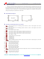
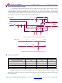
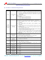
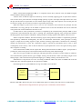
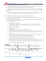
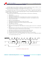
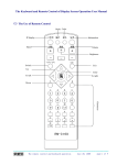
DA32UD User Manual Features ¾ ¾ ¾ ¾ ¾ ¾ ¾ ¾ ¾ ¾ ¾ ¾ ¾ ¾ Apply CS493264 audio DSP, CS8415 96KHz digital receiver, 96 KHz/24bit ADC and DAC. Support Dolby digital, Dolby pro-logic, and DTS and so on, and has various sound field effect playback. Analog audio frequency output, can select low-pass filter circuits by itself so as to realize different effects. Built-in analog input mute, when there is no analog signal, the muting process will automatically go on, there is no need to connect detection circuit outside. Digital and analog ground wires are independent, which lowers the requirement of motherboard PCB LAYOUT and gets better performance. Use different external bass management methods according to different needs and pure hardware filter is able to get wider dynamic range. No DSP effect, user can add different circuits to realize equivalent effects. Use external electronic volume control. Prevent digital audio frequency from deteriorating signal-to-noise ratio when volume is small. Metal case package in the shape of radio head prevents from disturbing sound and other components and provides excellent EMT function. Metal case can be directly installed on the board, being an integrated product with audio board, which improves traditional connection of the decoder board and enhances the reliability and appearance of the product. STL215 singlechip can upgrade directly program online. Users can get new program on Internet when necessary, which provides convenience for debugging and maintenance. Provide mute control signal output and use hardware to mute directly. There are many universal output ports, permitting inner CPU to complete the CTD functions. Provide the SSB communication mode. It is suitable to develop user mainframe by yourself. Application Fields √ Digital audio decoder or analog audio decoder. √ AV reception Power amplifier. √ Multi-channel multimedia active sound box with power supply and decoding. Hard & Soft Technology Co., LTD. http://www.HSAV.com Address: second floor, No.199, Longyin 2nd Road, Xixiang, Shenzhen, China TEL: 86-0755-27951479 27950879 FAX: 86-0755-27950879-213 Business contact:[email protected] Technology support:[email protected] DA32UD User Manual hsavd216.pdf October 26, 2007 Ground Wire Instructions There is no connection between AGND and GND in DA32UD that asked for connecting on the user board. If +5V supply ground wire and analog ground wire are not in the power supply terminal, the connection point should near to the DA32UD pins. GND connects with ground wire of metal outer covering to keep the resistance of ground wire lower for a good effect. Or connecting at the place supplying is also acceptable, while the position nearing the DA32UD pins is preferable for a better effect. DA32UD Dimension Diagram Instructions of The DA32UD Socket Ports Connection 1. 2. 3. 4. 5. 6. 7. 8. 9. 10. 11. 12. 13. 14. 15. 16. 17. 18. 19. 20. 21. SCL Serial clock output port of controlling external volume IC, which is used together with clock of debugging downloading. SDA Serial data output port of controlling external volume IC, which is used together with clock of debugging downloading. PB3 Universal port of input or output. PB2 Universal port of input or output, SCK port of SSB communication port. PB1 Universal port of input or output, SDD port of SSB communication port. PB0 Universal port of input or output, SIN port of SSB communication port. +5V Power supply +5V input. GND Digital ground wire input and output. RX3 Set3 digital input. RX2 Set2 digital input. RX1 Set1 digital input. MUTE MUTE CONTROL SIGNAL OUTPUT. When the mute takes effect it outputs high level, when the sound works normally it outputs low level. SW Extra bass channel signal output. CE Central channel signal output. SR Back right channel signal output. SL Back left channel signal output. FR Front right channel signal output. FL Front left channel signal output. AGND Analog ground wire audio output and power supply input, it does not connected with digital ground and required to be connected from outside. RCH Analog right channel signal input. LCH Analog left channel signal input. © 2002-2009 Hard & Soft Technology Co., LTD. http://www.HSAV.com Page 2 of 8 DA32UD User Manual hsavd216.pdf October 26, 2007 The Instructions of Audio Processing ± Power supply is the best choice for the sake of a good effect ,if power supply of the complete system is ±power supply. Or single power supply can be adopted. When the single power supply is adopted, as the following diagram, operational amplifier plus input connects with 1/2 power supply. If there is no requirement for the sound, operational amplifier is not required and resistor and capacitor filter can be directly applied, while there will not be good effect of signal output range and high frequency. R2 10U R5 4K7 R2 4K7 C1 4 C5 102 6 5 R5 C2 10U LCH 10U RCH 7 IC3-2 NE4570 75R 8 +6V-+24V 221 + C2 - Audio output 15K R2 15K C2 C5 104 10U R5 4K7 R5 4K7 C1 C5 102 R5 2 1K 3 221 1 + C12 - C4 470U IC3-1 NE4570 R5 1K C4 100U C5 104 The Low-pass filter applying single power supply Audio output C12 10U R9 LCH 4K7 C13 102 C2 10U R5 RCH 4K7 C13 102 The Simple type low-pass filter with no power supply Electrical Specification Item Minimum Typical Maximum +5Vpower supply voltage +4.6V +5V +5.5V +5Vworking current (DA32UD) 350mA 360mA 380mA Analog signal input 0.8Vrms 0.9Vrms 1.1Vrms Analog signal output @0dB 0.7Vrms 0.8Vrms 0.9Vrms Digital RX input 0.1V(P-P) 0.5V(P-P) 1.0V(P-P) DA32UD configuration has hardware SSB bus and user’s single-chip communication and applies 8-bit address and 8-bit data. B7 means the seventh of the data, B6 means the sixth of the data, and the rest can be done in the same manner © 2002-2009 Hard & Soft Technology Co., LTD. http://www.HSAV.com Page 3 of 8 DA32UD User Manual hsavd216.pdf October 26, 2007 DA32UD Software Instructions The Table of User Mainframe Writing Instructions Address Function 1) 2) 0x01 Choice of input port 3) 4) 1) 2) 3) 4) 0x02 Normal listening mode Listening mode switching 5) 6) 7) 8) 1) 0x03 Speaker setting and output choice 0x04 Dolby digital dynamic compression 0x05 Speaker delay time adjusting 0x06 0x07 0x08 0x09 0x0a 0x0b © 2002-2009 FL volume modulation FR volume modulation SL volume modulation SR volume modulation CE volume modulation SW volume modulation 2) 3) Data B7 is 1; it is acceptable that signal input automatically mute. When B6 is 1; input port is analog signal input (when AIL and AIK don’t have a signal input, MUTE pin will output high level to mute, usual application should use this function.). When B6 is 0, input port is digital input. B5 to B3 are not used. B1 to B0: 00 means digital is inputted from RX1. 01 means digital is inputted from RX2. 10 means digital is inputted from RX3 When B7 is 0, the mode is plus. When B7 is 1, the mode is PCN effect replaying. B2 to B0=0 is 00H is MATRIX; 01H is LIVE ; 02H is CHURCH ; 03H is STADIUM; 04H is SIMULATED;05H is HALL;06H is CHORUS;07H is THEATRE。 =0 means that has only front left-right speaker replaying, the mode is BYPASS, i.e. 2.0. =1 means that has only front left-central-right speaker replaying, the mode is DOLBY 3 stereo, i.e.3.0. =2 means that has only front and back left-right speaker replaying, the mode is simulation Dolby Pro-Logic, i.e. 2.2. =3 means that has only front left-right and back left-right speaker replaying; the mode is Dolby Pro-Logic, i.e.3.2.If input is Dolby digital AC-3, the mode is Dolby digital; if input is DTS, the mode is DTS digital. B6 is front left-right speaker size choice, 1 is bigB5 is front central speaker size choice, 1 is big speaker. B4 is back left-right speaker size choice, 1 is big speaker. B3 is extra bass speaker configuration choice. 1) Only when the digital code stream inputted is Dolby digital AC-3, this function can take effect. 1) In Dolby digital mode, delay time is 0 to 15 ms; in Dolby Pro-Logic mode, delay time is 15 to 30 ms. Attention: only when the listening mode is Dolby digital or Dolby Pro-Logic, this function can take effect. 0 is 0dB,i.e. the maximum volume; 255 is muting, i.e. the minimum volume. 0 is 0dB,i.e. the maximum volume; 255 is muting, i.e. the minimum volume. 0 is 0dB,i.e. the maximum volume; 255 is muting, i.e. the minimum volume. 0 is 0dB,i.e. the maximum volume; 255 is muting, i.e. the minimum volume. 0 is 0dB,i.e. the maximum volume; 255 is muting, i.e. the minimum volume. 0 is 0dB,i.e. the maximum volume; 255 is muting, i.e. the minimum volume. 2) 1) 1) 1) 1) 1) 1) Hard & Soft Technology Co., LTD. http://www.HSAV.com Page 4 of 8 DA32UD User Manual hsavd216.pdf October 26, 2007 The Table of User Mainframe Reading Instructions Address Function 0x0c The state of signal input Data B1 to B0:(B3 is analog signal indication; if B3 is 1l,there is not analog signal input.) 00 means there is not signal input. 01 means PCM signal input. 10 means Dolby digital code stream signal input. 11 means DTS code stream signal input. The Attention of Listening Mode Choices In BYPASS mode, if digital input has received DOLBY DIGIAL code stream, listening mode is able to enter the DOLBY DIGIAL mode automatically; but if DOLBY DIGITAL contains the Pro-Logic sign internally, listening mode is able to enter the Pro-Logic mode decoding. If choice is not BYPASS, When Analog or Digital PCM signal input is switched to Dolby Digital (not 1+1 voice decoding mode) signal input, Listening mode is able to switch to Dolby Digital automatically. When input is Dolby Digital 1+1 voice decoding mode, Listening mode is able to switch to BYPASS mode. When Dolby Digital signal input is switched to Analog or Digital PCM or Dolby Digital (2/0 voice decoding mode) signal input, Listening mode is able to switch to original the second item or original the third item automatically. In Analog or Digital PCM signal input, only can choose Bypass, 3 Stereo, Pro-Logic modes. In Dolby Digital (1+1 voice decoding mode and 2/0 voice decoding mode) signal input, can choose 3 Stereo, Pro-Logic, Dolby Digital etc. modes. If signal input is Dolby Digital 2/1 signals, no matter the original mode is Bypass or not Bypass, listening mode will switch to Pro-Logic or 3 stereo state automatically. In Dolby Digital (not 1+1 voice decoding mode and 2/0 voice decoding mode) signal input, only can choose Bypass and Dolby Digital modes. Speaker setting state may limit the switching choices of Listening mode: If not having a central speaker, cannot choose 3 stereo mode. If not having a back speaker, cannot choose Pro-Logic mode. © 2002-2009 Hard & Soft Technology Co., LTD. http://www.HSAV.com Page 5 of 8 DA32UD User Manual hsavd216.pdf October 26, 2007 Simple Series Bus Instructions SSB is shorted from Simple Series Bus, it is composed of three lines, SCK bit clock, and SDD bit digital and SIN address latching and interrupt. All three lines of SSB are high level when they are free. Normally applying ports of open-drain structure such as 8051 series ports make the level high through pull-ups. If ports with input and output choices are used, the port will be chosen as input when it’s free and the output is high. Only when output is low level the port will be chosen as output. This is for the convenience of procedure processing. SSB must adapt to ports from 2.5V to 5.0V. In case connection wire between the principal and the subordinate is too long, pull-ups can be added or capacitors from several P to hundreds of P can be connected with ground wire to filter disturbance from the circuit. In SSB, SCK is serial synchronous clock that is outputted by the communication principal. SDD is serial synchronous and bi-directional data. SIN is interrupt port subordinate applying from principal and address latching signal from principal to subordinate. When principal is sending signals to the address, the level is low. SSB is composed of address, data and answering signal, among which the address is outputted by principal and inputted by subordinate unchangeably; the data is bi-directional transmission, when principal is writing register is output and is reading register is input; And the answering signal offers a mechanism for confirming whether the transmission is right; The confirmation signal is initiated by subordinate and its value is fixed unchangeably as the contrary value of the last data bite. If principal doesn’t receive the right answering signal, then it requires re-sending. In the transmission of SSB, low bit outputs first. During the transmission of address signal,principal has to put SIN low, while in the process of transmission data and answering must make SIN high. There are two types of SSB: low speed type and high-speed type, two kinds of control modes are identical. The communication speed of the low type is 33Kbps, namely, each SCK time is 30US (one falling margin to next falling margin). The communication speed of the high type is 1Mbps, namely, each SCK time is 1us. SSB address is composed of 4 to 8 bits. According to different address bits, there are SSB4 with 4 bits and SSB8 with 8 bits. DA32UD applies the low speed bus of SSB4. DA32UD applies low speed SSB4 bus having 4-bit address and 8-bit data. Principal (user’s mainframe) SCK PB2 SDD PB1 SIN PB0 Subordinate Attention: PB0, PB1, PB2 are the pins on the motherboard (please according to the silk-screen of motherboard) SSB Connection diagram between principal (user’s mainframe) and subordinate © 2002-2009 Hard & Soft Technology Co., LTD. http://www.HSAV.com Page 6 of 8 DA32UD User Manual hsavd216.pdf October 26, 2007 The Instructions of SSB4 Low-speed Bus Used by DA32UD In DA32UD communication process, the principal is single-chip machine used by the user shorted to be user mainframe. The subordinate is DSP used by DA32UD, shorted to be DA32UD. Suggesting apply the port without input and output control port to communicate. If user mainframe has input and output two choices, only when low level is outputted the choice is output. Such can automatically adapt to SSB level. DA32UD uses 16 registers, the length of address is 4 bits, register 0x00 is writing register, and the length of data is 8 bits, i.e. 1 byte. Register 0x0e to 0x0f are usual registers; the length is 16 bits, i.e. 2 bytes. The Time Order Instructions of Writing Register of SSB4 Bus Used by DA32UD DA32UD applies the low speed bus of SSB4; has 16 registers aggregately, the length of address is 4 bits, and the length of data is 8 bits, i.e. 1 byte. When the user mainframe writes register, 4-bit address should be written first and low bit should output first. Time order of writing register is as following: 1. Make SIN low. 2. Output A0 bit of the address first. 3. Make SCK low and delay time to a corresponding time (low speed is 15us, high speed is 0.5us). 4. Make SCK high and delay time to a corresponding time (low speed is 15us, high speed is 0.5us). 5. Output A1 bit of the address. 6. Repeat 3 to 5 until finishing A7 bit. 7. Make SIN high. 8. Output D0 bit and repeat action of the SCK until finishing D7 bit. 9. Make SDD high and turn SDD into input, which is in order to prepare for receiving answering bit. 10. Make SCK low and delay time, when subordinate will output opposite code of D7 as confirmation signal. 11. Make SCK high and when delaying time have finished contrast with the value of reading SDD. If the comparison result is opposite, it means the data is read successfully. 12. Make SCK low and delay time, this moment subordinate output SDD as high. 13. After making SCK high and delaying time, the register writing is finished. 14. If writing is not successful, it will begin rewriting until instructions are written correctly. 15. Attention: No matter SIN is high or low, when SCK turns low at the first time, DA32UD will output SIN as high. If some error with writing and reading, when the bus is free the subordinate will turn low again to send interrupt signals to the principal. SCK SDD A0 A3 A1 D0 D1 D7 ACK SIN User mainframe writing register orders © 2002-2009 Hard & Soft Technology Co., LTD. http://www.HSAV.com Page 7 of 8 DA32UD User Manual hsavd216.pdf October 26, 2007 The Time Order Instructions of Reading Register of SSB Bus DA32UD applies the low speed bus of SSB4; has 16 registers aggregately, the length of address is 4 bits, register 0x0e to 0x0f are reading registers, and the length of data is 8 bits, i.e. 1 byte. When SIN becomes low, Principal can read register, or can read register at the any time, but when SIN is low, if principal reads register, it has to first read interrupt register in order to judge that which register has initiated interrupt, moreover, has to read corresponding register or writing corresponding shield number to clear interrupt, or SIN may often change low. Principal first writes register waiting for being read. The orders of transmission is the following: 1. Make SIN low. 2. Output A0 bit of the address first. 3. Make SCK low and delay time to a corresponding time (low speed is 15us, high speed is 0.5us). 4. Make SCK high and delay time to a corresponding time (low speed is 15us, high speed is 0.5us). 5. Output A1 bit of the address. 6. Repeat 2 to 5 until finishing A3 bit. 7. Output SDD, make SDD become input, be ready to receive data. 8. Make SCK low and delay time, this moment subordinate sends DO to SDD. 9. Make SDD high, read DO bit. 10. Repeat 8 to 9 until receiving D7 completely. 11. Make SCK low and delay time, when subordinate will output opposite code of D7 as confirmation signal 12. Make SCK high and when delaying time have finished contrast with the value of reading SDD. If the comparison result is opposite, it means the data is read successfully. 13. Make SCK low and delay time, this moment subordinate output SDD as high. 14. After making SCK high and delaying time, the register reading is finished. 15. If reading is not successful, it will begin rereading until instructions are read correctly. 16. In register address 0x0e to 0x0f, the length of data is fix as 1 byte 8 bits in all. Adding 4 bits address and 1 bit answering total up to 13 bits. SCK SDD A0 A1 A3 D0 D1 D7 ACK SIN User mainframe reading register orders © 2002-2009 Hard & Soft Technology Co., LTD. http://www.HSAV.com Page 8 of 8