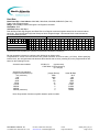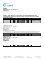
1
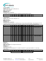
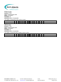
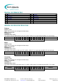
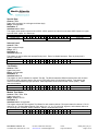
Model 64RS2
Twelve (12) Synchronous/Asynchronous
RS-232C, RS-422, RS-485 Channels
VMEbus CONTROL
SERIAL COMMUNICATION CARD
TWELVE, EIGHT, or FOUR INDEPENDENT & PROGRAMMABLE
RS-232C, RS-422, RS-485
SYNCHRONOUS or ASYNCHRONOUS
For Commercial or Military Applications
FEATURES
Typical Configuration
• Independent full-duplex synchronous or
asynchronous channels
• High Data Rate (8 Mbps synchronous, 800 Kbps
asynchronous)
• Programmable for RS-232C, RS-422, RS-485
• Hardware data transfers minimize data latency
• Power-on loop-back self-test
• Watchdog timer and soft reset
• I/O via front panel, P2 or both
• Part Number, S/N, Date Code, & Revision in nonvolatile memory
• Conforms to ANSI/VITA 1.1-1997 VME64 extension
• Conforms to VITA 1-1994
• VxWorks Library and Driver Available
Typical Configuration
DESCRIPTION
This sophisticated, high-speed, DSP-based card incorporates up to twelve (12) intelligent, full duplex communications
channels that can be individually software configured for RS-232C, RS-422 or RS-485 Synchronous or Asynchronous
Communication. The architecture avoids latency problems because all data transfer is done in hardware and not in
software. DSP runs at 160 MHz and only handles background tasks such as interrupt generation. Any incoming data,
no matter how many channels are active, in whatever mode, can be immediately extracted. A BREAK sequence
capability is also incorporated. Bus Data is transferred within 300 ns. A layer of software isolates the user from
UART idiosyncrasies thus simplifying programming and usage.
An Internal Loop Back Self Test is performed when power is applied and results are stored in registers. During Loop
Back test, the outputs are disconnected. Each channel can be programmed into a Loop Back mode that internally
wraps the transmitter to the receiver without the need of external wiring. Output short circuit capability is continuous and
bullet proof. If the card is not powered, neither the inputs nor outputs will load down the lines. Inputs and outputs can
withstand ±15 volts under any condition. All serial lines are transient protected to IEC1000 4-2, 4-4, & 4-5.
Serial Data Transmit Enhancement: An additional asynchronous mode to support “Immediate Transmit” operation
has been incorporated. This mode immediately transmits serial data anytime the transmit buffer is not empty. There is
no requirement to set the “TX Initiate” bit after each byte where VME traffic and overhead can be simplified since only
the actual data byte being transmitted needs be sent to the transmit buffer. Each channel has its own 64kbyte
Transmit and Receive buffer.
While in Asynchronous mode, the upper byte of each received word provides status information for that word.
Receiver Enable/Disable: A Receiver Enable/Disable function allows the user to turn selected receivers ON/OFF.
When a receiver is disabled, no data will be placed in the buffer. (Card is shipped with all receivers enabled).
DSR capability is available for channels 1-6 via P2 & P0, and for channels 1-12 from front panel connectors.
CRC code generation and detection is also available for message integrity when used in Synchronous, HDLC and
Asynchronous PPP modes.
North Atlantic Industries, Inc.
110 Wilbur Place, Bohemia, NY 11716
631.567.1100/631.567.1823 (fax)
www.naii.com / e-mail:[email protected]
1/3/08
Cage Code:OVGU1
64RS2_A001_Rev_2.1
Page 1 of 29
This serial card can operate in an Interrupt Driven Environment to provide notification of all events to the system. It
supports hardware flow control (CTS/RTS and/or DCD/DTR) as well as software flow control (XON, XOFF). When a
flow control mode is selected, the serial card does the operation automatically with minimal system intervention.
A Parity Error Interrupt is provided for each single byte throughout the communications data stream.
Multi-Drop Link Mode: The transmitter and receivers of up to 32 cards can be tied together in either Half or Full
Duplex mode. While in Multi-Drop Link Mode, the transmit line for each channel will automatically change from tristate to enable to transmit any data as soon as it is placed in the transmit buffer. Once transmission is completed, the
transmit line is automatically changes back to tri-state mode.
For redundant applications, this card can be paralleled with another card to offer redundancy. User provided
software control is required to drive one output ON at time during data transmission. No two or more cards in parallel
should transmit simultaneously. Output levels are in “tri-state” while transmission is inactive.
Geographical addressing can be implemented
A watchdog timer is provided to monitor processor activity.
To simplify logistics, Part number, Serial number, Date code and Rev Level are stored in non-volatile memory
locations.
A VxWorks Software Communications Driver & Library is available from our WEB site http://www.naii.com.
A current, updated soft copy of this manual is also available at our web site.
North Atlantic Industries, Inc.
110 Wilbur Place, Bohemia, NY 11716
631.567.1100/631.567.1823 (fax)
www.naii.com / e-mail:[email protected]
1/3/08
Cage Code:OVGU1
64RS2_A001_Rev_2.1
Page 2 of 29
SPECIFICATIONS
Number of channels:
Data rate:
Twelve (12) fully programmable
8 Mbits/s per channel in Synchronous/HDLC mode
800kbits/s per channel in Asynchronous mode (RS-422 & RS-485)
Data can be read 4µs after receipt in UART.
These data rates are verified with all channels running simultaneously.
Asynchronous and synchronous (internal clock) Bit Rate Generation limitation(s):
Bit rate generation is based on a primary clock divided by an integer value.
Programmed bit versus actual bit rate will have greater resolution at lower bit rates
(<115 KHz). When specifying internal clock, the card generates and transmits the
actual bit rate as close (rounding off) to the programmed bit rate based on the following
formula:
Actual bit rates available:
Asynchronous examples:
Programmed Bit Rate (b/s)
381 (minimum)
600
2400
9600
57600
115200
300000
600000
800000 (maximum)
25 MHz / N
(synchronous)
1.5625 MHz / N (asynchronous)
(N = integer)
(Integer Divisor)
4096
2604
651
163
27
14
5
3
2
Actual Bit Rate
381.5
600
2400
9586
57870
111607
312500
520883
781250
Note: Bit generation formulas may differ between product models.
VME Data transfer:
Receive/Transmit buffers:
Interrupts:
Power:
Temperature, operating:
Storage temperature:
Base address:
Size:
Weight:
North Atlantic Industries, Inc.
110 Wilbur Place, Bohemia, NY 11716
Data transfers within 300 ns.
64 Kbytes for each Receive and Transmit buffer. Accessed in 16 bit mode only.
1 vector per channel
+5 VDC, 1A per module (Mode dependant: RS232 has lower power req’ts, RS422 more)
C" 0°C to +70°C, "E" -40°C to +85°C (See part number)
-40°C to +105°C.
Geographical addressing can be implemented. Otherwise, board dip switches are
activated for setting base address.
(9.2") H, 4HP (0.8") W. 233.4 x 20.3 x 160 mm deep
22 oz.
631.567.1100/631.567.1823 (fax)
www.naii.com / e-mail:[email protected]
1/3/08
Cage Code:OVGU1
64RS2_A001_Rev_2.1
Page 3 of 29
I/O CONFIGURATION:
The VME bus interface will respond to A32:D16, A24:D16 and A16:D16 DTB cycles.
A32 mode: Unit responds to address modifiers 0A, 0D, 0E and 09. Base address can be set anywhere in the 4
Gigabyte address space on 512 byte boundaries.
A24 mode: Responds to address modifiers 3A, 3D, 3E and 39. Base address can be set anywhere in the 16 Megabyte
address space on 512 byte boundaries.
A16 mode: Responds to address modifiers 2A, 2D, 2E and 29. Base address can be set anywhere in the 64 K byte
address space on 512 byte boundaries.
Note: Address switch A8, A9 & A10 must be set to "ON" for 2048 byte boundaries (SW1.1, SW1.2, & SW1.3)
Enable Geographical Addressing by removing jumper from JP2. Disable by adding jumper to JP2.
GEOGRAPHICAL ADDRESSING
Geographical Addressing may be implemented implemented. This card will respond to address modifier 2Fh for A24
Address mode, where the 5 Msb’s of the A24 address are the 5 bits defined by the slot in VME back plane. The Card
can optionally be interrogated at 2Fh to determine resource requirements and available functionally. Using the address
modifier 2Fh, the following need to be written to the card:
1) The base address the card should respond to
2) The address modifier (A16, A24, A32)
3) Then enable the card.
For example: If the card is in slot # 10 the 5 Msb’s are 01010 so the address of the CSR registers are:
0101 0 111 1111 1111 xxxx xxxx or 57FFxx h ( xx is CSR register offset)
Write to address 57FF63 h, the A31 – A24 base address bits, for example 01h
Write to address 57FF67 h, the A23 – A16 base address bits, for example 02h
Write to address 57FF6B h, the A15 – A8 base address bits, for example 04h
Write to address 57FF6F h, the address modifier you wish to respond to shifted up 2 bits, ex. 28h(0A<< 2)
then write to address 57FFFBh, 10h to enable the card.
The card will now respond to the base address (010204 in the example) and address modifier (0A in example)
programmed. The base address and address modifier can be changed at any time.
PRODUCT CONFIGURATION AND MEMORY MAP
This card is populated with up to 3 modules of 4 Serial Communication Channels. As such, the card can be configured
as a 4, 8 or 12 channel card. The memory map of each module counts from, or is superimposed over, its respective
module offset (1 through 3).
Address = Base + Module Offset + Register Offset.
For example: Address = Base + Module 2 offset 200 + MRS2 register 00C = Base + 20C hex.
MEMORY MAP
000 Module 1 Register…
002
004
006
008
.
.
.
1FC
Channels 1-4
1FE
Module 1
Offset 000
200 Module 2 Register…
202
204
206
208
.
.
.
3FC
Channels 5-8
3FE
Module 2
Offset 200
400 Module 3 Register…
402
404
406
408
.
.
.
5FC
Channels 9-12
5FF
Module 3
Offset 400
The memory map of the 4 channel Serial Communications module is described hereafter:
North Atlantic Industries, Inc.
110 Wilbur Place, Bohemia, NY 11716
631.567.1100/631.567.1823 (fax)
www.naii.com / e-mail:[email protected]
1/3/08
Cage Code:OVGU1
64RS2_A001_Rev_2.1
Page 4 of 29
MODULE MEMORY MAP – 4 CHANNEL SERIAL COMMUNICATIONS (P1)
000
002
004
006
00C
00E
010
012
018
01A
01C
01E
024
026
028
02A
030
032
034
036
03C
03E
040
042
048
04A
04C
04E
054
056
058
05A
05C
05E
060
062
06C
06E
070
072
Tx Buffer Chan 1
W
Tx Buffer Chan 2
W
Tx Buffer Chan 3
W
Tx Buffer Chan 4
W
Rx Buffer Chan 1
R
Rx Buffer Chan 2
R
Rx Buffer Chan 3
R
Rx Buffer Chan 4
R
Number Of Words Tx Buffer Chan 1 R
Number Of Words Tx Buffer Chan 2 R
Number Of Words Tx Buffer Chan 3 R
Number Of Words Tx Buffer Chan 4 R
Number Of Words Rx Buffer Chan 1 R
Number Of Words Rx Buffer Chan 2 R
Number Of Words Rx Buffer Chan 3 R
Number Of Words Rx Buffer Chan 4 R
Protocol Chan 1
W
Protocol Chan 2
W
Protocol Chan 3
W
Protocol Chan 4
W
Clock Mode Chan 1
W
Clock Mode Chan 2
W
Clock Mode Chan 3
W
Clock Mode Chan 4
W
Interface Levels Chan 1
W
Interface Levels Chan 2
W
Interface Levels Chan 3
W
Interface Levels Chan 4
W
Tx-Rx Configuration Low Chan 1 R/W
Tx-Rx Configuration High Chan 1 R/W
Tx-Rx Configuration Low Chan 2 R/W
Tx-Rx Configuration High Chan 2 R/W
Tx-Rx Configuration Low Chan 3 R/W
Tx-Rx Configuration High Chan 3 R/W
Tx-Rx Configuration Low Chan 4 R/W
Tx-Rx Configuration High Chan 4 R/W
Channel Control Low Chan 1
R/W
Channel Control High Chan 1
R/W
Channel Control Low Chan 2
R/W
Channel Control High Chan 2
R/W
074
076
078
07A
084
086
088
08A
090
092
094
096
098
09A
09C
09E
0A8
0AA
0AC
0AE
0B4
0B6
0B8
0BA
0C0
0C2
0C4
0C6
0CC
0CE
0D0
0D2
0D8
0DA
0DC
0DE
0E4
0E6
0E8
0EA
Channel Control Low Chan 3
R/W
Channel Control High Chan 3
R/W
Channel Control Low Chan 4
R/W
Channel Control High Chan 4
R/W
Data Configuration Chan 1
R/W
Data Configuration Chan 2
R/W
Data Configuration Chan 3
R/W
Data Configuration Chan 4
R/W
Baud Rate Low Chan 1
R/W
Baud Rate High Chan 1
R/W
Baud Rate Low Chan 2
R/W
Baud Rate High Chan 2
R/W
Baud Rate Low Chan 3
R/W
Baud Rate High Chan 3
R/W
Baud Rate Low Chan 4
R/W
Baud Rate High Chan 4
R/W
Preamble Chan 1
R/W
Preamble Chan 2
R/W
Preamble Chan 3
R/W
Preamble Chan 4
R/W
Tx Buffer Almost Empty Chan 1 R/W
Tx Buffer Almost Empty Chan 2 R/W
Tx Buffer Almost Empty Chan 3 R/W
Tx Buffer Almost Empty Chan 4 R/W
Rx Buffer Almost Full Chan 1
R/W
Rx Buffer Almost Full Chan 2
R/W
Rx Buffer Almost Full Chan 3
R/W
Rx Buffer Almost Full Chan 4
R/W
Rx Buffer High Watermark Chan 1 R/W
Rx Buffer High Watermark Chan 2 R/W
Rx Buffer High Watermark Chan 3 R/W
Rx Buffer High Watermark Chan 4 R/W
Rx Buffer Low Watermark Chan 1 R/W
Rx Buffer Low Watermark Chan 2 R/W
Rx Buffer Low Watermark Chan 3 R/W
Rx Buffer Low Watermark Chan 4 R/W
HDLC Address/Sync Char Chan 1 R/W
HDLC Address/Sync Char Chan 2 R/W
HDLC Address/Sync Char Chan 3 R/W
HDLC Address/Sync Char Chan 4 R/W
0F0
0F2
0F4
0F6
0FC
0FE
100
102
108
10A
10C
10E
114
116
118
11A
120
122
124
126
180
182
184
186
18C
18E
190
192
198
19A
19C
19E
1A4
1A6
1A8
1AA
1F8
1FC
1FE
Termination Character Chan 1
Termination Character Chan 2
Termination Character Chan 3
Termination Character Chan 4
XON Character Chan 1
XON Character Chan 2
XON Character Chan 3
XON Character Chan 4
XOFF Character Chan 1
XOFF Character Chan 2
XOFF Character Chan 3
XOFF Character Chan 4
FIFO Status Chan 1
FIFO Status Chan 2
FIFO Status Chan 3
FIFO Status Chan 4
Time Out Value Chan 1
Time Out Value Chan 2
Time Out Value Chan 3
Time Out Value Chan 4
Interrupt Enable Chan 1
Interrupt Enable Chan 2
Interrupt Enable Chan 3
Interrupt Enable Chan 4
Interrupt Status Chan 1
Interrupt Status Chan 2
Interrupt Status Chan 3
Interrupt Status Chan 4
Interrupt Vector Chan 1
Interrupt Vector Chan 2
Interrupt Vector Chan 3
Interrupt Vector Chan 4
Channel Status 1
Channel Status 2
Channel Status 3
Channel Status 4
Module ID
FPGA Version
DSP Version
R/W
R/W
R/W
R/W
R/W
R/W
R/W
R/W
R/W
R/W
R/W
R/W
R
R
R
R
R/W
R/W
R/W
R/W
R/W
R/W
R/W
R/W
R/W
R/W
R/W
R/W
R/W
R/W
R/W
R/W
R
R
R
R
R
R
R
Serial Communications Module register programming and its associated Bit Map is as follows:
North Atlantic Industries, Inc.
110 Wilbur Place, Bohemia, NY 11716
631.567.1100/631.567.1823 (fax)
www.naii.com / e-mail:[email protected]
1/3/08
Cage Code:OVGU1
64RS2_A001_Rev_2.1
Page 5 of 29
MODULE REGISTER DEFINITIONS
Transmit Buffer
Address: 000h, 002h, 004h, 006h (Chan.1-4)
Type: unsigned character word
Range: 00h or FFh (low byte)
Read/Write: W
Initialized Value: Not Applicable
This register is the transmit data buffer. Data intended to be transmitted must be placed here prior to transmission.
Data words are 8-bit and occupy the register’s lowest significant bits (lsbs), or low byte. See bit map below:
REGISTER
TRANSMIT BUFFER
D15 D14 D13 D12 D11 D10 D9 D8 D7 D6 D5 D4 D3 D2 D1 D0
X
X
X
X
X
X
X
X
D
D
D
D
D
D
D
D
FUNCTION
X=DON'T CARE, D=DATA BIT
Receive Buffer
Address: 00Ch, 00Eh, 010h, 012h (Chan.1-4)
Type: unsigned integer word.
Range: 00h or FFh (for low byte and for high byte)
Read/Write: R
Initialized Value: Not Applicable
This register is the receive data buffer. Data is received in the low byte as unsigned integer. The high byte is used
for status.
REGISTER
RECEIVE BUFFER
Asynchronous
D15 D14 D13 D12 D11 D10 D9 D8 D7
S
S
S
S
S
S
S
D
D6
D5
D4 D3 D2 D1 D0
D
D
D
D
D
D
S=STATUS BIT, D=DATA BIT
EOF only if Termination Char is used
X
X
X
X EOF P
D
D
D
D
D
D
D
D
X
X
X
X
X
X EOF X
D
D
D
D
D
D
D
D
HDLC Mode
X
X
X
X
X
X EOF X VFR RDO CRC RAB X
X
C/R
X
= Parity Error
= Framing Error
= End Of Frame
= Parity Bit
= Valid Frame
= Receive Data Overflow
= CRC Compare/Check
= Receive msg Aborted
= Command/Response
FUNCTION
D
Bi/Mono Synchronous
PE
FE
EOF
P
VFR
RDO
CRC
RAB
C/R
PE FE
S
Last Word is Status Word
‘1’ Calculated parity does not match the received parity bit
‘1’ A character framing error was detected.
‘1’ Indicates End of Frame. Useful to identify multiple frames in large buffer
This bit carries the parity bit of the last received character
‘0’ Received fame is invalid
‘0’ No data overflow has occurred
‘1’ Overflow
‘0’ Fail; Received frame contains errors
‘1’ Pass; No CRC errors in received frame.
‘0’ No abort condition detected
‘1’ Receive frame was aborted.
Only significant for 2 byte address mode.
Number of Words Tx Buffer
Address: 018h, 01Ah, 01Ch, 01Eh (Chan.1-4)
Type: unsigned integer word
Range: 0 to 65535
Read/Write: R
Initialized Value: 0
This register contains the number of words to be transmitted.
REGISTER
D15 D14 D13 D12 D11 D10 D9 D8 D7 D6 D5 D4 D3 D2 D1 D0
NUM WORDS TX BUFFER D
D
North Atlantic Industries, Inc.
110 Wilbur Place, Bohemia, NY 11716
D
D
D
D
D
D
D
D
D
631.567.1100/631.567.1823 (fax)
www.naii.com / e-mail:[email protected]
D
D
D
D
D
1/3/08
Cage Code:OVGU1
FUNCTION
D=DATA BIT
64RS2_A001_Rev_2.1
Page 6 of 29
Number of Words Rx Buffer
Address: 024h, 026h, 028h, 02Ah (Chan.1-4)
Type: unsigned integer word
Range: 0 to 65535
Read/Write: R
Initialized Value: 0
This register contains the number of words to be received.
REGISTER
D15 D14 D13 D12 D11 D10 D9 D8 D7 D6 D5 D4 D3 D2 D1 D0
NUM WORDS RX BUFFER D
D
D
D
D
D
D
D
D
D
D
D
D
D
D
FUNCTION
D
D=DATA BIT
Protocol
Address: 030h, 032h, 034h, 036h (Chan.1-4)
Type: unsigned integer word
Range: 0 to 5
Read/Write: W
Initialized Value: 0, Asynchronous
This register is used to configure the associated channel for either asynchronous, mono-synchronous, bisynchronous, or HDLC, PPP-asynchronous, Extended Transparent communications mode.
REGISTER
PROTOCOL
D15 D14 D13 D12 D11 D10 D9 D8 D7 D6 D5 D4 D3 D2 D1 D0
FUNCTION
0
0
0
0
0
0
0
0
0
0
0
0
0
0
0
0
ASYNC
0
0
0
0
0
0
0
0
0
0
0
0
0
0
0
1
MONO-SYNC
BI-SYNC
0
0
0
0
0
0
0
0
0
0
0
0
0
0
1
0
0
0
0
0
0
0
0
0
0
0
0
0
0
0
0
0
0
0
0
0
0
0
0
0
0
0
0
1
1
HDLC
1
0
0
PPP-ASYNC
0
0
0
0
0
0
0
0
0
0
0
0
0
1
0
1
EXTENDED TRANSPARENT
Clock Mode
Address: 03Ch, 03Eh, 040h, 042h (Chan.1-4)
Type: unsigned integer word
Range: 0 to 5
Read/Write: W
Initialized Value: 0
This register configures for internal or external transmit/receive clocks. To transmit or output clock signal on
channel clock pin, program TXCLK VISIBLE (0x8000).
REGISTER
CLOCK MODE
D15 D14 D13 D12 D11 D10 D9 D8 D7 D6 D5 D4 D3 D2 D1 D0
FUNCTION
0
0
0
0
0
0
0
0
0
0
0
0
0
0
0
0
TX-INTERNAL , RX-INTERNAL
0
0
0
0
0
0
0
0
0
0
0
0
0
0
0
1
TX-CLKA , RX-INTERNAL
0
0
0
0
0
0
0
0
0
0
0
0
0
0
1
0
TX-INTERNAL , RX-CLKB
1
1
TX-CLKA , RX-CLKA
0
0
0
0
0
0
0
0
0
0
0
0
0
0
0
0
0
0
0
0
0
0
0
0
0
0
0
1
0
0
TX-CLKB , RX-CLKB
0
0
0
0
0
0
0
0
0
0
0
0
0
1
0
1
TX-CLKA , RX-CLKB
1
0
0
0
0
0
0
0
0
0
0
0
0
0
0
0
TX-CLK VISIBLE
North Atlantic Industries, Inc.
110 Wilbur Place, Bohemia, NY 11716
631.567.1100/631.567.1823 (fax)
www.naii.com / e-mail:[email protected]
1/3/08
Cage Code:OVGU1
64RS2_A001_Rev_2.1
Page 7 of 29
Interface Levels
Address: 048h, 04Ah, 04Ch, 04Eh (Chan.1-4)
Type: unsigned integer word
Range: 0 to 4
Read/Write: W
Initialized Value: 5
This register is used to configure the interface level (RS232, RS422, RS485, Loop Back, or Tri-State) for the
associated channel. Loop Back selection connects the channel’s transmit and receive line internally. To implement,
user must send data and look at Receive FIFO to verify that the sent data. Loop Back is usually used for test.
REGISTER
INTERFACE LEVELS
D15 D14 D13 D12 D11 D10 D9 D8 D7 D6 D5 D4 D3 D2 D1 D0
FUNCTION
0
0
0
0
0
0
0
0
0
0
0
0
0
0
0
0
RS232
0
0
0
0
0
0
0
0
0
0
0
0
0
0
0
1
RESERVED
0
0
0
0
0
0
0
0
0
0
0
0
0
0
1
0
RS422
0
0
0
0
0
0
0
0
0
0
0
0
0
0
1
1
RS485
0
0
0
0
0
0
0
0
0
0
0
0
0
0
0
0
0
0
0
0
0
0
0
0
0
0
1
1
0
0
0
1
MANUAL LOOP BACK
TRI-STATE
North Atlantic Industries, Inc.
110 Wilbur Place, Bohemia, NY 11716
631.567.1100/631.567.1823 (fax)
www.naii.com / e-mail:[email protected]
1/3/08
Cage Code:OVGU1
64RS2_A001_Rev_2.1
Page 8 of 29
Tx-Rx Configuration Low
Address: 054h, 058h, 05Ch, 060h (Chan.1-4)
Type: binary word
Range: not applicable
Read/Write: R/W
Initialized Value: 0
This register is used to set the transmit/receive configuration for the associated channel. Functions depend upon
programmed protocol (see Protocol Register).
REGISTER
Tx-Rx CONFIG LO
D15 D14 D13 D12 D11 D10 D9 D8 D7 D6 D5 D4 D3 D2 D1 D0
FUNCTION
0
0
0
0
0
0
0
0
0
0
0
0
0
0
0
1
“1” = RTS/CTS FLOW CONTROL
0
0
0
0
0
0
0
0
0
0
0
0
0
0
1
0
0
0
0
0
0
0
0
0
0
0
0
0
0
1
0
0
0
0
0
0
0
0
0
0
0
0
0
0
1
0
0
0
0
0
0
0
0
0
0
0
0
0
0
1
0
0
0
0
0
0
0
0
0
0
0
0
0
0
1
0
0
0
0
0
0
0
0
0
0
0
0
0
0
1
0
0
0
0
0
0
0
0
0
0
0
0
0
0
1
0
0
0
0
0
0
0
0
0
0
0
0
0
0
1
0
0
0
0
0
0
0
0
0
0
0
0
0
0
1
0
0
0
0
0
0
0
0
0
0
0
0
0
0
1
0
0
0
0
0
0
0
0
0
0
0
0
0
0
1
0
0
0
0
0
0
0
0
0
0
0
0
0
0
1
0
0
0
0
0
0
0
0
0
0
0
0
0
0
1
0
0
0
0
0
0
0
0
0
0
0
0
0
0
1
0
0
0
0
0
0
0
0
0
0
0
0
0
0
1
0
0
0
0
0
0
0
0
0
0
0
0
0
0
0
“1” = DTR/DSR FLOW CONTROL
“1” = AUTO TRANSMIT MODE
ENABLED
RTS FUNCTION
“0” = WATERMARK
“1” = TxDATA AVAIL
“1” = CARRIER DETECT FLOW
CONTROL
CARRIER DETECT PIN POLARITY
“1” = ACTIVE LOW
“0” = ACTIVE HIGH
“1” = ADDRESS RECOGNITION
(HDLC ONLY)
ADDRESS LENGTH (HDLC ONLY)
“1” = 16
“0” = 8 BITS
“1” = HIGH BYTE RECOGNITION
(HDLC ONLY)
ADDRESS AS DATA (HDLC ONLY)
“0” = STRIPPED
“1” = KEPT
SYNC CHAR LENGTH
“0” = (6) MONO,(12) Bi-Sync
“1” = (8 )MONO,(16) Bi-Sync
SYNC CHAR AS DATA
“0” = STRIPPED
“1” = KEPT
“1” = TERMINATION CHAR
DETECTION
“1” = XON/XOFF FLOW CONTROL
XON/XOFF CHAR AS DATA
“0” = STRIPPED
“1” = KEPT
“1” = TIME OUT DETECTION
North Atlantic Industries, Inc.
110 Wilbur Place, Bohemia, NY 11716
631.567.1100/631.567.1823 (fax)
www.naii.com / e-mail:[email protected]
1/3/08
Cage Code:OVGU1
64RS2_A001_Rev_2.1
Page 9 of 29
Tx-Rx Configuration High
Address: 056h, 05Ah, 05Eh, 062h (Chan.1-4)
Type: binary word
Range: not applicable
Read/Write: R/W
Initialized Value: 0
This register is used to configure CRC function and OPEN and IDLE flags. In HDLC mode, error protection is done
by CRC generation and checking. The frame sequence at the end of each frame consisted of two or four bytes of
CRC checksum. 32-bit or CCITT algorithms can be selected.
REGISTER
Tx-Rx CONFIG HI
D15 D14 D13 D12 D11 D10 D9 D8 D7 D6 D5 D4 D3 D2 D1 D0
0
0
0
0
0
0
0
0
0
0
0
0
0
0
0
1
0
0
0
0
0
0
0
0
0
0
0
0
0
0
1
0
0
0
0
0
0
0
0
0
0
0
0
0
0
1
0
0
0
0
0
0
0
0
0
0
0
0
0
0
1
0
0
0
0
0
0
0
0
0
0
0
0
0
0
1
0
0
0
0
0
0
0
0
0
0
0
0
0
0
1
0
0
0
0
0
0
0
0
0
0
0
0
0
0
1
0
0
0
0
0
0
FUNCTION
CRC RESET VALUE (HDLC ONLY)
“1” = 0000 or 00000000
“0” = FFFF or FFFFFFFF
CRC SELECT
HDLC : “1” = 32BIT CRC
“0” = 16BIT CRC-CCITT
SYNC : 1” = 16BIT CRC-CCITT
“0” = 16BIT CRC
“1” = APPEND CRC TO TxDATA
RxCRC AS DATA (HDLC ONLY)
“0” = STRIPPED
“1” = KEPT
“1” = SHARED FLAGS TRANSMISSION
(HDLC ONLY)
“1” = IDLE FLAGS TRANSMISSION
DATA INVERSION
“0” = NORMAL
“1” = INVERTED
Channel Control Low
Address: 06Ch, 070h, 074h, 078h (Chan.1-4)
Type: binary word
Range: not applicable
Read/Write: R/W
Initialized Value: 0
This register is used to for channel control configuration.
REGISTER
CONTROL LO
D15 D14 D13 D12 D11 D10 D9 D8 D7 D6 D5 D4 D3 D2 D1 D0
0
0
0
0
0
0
0
0
0
0
0
0
0
0
0
1
FUNCTION
RTS/GPIO 11
CTS/GPIO 21
0
0
0
0
0
0
0
0
0
0
0
0
0
0
1
0
0
0
0
0
0
0
0
0
0
0
0
0
0
1
0
0
0
0
0
0
0
0
0
0
0
0
0
0
1
0
0
0
0
0
0
0
0
0
0
0
0
0
0
1
0
0
0
0
0
0
0
0
0
0
0
0
0
0
1
0
0
0
0
0
Tx INITIATE2
0
0
0
0
0
0
0
0
0
1
0
0
0
0
0
0
Tx ALWAYS (ASYNC ONLY)
0
0
0
0
0
0
0
0
1
0
0
0
0
0
0
0
RESERVED
0
0
0
0
0
0
0
1
0
0
0
0
0
0
0
0
TRISTATE TRANSMIT LINE
0
0
0
0
0
0
1
0
0
0
0
0
0
0
0
0
ENABLE RECEIVER
0
0
0
0
0
1
0
0
0
0
0
0
0
0
0
0
SET/RELEASE BREAK
0
0
0
0
1
0
0
0
0
0
0
0
0
0
0
0
ENTER HUNT MODE
0
0
0
1
0
0
0
0
0
0
0
0
0
0
0
0
TIMEOUT ENABLE
0
0
1
0
0
0
0
0
0
0
0
0
0
0
0
0
0
1
0
0
0
0
0
0
0
0
0
0
0
0
0
0
1
0
0
0
0
0
0
0
0
Notes: 1. Disable D0 through D4 to enter GPIO control.
RTS/CTS as GPIO when RTS/CTS Flow Control disabled.
DTR/DSR as GPIO when DTR/DSR Flow Control disabled.
2. Firmware will clear bit when done.
0
0
0
0
0
0
0
North Atlantic Industries, Inc.
110 Wilbur Place, Bohemia, NY 11716
631.567.1100/631.567.1823 (fax)
www.naii.com / e-mail:[email protected]
DTR/GPIO 31
DSR/GPIO 41
DCD/GPIO 51
RESET CHANNEL FIFOs & UART2
CLEAR Rx FIFO2
1/3/08
Cage Code:OVGU1
CLEAR Tx FIFO2
64RS2_A001_Rev_2.1
Page 10 of 29
Channel Control High
Address: 06Eh, 072h, 076h, 07Ah (Chan.1-4)
Type: binary word
Range: not applicable
Read/Write: R/W
Initialized Value: 0
This register is reserved for future use.
REGISTER
CONTROL HI
D15 D14 D13 D12 D11 D10 D9 D8 D7 D6 D5 D4 D3 D2 D1 D0
X
X
X
X
X
X
X
X
X
X
X
X
X
X
X
FUNCTION
X
Data Configuration
Address: 084h, 086h, 088h, 08Ah (Chan.1-4)
Type: binary word
Range: not applicable
Read/Write: R/W
Initialized Value: 0000 0000 0101 0011 binary (53h)
This register is used for channel data configuration.
REGISTER
DATA CONFIG
D15 D14 D13 D12 D11 D10 D9 D8 D7 D6 D5 D4 D3 D2 D1 D0
0
0
0
0
0
0
0
0
0
0
0
0
0
0
0
0
0
0
0
0
0
0
0
0
0
0
0
0
0
1
0
0
0
0
0
0
0
0
0
0
0
0
0
0
1
0
0
0
0
0
0
0
0
0
0
0
0
0
0
0
1
1
0
0
0
0
0
0
0
0
0
0
0
0
0
0
0
0
0
0
FUNCTION
8 DATA BITS
7 DATA BITS
6 DATA BITS
5 DATA BITS
NO PARITY
0
0
0
0
0
0
0
0
0
0
0
0
0
1
0
0
0
0
0
0
0
0
0
0
0
0
0
0
1
1
0
0
ODD PARITY
0
0
0
0
0
0
0
0
0
0
0
1
0
1
0
0
EVEN PARITY
0
0
0
0
0
0
0
0
0
0
0
1
0
0
MARK PARITY
0
0
0
0
0
0
0
0
0
0
1
0
1
0
0
0
0
0
1 STOP BIT
0
0
0
0
0
0
0
0
0
0
1
0
0
0
0
0
2 STOP BITS
0
0
0
0
0
0
0
0
1
0
0
0
0
0
0
0
NRZ DATA ENCODING
0
0
0
0
0
0
0
1
0
0
0
0
0
0
0
0
NRZI DATA ENCODING
0
0
0
0
0
0
1
0
0
0
0
0
0
0
0
0
FM0 DATA ENCODING
0
0
0
0
0
0
1
0
1
0
0
0
0
0
0
0
FM1 DATA ENCODING
0
0
0
0
0
0
1
1
0
0
0
0
0
0
0
0
MANCHESTER DATA ENCODING
North Atlantic Industries, Inc.
110 Wilbur Place, Bohemia, NY 11716
631.567.1100/631.567.1823 (fax)
www.naii.com / e-mail:[email protected]
SPACE PARITY
1/3/08
Cage Code:OVGU1
64RS2_A001_Rev_2.1
Page 11 of 29
Baud Rate
Baud Rate High + Low Address: 092+090h, 096+094h, 09A+098h, 09B+09Ch (Chan.1-4)
Type: 24-bit unsigned integer
Range: 300 to 8Mbps, Baud Rate High & Low Registers combined
Read/Write: R/W
Initialized Value: 9600 Baud
Both the Baud Rate High Register and Baud Rate Low Register combined together determine the communications
baud rate. Enter desired baud (bit) rate directly as 24-bit unsigned integer. Use external clock to transmit data as
low as necessary (ex 2Hz).
BAUD RATE HIGH REGISTER
BAUD RATE LOW REGISTER
D15 D14 D13 D12 D11 D10 D9 D8 D7 D6 D5 D4 D3 D2 D1 D0 D15 D14 D13 D12 D11 D10 D9 D8 D7 D6 D5 D4 D3
X X X X
X X X X D D D D D D D D D
D
D
D
D
D
D
D
D
D
D
D
D
D2
D
D1 D0
D
D
300 Baud = 00 012C hex
0
0
0
0
0
0
0
0
0
0
0
0
0
0
0
1
0
0
1
0
1
1
0
0
9600 Baud = 00 2580 hex
0
0
0
0
0
0
0
0
0
0
1
0
0
1
0
1
1
0
0
0
0
0
0
0
4000000 Baud = 3D 0900 hex
0
0
1
1
1
1
0
1
0
0
0
0
1
0
0
1
0
0
0
0
0
0
0
0
Asynchronous and synchronous (internal clock) Bit Rate Generation limitation(s):
Bit rate generation is based on a primary clock divided by an integer value.
Programmed bit versus actual bit rate will have greater resolution at lower bit rates (<115 KHz). When specifying
internal clock, the card generates and transmits the actual bit rate as close (rounding off) to the programmed bit rate
based on the following formula:
Actual bit rates available:
Asynchronous examples:
Programmed Bit Rate (b/s)
381 (minimum)
600
2400
9600
57600
115200
300000
600000
800000 (maximum)
25 MHz / N
(synchronous)
1.5625 MHz / N (asynchronous)
(N = integer)
(Integer Divisor)
4096
2604
651
163
27
14
5
3
2
Actual Bit Rate
381.5
600
2400
9586
57870
111607
312500
520883
781250
Note: Bit generation formulas may differ between product models.
North Atlantic Industries, Inc.
110 Wilbur Place, Bohemia, NY 11716
631.567.1100/631.567.1823 (fax)
www.naii.com / e-mail:[email protected]
1/3/08
Cage Code:OVGU1
64RS2_A001_Rev_2.1
Page 12 of 29
Preamble
Address: 0A8h, 0AAh, 0ACh, 0AEh (Chan.1-4)
Type: binary word
Range: High word 80h, A0h, C0h, or E0h; Low word 00h to FFh
Read/Write: R/W
Initialized Value: 0
Modes Affected: HDLC, Bi-Sync
This register determines both the number of preambles and the preamble pattern sent out during preamble
transmission. The high byte decodes 1, 2, 4 or 8 preambles. The low byte describes the preamble pattern.
Preamble transmission applies to both the HDLC and Sync modes. In HDLC-mode, zero-bit insertion is disabled
during preamble transmission.
REGISTER
PREAMBLE
D15 D14 D13 D12 D11 D10 D9 D8 D7 D6 D5 D4 D3 D2 D1 D0
FUNCTION
1
0
0
0
0
0
0
0
D
D
D
D
D
D
D
D
1 PREAMBLE (VALUE 0xNN)
1
0
1
0
0
0
0
0
D
D
D
D
D
D
D
D
2 PREAMBLES (VALUE 0xNN)
1
1
0
0
0
0
0
0
D
D
D
D
D
D
D
D
4 PREAMBLES (VALUE 0xNN)
1
1
1
0
0
0
0
0
D
D
D
D
D
D
D
D
8 PREAMBLES (VALUE 0xNN)
Tx Buffer Almost Empty
Address: 0B4h, 0B6h, 0B8h, 0BAh (Chan.1-4)
Type: unsigned integer
Range: 0 to 65535
Read/Write: R/W
Initialized Value: 100 decimal (64h)
This register specifies the minimum size, in bytes, of the transmit buffer before the TxFIFO Almost Empty Status bit
D1 in the FIFO Status register is flagged (High True). If the interrupt is enabled (see Interrupt Enable register), a
VME interrupt will be generated.
REGISTER
Tx BUFFER AE VALUE
D15 D14 D13 D12 D11 D10 D9 D8 D7 D6 D5 D4 D3 D2 D1 D0
D
D
D
D
D
D
D
D
D
D
D
D
D
D
D
D
FUNCTION
D=DATA BIT
Rx Buffer Almost Full
Address: 0C0h, 0C2h, 0C4h, 0C6h (Chan.1-4)
Type: unsigned integer
Range: 0 to 65535
Read/Write: R/W
Initialized Value: 65435 (0xFF9B)
This register specifies the maximum size, in bytes, of the receive buffer before the RxFIFO Almost Full Status bit D0
in the FIFO Status register is flagged (High True). If the interrupt is enabled (see Interrupt Enable register), a VME
interrupt will be generated.
REGISTER
Rx BUFFER AF VALUE
D15 D14 D13 D12 D11 D10 D9 D8 D7 D6 D5 D4 D3 D2 D1 D0
D
D
North Atlantic Industries, Inc.
110 Wilbur Place, Bohemia, NY 11716
D
D
D
D
D
D
D
D
D
631.567.1100/631.567.1823 (fax)
www.naii.com / e-mail:[email protected]
D
D
D
D
D
1/3/08
Cage Code:OVGU1
FUNCTION
D=DATA BIT
64RS2_A001_Rev_2.1
Page 13 of 29
Rx Buffer High Watermark
Address: 0CCh, 0CEh, 0D0h, 0D2h (Chan.1-4)
Type: binary word
Range: Low Watermark < High Watermark < 65535
Read/Write: R/W
Initialized Value: 64535 decimal (FC17h)
This register defines the Receive Buffer High Watermark value. When Rx Buffer size equals the High Watermark
value, FIFO Status bit D3 is flagged and;
If XON/XOFF is enabled, XOFF is sent,
and/or
If RTS/CTS
is enabled, RTS goes inactive.
The Watermark registers are used for XON/XOFF and/or RTS/CTS flow control. The Receive Buffer High
Watermark register value controls when the XOFF character is sent when using software flow control and controls
when the RTS signal would be negated when using hardware flow control. For software flow control operation, the
XOFF character would be sent once when the number of bytes in the RX FIFO equals the value in the Receive
Buffer High Watermark register. Once the XOFF has been sent, it cannot be sent again until the XON character has
been sent. The valid state transitions to sending the XOFF character can be either no previous XON/XOFF
character sent or a previous XON character sent. There is also a High Watermark Reached interrupt enable/disable
bit in the Interrupt Enable Register and a High Watermark Reached bit in the ISR, (Interrupt Status Register). When
the High Watermark Reached, and interrupt request will be generated.
REGISTER
HI WATERMARK VALUE
D15 D14 D13 D12 D11 D10 D9 D8 D7 D6 D5 D4 D3 D2 D1 D0
D
D
D
D
D
D
D
D
D
D
D
D
D
D
D
D
FUNCTION
D=DATA BIT
Rx Buffer Low Watermark
Address: 0D8h, 0DAh, 0DCh, 0DEh (Chan.1-4)
Type: binary word
Range: 0 < Low Watermark < High Watermark < 65535
Read/Write: R/W
Initialized Value: 1000 decimal (3E8h)
This register defines the Receive Buffer Low Watermark value. When the Rx Buffer size is less than the Low
Watermark value, FIFO Status bit D3 is flagged and;
If XON/XOFF is enabled, XON is sent,
and/or
If RTS/CTS
is enabled, RTS goes active.
The Watermark registers are used for XON/XOFF and/or RTS/CTS flow control. The Receive Buffer Low
Watermark register value controls when the XON character is sent when using software flow control and controls
when the RTS signal would be asserted when using hardware flow control. For software flow control operation, the
XON character would be sent once when the number of bytes in the Rx FIFO equals the value in the Receive Buffer
Low Watermark register AND an XOFF character has be sent prior to this XON character. The valid state transition
to sending the XON character can only be from the state of a previous XOFF character that has been sent. There is
a Low Watermark Reached interrupt enable/disable bit in the Interrupt Enable Register and a Low Watermark
Reached bit in the ISR, (Interrupt Status Register). When the Low Watermark Reached, an interrupt request will be
generated.
REGISTER
LO WATERMARK VALUE
D15 D14 D13 D12 D11 D10 D9 D8 D7 D6 D5 D4 D3 D2 D1 D0
D
D
North Atlantic Industries, Inc.
110 Wilbur Place, Bohemia, NY 11716
D
D
D
D
D
D
D
D
D
631.567.1100/631.567.1823 (fax)
www.naii.com / e-mail:[email protected]
D
D
D
D
D
1/3/08
Cage Code:OVGU1
FUNCTION
D=DATA BIT
64RS2_A001_Rev_2.1
Page 14 of 29
HDLC Address/Sync Character
Address: 0E4h, 0E6h, 0E8h, 0EAh (Chan.1-4)
Type: unsigned character word
Range: not applicable
Read/Write: R/W
Initialized Value: A5h
Modes Affected: HDLC and Synchronous
This register is mode dependant. If using HDLC mode, this value is compared to the address is received message
and if it’s equal, the message is stored in the receive buffer. If using Mono/Bi-Synchronous mode, this value is
considered the “Sync Character” and is used for communication synchronization. The receiver searches incoming
data for the Sync Character, once found, communication is synchronized and additional data is valid.
REGISTER
HDLC/SYNC CHAR
D15 D14 D13 D12 D11 D10 D9 D8 D7 D6 D5 D4 D3 D2 D1 D0
D
D
D
D
D
D
D
D
D
D
D
D
D
D
D
D
FUNCTION
D=DATA BIT
Termination Character
Address: 0F0h, 0F2h, 0F4h, 0F6h (Chan.1-4)
Type: unsigned character (usually a member of the ASCII data set)
Range: not applicable
Read/Write: R/W
Initialized Value: 3h
Modes Affected: Async and Bi-Sync
This register contains the termination character used for termination detection. When using the Asynchronous or BiSynchronous modes, the receive data stream is monitored for the occurrence of the termination character. When
this character is detected, an interrupt (unless masked,) is generated.
REGISTER
TERMINATION CHAR
D15 D14 D13 D12 D11 D10 D9 D8 D7 D6 D5 D4 D3 D2 D1 D0
X
X
X
X
X
X
X
X
D
D
D
D
D
D
D
D
FUNCTION
D=DATA BIT
XON Character
Address: 0FCh, 0FEh, 100h, 102h (Chan.1-4)
Type: unsigned character (usually a member of the ASCII data set)
Range: not applicable
Read/Write: R/W
Initialized Value: 11h
Modes Affected: Async
This register bit field specifies the XON character for in-band flow control in Async mode.
REGISTER
XON CHAR
D15 D14 D13 D12 D11 D10 D9 D8 D7 D6 D5 D4 D3 D2 D1 D0
X
X
X
X
X
X
X
X
D
D
D
D
D
D
D
D
FUNCTION
D=DATA BIT
XOFF Character
Address: 108h, 10Ah, 10Ch, 10Eh (Chan.1-4)
Type: unsigned character (usually a member of the ASCII data set)
Range: not applicable
Read/Write: R/W
Initialized Value: 13h
Modes Affected: Async
This register bit field specifies the XOFF character for in-band flow control in Async mode.
REGISTER
XOFF CHAR
D15 D14 D13 D12 D11 D10 D9 D8 D7 D6 D5 D4 D3 D2 D1 D0
X
X
North Atlantic Industries, Inc.
110 Wilbur Place, Bohemia, NY 11716
X
X
X
X
X
X
D
D
D
631.567.1100/631.567.1823 (fax)
www.naii.com / e-mail:[email protected]
D
D
D
D
D
1/3/08
Cage Code:OVGU1
FUNCTION
D=DATA BIT
64RS2_A001_Rev_2.1
Page 15 of 29
FIFO Status
Address: 114h, 116h, 118h, 11Ah (Chan.1-4)
Type: binary word
Range: not applicable
Read/Write: R
Initialized Value: not applicable
This register describes current FIFO Status. See Rx Almost Full, Tx Almost Empty, Rx High Watermark and Rx
Low Watermark specific registers for function description and programming.
REGISTER
FIFO STATUS
D15 D14 D13 D12 D11 D10 D9 D8 D7 D6 D5 D4 D3 D2 D1 D0
FUNCTION
0
0
0
0
0
0
0
0
0
0
0
0
0
0
0
1
RxFIFO ALMOST FULL
0
0
0
0
0
0
0
0
0
0
0
0
0
0
1
0
TxFIFO ALMOST EMPTY
0
0
0
0
0
0
0
0
0
0
0
0
0
1
0
0
HIGH WATERMARK REACHED
0
0
0
0
0
0
0
0
0
0
0
0
1
0
0
0
LOW WATERMARK REACHED
0
0
0
0
0
0
0
0
0
0
0
1
0
0
0
0
Rx EMPTY
0
0
0
0
0
0
0
0
0
0
1
0
0
0
0
0
Tx FULL
Time Out Value
Address: 120h, 122h, 124h, 126h (Chan.1-4)
Type: unsigned integer
Range: 0 to 65535
Read/Write: R/W
Initialized Value: 9C40h (1 second)
Modes Affected: Async
This register bit field determines the time out period. If there is no receive line activity for the configured period of
time, a time out is indicated in the Interrupt Status Register, bit D10. Lsb is 25µs.
REGISTER
TIME OUT VALUE
D15 D14 D13 D12 D11 D10 D9 D8 D7 D6 D5 D4 D3 D2 D1 D0
D
D
D
D
D
D
D
D
D
D
D
D
D
D
D
D
North Atlantic Industries, Inc.
110 Wilbur Place, Bohemia, NY 11716
631.567.1100/631.567.1823 (fax)
www.naii.com / e-mail:[email protected]
1/3/08
Cage Code:OVGU1
FUNCTION
D=DATA BIT
64RS2_A001_Rev_2.1
Page 16 of 29
Interrupt Enable
Address: 180h, 182h, 184h, 186h (Chan.1-4)
Type: binary word
Range: not applicable
Read/Write: R/W
Initialized Value: not applicable
This register provides for Interrupt Enabling. Set bit high True to enable interrupts. Status will still be reported in
status registers. See specific registers for function description and programming
REGISTER
INTERRUPT ENABLE
D15 D14 D13 D12 D11 D10 D9 D8 D7 D6 D5 D4 D3 D2 D1 D0
FUNCTION
0
0
0
0
0
0
0
0
0
0
0
0
0
0
0
1
PARITY ERROR
0
0
0
0
0
0
0
0
0
0
0
0
0
0
1
0
Rx BUFFER ALMOST FULL
0
0
0
0
0
0
0
0
0
0
0
0
0
1
0
0
CRC ERROR (sync & hdlc only)
0
0
0
0
0
0
0
0
0
0
0
0
1
0
0
0
Rx COMPLETE / ETX RECEIVED
Rx DATA AVAILABLE
0
0
0
0
0
0
0
0
0
0
0
1
0
0
0
0
0
0
0
0
0
0
0
0
0
0
1
0
0
0
0
0
Rx OVERRUN
0
0
0
0
0
0
0
0
0
1
0
0
0
0
0
0
HIGH WATERMARK REACHED
0
0
0
0
0
0
0
0
1
0
0
0
0
0
0
0
LOW WATERMARK REACHED
0
0
0
0
0
0
0
1
0
0
0
0
0
0
0
0
Tx BUFFER ALMOST EMPTY
0
0
0
0
0
0
1
0
0
0
0
0
0
0
0
0
Tx COMPLETE
0
0
0
0
0
1
0
0
0
0
0
0
0
0
0
0
TIME OUT OCCURRED
0
0
0
0
1
0
0
0
0
0
0
0
0
0
0
0
BREAK / ABORT
0
0
0
1
0
0
0
0
0
0
0
0
0
0
0
0
SYNC CHAR DETECTED
0
0
1
0
0
0
0
0
0
0
0
0
0
0
0
0
N/A
0
1
0
0
0
0
0
0
0
0
0
0
0
0
0
0
N/A
1
0
0
0
0
0
0
0
0
0
0
0
0
0
0
0
N/A
Interrupt Status
Address: 18Ch, 18Eh, 190h, 192h (Chan.1-4)
Type: binary word
Range: not applicable
Read/Write: R/W
Initialized Value: not applicable
This register describes the status of 13 different events. These events are latched and not cleared until read by the
host. See specific registers for function description and programming
REGISTER
INTERRUPT STATUS
D15 D14 D13 D12 D11 D10 D9 D8 D7 D6 D5 D4 D3 D2 D1 D0
FUNCTION
0
0
0
0
0
0
0
0
0
0
0
0
0
0
0
1
0
0
0
0
0
0
0
0
0
0
0
0
0
0
1
0
Rx BUFFER ALMOST FULL
0
0
0
0
0
0
0
0
0
0
0
0
0
1
0
0
CRC ERROR (sync & hdlc only)
0
0
0
0
0
0
0
0
0
0
0
0
1
0
0
0
Rx COMPLETE / ETX RECEIVED
0
0
0
0
0
0
0
0
0
0
0
1
0
0
0
0
Rx DATA AVAILABLE
0
0
0
0
0
0
0
0
0
0
1
0
0
0
0
0
Rx OVERRUN
0
0
0
0
0
0
0
0
0
1
0
0
0
0
0
0
HIGH WATERMARK REACHED
0
0
0
0
0
0
0
0
1
0
0
0
0
0
0
0
LOW WATERMARK REACHED
0
0
0
0
0
0
0
1
0
0
0
0
0
0
0
0
Tx BUFFER ALMOST EMPTY
0
0
0
0
0
0
1
0
0
0
0
0
0
0
0
0
Tx COMPLETE
0
0
0
0
0
1
0
0
0
0
0
0
0
0
0
0
TIME OUT OCCURRED
0
0
0
0
1
0
0
0
0
0
0
0
0
0
0
0
BREAK / ABORT
PARITY ERROR
0
0
0
1
0
0
0
0
0
0
0
0
0
0
0
0
SYNC CHAR DETECTED
0
0
1
0
0
0
0
0
0
0
0
0
0
0
0
0
N/A
0
1
0
0
0
0
0
0
0
0
0
0
0
0
0
0
N/A
1
0
0
0
0
0
0
0
0
0
0
0
0
0
0
0
N/A
North Atlantic Industries, Inc.
110 Wilbur Place, Bohemia, NY 11716
631.567.1100/631.567.1823 (fax)
www.naii.com / e-mail:[email protected]
1/3/08
Cage Code:OVGU1
64RS2_A001_Rev_2.1
Page 17 of 29
Interrupt Vector
Address: 198h, 19Ah, 19Ch, 19Eh (Chan.1-4)
Type: unsigned character
Range: not applicable
Read/Write: R/W
Initialized Value: not applicable
This register contains the interrupt vector, or address to the interrupt service routine.
REGISTER
INTERRUPT VECTOR
D15 D14 D13 D12 D11 D10 D9 D8 D7 D6 D5 D4 D3 D2 D1 D0
X
X
X
X
X
X
X
X
D
D
D
D
D
D
D
FUNCTION
D
D=DATA BIT
Channel Status
Address: 1A4h, 1A6h, 1A8h, 1AAh (Chan. 1-4)
Type: binary word
Range: not applicable
Read/Write: R/W
Initialized Value: not applicable
This register describes the status of 13 different events. These events are NOT latched. They are dynamic. Use this
register to read current or real-time status. See specific registers for function description and programming
REGISTER
CHANNEL STATUS
D15 D14 D13 D12 D11 D10 D9 D8 D7 D6 D5 D4 D3 D2 D1 D0
FUNCTION
0
0
0
0
0
0
0
0
0
0
0
0
0
0
0
1
PARITY ERROR
0
0
0
0
0
0
0
0
0
0
0
0
0
0
1
0
Rx BUFFER ALMOST FULL
0
0
0
0
0
0
0
0
0
0
0
0
0
1
0
0
CRC ERROR (sync & hdlc only)
0
0
0
0
0
0
0
0
0
0
0
0
1
0
0
0
Rx COMPLETE / ETX RECEIVED
0
0
0
0
0
0
0
0
0
0
0
1
0
0
0
0
Rx DATA AVAILABLE
0
0
0
0
0
0
0
0
0
0
1
0
0
0
0
0
Rx OVERRUN
0
0
0
0
0
0
0
0
0
1
0
0
0
0
0
0
HIGH WATERMARK REACHED
0
0
0
0
0
0
0
0
1
0
0
0
0
0
0
0
LOW WATERMARK REACHED
0
0
0
0
0
0
0
1
0
0
0
0
0
0
0
0
Tx BUFFER ALMOST EMPTY
0
0
0
0
0
0
1
0
0
0
0
0
0
0
0
0
Tx COMPLETE
0
0
0
0
0
1
0
0
0
0
0
0
0
0
0
0
TIME OUT OCCURRED
0
0
0
0
1
0
0
0
0
0
0
0
0
0
0
0
BREAK / ABORT
0
0
0
1
0
0
0
0
0
0
0
0
0
0
0
0
SYNC CHAR DETECTED
0
0
1
0
0
0
0
0
0
0
0
0
0
0
0
0
N/A
0
1
0
0
0
0
0
0
0
0
0
0
0
0
0
0
N/A
1
0
0
0
0
0
0
0
0
0
0
0
0
0
0
0
N/A
Module ID
Address: 1F8h
Type: ASCII character (in each upper and lower byte)
Range: 0 to 65535
Read/Write: R
Initialized Value: 5031h
Read register to determine Module ID “P1” in ASCII. Find ASCII “P” in upper byte and ASCII “1” in lower byte,
together 5031h.
REGISTER
MODULE ID
D15 D14 D13 D12 D11 D10 D9 D8 D7 D6 D5 D4 D3 D2 D1 D0
D
D
D
D
D
D
D
D
D
D
D
ASCII “P”
North Atlantic Industries, Inc.
110 Wilbur Place, Bohemia, NY 11716
631.567.1100/631.567.1823 (fax)
www.naii.com / e-mail:[email protected]
D
D
D
D
D
FUNCTION
D=DATA BIT
ASCII “1”
1/3/08
Cage Code:OVGU1
64RS2_A001_Rev_2.1
Page 18 of 29
FPGA Version
Address: 1FCh
Type: unsigned integer word
Range: 0 to 65535
Read/Write: R
Initialized Value: not applicable
This register contains the FPGA version number.
REGISTER
FPGA VERSION
D15 D14 D13 D12 D11 D10 D9 D8 D7 D6 D5 D4 D3 D2 D1 D0
D
D
D
D
D
D
D
D
D
D
D
D
D
D
D
D
FUNCTION
D=DATA BIT
DSP Version
Address: 1FEh
Type: unsigned integer word
Range: 0 to 65535
Read/Write: R
Initialized Value: not applicable
This register contains the DSP firmware version number.
REGISTER
DSP VERSION
D15 D14 D13 D12 D11 D10 D9 D8 D7 D6 D5 D4 D3 D2 D1 D0
D
D
North Atlantic Industries, Inc.
110 Wilbur Place, Bohemia, NY 11716
D
D
D
D
D
D
D
D
D
631.567.1100/631.567.1823 (fax)
www.naii.com / e-mail:[email protected]
D
D
D
D
D
1/3/08
Cage Code:OVGU1
FUNCTION
D=DATA BIT
64RS2_A001_Rev_2.1
Page 19 of 29
GENERAL USE MEMORY MAP
7D8
7DA
7DC
7DE
7E0
7E2
7E4
7E6
7E8
Platform
Model
Generation
Special Spec
Interrupt Level
Test Enable
Module Test Status
Module Test Status
Module Test Status
R 7EA Watchdog Timer
R 7EC Soft Reset
R 7EE Part Number
R 7F0 Serial Number
R/W 7F2 Date Code
R/W 7F4 Rev Level PCB
R 7F6 Rev Level Master FPGA
R 7F8 Rev Level Master DSP
R 7FA Board Ready
R/W
W
R
R
R
R
R
R
R
GENERAL USE REGISTER DEFINITIONS
Platform
Address: 7D8h
Type: ASCII character (in each upper and lower byte)
Range: not applicable
Read/Write: R
Initialized Value: 3624h
The register holds the VME platform code “64” in ASCII. ASCII “6” is in upper byte and ASCII “4” is in lower byte.
REGISTER
PLATFORM
D15 D14 D13 D12 D11 D10 D9 D8 D7 D6 D5 D4 D3 D2 D1 D0
D
D
D
D
D
D
D
D
D
D
D
ASCII “6”
D
D
D
D
D
FUNCTION
D=DATA BIT
ASCII “4”
Model
Address: 7DAh
Type: ASCII character (in each upper and lower byte)
Range: not applicable
Read/Write: R
Initialized Value: 5253h
This register holds product model code “RS” in ASCII. ASCII “R” is in upper byte and ASCII “S” is in lower byte.
REGISTER
MODEL
D15 D14 D13 D12 D11 D10 D9 D8 D7 D6 D5 D4 D3 D2 D1 D0
D
D
D
D
D
D
D
D
D
D
D
ASCII “R”
D
D
D
D
D
FUNCTION
D=DATA BIT
ASCII “S”
Generation
Address: 7DCh
Type: ASCII character (in each upper and lower byte)
Range: not applicable
Read/Write: R
Initialized Value: 2032h
This register holds product generation code “2” in ASCII. ASCII “space” is in upper byte and ASCII “2” is in lower
byte.
REGISTER
GENERATION
D15 D14 D13 D12 D11 D10 D9 D8 D7 D6 D5 D4 D3 D2 D1 D0
D
D
D
D
D
D
D
D
D
D
D
ASCII “ ”
North Atlantic Industries, Inc.
110 Wilbur Place, Bohemia, NY 11716
631.567.1100/631.567.1823 (fax)
www.naii.com / e-mail:[email protected]
D
D
D
D
D
FUNCTION
D=DATA BIT
ASCII “2”
1/3/08
Cage Code:OVGU1
64RS2_A001_Rev_2.1
Page 20 of 29
Special Spec
Address: 7DEh
Type: ASCII character (in each upper and lower byte)
Range: not applicable
Read/Write: R
Initialized Value: 2020h
This register holds product special code in ASCII. ASCII “spaces” are used for none where ASCII “space is in upper
byte and ASCII “space” is in lower byte.
REGISTER
SPECIAL SPEC
D15 D14 D13 D12 D11 D10 D9 D8 D7 D6 D5 D4 D3 D2 D1 D0
D
D
D
D
D
D
D
D
D
D
D
ASCII “ ”
D
D
D
D
D
FUNCTION
D=DATA BIT
ASCII “ ”
Interrupt Level
Address: 7E0h
Type: unsigned integer
Range: 0 to 7
Read/Write: R
Initialized Value: 0h
This register is used to define the Interrupt Priority Level. Enter 0 to disable interrupts. Enter in priority level 0
through 7 otherwise.
REGISTER
FPGA VERSION
D15 D14 D13 D12 D11 D10 D9 D8 D7 D6 D5 D4 D3 D2 D1 D0
X
X
X
X
X
X
X
X
X
X
X
X
X
D
D
D
FUNCTION
D=DATA BIT
Test Enable
Address: 7E2h
Type: binary word
Range: not applicable
Read/Write: R
Initialized Value: 0h
This register is used to enable the Loopback Test D0. The D0 test transmits 65580 characters from each channel
FIFO buffer which is looped it back to the receive FIFO buffer where it is checked for validity. Test checks and
verifies internal hardware for proper operation. Card implements D0 as Power-On-Self-Test or (POST). POST
cannot be disabled.
REGISTER
TEST ENABLE
D15 D14 D13 D12 D11 D10 D9 D8 D7 D6 D5 D4 D3 D2 D1 D0
X
X
X
X
X
X
X
X
X
X
X
X
X
X
X
D0
FUNCTION
D=DATA BIT
Module Test Status
Address: 7E4h, 7E6h, 7E8h
Type: binary word
Range: 0000h to FFFFh
Read/Write: R
Initialized Value: not applicable
This register reports the D0 Loopback Test Status for each module channel. D0 reports status for channel 1, D1 for
channel 2, etc. Channel Status Data bit (Chn, where n is 1, 2, 3, 4, 5 or 6) is fail, high true, and indicates channel is
not operating spec compliant. Status is latched. Status is unlatched when read.
REGISTER
MODULE TEST STATUS
D15 D14 D13 D12 D11 D10 D9 D8 D7 D6 D5 D4 D3 D2 D1 D0
X
X
North Atlantic Industries, Inc.
110 Wilbur Place, Bohemia, NY 11716
X
X
X
X
X
X
X
X
X
631.567.1100/631.567.1823 (fax)
www.naii.com / e-mail:[email protected]
FUNCTION
X Ch4 Ch3 Ch2 Ch1 MODULE CHANNEL STATUS BIT
1/3/08
Cage Code:OVGU1
64RS2_A001_Rev_2.1
Page 21 of 29
Watchdog Timer
Address: 7EAh
Type: binary word
Range: not applicable
Read/Write: R
Initialized Value: 0h
This register implements a Watchdog timer. When it detects that a value, or word, has been written to it, that word
will be inverted within 50 µSec. The inverted word remains until replaced by a new word. User, after 50 µSec. looks
for the inverted word to confirm that the processor is operating.
Soft Reset
Address: 7ECh
Type: unsigned integer
Range: 0 to 1
Read/Write: R
Initialized Value: 0
Level sensitive. Writing a “1” initiates and holds software in reset state. Then, writing “0” initiates reboot (depending
upon configuration, takes up to 10 seconds). This function is equivalent to a power-on reset.
Part Number
Address: 7EEh
Type: unsigned integer word
Range: 0000h to FFFFh
Read/Write: R
Initialized Value: not applicable
This register contains the product part number. A unique 16-bit code is assigned to each part number.
Serial Number
Address: 7F0h
Type: unsigned integer word
Range: 0000h to FFFFh
Read/Write: R
Initialized Value: not applicable
This register contains the board serial number.
Date Code
Address: 7F2h
Type: unsigned integer word
Range: 0000h to FFFFh
Read/Write: R
Initialized Value: not applicable
This register contains the date of manufacture. It is read as a four digit decimal number, where four digits represent
th
YYWW (Year, Year, Week, Week). For example, 0126 converts to the 26 week of 2001.
Revision Level, PCB
Address: 7F4h
Type: unsigned integer word
Range: not applicable
Read/Write: R
Initialized Value: not applicable
This register contains the PCB revision level.
North Atlantic Industries, Inc.
110 Wilbur Place, Bohemia, NY 11716
631.567.1100/631.567.1823 (fax)
www.naii.com / e-mail:[email protected]
1/3/08
Cage Code:OVGU1
64RS2_A001_Rev_2.1
Page 22 of 29
Revision Level, Master FPGA
Address: 7F6h
Type: unsigned integer word
Range: not applicable
Read/Write: R
Initialized Value: not applicable
This register contains the Master FPGA firmware revision level.
Revision Level, Master DSP
Address: 7F8h
Type: unsigned integer word
Range: not applicable
Read/Write: R
Initialized Value: not applicable
This register contains the Master DSP firmware revision level.
Board Ready
Address: 7FAh
Type: binary word
Range: not applicable
Read/Write: R
Initialized Value: not applicable
This register can be polled to determine if the card is ready for configuration or any register read or write access.
When board initialization is completed after as much as 10 seconds, the board is ready for access and the Board
Ready register is set to AA55h.
North Atlantic Industries, Inc.
110 Wilbur Place, Bohemia, NY 11716
631.567.1100/631.567.1823 (fax)
www.naii.com / e-mail:[email protected]
1/3/08
Cage Code:OVGU1
64RS2_A001_Rev_2.1
Page 23 of 29
GLOSSARY
RS422
+ is non-inverted; – is inverted and is internally
terminated with 120Ω.
CTS
Clear to Send
CTS/RTS
If enabled, the operation of these bits is automatic. Both
CTS/RTS & DTR/DSR can be enabled at the same time. If
CTS/RTS is disabled, CTS & RTS can be used as I/O
ports.
RS485
+ is non-inverted; – is inverted. No internal termination.
Generally used for multi-drop (Party) lines, and terminated
at far end.
DCD
Data Carrier Detect
Full duplex (4 wire)
Use RXD & TXD
DCD/DTR
If enabled, operation is automatic. Both CTS/RTS &
DSR/DTR can be enabled at the same time.
Half-duplex (2 wire)
Use RXD+ tied to TXD+ and RXD- tied to RXD-
DSR
Data Set Ready
RTS
Request to Send
DTR
Data Terminal Ready
RXD
Receive Data.
RS232
– is output; + is not used
TXD
Transmit Data (The transmit word is 8 bits)
SERIAL COMMUNICATIONS SPECIFICATIONS
Serial Communications Specifications
Mode of Operation
RS232
Single Ended
RS422
Differential
RS485
Differential
Total Number of Drivers
and Receivers on One Line
Maximum Data Rate
Driver Output Signal Level (Min Loaded)
Driver Load Impedance (Ohms)
Max Driver Current in High Z State (Power On)
Max Driver Current in High Z State (Power Off)
Receiver Input Voltage Range
Receiver Input Sensitivity
Receiver Input Resistance (Ohms)
1 Driver
1 Receiver
120 kb/s
±5V @3kΩ load
3k min
N/A
±6mA@±2V
±15V
±3V
3k to 7k
1 Driver
1 Receiver
10Mb/s
±2.0V@100Ω load
100
N/A
±100uA
-10V to +10V
±200mV
120
1 Driver
32 Receiver
10Mb/s
±1.5V@54Ω load
54
±100uA
±100uA
-7V to +12V
±200mV
10k
North Atlantic Industries, Inc.
110 Wilbur Place, Bohemia, NY 11716
631.567.1100/631.567.1823 (fax)
www.naii.com / e-mail:[email protected]
1/3/08
Cage Code:OVGU1
64RS2_A001_Rev_2.1
Page 24 of 29
FACTORY DEFAULTS:
Address recognition:
Baud rate:
CTS/RTS:
Clock select:
DCD/DTR:
HDLC/SDLC address (sync char):
Interrupt level:
Interrupt vector
Lower limit:
Mode:
Number of data bits:
Parity:
Receivers:
RX buffer, almost full:
Stop bits:
TX buffer, almost empty:
Upper limit:
XON:
XOFF:
XON/XOFF:
Off
9600
Disabled
Internal
Disabled
0x00A5
0
0x00
100
Tri-State, Asynchronous
8
Disabled
Enabled
65435
1
100
64535
0x11
0x13
Disabled
Note: See function descriptions for specific default values
North Atlantic Industries, Inc.
110 Wilbur Place, Bohemia, NY 11716
631.567.1100/631.567.1823 (fax)
www.naii.com / e-mail:[email protected]
1/3/08
Cage Code:OVGU1
64RS2_A001_Rev_2.1
Page 25 of 29
CONNECTORS
Front panel Connectors J1, J2 & J3
J1: AMP 748483-5
Pin
1 Chassis
2 DCD 04+
3 CTS 04+
4 TXD 04+
5 RXD 04+
6 DSR 03+
7 DCD 03+
8 CTS 03+
9 TXD 03+
10 RXD 03+
11 DSR 02+
12 DCD 02+
J2: AMP 748483-5
Pin
1
2
3
4
5
6
7
8
9
10
11
12
Chassis
DCD 08+
CTS 08+
TXD 08+
RXD 08+
DSR 07+
DCD 07+
CTS 07+
TXD 07+
RXD 07+
DSR 06+
DCD 06+
Pin
13
14
15
16
17
18
19
20
21
22
23
24
Chassis
DCD 12+
CTS 12+
TXD 12+
RXD 12+
DSR 11+
DCD 11+
CTS 11+
TXD 11+
RXD 11+
DSR 10+
DCD 10+
Pin
13
14
15
16
17
18
19
20
21
22
23
24
DSR 04+
DCD 03CTS 03TXD 03RXD 03Ground
DCD 02CTS 02TXD 02RXD 02Ground
DCD 01-
Mate: AMP 748368-1
CTS 06+
TXD 06+
RXD 06+
DSR 05+
DCD 05+
CTS 05+
TXD 05+
RXD 05+
DCD 08CTS 08TXD 08RXD 08-
J3: AMP 748483-5
Pin
1
2
3
4
5
6
7
8
9
10
11
12
Mate: AMP 748368-1
Pin
Pin
13 CTS 02+ 25
14 TXD 02+ 26
15 RXD 02+ 27
16 DSR 01+ 28
17 DCD 01+ 29
18 CTS 01+ 30
19 TXD 01+ 31
20 RXD 01+ 32
21 DCD 04- 33
22 CTS 04- 34
23 TXD 04- 35
24 RXD 04- 36
Pin
25
26
27
28
29
30
31
32
33
34
35
36
DSR 08+
DCD 07CTS 07TXD 07RXD 07Ground
DCD 06CTS 06TXD 06RXD 06Ground
DCD 05-
Pin
37
38
39
40
41
42
43
44
45
46
47
48
CTS 01TXD 01RXD 01Chassis
RTS 04+
DTR 04+
CLKBIN04+
CLKAI/O04+
DSR 03RTS 03+
DTR 03+
CLKBIN 3+
Pin
37
38
39
40
41
42
43
44
45
46
47
48
CTS 05TXD 05RXD 05Chassis
RTS 08+
DTR 08+
CLKBIN 08+
CLKAI/O 08+
DSR 07RTS 07+
DTR 07+
CLKBIN 07+
Mate: AMP 748368-1
CTS
TXD
RXD
DSR
DCD
CTS
TXD
RXD
DCD
CTS
TXD
RXD
10+
10+
10+
09+
09+
09+
09+
09+
12121212-
Pin
25
26
27
28
29
30
31
32
33
34
35
36
North Atlantic Industries, Inc.
110 Wilbur Place, Bohemia, NY 11716
DSR 12+
DCD 11CTS 11TXD 11RXD 11Ground
DCD 10CTS 10TXD 10RXD 10Ground
DCD 09-
Pin
37
38
39
40
41
42
43
44
45
46
47
48
CTS
09TXD
09RXD
09Chassis
RTS
12+
DTR
12+
CLKB
IN
CLKA
I/O
DSR
11RTS
11+
DTR
11+
CLKB IN 11+
Pin
Pin
49 CLKA I/O03+ 61 DTR
04IN 04I/O04040303IN 03I/O03-
50
51
52
53
54
55
56
57
58
59
60
DSR
RTS
DTR
CLKB
CLKA
DSR
RTS
DTR
CLKB
CLKA
RTS
0202+
02+
IN 02+
I/O02+
0101+
01+
IN 01+
I/O01+
04-
62
63
64
65
66
67
68
69
70
71
72
CLKB
CLKA
DSR
RTS
DTR
CLKB
CLKA
Ground
RTS 02DTR 02CLKB IN 02-
Pin
49
50
51
52
53
54
55
56
57
58
59
60
CLKA
DSR
RTS
DTR
CLKB
CLKA
DSR
RTS
DTR
CLKB
CLKA
RTS
I/O07+
0606+
06+
IN 06+
I/O06+
0505+
05+
IN 05+
I/O05+
08-
Pin
61
62
63
64
65
66
67
68
69
70
71
72
DTR 08CLKB IN 08CLKA I/O08DSR 08RTS 07DTR 07CLKB IN 07CLKA I/O07Ground
RTS 06DTR 06CLKB IN 06-
Pin
49
50
51
52
53
54
55
56
57
58
59
60
CLKAI/O 11+
DSR
10RTS
10+
DTR
10+
CLKB IN 10+
CLKA I/O 10+
DSR
09RTS
09+
DTR
09+
CLKB IN 09+
CLKA I/O 09+
RTS
12-
631.567.1100/631.567.1823 (fax)
www.naii.com / e-mail:[email protected]
Pin
61
62
63
64
65
66
67
68
69
70
71
72
DTR
12CLKB IN 12CLKA I/O 12DSR
12RTS
11 DTR
11CLKB IN 11CLKA I/O 11Ground
RTS
10DTR
10CLKB IN 10-
1/3/08
Cage Code:OVGU1
Pin
73
74
75
76
77
78
CLKAI/O02Ground
RTS 01DTR 01CLKBIN 01CLKAI/O01-
Pin
73
74
75
76
77
78
CLKAI/O06Ground
RTS 05DTR 05CLKBIN 05CLKAI/O05-
Pin
73
74
75
76
77
78
CLKA I/O 10Ground
RTS
09DTR
09CLKB IN 09CLKA I/O 09-
64RS2_A001_Rev_2.1
Page 26 of 29
Rear Panel Connectors P2 & P0
P2 Connector: 160 pin DIN connector
Pin
1a
2a
3a
4a
5a
6a
7a
8a
9a
10a
11a
12a
1d
2d
13a
14a
Pin
RXD
RXD
CTS
CTS
DCD
DCD
TXD
TXD
RTS
RTS
DTR
DTR
DSR
DSR
RXD
RXD
01+
0101+
0101+
0101+
0101+
0101+
0101+
0102+
02-
15a
16a
17a
18a
19a
20a
21a
22a
23a
24a
25a
26a
27a
28a
29a
30a
Pin
CTS
CTS
DCD
DCD
TXD
TXD
RTS
RTS
DTR
DTR
RXD
RXD
CTS
CTS
DCD
DCD
02+
0202+
0202+
0202+
0202+
0203+
0303+
0303+
03-
31a
32a
1c
2c
3c
4c
6c
6d
7c
7d
8c
8d
9c
9d
10c
10d
TXD
TXD
RTS
RTS
DTR
DTR
CTS
CTS
RXD
RXD
DCD
DCD
RTS
RTS
TXD
TXD
CLKBIN 05 +
CLKBIN 05 −
CLKBIN 06 +
CLKBIN 06 −
CLKBIN 07 +
CLKBIN 07 −
CLKBIN 08 +
CLKBIN 08 −
RXD 09+
RXD 09CTS 09+
CTS 09DCD 09+
DCD 09TXD 09+
TXD 09-
14d
15d
16d
17d
18d
19d
1c
2c
3c
4c
5c
Pin
03+
0303+
0303+
0304+
0404+
0404+
0404+
0404+
04-
Pin
11c DTR
11d DTR
13c CTS
13d CTS
14c RXD
14d RXD
15c DCD
15d DCD
16c RTS
16d RTS
17c TXD
17d TXD
18c DTR
18d DTR
20c CTS
20d CTS
04+
0405+
0505+
0505+
0505+
0505+
0505+
0506+
06-
21c
21d
22c
22d
23c
23d
24c
24d
25c
25d
27c
27d
28c
28d
29c
29d
Pin
RXD
RXD
DCD
DCD
RTS
RTS
TXD
TXD
DTR
DTR
CTS
CTS
RXD
RXD
DCD
DCD
06+
0606+
0606+
0606+
0606+
0607+
0707+
0707+
07-
30c
30d
31c
31z
32c
29z
3d
4d
1z
3z
5z
7z
9z
11z
13z
15z
Pin
RTS
RTS
TXD
TXD
DTR
DTR
RXD
RXD
CTS
CTS
DCD
DCD
TXD
TXD
RTS
RTS
07+
0707+
0707+
0708+
0808+
0808+
0808+
0808+
08-
17z
19z
21z
23z
25z
27z
5c
5d
12c
12d
19c
19d
26c
26d
DTR 08+
DTR 08CLKAI/O1 +
CLKAI/O1 CLKAI/O2 +
CLKAI/O2 CLKAI/O3 +
CLKAI/O3 CLKAI/O4 +
CLKAI/O4 CLKAI/O5 +
CLKAI/O5 CLKAI/O6 +
CLKAI/O6 -
P0 Connector
1e
2e
3e
4e
5e
6e
7e
8e
9e
10e
11e
12e
13e
14e
15e
16e
DSR 02+
DSR 02DSR 03+
DSR 03CLKAI/O7+
CLKAI/O7−
CLKAI/O8 +
CLKAI/O8 −
CLKBIN 01 +
CLKBIN 01 −
CLKBIN 02 +
CLKBIN 02 −
CLKBIN 03 +
CLKBIN 03 −
CLKBIN 04 +
CLKBIN 04 −
17e
18e
19e
1d
2d
3d
4d
5d
6d
7d
8d
9d
10d
11d
12d
13d
6c
7c
8c
9c
10c
RTS 09+
RTS 09DTR 09+
DTR 09RXD 10+
RXD 10CTS 10+
CTS 10DCD 10+
DCD 10TXD 10+
TXD 10RTS 10+
RTS 10DTR 10+
DTR 10-
11c
12c
13c
14c
15c
16c
17c
18c
19c
1b
2b
3b
4b
5b
6b
7b
RXD 11+
RXD 11CTS 11+
CTS 11DCD 11+
DCD 11TXD 11+
TXD 11RTS 11+
RTS 11DTR 11+
DTR 11RXD 12+
RXD 12CTS 12+
CTS 12-
8b
9b
10b
11b
12b
13b
14b
15b
16b
17b
18b
19b
1a
2a
3a
4a
DCD 12+
DCD 12TXD 12+
TXD 12RTS 12+
RTS 12DTR 12+
DTR 12CLKAI/O9+
CLKAI/O9 CLKAI/O10 +
CLKAI/O10 CLKAI/O11 +
CLKAI/O11 CLKAI/O12 +
CLKAI/O12-
5a
6a
7a
8a
9a
10a
11a
12a
13a
14a
15a
16a
17a
18a
CLKBIN 09 +
CLKBIN 09 −
CLKBIN 10 +
CLKBIN 10 −
CLKBIN 11 +
CLKBIN 11 −
CLKBIN 12 +
CLKBIN 12 −
DSR 04+
DSR 04DSR 05+
DSR 05DSR 06+
DSR 06-
The board contains three green LED’s (LED1, LED2 & LED3) that are for factory use only. LED2 & LED3 will be ON during normal operation.
Miniature test connector, JP1 is used to download programming data and JP4 is a ground. Do not interface to these two connectors unless
factory instructed to be used for field modification.
North Atlantic Industries, Inc.
110 Wilbur Place, Bohemia, NY 11716
631.567.1100/631.567.1823 (fax)
www.naii.com / e-mail:[email protected]
1/3/08
Cage Code:OVGU1
64RS2_A001_Rev_2.1
Page 27 of 29
PART NUMBER DESIGNATION
64RS2 - XX X X X X - XX
Number of Channels
12 = 12 channels
08 = 08 channels
04 = 04 channels
ENVIRONMENTAL
C = 0°C to +70°C
E = -40°C to +85°C
H = E With Removable Conformal Coating
K = C With Removable Conformal Coating
MECHANICAL
F = Front Panel I/O and P2 & P0 I/O
S = Front Panel I/O and P2 I/O (No P0)
P = P2 & P0 I/O only
G = P2 I/O only (No P0)
W = P With Wedgelocks
A = VME64 with Blank Front Panel and P2 & P0 I/O only
B = VME64 Front Panel unshielded∗∗∗
with Front Panel, P2 & P0I/O
T = VME64 Front Panel unshielded∗∗∗
with Front Panel & P2 I/O (No P0)
D = VME64 with Blank Front Panel,
Low profile extractors and P2 & P0I/O only
SPECIAL OPTION CODE (OR LEAVE BLANK)
OPTIONS
0 = none
9 = custom ( see separate spec )
P0 CONNECTOR
1 = P0 Connector installed
2 = P0 Connector not installed
NOTE:
Unshielded to accommodate for mating 78 pin connector.
∗∗∗
North Atlantic Industries, Inc.
110 Wilbur Place, Bohemia, NY 11716
631.567.1100/631.567.1823 (fax)
www.naii.com / e-mail:[email protected]
1/3/08
Cage Code:OVGU1
64RS2_A001_Rev_2.1
Page 28 of 29
Revision Page
Revision
1
Description of Change
Initial Release
Engineer
Date
GS
7/2/02
GS
11/19/2
1.2
Channel Status is reg 1A4-A. Desc: There is no requirement to set the “TX Initiate” bit after each byte
where VME traffic and overhead can be simplified since only the actual data byte being transmitted needs
be sent to the transmit buffer. Protocol has 5 options. Clock mode has 5 options.Rx Buffer Almost Full
initialized value is 65435. Corrected Module Test Status reg – one for each module. Watchdog timer is
2x25=50us. Board is Ready in ~10s
Added Special Option code to Part Number
GS
12/12/2
1.3
LSB is for Ch1 in Module Test Status Register
GS
1/23/03
Enter baud rate directly into Baud Rate Register
GS
02/11/03
GS
7/1/3
GS
1/23/4
GS
4/6/4
1.8
FOR COMMERCIAL AND MILITARY APPLICATIONS. To transmit or output clock signal on channel clock
pin, program TXCLK VISIBLE (0x8000).
RS422 is terminated with 120ς. (not 10k)
GS
11/4/4
1.9
Timeout Value defaults to 1 second (9C40h)
GS
7/8/5
1.10
New Address
KL
04/24/07
2.0
Added clarification to internal clock bit rate generation and available bit rates. Clarified TxRx Config
Low/High register bit actions. Corrected minor typos.
AS
01/03/08
2.1
Corrected Channel Status Register
SB/JG
12/12/08
1.1
1.4
1.5
1.6
1.7
Added TIME OUT ENABLE to Channel Control Lo Register. Moved AUTO TRANSMIT MODE ENABLE
from Channel Control Low to Tx-Rx Configuration Low register
The board contains three green LED’s (LED1, LED2 & LED3) that are for factory use only. LED2 & LED3
will be ON during normal operation. Edits Baud Rate Hi/Lo register programming
This document is furnished for the customers of North Atlantic Industries. Other uses are unauthorized without written
permission of North Atlantic industries. Information contained in this manual may be updated from time-to-time due to product
improvements, etc., and may not conform in every respect to former issues.
The information provided in this Operation Manual is believed to be accurate. No responsibility is assumed by North Atlantic
Industries for its use, and no license or rights are granted by implication or otherwise in connection therewith.
North Atlantic Industries acknowledges the trademarks of other organizations for their respective products or services
mentioned in this document.
North Atlantic Industries, Inc.
110 Wilbur Place, Bohemia, NY 11716
631.567.1100/631.567.1823 (fax)
www.naii.com / e-mail:[email protected]
1/3/08
Cage Code:OVGU1
64RS2_A001_Rev_2.1
Page 29 of 29