1
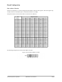
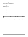
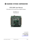
GPIO-MM-21 User Manual
FPGA-based PC/104 Digital I/O Module
User Manual v1.03
© Copyright 2010
1255 Terra Bella Ave.
Mountain View, CA 94043
Tel (650) 810-2500
Fax (650) 810-2525
www.diamondsystems.com
Table of Contents
General Description.........................................................................................................3
Overview....................................................................................................................3
Digital I/O Features....................................................................................................3
Board Layout....................................................................................................................4
Board Drawing...........................................................................................................4
I/O Connector Pinout.......................................................................................................5
Digital I/O Header Pinout...........................................................................................5
Auxiliary I/O Header Pinout........................................................................................6
Board Configuration........................................................................................................7
Base Address Selection.............................................................................................7
I/O Map..............................................................................................................................8
Register Bit Descriptions................................................................................................9
8255 Data Registers..................................................................................................9
8255 Control and Status Registers (Basic Mode Definition – MSFLAG=1)............10
8255 Control and Status Registers (Bit SET/RESET Mode – MSFLAG=0)............11
Programming Digital I/O................................................................................................12
Overview..................................................................................................................12
96-bit Programmable Direction (8255).....................................................................12
Specifications.................................................................................................................13
General Specifications.............................................................................................13
Additional Information..................................................................................................14
Datasheets...............................................................................................................14
Figures
Figure 1: GPIO-MM-21 Board Layout................................................................................4
Figure 2: Set 8255 Base Address to 0330h.......................................................................7
Diamond Systems Corporation
GPIO-MM-21 User Manual
Page 2
General Description
Overview
The GPIO-MM-21 is a PC/104 board featuring 96 Digital I/O (DIO) lines. The DIO function is implemented in
FPGA cores, emulating quad 82C55A PPI chips.
Two 50-pin I/O header provide for external DIO connections. Direction on all ports is selected by programming
control registers in the FPGA. 48 I/O lines are buffered with transceivers, whose directions are controlled by logic
that responds to the direction control values written to the registers. Each line is capable of sinking 64mA in a logic
low state or sourcing 15mA in a logic high state. The board requires only +5V for operation. The remaining 48 I/O
lines are capable of +/-24mA per line.
DIO headers are organized to allow direct interfacing to OPTO-22s isolated I/O racks, including the G4 series, the
PB16-H, -J, -K, -L, PB8H, and the PB24HQ. These racks and I/O modules allow up to 3000 VRMS isolation
between the computer and the user's signals. All control signals, power, and ground on the DIO header match the
corresponding signals on these I/O racks, so a single 50-pin ribbon cable, such as Diamond Systems' C50-18, is all
that is needed to make the connection.
Digital I/O Features
•
•
•
•
Quad 82C55A Parallel Peripheral Interfaces (PPI) logic implemented in FPGA cores.
Each 82C55A has three 8-bit I/O ports for a total of 96 DIO lines, which connect to two 50-pin headers for
external connections.
Port direction and operation is selected through software programmable control registers.
48 lines buffered with transceivers.
Diamond Systems Corporation
GPIO-MM-21 User Manual
Page 3
Board Layout
Board Drawing
Figure 1: GPIO-MM-21 Board Layout
Diamond Systems Corporation
GPIO-MM-21 User Manual
Page 4
I/O Connector Pinout
Digital I/O Header Pinout
Connectors J3 and J4 provide a total of 96 general-purpose DIO interfaces.
They can be pulled-up to +5V or pulled-down to ground using jumpers J8 and J11 respectively.
The following table shows the 82C55A port arrangement. Ports 1 and 2 are on connector J3 and ports 3 and 4 are on
connector J4.
J3
J4
Port 1A7
1
2
Port 2A7
Port 3A7
1
2
Port 4A7
Port 1A6
3
4
Port 2A6
Port 3A6
3
4
Port 4A6
Port 1A5
5
6
Port 2A5
Port 3A5
5
6
Port 4A5
Port 1A4
7
8
Port 2A4
Port 3A4
7
8
Port 4A4
Port 1A3
9
10
Port 2A3
Port 3A3
9
10
Port 4A3
Port 1A2
11
12
Port 2A2
Port 3A2
11
12
Port 4A2
Port 1A1
13
14
Port 2A1
Port 3A1
13
14
Port 4A1
Port 1A0
15
16
Port 2A0
Port 3A0
15
16
Port 4A0
Port 1B7
17
18
Port 2B7
Port 3B7
17
18
Port 4B7
Port 1B6
19
20
Port 2B6
Port 3B6
19
20
Port 4B6
Port 1B5
21
22
Port 2B5
Port 3B5
21
22
Port 4B5
Port 1B4
23
24
Port 2B4
Port 3B4
23
24
Port 4B4
Port 1B3
25
26
Port 2B3
Port 3B3
25
26
Port 4B3
Port 1B2
27
28
Port 2B2
Port 3B2
27
28
Port 4B2
Port 1B1
29
30
Port 2B1
Port 3B1
29
30
Port 4B1
Port 1B0
31
32
Port 2B0
Port 3B0
31
32
Port 4B0
Port 1C7
33
34
Port 2C7
Port 3C7
33
34
Port 4C7
Port 1C6
35
36
Port 2C6
Port 3C6
35
36
Port 4C6
Port 1C5
37
38
Port 2C5
Port 3C5
37
38
Port 4C5
Port 1C4
39
40
Port 2C4
Port 3C4
39
40
Port 4C4
Port 1C3
41
42
Port 2C3
Port 3C3
41
42
Port 4C3
Port 1C2
43
44
Port 2C2
Port 3C2
43
44
Port 4C2
Port 1C1
45
46
Port 2C1
Port 3C1
45
46
Port 4C1
Port 1C0
47
48
Port 2C0
Port 3C0
47
48
Port 4C0
+5V
49
50
Ground
+5V 49
50
Ground
NOTE: The connectors on the board are labeled “Port 1” and “Port 2” but do not denote the
82C55A port numbers shown here.
Diamond Systems Corporation
GPIO-MM-21 User Manual
Page 5
Signal
Description
Port 1A0-Port 1A7 8255-1 Port A, bits 0-7
Port 1B0-Port 1B7 8255-1 Port B, bits 0-7
Port 1C0-Port 1C7 8255-1 Port C, bits 0-7
Port 2A0-Port 2A7 8255-2 Port A, bits 0-7
Port 2B0-Port 2B7 8255-2 Port B, bits 0-7
Port 2C0-Port 2C7 8255-2 Port C, bits 0-7
Port 3A0-Port 3A7 8255-3 Port A, bits 0-7
Port 3B0-Port 3B7 8255-3 Port B, bits 0-7
Port 3C0-Port 3C7 8255-3 Port C, bits 0-7
Port 4A0-Port 4A7 8255-4 Port A, bits 0-7
Port 4B0-Port 4B7 8255-4 Port B, bits 0-7
Port 4C0-Port 4C7 8255-4 Port C, bits 0-7
+5V
Ground
+5 volt DC from the PC/104 bus.
Digital ground from the PC/104 bus.
Auxiliary I/O Header Pinout
The auxiliary I/O header (J5) is provided for bidirectional, TTL-level, general-purpose I/O.
1
AUXIO_0
2
AUXIO_1
3
AUXIO_2
4
AUXIO_3
5
GND
Card Voltage Type
Pin Configuration
AUXIO_0-AUXIO_3 Four bidirectional, TTL-level, general-purpose I/O signals.
GND
Diamond Systems Corporation
Ground
GPIO-MM-21 User Manual
Page 6
Board Configuration
Base Address Selection
Jumper J10, positions 4-9, is used to configure the base address of all four 8255 registers (The 8255 register map
occupies 16 bytes of I/O address space, as described in Section 5, I/O Map).
Jumper the locations as shown in the table to set the 8255 base addresses.
I/O
Address
0220h
0240h
0250h
0260h
0280h
0290h
02A0h
02B0h
02C0h
02D0h
02E0h
0300h
0330h
0340h
0350h
0360h
0380h
0390h
03A0h
03C0h
03E0h
9
Out
Out
Out
Out
Out
Out
Out
Out
Out
Out
Out
Out
Out
Out
Out
Out
Out
Out
Out
Out
Out
8
In
In
In
In
In
In
In
In
In
In
In
Out
Out
Out
Out
Out
Out
Out
Out
Out
Out
Jumper Position
7
6
In
In
In
Out
In
Out
In
Out
Out
In
Out
In
Out
In
Out
In
Out
Out
Out
Out
Out
Out
In
In
In
In
In
Out
In
Out
In
Out
Out
In
Out
In
Out
In
Out
Out
Out
Out
5
Out
In
In
Out
In
In
Out
Out
In
In
Out
In
Out
In
In
Out
In
In
Out
In
Out
4
In
In
Out
In
In
Out
In
Out
In
Out
In
In
Out
In
Out
In
In
Out
In
In
In
The following example selects an 8255 base address of 0330h.
Figure 2: Set 8255 Base Address to 0330h
Diamond Systems Corporation
GPIO-MM-21 User Manual
Page 7
I/O Map
Sixteen registers are used for DIO programming, as shown in the following table. The offsets shown in the table are
from the base address set using jumper J10, as described in the Board Configuration section.
Offset
00h
8255-1 port A DIO register
Description
01h
8255-1 port B DIO register
02h
8255-1 port C DIO register
03h
8255-1 control and status register
04h
8255-2 port A DIO register
05h
8255-2 port B DIO register
06h
8255-2 port C DIO register
07h
8255-2 control and status register
08h
8255-3 port A DIO register
09h
8255-3 port B DIO register
0Ah
8255-3 port C DIO register
0Bh
8255-3 control and status register
0Ch
8255-4 port A DIO register
0Dh
8255-4 port B DIO register
0Eh
8255-4 port C DIO register
0Fh
8255-4 control and status register
Diamond Systems Corporation
GPIO-MM-21 User Manual
Page 8
Register Bit Descriptions
Refer to the I/O Map section for the DIO register set list.
8255 Data Registers
DIO Base+00h (8255-1 Port A)
DIO Base+04h (8255-2 Port A)
DIO Base+08h (8255-3 Port A)
DIO Base+0Ch (8255-4 Port A)
DIO Base+01h (8255-1 Port B)
DIO Base+05h (8255-2 Port B)
DIO Base+09h (8255-3 Port B)
DIO Base+0Dh (8255-4 Port B)
DIO Base+02h (8255-1 Port C)
DIO Base+06h (8255-2 Port C)
DIO Base+0Ah (8255-3 Port C)
DIO Base+0Eh (8255-4 Port C)
Bit:
7
6
5
4
3
2
1
0
Name:
DATA
DATA
8-bit parallel data. On reset, the port is set to input mode and the port is held at a logic level 1 until the
reset signal is removed. The port remains in input mode until changed using the control register.
Following a reset, all lines are set to input mode.
Diamond Systems Corporation
GPIO-MM-21 User Manual
Page 9
8255 Control and Status Registers (Basic Mode Definition – MSFLAG=1)
DIO Base+03h (8255-1)
DIO Base+07h (8255-2)
DIO Base+0Bh (8255-3)
DIO Base+0Fh (8255-4)
Bit:
Name:
7
MSFLAG
6
5
MSELA
4
3
2
1
0
PADIR
PCUDIR
MSELB
PBDIR
PCLDIR
PCLDIR
Port C (lower) direction. Sets the direction of the port C I/O signals 0-3.
0 = output
1 = input ◄ (Reset value)
PBDIR
Port B direction. Sets the direction of the port B I/O signals.
0 = output
1 = input ◄ (Reset value)
MSELB
Group B mode selection. Sets the mode of operation for the group B signals.
0 = mode 0 ◄ (Reset value)
1 = mode 1
NOTE: 1. Only mode 0 is currently implemented.
2. All output registers are reset when the mode is changed.
PCUDIR
Port C (upper) direction. Sets the direction of the port C I/O signals 4-7.
0 = output
1 = input ◄ (Reset value)
PADIR
Port A direction Sets the direction of the port A I/O signals.
0 = output
1 = input ◄ (Reset value)
MSELA
Group A mode selection. Sets the mode of operation for the group B signals.
00h = mode 0 ◄ (Reset value)
01h = mode 1
1xh = mode
NOTE: 1. Only mode 0 is currently implemented.
2. All output registers are reset when the mode is changed.
MSFLAG
Mode set flag. Selects the port configuration mode.
0 = Bit set/reset control register mode
When MSFLAG is reset, this register is used to set/reset individual Port C bits.
1 = Basic mode definition control register mode ◄ (Reset value)
When MSFLAG is set, this register is used for direction and mode selection.
NOTE: When the control word is read, the value of MSFLAG is always 1, implying basic control
word information is being read.
Diamond Systems Corporation
GPIO-MM-21 User Manual
Page 10
8255 Control and Status Registers (Bit SET/RESET Mode – MSFLAG=0)
DIO Base+03h (8255-1)
DIO Base+07h (8255-2)
DIO Base+0Bh (8255-3)
DIO Base+0Fh (8255-4)
Bit:
Name:
7
MSFLAG
6
5
4
3
-
2
BSEL
1
0
SET
SET
Bit set/reset individual command.
0 = reset
1 = set
BSEL
Port C bit select.
0 = bit 0
1 = bit 1
2 = bit 2
3 = bit 3
4 = bit 4
5 = bit 5
6 = bit 6
7 = bit 7
MSFLAG
Mode set flag. Selects the port configuration mode.
0 = Bit set/reset control register mode
When MSFLAG is reset, this register is used to set/reset individual Port C
Bits.
1 = Basic mode definition control register mode
When MSFLAG is set, this register is used for direction and mode selection.
NOTE: When the control word is read, the value of MSFLAG is always 1, implying basic control
word information is being read.
Diamond Systems Corporation
GPIO-MM-21 User Manual
Page 11
Programming Digital I/O
Overview
GPIO-MM-21 provides 96 DIO lines using an FPGA core implementation of four 8255 devices (8255-1, 8255-2,
8255-3 and 8255-4). All I/O lines contain jumper-selectable 10KΩ pull-up/pull-down resistors.
96-bit Programmable Direction (8255)
Operation of the 8255 FPGA core should be as described in the 8255 PPI datasheet. Refer to the 8255 datasheet,
Additional Information, for detailed register and programming information.
The 8255 has three parallel I/O ports. Ports A and B are 8-bit bi-directional I/O ports. Port C is divided into two 4bit bi-directional I/O ports. For programming, the ports are arranged into two groups, as shown below.
Port Group
A
B
Description
8 bits of Port A and upper 4 bits (4-7) of port C.
8 bits of Port B and lower 4 bits (0-3) of port C.
NOTE: The port groups can be separately configured for different operating modes. However,
GPIO-MM-21 only implements operating mode 0, which provides simple, bidirectional I/O without
handshaking.
Port C bits may be individually set and reset by setting the MSFLAG in the 8255 Control and Status Register and
programming the remaining register bits for the desired bit state.
Setting the 8255 Control and Status Register to the following values gives 16 possible I/O configurations.
Status and Control Register Bits
PADIR PCUDIR PBDIR PCLDIR
Group A
Port A
Port C
(upper)
Group B
Port B
Port C
(lower)
0
0
0
0
Output
Output
Output
Output
0
0
0
1
Output
Output
Output
Input
0
0
1
0
Output
Output
Input
Output
0
0
1
1
Output
Output
Input
Input
0
1
0
0
Output
Input
Output
Output
0
1
0
1
Output
Input
Output
Input
0
1
1
0
Output
Input
Input
Output
0
1
1
1
Output
Input
Input
Input
1
0
0
0
Input
Output
Output
Output
1
0
0
1
Input
Output
Output
Input
1
0
1
0
Input
Output
Input
Output
1
0
1
1
Input
Output
Input
Input
1
1
0
0
Input
Input
Output
Output
1
1
0
1
Input
Input
Output
Input
1
1
1
0
Input
Input
Input
Output
1
1
1
1
Input
Input
Input
Input
Diamond Systems Corporation
GPIO-MM-21 User Manual
Page 12
Specifications
General Specifications
•
•
•
•
•
•
•
•
•
•
•
Base FPGA: Xilinx Spartan II, 200,000 gates, 40K RAM bits
Input clock: 40MHz
FPGA code storage: Flash memory, field upgradeable via JTAG
ID indicator: 8-bit LED display indicates FPGA code personality; field upgradeable via JTAG
Programmable I/O: 96, using 2 82C55A cores
Output current:
• Port 1 unbuffered I/O: +/-24mA per line
• Port 2 buffered I/O: Logic 0: 64mA max per line, Logic 1: -15mA max per line
Dimensions: 3.55" x 3.775", PC/104 form factor
PC/104 bus: 16-bit stackthrough ISA bus
Power supply: +5VDC ±5%
Operating temperature: -40° to +85° C
Weight: 2.2oz
Diamond Systems Corporation
GPIO-MM-21 User Manual
Page 13
Additional Information
Datasheets
Datasheets provide programming reference information for the DIO functions.
1. 82C55A CMOS Programmable Peripheral Interface , Harris Semiconductor, March 1997
Diamond Systems Corporation
GPIO-MM-21 User Manual
Page 14