1
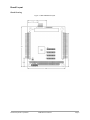
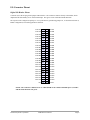
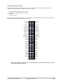
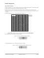
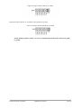
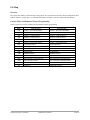
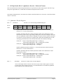
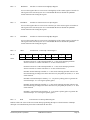
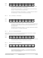
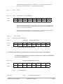
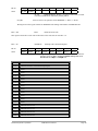
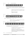
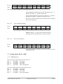
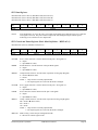
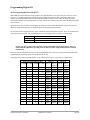
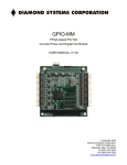
GPIO-MM User Manual
FPGA-based PC/104 Counter/Timer and Digital I/O Module
User Manual v1.0
Personality 0x22
© Copyright 2006
1255 Terra Bella Ave.
Mountain View, CA 94043
Tel (650) 810-2500
Fax (650) 810-2525
www.diamondsystems.com
Diamond Systems Corporation
GPIO-MM User Manual
Page 1
Table of Contents
General Description.........................................................................................................4
Overview....................................................................................................................4
Digital I/O Features....................................................................................................4
Counter/Timer Features.............................................................................................4
Enhanced Features....................................................................................................5
Board Layout....................................................................................................................5
Board Drawing...........................................................................................................5
I/O Connector Pinout.......................................................................................................6
Digital I/O Header Pinout...........................................................................................7
Counter/timer Header Pinout.....................................................................................8
Auxiliary I/O Header Pinout........................................................................................9
Board Configuration......................................................................................................10
Base Address Selection...........................................................................................11
Interrupt Level Selection..........................................................................................11
I/O Line Pull-up/Pull-down Selection....................................................................... 12
I/O Map............................................................................................................................13
Overview..................................................................................................................14
Counter/Timer and Enhanced Feature Programming............................................. 14
DIO Programming....................................................................................................15
Register Bit Descriptions..............................................................................................16
9513 Command and Status Data ........................................................................... 16
9513 Command and Status Data Pointer Registers................................................16
9513 DIO Data Registers.........................................................................................16
9513 Interrupt Control Registers..............................................................................17
EEPROM Data Register..........................................................................................17
EEPROM Address Register.....................................................................................17
EEPROM Control and Status Register....................................................................18
FPGA Revision Code Register................................................................................18
Interrupt Source Register.........................................................................................19
Interrupt Control and Status Register......................................................................20
Auxiliary DIO Control and Status Register...............................................................20
Board Reset and ID Register...................................................................................21
8255 Data Registers................................................................................................21
8255 Control and Status Registers (Basic Mode Definition – MSFLAG=1)............ 22
8255 Control and Status Registers (Bit SET/RESET Mode – MSFLAG=0)............23
Quadrature Encoder and External Interrupts............................................................. 24
Diamond Systems Corporation
GPIO-MM User Manual
Page 2
Programming the Counter/Timer.................................................................................24
Overview..................................................................................................................24
Accessing the Counter/Timer Internal Registers.....................................................24
Master Mode Register..............................................................................................24
Counter Mode Register............................................................................................24
Counter Modes.........................................................................................................24
FOUT Frequency Output.........................................................................................24
Counter Commands.................................................................................................24
Counter Programming..............................................................................................25
Programming Digital I/O................................................................................................25
48-bit Programmable Direction (8255).....................................................................25
16-bit Fixed Direction (9513)....................................................................................25
Programming Enhanced Features...............................................................................26
EEPROM Programming...........................................................................................26
Specifications.................................................................................................................26
General Specifications.............................................................................................26
Additional Information..................................................................................................27
Datasheets...............................................................................................................27
Technical Support..........................................................................................................27
Figures
Figure 1: GPIO-MM Board Layout.....................................................................................6
Figure 2: Example - Set DIO Base Address to 0040h.....................................................11
Figure 3: Example - Set Counter/Timer Base Address to 0100h....................................11
Figure 4: Example - Route IRQA to PC/104 IRQ5.......................................................... 12
Figure 5: Example - Connect IRQA to Pull-down Resistor and Route to Shared IRQ5..12
Figure 6: Example - Pull I/O Pins Up to +5VDC..............................................................13
Figure 7: Example - Pull I/O Pins Down to Ground.........................................................13
Diamond Systems Corporation
GPIO-MM User Manual
Page 3
General Description
Overview
The GPIO-MM is a PC/104 board featuring 48 Digital I/O (DIO) lines, 2 dual input quadrature encoders, 14 external
interrupt lines and software-controlled interrupt capability. The DIO and quadrature encoders functions are
implemented in FPGA cores, emulating dual 82C55A PPI and dual Avago HCTL-2001 encoder chips.
A 50-pin I/O header provides for external DIO connections. Direction on all ports is selected by programming
control registers in the FPGA. All I/O lines are buffered with transceivers, whose directions are controlled by logic
that responds to the direction control values written to the registers. Each line is capable of sinking 64mA in a logic
low state or sourcing 15mA in a logic high state. The board requires only +5V for operation.
DIO headers are organized to allow direct interfacing to OPTO-22s isolated I/O racks, including the G4 series, the
PB16-H, -J, -K, -L, PB8H, and the PB24HQ. These racks and I/O modules allow up to 3000 VRMS isolation
between the computer and the user's signals. All control signals, power, and ground on the DIO header match the
corresponding signals on these I/O racks, so a single 50-pin ribbon cable, such as Diamond Systems' C50-18, is all
that is needed to make the connection.
The GPIO-MM provides access to interrupt levels 3-7, 10-12 and 15 on the PC bus for real-time background
applications. Interrupts provide a means for transferring data into or out of PC memory under external control.
Using interrupts allows "background" operation, where I/O can be performed while the PC is executing another task
, such as running an unrelated applications program. This feature is useful for performing I/O at a controlled rate,
since a counter output can be used to drive the interrupt request pin on the I/O header at a periodic rate for a usersupplied interrupt service routine that performs whatever function is necessary in response to the interrupt.
Digital I/O Features
•
•
•
•
Dual 82C55A Parallel Peripheral Interfaces (PPI) logic implemented in FPGA cores.
Each 82C55A has three 8-bit I/O ports for a total of 48 DIO lines, which connect to a 50-pin header for external
connections.
Port direction and operation is selected through software programmable control registers.
All lines are buffered with transceivers.
Two Quadrature Position Encoders
•
•
•
•
Encoder inputs are rising/falling edge selectable
Each encoder is individually enabled/disabled
Each encoder is followed by a 16 bit counter
Each 16 bit counter is presettable to any 16 bit value
Interrupt Features
•
•
•
•
16 multiplexed encoder interrupt sources, 1 from each counter (below) and 14 External Interrupt lines are
multiplexed onto a single PC104 IRQ output line
All interrupt sources are rising/falling edge selectable
All interrupt sources are individually enabled/disabled
All int sources
Enhanced Features
•
•
•
•
•
On-board EEPROM for user configuration data storage.
An LED display for easy identification of FPGA personality, which can also be read in a register.
Interrupt source selection, with counter/timer, DIO or external line options.
A register-accessible FPGA revision code for version control.
Software-controlled board reset.
Diamond Systems Corporation
GPIO-MM User Manual
Page 4
Board Layout
Board Drawing
Figure 1: GPIO-MM Board Layout
Diamond Systems Corporation
GPIO-MM User Manual
Page 5
I/O Connector Pinout
Digital I/O Header Pinout
Connector (J4) is the 50-pin general-purpose DIO interface. The connector connects directly to the FPGA, which
implements the functionality of two 82C55A PPI chips. This gives a total of 48 bidirectional DIO lines.
The J4 pins can be configured to pull-up to +5V or pull-down to ground using jumper J11, as described in Section 4,
Board Configuration, Line Pull-up/pull-down Selection.
Port 1A7
1
2
Port 2A7
Port 1A6
3
4
Port 2A6
Port 1A5
5
6
Port 2A5
Port 1A4
7
8
Port 2A4
Port 1A3
9
10
Port 2A3
Port 1A2
11
12
Port 2A2
Port 1A1
13
14
Port 2A1
Port 1A0
15
16
Port 2A0
Port 1B7
17
18
Port 2B7
Port 1B6
19
20
Port 2B6
Port 1B5
21
22
Port 2B5
Port 1B4
23
24
Port 2B4
Port 1B3
25
26
Port 2B3
Port 1B2
27
28
Port 2B2
Port 1B1
29
30
Port 2B1
Port 1B0
31
32
Port 2B0
Port 1C7
33
34
Port 2C7
Port 1C6
35
36
Port 2C6
Port 1C5
37
38
Port 2C5
Port 1C4
39
40
Port 2C4
Port 1C3
41
42
Port 2C3
Port 1C2
43
44
Port 2C2
Port 1C1
45
46
Port 2C1
Port 1C0
47
48
Port 2C0
+5V
49
50
Ground
NOTE: The connector is labeled “Port 2,” which should not be confused with DIO ports A, B and C
and the fixed-direction TTL ports.
Diamond Systems Corporation
GPIO-MM User Manual
Page 6
Signal
Description
Port 1A0-Port 1A7 8255-1 Port A, bits 0-7
Port 1B0-Port 1B7 8255-1 Port B, bits 0-7
Port 1C0-Port 1C7 8255-1 Port C, bits 0-7
Port 2A0-Port 2A7 8255-2 Port A, bits 0-7
Port 2B0-Port 2B7 8255-2 Port B, bits 0-7
Port 2C0-Port 2C7 8255-2 Port C, bits 0-7
+5V
Ground
Diamond Systems Corporation
+5 volt DC from the PC/104 bus.
Digital ground from the PC/104 bus.
GPIO-MM User Manual
Page 7
Counter/timer Header Pinout
Connector (J3) is the 50-pin counter/timer interface. The connector connects directly to the FPGA, which
implements the functionality of two CTS9513 counter/timer chips.
•
•
•
•
Ten input and ten output counter/timer signals
Eight input and eight output TTL-level signals
Ten gates
Power and ground
The J3 pins may be configured to pull-up to +5V or pull-down to ground using jumper J8, as describe in Section 4,
Board Configuration, Line Pull-up/pull-down Selection.
Q_In_1_A
1
2
Q_In_1_B
Unused
3
4
Unused
Q_In_2_A
5
6
Q_In_2_B
Unused
7
8
Unused
Ext_IRQ_1
9
10
Ext_IRQ_2
Ext_IRQ_3
11
12
Ext_IRQ_4
Ext_IRQ_5
13
14
Ext_IRQ_6
Ext_IRQ_7
15
16
Ext_IRQ_8
Ext_IRQ_9
17
18
Ext_IRQ_10
Ext_IRQ_11
19
20
Ext_IRQ_12
Ext_IRQ_13
21
22
Ext_IRQ_14
Unused
23
24
Unused
Unused
25
26
Unused
Unused
27
28
Unused
Unused
29
30
Unused
Unused
31
32
Unused
Unused
33
34
Unused
Unused
35
36
Unused
Unused
37
38
Unused
Unused
39
40
Unused
Unused
41
42
Unused
Unused
43
44
Unused
Unused
45
46
Unused
Unused
47
48
Unused
+5V
49
50
Ground
NOTE: The connector is labeled “Port 1,” which should not be confused with DIO ports A, B and C
and the fixed-direction TTL ports.
Diamond Systems Corporation
GPIO-MM User Manual
Page 8
Signal
Q_In_1_<A:B>
Description
Are the A and B inputs of Quadrature Encoder 1 and are
standard TTL input lines.
Q_In_2_<A:B>
Are the A and B inputs of Quadrature Encoder 2 and are the
standard TTL input lines.
Ext_IRQ_<1:14>
Are dedicated interrupt input lines and can be selected as a
source for IRQ trigger.
+5V
Ground
+5 volt DC from the PC/104 bus.
Digital ground from the PC/104 bus.
Auxiliary I/O Header Pinout
The auxiliary I/O header (J5) is provided for bidirectional, TTL-level, general-purpose I/O.
1
AUXIO_0
2
AUXIO_1
3
AUXIO_2
4
AUXIO_3
5
GND
Card Voltage Type
Pin Configuration
AUXIO_0-AUXIO_3 Four bidirectional, TTL-level, general-purpose I/O signals.
GND
Diamond Systems Corporation
Ground
GPIO-MM User Manual
Page 9
Board Configuration
Base Address Selection
Jumper J10, positions 2-5, is used to configure the base address of the DIO (8255) registers. The 8255 register map
occupies 8 bytes of I/O address space, as described in Section 5, I/O Map.
Jumper positions 6-9, is used to configure the base address of the counter/timer I/O (9513) registers and the
enhanced features registers. The 9513 register map occupies 16 bytes of I/O address space, as described in Section
5, I/O Map.
Jumper the locations as shown to set the 8255 and 9513 base addresses.
I/O
Address
0040h
0080h
00C0h
0100h
0140h
0180h
01C0h
0200h
0240h
0280h
02C0h
0300h
0340h
0380h
03C0h
2
6
Out
In
Out
In
Out
In
Out
In
Out
In
Out
In
Out
In
Out
3
7
In
Out
Out
In
In
Out
Out
In
In
Out
Out
In
In
Out
Out
4
8
In
In
In
Out
Out
Out
Out
In
In
In
In
Out
Out
Out
Out
5
9
In
In
In
In
In
In
In
Out
Out
Out
Out
Out
Out
Out
Out
◄ DIO Pins
◄ C/T Pins
NOTE: Different address must be selected for the DIO and counter/timer functions.
The example, below, selects a DIO base address of 0040h.
Figure 2: Example - Set DIO Base Address to 0040h
The following example selects a counter/timer base address of 0100h.
Figure 3: Example - Set Counter/Timer Base Address to 0100h
Diamond Systems Corporation
GPIO-MM User Manual
Page 10
Interrupt Level Selection
Jumper J7 is used to switch the IRQA interrupt and jumper J9 is used to switch the IRQB interrupt. PC/104 lines
that can be selected are IRQ3 to IRQ7, IRQ10 to IRQ12 and IRQ15. (The examples shown below also apply to the
J9 jumper block for IRQB).
The example, below, shows J7 jumpered to route IRQA to PC/104 IRQ5.
Figure 4: Example - Route IRQA to PC/104 IRQ5
Jumper blocks J7 and J9 are also used to enable interrupt sharing for each IRQ signal, enabling a 1K Ohm pull-down
resistor.
When an I/O module drives an IRQ line, its output signal must either drive logic high, or become a tri-state input.
This allows more than one device to be on a single IRQ line. To facilitate this, a pull-down resistor is used on the
IRQ line to bring the logic low when no device is signaling an interrupt. Shorting the “R,” resistor, jumper connects
a 1K pull-down resistor between the IRQ line and ground.
The following example shows IRQA connected to a 1K pull-down resistor and routed to IRQ5, which is shared.
Figure 5: Example - Connect IRQA to Pull-down Resistor and Route to
Shared IRQ5
NOTE: There can only be one pull-down resistor per IRQ line. If jumper blocks J7 and J9 both
select IRQ5, only one jumper block should have the R-jumper inserted. Likewise, there should only
be one R-jumper in a configuration of multiple GPIO-MM boards.
NOTE: All positions are paralleled with zero-ohm resistor locations for hard-wire configuration.
IRQA and IRQB interrupts sources are selected by configuring the enhanced feature register, 0Ch, as described in
the Section 6, Register Bit Descriptions, Interrupt Source Register.
NOTE: All positions are paralleled with zero-ohm resistor locations for hard-wire configuration line
pull-up/pull-down selection.
I/O Line Pull-up/Pull-down Selection
Use jumper J8 to configure the pull-up and pull-down state of the counter/timer header pins (J3). Use jumper J11 to
configure the pull-up and pull-down state of the DIO header pins (J4).
DIO pin pull-up and pull-down state is configured as shown in the following examples.
Jumper the position marked “+5” to pull the J3 I/O pins up to +5VDC.
Diamond Systems Corporation
GPIO-MM User Manual
Page 11
Figure 6: Example - Pull I/O Pins Up to +5VDC
Jumper the position marked “G” to pull the J3 I/O pins down to ground.
Figure 7: Example - Pull I/O Pins Down to Ground
NOTE: Placing a jumper on both “+5” and “G” simultaneously will short the +5VDC power plane
to ground.
Diamond Systems Corporation
GPIO-MM User Manual
Page 12
I/O Map
Overview
The register base address is determined by setting jumper J10, as described in Section 4, Board Configuration, Base
Address Selection. Jumper pins 2-5 set the DIO base address and pins 6-9 set the counter/timer base address.
Counter/Timer and Enhanced Feature Programming
Sixteen registers are used for counter/timer and enhanced feature programming.
Offset
00h
Write Function
Encoder 1 & 2 Control Settings
Read Function
Encoder 1 & 2 Control Readback
01h
Encoder 1 Counter low byte
Encoder 1 Counter low byte
02h
Encoder 1 Counter high byte
Encoder 1 Counter high byte
03h
Encoder 2 Counter low byte
Encoder 2 Counter low byte
04h
Encoder 2 Counter high byte
Encoder 2 Counter high byte
05h
Encoder + Ext interrupt control
Encoder + Ext interrupt status
06h
Ext interrupt control
Ext interrupt status
07h
Ext interrupt control
08h
Ext interrupt control
09h
EEPROM Data
EEPROM Data
0Ah
EEPROM Address
EEPROM Address
0Bh
EEPROM Control
FPGA Revision
0Ch
Master Interrupt Circuit Selection
Master Interrupt Circuit Read-back
0Dh
Master Interrupt Control
Master Interrupt & EEPROM Status
0Eh
Auxiliary DIO Control
Auxiliary DIO Read-back
0Fh
Board Reset
Board ID Read-back
Diamond Systems Corporation
GPIO-MM User Manual
Page 13
1.1
I/O Map Details, Block 1: Quadrature Encoder + Enhanced Features
This section describes the location and general behavior of specific bits in each I/O map register. This does not go
into specific signal behavior, for which there are detailed descriptions in future sections.
In all register definitions below, a bit named X (or blank) is not defined and serves no function. Unused bits should
return ‘0’ when read.
1.1.1 Quadrature Encoder Registers
Base + 0
Read/Write
Bit No.
7
Name
Encoder 1 & 2 Control Setting & Readback Register
6
5
QE1EN QE1POL
4
3
2
QE2EN
QE2POL
1
0
QE1EN: Quadrature Encoder #1 Enable. A ‘1’ turns on the Encoder/Counter function for
Encoder #1. A ‘0’ turns off the function.
QE1POL: Quadrature Encoder #1 Polarity determines under what conditions the counter
increments up or down. Every edge (rising or falling) on A or B causes a change in the count.
Not every quadrature encoder defines A leading B as Counter Clockwise rotation (sometimes
it's Clockwise). So, the polarity bit is typically used to define the relationship between A/B,
counting up, and the direction of the encoder shaft rotation. We define the following:
Polarity bit = 1: Input A edge leading input B edge = counting up,
Input B edge leading input A edge = counting down. (default)
Polarity bit = 0: Input A edge leading B edge = counting down,
Input B edge leading A edge = counting up.
QE2EN: Quadrature Encoder #2 Enable. A ‘1’ turns on the Encoder/Counter function for
Encoder #2. A ‘0’ turns off the function.
QE2POL: Quadrature Encoder #2 Polarity determines under what conditions the counter
increments up or down.
Polarity bit = 1: Input A edge leading input B edge = counting up,
Input B edge leading input A edge = counting down. (default)
Polarity bit = 0: Input A edge leading B edge = counting down,
Input B edge leading A edge = counting up.
Base + 1
Read/Write
Encoder #1 Counter Preset Low-Byte Register
Access to this register allows a read or write to the low byte of the counter register of encoder
#1. This register can be read at any time. It is recommended that the user disable the quadrature
encoder function while writing this register.
Diamond Systems Corporation
GPIO-MM User Manual
Page 14
Base + 2
Read/Write
Encoder #1 Counter Preset High-Byte Register
Access to this register allows a read or write to the high byte of the counter register of encoder #1.
This register can be read at any time. It is recommended that the user disable the quadrature
encoder function while writing this register.
Base + 3
Read/Write
Encoder #2 Counter Preset Low-Byte Register
Access to this register allows a read or write to the low byte of the counter register of encoder #2.
This register can be read at any time. It is recommended that the user disable the quadrature
encoder function while writing this register.
Base + 4
Read/Write
Encoder #2 Counter Preset High-Byte Register
Access to this register allows a read or write to the high byte of the counter register of encoder #2.
This register can be read at any time. It is recommended that the user disable the quadrature
encoder function while writing this register.
Base + 5
Write
Bit No.
7
Name
E1CIEN
Encoder/EXT 1-2 Interrupt Control Register
6
5
E2CIEN
4
3
2
1
0
EXI1EN EXI1POL EXI2EN EXI2POL
E1CIEN: Encoder #1 Counter Interrupt Enable. A ‘1’ turns on the interrupt generation
whenever Encoder #1 Counter increments. A ‘0’ turns off the function.
E2CIEN: Encoder #2 Counter Interrupt Enable. A ‘1’ turns on the interrupt generation
whenever Encoder #2 Counter increments. A ‘0’ turns off the function.
EXI1EN: External Interrupt #1 Enable. A ‘1’ turns on the interrupt generation whenever the
External interrupt pin changes state in the direction set by the polarity bit (below). A ‘0’ turns
off the function.
EXI1POL: External Interrupt #1 Polarity. A ‘1’ sets positive polarity pulses to generate the
external interrupt. A ‘0’ sets negative polarity pulses
EXI2EN: External Interrupt #2 Enable. A ‘1’ turns on the interrupt generation whenever the
External interrupt pin changes state in the direction set by the polarity bit (below). A ‘0’ turns
off the function.
EXI2POL: External Interrupt #2 Polarity. A ‘1’ sets positive polarity pulses to generate the
external interrupt. A ‘0’ sets negative polarity pulses
Base + 5
Read
Encoder/EXT 1-6 Interrupt Status Register
Indicates what is the source of the most current interrupt generating Interrupt A to the PC104 Bus. If multiple
interrupts occur simultaneously then all are indicated at the same time.
Diamond Systems Corporation
GPIO-MM User Manual
Page 15
Bit No.
7
6
5
4
3
2
1
0
Name
E1CIST
E2CIST
EXI1ST
EXI2ST
EXI3ST
EXI4ST
EX5ST
EXI6ST
E1CIST: Encoder #1 Interrupt Status. A ‘1’ means this counter was a source of the current
interrupt. A ‘0’ means it was not involved in the interrupt.
E2CIST: Encoder #2 Interrupt Status. A ‘1’ means this counter was a source of the current
interrupt. A ‘0’ means it was not involved in the interrupt.
EXI[1:6]ST: External Interrupt #1 Interrupt Status. A ‘1’ means this counter was a source of
the current interrupt. A ‘0’ means it was not involved in the interrupt.
Base + 6
Bit No.
Name
Write
EXT Interrupt 3-6 Control Register
7
6
5
4
3
2
1
0
EXI3EN EXI3POL EXI4EN EXI4POL EXI5EN EXI5POL EXI6EN EXI6POL
EXI[3:6]EN: External Interrupt #3-6 Enable. A ‘1’ turns on the interrupt generation whenever
the External interrupt pin changes state in the direction set by the polarity bit (below). A ‘0’
turns off the function.
EXI[3:6]POL: External Interrupt #3-6 Polarity. A ‘1’ sets positive polarity pulses to generate
the external interrupt. A ‘0’ sets negative polarity pulses
Base + 6
Read
EXT 7-14 Interrupt Status Register
Indicates what is the source of the most current interrupt generating Interrupt A to the PC104 Bus. If multiple
interrupts occur simultaneously then all are indicated at the same time.
Bit No.
7
6
Name
EXI7ST
EXI8ST
5
4
3
2
1
0
EXI9ST EXI10ST EXI11ST EXI12ST EXI13ST EXI14ST
EXI[7:14]ST: External Interrupt #7-14 Interrupt Status. A ‘1’ means this counter was a source
of the current interrupt. A ‘0’ means it was not involved in the interrupt.
Base + 7
Bit No.
Name
Write EXT Interrupt 7-10 Control Register
7
6
5
4
3
2
1
0
EXI7EN EXI7POL EXI8EN EXI8POL EXI9EN EXI9POL EXI10EN EXI10POL
EXI[7:10]EN External Interrupt #7-10 Enable. A ‘1’ turns on the interrupt generation
whenever the External interrupt pin changes state in the direction set by the polarity bit
(below). A ‘0’ turns off the function.
Diamond Systems Corporation
GPIO-MM User Manual
Page 16
EXI[7:10]POL: External Interrupt #7-10 Polarity. A ‘1’ sets positive polarity pulses to
generate the external interrupt. A ‘0’ sets negative polarity pulses
Base + 7
Read
Unused
Base + 8
Write
EXT Interrupt 11-14 Control Register
Bit No.
7
6
5
4
3
2
1
0
EXI11EN EXI11POL EXI12EN EXI12POL EXI13EN EXI13POL EXI14EN EXI14POL
Name
EXI[11:14]EN: External Interrupt #11-14 Enable. A ‘1’ turns on the interrupt generation
whenever the External interrupt pin changes state in the direction set by the polarity bit
(below). A ‘0’ turns off the function.
EXI[11:14]POL: External Interrupt #11-14 Polarity. A ‘1’ sets positive polarity pulses to
generate the external interrupt. A ‘0’ sets negative polarity pulses
Base + 8
Read Unused
1.1.2
Enhanced Feature Registers
Base + 9
Read/Write
EEPROM Data Register
Bit No.
7
6
5
4
3
2
1
0
Name
D7
D6
D5
D4
D3
D2
D1
D0
D7-0
Data to be read or written to the EEPROM
For EEPROM write operations, the data written to this register will be written to the EEPROM.
For EEPROM read operations, this register contains the data read from the EEPROM
and is valid after EEBUSY = 0.
Base + 0A
Read/Write EEPROM Address Register
Bit No.
7
6
5
4
3
2
1
0
Name
A7
A6
A5
A4
A3
A2
A1
A0
A7-A0
EEPROM address.
Base + 0B
Diamond Systems Corporation
Write
EEPROM Control Register
GPIO-MM User Manual
Page 17
Bit No.
7
6
Name
EE_EN
EE_RW
5
4
3
2
1
0
EE_EN
EEPROM Enable. Writing a 1 to this bit will initiate a transfer
to/from the EEPROM as indicated by the EE_RW bit.
EE_RW
Selects read or write operation for the EEPROM: 0 = Write, 1 = Read.
Writing 0xC0 to this register initiates an EEPROM read. Writing 0x80 initiates an EEPROM write.
Base + 0B
Read
FPGA Revision Code
This register returns the revision code of the FPGA. This code starts at 0x10=Rev 1.0.
Base + 0C
Read/Write
Interrupt Source Selection Register
Bit No.
7
6
5
4
3
2
1
0
Name
IRQB3
IRQB2
IRQB1
IRQB0
IRQA3
IRQA2
IRQA1
IRQA0
IRQ[B:A][3:0]: Forms a 4-bit value from 0 to 15 that determines the
interrupt source for IRQA and IRQB. Defaults after power-on or
board reset are: IRQA = 0, IRQB = 12
Value
Source
0
Quadrature Encoders / External Interrupt Inputs
1
Unused
2
Unused
3
Unused
4
Unused
5
Unused
6
Unused
7
Unused
8
Unused
9
Unused
10
Unused
11
Unused
12
GMM-side 8255 #1 C0
13
GMM-side 8255 #1 C3
14
GMM-side 8255 #2 C0
15
GMM-side 8255 #2 C3
Diamond Systems Corporation
GPIO-MM User Manual
Page 18
Base + OD
Write
Bit No.
7
6
Interrupt Control Register
5
4
3
2
IRQBEN IRQBDIS IRQBCLR
Name
1
0
IRQAEN IRQADIS IRQACLR
This is a command register. Commands are issued by writing a ‘1’ to specific bits. More than one
bit can be written to at a time. If both enable and disable are called simultaneously, the IRQ will
be disabled.
IRQ[B:A]CLR: Clears the interrupt flip-flop for IRQ[B:A]. This must
called each time IRQ[B:A] occurs to reset the output state of the IRQ
line.
IRQ[B:A]DIS: Disable IRQ[B:A].
IRQ[B:A]EN: Enable IRQ[B:A].
Base + 0D
Read
Bit No.
7
Master Interrupt & EEPROM Status Register
6
5
Name
4
3
2
1
EEBUSY IRQBSTS
EEBUSY
0
IRQASTS
EEPROM busy indicator: ‘0’ = not busy, ‘1’ = busy
IRQ[B:A]STS: Reads back as a ‘1’ if that IRQ has triggered. This can only be
cleared to ‘0’ by issuing a IRQ[B:A]RST command.
Base + 0E
Bit No.
Name
Write
7
Auxiliary DIO Control Register
6
5
4
3
2
1
0
AUX3DIR AUX2DIR AUX1DIR AUX0DIR AUX3OUT AUX2OUT AUX1OUT AUX0OUT
This register is used to change the input/output state and the output levels of the auxiliary DIO
lines. All output levels are set to ‘0’ (low) on power-on or reset.
AUX[3:0]DIR: Sets the direction for each auxiliary line. Writing a ‘1’
sets input mode, writing a ‘0’ sets output mode.
All I/O states are set to ‘1’ (input) at power-on or reset.
AUX[3:0]OUT: Sets the output level for each line. Writing a ‘1’ sets
output high, writing a ‘0’ sets output low. These bits are valid even if
the port is currently in input mode, and will determine the output level
if the port is set to output mode.
Base + 0E
Read Interrupt Status Register
Diamond Systems Corporation
GPIO-MM User Manual
Page 19
Bit No.
Name
7
6
5
4
3
2
1
0
AUX3DIR AUX2DIR AUX1DIR AUX0DIR AUX3IN AUX2IN AUX1IN AUX0IN
This register is used to read the state of the auxiliary DIO lines.
AUX[3:0]DIR: Reads back the direction for each auxiliary line. A ‘1’
indicates input mode, a ‘0’ indicates output mode.
AUX[3:0]IN: Reads back the input level for each line. A ‘1’ indicates
the input level is high, a ‘0’ indicates the input level is low.
If the port is currently in output mode, the read-back value corresponds
to the current output level.
Base + 0F
Bit No.
Write Board Reset Register
7
6
5
4
3
2
1
Name
0
BRDRST
BRDRST: Writing a ‘1’ to this register initiates a board reset,
performing the same initialization as an external reset pulse.
Base + 0F
Read ID Code Register
Bit No.
7
6
5
4
3
2
1
0
Name
ID7
ID6
ID5
ID4
ID3
ID2
ID1
ID0
ID[7:0]: Reads back the personality ID code for this FPGA. The value
is hardcoded as 0x22.
1.2 I/O Map Details, Block 2: GMM
1.2.1 GMM Registers
These four registers map directly to the first 8255 core.
Base + 0
Read/Write
Port A Data
Base + 1
Read/Write
Port B Data
Base + 2
Read/Write
Port C Data
Base + 3
Read/Write
DIO Control Register
These four registers map directly to the second 8255 core.
Base + 4
Read/Write
Port A Data
Base + 5
Read/Write
Port B Data
Base + 6
Read/Write
Port C Data
Base + 7
Read/Write
DIO Control Register
Diamond Systems Corporation
GPIO-MM User Manual
Page 20
8255 Data Registers
DIO Base+00h (8255-1 Port A), DIO Base+04h (8255-2 Port A)
DIO Base+01h (8255-1 Port B), DIO Base+05h (8255-2 Port B)
DIO Base+02h (8255-1 Port C), DIO Base+06h (8255-2 Port C)
Bit:
7
6
5
4
3
2
1
0
Name:
DATA
DATA
8-bit parallel data. On reset, the port is set to input mode and the port is held at a logic level 1 until the
reset signal is removed. The port remains in input mode until changed using the control register.
Following a reset, all lines are set to input mode.
8255 Control and Status Registers (Basic Mode Definition – MSFLAG=1)
DIO Base+03h (8255-1), DIO Base+07h (8255-2)
Bit:
Name:
7
MSFLAG
6
5
MSELA
4
3
2
1
0
PADIR
PCUDIR
MSELB
PBDIR
PCLDIR
PCLDIR
Port C (lower) direction. Sets the direction of the port C I/O signals 0-3.
0 = output
1 = input ◄ (Reset value)
PBDIR
Port B direction. Sets the direction of the port B I/O signals.
0 = output
1 = input ◄ (Reset value)
MSELB
Group B mode selection. Sets the mode of operation for the group B signals.
0 = mode 0 ◄ (Reset value)
1 = mode 1
NOTE: 1. Only mode 0 is currently implemented.
2. All output registers are reset when the mode is changed.
PCUDIR
Port C (upper) direction. Sets the direction of the port C I/O signals 4-7.
0 = output
1 = input ◄ (Reset value)
PADIR
Port A direction Sets the direction of the port A I/O signals.
0 = output
1 = input ◄ (Reset value)
MSELA
Group A mode selection. Sets the mode of operation for the group B signals.
00h = mode 0 ◄ (Reset value)
01h = mode 1
1xh = mode
NOTE: 1. Only mode 0 is currently implemented.
2. All output registers are reset when the mode is changed.
MSFLAG
Mode set flag. Selects the port configuration mode.
0 = Bit set/reset control register mode
Diamond Systems Corporation
GPIO-MM User Manual
Page 21
DIO Base+03h (8255-1), DIO Base+07h (8255-2)
When MSFLAG is reset, this register is used to set/reset individual Port C bits.
1 = Basic mode definition control register mode ◄ (Reset value)
When MSFLAG is set, this register is used for direction and mode selection.
NOTE: When the control word is read, the value of MSFLAG is always 1, implying basic control
word information is being read.
Diamond Systems Corporation
GPIO-MM User Manual
Page 22
8255 Control and Status Registers (Bit SET/RESET Mode – MSFLAG=0)
DIO Base+03h (8255-1), DIO Base+07h (8255-2)
Bit:
Name:
7
MSFLAG
6
5
4
-
3
2
BSEL
1
0
SET
SET
Bit set/reset individual command.
0 = reset
1 = set
BSEL
Port C bit select.
0 = bit 0
1 = bit 1
2 = bit 2
3 = bit 3
4 = bit 4
5 = bit 5
6 = bit 6
7 = bit 7
MSFLAG
Mode set flag. Selects the port configuration mode.
0 = Bit set/reset control register mode
When MSFLAG is reset, this register is used to set/reset individual Port C
Bits.
1 = Basic mode definition control register mode
When MSFLAG is set, this register is used for direction and mode selection.
NOTE: When the control word is read, the value of MSFLAG is always 1, implying basic control
word information is being read.
Diamond Systems Corporation
GPIO-MM User Manual
Page 23
Quadrature Encoder and External Interrupts
For more information on the Programming Quadrature Encoder and Programming External Interrupts,
refer to DSC Document #0700052 Application Programming Note GPIO-MM FPGA for Position Encoder +
48 I/O Personality 0x22
Diamond Systems Corporation
GPIO-MM User Manual
Page 24
Programming Digital I/O
48-bit Programmable Direction (8255)
GPIO-MM provides 48 DIO lines using an FPGA core implementation of two 82C55A devices (82C55A-1 and
82C55A-2). The DIO functionality includes 48 programmable direction lines, and 8 fixed inputs and 8 fixed
outputs. The 48 programmable I/O lines are buffered for enhanced output current, while the fixed I/O and the
counter/timer signals feature ESD-protective circuitry. All I/O lines contain jumper-selectable 10Kohm pull-up/pulldown resistors.
Operation of the 82C55A FPGA core should be as described in the 82C55A PPI datasheet. Refer to the 82C55A
datasheet, Additional Information, for detailed register and programming information.
The 82C55A has three parallel I/O ports. Ports A and B are 8-bit bi-directional I/O ports. Port C is divided into two
4-bit bi-directional I/O ports. For programming, the ports are arranged into two groups, as shown below.
Port Group
A
B
Description
8 bits of Port A and upper 4 bits (4-7) of port C.
8 bits of Port B and lower 4 bits (0-3) of port C.
NOTE: The port groups can be separately configured for different operating modes. However,
GPIO-MM only implements operating mode 0, which provides simple, bidirectional I/O without
handshaking.
Port C bits may be individually set and reset by setting the MSFLAG in the 8255 Control and Status Register and
programming the remaining register bits for the desired bit state.
Setting the 8255 Control and Status Register to the following values gives 16 possible I/O configurations.
Status and Control Register Bits
PADIR PCUDIR PBDIR PCLDIR
Group A
Port A
Port C
(upper)
Group B
Port B
Port C
(lower)
0
0
0
0
Output
Output
Output
Output
0
0
0
1
Output
Output
Output
Input
0
0
1
0
Output
Output
Input
Output
0
0
1
1
Output
Output
Input
Input
0
1
0
0
Output
Input
Output
Output
0
1
0
1
Output
Input
Output
Input
0
1
1
0
Output
Input
Input
Output
0
1
1
1
Output
Input
Input
Input
1
0
0
0
Input
Output
Output
Output
1
0
0
1
Input
Output
Output
Input
1
0
1
0
Input
Output
Input
Output
1
0
1
1
Input
Output
Input
Input
1
1
0
0
Input
Input
Output
Output
1
1
0
1
Input
Input
Output
Input
1
1
1
0
Input
Input
Input
Output
1
1
1
1
Input
Input
Input
Input
Diamond Systems Corporation
GPIO-MM User Manual
Page 25
Programming Enhanced Features
EEPROM Programming
The EEPROM provides non-volatile memory for storing application data.
Program the EEPROM using the following steps. Repeat these steps for each data byte.
1. Write the data byte to the EEPROM Data Register (08h).
2. Specify the EEPROM address (0-256) where the data is to be written by writing the address to the EEPROM
Address Register (09h).
3. Set the data transfer direction to write by resetting the EE_RW bit in the EEPROM Control and Status Register
(0Ah).
4. Set the EE_EN bit in the EEPROM Control and Status Register (0Ah) to initiate the write operation.
To read stored EEPROM data, use the following steps. Repeat these steps for each data byte.
1. Specify the EEPROM address (0-256) where the data is to be read from by writing the address to the EEPROM
Address Register (09h).
2. Set the data transfer direction to read by setting the EE_RW bit in the EEPROM Control and Status Register
(0Ah).
3. Reset the EE_EN bit in the EEPROM Control and Status Register (0Ah) to initiate the read operation.
4. Test the EEPROM Control and Status Register (0Ah) EEBUSY bit to determine that the data transfer has
completed. When EEBUSY is zero, a valid data byte is available and the next byte may be read.
Specifications
General Specifications
•
•
•
•
•
•
•
•
•
•
•
•
•
•
Base FPGA: Xilinx Spartan II, 200,000 gates, 40K RAM bits
Input clock: 40MHz
FPGA code storage: Flash memory, field upgradeable via JTAG
ID indicator: 8-bit LED display indicates FPGA code personality; field upgradeable via JTAG
Counter/timers: 10, 16 bits, using 2 CTS9513 cores
Maximum counting frequency: 40MHz
Programmable I/O: 48, using 2 82C55A cores
Output current, buffered I/O: Logic 0: 64mA max per line buffered I/O; Logic 1: -15mA max per line
Output current, fixed I/O and counter/ timers: ±24mA max
Dimensions: 3.55" x 3.775", PC/104 form factor
PC/104 bus: 16-bit stackthrough ISA bus
Power supply: +5VDC ±5%
Operating temperature: -40° to +85° C
Weight: 2.2oz
Diamond Systems Corporation
GPIO-MM User Manual
Page 26
Additional Information
Datasheets
Datasheets provide programming reference information for the counter/timer and DIO functions.
1. Avago Technologies, HCTL-2001 Encoder datasheet
2. 82C55A CMOS Programmable Peripheral Interface, Harris Semiconductor, March 1997
Diamond Systems Corporation
GPIO-MM User Manual
Page 27