1
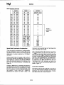
AD110/ADA110
User'sManual
ffi
RealTimeDevices,
Inc.
"AccessingtheAnalog World'ISO9001 and AS9100 Certified
ADllO/ADAllO
User'sManual
ffi
REALTIMEDEVICES,
INC.
Drive
820 NorthUniversity
PostOfficeBox906
StateCollege,
Pennsylvania
16804
Phone:(814)234-8087
FAX:(814)234-5218
Publishedby
RealTimeDevices,Inc.
820N. UniversityDr.
P.O.Box 906
StateCollege,PA 16804
Copyright@ 1991by RealTime Devices,Inc.
All rightsreserved
Prinredin U.S.A.
Rev.B 9211
TABLE OF CONTENTS
INTRODUCTION
(ADA1I0 Only)...........
Digital-to-Analog
Conversion
.......t-3
WhatComes
CHAPTER I - BOARD SETTINGS
Factory-Configured
SwitchandJumperSettings
P2- BaseAddress(FactorySetting:200hex(512decimal)).................
P3 - IntemrptChannelSelection(FactorySetting:Disabled)
P5- D/A OutputVoltageRange(FactorySetting:0 o +2.56vols) ...........
P6 - Single-EndedlDifferential
AnalogInput Select(FactorySetting:Single-Ended)
P7- ExternalTriggerIn (FactorySening:Disabled)
Sl - A/D Conversion
Rate(FactorySetting:7.5H2)
ChangingtheProgrammable
GainSenings........
CHAPTER 2 _ BOARD INSTALLATION
l-l
....................
...............1-3
..............1-4
..........1-4
.........1-5
..............1-5
.......................1-5
.......................1-6
................1-6
2-l
BoardInstallation.......
theAnalogInputPins
Connecting
Connectingthe Digital
Connecting
theTriggerIn andTriggerOutPins....
............2-4
........2-5
ConnectingttreReset
CHAPTER3 - HARDWAREDESCRIPTION
3-1
ProgrammablePeripheral
CHAPTER 4 _ BOARD OPERATION AND PROGRAMN{ING
Continuous
ConvertMode...........
D/A Convers
.............4.I
.........4-5
BA + 0: PPIPortA - ReadA/D Data(ReadOnly)
BA + l: PPIPortB - DigitalVO (ReadflMrite)
................
BA + 2: PPI Port C - A/D Conrol/DigrtalVO (Read/Write)
BA + 3: PPIConrolWord(ReadlTVrire).................
BA + 4: Status@eadOnly)...........
BA + 8: D/A Converter
(WriteOnly)...........
BASIC
Turbo Pascal
Turbo C
LexiconTestandDiagnostics
Too1.............
...................4-10
.........4-11
.....4-rl
....................4-t2
.....4-t3
..........4-13
.............4-14
CHAPTER 5 - CALIBRATION
..................
5-I
APPENDIX A - IlO SPECIFICATIONS
APPENDIX B - CONNECTORPIN ASSIGNMENTS..
APPENDIX C - COMPONENTDATA SHEETS
APPENDIX D _LEXICON 110...
APPENDIX E - WARRANTY....
Lt
.B-1
c-1
LIST OF ILLUSTRATIONS
1-1
t-2
1-3
r-4
l-5
l-6
t-7
1-8
2-l
aa
2-3
2-4
2-5
3-1
3-2
4-i
4-2
4-3
44
4-5
4-6
4-7
5-l
5-2
BoardLayoutShowingFactory{onfiguredSettings
BaseAddress
n ................
Jumper,
IntemrptChannelSelection
Jumper,P3 ...............
D/A OutputVoltageRange,P5 ...............
Single-Ended/Differential
AnalogInputSelect,P6................
ExternalTriggerIn, P7 ..........
AID Conversion
RateSwitch,S1................
ConrollingtheProgrammable
Gains
P4UO ConnectorPin
Assignments
Single-Ended
InputConnection..............
DifferentialInput ConnectionWithoutGroundReference
DifferentialInput ConnectionWith GroundReference....
Cascading
Two Boardsfor Simultaneous
Sampling
AD110/ADAII0BlockDiagram
D/A Converter
for ImprovedSenlingTime ............
Configuration
PPIInterconnect
Diagram
SeuingtheGainto 100UsingBit SetfiesetFunction......
SingleConvertModeTimingDiagram
ContinuousConvertModeTiming Diagram
SingleConvertModeFlow Diagram
Continuous
Convert,
ModeFlow Diagram
Boards,SingleConvertModeFlow Diagram
Cascaded
AdjustableVoltageSource..........
BoardLayoutShowingCalibration
Trimpots......
ul
................1-3
1-4
......................
.....................1-5
1-5
.............
........................1-5
..........1-5
..........1-6
...................1-6
...........-..........2-3
..............24
.......24
.........2-5
.................2-6
.........................3-3
................34
................4-3
.........4-4
................4-5
........4-5
....................4-6
............4-7
...........4-8
.....5-3
......................5-4
tv
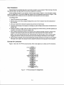
INTRODUCTION
i-2
The AD110 andADA110 differentialintegratinganalogI/O boardsturn your IBM PC/XT/AT or compatible
computerinto a high-performancedataacquisitionand control system.Installedwithin a singleshort or full-size
expansionslot in thecomput€r,each110seriesboardfeatures:
.
.
.
.
.
.
Onedifferentialor single-ended
analoginputchannel,
12-bitintegratingA/D converterfor high stabilityandexceptionalnoiseimmunity,
gainsof 1, 10,and 100,
Programmable
Trigger in and trigger out for cascadingboards,
12 TTL/CMOS digital I/O lines,
Single8-bit digital-to-analog
outputchannel(ADAI10 only).
The following paragraphsbriefly describettremajor functionsof the boards.More detaileddiscussionsof board
functionsareincludedin Chapter3, HardwareDescription,andChapter4,Board OperationandProgramming.T\e
boardsetupis de,scribed
in Chapterl,Board Settings.
Analog-to-DigitalConversion
The analog-to-digital(A7D)circuitry receivesa single-channeldifferential or single-endedanaloginput and
convertsthis input ino a 12-bit digital dataword which can thenbe readand,/ortransferredto PC memory.
The analoginput channelcanbe set for single-endedor differential operationby settinga jumper on the board.
Theinput voltagerangeis -5 to +5 volts for a gainof I (therangeis -0.5to +0.5volts for gain= l0; -.05to +.05
volts for gain = 166;.The conversionrateis switch-selectable
for eittrer7.5 or 30H2. The 7.5 Hzrate provideshigh
rejection(over60 dB) of 60 Hz line noise.
A/D conversions
areperformedby a 12-bit(plussignbit showingpolarity)dual-slopeintegratingconverter.
gainsof 1, 10,and 100let you discernchangesin theinput voltageas smallas 13microvolts.
Theprogrammable
The converteddatais readand/ortransferredto PC memory,onebyte at a time, throughthe PC databus.
Digital-to-AnalogConversion(ADA110Only)
The digital-o-analog(D/A) circuitryfeaturesa single8-bit D/A converterwhich hasa jumper-selectable
analog
oulputrangeof 0 to +2.56volts or 0 to +10 volts.D/A conversions
areriggeredby writing an 8-bit word to the
converter.Whenevera word is written to the D/A converter,it automaticallyperformsthe conversionand thenwaits
for moredata0obegin the next conversion.
Digital VO
The 110seriesboardshave 12 TTL/CMOS-compatibledigital VO lines which canbe directly interfacedwith
externaldevicesor signalsto senseswitch closures,rigger digilal events,or activatesolid-staterelays.The lines are
providedby tle on-board8255programmableperipheralinterface@PI) chip.
What ComesWith Your Board
You receivethefollowing itemsin your 110seriespackage:
. AD110 or ADAI 10interfaceboard
. Softwareand diagnosticsdiskefiewith exampleprogramsin BASIC, Turbo Pascal,and Turbo C; sourcecode
. IJser'smanual
pleasecall RealTime Devices'CustomerServiceDepartrnent
If any item is missingor damaged,
at
(814)234-8087.If you requireserviceoutsidetheU.S.,contactyour local distribuor.
In addition to the items includedin your ll0 package,Real Time Devicesoffen a full line of boardaccessories.
Key accessories
for the I l0 seriesincludethe ND(32analoginput expansionboardwittr 16differentialor singleendedinput channels,the TB40 terminalboardand XMO prototype/terminalboardfor prototypedevelopmentand
easysignalaccess,EX-XT andEX-AT extenderboardsfor simplified testingand debuggingof prototypecircuitry,
andTW40 twisted pair and XC40 singlewire flat ribbon cableassembliesfor extemalinterfacing.
i-3
UsingThis Manual
This manualis intendedto helpyou installyour newboardandget it runningquickly,while alsoproviding
enoughdetail aboutthe boardandis functionsso that you canenjoy maximumuseof its featuresevenin the most
We assumethatyou alreadyhavean understanding
complexapplications.
of dataacquisitionprinciplesandthatyou
cancustomizethe examplesoftwareor write your own apptcationsprograms.
When You NeedHelp
This manualand the exampleprogramsin fte softwarepackageincludedwith your boardprovide enough
informationto properly useall of theboard'sfeatures.If you haveany problemsinstalling or using this board,
contactour TechnicalSupportDepar0nent,(814) 234-8087,duringregularbusinesshours,qutern standardtime or
easterndaylighttime,or senda FAX requestingassistance
to (814)234-5218.Whensendinga FAX request,please
includeyour company'snameandaddress,your name,your telephonenumber,and a brief descriptionof the
problem.
i4
CHAPTER 1
BOARD SETTINGS
The 110boardhasjumperandswitchsettingsyou canchange
if necessary
for your application.Theboardis factory-configured
with the mostoftenusedsettings.The factorysettingsarelisted
and shownon a diagramin thebeginningof this chapter.Should
you needto changethesesettings,usetheseeasy-to-followinstructionsbeforeyou installthe boardin your computer.
Also notethatby installingresistorsat two locationson the
gain
board,R9 andR10,you canincreasetheprogrammable
settingsof x10 andx100to anyvaluesyou choose.The procedure
for customizingthe gainis describedat theendof this chapter.
1-t
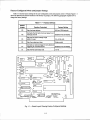
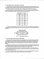
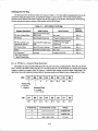
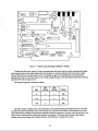
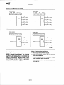
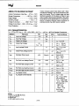
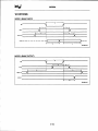
Factory-ConfiguredSwitchand Jumper Settings
Table l-1 liss tle factorysettingsof the user-configurable
switchandjumperson ttre110board.Figure1-l
showstheboardlayoutandthe locationsof thefactory-setjumpers.Thefollowingparagraphs
explainhow to
changethe factorysettings.
Table1-1- FactorySettings
Switch/
Jumper
FunctlonControlled
FactorySettlng
P2
Setsthe baseaddress
300 hex (768 decimal)
P3
Conneclsthe A/D End-of-convert
signalto an
interruptchannel
Disabled(not connectsd)
P5
Setsthe D/Aoulputvohagerange
(ADA110
only)
0 to +2.56vohs
P6
Setsthe analoginputtype
Single-ended
P7
Connects
an externallriggerfor simullaneous
of cascaded
boards
Disabled(notconnected)
triggering
S1
Setsthe A,/Dconversionrale
7.5Hz
=n
-U
,r'l
t255
_n
-l
I
"H
u2
sa
R..l Tim. O.vh.s, lm.
Sl.l. Coll.g., P.. 16E04
C23 Ur2
.- (-l
A D 1 1 o / A D A 1 1 o" _ l f i : : : : : l
& Control E?;#
DataAcquisition
pr A3r
System
H 7I ./ (f -f)/cfr e
f f
Ll
<3_9J
+ {_lclt
Settings
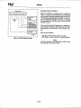
Fig.1-1- BoardLayoutShowingFactory-Configured
1-3
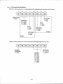
P2 - BaseAddress(Factory Setting:200 hex (512decimal))
Oneof themostcommoncausesof failurewhenyou arefirst trying your boardis addresscontention.Someof
your computer'sI/O spaceis alreadyoccupiedby internalI/O andotherperipherals.
Whenthe 110boardattempsto
useI/O addresslocationsalreadyusedby anotherdevice,contentionresultsandthe boarddoesnot work.
To avoidthisproblem,the 110hasa headerconnector,P2, whichletsyou selectany oneof eightstarting
in thecomputer'sI/O. Shouldthefactorysettingof 300hex (768decimal)be unsuitablefor your system,
addresses
you can selecta different baseaddress.Theseaddresses
are,from left o right on P2:
Hexadeclmal
Declmal
200
s12
240
576
280
640
2C0
704
300
768
340
832
380
896
3C0
960
To changethebaseaddresssetting,removethejumperfrom thefactorysetting(300hex)and,usingFigure1-2
asa guide,install it in thedesiredlocation.Recordthenewbaseaddresssettingon thetableinsidethe backcoverof
this manual.
ooPooo
ItoLtoto
orNN(9ctG,
P 2 8(\|
oooo
oooo
?o"
oooo
Fig.1-2- BaseAddress
P2
Jumper,
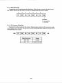
P3 - Interrupt ChannelSelection(Factory Setting:Disabled)
HeaderconnectorP3, locatednearthe bottom centerof the board,lets you connectthe A/D converter'send-ofconvertsignalto any of thecomputer'sintemrptchannels,IRQ2 (highestpriority channel)throughIRQT (lowest
priority channel).Thejumperis sored acrosstle top two leftmostpins,asshownin Figurel-3. By placingthis
jurnper vertically acrossthe pins of one of the IRQ channels,the end-of-convertsignalcan be usedto generate
intemrpts.
Before trying o useintemrpts,you mustbe familiar with theprocedurefor initializing the intemrpt vectorsand
the PC's interrupt controller,and seuingup the intemrpt handlingroutines.Theseproceduresare beyondthe scope
of this manual,but mustbe understoodo effectively useintemrptsin your computersystom.
Also, be careful to avoid contentionwith otherdevicesthat may useintemrpts in your computerwhen you
chooseyour intemrptchannel.To avoidcontention,usethetableinsidethebackcoverof this manualto recordthe
intemrptchannelyou haveselected.
It is alsovery importantto note that the boardinternrptsourceis a TTL totem-pole(pushlpull) type output; it is
Therefore,do not connectthis intenuptto anyotherintemrptoutput!
not open-collector.
t4
P3
a
E
HOOOO
oooooo
N(9rtn(oF
Fig. 1-3 -
InterruptChannelSelectionJumper, P3
P5 - D/A Output VoltageRange(Factory Setting:0 to +2.56volts)
P5, shownin Figure 14, setstheD/A outputrangeat0 n +2.56volts or 0 to +10 volts.Thisjumperis usedon
theADAIl0 boardonlv.
P5
nE=
Fig. 1-4 -
D/A OutputVoltageRange, P5
P6 - Single-Ended/DifferentialAnalog Input Select(Factory Setting:Single-Ended)
P6, shownin Figurel-5, setsthe analoginputchannelfor single-ended
or differentialoperation.
P6
tll
l.ol
SE
Fig. 1-5 -
DIFF
Single-Ended/DifferentiatAnalog
lnputSelect,P6
P7 - External Trigger In (Factory Setting: Disabled)
P7, shownin Figure 1-6,enablesanddisablesthe externaltrigger input. When thejumper is set to the enabled
position,the externaltrigger in pin (pin 10) at I/O connectorP4 is connectedto the A/D converterso that two or
moreboardscanbe run synchronouslyin a "master/slave"configuration.Note that this headerconnectorenables
and disablesthe nigger in only; it doesnot affect the trigger out
EXTTRIG
9z
out
Fig.1-6- ExternalTrigger
In,P7
l-5
Sl - A/D ConversionRate @actorySetting:7.5H2)
DIP switchSl., shownin Figure1-7,configurestheboardto performA/D conversions
at a rateof 7.5 converper second(30 Hz). Thefour switchesoperateasa goup. Whenatl of
sionsper second(7.5 Hz) or 30 conversions
the switchesarein the DOWN (closed)position,theconversionrateis 7.5 Hz. This settingprovidesmaximum
rejectionof 60 Hz line noise.When all of the switchesare in theUP (open)position, the conversionrate is 30 IIz.
When changingthe settings,makesureALL FOUR switchesareset to the sameposition.
Notethattheboardhasbeenfactory-calibrated
for a7.5Hz rate.If you changetherate,you may needto
recalibratethe board.Chapter5, Calibration, explainstheprocedures.
TT!T
30HZ
7.5H2
s1
Fig.1-7- A/DConversion
RateSwitch,
Sl
Changingthe ProgrammableGain Settings
gainsof l, 10,and 100.For evengrcatergainflexibility, two emptyresistor
The 110boardhasprogrammable
locationsareprovidedon yoru boardso that you canselectttregain valuesyou want. You canset ttrex10 gain input
to any valuegreater than xl0, andthex100gaininput to anyvaluegreater than 100.Notethat thegainscanonly
be increasedfrom their basevalues;they cannotbe decreased.
ResistorR9 controlsthe x10 input and shouldbe used
to covergainsfrom 10to 99.ResistorR10 controlsthexl00 input andshouldbe usedto setgainsof greaterthan
100.Figure 1-8 showshow theseresisbrs areconnectedto theFCA. The formulaswill help you find the correct
resistancevaluefor your desiredgain.Note that the further you get from the PGA's setgainsof 10 and 100,the
moregain drift you will have,which can causeerrorsin your readings.
R9= [10.8KfY(Desired
Gain- 10)]
R10= [108](Y(Desired
Gain- 100]
Values
Galn/Resistance
Galn
20
R9 Value
1.081(c)
R10Value
200
1.08KO
30
540cr
300
540fi
40
360rl
400
360c)
50
270r2
500
270A
Fig.1-8- Controlling
the Programmable
Gains
1-6
Gain
CHAPTER2
BOARD INSTALLATION
The 110boardis easyto installin your IBM PCIXT/AT or
compatiblecomputer.It canbeplacedin any slot,shortor fullsize.This chaptertells you step-by-step
how to install andconnect
the board.
2-l
2-2
Board Installation
Keepthe boardin its antistaticbag until you arereadyto install it in your computer.When removingit from the
bag,hold theboardat theedgesanddo not touchthecomponents
or connectors.
Beforeinstallingtheboardin your computer,checkthejumpersettings.Chapter1 reviewsthefactorysettings
andhow to changethem.If you needto changeanysettings,referto theappropriateinstructionsin Chapter1.Note
that incompatiblejumper settingscanresult in unpredictableboardoperationanderraticrcsponse.
To install theboard:
l. Turn OFF the power to your computer.
2. Removethe top coverof thecomputerhousing(referto yourowner'smanualif you do not alreadyknow
how to do this).
4. Selectany unusedshortor full-sizeexpansionslotandremovetheslot bracket.
5. Touchthemetalhousingof thecomputerto dischargeany stiaticbuildupandthenremovetheboardfrom its
antistaticbag.
6. Holdingtheboardby its edges,orientit so thatits cardedge(bus)connectorlinesup with theexpansionslot
connectorin thebottomof theselectedexpansionslot.
7. After carefullypositioningtheboardin theexpansionslot so thatthecardedgeconnectoris restingon the
computer'sbusconnector,gentlyandevenlypressdownon theboarduntil it is securedin theslot
NOTE: Do not force the boardino the slot. If theboarddoesnot slide ino place,removeit and try again.
Wiggling the boardor exertingtoo muchpressurecanresult in damageto the boardor to the comput€r.
8. After the boardis insalled, securethe slot bracketback ino placeandput the coverbackon your computer.
The boardis now readyto be connectedvia the externalVO connectorat the rear panelof your comput€r.
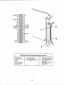
External VO Connections
Figure2-1 showsthe 110'sP4IIO connectorpinout.Referto this diagramasyou makeyour I/O connections.
NALOGGI'D
AOUT
l{,c.
L.c.
t{.c.
L.c.
IXALOG CI{D
N.C.
lt.c.
il.c.
A I N1 +
at,|t.
lt.c.
]t.c.
STATUS
DIOITALOI{D
TFIGOEROUT
DI6IIAL CND
TBIGGEBIN
DIGTTALC}ID
PC7
PC6
PC5
PCa
lt.c.
ltC.
1{.C.
BESET DRV
?47
PA6
PA5
PB'
PA3
Pa2
PBl
PBO
+12 VOLTS
.r2 volTs
+5 VOLTS
DIG]TALOiIO
Fig.2-1- P4l/OConnector
PinAssignments
2-3
Connectingthe Analog Input Pins
Single-Ended.Whenoperatingin the single-ended
mode,connectthehigh sideof theanaloginput to analog
input channelAINI+ andconnectthelow sideto AINI-, whichis a dedicatedanaloggroundin single-ended
operation.Figurc2-2 showshow theseconnections
aremade.
110
I/O CONNECTOR
P4
InputConnection
Fig.2-2 - Single-Ended
Differential. When operatingin the differential mode,twistedpair cableis recommendedo reducetlte effects
of magneticcoupling at the input. Your signalsourcemay or may not havea separategroundreference.Figure 2-3
showshow to connectthe input if you do not havea groundreferencefrom ttresignalsource,andFigure 24 shows
you how to makethe connectionswith a groundreferencefrom the signalsource.
If your signalsoarceDOESNOT HAVE a ground referencesignal:
. Refer to Figure 2-3 andinstall a 10 kilohm resistorbetweenAINI- (P4-I2) and ANALOG GND (P4-7)to
provide a referenceto ground.Next, connectthe high sideof the analoginput to analoginput channelAINI+
andconnectthelow sideof theinput to AINI-, asshownin Figure2-3.
110
I/O CONNECTOR
WithoutGroundReference
Fig.2-3- DifferentialInputConnection
24
It your signalsaurceHAS a groand referencesignal:
. Referto Figure24 andconnectthehigh sideof theanaloginput to analoginput,channelAINI+ andconnect
thelow sideof theinput to AINI-. Then,connectthegroundfrom the signalsourceto ANALOG GND
(P4-7',).
110
I/O CONNECTOR
SIGNAL
I
I+
souRcE
ou'
{
t'
GNO
Fig.2-4 -
DifferentialInput ConnectionWith Ground Relerence
Connectingthe Digital VO Pins
For all digital I/O connections,
PB0-7andPC4-7,thehigh sideof an extemalsignalsourceor destination
deviceis connectedo theappropriatesignalpin on theVO connector,andthelow sideis connectedto any DIGITAL GND.
Connectingthe Trigger In and Trigger Out Pins
The 110boardhasan extemalrigger input (P4-19)andoutput(P4-17)so thattwo or moreboardscanbe
cascadedandrun synchronouslyin a "master/slave"configuration.By cascadingtwo (or more)boardsas shownin
Figure 2-5, they canbe riggered to stafi an AID conversionat exactly the sametime.
Connectingthe StatusPin
The STATUS oueut canbe connectedto an externalcircuit which monitorsthe statusof the A,IDconverter.
Connectingthe ResetDrv Pin
The RESETDRV pin canbe usedto connecttheRESETsignalgeneratedby the PC o extemalcircuitry.
2-5
110
I/O CONNECTOR
P4
EOARDII
(HASTE R)
EXT TFIC
2a
l".il
R I G G E FO U T
l"' " I
P7
E O A N D1 2
( s L A vE )
3a
T N I G G E NI N
t"-,1
l" o'l
P7
Two Boardsfor Simultaneous
Sampling
Fig.2-5- Cascading
2-6
CHAPTER 3
HARDWARE DESCRIPTION
This chapterdescribesthefeaturesof the 110hardware.The
majorcircuitsarethe A/D, D/A, andtheprograrnmable
peripheral
interfacewhich includesthedigital VO lines.Boardintemrptsare
alsodescribedin this chapter.
3-2
peripheral
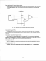
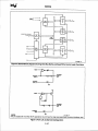
The 110boardhasthreemajorcircuis, theA/D, theD/A (ADAI l0 only),andtheprogrammable
interface@PI) which includesthe digital I/O lines.Figure 3-1 showsttreblock diagramof theboard.This chapter
describeshardwarewhich makesup themajorcircuits.It alsodiscusses
intemrpts.
0 TO +2.56v
0 TO +10.0V
Fig.3-1- AD110/ADA110
BlockDiagram
A/D ConversionCircuitry
conversions
on a singleanaloginputchannel.The following pamThe 110boardperformsanalog-to-digital
graphsdescribethe A/D circuitry.
Analog Input
The input type is jumper-selectablefor single-endedor differential operation.Single-endedoperationis
typically usedwhen the analoginput voltagesourceis closeto the boardand the volnge levelsarefairly high
(greaterthan10.5 vols for a gainof 1). Thedifferentialmodeprovidesnoiseimmunitywhenlong cablerunsare
signallevelsarelow, or surroundingelectricalnoiseis high.
unavoidable,
The input rangeis -5 o +5 volts for a gainof 1.Gainis usedto matchtheinput voltagelevelsbeingmeasured
ascloselyaspossiblewith theboard'sinput voltagerange.For analoginputsrangingbetween+500millivolts, a
gain of 10 can be used;and for analoginputsrangingbetween+50 millivolts, a gain of 100canbe used.In addition,
thex10 andx100gainscanbe increasedto any desiredvalueasdescribedat the endof Chapterl. Becauseit
theresolutionof theconversion.For example,
reducestheinput voltagerange,increasingthe gainalsoincreases
in thedigitizeddata.Althoughovervolt13
microvolts
reflected
are
whenthegain is setto 100,voltagechangesof
+12
whenusingthegains,not to
you
provided
especially
mustbe careful,
volts is
at theinput,
ageprotectionta
connectexcessiveinput voltagesto theboard.
J-J
A,/DConverter
The dual slopeintegratingAID converterperformsconversionsat a rateof either 7.5 or 30 times per second,
dependingon the settingof DIP switchSl. The outputis a l2-bit datawordplus a signbit which tells you whether
the digital valuerepresentsa positiveor a negativevoltage.
Theconvertersamplestheinput voltageovera windowof time beforeperformingtheconversion.Theconverter mq$ures the time requiredto chargeand dischargea capacitor.A counterand a referencein the A/D chip
determinethe integrationperiod. Becausethe input signalis sampledfor a specifiedperiod insteadof being instantaneouslycapturedby a sample-and-hold
device,spikesandglitcheswhich may be presentat theinput areaveraged
oul Theresultis a highly accurateconversion.
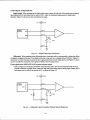
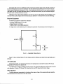
D/A Converter(ADA110Only)
A single8-bit digital-toanalogoutputchannelis includedon theADAll0 board.The outputvoltagerangeis
jumper-selectable
for 0 to +2.56voltsor 0 to +10 volm,providinga resolutionof 10.0or 39.1millivolts, respectively. When using the D/A converter,you may or may not noticethat the settlingtime for negative-goingoutput
voltagesmay be longer thanfor positive-goingoutputvoltages.This is becauseof the internalconsrucdon of the
D/A converterchip. If you want to improvethe negative-goingsettlingtime, you canadd a 24 kilohm pull-down
resistorbetweenthe D/A outputandthePC bus-12 volt supplyat externalI/O connectorP4, pin 20.Figwe3-2
canbe made.
showshow theseconnections
-12V
(P4-3s)
Time
Settling
Configuration
lor lmproved
Fig.3-2- D/AConverler
ProgrammablePeripheralInterface
The programmableperipheralinterface(PPI) is usedfor digital VO functions.This high-performarceTtLl
CMOS compatiblechip has24 digit:dI/O linesdividedinto two goups of 12lineseach:
GroupA - port A (8 lines) andport C upper(4 lines);
GroupB - port B (8 lines)andport C lower (4 lines).
Twelvelinesareusedfor on-boardfunctions.Port A's eightlinesareusedto readthe 8-bit MSB andLSB
outputsfrom the A/D converter.Port C's lower four lines areusedto control the gain selectionand the AID converter.The 12remaininglines in the groups,port B andport C upper,areavailablefor your use.Chapter4 explains
how you cancontroltheselines.
34
Interrupts
The 110boardprovidesan end-of-convertinterruptsignalwhich canbe used!o interruptthe computerwhenan
AID conversionis completed.This signalis the inverseof the stafts signalgeneratedby the A,/D converterand can
be connectedto any one of intemrpt lines IRQ2 throughIRQT by an on-boardjumper installedon headerconnector
P3. Theboardis shippedwith theintemrptsignaldisabled.If you connecttheend-of-convert
to oneof theintemrpt
channels,an intemrpt will occurwhenthe line transitionsfrom low (converting)to high (not converling).We
recommendthat you havean understandingof how to useintemrptsin your systembeforeyou connectthe end-ofconvertto an IRQ channel.
3-5
CHAPTER 4
BOARD OPERATIONAND PROGRAMMING
This chapterdescribesthe operatingmodesandprovidesflow
diagramsanda completedescriptionof the VO mapto aid you in
programmingyour 110board.The exampleprogramsincludedon
the disk in your boardpackagearelistedat theendof this chapter.
Theseprogftrms,writtenin BASIC, TurboPascal,andTurboC,
includesourcecodeto simplify your applicationsprogramming.
4-1
4-2
A/D Conversions
Beforeyou arereadyto starttaking A/D conversions,you must initialize theprogrammableperipheralinterface
(PPI) and selectthe gain (whenyou initialize the PPI, ttregain is automaticallysetto l). The softwareprovidedwith
your boardcontainsexampleprogramsfor boardinitialization.
You canmonitortheconversionstatususingthe statusbit at I/O addresslocationBA + 4. Whenbit 0 of this
word goeshigh, it meansa conversionis in progress.Whenit goeslow, theconversionis completed.Whenyou are
monitoringthe statusline, makesureyou seeit go high andthenlow beforeyou assumetle conversionis completed.This line doesnot go high until slightly after the StartConvertline startsa conversion,which meansthat you
could reada false low when ilte convenion first begins.(Rememberthat the statussignalis invertedto derive the
end-of-convertsignal which canbe monitoredthroughan IRQ line. The end-of-convertline is low during a conversionandgoeshigh whentheconversionis completed.)
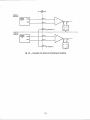
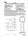
Initializing the PPI
Someof the lines of thePPI conrol the A/D convefierandset theprognmmablegain. The l2lines which are
usedduring A,/Dconversionare ttreeight lines of port A (PA0 throughPA7) andthe four lower lines of port C (pCQ
throughPC3).Port A's eight lines are usedto carry the converteddatr. This datais output from the A/D converterin
two 8-bit words, an MSB andan LSB. The four lines of port C lower areusedto control rhegain selectionand A/D
conversion.Figure4-1 showshow ttrePPI interfaceswiilr the converterandprogxammable
gain amplifier.
To settheselines up so that you cancontrol ttregain and takeA/D conversions,the PPI mustbe initialized
wheneveryou power up or resetyour system.This is doneby nwitingdatato thePPI control word at I/O address
location BA + 3. The I/O mapis definedlater in this chapter.The PPI mustbe setup like this:
D7
D6
D5
D3
D4
D2
D1
DO
X = userdefined(seeBA+ 3 registerdefinition
laterin thischapter)
EXT
TRIGGER
IN
A/D CONVERTER
82s5PPI
DO.D7
PORTA
(8 B|TS)
PORTB
(8 Btrs)
PCz
PORTC
PC4-7
(4 B|TS)
RN/HLD
HBEN
LBEN
STATUS
DIGITAL
lto
DIGITAL
vo
PC3
*/1
lr-
ecoI cArN
Pc1I sELEcr
STATUS
OUT
Fig.4-1- PPIInterconnect
Diagram
4-3
Settingthe Gain
You canset the gain by witing to lines PCOandPCI of port C, I/O addresslocation BA + 2. When you
initializethePPI,ttregainis automaticallysetto 1. Thegaincontrolsettingsare:
Galn
PCI
Setting
PC0
sening
x1
0
0
x10
1
0
x100
0
1
lnvalid
1
1
Note that when you write to port C to changettregain setting,you mustpreservethe other six bits of data(PC2
throughPC7)asyou hadttremif you wantthosesettingsto be unchanged.
Thereis a way to individually setandresetthe lines of port C by writing the correctdatato the control word at
addresslocationBA + 3. For example,you canindividuallyset(to logic 1) or reset(to logic 0) PCOandPCI by
writing two setsof datato the control word (not to pon C!) as shownin Figure4-2 below. This exampleshows
how to setthegainto 100.Whenthe mostsignificantbit" D7, of thecontrolword is setto 0, it activatesthebit
seVreset
functionwhich lets you individuallysetor resetany oneof port C's bits:
X
Sets PCOto 1:
(writtento BA+3)
D7
D6
D5
D4
D2
D3
D1
X = don'tcare
SeVReset
FunctionBit
DO
Set PCO
Bit Select
000= Pco
0
Sets PCI to 0:
(writtento BA+ 3)
D7
SeVReset
Functlon
lon Bit
D6
D5
D3
D4
D2
X = don'tcars
D1
DO
ResetPC1
Bit Select
001- PC1
Fig.4-2- Settingthe Gainto 100UsingBitSet/Reset
Function
44
A"/DConversionModes
The AID convertercanperform convenionsin two modes, SingleConvertatd Couinuous Canvert.The board
is typicallyusedin theContinuousConvertmode.
Two linesfrom PPI port C, PC2andPC3,areusedto conEoltheconversions.
Theselinescanbe setby writing
to PPI port C (BA + 2) or by usingthe singlebit set/resetfunction describedin the previoussection,Settingthe
Gain, andunderBA + 3 inthe Defining theIIO Map secton later in this chapter.PC2 conrols the StartConverr
function.WheneverPC2is high,conversions
canbe started.PC3determines
whichbyteof theconverteddata,the
MSB or theLSB, is to be readat PPIport A. WhenPC3is low, theMSB is read;whenit is high,theLSB is read.
For eachconvenion, the MSB is typically readfrst, followed by theLSB.
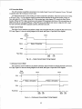
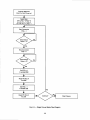
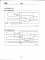
. SingleConvert Mode
The SingleConvertmodelets you performa singleA,/Dconversioneachtime you pulsethe StartConvertline,
PC2,high.Figure4-3 showsthe timing dia$am for thismode,andFigure4-5 providesa flow diagram.
Start
Convert
PC2
Done
I
-l
lr
Status
= Converting
Status
+
PC3
ReadData
MSB
LSB
Fig. 4-3 - SingleConvertMode Timing Diagram
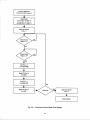
. ContinuousConvert Mode
The ContinuousConvertmodelets you performcontinuousA/D conversionsby keepingthe StartConvertline,
PC2, high. Figure4-4 showsthe timing diagramfor this mode,andFigure 4-6 providesa flow diagram.
Start
Convert
PC3
ReadData
MSB LSB
Fig.4-4- Continuous
ConvertModeTimingDiagram
4-5
MSB LSB
Program8255PPI:
PortA in, PortC-Lowout
SelectGain:
F o r x 1P
, C I = 0 , P C O= 0
F o r x 1 0P, C l = 1 ,P C O= 0
F o r x 1 0 0P, C I = 0 , P C O= 1
StartConversion
PC2=1
CheckStatus
Status= 1?
Stop Conversion
PC2=0
CheckStatus
Status= 0?
Set PCS-- 0
to enableMSB
ReadPPIPortA
for MSB
Set PCS= 1
to enableLSB
StopProgram
Fig.4-5- SingleConvertModeFlowDiagram
Program8255PPI:
PortA in, PortC-Lowout
SelectGain:
Forx1,PC1= 0, PCO= 0
F o r x 1 0P, C 1= 1 ,P C O= 0
Forx100,PCI = 0, PCO= t
StartConversion
PC2=1
CheckStatus
Status= 1?
CheckStatus
Status= 0?
Set PC3= 0
to enableMSB
ReadPPIPortA
lor MSB
Set PCS= 1
to enableLSB
ReadPPIPortA
lor LSB
StopConversion
PC2=0
StopProgram
Fig.4-6- Continuous
ConvertModeFlowDiagram
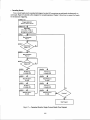
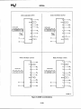
. CascadingBoards
Two or moreboardscan be cascadedand riggered so that A/D conversionsareperformedsimultaneouslyon
eachboard.Figure 4-7 providesa flow diagramfor cascadedoperation.Chapter2 showshow !o connectthe boards
for simulaneoustriggering.
BOARDS
I &2
Program8255PPI:
PortA in, PortC-Lowoul
BOARDS1 & 2
Selecl Caain:
Forx1,PC1=0,PCo=0
F o r x 1 0P,C 1= 1 ,P C o = 0
Forx100,PCI = 0, PCo= 1
Set PC3 - 0
lo enaHe MSB
Set PC3 = 0
to enaHe MSB
ReadPPI PortA
for MSB
Set PC3 = 1
to enaHe LSB
S€t PC3 = 1
lo enaue LSB
Fig.4-7- CascadedBoards,SingleConvertModeFlowDiagram
4-8
D/A Conversions(ADA110Only)
The single8-bit analogoutputchannelon theADAll0 boardletsyou generateoutputvoltagesin therangeof 0
to +2.56voltsor 0 to +10 volts,dependingon theP5jumpersetting.The0 to +2.56volt rangehasa bit weightof
10.0millivohs,andthe0 to +10 volt rangehasa bit weightof 39.06millivolts. OneVO write operationto address
locationBA + 8 loadsthe8-bit dataword into theD/A converterandstartstheconversion.
Digital VO
The programmableperipheralinrerfacehas24 digital I/O lines, 12 of which areavailablefor your use.The Z
linesaredividedinto three8-bit ports,port A (PA0-7),port B @80-7),andportC. Port C is furthersubdividedinto
port C lower (PC0-3)andport C upper(PC4-7).PortA andport C lower are alreadyusedby the boardfor AID
conversionand gain control. Port B andport C uppercanbe usedin this PPI operatingmodeonly:
Mode 0 - Basic inpuVouFut.Irs you usesimpleinput andoutputoperationsfor a port. Data is written to or
readfrom the specifiedport.
NOTE: If you know aboutthe operationof the 8255PPI or readthe includeddatasheet,thenyou may also
know that a two otler modes,mode I (srobed input/output)andmode2 (srobed bidirectionalinput/output),exist
for the chip. However,sincethesemodesrequirethe useof port C lower or port A, they are not availableon the ll0
board.
ThePPI is configuredby writing a controlword to its internalregisterat I/O addresslocationBA + 3. Six of the
eightbits in the conrol word arealreadydefinedby boardinitializationrequirements.
Theremainingtwo bits,bir 1
andbit 3, configureportsB andC upperasinput or outputports.SeethesectiononDefiningtheIIO Maplatern
this chapterfor a completedefinition of the PPI control word andports A, B, andC datawords. Seethe 8255PPI
datasheetin AppendixC for moreoperationalinformation.
Interrupts
The A/D converterstatussignalis invertedandsentto headerconnectorP3 asan end-of-convertsignalwhereit
canbejumperedto oneof six intemrptchannels,IRQ2 throughIRQ7.The end-of-convert
signalis low wheneveran
A/D conversionis in progess.Whenthesignalaansitionsto a high (logic 1) state,an intemrptis sentto the
computertelling it that the conversionis completed.Your boardis shippedwittr the interruptdisabled.
4-9
Definingthe VO Map
The VO mapfor the AD110andADA110 is shownin Table4-1.The baseaddress(designated
asBA) canbe
selectedby settingthejumperon P2,asdescribedin Chapterl, Board Seuings.Oneof eighrstartingaddress
locationscanbe selected.Theboardis shippedwith thebaseaddresssetat 300hex (768decimal).The following
sectionsdescribethe registercontentsof eachaddressusedin the I/O map.
Table4-1- ADl10/ADA110l/O
Map
ReglsterDescrlption
WriteFunctlon
ReadFunction
Address'
(Declmal)
PPIPortA (HeadData)
ReadA/Dconverteddata.
MSB& LSB
Notused
BA+0
PPIPortB
Read8 digitalinputlines
Program
8 digitaloutput
lines
B A +1
PPlPortC (PC0-3are
reserved
for control)
ReadPC4-PC7
digitalinput
lines
ProgramPC0-PCscontrol
lines& PC4-PC7
digital
outputlines
BA+2
PPlControlWord
Read PPI controlsettings
ProgramPPIconfiguration
BA+3
Status
ReadA/D converterstatus
Not used
BA+4
D/AConverter"
'BA = BgssAddress
'* ADA110boardonly
Notused
Program8-bitDAC
BA+8
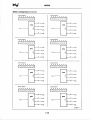
BA + 0: PPI Port A - ReadA/D Data (ReadOnly)
This addressis usedto readtheMSB andLSB of theA/D conversion,asdefinedbelow.WhenPC3of thePPI
port C word is 0, the MSB is read;whenPC3is l, theLSB is read.Bit 7 of theMSB tellsyou whethertheconverted
voltageis a positive or negativevalue.Bit 6 goesto 1 whenthe input voltageexceedsthe input voltagerange.The
tablebelow showsthe expectedconverteddatafor maximumpositiveand negativeinput voltagesand for 0 volts.
MSB
Bir11 Bir10
PolarityFlag
g = positive
1 = negative
LSB
Bir9
Bit8
OverrangeFlag
0 = in range
1 = out of range
D7
D6
D5
D4
D3
D2
D1
DO
Bh7
Bit6
Bir5
Bit4
Bir3
Bit2
Bir1
Bir0
PolarltyFlag
ConvertedData(12blts)
Voltage
0
1 1 1 1 1 1 1 11 1 1 1
volts
+4.99878
1
1 1 1 1 1 1 1 11 1 1 1
-4.99878volts
0
0000 0000 0000
0.0volts
4-10
BA + 1: PPI Port B - Digital VO (ReadAMrite)
Transfersthe 8-bit port B digital input anddigital outputdaa betweenthe boardandan externaldevice.A read
tnansfersdatafrom the externaldevicethroughP4 andino PPI port B; a write transfersthe witten datafrom port B
throughP4 to an extemaldevice.
ln7
In6
ln5
ln4
ln3
ln2
ln'l
ln0
D7
D6
D5
D4
D3
D2
D1
DO
OutT
Out6
Out5
Out4
OutS
Out2
Outl
Out0
BA + 2: PPI Port C - A/D Control/DigitatVO (Read/tVrite)
BA + 2 programsall eight PPI port C lines andreadsthe dataon t]report C upperlines. PCOt]rroughpC3 are
usedto programthe gain andto control the AID convert€r.PC4 throughPC7 ransfer digital input and digital outpur
databetweenthe boardand an extemaldevice.A readtransfersdatafrom the externaldevicethroughP4 andinto
PC4'7; a write transfersthe written datafrom PC4-7throughP4 to an ext€rnaldevice.
ln7
In6
In5
ln4
D7
D6
D5
D4
OutT
Out6
Out5
Out4
D3
D2
X
X
D1
DO
I
|
I
|
GainSelect
Sele
00=x1
o 1= x 1 o
1 o= x l o o
11= invalid
invali
|
Start Convert
0 - fiO @llVglt
1 = startc€nvert
ReadA/D Data
0 = readMSB
1 = rsadLSB
4-11
BA + 3: PPI Control Word (Read/Write)
Whenbit 7 of tltis word is setto 1, a write programsttrePPI configurationand a readshowsthePpI settings:
D7
D6
D5
D4
D3
D2
D1
DO
_l
t-
ModeSet F."'
i
1 = active
|
|
|
l"
rde SelEr;t
- mode I
= modg
t t = mode I
i3i
I
I
I
I
I
I'
I
|
I
Port A
0 s output
| = input
PortC
t C Lower
O =output
oul
1 = iinput
np
|
|
|
PortB
0 = output
1 = input
I
illode Selecl
0=mode0
1=mode1
Port C Upper
0 = output
1 = input
L_
__jyf_t
GroupA
Whenbit 7 of this word is setto 0, a write canbe usedto individually progam the port C lines:
D7
D6
D5
D4
D3
SeVReset
FunctionBlt
0 = activs
D2
Bft Select
000 = PCO
001= PC1
010=Pc2
011= PC3
100= Pc4
101= PC5
1 1 0= P C 6
1 1 1= P C 7
4-r2
D1
DO
Bit Set/Reset
Sel
0=S
sotbitto0
1=setbittol
BA + 4: Status(ReadOnly)
A readprovidesthe A/D converterstatusbit definedbelow. Whenyou starta conversion,the statusline goes
high.After the line goeshigh,thenwatchfor it to go low, signalingthattheconversionis complete.
A/D Status
0 = flotconverting
1 = converting
BA + 8: D/A Converter (Write Only)
Programsthe 8-bit dataword into tlre D/A converter.Wheneverdatais wriuen to the D/A converter,it simultaneouslytriggersan 8-bit conversion.The tablebelow showsthe correspondingoutputvoltagesfor all zeroesand all
onesdigital inpus to the converter.
MSB
D7
D6
D5
D4
D3
D2
D1
DigitalData(8 bits)
Voltage
0000 0000
0.0volts
1111 1111
+2.56or +10.0volts
4-13
DO
LSB
ExamplePrograms
The softwareincludedwith your 110boardcontainsexampleprogmmsin BASIC, Turbo Pascal,and Turbo C
to help you get startedusingthe board.Sourcecodeis alsoincluded.
The 110boardis easilyprogrammed
from any highJevellanguage'sVO referenceinstructions.In BASIC,
theseinstructionsareINP andOUT; in Turbo Pascal,they areport andport; and in Turbo C, they areinportb and
outportb.
Beforeusingthe sofrwareincludedwith your board,makea backupcopy of the disk. You may makeas many
backupsasyou need.The exampleprogramsincludedon the disk are listed below.
BASIC Programs:
GAINS.BAS
changingthe gain andperformingA/D conversions
performingA,/Dconvenions
READ.BAS
MVOLTS.BAS performingAID conversions
in millivolts
Turbo PascalPrograms:
ADC.PSL
INIT.PSL
PGA.PSL
MVOLTS.PAS
AUTO.PAS
DEMO.PAS
performinga singleA/D conversion
initiali2ingtheboard
settingthe gain
performingA7Dconversionsin millivolfs
autorangingthe DVM
a simpleA/D conversionprogram
Turbo C Programs:
PGA.H
INIT.H
ADC.H
READ.C
SIMPLE.C
MVOLTS.C
settingthe gain
initializingtheboard
performinga singleA/D conversion
performingA/D conversions
a simpleA/D conversionprogmm
performingA/D conversionsin millivolts
Lexicon Test and DiagnosticsTool
An interactivedacacollection andplotting utility program,Lexicon, is providediN a testand diagnosticstool.
This programis describedin Appendix D.
4-14
CHAPTER 5
CALIBRATION
This chaptertells you how to calibratethe 110usingthe four
trimpotson the board.Thesetrimpotscalibratethe A/D input
voltagerangeandgain.Calibrationmay berequiredif you change
the A/D conversionratefrom 7.5 to 30H2, or wheneveryou
suspectinaccuratereadings.
This chaptertells you how to calibratethe A/D convertergain andinput voltagerange.The D/A converteron
ADA1l0
the
boarddoesnot needto be calibrated.The offset and full-scaleperformanceof the board's A/D converter is factory-calibratedfor operationat7.sHz.If you changetle conversionrate,you may needto recalibrate
your board.Any time you suspectinaccuratereadings,you cancheckthe accuracyof your conversionsusingthe
procedurebelow, and makeadjustsasnecessary.
Calibrationis donewith the boardinstalledin your PC. You canaccessthe trimpos with the computer'scover
removed.Powerup the computerandlet the boardcircuitry stabilizefor 15 minutesbeforeyou startcalibrating.
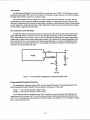
RequiredEquipment
The following equipmentis requiredfor calibration:
. PrecisionVoltage Source:0 to +5 volts
. Digital Voltmeter:5-12 digits
. Small Screwdriver(for trimpot adjustment)
A volage sourcecanbe madeusinga 9-volt batteryanda precisionl0-turn rimpot asshownin Figure5-1.
9 VOLTS
+
V = 0-6 volts
*
Fig. 5-1 - AdjustableVoltageSource
Figure 5-2 showsthe boardlayout. The four trimpotsusedfor calibrationareshadedin the upperright areaof
the board.
A/D Calibration
During this procedure,you will makeconnectionsto the analoginput at externalVO connectorP4. The pin
assignmentsfor P4 aregiven in AppendixB.
Two adjustrnentsare madeto calibratethe A/D converter.One is the offset adjustrnent,and the other is the fullscaleadjustment.Trimpots TR2 throughTR4 adjustthe offset, andTRl adjustthe full-scale voltage.
Offset Adjustment
for the inherentoffset outputvoltageof the programmablegain amplifier.
The offset adjustrnentcompensates
Threeadjusrnentsmustmade,onefor eachgain setting.
5-3
,&
flO*
cr
R'
O*
....{Tns
fg
r-F'L--rct
il'"il l'"
'ol
I
I
rn
cl6
C)
?a
a.2a
a {-F
llr
c -1--r
U
c27
utt s
E:t55
Trimpots
Fig.5-2- BoardLayoutShowing
Calibration
To adjustthe offset eror, connect0 vols o the analoginput (this canbe doneby simply connectingthe analog
mode).Setthe gain to 1, andstartcontinuousA/D conversions.Adjust
input to groundwhenin the single-ended
rimpot TR2 until the conversionoutputis zero.Then changethe gain o l0 andrepeatthe conversionp(rcess,
adjustingTR3 until the conversionoutput is zero. Finally, changethe gain to 100,and repeatthe procedure,this time
adjustingTR4 until the outputis zero.
The trimpot assignmentis summarizedbelow:
Galn
PC1
Settlng
PC0
Settlng
Trlmpot
x1
0
0
TR2
x10
1
0
TR3
x100
0
1
TR4
The offset voltage is relatedsolely to the performanceof the programmablegain amplifier; however,the offset
can affect the rollover performanceof the A/D converterif it is not set to zero.Rollover is the differencein conversion resultsbetweenvoltageshavingthe sameamplitudebut different polarities.Any gainswhich do not havea zero
offset will give readingsthat are shifted from an ideal zeroreference.This meansthat the positive and negative
readingsfor the samevoltage will be slightly different. This differenceis causedby the offset.
54
Full-ScaleAdjustment
The full-scale adjustmentcalibratesthe referencevoltageusedby the A/D converterto compensatefor the
analoginput circuitry.
Setthegainto 1, startcontinuousA/D conversions,
anddisplaytheconversionresults.Apply thevoltagesottrce
to theanaloginput andadjustit so thatit reads4.9982volts (4998.2millivolts) (seeTable5-1).AdjusttrimpotTRI
until the conversiondaa flickers betweenall ls and 0 in the leastsignificantbit place(hexadecimalFFF andFFE).
Changethegain to 10,andrepeattheprocedure,
this time usingan input voltageof .49982volts (499.82millivolts).
Finally, repeatthe procedure,changingthe gain to 100and sefiingthe input voltageat .044982volts (49.982
millivolts).
Table 5-1 providesa referencefor the ideal A/D converterinput voltagefor eachbit weight in eachvoltage
range.The first line is the ideal full-scale(all ones)value,andeachsuccessiveline decreases
by onebit weight.
Betweenthefull-scalevoltageandttrenextlowerbit weightis thevoltagevaluefor full-scaleminus 1-l/2 bits.Note
that the voltagevaluesin ttre tablearein millivolts.
Table5-1- A/D ConverterCallbratlonTable
ldeallnput Voltage(ln mlllivolts)
A/D Blt Welght
t5V(galn=1)
t0.5V (galn= 10)
1.05V(galn= 100)
4998.8
499.88
49.987
FS= 1-1t2LSB
4998.2
499.82
49.982
2048
2500.0
250.00
25.000
1024
1250.0
125.00
12.500
512
62s.00
62.500
6.2500
2s6
312.s0
31.2s0
3.12s0
't28
156.250
15.6250
1.5625
4095(FullScale)
64
78j25
7.812s
0.7813
32
39.063
3.9063
0.3906
16
19.s313
1.9s31
0.1953
8
9.7656
0.9766
o.0977
4
4.8828
0.4883
0.0488
2
2.414
0.24/1
o.o2u
1
1.2207
o.121
a.op2
5-5
APPENDIX A
I-10SPECIFICATIONS
ADf10/ADA110 Characteristics [email protected]
Interlace
IBMPC/XT/ATcompatible
Jumper-selectable
baseaddress,l/O mapped
Jumper-selectable
interrupts
Analog Input
1 single-ended
or differential
input
Inputimpedance..............
Gains,software-selectable
Gainerror
lnputrange..
protection
Overvohage
Commonmodeinputvohage
Settling
time.............
.........>10
megohms
..............1
,10, 100
....0.5%,
typ;1%,max
+0.5,or t0.0Svolts
................15,
..112Vdc
...110vohs,max
psec,max
....................5
A/DConverter
..............
tcLTlog
Type '...........
...............Dua1
slopeintegrating
with autozero
Resolution
.........12bitsplus sign
Conversionrate..............
.........7.5190
Hz, switch-selectable
Relativeaccuracy(gain= 1) .................
..11 bit
Linearity(gain= 1)..................
...................11
bit (7.5 Hz),13 blts (30 Hz)
Rollovererror.............
........t1bit
Digltarr/o .............
..................cMos
82c55(optionatNMos8255)
Number
of lines
...................12
inputor output
Miscellaneous
Outputs(PCbus-sourced)
Resetoutput
*12 volts
Digitalground
D/A Converter (ADA110only) .........
Singlechannel
Resolution
Voltagerange,jumper-selectable
Settlingtime,to 0.20"/"FSR
0-2.56volts
0-10volts
Relativeaccuracy......
Full-scale
accuracy
Zero error
.AD5S8
.....8bits
.0 to +2.56,0 to +10volts
psec,typ;1.5psec,max
......0.9
psec,typ;3.0psec,max
.........2.O
t1 bit,max
.t2 bits,max
1 bit, max
CurrentRequlrements
+5 vo1ts........
+12vohs......
-12 vohs
.....................14
mA
..7mA
........6
mA
Connector
40-pin,rightangle,shroudedheaderwithsjectortabs
Size
Shortslot- 3.875"Hx 5.25"W(99mmx 134rnm)
A-3
APPENDIX B
CONNECTORPIN ASSIGNMENTS
B-2
N.C.
AOUT
il.c.
N.C.
N.C.
ANALOGGilD
N.C.
N.C.
N.C.
ANALOGGND
A l N l+
AINl-
il.c.
N.C.
STATUS
DIGITALGND
TRIGGEROUT
DIGITALGND
TBIGGERIN
DIGITALGND
PC7
PC6
PC5
PC4
N.C.
N.C.
N.C.
RESETDRV
P87
PB6
PB5
P84
PB3
PB2
PBl
PBO
+12 VOLTS
-12 VOLTS
+5 VOLTS
DIGITALGND
AD110/ADA110P4 Connector/MatingConnector
Manufacturer
110P4 Connector
P4 Mating Connector
Fujitsu
3M
RobinsonNugent
MrL C-83503
FCN-70sQ040-AUM
FCN.7O7B04O-AU/B
3417-7U0
IDS-C4OPK-C-SR.TG
M83503f-09
B-3
B-4
APPENDIXC
COMPONENTDATASHEETS
c-r
c-2
Intel82C55AProgrammable
PeripheralInterface
DataSheetReprint
c-3
c4
intel'
82C554
INTERFACE
PERIPHERAL
CHMOSPROGRAMMABLE
I ControlWord Read-BackCapability
r DirectBit Set/ResetCapability
. 2.5mA DC DriveCapabilltyon all l/O
Port Outputs
r Availablein 40-PinDIPand 44-PinPLCC
I Availablein EXPRESS
- StandardTemperatureRange
- ExtendedTemperatureRange
I Compatiblewith all Inteland Most
Other Microprocessors
r High Speed,"Zero Wait State"
Operationwith 8 MHz8086/88and
8 0 1 8 6 /1 8 8
l/O Pins
. 24 Programmable
I Low PoweTCHMOS
r CompletelyTTL Compatible
CHMOSversionot the industrystandard8255A generalpurpose
The Intel 82C55Ais a high-performance,
lt provides
programmablel/O devicewhichis designedfor use with all lntel and most other microprocessors.
programmedin 2 groupsof 12 and usedin 3 majormodesof operation.
24 llO pins whichmay be individually
The 82C55Ais pin compatiblewith the NMOS8255Aand 8255A-5.
in sets ol 4 and 8 to be inputsor outputs.In
ln MODEO, each groupof '12llo pins may be programmed
to haveI linesof inputor output.3 of the remaining4 pinsare used
MODE 1, each groupmaybe programmed
bus configuration.
for handshakingand interruptcontrolsignals.MODE2 is a strobedbi-directional
provides
low powerconsumption
The 82C55Ais fabricatedon Intel'sadvancedCHMOSlll technologywhich
with performanceequalto or greaterthan the equivalentNMOSproduct.The 82C55Ais availablein 40-pin
DIP and 44-pinplasticleadedchip carrier(PLCC)packages.
r e3 i i 3 c i ! i i r r
I
R€SCI
a
m
9
DI
r0
?c7
tt
N
rc
t2
rc
FC6
t5
0a
rcs
la
D6
lca
FCo
t5
06
t5
D7
FCl
l7
PPSFE:FiFFF
231256-31
l.EcrtusrrE
* ritcSs^
Flgure 1.82C55ABlock Diagiam
?3l256-2
Flgure2.82C55APlnout
Disgfamsar€ for pin relerenceonly.Package
sizesare not to scale.
g-124
S.Ptctnbc? 10t7
OrdcrttumDri 231256-004
. Pln
Symbol
PAs-o
m
es
GND
At-o
Plnilumber
Dlp
PLCC
1-4
2-5
5
6
6
7
7
8
8-9
9-10
Type
uo
I
NameandFunctlon
PORTA, PINS0-3: Lowernibbleof an g-bitdata outputlatch/
butferand an 8-bit data input latch.
READCONTROT
: Thisinputis towduringCpUreadoperations.
CHIPSELECT:
A lowon thisinputenables
the82C55Ato
respondto RE andWF signats.
FD andWRareignored
otherwise.
SystemGround
ADDRESS:
Theseinputsignals,
inconjunction
ffi andWF[,
controltheselectionof oneof thethreeportsor thecontrol
wordregisters.
A1
A6
o
0
0
1
1
0
RD
0
0
0
1
1
0
0
1
1
1
x
X
X
X
PCt-t
1 0 - 1 3 1 1 , 1 3 - 1 5 t/o
WF cs
1
0
1
0
1
0
0
1
0
0
1
1
1
0
0
0
1
0
0
0
0
1
0
0
X
X
1
1
1
0
InputOperatlon(Read)
PortA-DataBus
PortB-DataBus
PortC-DataBus
- DataBus
ControlWord
OutputOperatlon(Wrlte)
DataBus- PortA
DataBus- PortB
DataBus- PortC
DataBus- Control
DlsableFunctlon
DataBus-3-State
DataBus-3-State
PORTC, PINS4-7: Uppernibbleof an 8-bitdataoutputlatch/
butferand an 8-bitdatainputbuffer(no tatchfor input).This port
can be dividedintotwo 4-bitportsunderthe modecontrol.Eact,
4-bit port containsa 4-bit latchand it can be used for the control
signaloutputsand statussignalinputsin conjunctionwith ports
A and B.
PCo-g
14-17
16-19
l/o
PBo-z
18-25
20-22,
24-28
vo
PORTC, PINS0-3: Lowernibbleof PortC.
PORTB, PINS0-7: An 8-bitdataoutputlatch/bufferand an gbit datainputbutfer.
Vcc
Dz-o
26
29
27-34
t/o
SYSTEMPOWER:* 5V PowerSupply.
DATA 8US: Bi-directional,
tri-statedatabus lines,connectedto
systemdata bus.
RESET
35
30-33,
35-38
39
WF
36
40
37-40
41 -44
PAz-q
NC
1,12,
29,34
RESET:
A highonthisinputclearsthecontrolregister
andatl
portsaresetto th6inputmode.
WBITECONTROL:Thisinputis low duringCPUwrite
operations.
t/o
PORTA, PINS4-7: Uppernibbleof an 8-bitdaraoutputtatch/
bufferandan8-bitdatainputlatch.
No Connect
3-125
intef
82C55A
82C55AFUNCTIONAL
DESCRIPTION
General
peripheralinterface
The 82C55Ais a programmable
device designedfor use in Intel microcomputer
systems. lts functionis that of a generalpurposel/O
componentto interfaceperipheralequipmentto the
microcomputersystembus. The functionalconfiguration of the 82C55Ais programmedby the system
softwareso that normallyno externallogicis necessary to interfaceperipheraldevicesor structures.
Data Bus Buffer
This 3-statebidirectionalS-bit
butferis usedto interface the 82C55A to the systemdata bus. Data is
transmittedor receivedby the bufferuponexecution
of input or output instructionsby the CPU.Control
words and status informationare also transferred
throughthe data bus butfer.
Read/Wrlte and Control Loglc
The function of this block is to manageall of the
internal and external transfersof both Data and
Control or Statuswords.lt acceptsinputsfrom the
CPU Addressand Controlbussesand in turn,issues
commandsto both of the ControlGroups.
Group A and Group B Controls
The functional configurationof each port is programmedby the systemssoftware.In essence,the
CPU "outputs" a controlword to the 82C55A.The
control word containsinformationsuch as "mode",
"bit set", "bit reset", etc., that initializesthe functional configurationof the 82C55A.
Eachof the Controlblocks(GroupA and GroupB)
accepts"commands"from the Read/WriteControl
Logic, receives "control words" from the internal
data busand issuesthe propercommandsto its associaled ports.
ControlGroupA - PortA and PortC upper(C7-C4)
ControlGroupB - PortB and PortC lower(C3-C0)
The control word registercan be both writtenand
read as shown in the addressdecodetable in the
pin descriptions.Figure6 shows the controlword
format for both Read and Write operations.When
the controlword is read,bit D7 will alwaysbe a logic
"1", as this impliescontrolwordmodeinformation.
Ports A, B, and C
The 82C55Acontainsthree8-bitports(A, B, and C).
All can be configuredin a wide varietyof functional
characteristicsby the systemsoftwarebut each has
its own specialfeaturesor "personality"to lurther
enhancethe powerand flexibilityof the 82C55A.
Port A. One 8-bit data outputlatch/bufferand one
8-bit input latch buffer. Both "pull-up" and "pulldown" bus hold devicesare presenton PortA.
Port B. One 8-bit data input/outputlatch/butfer.
Only "pull-up"bus hold devicesare presenton Port
B.
Port C. One 8-bit data outputlatch/butferand one
8-bit data input buffer (no latchfor input).This port
can be dividedinto two 4-bit ports underthe mode
control.Each4-bit port containsa 4-bit latch and it
can be usedfor the controlsignaloutputsand status
signalinputsin conjunctionwith portsA and B. Only
"pull-up"bus hold devicesare presenton PortC.
for
See Figure4 for the bus-holdcircuitconfiguration
Port A, B, and C.
3-126
82C55A
lr Drl€cflil^t
oAY^ l|ll
or or
-6
rA
\
rattt
2312fi-3
Flgure3.82C55ABlockDlagramShowlngDetaBusBufferandRead/WriteControlLoglcFunclone
EITER'{AL
FoFr B,c
Hil
NTERilAL
DATA
frn
'i{OTE:
231256-4
Portpinsloadedwithmorethan20 pF capacitance
maynothavetheirlogiclevelguarante€dfollowinga hardwarereset.
Flgure4. Port A, B, C, Bus-holdConfiguration
3-127
82C55A
82C55AOPERATIONAL
DESCRIPTION
co?ttRoL woFD
D?
Mode Selection
Da
Dr
ca
D!
D2
ot
Do
There are three basic modes of operationthat can
be selectedby the systemsoftware:
Mode 0 - Basicinput/output
Mode 1 - StrobedInput/output
Mode 2 - Bi-directional
Bus
/
c.orrs
\
foFT c GorfEnl
l.lilPW
0. OUTrut
Whenthe resetinputgoes "high" all portswillbe set
to the inputmodewith all 24 port linesheldat a logic
"one" levet by the internal bus hotd devices (see
Figure 4 Note). After the reset is removed the
82C55Acan remainin the inputmodewith no addithe need
required.This eliminates
tional initialization
for pullup or pulldowndevices in "all CMOS" designs. Duringthe execulionof the systemprogram,
any of the other modesmay be selectedby usinga
single output instruction. This allows a single
82C55A to service a variety of peripheraldevices
with a simnlesoftwaremaintenanceroutine.
ioFr t
| . lNtul
0. OUTrul
mDE sl|Cc?rotl
O. llOD€ 0
t . il(X)E i
/
cno(ra
\
,oRr c tttr€il
t.lt|?Ur
0. OutruT
The modes for Port A and Port B can be separately
defined,while Port C is dividedinto two portionsas
All of
requiredby the Port A and Port B definitions.
the output registers,includingthe statusflip-flops,
will be reset wheneverthe modeis changed.Modes
may be combinedso that their functionaldefinition
can be "tailored" to almost any llO structure.For
in Mode0 to
instance;GroupB can be programmed
monitorsimple switch closingsor displaycomputational results, Group A could be programmedin
Mode 1 to monitora keyboardor tape readeron an
basis.
interrupt-driven
XNTA
t . litirt
O.OUTrul
sDE 3tL€CTtOal
O. rOOE0
Ol . raOOEI
tX. Lol 2
rcOE StT f LAG
I . lCYlVl
231256-6
Figure6. llode DefinltlonFormat
The modedefinitionsand possiblemodecombinaat firstbutattera cursory
tionsmayseemconfusing
reviewof the completedeviceoperationa simple,
Thedesignof the
willsurface.
logicall/O approach
82C55Ahastakenintoaccountthingssuchas effivs PG
cientPCboardlayout,@ntrolsignaldefinition
layoutand completefunctionalflexibilityto support
devicewithno exlernallogic.
almostanyperipheral
Such designrepresentsthe maximumuse of th€
pins.
available
SlngleBlt Set/ResetFeature
Any of the eightbitsof PortC can be Set or Reset
This featurere'
usinga singleOUTputinstruction.
appti'
in Control-based
ducessottwarerequirements
cations.
andBus
Figure5. BasicModeDeflnitlone
lnterface
Port
WhenPortC is beingusedas status/controllor
A or B, thesebitscanbe setor resetby usingtheBit
Set/Resetoperationiustas if theyweredataoutput
ports.
3-128
inbf
82C55A
InterruptControlFunctlons
oofaTFol roio
q
o.
q
D.
tX
I
lr
DO'IT
CARC
q
Dt
Dr
%
I
IIT SET/iTSC'
t-tCt
O. i€SEI
gT 9ELTC?
When the 82C55Ais programmedto operatein
mode1 or mode2, controlsignalsare providedthat
canbe usedas interruptrequestinputsto the CPU.
Theinterruptrequestsignals,generatedfromportC,
can be inhibited
or enabledby settingor resetting
theassociated
INTEflip-flop,
usingthe bit set/reset
functionof portC.
161-tTtElEfdtl
#
+l0
l r l 0 l l l 0 lr I 0 lr l l o l
+l0lolllll0l0ltlll&l
-FIoldliliFlifilil
Thisfunctionallowsthe Programmer
to disallowor
allowa specific
l/O deviceto intem.rpt
theCPUwithoutaffecting
anyotherdevicein the interruptstructure.
u? s€t/nEtft rLAo
O. ACTIYI
iNTEflip-flopdefinition:
231256-7
(BIT-SETFINTE
is SET-lntemrptenable
(BlT-RESET)-INTE
is RESET-Interrupt
disabte
Flgure 7. Blt Set/Reset Format
Note:
All Mask flip-flopsare automatically
reset during
modeselection
anddeviceReset.
3-129
intet
82Cs5A
Mode0 BasicFunctionalDefinitions:
r Two 8-bit ports and two 4-bit ports.
Mode0 (BaslcInput/Output).
Thisfunctional
con.
r
Any port can be inputor eutput.
figurationprovidessimpleinputand outputoperationsfor eachof thethreeports.No "handshaking" r Oulputsare latched.
is required,datais simplywrittento or readfroma
. Inputsare not latched.
specifiedport.
o 16 difierentlnput/Outputconfigurations
are possiblein this Mode.
OperatlngModes
MODE0 (BASTC
TNPUT)
231256-S
MODEo (BASTC
OUTPUT)
3-130
intef
82Cs5A
MODE0 Port Deflnltlon
B
A
Da
D3
D1
Dq
0
0
0
0
0
0
0
0
1
1
1
1
0
0
0
1
0
I
1
0
0
0
0
0
0
0
1
1
0
0
1
1
0
0
0
0
0
0
0
0
1
1
1
1
I
1
1
1
1
0
1
1
1
1
1
1
1
1
1
'l
0
1
0
1
GROUPA
PORTC
PORTA
(UPPER)
OUTPUT
OUTPUT
OUTPUT
OUTPUT
OUTPUT
OUTPUT
OUTPUT
OUTPUT
OUTPUT
INPUT
OUTPUT
INPUT
OUTPUT
INPUT
OUTPUT
INPUT
INPUT
OUTPUT
INPUT
OUTPUT
INPUT
OUTPUT
INPUT
OUTPUT
INPUT
INPUT
INPUT
INPUT
GROUP
B
PORTC
PORTB
(LOWER}
OUTPUT
OUTPUT
OUTPUT
INPUT
INPUT
OUTPUT
#
0
1
2
3
INPUT
INPUT
OUTPUT
OUTPUT
OUTPUT
INPUT
INPUT
OUTPUT
OUTPUT
OUTPUT
OUTPUT
INPUT
INPUT
OUTPUT
OUTPUT
OUTPUT
OUTPUT
14
INPUT
OUTPUT
15
INPUT
INPUT
4
5
6
7
8
I
10
11
't2
INPUT
INPUT
INPUT
INPUT
13
MODE0 Configuratlons
colYriot rono a0
corriol
woFo a
QDtOrO.03OrDrOo
0t0
0
0
o
o
0
or-oo-.
coirtRoL rroFo al
cdrtnoL wofio t3
o,
o. o, o.
I
3-131
0
0
0
ol
or
0
0
o,
oo
INPUT
INPUT
INPUT
INPUT
INPUT
inbf
82C55A
MODE0 Conflgurations (Continued)
coil?ioL
toRo
..
o,
D6
D3
D.
Dt
Or
Or
Oo
I
0
0
0
I
0
0
o
@xliol
roRo
coilrRoLr{oRoi
D, Or D, O.
0
I
Dr
O,
D,
oiolo
0
Oo
0
PAr+An
,^/&
PC#.
PCTJC.
Er{o
rcfo
PBrrSo
Br48o
a6
o,
D.
05
o.
o'
o:
D,
Do
PAr'\
PArt\
ttcrtc.
tcirc.
D:{o
o,
ot
o!
D.
ot
02
Er{o
tsrtso
rl+q
?6rt|\
cot{ltor woRo ar0
D, Dr D, O.
ol
o
D!
Oz
D,
0l0lt
0
Do
lo
PAT4AD
?A/t\
PCTPC.
tcrfi.
tC!+Co
Erfio
P3r?80
P3r+6!
O7€o-
coNrRoLwoFDall
o,
o.
D9 D.
or
o,
I
Da D,
0
0
D.
Ot
0
02
Ol
Oo
I
,Ar.t\
tar+\
)cftc.
]4fi.
Er{c
fcrrco
?ry\
laiao
1
231256-1
3-132
82C55A
IIODE0 ConflguraUonr(Continued)
@{|.rnotsroaoar
oror%o.ororotoo
coillRoL rvoRorta
orDr%DrDrDlOrOo
rlol0lrlrl0l0l0
0
@tlnol
fi)to ttt
qq%orDrorDrDo
I
0
0
I
cli?tor
0
0
o
I
0
0
wonD ,lt
I
23125€-12
Operatlngilodet
MODEI (Strobed Input/Output).This functional
providesa meansfor transfeningl/O
configuration
datato or from a specifiedport in conjunction
with
strobes
or "handshaking"
signals.
ln model, PortA
and PortB use the lineson PortC to generateor
acceptthese"handshaking"
signals.
Mode1 BasicfunctionalDefinitions:
o TwoGroups(GroupA andGroupB).
o Eachgroupcontains
one8-bitdataportandone
4-bitcontrol/dataport.
r The 8-bitdataportcan be eitherinputor output
Bothinputsandoutputsare latched.
o The4-bitportis usedfor controlandstatusof the
8-bitdataport.
3-133
int€t
82C55A
Input Control Slgnal Deflnltion
SiE (Strole Input). A "low" on this input loads
data into the inputlatch.
oofalEol ||oio
Dr Or tL O. Dr D, Or Oo
! rirE I
Ll-.i
IBF (lnput Buffer FullF/F)
tsr.r
I . liltut
0. OUTTUT
A "high" on this outputindicatesthat the data has
been loaded into the inputlatch;in essence,an acknowledgement.IBF is set by ffi ingl being low
and is reset by the risingedge of the RD input.
INTR (lnterrupt Request)
x)ot r tfoRT ]
A "high" on this outputcan be usedto interruptthe
CPU when an input device is requestingservice.
INTR is set by the STB is a "one", IBF is a "on€"
and INTE is a "one". lt is resetby the fallingedgeof
FiD. tnis procedureallows an input device to request service from the CPU by simplystrobingits
data into the port.
INTE A
Controlledby bit set/reset of PCa.
INTE B
Controlledby bit sat/reset of PC2.
231256-13
Flgure8. iIODEI Input
231256-11
Flgure9. ilODE 1 (StrobcdInput)
3-134
intef
82C55A
OutputControlSlgnatDeftntilon
6ff 1OutputBuff* Fu[ F/fl. The6EF outpurwitf
go "low" to indicatethat the CpU haswrittendata
outto thespecifiedport.TheOeF plf willbe setby
the risingedgeof the WF inputand resetby Affi
Inputbeinglow.
ER (actnow_ledge
lnput).A .'tow"on this input
informsthe82C55AthatthedatafromportA or port
B hasbeenaccepted.In essence,
a response
from
the peripheral
deviceindicatingthat it hasreceived
the dataoutputby the CPU.
INTR(lnterruptRequect).A ,.high",on
thisoutput
can be usedto intemlptthe CpOwhenan output
devicehas accepteddata transmittedbv the CpU.
INTRis set wh€nFffi is a ,.on€",6EF-isa .,one"
andINTEis a "on6".lt is res€tbythefallingedgeof
rut
I |ronr lt
wF'.
INTEA
Controlledby bit set/resetof pC5.
INTE B
Controlledby bit set/reset of pC2.
231256-15
Flgure10.MODEl Output
2 3 1 2 5 6 -1 6
Flgure11.ITODE1 (StrobedOutput)
3-135
inbf
82C5sA
Combinations of MODE1
definedas inputor outputin Mode1 to supporta widevarietyof strobed
PortA andPortB cbnbe individually
l/O applications.
EFA
fl3e
Fr^
|lF^
ooilrFot lIoRD
COilTNOL fi)RD
4DrDcD.DrDrOrDo
tNtn^
r{ttr
uo
uo
o3-Fr
lrE
A-CXr
tSfa
tNTRr
|l{lRt
rQ.r
t . IilPUT
0. Ourrut
WF
|ontA-lslRoBEoour?utl
FORTT-GIROaEDlXtUTl
toRTA-tElioetorNPutl
rcar!-tsrRo!EDourru?l
231256-'17
of MODE1
Flgure12.Gomblnatlons
OperatingModes
OutputOPeratlons
MODE 2 (Strobed BidirectlonalBus l/O).This
providesa meansfor com'
functionalconfiguration
on a
or structure
witha peripheraldevice
municating
and receiving
single8-oitbus for bothtransmitting
signals
bus l/O). "Handshaking"
data (bidrrectional
in
proper
discipline
flow
bus
provided
maintain
to
are
a similarmannerto MODE1. Intenuptgeneration
functionsarealsoavailable.
and enable/disable
6EF lOutputBufler Fult).The 6BF outputwill9o
"lorv" to indicatethat the CPUhas writtendataout
to portA.
Definitions:
MODE2 BasicFunctional
. Usedin GroupA only.
o One8-bit,bi-directional
busport(PortA) anda $
(Port
C).
bit controlPort
o Bothinputsandoutputsare latched'
o The S-bitcontrolport (PortC) is usedfoi control
bus port
and statusfor the 8-bit,bi-directional
(PortA).
INTE 1 flhe INTE Flip'Flop Associated wlth
6BT). Controlledby bit set/resetol PC6.
BidirectionalBus l/O ControlSignalDefinltion
INTR(lnterruptRequest).A highon thisoutputcan
be usedto interruptthe CPUlor inputor outputoper'
ations.
Affi (lcfnowledge).A "low" on thisinputenables
the tri-stateoutputbutferof PortA to sendout the
the outpulbufterwill be in the high
data.Othenilise,
impedancestate.
InputOperations
SiF (StroUeInput).A "low" on this input loads
dataintothe inPutlatch.
IBF(lnputBufferFullF/F).A "high"on thisoutput
indicaiesthat data has been loadedinto the input
latch.
INTE2 (TheINTEFlip-FlopAssoclatedwith IBF).
Controlledby bit set/resetof PCa.
3-136
intef
82C55A
coi ?Rot rcRo
6tl^
tQo
1 . UIPU'
0. OUrruT
r i'itr I
_l-_'_.i
FOAI t
I . lt{?t T
O. OUrrut
ffi^
T--'l
518^
tlfa
GFOtt I ra@E
0. rrcOE0
t.tOOCr
231256-18
Figure 13.MODEControt Word
231256-19
Figure14.MOOE2
OAYATMI
c'lr roarcttA
dF
lia?i
aur
Srl
tBi
PERI'HERAI.
aus
llta
o laFn
?€ir''rEna! ro trc56a
o taFiol
arE6a toPln?ilEt
r
Figure 15.MODE2 (Bidtrectionat)
NOTE:
Anyseguence
rylgfgffi occursbeforeAex-,andffi occursbeforeffi is oermissibte.
(INTR: IBFo Fliffi. STEI.n-6 + OEF. MIS o ffifr o ffi;
3-137
intef
82C554
MODE2 AND MOOEO (OUTPUT}
MODE 2 ANO MODE O (INPUTI
lnTRa
tqr\
6fi^
rm^
lca
DrOt\D.OrDrOtOo
ooa{rRol roiD
fc.
m^
q
t!Fa
fcr
ttFl
Ero
t/o
r/o
t4ao
MODE2 AND MODET ITNPUTI
q
tc!
?lrt\
?Ar'?^!
fct
?q
ff^
EI^
07 or o! o. ot o: or oo
EOTIFOL ITORO
fg
dFe
rq
lG-(^
oror%D.DtD2DtDo
tc.
-i^
fc.
tI|^
tq
llF^
rq
t!f^
rgre!
iR
E-t^
F-!^
MOOE 2 AND MODE T IOUTPUT}
Fo
rq
lcr
ttl ?i!
i;TwIfilq
fr-r^
4Dr%D.DrDrOrDo
Er
coNrRoL uvono
q
t3.r.tq
PCq
66-r.
l,ca
trh
IrC2
ffi"
fct
t!Fr
LJ?f!
tcr
litir
731256-21
Figure16.MODEtZ Combinations
82C554
ModeDeflnltlonSummary
MODEO
iloDE 1
MODE2
IN
OUT
IN
OUT
PAo IN
PAr IN
PAz IN
IN
IN
IN
IN
IN
IN
IN
IN
OUT
OUT
OUT
OUT
e
OUT
OUT
OUT
<_.)
IN
IN
IN
IN
IN
IN
IN
IN
OUT
OUT
OUT
OUT
OUT
OUT
OUT
OUT
PAg
PAa
PAs
PA6
PAz
IN
IN
IN
IN
IN
OUT
OUT
OUT
OUT
OUT
OUT
OUT
OUT
PBo
PBr
PBz
PBs
PBI
PBs
PBe
PBz
IN
IN
IN
IN
IN
IN
IN
IN
OUT
OUT
OUT
OUT
OUT
OUT
OUT
OUT
PCo
PCr
PCz
PGs
PCa
PCs
PCe
PCt
IN
IN
IN
IN
IN
IN
IN
IN
OUT
OUT
OUT
OUT
OUT
OUT
OUT
OUT
GROUPA ONLY
<-)
e
ouT
<--)
MODEO
ORMODE1
ONLY
INTRe INTRs
lBFs 6EFs
SrB-s Affis
t/o
t/o
t/o
INTRa INTRa
INTRa
smA t/o
SfE'A
t/o
r/o Affia
t/o 6B-14
lBFa
Affig
lBFl
SpecialMode Comblnatlon Conslderatlons
Thereare severalcombinationsof mod€spossible.
For any combination,some or all of the PortG lines
are usedfor controlor status.The remainingbitsare
eitherinputsor outputsas definedby a "Set Mode"
command.
Duringa rsad of Port C, the state of all the Port C
placed
lines,excepr
[nes,
the AUK
ACK ano
exceptrne
t tr ilnes,
lines,wilt
will ()9
be ptaceo
and !STB
on the databus. ln placeof the Iffi and ffi fine
states,flagstatuswill appearon the databusin the
PCz,PCr',and PC6 bit positionsas illustratedby
Figure'18.
Througha "Write Port C" command,only the Port C
pinsprogrammedas outputsin a Mode0 groupcan
be written.No other pins can be atfectedby a "Write
PortC" command,nor can the intenuptenableflags
be accessed. To write to any Port C output programmed as an output in a Mode 1 group or to
o6FA
changean inlerruptenableflag, the "Set/Reset Port
C Bit" commandmustbe used.
With a "Set/ResetPortC Bit" command,any Port C
line programmed
as an output(includingINTR,iBF
and OBF)can be written,or an interruptenableflag
can be eitherset or reset.PortC lines programmed
as inputs,includingffi and ffi lines,aCsociated
with Port C are not atfectedby a "Set/Reset Port C
Bit" command.Writingto the coresponding Port G
bit positionsof the ACK and STB lines with the
"Set/Reset Port C Bit" command will atfect the
GroupA and GroupB interruptenableflags,as illustratedin Figure18.
Current Drlve Capablllty
Any outputon PortA, B or C can sink or scurce 2.5
mA. This featureallowsthe 82CQ5Ato directlydrive
Darlingtontype drivers and high-voltagedisplays
that requiresuch sink or sourcecurrent.
3-139
82C55A
ReadingPort C Status
D7 D5
ln Mode0, PortC transfersdatato or fromthe pe'
to
ripheraldevice.
Whenthe82C55Ais programmed
or acfunctionin Modes1 or 2, PortC generates
de'
signalswiththe peripheral
cepts"hand-shaking"
vice.Readingthe contentsof PortC allowsthe programmerto tesl or verifythe "status" of each peripheraldeviceand changethe programflow accordingly.
II{PUTCONFIGURATION
D1
D3
D2
Da
D5
GROUPB
GROUPA
D7
OUTPUTCONFIGURATIONS
D1
D2
D5 D5 D4 D3
Ds
GROUPB
GROUPA
Thereis no specialinstruction
to readthe statusinformationfrom PortC. A normalread operationof
PortC is executedto performthisfunction.
D6
Flgure17a.MODE1 StatusWordFormat
Dt
D5
D5
Da
D3
D2
D1
D6
GROUPB
GROUPA
(Detrned
ByMode0 or Mode1 Selection)
Flgure17b.MODE2 StatusWordFormat
Posltlon
AlternatePortC PlnSignal(llode)
lnterruptEnableFlag
Affie (OutpuiMode1)orSTBs(lnputMode1)
INTEB
PC2
PC4
STEa(lnputMode1 or Mode2)
INTEA2
PC6
EKr (OutputMode1 or Mode2
INTEA1
Flgure18.InterruptEnableFlagsIn ModesI and 2
3-140
82C55A
ABSOLUTEMAXIMUMRATINGS*
Ambient
Temperature
UnderBias.. . .0'C to + 70'C
StorageTemperature ..- 65'Cto+ 150'C
Supply
Voltage
. . .. - 0.5to * 8.0V
OperatingVoltage
.... + 4Vto + 7V
Voltage
onanylnput..
.GND-2Vto + 6.5V
Voltage
on anyOutput. .GND-O.SV
to V96 + 0.5V
PowerDissipation
. . .1 Watt
'Notice: Slressesabove thoselisted under "Absolutd MaximumRatings"maycausepermanentdamage to the device.Thisis a stressrating only and
functionaloperatianof the deviceat these or any
otherconditionsabovethoseindicatedin the operationalsectionsof thisspecificationis not implied.Erposure to absolutemaximumrating conditionsfor
extendedperiodsmayaffect devicereliability.
D.C.CHARACTERISTICS
= +5V t10o/o,
T4 = 0'Cto70oC,Vcc
GND= 0V(fR: -40'Cto +Ss"CforExtendedTemperture)
Symbol
Parameter
Mln
Unlts
Max
TestCondltlonc
0
.
5
Vrt
lnputLowVoltage
0.8
V
vrx
InputHighVoltage
2.0
vcc
V
Vol
OutputLowVoltage
V
0.4
l9g : 2.5 mA
vox
OutputHighVoltage
3.0
V
lox : -2.5 mA
V66 - 0.4
V
IOH: -100pA
It
lnputLeakageCurrent
t1
pA
V1p: V66 to 0V
loru
OutputFloatLeakageCurrent
lonn
Darlington
DriveCurrent
t2.5
t10
pA
(Note1)
V1p: V66 to 0V
(Note2)
(Note4)
mA
PortsA, B, C
R61:
Vs11:
500O
1.7V
'1.0V
Vggl :
Port A only
lpnt
Port Hold Low LeakageCurrent
+50
+300
pA
lpnn
PortHoldHighLeakageCurrent
-50
-300
pA
lpxlo
Port Hold Low OverdriveCunent
-350
p.A
V9g7: 0.8V
lpxxo
Port Hold HighOverdriveCurrent
+350
pA
Vggl:
lcc
lccse
V66 SupplyCunent
10
mA
(Note3)
V66SupplyCunent-Standby
10
pA
V66: 5.5V
Vrn: Vcc orGND
PortConditions
lll/P : Open/High
OlP : OpenOnly
WithDataBus :
High/Low
6 : High
Reset: Low
Purelnputs:
Low/High
V9g1 : 3.0V
PortsA, B,C
I{OTES:
1. PinsA1,Ao,CS,WF, FD-,Reser
2. Data Bus;PortsB, C.
3. Outputsopen.
4. Limitoulput currentlo 4.0 mA.
3-141
3.0V
int€f
82C55A
CAPACITANCE
Tg : 25'C, V6g :GND = 0V
Ctr't
InputGapacitance
10
Unlts
pF
Cyo
l/O Capacitance
20
pF
Parameter
Symbol
Max
Mln
TestCondltions
plns
Unmeasured
to GND
returned
fc : 1 MHz(s)
NOTE:
5. Samplednol 100olotested.
A.C. CHARACTERISTICS
TA : 0o to 70'C, VCC: +5V +10o/o,
GND : 0V
-40"C
:
TA
to *85'C for ExtendedTemperature
BUS PARAMETERS
READ CYCLE
Symbol
82C55A-2
Parameter
llln
tnn
tnn
AddressStableBeloreffi.1
AddressHoldTimeAfterRE t
tRn
ffi PulseWidth
tRo
tor
DataDelayfromffi I
FD ? to DataFloating
1o
tRv
RecoveryTimebetweenRD/WF
200
Unlts
llax
0
0
150
120
75
Tert
Condltlons
ns
ns
ns
ns
ns
ns
WRITECYCLE
Symbol
82CssA-2
Parameter
tln
Unlts
Itlax
tRw
AddressStableBeforeWHJ
0
ns
twe
AddressHoldTimeAtterWF T
20
20
ns
ns
tww
WFIPulseWidth
100
ns
tow
DataSetupTimeBeforeWFlf
100
two
DataHoldTimeAtterWHf
30
ns
ns
ns
30
3-142
Tegt
Gondltlone
PortsA & B
PortC
PortsA & B
PortC
inbf
82C554
OTHERTIiIII{GS
Symbol
82C554-2
Parameter
Mln
Max
Unlts
Condltlons
350
ns
tws
trn
WR: l toOutput
PeripheralDataBeforeRD
0
ns
tHn
Peripheral
DataAfterFD
0
ns
tex
ACK-PulseWidth
200
ns
tsr
STEPulseWidth
100
ns
tps
Per.DataBeforeSTBXign
20
ns
tpx
Per.DataAfterSTE'Hign
Fffi:0toOutput
Affi : 1 to OutputFloat
50
ns
tno
tro
Test
175
ns
250
ns
150
ns
tnoe
WF I: l to OB F : O
A e R : O t o O B F -1:
150
ns
tsrs
S T E:iO t o l B F : 1
150
ns
tnrs
tnr
ffi:ltolBF:0
150
ns
RD:Oto|NTR:0
200
ns
tgr
StEi:ltolNTR:1
150
ns
tnrt
twr
{Q(-=lto|NTR:1
150
ns
WR:OtoINTR:0
200
ns
see note 1
tnEs
ResetPulseWidth
ns
see note 2
twog
20
500
NOTE:
1.INTRT meyoccurasearlyasWFt.
2. Pulsewidthof initialResetpulseafterpow€ron mustbe at least50 pSec.Subsequent
Resetpulsesmaybe 500 ns
minimum.
3-143
WAVEFORMS
xroDE0 (BAsrc|NPUT)
2312fi-22
iloDE o (BASTC
OUTPUT)
?31256,-23
intel
WAVEFORMS(continued)
|NPUT)
MODEI (STROBED
sr
taF
ilTn
F-o
lt'tuTtROt?CNI'HTFAL
-
-
lroDE .| (STROBED
OUTPUT)
m
gt
liTl
ffi
ct tttrt
231256-25
inbf
82C55A
WAVEFORMS(continued)
MODE2 (BIDTRECTTONAL)
DAIA
z,31256-26
Note:
Any sequenceq!q!q m occursbelore Fffi IHO SfB occursbeloreFl-Dis permissibte.
(INTR : IBF o FiA-SR. SFB . FD + 6FF. ilfiAffi o flffi r ffi;
WRITETIMING
READTIMING
231256-28
2312fi-27
A.C.TESTINGINPUT,OUTPUTWAVEFORI'
A.C. TESTINGLOAD CIRCUIT
Iq.-ilot
231256-29
?31256-30
'Vgp ls S€t At VariousVoltagesDuringTestingTo Guarantes
Th€ Specification.Cs IncludesJig Capacitanc€.
A.C. Teting Inguls Are Div€n At 2.4V For A Logic 1 Ard 0.45V
For A Logic 0 TimingMeasurements
fu€ Mad€ At 2.0VFor A
Loglc1 And 0.8 Fof A Logic0.
3-146
APPENDIX D
LEXICON110
D-2
INTRODUCTION
Lexicon 110is an interactiveprogam tailoredspecificallyto makefull andeasyuseof your 110analoginput
board.It hasthe characteristicsof a highly specificdataacquisitionlanguageandsomepropertiesof an operating
system.It canbe usedto acquireanalogdatain real time andassigna time value for post-acquisitionanalysis.Data
canbe plottedor movedbetweenthe gnphicstemplatesanddisk files.The files areMS-DOScompatibleandcanbe
by tlte user'sprogamsto performhighly specificanalyses.
accessed
TheLexicon 110commandsetletsyou
chuactprae your experimentto determinethe bestacquisitionrate to use,how rapidly the daa changes,and how
muchdatais beinggenerated.
If you write your own softwarein BASIC, Pascal,or C, you can still useLexicon to selecta correctbase
addressand to veri$ correctoperationof ttreboard.
DESCRIPTION
A l"exicon is a specializedvocabularyfor a particularsubject.I-exicon 110 is an extensionof Forth-83,a
languagelong usedfor solving complexprocessconEolanddataacquisitionproblems.Time+ritical ponionsof
Lexicon,suchasI/O, graphics,andBIOS callsarewrittenin assemblylanguage.
Lexicon 110is interactive,fast
executing,andlets you fully conEolof the I l0's hardwareresources
so thatyou canbecomemorefamiliar with
your system.Small programstlat collect dataor displayreadingscanbe usedto isolateand diagnoseanyproblems
suchasbaseaddresscontentionor signaldrift.
In contrastto menu-drivensoftware,Lexiconis command-driven.
Like DOS,a commandtypedin response
to a
promptis input to theLexiconsystem,interpreted,
andthenexecuted.
Lexiconusestheprompt,,ok" to let you
know a commandhasbeenacceptedwithout error.For examplethe command:
lOO READINGS
will result in 100A/D readingsin bis being takenanddisplayedacrossrhescreen.
NOTE: Lexicon requiresttratall commandsbe enteredin capital leuerswith at leastone spacebetween
Lexicondoesnot recognizelower-caseletters.
commands.
The operand"100" comesbeforethe operator"READINGS". Like Forth, Lexicon usesReversePolish Notation
- also calledRPN or postfix notation.The main reasonfor usinga stack-orientedlanguageis executionspeedand
easeof passingargumentsbetweencommands.In an RPN language,commandsor progmmstake or leavenumbers
as argumentsfrom that sack.
NOTE: On the ll0 board:
Gain
-4095Blts
+4095Bits
't
-5 volts
+5 volls
10
-500 millivohs
+500 millivohs
100
-50 millivohs
+50 millivolts
It is importantto rememberthat a commandlike READINGS in the aboveexamplemusthavea 16-bit integer
argumentprecedingit. If you type in READINGS with no argument,an eror will result How do you know if a
commandtakesan argumenton the stack?You mustreadtheLexicon commandlisted in the documentation.
The Lexicon commandsetdescribedlater showseachcommandin the following format:
READINGS ( n -)
On the HELP screenany commandlistedwith a 'n' in front of it requiresan argumenlFor example:
n READINGS
The n beforethe commandmeansthat a (n)umbermustbe enteredasan argument.The valid rangeof numbers
for l,exiconis -32767 a +32761.
D-3
LEXICON AND DOS
The Lexicon softwareis wiuen to run underthe MS-DOSoperatingsystemversion2.0 or greater.To insure
the softwarewill work on PC clones,muchof it is written in assemblylanguageusing the BIOS and DOS software
intemrpts.Insteadof communicatingdirectly with the computerhardware,the BIOS ROM or DOS takescareof
manycommonfunctionslike drawinga pixel,readingtime,changingvideomodes,anddisk I/O.
CertainLexicon 110functions- suchastime delays- areimplementedusingBIOSIDOSintemrpts.For
example,to tell time,Lexiconperformsa BIOS call IAH to obtainthenumberof lSth-secondclock ticks since
midnight.This meansthatwhentakingreadings,theclosesttheycanbe discernedis 1/18of a secondapart.This is a
limitation imposedby DOS.The correcttime of day readby this intemrpt is dependenton the correcttime being
enteredwhen you boot your machine.
INSTALLING LEXICON 110
Beforerunning lrxicon, we recommendthat you $e*rtea separateLexicon disk. This is doneby copying the
following files containedin the LEXICON subdirecory on the programdisk onto a blank formatteddisk:
LEXllO.COM
SETTJP.LEX
BLOCKS.BKS
SINE.DAT
Irxicon 110is suppliedasa .COM file and mustincludeseveralotherfiles in order to operateproperly.One
file that mustbe includedis SETUP.LEX,a small file loadedafter Lexicon is booted.This file containsthe base
addressof the I10. SETUP.LEXcanbe configuredfor othervaluesby the softwareso it canbooton an unusedI/O
location.BLOCKS.BKSis theLexiconfile thatcontainstheboot instructionsusedby thesystemto setsomeinitial
characteristicsand also lists the HELP screen.
Daa fiIes createdby Irxicon arealwaysfollowed by theextension.DAT, and havea specialintemal coding to
insurethat only kxicon createdfiles canbe loadedby the system.SINE.DAT is an exampleof a datafile and is
includedon your disk. It wasgeneratedby usinga 110boardto digitize the ouput of a sine wave signalgenerator.
To run Lexicon enterthe name:LEXl10 from DOS.Lexicon will load, zerothe internaldatabuffers,load a
setupfile, take 15 test AID readings,in bits, and displaya IIELP screen.It would be very helpfut if you havea
voltagesourceor batteryconnectedto the input of the 110board.This will enableyou to seeif the displayedvalues
matchand frack ttreinput voltage.
LOADING THE SAMPLE DATA
To examinethe contentsof the disk, usethe commandDIR just asyou would from DOS. To load a Lexicon file
(with the extension.DAT), use:
FLOAD < name >
This commanddisplaysthe direcory of the activedisk drive andpromptsfor a file name.After you entera file
name,it will be loadedinto the databuffen. The commandto display the datain the daa buffer is:
PLOT
presstheESCkey.
To exitthePLOTprogram,
D4
CHANGING THE DEFAULT BASE ADDRESS
If you changethe baseaddresssettingof the 110by repositioningthejumper pin at connectorP2, you must
inform Lexicontlratyou madethis change.Thecommandto do thisis ADDR. Lexiconmustbe madeawareof this
changeor it will attemptto communicate
with the 110at a differentaddressandwon't work at all. Lexiconboos up
at baseaddress512(200 hex). To changethe defaultbaseaddressto, for example,576(240 hex) on boot-up,rype
thefollowing:
576 ADDR
NEW
"576" is the decimalvalueof hex 240 on jumper P2, the secondjumper settingfrom the lefl Next type "Y" in
responseto the question.To perform a new initialization sequence,type the following:
LSU
STTINIT
LSU will Load SetUpand SUIMT will performa setupinitialization of the I10. The following cableshowsrhe
correspondingdecimalAexadecimalequivalentsof the eight P2 baseaddresses:
Hexadecimal
Decimal
200
512
240
s76
280
640
2C0
704
300
768
340
832
380
896
3C0
960
USING LEXICON 110
Beforedescribingthe Lexicon 110commandsin detail,therearea few items concerningthe operationof
Irxicon that shouldbe repeated.All commandsmustbe ente.red
in uppercasewith at leastonespacebe[ween
commands.The RETURN key mustbe pressedto executethe command(s).Irxicon is capableof handlingonly
16-bitintegernumbersasarguments;thatis, numbersrangingbetween-32,767and,+32,767.Numbers
entered
outsidethis rangewill result in indeterminatevaluesbeingplaceon the sack.
REMEMBER:
1. Enter all commandsin upper-caseletters
2. All commandsmust be separatedby at leastonespace
On bootup,all numbersenteredandoutputfrom Lexicon arein decimal.I*xicon canalsoopemtein hexadecimal, octal, and binary numberingmodes.Internally, all numbersarestoredin binary, but when enteringor displaying them,you can choosea different numberbaseusing the DECIMAL, I{EX, OCTAL, and BINARY commands.
However,be awarethat Lexicon will expectyour daa input o be consistentwith the curent numberbase.For
example,if you are in decimalmode,the hex numbersA throughF will not be accepted.Lexicon can alsobe usedto
changenumbersbetweenbases.The IIEX commandcanbe usedto convert tle P2 connector'shex baseaddress
valueso their decimalequivalents.The following examplesassumethe currentnumberbaseinitially is decimal.
D-5
TRY THIS:
HEX 2C0 DECIMAL .
DISCUSSION: The hex modeis selectedandthehexvalue2C0 is entered,convertedto decimalandprinted
usingtheDECIMAL and . commands.
The next examplesillustratehow Lexicon canchangethe numberbaseof valueswhich areinput to andoutput
from the computer.
TRY THIS:
346 HEX . DECIMAL
DISCUS$ON: Thenumber346(in thecunentnumberbase)is placedon thestack,thenumberbaseis
changedto hex, and the operator. prints the op of the stack.The commandDECIMAL returnsyou tll the
decimalmode.
TRY THIS:
BINARY 1101111001DECIMAL
.
DISCUSSION: Thebinarynumberbaseis selectedandthebinarynumber"110111100f is enteredon the
stack.DECIMAL switchesyou back to decimalmodeand .prints the decimalequivalenton the screen.
TRY THIS:
DECIMAL 3147BINARY . DECIMAL
DISCUSSION: Thedecimalmodeis selectedandthevalue3147is entered.BINARY switchesrhenumber
baseand .prints the binary equivalenton the screen.DECIMAL changesthe modeback to base10.
What doesthe operator. do? As we saideadier,. prints the top numberon the stackin the currentnumberbase
followed by a spaceon the screen.
TRYTHIS:
316.
DISCUSSION:The number346is enteredon thestack.Regardless
of thenumbersalreadyon the stack,it will
go on top. Then it prins the numberon the screenin the numberbasecurrently selected.
Typing . with nothing on the stackresultsin an error message.This is not a fatal enor. Sometimesnumberscan
accumulatrs
on the stackwithout you realizing it. You canget rid of the excessstacknumbersusing the . command.
D-6
LEXICONCOMMANDSET
The Lexicon commandsaredivided into four classes:A/D Connol, OperatingSystem,File Conrol,/Ilelp
Screen,andHigh-Irvel Commands.
Lettersin parentheses
aretheshort-handversionsof the commandswhich can
be enteredin oneor two keystrokes.
permitdirectcontrolof the 110board:
A/D Control. The A/D Controlcommands
COMMAND
ADC
DIFF
?ADDR
READINGS
READ (R)
IOMAP
STATUS (ST)
ADDR
1x
10x
100x
INIT
STACK
(- )
(- )
(- )
( n-)
(- )
(- )
(- )
( n-)
(- )
(- )
(- )
(- )
DESCRIPTION
Prints a singleA/D result in bits
Prints the DIFFERENCE betweenreadings
Prints the present110baseaddress
Displaysn A/D readings
DisplaysA/D readingscontinuously
Displaysthe 110'sVO map
Displaysthe current systemstatus
Setsa new baseVO address
Setsgain to I
Setsgain to 10
Setsgain to 100
Initializesthe 110board
Operating System.The OperatingSystsmcommandsconsistof utilitiesto changetheglobalsystemparameten suchastime delayand numberbase:
COMMAND
BYE
MS
?DELAY
TIMER
TX
HR
?BASE
BINARY
DECIMAL
OCTAL
HEX
DIR
CLS
STACK
(- )
(- )
(- )
( n-)
(- )
(- )
(- )
(- )
(- )
(- )
(- )
((-
DESCRIPTION
Exits Lexiconto DOS
Delayaccordingto the valuein TIMER
Prints the presentsystemdelay
Selecta time delay of n (dimensionless)
Selectstext modeon CRT
Selectshigh resotutiongraphicsmode
Displaysthe current number base
Selectsnumber baseof 2
Selectsnumber baseof l0
Selectsnumber baseof 8
Selectsnumber baseof 16
Displaysdirectory of selecteddrive
Clearsthe text screen
D-7
FiIe ControVHelpScreen.TheFile Control/HelpScreencommandsareusedto saveandloadthe extended
memoryarrayof acquireddataand the SETUPanay. TheseDOS files can alsobe loadedby otherMS-DOS
progrirms.A utility progam (SEE)permis examinationon the screenof the extendedarray data:
COMMAND
STACK
DESCRIPTION
FLOAD (L)
FSAVE (S)
SEE
NEW
LSU
HELP (H)
(-)
(-)
Loads a Lexicon data file
Savesa Lexicon data file
Examinesdata array starting a # n
Write presentsetupto SETUP file
Loadsthe configuration setupfile
Displaysthe Lexiconhelp screen
(n- )
(-)
(-)
(-)
High-Level Commands.The High-LevelCommands
areusedto collectandplot datain differentformats:
COMMAND
STACK
DESCRIPTION
coLLECr (C)
RC
ZERO
(-)
(-
Data collectionprogram
Resumedata collection
Zeroesdata buffers
Strip chart simulator
Full-scaleplotting program
Plots data in buffers
Continuousmillivolt display
Selectsdrive A
Selectsdrive B
Selectsdrive C
CHART
FS
PLOT (P)
-)
( -)
( -)
( -)
( -)
Mvs (M)
A:
B:
C:
CONTROLLING THE 110BOARD
A usefulcommandis READ. This commandwill takeAID conversionson a singlechannelandwill continuouslydisplaythemin bits on thescreen.This commandalsohasa shorthandform of 'R'.
Enteringthe commandREAD will causeA,/Dconversionsto be displayedasbits. pressingany key will halt the
acquisition.Changethe input voltageto ttre110boardandwatchtheOisplayeO
bits valueschangeaccordingly.The
inputrangeof the 1l0 is -5 o +5 volts,so -5 will be 4095 and+5 will be +4096birs for a gainof 1.
To determinethe defaultbaseaddress,channel,or input gain, enterthe commandSTATUS (ST).
TRY THIS:
10 READINGS
DISCUSSION: 10READINGSdisplays10AID conversions
on rle screen.
TRYTHIS:
READ (R)
DISCUSSION:READ (unlikeREADINGS)continuouslyperformsA/D conversions
anddisplaysthemin bits
until any key is pressed.It usesthe presentgain valueanddoesnot changethem.Pleasenote that since
READ is oftenused,it hastre shorthandform of "R". Tlpe in "R'and thesamecommandis executed.
D-8
TRYTHIS:
MVS
DISCUS$ON: MVS, like the commandREAD, takescontinuousAID conversions
anddisplaysthemin
miltvolts. MVS works only for a gain of 1. Pressingany key hals the conversions.
TRY THIS:
DIFF
DISCUSSION:DIFF is a programlhat continuouslyprintsout thedifferencebetweentwo successive
readings.
If the analoginput signalis perfectly stable,all thereadingswill be zero.If the signalis noisy, hasbase
addresscontention,or is rapidlychanging,thennon-zerovalueswill appear.Thisis a gooddebuggingutility.
CHANGING THE DEFAULT VALUE
As we sated earlier, whenLexicon is loaded,a small file calledSETLTP.LEXis loadedand usedto initialize the
110'sbaseaddressand gain. This file canbe changedto initialize the boardto your own specificationswith the
commandNEW. NEW displaysthe currentVO addressandgain, andasksif you would like to makethesevalues
the setupdefaults.If you respondwith "Y", they arewritten to ttreSETUP.LEXhle on the disk.
TRYTHIS:
NEW
DISCUSSION: NEW akes the presentvaluesof ttreI/O baseaddressand gain and writes themto the file
SETUP.LEXwhich is loadedwhen the systemboots.
TRY THIS:
LSU SI.JIMT
DISCUS$ON: LSU loadsthe setupfile from the disk into the initialization array.SUINTTis the setupinitialization procedurewhich reconfiguresthe 110for your new setupvalues.
LEXICON 110DATA FILES
Lexicon 110savesdatain DOS files. It alsohastheability to createandlist thefiles on a disk. All Lexicon
createdfiles havethe extension.DAT andan internalcodettrratidentifiesthe file asonecreatedby Lexicon. Files
witttout the extension.DAT and without the intemal codewill not be loaded.This specialencodingconsistsof the
extension.DAT anda decimal19in the thfudbyteof thefile.
TRY THIS:
DIR {..DAT
DISCUS$ON: Like the DOS equivalenf DIR can ircceptargumentsfrom the DOS commandline. This
exampleinstrucg Lexicon to display all files with the extension.DAT.
TRY THIS:
FLOAD SINE.DAT
DISCUSSION: The commandFLOAD (File Ioad) will load a Lexicon file into an exlendedarray so the data
can be plotted and examined.
TRYTHIS:
FSAVE < name>
DISCUS$ON: The commandFSAVE (File Save)will savettredaa storedin the extendedarray into the
specifiedfile (appendedwith the extension.DAT). It will prompt you for a file namero use.The first
elementof the createdfile is the numberof datapoins it conlains,the secondis the number19 (to codefor a
valid Irxicon datafile). The next elementscontainthe systemgain and delay.The acquireddatafollows.
This commandis abbreviat€d
as"S".
D-9
Datais storedin the extendedanay in a specialformaf A/D resulVtimeMSW (Most Significant Word)/time
LSW (LeastSignificantWord). Every A/D conversionis taggedwith a 32-bit time value (from the internal MSDOS timer). A 64K datafrle will consistof about22,W daa points and22,000doubleprecisiontime values.The
32-bittime valuerepresents
the numberof 1/18secondMS-DOSticks sincemidnight.
TRY THIS:
100SEE
DISCUSSION:The SEEcommandletsyou examinea datapoint andits 32-bittime tag.Fifty datapointsare
displayedin this format:
Data Point. #/Time/Value (bits)
The argumentfor the commandis the startingvalueyou want to examine.In this example,you will begin
looking at datapoint 100.Note ttratthe ftst datapoint you can usewith the SEEcommandis an argumentof '2".
PressingPgUp/PgDnscrolls ttrereadings;ESC will terminatethis command.
TRYTHIS:
C: DIR
DISCUS$ON: C: will selectdrive C asthe selecteddrive.DIR will list thedisk directory.
LEXICON 110PLOTTING
Irxicon includesseveralhigh-levelplotting programs.Becausea limited numberof datapointscanbe plotted
acrossthe screen(approximately1140),the datapointsarebrokenup into frames.One framecanbe displayedon
the screenat onetime and it consistsof two graphicsboxes.The plotting progams PLOT andFS display oneframe
of data.The PgUp,PgDn,and Homekeys areusedto displaythe nextfureviousframe of ttreextendedmemoryanay
andreturn o the first frame.When usedwittr the GRAPHICS.COMutility suppliedwith advancedversionsof DOS,
high-qualitygraphicsoutputscanbe dumpedto a compatibleprinter.
TRYTHIS:
PLOT
DISCUS$ON: Any datastoredin the databuffersis scaledto fit into the npo graphicsboxes.This program
displaysone frameof daa (which is about 1140points).Pressthe PgUp/PgDnor Home key to seettrenex/
previousframe of datadisplayedasa point plot on the screen.This commandcanbe usedwithout first
FLOADing a file, but most likely you will seenothingon the display,or perhapssomerandomdataleft over
from anotherprogram.Pressingthe ESC key terminatesit The numbersalong the X-axis of eachdisplay are
the array indicesof the daa points.This commandis abbreviatedas"P".
TRY THIS:
FS
DISCUS$ON: FS is a Full-Screendataplottingprogram.It displayshalf a frameof data.Ofren,darais more
easily understoodwhen a largerplot is displayed.This routine is also atractive whendaa is dumpedusing
theGRAPHICS.COMutility.
TRYTHIS:
CHART
DISCUS$ON: CHART imitatesa strip chartrecorderandwill graphicallydisplay the A/D readingsasa point
plot in real time. ESC terminatesttris program.
D-10
LEXICON 110UTILITY PROGRAMS
In Lexicon, all highJevel programssuchasCOLLECT, RC, CHART, andREAD can havea time delay
insertedto delaybetweeneachreading.To setthe time delay,usethe commandTIMER. For examplethe command
5000TIMER storesthe dimensionlessnumber5000in the variableDELAY. A delayof 5000correqpondsto a
delay of about 19 secondson a 4.77 MHz machine.It canbe scaledaccordinglyfor fast€rCPUs.To actuallyget a
feel for how long the delay is, usethe commandMS or READ.
TRY THIS:
500TIMER READ or 5000TIMER MS
DISCUS$ON: A value of 500 is enteredinto the time delayvariable.This is abouta 1.9 seconddelay between
readings.It is fasterfor higherclock speedsand will scalerp linearly.
OPERATINGSYSTEMCOMMANDS
The Lexicon OperatingSystemcommandsare usedto interfacewith the entire systemsuchasclearingthe
screenor changingthe numberbase.
cl,s (-)
Clearsthe text screen;works like the samecommandin BASIC.
rx (-)
Selectsthe video text mode.If your display appea$stuckin the high-resolutiongraphicsmode,enterTX to
return it to the text mode.
HR (_)
Selectsthe high-resolutionvideo mode.
?BASE(-
)
Prints ttrecurent numberbasein decimal.
BYE (-)
Exis Lexicon and returnsto DOS.
HIGH.LEVEL COMMANDS - DRIVE SELECTION
A: (-)
Selectsdrive A as the defaultdrive.
B: (-)
Selectsdrive B asthe default drive.
c: (-)
Selectsdrive C as tlre default drive.
D-l1
TRYTHIS: C: FSAVE
DISCUSSION:Selecsdrive C asthe defaultdrive for listing,loading,andsoring Lexiconfiles.
TRY THIS: A: DIR
DISCUSSION:This commandsequence
selectsdrive A asthedefaultdriveandlists thedirectory.
D.T2
APPENDIX E
WARRANTY
E-l
LIMITED WARRANTY
Real Time Devices,Inc. warrantsthe hardwareand softwareproductsit manufacturesandproducesto be free
from defectsin materialsand workmanshipfor one yearfollowing the dateof shipmentfrom REAL TIIvIE DEVICES. This warrantyis limited to the original purchaserof productand is not ransferable.
During the oneyearwarrantyperiod,REAL TIME DEVICES will repair or replace,at its option, any defective
productsor partsat no additionalcharge,providedttratthe productis returned,shippingprepaid,to REAL TIME
DEVICES. All replacedpars and productsbecomettrepropertyof REAL TIME DEVICES. nefo"e returning any
product for repair, customersare required to contactthe factory for an RMA number.
THIS LIMITED WARRANTY DOESNOT EXTEND TO ANY PRODUCTSWHICH HAVE BEEN DAMAGED AS A RESULT OF ACCIDENT, MISUSE, ABUSE (suchas:useof incorrectinput voltages,improperor
insufficient ventilation,failure o follow the operatinginstructionsthat are providedUynfAf- TIIvG DEVICES,
"ac8 of God" or othercontingenciesbeyondthe control of REAL TIME DEVICES), OR AS A RESULT OF
SERVICEOR MODIFICATION BY A}.IYONE OTI{ER THANREAL TIME DEVICES.EXCEPT AS EX.
PRESSLYSET FORTH ABOVE, NO OTIIER WARRANTIES ARE E)PRESSED OR IMPLIED, INCLUDING,
BUT NOT LIMITED TO, A}IY IMPLIED WARRANTIES OF MERCHANTABILITY AND FITNESSFOR A
PARTICULAR PURPOSE,AND REAL TIME DEVICESE)PRESSLY DISCLAIMS ALL WARRANTIES NOT
STATED HEREIN. ALL IMPLIED WARRANTIES,INCLUDING IMPLIED WARRANTIES FOR
MECHANTABILITY AND FTTNESSFOR A PARTICI.'LAR PURPOSE,ARE LIMITED TO T}M DURATION
OF THIS WARRANTY. IN T}IE EVENT TIIE PRODUCTIS NOT FREEFROM DEFECTSAS WARRANTED
ABOVE, TIIE PURCHASER'SSOLEREMEDY SHALL BE REPAIR OR REPLACEMENT AS PROVIDED
ABOVE. UNDER NO CIRCUMSTANCESWILL REAL TIME DEVICES BE LIABLE TO TTIE PURCHASER
OR ANIY USERFOR ANY DAMAGES,INCLUDING AI.{Y INCIDENTAL OR CONSEQUENTIAL DAMAGES,E)PENSES,LOST PROFITS,LOST SAVINGS,OR OTHERDAMAGES ARISING OUT OF TI{E USE
OR INABILITY TO USE TIIE PRODUCT.
SOME STATESDO NOT ALLOW TIIE EXCLUSION OR LIMITATION OF INCIDENTAL OR CONSEQIJENTIAL DAMAGES FOR CONSUMERPRODUCTS,AND SOME STATESDO NOT ALLOW LIMITATIONS ON HOW LONG AN IMPLMD WARRANTY LASTS, SO TIIE ABOVE LIMITATIONS OR EXCLU.
SIONS MAY NOT APPLY TO YOU.
TI{IS WARRANTY GIVES YOU SPECIFICLEGAL RIGIITS, AND YOU MAY ALSO HAVE OTIIER
RIGITTSWHICH VARY FROM STATE TO STATE.
E-3
E4
INDEX
A
G
AID Conversion i-3
ConversionModes 4-5
ContinuousConvert 4-5
SingleConvert 4-5
MSB andLSB 4-10
AID Converter 34
ConversionRate 3- 4
Analog Input 3-3
InputRange 3-3
InputType 3-3
Gain 1-6, 3-3, 44. Seec/soProgrammable
Gain
Settingthe Gain 44
GainSettings 1-6
I
I/O Connections 2-3
Analog Input 24
Differential 24
Single+nded 24
Digital VO 2-5
ResetDrv 2-5
Status 2-5
Trigger In and Trigger Out 2-5
VO lvlap 4-10
Definitions 4-10
Initialization 4-3
Insallation 2-3
Intemrpts 3-5, 4-9, SeealsoEnd-of-Convert
B
BoardAccessories i-3
BoardBlock Diagram 3-3
BoardInitialization 4-3. Seea/soInitialization
BoardLayout 1-3
C
Calibration 5-3
Full-ScaleAdjustment5-5
OffsetAdjustment 5-3
CascadingBoards 2-5, 4-8
CustomerService i-3
L
Lexicon D-3
o
OvervoltageProtection 3-3
D
P
D/A Conversion i-3,4-9
D/A Converter 34, 4-13
ImprovedSettlingTime 34
OutputVoltageRange 34
Differential Input 2-4
GroundReference 2-5
No GroundReference 24
DigitalI/O i-3,3-4, 4-9
P4UOConnectorPinout
2-3,B-3
Programmable
Gain 1-6, 3-3
ProgrammablePeripheralInterface 34, 4-3,
4-9, C-3
Bit Set/Reset 44
PPI Conrol Word 4-t2
S
E
SimulaneousSampling
2-5.
SeealsoCascading
Boards
Single-Endedlnput
24
SpecificationsA-3
Status 4-I3
Line 4-3
Status
End-of-Convert 3-5, 4-3
ExampleProgmms 4-14
F
FactorySettings l-3
P2, BaseAddress 14
P3,IntemrptChannelSelection 14
P5, D/A OutputVoltrge Range 1-5
P6, Single-Ended/Diff
AnalogInput Selecr l-5
P7, ExternalTriggerIn l-5
51, A/D ConversionRate 1-6
T
TechnicalSupport i4
w
Warranty E-3
I-l
110SeriesBoardUser-Selected
Settings
Basel/OAddress:
(hex)
IRQ GhannetSetected:
IRQChannel#
(decimal)