1
Freescale Semiconductor, Inc.
Order Number: MPC7400EC/D
Rev. 1.1, 11/2000
Semiconductor Products Sector
Freescale Semiconductor, Inc...
™
O
IC
EM
R,
O
CT
U
ND
C
IN
.
S
E
L
CA
MPC7400 RISC Microprocessor
S
EE
R
Hardware Specifications
F
BY
The MPC7400 is an implementation
ED of the PowerPC™ family of reduced instruction set computing (RISC)
V
microprocessors. This document
describes pertinent electrical and physical characteristics of the MPC7400.
HI of the
C
For functional characteristics
processor, refer to the MPC7400 RISC Microprocessor User’s Manual.
AR
Advance Information
This document contains the following topics:
Topic
Page
Section 1.1, “Overview”
Section 1.2, “Features”
Section 1.3, “General Parameters”
Section 1.4, “Electrical and Thermal Characteristics”
Section 1.5, “Pin Assignments”
Section 1.6, “Pinout Listings”
Section 1.7, “Package Description”
Section 1.8, “System Design Information”
Section 1.9, “Document Revision History”
Section 1.10, “Ordering Information”
2
4
7
7
25
26
29
31
43
43
To locate updates for this document, refer to the website at http://www.motorola.com/sps. For the most
current part errata document, please contact your Motorola Sales Office.
This document contains information on a new product under development by Motorola.
Motorola reserves the right to change or discontinue this product without notice.
© Motorola, Inc., 2000. All rights reserved.
PRELIMINARY—SUBJECT TO CHANGE WITHOUT NOTICE
For More Information On This Product,
Go to: www.freescale.com
Freescale Semiconductor, Inc.
Overview
1.1 Overview
The MPC7400 is the first implementation of the fourth generation (G4) of PowerPC microprocessors from
Motorola. The MPC7400 implements the full PowerPC 32-bit architecture and is targeted at both portable
and computing systems applications. Some comments on the MPC7400 (with respect to MPC750):
•
•
•
Freescale Semiconductor, Inc...
•
•
•
•
The MPC7400 adds an implementation of the new AltiVec™ technology instruction set
The MPC7400 includes significant improvements in memory subsystem (MSS) bandwidth and
offers an optional, high-bandwidth MPX bus interface
The MPC7400 adds full hardware-based multiprocessing capability, including a 5-state cache
coherency protocol (4 MESI states plus a fifth state for shared intervention)
C.
N
The MPC7400 is implemented in a next generation process technology for core
, I frequency
R
improvement
TO
C
The MPC7400 floating-point unit has been improved to make latency
U equal for double-precision
D
and single-precision operations involving multiplication
N
O
The completion queue has been extended to 8 slots
IC
M
There are no other significant changes to scalar pipelines,
E decode/dispatch/completion mechanisms,
Smodel
or the branch unit. The MPC750’s 4-stage pipeline
is unchanged (fetch, decode/dispatch,
E
L
execute, complete/writeback)
A
C
Figure 1 shows a block diagram of the MPC7400.
ES
CH
R
A
2
ED
V
I
BY
E
FR
MPC7400 RISC Microprocessor Hardware Specifications
PRELIMINARY—SUBJECT
TO CHANGE
WITHOUT
NOTICE
For More Information
On This
Product,
Go to: www.freescale.com
Reorder Buffer
(8 Entry)
Ability to complete up
to two instructions per clock
6 Rename
Buffers
FPR File
DBAT
Array
MPC7400 RISC Microprocessor Hardware Specifications
PRELIMINARY—SUBJECT TO CHANGE WITHOUT NOTICE
For More Information On This Product,
Go to: www.freescale.com
L2 Castout
L2 Bus Interface Unit
L2 Data
L2 Miss
Transaction
19-Bit L2 Address Bus
64-/128-Bit L2 Data Bus
Instruction
Reload Table L1Operations
Queue
Tags
32-Kbyte
i Cache
128-Bit
(4 Instructions)
L2 Controller
L2CR
L2 Tags
FPSCR
FPSCR
+ x ÷
FloatingPoint Unit
Reservation
Station
32-Kbyte
Tags D Cache
Completed Stores
64-Bit 64-Bit
R,
O
CT
U
ND
C
IN
32-Bit 60x/MAX Address Bus
64-Bit 60x Data Bus/128-Bit MAX Data Bus
128-Entry
DTLB
SRs
(Original)
Load/Store Unit 6 Rename
Buffers
+
(EA Calculation)
32-Bit
Finished Stores
Bus Interface Unit
Data Reload Data Reload Instruction Load Fold
Reload Queue Queue
Table
Queue
32-Bit
System
Register Unit
IBAT
Array
Data MMU
128-Entry
ITLB
SRs
(Shadow)
Instruction MMU
Reservation
Station (2 Entry)
PA
EA
O
IC
EM
Completion Unit
128-Bit
32-Bit
+
Integer
Unit 2
GPR File
S
128-Bit
+ x ÷
Integer
Unit 1
Reservation
Station
LE
A
SC
VSCR
6 Rename
Buffers
Reservation
Station
EE
R
F
VSIU VCIU VFPU
Vector ALU
Vector
Permute
Unit
VR File
Reservation
Station
64-Bit (2 Instructions)
Dispatch Unit
CTR
BHT
(512 Entry)
BY
Reservation
Station
LR
ED
V
I
Reservation
Station
Instruction Queue
(6 Word)
BTIC
(64 Entry)
Branch Processing
Unit
CH
R
A
2 Instructions
Additional Features
• Time Base Counter/
Decrementer
• Clock Multiplier
• JTAG/COP Interface
• Power Management
Fetcher
Instruction Unit
Freescale Semiconductor, Inc...
Freescale Semiconductor, Inc.
Overview
.
Figure 1. MPC7400 Block Diagram
3
Freescale Semiconductor, Inc.
Features
1.2 Features
This section summarizes features of the MPC7400’s implementation of the PowerPC architecture. Major
features of the MPC7400 are as follows:
•
Freescale Semiconductor, Inc...
•
•
•
•
•
•
4
Branch processing unit
— Four instructions fetched per clock
— One branch processed per cycle (plus resolving 2 speculations)
— Up to 1 speculative stream in execution, 1 additional speculative stream in fetch
— 512-entry branch history table (BHT) for dynamic prediction
C.
— 64-entry, 4-way set associative Branch Target Instruction Cache (BTIC) forIN
eliminating branch
delay slots
R,
O
Dispatch unit
CT
U
— Full hardware detection of dependencies (resolved in the execution
units)
D
N
— Dispatch two instructions to eight independent units (system,
O branch, load/store, fixed-point
IC AltiVec ALU)
unit 1, fixed-point unit 2, floating-point, AltiVec permute,
M
— Serialization control (predispatch, postdispatch,
SEexecution serialization)
Decode
LE
A
— Register file access
SC
E
— Forwarding control
RE
F
— Partial instruction decodeY
B
Completion
D
VE buffer
— 8 entry completion
I
H
— InstructionCtracking and peak completion of two instructions per cycle
R
A of instructions in program order while supporting out-of-order instruction
— Completion
execution, completion serialization and all instruction flow changes
Fixed-point units (FXUs) that share 32 GPRs for integer operands
— Fixed-point unit 1 (FXU1)—multiply, divide, shift, rotate, arithmetic, logical
— Fixed-point unit 2 (FXU2)—shift, rotate, arithmetic, logical
— Single-cycle arithmetic, shifts, rotates, logical
— Multiply and divide support (multi-cycle)
— Early out multiply
Three-stage floating-point unit and a 32-entry FPR file
— Support for IEEE-754 standard single and double-precision floating-point arithmetic
— 3 cycle latency, 1 cycle throughput (single or double precision)
— Hardware support for divide
— Hardware support for denormalized numbers
— Time deterministic non-IEEE mode
System unit
— Executes CR logical instructions and miscellaneous system instructions
— Special register transfer instructions
MPC7400 RISC Microprocessor Hardware Specifications
PRELIMINARY—SUBJECT
TO CHANGE
WITHOUT
NOTICE
For More Information
On This
Product,
Go to: www.freescale.com
Freescale Semiconductor, Inc.
Features
•
Freescale Semiconductor, Inc...
•
•
•
AltiVec Unit
— Full 128-bit data paths
— Two dispatchable units: vector permute unit and vector ALU unit.
— Contains its own 32-entry 128-bit vector register file (VRF) with 6 renames
— The vector ALU unit is further sub-divided into the vector simple integer unit (VSIU), the
vector complex integer unit (VCIU), and the vector floating-point unit (VFPU).
— Fully pipelined
Load/store unit
— One cycle load or store cache access (byte, half word, word, double-word) C.
IN
— 2 cycle load latency with 1 cycle throughput
,
— Effective address generation
OR
T
— Hits under misses (multiple outstanding misses)
UC
D
— Single-cycle unaligned access within double word boundary
N
O
— Alignment, zero padding, sign extend for integer register
IC file
M
— Floating-point internal format conversion (alignment,
normalization)
SE
E
— Sequencing for load/store multiples and string
operations
AL
— Store gathering
C
ES
— Executes the cache and TLB instructions
E
FR
— Big- and little-endian byte addressing
supported
BY
— Misaligned little-endian
supported
ED and AltiVec load/store traffic
— Supports FXU, V
FPU,
HI for all 4 architecture AltiVec DST streams
— Complete support
C
Level 1 (L1)
ARcache structure
— 32K, 32-byte line, 8-way set associative instruction cache (iL1)
— 32K, 32-byte line, 8-way set associative data cache (dL1)
— Single-cycle cache access
— Pseudo least-recently-used (LRU) replacement
— Data cache supports AltiVec LRU and transient instructions algorithm
— Copy-back or write-through data cache (on a page per page basis)
— Supports all PowerPC memory coherency modes
— Non-blocking instruction and data cache
— Separate copy of data cache tags for efficient snooping
— No snooping of instruction cache except for ICBI instruction
Level 2 (L2) cache interface
— Internal L2 cache controller and tags; external data SRAMs
— 512K, 1M, and 2Mbyte 2-way set associative L2 cache support
— Copyback or write-through data cache (on a page basis, or for all L2)
— 32 byte (512K), 64 byte (1M), or 128 byte (2M) sectored line size
— Supports pipelined (register-register) synchronous burst SRAMs and pipelined (registerregister) late-write synchronous burst SRAMs
— Core-to-L2 frequency divisors of ÷1, ÷1.5, ÷2, ÷2.5, ÷3, ÷3.5, and ÷4 supported
— 64 bit data bus
— Selectable interface voltages of 1.8, 2.5, and 3.3V.
MPC7400 RISC Microprocessor Hardware Specifications
PRELIMINARY—SUBJECT TO CHANGE WITHOUT NOTICE
For More Information On This Product,
Go to: www.freescale.com
5
Freescale Semiconductor, Inc.
Features
•
Freescale Semiconductor, Inc...
•
•
•
•
•
6
Memory management unit
— 128 entry, 2-way set associative instruction TLB
— 128 entry, 2-way set associative data TLB
— Hardware reload for TLBs
— 4 instruction BATs and 4 data BATs
— Virtual memory support for up to 4 exabytes (252) of virtual memory
— Real memory support for up to 4 gigabytes (232) of physical memory
— Snooped and invalidated for TLBI instructions
Efficient data flow
C.
N
— All data buses between VRF, load/store unit, dL1, iL1, L2, and the bus are
, I 128-bits wide
R
— dL1 is fully pipelined to provide 128 bits/cycle to/from the VRF O
CTL1s
— L2 is fully pipelined to provide 128 bits per L2 clock cycle to the
U
D and L2/bus
— Up to 8 outstanding, out-of-order, cache misses between N
dL1
O
— Up to 7 outstanding, out-of-order transactions on theIC
bus
M
— Load folding to fold new dL1 misses into older,Eoutstanding load and store misses to the same
S
line
E
L
— Store miss merging for multiple store misses
to the same line. Only coherency action taken (i.e.,
CtoA all 32
address only) for store misses merged
bytes of a cache line (no data tenure needed).
S
E
E
— 2-entry finished store queue and
4-entry completed store queue between load/store unit and dL1
FR
— Separate additional queues
for
efficient
buffering of outbound data (castouts, write throughs,
Y
etc.) from dL1 and D
L2 B
Bus interface
VE
I
H extension to 60X processor interface
— New MPXCbus
R
A
— Mode-compatible
with 60x processor interface
— 32-bit address bus
— 64 bit data bus
— Bus-to-core frequency multipliers of 2x, 2.5x, 3x, 3.5x, 4x, 4.5x, 5x, 5.5x, 6x, 6.5x, 7x, 7.5x,
8x supported
— Selectable interface voltages of 1.8 and 3.3V.
Power management
— Low-power design with thermal requirements very similar to MPC740 and MPC750.
— 1.8 volt processor core
— Selectable interface voltages below 3.3V can reduce power in output buffers
— Three static power saving modes: doze, nap, and sleep
— Dynamic power management
Testability
— LSSD scan design
— IEEE 1149.1 JTAG interface
— Array built-in self test (ABIST)—factory test only.
— Redundancy on L1 data arrays and L2 tag arrays
Reliability and serviceability
— Parity checking on 60x and L2 cache buses
MPC7400 RISC Microprocessor Hardware Specifications
PRELIMINARY—SUBJECT
TO CHANGE
WITHOUT
NOTICE
For More Information
On This
Product,
Go to: www.freescale.com
Freescale Semiconductor, Inc.
General Parameters
1.3 General Parameters
Freescale Semiconductor, Inc...
The following list provides a summary of the general parameters of the MPC7400:
Technology
0.20 µm CMOS, six-layer metal
Die size
7.86 mm x 10.58 mm (83 mm2)
Transistor count
10.5 million
Logic design
Fully-static
Packages
Surface mount 360 ceramic ball grid array (CBGA)
Core power supply:
1.8V ± 100 mV dc (nominal; see Table 3 for recommended
operating
R
TO
conditions)
I/O power supply
1.8V ± 100 mV dc or
,
2.5V ± 100 mV dc or
O
IC
EM
C
IN
.
UC
D
N
S are configuration pin selectable)
3.3V ± 5% (input thresholds
LE
A
SC
1.4 Electrical and Thermal
EE Characteristics
R
F
This section provides the AC and DCY
electrical
specifications and thermal characteristics for the MPC7400.
B
D
VECharacteristics
1.4.1 DC Electrical
I
CH
The tables in this section
describe the MPC7400 DC electrical characteristics. Table 1 provides the absolute
R
maximum ratings. A
Table 1. Absolute Maximum Ratings1
Characteristic
Symbol
Maximum Value
Unit
Note
Core supply voltage
Vdd
–0.3 to 2.1
V
4
PLL supply voltage
AVdd
–0.3 to 2.1
V
4
L2 DLL supply voltage
L2AVdd
–0.3 to 2.1
V
4
Processor bus supply voltage
OVdd
–0.3 to 3.465
V
3
L2 bus supply voltage
L2OVdd
–0.3 to 3.465
V
3
Processor bus
Vin
–0.3 to OVdd + 0.3V
V
2,5
L2 Bus
Vin
–0.3 to L2OVdd + 0.3V
V
2,5
JTAG Signals
Vin
–0.3 to 3.6
V
Input voltage
Storage temperature range
Tstg
–55 to 150
°C
Notes:
1. Functional and tested operating conditions are given in Table 3. Absolute maximum ratings are stress ratings only, and
functional operation at the maximums is not guaranteed. Stresses beyond those listed may affect device reliability or cause
permanent damage to the device.
2. Caution: Vin must not exceed OVdd or L2OVdd by more than 0.3V at any time including during power-on reset.
3. Caution: L2OVdd/OVdd must not exceed Vdd/AVdd/L2AVdd by more than 2.0V at any time including during power-on
reset.
MPC7400 RISC Microprocessor Hardware Specifications
PRELIMINARY—SUBJECT TO CHANGE WITHOUT NOTICE
For More Information On This Product,
Go to: www.freescale.com
7
Freescale Semiconductor, Inc.
Electrical and Thermal Characteristics
4. Caution: Vdd/AVdd/L2AVdd must not exceed L2OVdd/OVdd by more than 0.4V at any time including during power-on
reset. In addition, operation at nominal Vdd/AVdd/L2AVdd greater than nominal L2OVdd or OVdd in the 1.8V input
threshold select mode can cause erratic operation and AC timing values worse than described in this specification.
5. Vin may overshoot/undershoot to a voltage and for a maximum duration as shown in Figure 2.
Figure 2 shows the undershoot and overshoot voltage on the MPC7400.
(L2)OVdd + 20%
(L2)OVdd + 5%
(L2)OVdd
Freescale Semiconductor, Inc...
VIH
VIL
Gnd
Gnd - .3V
Gnd - 0.7V
CH
R
A
ED
V
I
BY
EE
R
F
LE
A
SC
S
O
IC
EM
R,
O
CT
U
ND
C
IN
.
Not to exceed 10%
of tSYSCLK
Figure 2. Overshoot/Undershoot Voltage
The MPC7400 provides several I/O voltages to support both compatibility with existing systems and
migration to future systems. The MPC7400 “core” voltage must always be provided at nominal 1.8V (see
Table 3 for actual recommended core voltage). Voltage to the L2 I/Os and processor interface I/Os are
provided through separate sets of supply pins and may be provided at the voltages shown in Table 2. The
input voltage threshold for each bus is selected by sampling the state of the voltage select pins at the
negation of the signal HRESET. The output voltage will swing from GND to the maximum voltage applied
to the OVdd or L2OVdd power pins.
Table 2. Input Threshold Voltage Setting
BVSEL Signal
Processor Bus Input
Threshold is Relative to:
L2VSEL Signal
L2 Bus Input Threshold is
Relative to:
0
1.8V
0
1.8
1
HRESET
2.5V
HRESET
2.5
1,2
1
3.3V
1
3.3
1
Notes:
1. Caution: The input threshold selection must agree with the OVdd/L2OVdd voltages supplied.
2. To select the 2.5 volt threshold option, L2VSEL / BVSEL should be tied to HRESET so that the two signals
change state together.
8
Note
MPC7400 RISC Microprocessor Hardware Specifications
PRELIMINARY—SUBJECT
TO CHANGE
WITHOUT
NOTICE
For More Information
On This
Product,
Go to: www.freescale.com
Freescale Semiconductor, Inc.
Electrical and Thermal Characteristics
Table 3 provides the recommended operating conditions for the MPC7400.
Table 3. Recommended Operating Conditions
Characteristic
Unit
Note
Core supply voltage
Vdd
1.8v ± 100mv
V
1
PLL supply voltage
AVdd
1.8v ± 100mv
V
1
L2 DLL supply voltage
L2AVdd
1.8v ± 100mv
V
1
BVSEL = 0
OVdd
1.8v ± 100mv
BVSEL = HRESET
OVdd
BVSEL = 1
OVdd
L2VSEL = 0
L2OVdd
L2VSEL = HRESET
L2OVdd
L2VSEL = 1
L2OVdd
Processor bus supply
voltage
Freescale Semiconductor, Inc...
Recommended
Value
Symbol
L2 bus supply voltage
Input voltage
Processor bus
L2 Bus
JTAG Signals
Die-junction temperature
D
Note:
BY
LE
Vin A
SC
Vin
E
E
FR T
Vin
C.V
N
I
V
1
V
1
V
1
V
1
V
1
GND to OVdd
V
1
GND to L2OVdd
V
1
GND to OVdd
V
1
0 to 105
°C
2
R,
3.3v ± 165mv O
CT
1.8v ± 100mv
U
N±D100mv
2.5v
O
IC3.3v ± 165mv
M
E
2.5v ± 100mv
S
j
1
E tested operating conditions. Proper device operation outside of these
1. These are the recommended
Vand
I
conditions is not guaranteed.
H
C
2. The extended temperature
parts have die-junction temperature of -40 to 105 ˚C.
R
A
Table 4 provides the package thermal characteristics for the MPC7400.
Table 4. Package Thermal Characteristics
Characteristic
Symbol
Value
Rating
CBGA package thermal resistance, junction-to-case thermal resistance (typical)
θJC
0.03
°C/W
CBGA package thermal resistance, die junction-to-lead thermal resistance
(typical)
θJB
3.8
°C/W
Note: Refer to Section 1.8, “System Design Information,” for more details about thermal management.
The MPC7400 incorporates a thermal management assist unit (TAU) composed of a thermal sensor, digitalto-analog converter, comparator, control logic, and dedicated special-purpose registers (SPRs). See the
MPC7400 RISC Microprocessor User’s Manual for more information on the use of this feature.
Specifications for the thermal sensor portion of the TAU are found in Table 5.
Table 5. Thermal Sensor Specifications
At recommended operating conditions (See Table 3)
Characteristic
Min
Max
Unit
Notes
Temperature range
0
127
°C
1
Comparator settling time
20
—
µs
2
MPC7400 RISC Microprocessor Hardware Specifications
PRELIMINARY—SUBJECT TO CHANGE WITHOUT NOTICE
For More Information On This Product,
Go to: www.freescale.com
9
Freescale Semiconductor, Inc.
Electrical and Thermal Characteristics
Table 5. Thermal Sensor Specifications
At recommended operating conditions (See Table 3)
Freescale Semiconductor, Inc...
Characteristic
Min
Max
Unit
Notes
Resolution
4
—
°C
3
Accuracy
-12
+12
°C
Notes:
1. The temperature is the junction temperature of the die. The thermal assist unit’s raw output does not indicate an absolute
temperature, but it must be interpreted by software to derive the absolute junction temperature. For information
. about the
use and calibration of the TAU, see Motorola application note, “Programming the Thermal Assist Unit N
in C
the MPC750
Microprocessor,” (order #: AN1800/D).
,I
R
2. The comparator settling time value must be converted into the number of CPU clocks that needO
to be written into the
T
THRM3 SPR.
C
3. Guaranteed by design and characterization.
DU
N
O
IC
M
Table 6 provides the DC electrical characteristics for the MPC7400.
SE
E
Table 6. DC Electrical
AL Specifications
C
At recommended operating conditions (See Table 3)
ES
E
Nominal
FR
Characteristic
Bus
Symbol
Min
BYVoltage1
ED
V
Input high voltage (all inputs except
1.8
VIH
0.65 *
HI
SYSCLK)
(L2)OVdd
C
R
A
2.5
VIH
1.7
Max
Unit
Notes
(L2)OVdd + 0.3
V
2,3
(L2)OVdd + 0.3
V
2,3
2,3
3.3
VIH
2.0
(L2)OVdd + 0.3
V
1.8
VIL
-0.3
0.35 * OVdd
V
2.5
VIL
-0.3
0.2 * (L2)OVdd
V
3.3
VIL
-0.3
0.8
V
1.8
CVIH
1.5
OVdd + 0.3
V
2
3.3
CVIH
2.4
OVdd + 0.3
V
2
1.8
CVIL
-0.3
0.2
V
3.3
CVIL
-0.3
0.4
V
Input leakage current, Vin = L2OVdd/
OVdd
Iin
—
10
µA
2,3
Hi-Z (off-state) leakage current, Vin =
L2OVdd/OVdd
ITSI
—
10
µA
2,3,5
1.8
VOH
(L2)OVdd–0.45
—
V
2.5
VOH
1.7
—
V
3.3
VOH
2.4
—
V
Input low voltage (all inputs except
SYSCLK)
SYSCLK input high voltage
SYSCLK input low voltage
Output high voltage, IOH = -6 mA
10
MPC7400 RISC Microprocessor Hardware Specifications
PRELIMINARY—SUBJECT
TO CHANGE
WITHOUT
NOTICE
For More Information
On This
Product,
Go to: www.freescale.com
Freescale Semiconductor, Inc.
Electrical and Thermal Characteristics
Table 6. DC Electrical Specifications (Continued)
At recommended operating conditions (See Table 3)
Nominal
Bus
Voltage1
Characteristic
Output low voltage, IOL = 6 mA
Min
Max
Unit
1.8
VOL
—
0.45
V
2.5
VOL
—
0.4
V
3.3
VOL
—
0.4
V
Cin
—
7.5
Capacitance, Vin = 0 V, f = 1 MHz
Freescale Semiconductor, Inc...
Symbol
R,
.
CpF
N
I
Notes
3,4
Notes:
TO
1. Nominal voltages; See Table 3 for recommended operating conditions.
C
2. For processor bus signals, the reference is OVdd while L2OVdd is the reference for the
L2 bus signals.
DU
N
3. Excludes test signals (LSSD_MODE, L1_TSTCLK, L2_TSTCLK) and IEEE 1149.1
boundary
scan (JTAG) signals.
O
CH
R
A
ED
V
I
BY
EE
R
F
LE
A
SC
S
IC
M
E
MPC7400 RISC Microprocessor Hardware Specifications
PRELIMINARY—SUBJECT TO CHANGE WITHOUT NOTICE
For More Information On This Product,
Go to: www.freescale.com
11
Freescale Semiconductor, Inc.
Electrical and Thermal Characteristics
4. Capacitance is periodically sampled rather than 100% tested.
5. The leakage is measured for nominal OVdd and Vdd, or both OVdd and Vdd must vary in the same direction (for example,
both OVdd and Vdd vary by either +5% or -5%).
Table 7 provides the power consumption for the MPC7400.
Table 7. Power Consumption for MPC7400
Processor (CPU) Frequency
Unit
350 MHz
Full-On Mode
Freescale Semiconductor, Inc...
Typical
4.6
2.0
W
1, 2
1.75
2.0
W
1, 2
600
600
mW
1, 3
1.0
1.0
W
1, 2
Doze Mode
4.4
Maximum
Sleep Mode
Maximum
BY
F
LE
A
1.75SC
E
RE
Sleep Mode—PLL andD
DLL Disabled
Typical
HI
VE
RC
AMaximum
.
R,
O
T 1, 3
C
11.3
W U
1, 2, 4
D
N
O
IC
1, 2
EM W
S5.0
W
9.9
Nap Mode
C
IN
5.3
Maximum
Maximum
Notes
400 MHz
Notes:
1. These values apply for all valid processor bus and L2 bus ratios. The values do not include
I/O Supply Power (OVdd and L2OVdd) or PLL/DLL supply power (AVdd and
L2AVdd). OVdd and L2OVdd power is system dependent, but is typically <10% of Vdd
power. Worst case power consumption for AVdd = 15 mw and L2AVdd = 15 mW.
2. Maximum power is measured at Vdd = 1.9V while running an entirely cache-resident,
contrived sequence of instructions which keep the execution units, including AltiVec,
maximally busy.
3. Typical power is an average value measured at Vdd = AVdd = L2AVdd = 1.8V, OVdd =
L2OVdd = 3.3V in a system while running a codec application that is AltiVec intensive.
4. These values include the use of AltiVec. Without AltiVec operation, estimate a 25%
decrease.
1.4.2 AC Electrical Characteristics
This section provides the AC electrical characteristics for the MPC7400. After fabrication, functional parts
are sorted by maximum processor core frequency as shown in Section 1.4.2.1, “Clock AC Specifications,”
and tested for conformance to the AC specifications for that frequency. The processor core frequency is
determined by the bus (SYSCLK) frequency and the settings of the PLL_CFG[0–3] signals. Parts are sold
by maximum processor core frequency; see Section 1.10, “Ordering Information.”
12
MPC7400 RISC Microprocessor Hardware Specifications
PRELIMINARY—SUBJECT
TO CHANGE
WITHOUT
NOTICE
For More Information
On This
Product,
Go to: www.freescale.com
Freescale Semiconductor, Inc.
Electrical and Thermal Characteristics
1.4.2.1 Clock AC Specifications
Table 8 provides the clock AC timing specifications as defined in Figure 3.
Table 8. Clock AC Timing Specifications
At recommended operating conditions (See Table 3)
Maximum Processor Core
Frequency
Characteristic
Unit
Symbol
350 MHz
Freescale Semiconductor, Inc...
Min
Processor frequency
fcore
300
VCO frequency
fVCO
600
SYSCLK frequency
fSYSCLK
25
SYSCLK cycle time
tSYSCLK
10
SYSCLK rise and fall time
tKR & tKF
tKR & tKF
SYSCLK duty cycle
measured at OVdd/2
— E
L
A
—
C
S
tKHKL/tSYSCLK
EE
R
F
BY
40
400 MHz
R,
O
350
300
400 T MHz
UC MHz
700
600 D800
N
100
25O
100
MHz
IC
40 EM 7.5
40
ns
S
Max
Min
Max
Notes
C
IN
1
1
1
1.0
—
1.0
ns
2
0.5
—
0.5
ns
3
%
4
60
40
60
.
ED
Internal PLL relock time
—
100
—
100
µs
6
V
I
H
Notes:
RCSYSCLK frequency and PLL_CFG[0–3] settings must be chosen such that the
1. Caution:
AThe
SYSCLK jitter
—
±150
—
±150
ps
5
resulting SYSCLK (bus) frequency, CPU (core) frequency, and PLL (VCO) frequency do not
exceed their respective maximum or minimum operating frequencies. Refer to the PLL_CFG[0–
3] signal description in Section 1.8.1, “PLL Configuration,” for valid PLL_CFG[0–3] settings
2. Rise and fall times for the SYSCLK input measured from 0.4V to 2.4V when OVdd = 3.3V
nominal.
3. Rise and fall times for the SYSCLK input measured from 0.4V to 1.4V when OVdd = 1.8V
nominal.
4. Timing is guaranteed by design and characterization.
5. This represents total input jitter—short term and long term combined—and is guaranteed by
design.
6. Relock timing is guaranteed by design and characterization. PLL-relock time is the maximum
amount of time required for PLL lock after a stable Vdd and SYSCLK are reached during the
power-on reset sequence. This specification also applies when the PLL has been disabled and
subsequently re-enabled during sleep mode. Also note that HRESET must be held asserted for a
minimum of 255 bus clocks after the PLL-relock time during the power-on reset sequence.
MPC7400 RISC Microprocessor Hardware Specifications
PRELIMINARY—SUBJECT TO CHANGE WITHOUT NOTICE
For More Information On This Product,
Go to: www.freescale.com
13
Freescale Semiconductor, Inc.
Electrical and Thermal Characteristics
Figure 3 provides the SYSCLK input timing diagram.
SYSCLK
VM
VM
VM
CVIH
CVIL
tKHKL
tKR
tKF
tSYSCLK
VM = Midpoint Voltage (OVDD/2)
C
IN
Freescale Semiconductor, Inc...
Figure 3. SYSCLK Input Timing Diagram
.
R,
O
1.4.2.2 Processor Bus AC Specifications
CT
U
Table 9 provides the processor bus AC timing specifications for the MPC7400
as defined in Figure 4 and
D
Figure 5. Timing specifications for the L2 bus are providedON
in Section 1.4.2.3, “L2 Clock AC
IC
Specifications.”y
M
SE
Table 9. Processor Bus AC E
Timing Specifications1
AL or OVdd = 2.5V±100mV or OVdd=1.8V±100mV
At Vdd=AVdd=1.8V±100mV; 0 ≤ Tj ≤ 105°C, OVdd = 3.3V±165mV
C
ES
E
350, 400 MHz
FR
Parameter
Symbol2
Unit
Notes
Min
Max
BY
ED
tMVRH
8
—
tsysclk 3,4,5,6
Mode select input setup to HRESET
V
I
HRESET to mode select input
tMXRH
0
—
ns
2,3,5
CHhold
R
A
Setup Times:
ns
Address/Transfer Attribute
tAVKH
1.6
—
7
Transfer Start (TS)
tTSVKH
1.6
—
—
Data/Data Parity
tDVKH
1.6
—
8
ARTRY/SHD0/SHD1
tARVKH
1.6
—
—
All Other Inputs
tIVKH
1.6
—
9
Address/Transfer Attribute
tAXKH
0
—
7
Transfer Start (TS)
tTSXKH
0
—
—
Data/Data Parity
tDXKH
0
—
8
ARTRY/SHD0/SHD1
tARXKH
0
—
—
All Other Inputs
tIXKH
0
—
9
Address/Transfer Attribute
tKHAV
—
3.2
7
TS, ABB, DBB
tKHTSV
—
3.4
—
Data
tKHDV
—
3.5
8
Data Parity
tKHDPV
—
3.5
8
ARTRY/SHD0/SHD1
tKHARV
—
2.5
—
All Other Outputs
tKHOV
—
3.2
10
ns
Input Hold Times:
ns
Valid Times:
14
MPC7400 RISC Microprocessor Hardware Specifications
PRELIMINARY—SUBJECT
TO CHANGE
WITHOUT
NOTICE
For More Information
On This
Product,
Go to: www.freescale.com
Freescale Semiconductor, Inc.
Electrical and Thermal Characteristics
Table 9. Processor Bus AC Timing Specifications1 (Continued)
At Vdd=AVdd=1.8V±100mV; 0 ≤ Tj ≤ 105°C, OVdd = 3.3V±165mV or OVdd = 2.5V±100mV or OVdd=1.8V±100mV
350, 400 MHz
Symbol2
Parameter
Unit
Min
Max
Output Hold Times:
ns
Address/Transfer Attribute
tKHAX
0.75
—
TS, ABB, DBB
tKHTSX
0.75
—
Data/Data Parity
tKHDX
0.6
—
ARTRY/SHD0/SHD1
tKHARX
0.75
—
tKHOX
0.75
7
,
R
—
TO—
0.5 C
SYSCLK to Output Enable
tKHOE
DU 4.0
SYSCLK to Output High Impedance (all except TS, ABB/
—
tKHOZ
N
O
AMON(0), ARTRY/SHD, DBB/DMON(0) )
IC
SYSCLK to TS, ABB/AMON(0), DBB/DMON(0) High
tKHABPZ
1.0
EM —
S
Impedance after precharge
LE
A
Maximum Delay to ARTRY/SHD0/SHD1 Precharge
tKHARP
—
1
C
S
E
SYSCLK to ARTRY/SHD0/SHD1 High ImpedanceE
After
tKHARPZ
—
2
R
Precharge
F
BY
ED
V
HI
C
AR
All Other Outputs
Freescale Semiconductor, Inc...
Notes
MPC7400 RISC Microprocessor Hardware Specifications
PRELIMINARY—SUBJECT TO CHANGE WITHOUT NOTICE
For More Information On This Product,
Go to: www.freescale.com
IN
C.
—
8
—
10
ns
ns
tsysclk
5,11,13
tsysclk
5,12, 13
tsysclk
5,12, 13
15
Freescale Semiconductor, Inc.
Electrical and Thermal Characteristics
Table 9. Processor Bus AC Timing Specifications1 (Continued)
At Vdd=AVdd=1.8V±100mV; 0 ≤ Tj ≤ 105°C, OVdd = 3.3V±165mV or OVdd = 2.5V±100mV or OVdd=1.8V±100mV
350, 400 MHz
Parameter
Symbol2
Unit
Freescale Semiconductor, Inc...
Min
Notes
Max
Notes:
1. All input specifications are measured from the midpoint of the signal in question to the midpoint of the rising edge of the
input SYSCLK. All output specifications are measured from the midpoint of the rising edge of SYSCLK to the
midpoint of the signal in question. All output timings assume a purely resistive 50 ohm load (See Figure 4). Input and
output timings are measured at the pin;time-of-flight delays must be added for trace lengths, vias, and connectors
C. in the
N
system.
, Ifor inputs and
2. The symbology used for timing specifications herein follows the pattern of t(signal)(state)(reference)(state)
R
Oreach the valid state (V)
t(reference)(state)(signal)(state) for outputs. For example, tIVKH symbolizes the time input signalsT(I)
C
relative to the SYSCLK reference (K) going to the high(H) state or input setup time. And
t
U KHOV symbolizes the time
D
from SYSCLK(K) going high(H) until outputs (O) are valid (V) or output valid time.
Input hold time can be read as the
N(KH) - note the position of the
time that the input signal (I) went invalid (X) with respect to the rising clock edge
O
ICfrom the rising edge (KH) until the output
reference and its state for inputs -and output hold time can be read as the time
M
went invalid (OX). For additional explanation of AC timing specifications
SE in Motorola PowerPC microprocessors, see
the application note “Understanding AC Timing SpecificationsE
for PowerPC Microprocessors.”
L
3. The setup and hold time is with respect to the rising edge ofAHRESET
(see Figure 5).
C
4. This specification is for configuration mode select only.
ESAlso note that the HRESET must be held asserted for a
minimum of 255 bus clocks after the PLL re-lockEtime during the power-on reset sequence.
FR in nanoseconds (ns). The numbers given in the table must be
5. tsysclk is the period of the external clock (SYSCLK)
Y
multiplied by the period of SYSCLK to
the actual time duration (in nanoseconds) of the parameter in question.
Bcompute
D
6. Mode select signals are BVSEL, EMODE, L2VSEL, PLL_CFG[0-3]
VEare composed of the following—A[0–31], AP[0–3], TT[0–4], TBST, TSIZ[0–2],
7. Address/Transfer Attribute signals
I
GBL, WT, CI
CH
R
8. Data signals are composed
of the following—DH[0–31], DL[0–31]; Data Parity signals are composed of DP[0–7].
A
9. All other input signals are composed of the following— AACK, BG, CKSTP_IN, DBG, DBWO/DTI[0], DTI[1-2],
HRESET, INT, MCP, QACK, SMI, SRESET, TA, TBEN, TEA, TLBISYNC.
10. All other output signals are composed of the following— BR, CKSTP_OUT, DRDY, HIT, QREQ, RSRV
11. According to the 60x bus protocol, TS, ABB and DBB are driven only by the currently active bus master. They are
asserted low then precharged high before returning to high-Z as shown in Figure 6. The nominal precharge width for
TS, ABB or DBB is 0.5* tSYSCLK, i.e. less than the minimum tSYSCLK period, to ensure that another master asserting
TS, ABB, or DBB on the following clock will not contend with the precharge. Output valid and output hold timing is
tested for the signal asserted. Output valid time is tested for precharge.The high-Z behavior is guaranteed by design.
12. According to the 60x bus protocol, ARTRY can be driven by multiple bus masters through the clock period
immediately following AACK. Bus contention is not an issue since any master asserting ARTRY will be driving it low.
Any master asserting it low in the first clock following AACK will then go to high-Z for one clock before precharging
it high during the second cycle after the assertion of AACK. The nominal precharge width for ARTRY is 1.0 tsysclk; i.e.
it should be high-Z as shown in Figure 6 before the first opportunity for another master to assert ARTRY. Output valid
and output hold timing is tested for the signal asserted. Output valid time is tested for precharge.The high-Z behavior is
guaranteed by design.
13. Guaranteed by design and not tested.
16
MPC7400 RISC Microprocessor Hardware Specifications
PRELIMINARY—SUBJECT
TO CHANGE
WITHOUT
NOTICE
For More Information
On This
Product,
Go to: www.freescale.com
Freescale Semiconductor, Inc.
Electrical and Thermal Characteristics
Figure 4 provides the AC test load for the MPC7400.
OUTPUT
Z0 = 50Ω
OVdd/2
RL = 50Ω
Figure 4. AC Test Load
Figure 5 provides the mode select input timing diagram for the MPC7400.
VM
Freescale Semiconductor, Inc...
HRESET
tMVRH
MODE SIGNALS
CH
R
A
ED
V
I
R,
O
CT
U
ND
C
IN
.
tMXRH
O
IC
EM
S
E
L
VM = Midpoint
CA Voltage (OVDD/2)
S
E
Figure 5. E
Mode Input Timing Diagram
R
F
BY
MPC7400 RISC Microprocessor Hardware Specifications
PRELIMINARY—SUBJECT TO CHANGE WITHOUT NOTICE
For More Information On This Product,
Go to: www.freescale.com
17
Freescale Semiconductor, Inc.
Electrical and Thermal Characteristics
Figure 6 provides the input/output timing diagram for the MPC7400.
SYSCLK
VM
VM
VM
tAXKH
tAVKH
tTSXKH
tTSVKH
tDXKH
tDVKH
tARXKH
tARVKH
tIXKH
tIVKH
Freescale Semiconductor, Inc...
ALL INPUTS
tKHAV
tKHDV
tKHDPV
tKHOV
ALL OUTPUTS
(Except TS, ABB,
ARTRY, DBB)
tKHOE
ALL OUTPUTS
(Except TS, ABB,
ARTRY, DBB)
CH
R
A
TS,
ABB/AMON(0),
DBB/DMON(0)
ED
V
I
BY
EE
R
F
tKHAX
tKHDXCO
LE
A
SC
S
I
R,
O
CT
U
ND
C
IN
.
M
EtKHOX
tKHOZ
tKHABPZ
tKHTSV
tKHTSX
tKHTSV
tKHARV
tKHARV
tKHARPZ
tKHARP
tKHARX
ARTRY,
SHD0,
SHD1
VM = Midpoint Voltage (OVDD/2)
Figure 6. Input/Output Timing Diagram
1.4.2.3 L2 Clock AC Specifications
The L2CLK frequency is programmed by the L2 Configuration Register (L2CR[4:6]) core-to-L2 divisor
ratio. See Table 15 for example core and L2 frequencies at various divisors. Table 10 provides the potential
range of L2CLK output AC timing specifications as defined in Figure 7.
The L2SYNC_OUT signal is intended to be routed halfway out to the SRAMs and then returned to the
L2SYNC_IN input of the MPC7400 to synchronize L2CLKOUT at the SRAM with the processor’s internal
clock. L2CLKOUT at the SRAM can be offset forward or backward in time by shortening or lengthening
the routing of L2SYNC_OUT to L2SYNC_IN. See Motorola Application Note AN179/D “PowerPC™
Backside L2 Timing Analysis for the PCB Design Engineer.”
18
MPC7400 RISC Microprocessor Hardware Specifications
PRELIMINARY—SUBJECT
TO CHANGE
WITHOUT
NOTICE
For More Information
On This
Product,
Go to: www.freescale.com
Freescale Semiconductor, Inc.
Electrical and Thermal Characteristics
The minimum L2CLK frequency of Table 10 is specified by the maximum delay of the internal DLL. The
variable-tap DLL introduces up to a full clock period delay in the L2CLKOUTA, L2CLKOUTB, and
L2SYNC_OUT signals so that the returning L2SYNC_IN signal is phase aligned with the next core clock
(divided by the L2 divisor ratio). Do not choose a core-to-L2 divisor which results in an L2 frequency below
this minimum, or the L2CLKOUT signals provided for SRAM clocking will not be phase aligned with the
MPC7400 core clock at the SRAMs.
The maximum L2CLK frequency shown in Table 10 is the core frequency divided by one. Very few L2
SRAM designs will be able to operate in this mode. Most designs will select a greater core-to-L2 divisor to
provide a longer L2CLK period for read and write access to the L2 SRAMs. The maximum L2CLK
frequency for any application of the MPC7400 will be a function of the AC timings of the
C.MPC7400, the
N
AC timings for the SRAM, bus loading, and printed circuit board trace length.
I
Freescale Semiconductor, Inc...
R,
Motorola is similarly limited by system constraints and cannot perform tests
TOof the L2 interface on a
C
socketed part on a functional tester at the maximum frequencies of Table 10.
Therefore
functional operation
U
D
and AC timing information are tested at core-to-L2 divisors of 2 or greater.
N
O
L2 input and output signals are latched or enabled respectively by
ICthe internal L2CLK (which is SYSCLK
M
multiplied up to the core frequency and divided down to the
L2CLK
frequency). In other words, the AC
E
S
timings of Table 11 are entirely independent of L2SYNC_IN.
In a closed loop system, where L2SYNC_IN
LEL2SYNC_IN only controls the output phase of
is driven through the board trace by L2SYNC_OUT,
A
SCto latch or enable data at the SRAMs. However, since in
L2CLKOUTA and L2CLKOUTB which are used
E
a closed loop system L2SYNC_IN is heldR
inEphase alignment with the internal L2CLK, the signals of Table
F
11 are referenced to this signal rather Y
than the not-externally-visible internal L2CLK. During manufacturing
B relative to SYSCLK.
test, these times are actually measured
CH
R
A
ED 10. L2CLK Output AC Timing Specifications
Table
V
I
At recommended operating conditions (See Table 3)
Parameter
350 MHz
400 MHz
Symbol
Unit
Min
Max
Min
L2CLK frequency
fL2CLK
100
350
133
400
MHz
L2CLK cycle time
tL2CLK
2.86
10
2.5
7.5
ns
L2CLK duty cycle
tCHCL/tL2CLK
50
Notes
Max
50
1,4
%
2
Internal DLL-relock time
640
—
640
—
L2CLK
3
DLL capture window
0
10
0
10
ns
5
50
50
ps
6
±150
±150
ps
6
L2CLKOUT output-tooutput skew
L2CLKOUT output jitter
tL2CSKW
Notes:
1. L2CLK outputs are L2CLK_OUTA, L2CLK_OUTB, and L2SYNC_OUT pins. The L2CLK frequency to core frequency
settings must be chosen such that the resulting L2CLK frequency and core frequency do not exceed their respective
maximum or minimum operating frequencies. The maximum L2LCK frequency will be system dependent..
L2CLK_OUTA and L2CLK_OUTB must have equal loading.
2. The nominal duty cycle of the L2CLK is 50% measured at midpoint voltage.
3. The DLL re-lock time is specified in terms of L2CLKs. The number in the table must be multiplied by the period of
L2CLK to compute the actual time duration in nanoseconds. Re-lock timing is guaranteed by design and characterization.
4. The L2CR[L2SL] bit should be set for L2CLK frequencies less than 110 MHz. This adds more delay to each tap of the
DLL.
MPC7400 RISC Microprocessor Hardware Specifications
PRELIMINARY—SUBJECT TO CHANGE WITHOUT NOTICE
For More Information On This Product,
Go to: www.freescale.com
19
Freescale Semiconductor, Inc.
Electrical and Thermal Characteristics
5. Allowable skew between L2SYNC_OUT and L2SYNC_IN.
6. Guaranteed by design and not tested. This output jitter number represents the maximum delay of one tap forward or one tap
back from the current DLL tap as the phase comparator seeks to minimize the phase difference between L2SYNC_IN and
the internal L2CLK. This number must be comprehended in the L2 timing analysis. The input jitter on SYSCLK affects
L2CLKOUT and the L2 address/data/control signals equally and therefore is already comprehended in the AC timing and
does not have to be considered in the L2 timing analysis.
The L2CLK_OUT timing diagram is shown in Figure 7.
L2 Single-Ended Clock Mode
tL2CR
tL2CLK
tL2CF
tCHCL
Freescale Semiconductor, Inc...
L2CLK_OUTA
VM
VM
VM
R,
O
L2CLK_OUTB
VM
VM
VM
CT VM
U
tL2CSKW
ND
O
VM
VM
VM
VM
L2SYNC_OUT
IC
M
SE
E
L2 Differential Clock Mode
AL
C
tL2CLK
ES
tCHCL
E
L2CLK_OUTB
FR VM
VM
VM
L2CLK_OUTA
BY
ED
V
VM
VM
VM
L2SYNC_OUT
HI
C
AR
C
IN
.
VM = Midpoint Voltage (L2OVdd/2)
Figure 7. L2CLK_OUT Output Timing Diagram
1.4.2.4 L2 Bus AC Specifications
Table 11 provides the L2 bus interface AC timing specifications for the MPC7400 as defined in Figure 8 and
Figure 9 for the loading conditions described in Figure 10.
Table 11. L2 Bus Interface AC Timing Specifications
At Vdd=AVdd=L2AVdd=1.8V±100mV; 0 ≤ Tj ≤ 105°C, L2OVdd = 3.3V±165mV or L2OVdd = 2.5V±100mV or L2OVdd=1.8V±100mV
350, 400 MHz
Parameter
Symbol
Min
Max
—
1.0
Data and parity tDVL2CH
1.5
—
Data and parity tDXL2CH
0.0
—
L2SYNC_IN rise and fall time
tL2CR & tL2CF
Setup Times:
Input Hold Times:
20
Unit
Notes
ns
1
ns
2
ns
2
MPC7400 RISC Microprocessor Hardware Specifications
PRELIMINARY—SUBJECT
TO CHANGE
WITHOUT
NOTICE
For More Information
On This
Product,
Go to: www.freescale.com
Freescale Semiconductor, Inc.
Electrical and Thermal Characteristics
Table 11. L2 Bus Interface AC Timing Specifications (Continued)
At Vdd=AVdd=L2AVdd=1.8V±100mV; 0 ≤ Tj ≤ 105°C, L2OVdd = 3.3V±165mV or L2OVdd = 2.5V±100mV or L2OVdd=1.8V±100mV
350, 400 MHz
Parameter
Symbol
Min
Max
-
2.5
3.0
3.5
4.0
tL2CHOV
Valid Times:
All outputs when L2CR[14-15] = 00
All outputs when L2CR[14-15] = 01
All outputs when L2CR[14-15] = 10
Unit
Notes
ns
3,4
All outputs when L2CR[14-15] = 11
Output Hold Times
ns ,
0.4
OR
T
-C
1.0
U
1.4
D -1.8N
tL2CHOX
All outputs when L2CR[14-15] = 00
Freescale Semiconductor, Inc...
All outputs when L2CR[14-15] = 01
All outputs when L2CR[14-15] = 10
All outputs when L2CR[14-15] = 11
L2SYNC_IN to high impedance:
All outputs when L2CR[14-15] = 00
tL2CHOZ
LE
S
O
IC
EM
-
All outputs when L2CR[14-15] = 01CA
C
IN
.
3
ns
2.0
2.5
3.0
3.5
S
E
All outputs when L2CR[14-15]
FR = 11
Notes:
BY
D
1. Rise and fall timesEfor the L2SYNC_IN input are measured from 20% to 80% of L2OVdd.
IV are measured from the midpoint of the signal in question to the
2. All input specifications
H
midpointCvoltage of the rising edge of the input L2SYNC_IN (see Figure 8). Input timings
R at the pins.
are A
measured
All outputs when L2CR[14-15] E
= 10
3. All output specifications are measured from the midpoint voltage of the rising edge of
L2SYNC_IN to the midpoint of the signal in question. The output timings are measured at
the pins. All output timings assume a purely resistive 50 ohm load (See Figure 10).
4.The outputs are valid for both single-ended and differential L2CLK modes. For pipelined
registered synchronous burst RAMs, L2CR[14–15] = 00 is recommended. For pipelined
late-write synchronous burst SRAMs, L2CR[14–15] = 10 is recommended.
Figure 8 shows the L2 bus input timing diagrams for the MPC7400.
tL2CR
L2SYNC_IN
tL2CF
VM
tDVL2CH
tDXL2CH
L2 DATA AND DATA
PARITY INPUTS
VM = Midpoint Voltage (L2OVDD/2)
Figure 8. L2 Bus Input Timing Diagrams
MPC7400 RISC Microprocessor Hardware Specifications
PRELIMINARY—SUBJECT TO CHANGE WITHOUT NOTICE
For More Information On This Product,
Go to: www.freescale.com
21
Freescale Semiconductor, Inc.
Electrical and Thermal Characteristics
Figure 9 shows the L2 bus output timing diagrams for the MPC7400.
L2SYNC_IN
VM
VM
tL2CHOV
tL2CHOX
ALL OUTPUTS
tL2CHOZ
Freescale Semiconductor, Inc...
L2DATA BUS
VM = Midpoint Voltage (L2OVDD/2)
R,
O
CT
U
ND
O
IC
M Diagrams
Figure 9. L2 Bus Output Timing
SE
Figure 10 provides the AC test load for L2 interface of
the MPC7400.
LE
A
C
ES
E
OUTPUT
Z0 = 50ΩR
F
RL = 50Ω
BY
D
VE
I
CH Figure 10. AC Test Load for the L2 Interface
R
A
1.4.2.5 IEEE 1149.1 AC Timing Specifications
C
IN
.
L2OVdd/2
Table 12 provides the IEEE 1149.1 (JTAG) AC timing specifications as defined in Figure 12, Figure 13,
Figure 14, and Figure 15.
Table 12. JTAG AC Timing Specifications (Independent of SYSCLK)1
At recommended operating conditions (See Table 3)
Parameter
Symbol
Min
Max
TCK frequency of operation
fTCLK
0
33.3
MHz
TCK cycle time
t TCLK
30
—
ns
TCK clock pulse width measured at 1.4V
tJHJL
15
—
ns
TCK rise and fall times
tJR & tJF
0
2
ns
TRST assert time
tTRST
25
—
ns
Input Setup Times:
Notes
2
ns
Boundary-scan data tDVJH
TMS, TDI tIVJH
4
—
0
—
Input Hold Times:
3
ns
Boundary-scan data tDXJH
TMS, TDI tIXJH
22
Unit
20
—
25
—
MPC7400 RISC Microprocessor Hardware Specifications
PRELIMINARY—SUBJECT
TO CHANGE
WITHOUT
NOTICE
For More Information
On This
Product,
Go to: www.freescale.com
3
Freescale Semiconductor, Inc.
Electrical and Thermal Characteristics
Table 12. JTAG AC Timing Specifications (Independent of SYSCLK)1 (Continued)
At recommended operating conditions (See Table 3)
Parameter
Symbol
Min
Max
Valid Times:
Unit
Notes
ns
Boundary-scan data tJLDV
4
20
TDO tJLOV
4
25
4
Output Hold Times:
Boundary-scan data tJLDX
TDO tJLOX
TCK to output high impedance:
Freescale Semiconductor, Inc...
Boundary-scan data tJLDZ
TDO tJLOZ
R,
O
3
CT19
U
3
9
ND
C
IN
.
ns
4,5
5
O
Notes:
IC of TCLK to the midpoint of the signal
1. All outputs are measured from the midpoint voltage of the falling/rising edge
M
in question. The output timings are measured at the pins. All outputEtimings assume a purely resistive 50 ohm load
S
(See Figure 11). Time-of-flight delays must be added for trace
Elengths, vias, and connectors in the system.
L
2. TRST is an asynchronous level sensitive signal. The setup
time is for test purposes only.
CA
3. Non-JTAG signal input timing with respect to TCK.S
E
4. Non-JTAG signal output timing with respectR
toE
TCK.
5. Guaranteed by design and characterization.F
BY
D
Figure 11 provides the AC test
VEload for TDO and the boundary-scan outputs of the MPC7400.
I
CH
R
OUTPUT
OVdd/2
Z0 = 50Ω
A
RL = 50Ω
Figure 11. Alternate AC Test Load for the JTAG Interface
Figure 12 provides the JTAG clock input timing diagram.
TCLK
VM
VM
tJHJL
VM
tJR
tJF
tTCLK
VM = Midpoint Voltage (OVDD/2)
Figure 12. JTAG Clock Input Timing Diagram
MPC7400 RISC Microprocessor Hardware Specifications
PRELIMINARY—SUBJECT TO CHANGE WITHOUT NOTICE
For More Information On This Product,
Go to: www.freescale.com
23
Freescale Semiconductor, Inc.
Electrical and Thermal Characteristics
Figure 13 provides the TRST timing diagram.
VM
TRST
VM
tTRST
VM = Midpoint Voltage (OVDD/2)
Figure 13. TRST Timing Diagram
Figure 14 provides the boundary-scan timing diagram.
VM
TCK
Freescale Semiconductor, Inc...
C
IN
tDVJH
BOUNDARY
DATA INPUTS
LE
tJLDX
A
SC
E
RE
tJLDV
BOUNDARY
DATA OUTPUTS
BY
BOUNDARY
DATA OUTPUTS
CH
R
A
R,
O
CT
U
t
ND
VM
F
S
O
IC
EM
DXJH
INPUT
DATA VALID
OUTPUT DATA VALID
JLDZ
D
E
IV OUTPUT DATA VALID
t
VM = Midpoint Voltage (OVDD/2)
Figure 14. Boundary-Scan Timing Diagram
Figure 15 provides the test access port timing diagram.
TCK
VM
VM
tIVJH
tIXJH
INPUT
DATA VALID
TDI, TMS
tJLOV
tJLOX
OUTPUT DATA VALID
TDO
tJLOZ
TDO
OUTPUT DATA VALID
VM = Midpoint Voltage (OVDD/2)
Figure 15. Test Access Port Timing Diagram
24
MPC7400 RISC Microprocessor Hardware Specifications
PRELIMINARY—SUBJECT
TO CHANGE
WITHOUT
NOTICE
For More Information
On This
Product,
Go to: www.freescale.com
.
Freescale Semiconductor, Inc.
Pin Assignments
1.5 Pin Assignments
Figure 16 (in part A) shows the pinout of the MPC7400, 360 CBGA package as viewed from the top surface.
Part B shows the side profile of the CBGA package to indicate the direction of the top surface view.
Part A
1
2
3
4
5
6
7
8
9
10 11 12 13 14 15 16 17 18 19
A
B
C
Freescale Semiconductor, Inc...
D
E
F
G
H
J
K
L
M
N
P
CH
R
A
ED
V
I
BY
EE
R
F
LE
A
SC
S
O
IC
EM
R,
O
CT
U
ND
C
IN
.
R
T
U
V
W
Not to Scale
Part B
Substrate Assembly
Encapsulant
View
Die
Figure 16. Pinout of the MPC7400, 360 CBGA Package as Viewed from the Top Surface
MPC7400 RISC Microprocessor Hardware Specifications
PRELIMINARY—SUBJECT TO CHANGE WITHOUT NOTICE
For More Information On This Product,
Go to: www.freescale.com
25
Freescale Semiconductor, Inc.
Pinout Listings
1.6 Pinout Listings
Table 13 provides the pinout listing for the MPC7400, 360 CBGA package.
Table 13. Pinout Listing for the MPC7400, 360 CBGA Package
I/F Voltages Supported1
Signal Name
Active
I/O
A13, D2, H11, C1, B13, F2, C13, E5,
D13, G7, F12, G3, G6, H2, E2, L3,
G5, L4, G4, J4, H7, E1, G2, F3, J7,
M3, H3, J2, J6, K3, K2, L2
High
AACK
N3
Low
Input
ABB
L7
Low
Output
AP[0–3]
C4, C5, C6, C7
High
I/O
ARTRY
L6
AVDD
A8
BG
H1
BR
E7
BVSEL
W1
CHK
K11
CI
C2
A[0–31]
Freescale Semiconductor, Inc...
Pin Number
AMON(0)
ED
V
I
BY
O
IC
EM
2.5v
3.3v
√
√
√
R,
O
√
CT √
√U
ND
C
IN
√
.
Notes
√
√
12
√
√
√
√
√
√
Input
1.8V
1.8V
1.8V
Low
Input
√
√
√
Low
Output
√
√
√
High
Input
GND
HRESET
3.3V
3, 8, 9
Low
Input
√
√
√
4, 8, 9
Low
I/O
√
√
√
Low
Input
√
√
√
E
—AL
SC
Low
EE
R
F
I/O
1.8v
SI/O
CKSTP_IN
CH
R
B8A
CKSTP_OUT
D7
Low
Output
√
√
√
CLK_OUT
E3
High
Output
√
√
√
DBB
K5
Low
Output
√
√
√
DBG
K1
Low
Input
√
√
√
DH[0–31]
W12, W11, V11, T9, W10, U9, U10,
M11, M9, P8, W7, P9, W9, R10, W6,
V7, V6, U8, V9, T7, U7, R7, U6, W5,
U5, W4, P7, V5, V4, W3, U4, R5
High
I/O
√
√
√
DL[0-31]
M6, P3, N4, N5, R3, M7, T2, N6, U2,
N7, P11, V13, U12, P12, T13, W13,
U13, V10, W8, T11, U11, V12, V8,
T1, P1, V1, U1, N1, R2, V3, U3, W2
High
I/O
√
√
√
DP[0–7]
L1, P2, M2, V2, M1, N2, T3, R1
High
I/O
√
√
√
DRDY
K9
Low
Output
√
√
√
DBWO
D1
Low
Input
√
√
√
DTI[1-2]
H6, G1
High
Input
√
√
√
10, 13
EMODE
A3
Low
Input
√
√
√
7, 10
12
DMON(0)
6, 8, 13
DTI[0]
26
MPC7400 RISC Microprocessor Hardware Specifications
PRELIMINARY—SUBJECT
TO CHANGE
WITHOUT
NOTICE
For More Information
On This
Product,
Go to: www.freescale.com
Freescale Semiconductor, Inc.
Pinout Listings
Table 13. Pinout Listing for the MPC7400, 360 CBGA Package (Continued)
I/F Voltages Supported1
Freescale Semiconductor, Inc...
Signal Name
Pin Number
Active
I/O
1.8v
2.5v
3.3v
GBL
B1
Low
I/O
√
√
√
GND
D10, D14, D16, D4, D6, E12, E8, F4,
F6, F10, F14, F16, G9, G11, H5, H8,
H10, H12, H15, J9, J11, K4, K6, K8,
K10, K12, K14, K16, L9, L11, M5,
M8, M10, M12, M15, N9, N11, P4,
P6, P10, P14, P16, R8, R12, T4, T6,
T10, T14, T16
—
—
GND
GND
GND
HIT
B5
Low
Output
HRESET
B6
Low
Input
INT
C11
Low
L1_TSTCLK
F8
High
L2ADDR[0–16]
K19
L2ASPARE
W19
L2AVDD
L13
L2CE
P17
ED
V
I
BY
EE
R
F
.
√
6, 8
√
√
√
√
√
√
√
Output
√
√
√
High
Output
√
√
√
8
High
Output
√
√
√
8
—
Input
1.8V
1.8V
1.8V
Low
Output
√
√
√
High
Output
√
√
√
L17, L18, L19, M19, K18, K17, K15, HighLE
A
J19, J18, J17, J16, H18, H17, J14,
J13, H19, G18
SC
L2ADDR[17]
Input CO
I
M
Input
SE
R,
O
√
CT √
U
√
√
ND
C
IN
Notes
2
L2CLKOUTA
CH
R
N15
A
L2CLKOUTB
L16
High
Output
√
√
√
L2DATA[0–63]
U14, R13, W14, W15, V15, U15,
W16, V16, W17, V17, U17, W18,
V18, U18, V19, U19, T18, T17, R19,
R18, R17, R15, P19, P18, P13, N14,
N13, N19, N17, M17, M13, M18,
H13, G19, G16, G15, G14, G13, F19,
F18, F13, E19, E18, E17, E15, D19,
D18, D17, C18, C17, B19, B18, B17,
A18, A17, A16, B16, C16, A14, A15,
C15, B14, C14, E13
High
I/O
√
√
√
L2DP[0–7]
V14, U16, T19, N18, H14, F17, C19,
B15
High
I/O
√
√
√
L2OVDD
D15, E14, E16, H16, J15, L15, M16,
K13, P15, R14, R16, T15, F15
—
—
1.8V
2.5V
3.3V
L2SYNC_IN
L14
High
Input
√
√
√
L2SYNC_OUT
M14
High
Output
√
√
√
L2_TSTCLK
F7
High
Input
√
√
√
2
L2VSEL
A19
High
Input
GND
HRESET
3.3V
1, 3, 8, 9
L2WE
N16
Low
Output
√
√
√
L2ZZ
G17
High
Output
√
√
√
MPC7400 RISC Microprocessor Hardware Specifications
PRELIMINARY—SUBJECT TO CHANGE WITHOUT NOTICE
For More Information On This Product,
Go to: www.freescale.com
11
27
Freescale Semiconductor, Inc.
Pinout Listings
Table 13. Pinout Listing for the MPC7400, 360 CBGA Package (Continued)
I/F Voltages Supported1
Freescale Semiconductor, Inc...
Signal Name
Pin Number
Active
I/O
1.8v
2.5v
3.3v
Notes
2
LSSD_MODE
F9
Low
Input
√
√
√
MCP
B11
Low
Input
√
√
√
OVDD
D5, D8, D12, E4, E6, E9, E11, F5,
H4, J5, L5, M4, P5, R4, R6, R9, R11,
T5, T8, T12
—
—
1.8V
2.5V
3.3V
PLL_CFG[0–3]
A4, A5, A6, A7
High
Input
QACK
B2
Low
Input
QREQ
J3
Low
Output
RSRV
D3
Low
SHD0
B3
Low
SHD1
B4
Low
SMI
A12
SRESET
E10
SYSCLK
H9
TA
F1
TBEN
A2
ED
V
I
BY
EE
R
F
O
I/O IC
EM
SI/O
Output
,
√
√R
O
T
√ C
√
U
D
√
N√
√
√
C
IN
.
√
√
√
√
√
√
√
8
√
√
√
5, 8
Input
√
√
√
Low
Input
√
√
√
—
Input
√
√
√
Low
Input
√
√
√
High
Input
√
√
√
Low
Output
√
√
√
High
Input
√
√
√
LE
Low
A
SC
TCK
CH
R
A
B10
TDI
B7
High
Input
√
√
√
TDO
D9
High
Output
√
√
√
TEA
J1
Low
Input
√
√
√
TMS
C8
High
Input
√
√
√
9
TRST
A10
Low
Input
√
√
√
9
TS
K7
Low
I/O
√
√
√
TSIZ[0–2]
A9, B9, C9
High
Output
√
√
√
TT[0–4]
C10, D11, B12, C12, F11
High
I/O
√
√
√
WT
C3
Low
I/O
√
√
√
VDD
G8, G10, G12, J8, J10, J12, L8, L10,
L12, N8, N10, N12
—
—
1.8V
1.8V
1.8V
TBST
A11
9
Notes:
1. OVdd supplies power to the processor bus, JTAG, and all control signals except the L2 cache controls (L2CE, L2WE, and
L2ZZ); L2OVDD supplies power to the L2 cache interface (L2ADDR[0-16], L2ASPARE, L2DATA[0-63], L2DP[0-7]
and L2SYNC-OUT) and the L2 control signals; and Vdd supplies power to the processor core and the PLL and DLL (after
filtering to become AVDD and L2AVDD respectively). These columns serve as a reference for the nominal voltage
supported on a given signal as selected by the BVSEL/L2VSEL pin configurations of Table 2 and the voltage supplied.
For actual recommended value of Vin or supply voltages see Table 3.
2. These are test signals for factory use only and must be pulled up to OVdd for normal machine operation.
28
MPC7400 RISC Microprocessor Hardware Specifications
PRELIMINARY—SUBJECT
TO CHANGE
WITHOUT
NOTICE
For More Information
On This
Product,
Go to: www.freescale.com
Freescale Semiconductor, Inc.
Package Description
Freescale Semiconductor, Inc...
3. To allow for future I/O voltage changes, provide the option to connect BVSEL and L2VSEL independently to either
OVDD (selects 3.3v), OGND (selects 1.8v), or to HRESET (selects 2.5v). The Processor bus and L2 bus support all 3
options. (See Table 2. Input Threshold Voltage Setting)
4. Connect to HRESET to trigger post power-on-reset (por) internal memory test.
5. Ignored in 60x bus mode.
6. Unused output in 60x bus mode.
7. Deasserted (pulled high) at HRESET for 60x bus mode.
8. Uses one of 9 existing no-connects in MPC750’s 360-BGA package.
9. Internal pull up on die.
10. Reuses MPC750’s DRTRY, DBDIS, and TLBISYNC pins (DTI1, DTI2, and EMODE respectively).
11. The VOLTDET pin position on the MPC750 360-CBGA package is now an L2OVDD pin on the MPC7400
C.360-CBGA
N
package.
,I
R
12. Output only for MPC7400, was I/O for MPC750.
O
13. Enhanced mode only.
CT
DU
N
O
IC
EM
1.7 Package Description
The following sections provide the package parameters and
S mechanical dimensions for the MPC7400, 360
E
CBGA packages.
L
CA
S
E
1.7.1 Package Parameters for
the MPC7400
RE
F
The package parameters are as provided
Y in the following list. The package type is 25 x 25 mm, 360-lead
ceramic ball grid array (CBGA).D B
E
IV
Package outline
H
Interconnects RC
A
Pitch
Minimum module height
Maximum module height
Ball diameter
25 x 25 mm
360 (19 x 19 ball array - 1)
1.27 mm (50 mil)
2.65 mm
3.20 mm
0.89 mm (35 mil)
MPC7400 RISC Microprocessor Hardware Specifications
PRELIMINARY—SUBJECT TO CHANGE WITHOUT NOTICE
For More Information On This Product,
Go to: www.freescale.com
29
Freescale Semiconductor, Inc.
Package Description
1.7.2 Mechanical Dimensions of the MPC7400
Figure 17 provides the mechanical dimensions and bottom surface nomenclature of the MPC7400, 360
CBGA package.
2X
NOTES:
1. DIMENSIONING AND TOLERANCING
PER ASME Y14.5M, 1994.
2. DIMENSIONS IN MILLIMETERS.
3. TOP SIDE A1 CORNER INDEX IS A
C
METALIZED FEATURE WITH
VARIOUS SHAPES. BOTTOM SIDE A1
CORNER IS DESIGNATED WITH A
BALL MISSING FROM THE ARRAY.
0.2
D
D2
D3
A1 CORNER
A
C6-2
C6-1
E
E2
E3
C1-1
C1-2
12X
J2
0.2 C
C4-1
C4-2
2X
C2-2
C2-1
12X 12X
J3
J1
0.2
K2
K1
C3-1
C3-2
B
1
L1
L2
Freescale Semiconductor, Inc...
C5-1
C5-2
EE
R
F
2 3 4 5 6 7 8 9 10 11 12
B13Y14 15 16
D
VE
I
CH
R
A
e
255X
b
0.3 C A B
0.15 C
T
R
P
N
M
L
K
J
H
G
F
E
D
C
B
A
LE
A
SC
S
O
IC
EM
R,
O
CT
U
ND
A3
A4
A
.
Millimeters
DIM
MIN
MAX
A
2.65
3.20
A1
0.79
0.99
A2
1.10
1.30
A3
--
0.6
A4
0.82
0.9
b
0.82
0.93
C1-1
M
C
IN
L2OVDD
C1-2
GND
C2-1
L2OVDD
C2-2
GND
C3-1
VDD
C3-2
GND
C4-1
OVDD
C4-2
GND
A2
C5-1
OVDD
A1
C5-2
GND
C6-1
VDD
C6-2
GND
D
25.00 BSC
D2
9.6 typ.
D3
7.85
e
1.27 BSC
E
25.00 BSC
E2
12.3 typ.
E3
10.58
J1
0.89 BSC
J2
3.2 BSC
J3
0.68 BSC
K1
6.56
K2
8.13
L1
9.04
L2
7.47
M
2.00
Figure 17. Mechanical Dimensions and Bottom Surface Nomenclature of the MPC7400
30
MPC7400 RISC Microprocessor Hardware Specifications
PRELIMINARY—SUBJECT
TO CHANGE
WITHOUT
NOTICE
For More Information
On This
Product,
Go to: www.freescale.com
Freescale Semiconductor, Inc.
System Design Information
1.8 System Design Information
This section provides electrical and thermal design recommendations for successful application of the
MPC7400.
1.8.1 PLL Configuration
The MPC7400’s PLL is configured by the PLL_CFG[0–3] signals. For a given SYSCLK (bus) frequency,
the PLL configuration signals set the internal CPU and VCO frequency of operation. The PLL configuration
for the MPC7400 is shown in Table 14 for example frequencies.
Table 14. MPC7400 Microprocessor PLL Configuration
R,
C
IN
.
Freescale Semiconductor, Inc...
Example Bus-to-Core Frequency in MHz (VCO Frequency
TOin MHz)
PLL_CFG
[0–3]
Bus-toCore
Multiplier
Core-to
VCO
Multiplier
0100
2x
2x
0110
2.5x
2x
1000
3x
2x
1110
3.5x
2x
1010
4x
BY
0111
1011
1001
1101
ED
4.5x
V
HI
C
AR 5x
5.5x
6x
2x
Bus
25 MHz
EE
R
F
Bus
33.3
MHz
LE
A
SC
C
SE
U
Bus
Bus ND
66.6
O MHz
50 MHz
IC
M
Bus
75 MHz
Bus
100 MHz
300 (600)
350 (700)
300 (600) 400
(800)
2x
300
2x
333
337 (675) 450 (900)
(600)
375 (750)
(666)
2x
2x
366
412
(733)
(825)
300 (600) 400
450 (900)
(800)
0101
6.5x
2x
325
433
0010
7x
2x
(630)
350 (700)
(866)
0001
7.5x
2x
375
1100
8x
2x
400
(750)
(800)
0000
0011
9x
2x
PLL off/bypass
300
450
(600)
(900)
PLL off, SYSCLK clocks core circuitry directly, 1x bus-to-core
implied
MPC7400 RISC Microprocessor Hardware Specifications
PRELIMINARY—SUBJECT TO CHANGE WITHOUT NOTICE
For More Information On This Product,
Go to: www.freescale.com
31
Freescale Semiconductor, Inc.
System Design Information
Table 14. MPC7400 Microprocessor PLL Configuration (Continued)
Example Bus-to-Core Frequency in MHz (VCO Frequency in MHz)
PLL_CFG
[0–3]
Bus-toCore
Multiplier
Freescale Semiconductor, Inc...
1111
Core-to
VCO
Multiplier
Bus
25 MHz
PLL off
Bus
33.3
MHz
Bus
50 MHz
Bus
66.6
MHz
Bus
75 MHz
Bus
100 MHz
PLL off, no core clocking occurs
Notes:
1. PLL_CFG[0–3] settings not listed are reserved.
2. The sample bus-to-core frequencies shown are for reference only. Some PLL configurations may select
C.
bus, core, or VCO frequencies which are not useful, not supported, or not tested for by the MPC7400;
N
see Section 1.4.2.1, “Clock AC Specifications,” for valid SYSCLK, core, and VCO frequencies.
,I
R
3. In PLL-bypass mode, the SYSCLK input signal clocks the internal processor directly,O
the PLL is
disabled, and the bus mode is set for 1:1 mode operation. This mode is intendedC
forTfactory use only.
Note: The AC timing specifications given in this document do not apply in PLL-bypass
mode.
DU
N
4. In PLL-off mode, no clocking occurs inside the MPC7400 regardless of the SYSCLK input.
O
IC
The MPC7400 generates the clock for the external L2 synchronous
EM data SRAMs by dividing the core clock
S
frequency of the MPC7400. The divided-down clock isEthen phase-adjusted by an on-chip delay-lock-loop
(DLL) circuit and should be routed from the MPC7400
AL to the external RAMs. A separate clock output,
C
L2SYNC_OUT is sent out half the distance to the
S SRAMs and then returned as an input to the DLL on pin
E
L2SYNC_IN so that the rising-edge of the clock
E as seen at the external RAMs can be aligned to the clocking
R
of the internal latches in the L2 bus interface.
F
Y
B
The core-to-L2 frequency divisor
for the L2 PLL is selected through the L2CLK bits of the L2CR register.
ED
Generally, the divisor mustVbe
chosen according to the frequency supported by the external RAMs, the
frequency of the MPC7400
HIcore, and the phase adjustment range that the L2 DLL supports. Table 15 shows
C
various example L2 clock
frequencies that can be obtained for a given set of core frequencies. The minimum
AisR 100MHz.
L2 frequency target
Table 15. Sample Core-to-L2 Frequencies
Core Frequency in MHz
÷1
÷1.5
÷2
÷2.5
÷3
÷3.5
÷4
300
300
200
150
120
100
—
—
333
333
222
166
133
111
—
—
350
—
—
175
140
117
100
—
366
—
—
183
147
122
105
—
400
—
—
200
160
133
114
100
Note:
1. The core and L2 frequencies are for reference only. Some examples may represent core or L2
frequencies which are not useful, not supported, or not tested for by the MPC7400; see
Section 1.4.2.3, “L2 Clock AC Specifications,” for valid L2CLK frequencies. The
L2CR[L2SL] bit should be set for L2CLK frequencies less than 110 MHz.
1.8.2 PLL Power Supply Filtering
The AVdd and L2AVdd power signals are provided on the MPC7400 to provide power to the clock
generation phase-locked loop and L2 cache delay-locked loop respectively. To ensure stability of the
internal clock, the power supplied to the AVdd input signal should be filtered of any noise in the 500kHz to
10MHz resonant frequency range of the PLL. A circuit similar to the one shown in Figure 18 using surface
mount capacitors with minimum Effective Series Inductance (ESL) is recommended.
32
MPC7400 RISC Microprocessor Hardware Specifications
PRELIMINARY—SUBJECT
TO CHANGE
WITHOUT
NOTICE
For More Information
On This
Product,
Go to: www.freescale.com
Freescale Semiconductor, Inc.
System Design Information
The circuit should be placed as close as possible to the AVdd pin to minimize noise coupled from nearby
circuits. An identical but separate circuit should be placed as close as possible to the L2AVdd pin. It is often
possible to route directly from the capacitors to the AVdd pin, which is on the periphery of the 360 CBGA
footprint, without the inductance of vias. The L2AVdd pin may be more difficult to route but is
proportionately less critical.
10 Ω
Vdd
AVdd (or L2AVdd)
2.2 µF
2.2 µF
C
IN
Low ESL surface mount capacitors
R,
O
T
Figure 18. PLL Power Supply Filter Circuit C
U
ND
O
1.8.3 Power Supply Voltage Sequencing IC
EM
The notes in Table 1 contain cautions about the sequencingSof
the external bus voltages and core voltage of
E
the MPC7400 (when they are different). These cautions
are necessary for the long term reliability of the part.
L
If they are violated, the ESD (Electrostatic Discharge)
protection diodes will be forward biased and
CA
S
excessive current can flow through these diodes.
If the system power supply design does not control the
E
voltage sequencing, one or both of the circuits
RE of Figure 19 can be added to meet these requirements. The
F
MUR420 Schottky diodes of Figure 19
control the maximum potential difference between the external bus
BYand the 1N5820 diodes regulate the maximum potential difference on
and core power supplies on power-up
power-down.
ED
V
HI
C
3.3V
1.8V
2.5V
1.8V
R
A
MUR420
MUR420
MUR420
MUR420
MUR420
GND
Freescale Semiconductor, Inc...
.
1N5820
1N5820
1N5820
1N5820
Figure 19. Example Voltage Sequencing Circuits
1.8.4 Decoupling Recommendations
Due to the MPC7400’s dynamic power management feature, large address and data buses, and high
operating frequencies, the MPC7400 can generate transient power surges and high frequency noise in its
power supply, especially while driving large capacitive loads. This noise must be prevented from reaching
other components in the MPC7400 system, and the MPC7400 itself requires a clean, tightly regulated source
of power. Therefore, it is recommended that the system designer place at least one decoupling capacitor at
each Vdd, OVdd, and L2OVdd pin of the MPC7400. It is also recommended that these decoupling
capacitors receive their power from separate Vdd, (L2)OVdd, and GND power planes in the PCB, utilizing
short traces to minimize inductance.
These capacitors should have a value of 0.01 µF or 0.1 µF. Only ceramic SMT (surface mount technology)
capacitors should be used to minimize lead inductance, preferably 0508 or 0603 orientations where
connections are made along the length of the part. Consistent with the recommendations of Dr. Howard
MPC7400 RISC Microprocessor Hardware Specifications
PRELIMINARY—SUBJECT TO CHANGE WITHOUT NOTICE
For More Information On This Product,
Go to: www.freescale.com
33
Freescale Semiconductor, Inc.
System Design Information
Johnson in High Speed Digital Design: A Handbook of Black Magic (Prentice Hall, 1993) and contrary to
previous recommendations for decoupling PowerPC microprocessors, multiple small capacitors of equal
value are recommended over using multiple values of capacitance.
In addition, it is recommended that there be several bulk storage capacitors distributed around the PCB,
feeding the Vdd, L2OVdd, and OVdd planes, to enable quick recharging of the smaller chip capacitors.
These bulk capacitors should have a low ESR (equivalent series resistance) rating to ensure the quick
response time necessary. They should also be connected to the power and ground planes through two vias
to minimize inductance. Suggested bulk capacitors—100-330 µF (AVX TPS tantalum or Sanyo OSCON).
C
IN
Freescale Semiconductor, Inc...
1.8.5 Connection Recommendations
.
To ensure reliable operation, it is highly recommended to connect unused inputs R
to, an appropriate signal
O
level. Unused active low inputs should be tied to OVdd. Unused active high inputs
T should be connected to
C
GND. All NC (no-connect) signals must remain unconnected.
U
D
N L2OVdd, and GND pins of the
Power and ground connections must be made to all external Vdd, O
OVdd,
MPC7400.
IC
EM
S
See Section 1.4.2.3, “L2 Clock AC Specifications” for a discussion
of the L2SYNC_OUT and L2SYNC_IN
signals.
LE
CA
S
E
1.8.6 Output Buffer DC Impedance
RE
F
The MPC7400 60x and L2 I/O drivers
BYare characterized over process, voltage, and temperature. To measure
Z0, an external resistor is connected
from the chip pad to OVdd or GND. Then, the value of each resistor is
D
varied until the pad voltageIV
isE
OVdd/2 (see Figure 20).
H
The output impedance
RCis the average of two components, the resistances of the pull-up and pull-down
A
devices. When Data is held low, SW2 is closed (SW1 is open), and RN is trimmed until the voltage at the
pad equals OVdd/2. RN then becomes the resistance of the pull-down devices. When Data is held high,
SW1 is closed (SW2 is open), and RP is trimmed until the voltage at the pad equals OVdd/2. RP then
becomes the resistance of the pull-up devices. RP and RN are designed to be close to each other in value.
Then Z0 = (RP + RN)/2.
OVdd
RN
SW2
Pad
Data
SW1
RP
OGND
Figure 20. Driver Impedance Measurement
34
MPC7400 RISC Microprocessor Hardware Specifications
PRELIMINARY—SUBJECT
TO CHANGE
WITHOUT
NOTICE
For More Information
On This
Product,
Go to: www.freescale.com
Freescale Semiconductor, Inc.
System Design Information
Table 16 summarizes the signal impedance results. The driver impedance values were characterized at 0°C,
65 °C, and 105 °C. The impedance increases with junction temperature and is relatively unaffected by bus
voltage.
Table 16. Impedance Characteristics
Vdd = 1.8V, OVdd = 3.3V, Tj = 0 - 105 °C
Impedance
Processor bus
L2 bus
Symbol
Unit
RN
32-43
39-48
Z0
Ohms
RP
36-48
41-50
Z0
Ohms
C
IN
.
R,
O
CT
U
The MPC7400 requires high-resistive (weak: 10 KΩ) pull-up resistorsDon several control pins of the bus
N have been actively negated and
interface to maintain the control signals in the negated state after they
O
released by the MPC7400 or other bus masters. These pins are TS,
ICARTRY, SHDO, and SHD1.
M
E requires a pull-up resistor (weak or stronger:
In addition, the MPC7400 has one open-drain style output S
that
E
4.7 KΩ–10 KΩ) if it is used by the system. This pin isLCKSTP_OUT.
CA
During inactive periods on the bus, the address S
and
transfer attributes may not be driven by any master and
Efor relatively
may therefore float in the high-impedance state
long periods of time. Since the MPC7400 must
E
FR this float condition may cause excessive power draw by the
continually monitor these signals for snooping,
Y other receivers in the system. It is recommended that these signals
input receivers on the MPC7400 orBby
D
be pulled up through weak (10EKΩ) pull-up resistors by the system, or that they may be otherwise driven by
V
the system during inactive Iperiods
of the bus. The snooped address and transfer attribute inputs are:
H
A[0:31], AP[0:3], TT[0:4],
and GBL.
C
R
The data bus inputA
receivers are normally turned off when no read operation is in progress and therefore do
Freescale Semiconductor, Inc...
1.8.7 Pull-up Resistor Requirements
not require pull-up resistors on the bus. Other data bus receivers in the system, however, may require
pullups, or that those signals be otherwise driven by the system during inactive periods by the system. The
data bus signals are: D[0:63], DP[0:7]
If address or data parity is not used by the system, and the respective parity checking is disabled through
HID0, the input receivers for those pins are disabled, and those pins do not require pull-up resistors and
should be left unconnected by the system. If all parity generation is disabled through HID0, then all parity
checking should also be disabled through HID0, and all parity pins may be left unconnected by the system.
The L2 interface does not normally require pull-up resistors.
1.8.8 JTAG Configuration Signals
Boundary scan testing is enabled through the JTAG interface signals. (BSDL descriptions of the MPC7400
are available on the internet at www.mot.com/PowerPC/teksupport.) The TRST signal is optional in the
IEEE 1149.1 specification but is provided on all PowerPC implementations. While it is possible to force the
TAP controller to the reset state using only the TCK and TMS signals, more reliable power-on reset
performance will be obtained if the TRST signal is asserted during power-on reset. Since the JTAG interface
is also used for accessing the common on-chip processor (COP) function of PowerPC processors, simply
tying TRST to HRESET isn’t practical.
The common on-chip processor (COP) function of PowerPC processors allows a remote computer system
(typically a PC with dedicated hardware and debugging software) to access and control the internal
operations of the processor. The COP interface connects primarily through the JTAG port of the processor,
with some additional status monitoring signals. The COP port requires the ability to independently assert
MPC7400 RISC Microprocessor Hardware Specifications
PRELIMINARY—SUBJECT TO CHANGE WITHOUT NOTICE
For More Information On This Product,
Go to: www.freescale.com
35
Freescale Semiconductor, Inc.
System Design Information
HRESET or TRST in order to fully control the processor. If the target system has independent reset sources,
such as voltage monitors, watchdog timers, power supply failures, or push-button switches, then the COP
reset signals must be merged into these signals with logic.
The arrangement shown in Figure 21 allows the COP to independently assert HRESET or TRST, while
insuring that the target can drive HRESET as well. The pull-down resistor on TRST ensures that the JTAG
scan chain is initialized during power-on if a JTAG interface cable is not attached; if it is, it is responsible
for driving TRST when needed.
MPC7400
HRESET
HRESET
From Target
Board
Sources
LE
A
SC
COP Header
R,
O
QACK CT
DU
N
OTRST
IC
M2KΩ
2KΩ
SE
.
E
Figure 21.ESuggested
TRST connection
FR
The COP header shown in Figure 21
BYadds many benefits—breakpoints, watchpoints, register and memory
examination/modification and other
debugger features are possible through this interface – and can
D
E standard
be as inexpensive as an unpopulated
footprint
for a header to be added when needed.
V
I
H
CKSTP_OUT
HRESET
SRESET
TMS
TCK
RUN/STOP
TDI
TDO
The COP interface has
RCa standard header for connection to the target system, based on the 0.025" squareA
post 0.100" centered header assembly (often called a “Berg” header). The connector typically has pin 14
removed as a connector key, as shown in Figure 22.
15
13
11
9
7
5
3
1
12
10
8
6
4
2
QACK
VDD_SENSE
KEY
No pin
CHKSTP_IN
16
TRST
TOP VIEW
Ground
Freescale Semiconductor, Inc...
QACK
C
IN
Pins 10, 12 and 14 are no-connects.
Pin 14 is not physically present
Figure 22. COP Connector Diagram
36
MPC7400 RISC Microprocessor Hardware Specifications
PRELIMINARY—SUBJECT
TO CHANGE
WITHOUT
NOTICE
For More Information
On This
Product,
Go to: www.freescale.com
Freescale Semiconductor, Inc.
System Design Information
There is no standardized way to number the COP header shown in Figure 22; consequently, many different
pin numbers have been observed from emulator vendors. Some are numbered top-to-bottom then left-toright, while others use left-to-right then top-to-bottom, while still others number the pins counter clockwise
from pin one (as with an IC). Regardless of the numbering, the signal placement recommended in Figure
22 is common to all known emulators.
The QACK signal shown in Table 17 is usually hooked up to the PCI bridge chip in a system and is an input
to the MPC7400 informing it that it can go into the quiescent state. Under normal operation this occurs
during a low power mode selection. In order for COP to work the MPC7400 must see this signal asserted
(pulled down). While shown on the COP header, not all emulator products drive this signal. To preserve
correct power down operation, QACK should be merged so that it also can be driven by the. PCI bridge.
NC
I
R,
Table 17. COP Pin Definitions
O
CT
U
Connection
Special
DNotes
N
O
TDO
IC
M Must be merged with on-board QACK,
QACK
Add 2K pulldown to
Eground.
S
if any.
LE
A
TDI
S2KCpulldown to ground. Must be merged with on-board TRST, if
TRST
Add
E
E
FR any. See Figure 21
No Connect
Used on 604e; leave no-connect for all other processors.
BY
D
VDD
Add 2K pullup to OVDD (for short circuit limiting protection only).
E
IV
Freescale Semiconductor, Inc...
Table 17 shows the pin definitions.
Pins
Signal
1
TDO
2
QACK
3
TDI
4
TRST
5
RUN/STOP
6
VDD_SENSE
7
TCK
8
CH
R
CKSTP_IN
A
9
TMS
10
N/A
11
SRESET
12
N/A
13
HRESET
14
N/A
15
CKSTP_OUT
CKSTP_OUT
16
Ground
Digital Ground
TCK
CKSTP_IN
Optional. Add 10K pullup to OVDD. Used on several emulator
products. Useful for checkstopping the processor from a logic
analyzer of other external trigger.
TMS
SRESET
Merge with on-board SRESET, if any.
HRESET
Merge with on-board HRESET.
Key location; pin should be removed.
Add 10K pullup to OVDD.
1.8.9 Thermal Management Information
This section provides thermal management information for the ceramic ball grid array (CBGA) package for
air-cooled applications. Proper thermal control design is primarily dependent upon the system-level
design—the heat sink, airflow and thermal interface material. To reduce the die-junction temperature, heat
sinks may be attached to the package by several methods—adhesive, spring clip to holes in the printedcircuit board or package, and mounting clip and screw assembly; see Figure 23. This spring force should
not exceed 5.5 pounds of force.
MPC7400 RISC Microprocessor Hardware Specifications
PRELIMINARY—SUBJECT TO CHANGE WITHOUT NOTICE
For More Information On This Product,
Go to: www.freescale.com
37
Freescale Semiconductor, Inc.
System Design Information
CBGA Package
Heat Sink
Heat Sink
Clip
Freescale Semiconductor, Inc...
Adhesive
or
Thermal Interface Material
R,
O
CT
U
ND
C
IN
.
CO
I
Printed-Circuit Board
M
Option
SE
Figure 23. Package Exploded Cross-Sectional
LE View with Several Heat Sink Options
A
The board designer can choose between several
types of heat sinks to place on the MPC7400. There are
SC
E
several commercially-available heat sinks for
the MPC7400 provided by the following vendors:
E
FR
Chip Coolers Inc.
800-227-0254 (USA/Canada)
BY
333 Strawberry Field Rd. D
401-739-7600
Warwick, RI 02887-6979
VE
I
CH Research Corporation (IERC)818-842-7277
International Electronic
R
A Blvd.
135 W. Magnolia
Burbank, CA 91502
Thermalloy
2021 W. Valley View Lane
P.O. Box 810839
Dallas, TX 75731
214-243-4321
Wakefield Engineering
60 Audubon Rd.
Wakefield, MA 01880
617-245-5900
Aavid Engineering
One Kool Path
Laconia, NH 03247-0440
603-528-3400
Ultimately, the final selection of an appropriate heat sink depends on many factors, such as thermal
performance at a given air velocity, spatial volume, mass, attachment method, assembly, and cost.
1.8.9.1 Internal Package Conduction Resistance
For the exposed-die packaging technology, shown in Table 3, the intrinsic conduction thermal resistance
paths are as follows:
•
•
38
The die junction-to-case (or top-of-die for exposed silicon) thermal resistance
The die junction-to-ball thermal resistance
MPC7400 RISC Microprocessor Hardware Specifications
PRELIMINARY—SUBJECT
TO CHANGE
WITHOUT
NOTICE
For More Information
On This
Product,
Go to: www.freescale.com
Freescale Semiconductor, Inc.
System Design Information
Figure 24 depicts the primary heat transfer path for a package with an attached heat sink mounted to a
printed-circuit board.
Radiation
External Resistance
Convection
Heat Sink
Thermal Interface Material
Die/Package
Die Junction
Package/LeadsR,
Internal Resistance
Freescale Semiconductor, Inc...
Printed-Circuit Board
External Resistance
Radiation
S
O
IC
M
Convection
E
TO
C
U
ND
C
IN
.
(Note the internal versus
LEexternal package resistance)
A
Figure 24. C4 Package with Heat C
Sink Mounted to a Printed-Circuit Board
E
ES
Heat generated on the active side of the chip
through the silicon, then through the heat sink
FR isandconducted
attach material (or thermal interface material),
finally
to
the heat sink where it is removed by forced-air
BY
convection.
D
E
Since the silicon thermal resistance
is quite small, for a first-order analysis, the temperature drop in the
IV
H
silicon may be neglected.
Thus, the heat sink attach material and the heat sink conduction/convective
C
R the dominant terms.
thermal resistancesAare
1.8.9.2 Adhesives and Thermal Interface Materials
A thermal interface material is recommended at the package lid-to-heat sink interface to minimize the
thermal contact resistance. For those applications where the heat sink is attached by spring clip mechanism,
Figure 25 shows the thermal performance of three thin-sheet thermal-interface materials (silicone, graphite/
oil, floroether oil), a bare joint, and a joint with thermal grease as a function of contact pressure. As shown,
the performance of these thermal interface materials improves with increasing contact pressure. The use of
thermal grease significantly reduces the interface thermal resistance. That is, the bare joint results in a
thermal resistance approximately 7 times greater than the thermal grease joint.
Heat sinks are attached to the package by means of a spring clip to holes in the printed-circuit board (see
Figure 24). This spring force should not exceed 10 pounds of force. Therefore, the synthetic grease offers
the best thermal performance, considering the low interface pressure. Of course, the selection of any thermal
interface material depends on many factors—thermal performance requirements, manufacturability, service
temperature, dielectric properties, cost, etc.
MPC7400 RISC Microprocessor Hardware Specifications
PRELIMINARY—SUBJECT TO CHANGE WITHOUT NOTICE
For More Information On This Product,
Go to: www.freescale.com
39
Freescale Semiconductor, Inc.
System Design Information
Silicone Sheet (0.006 inch)
Bare Joint
Floroether Oil Sheet (0.007 inch)
Graphite/Oil Sheet (0.005 inch)
Synthetic Grease
2
Specific Thermal Resistance (Kin2/W)
Freescale Semiconductor, Inc...
1.5
1
0.5
0
EE
R
F
LE
A
SC
S
O
IC
EM
R,
O
CT
U
ND
C
IN
.
30
40
50
60
70
80
B20Y
Contact Pressure (psi)
D
E
IVThermal Performance of Select Thermal Interface Material
FigureH25.
C
The board designer
can choose between several types of thermal interface. Heat sink adhesive materials
AR
0
10
should be selected based upon high conductivity, yet adequate mechanical strength to meet equipment
shock/vibration requirements. There are several commercially-available thermal interfaces and adhesive
materials provided by the following vendors:
40
Dow-Corning Corporation
Dow-Corning Electronic Materials
PO Box 0997
Midland, MI 48686-0997
517-496-4000
Chomerics, Inc.
77 Dragon Court
Woburn, MA 01888-4850
617-935-4850
Thermagon Inc.
3256 West 25th Street
Cleveland, OH 44109-1668
216-741-7659
Loctite Corporation
1001 Trout Brook Crossing
Rocky Hill, CT 06067
860-571-5100
AI Technology (e.g. EG7655)
1425 Lower Ferry Rd.
Trent, NJ 08618
609-882-2332
MPC7400 RISC Microprocessor Hardware Specifications
PRELIMINARY—SUBJECT
TO CHANGE
WITHOUT
NOTICE
For More Information
On This
Product,
Go to: www.freescale.com
Freescale Semiconductor, Inc.
System Design Information
1.8.9.3 Heat Sink Selection Example
The following section provides a heat sink selection example using one of the commercially available heat
sinks.
For preliminary heat sink sizing, the die-junction temperature can be expressed as follows:
Tj = Ta + Tr + (θjc + θint + θsa) * Pd
Where:
Tj is the die-junction temperature
Ta is the inlet cabinet ambient temperature
Tr is the air temperature rise within the computer cabinet
Freescale Semiconductor, Inc...
θjc is the junction-to-case thermal resistance
θint is the adhesive or interface material thermal resistance
O
IC
EM
θsa is the heat sink base-to-ambient thermal resistance
Pd is the power dissipated by the device
S
R,
O
CT
U
ND
C
IN
.
E be maintained less than the value specified in
During operation the die-junction temperatures (Tj) should
AL
Table 3. The temperature of the air cooling theCcomponent
greatly depends upon the ambient inlet air
S
temperature and the air temperature rise within
the
electronic
cabinet. An electronic cabinet inlet-air
EEThe air temperature rise within a cabinet (Tr) may be in the
temperature (Ta) may range from 30 to 40R°C.
F of the thermal interface material (θint) is typically about 1 °C/
range of 5 to 10 °C. The thermal resistance
Y
W. Assuming a Ta of 30 °C, a Tr ofB
5 °C, a CBGA package θjc = 0.03, and a power consumption (Pd) of 5.0
watts, the following expression
for Tj is obtained:
ED
IV
Die-junction temperature:
Tj = 30 °C + 5 °C + (0.03 °C/W + 1.0 °C/W + θsa) * 5.0 W
CH
R
For a ThermalloyAheat sink #2328B, the heat sink-to-ambient thermal resistance (θsa) versus airflow
velocity is shown in Figure 26.
MPC7400 RISC Microprocessor Hardware Specifications
PRELIMINARY—SUBJECT TO CHANGE WITHOUT NOTICE
For More Information On This Product,
Go to: www.freescale.com
41
Freescale Semiconductor, Inc.
System Design Information
8
Thermalloy #2328B Pin-fin Heat Sink
(25 x28 x 15 mm)
Heat Sink Thermal Resistance (ºC/W)
Freescale Semiconductor, Inc...
7
6
5
4
3
2
EE
R
F
1
0
0.5
D
LE
A
SC
S
O
IC
EM
1
1.5
2
BYApproach Air Velocity (m/s)
2.5
R,
O
CT
U
ND
3
C
IN
.
3.5
E Heat Sink-to-Ambient Thermal Resistance Versus Airflow Velocity
Figure 26. ThermalloyIV
#2328B
CH
Assuming an air velocity
AR of 0.5 m/s, we have an effective Rsa of 7 °C/W, thus
Tj = 30 °C + 5 °C + (0.03 °C/W +1.0 °C/W + 7 °C/W) * 5.0 W,
resulting in a die-junction temperature of approximately 75 °C which is well within the maximum operating
temperature of the component.
Other heat sinks offered by Chip Coolers, IERC, Thermalloy, Wakefield Engineering, and Aavid
Engineering offer different heat sink-to-ambient thermal resistances, and may or may not need air flow.
Though the die junction-to-ambient and the heat sink-to-ambient thermal resistances are a common figureof-merit used for comparing the thermal performance of various microelectronic packaging technologies,
one should exercise caution when only using this metric in determining thermal management because no
single parameter can adequately describe three-dimensional heat flow. The final die-junction operating
temperature, is not only a function of the component-level thermal resistance, but the system-level design
and its operating conditions. In addition to the component's power consumption, a number of factors affect
the final operating die-junction temperature—airflow, board population (local heat flux of adjacent
components), heat sink efficiency, heat sink attach, heat sink placement, next-level interconnect technology,
system air temperature rise, altitude, etc.
Due to the complexity and the many variations of system-level boundary conditions for today's
microelectronic equipment, the combined effects of the heat transfer mechanisms (radiation, convection and
conduction) may vary widely. For these reasons, we recommend using conjugate heat transfer models for
the board, as well as, system-level designs.
42
MPC7400 RISC Microprocessor Hardware Specifications
PRELIMINARY—SUBJECT
TO CHANGE
WITHOUT
NOTICE
For More Information
On This
Product,
Go to: www.freescale.com
Freescale Semiconductor, Inc.
Document Revision History
1.9 Document Revision History
Table 18 provides a revision history for this hardware specification.
Table 18. Document Revision History
Document Revision
Substantive Change(s)
Rev 0
Initial release
Rev 1
Added 2.5 V support for Processor Bus
.
Raised Min Core Frequency and lowered Max Sysclk Frequency in Table 8.
Reduced L2 Output Hold Time for L2CR[14-15] = 00 from 0.6ns
NC to 0.4ns in
I
Table 11.
,
R
T
C
Rev 1.1
Table 3 adds notes on extended temperature
Uparts.
D
Figure 27 adds Application Modifier N
for extended temperature.
O
Figure 17 adds capacitor pad dimensions.
IC
M
Fixed Table 13 to reflect 2.5
V
SE Processor Bus support added in previous rev of
document.
LE
A
SC
E
1.10 Ordering Information
E
FR
Figure 27 provides the Motorola partYnumbering nomenclature for the MPC7400. Note that the individual
B processor core frequency. For available frequencies, contact your
part numbers correspond to a maximum
D
local Motorola sales office. In
VEaddition to the processor frequency, the part numbering scheme also consists
I
of a part modifier and application
The part modifier indicates any enhancement(s) in the part from
CHdesign. modifier.
the original production
The bus divider may specify special bus frequencies or application
R
A number also contains a revision code. This refers to the die mask revision number and
conditions. Each part
Freescale Semiconductor, Inc...
Reduced 400 MHz SYSCLK from 133 MHz to 100MHz
O in Table 8.
is specified in the part numbering scheme for identification purposes only.
.
MPC 7400 RX XXX X X
Product Code
Part Identifier
Revision Level
(Contact Local Motorola Sales Office)
Application Modifier
(L = Full Spec, 1.8V±100mV, 0-105°C Tj )
(T = Ext. Temp Spec, 1.8V±100mV, -40-105°C Tj )
Processor Frequency
Package
(RX = BGA)
Figure 27. Motorola Part Number Key
MPC7400 RISC Microprocessor Hardware Specifications
PRELIMINARY—SUBJECT TO CHANGE WITHOUT NOTICE
For More Information On This Product,
Go to: www.freescale.com
43
Freescale Semiconductor, Inc...
Freescale Semiconductor, Inc.
CH
R
A
ED
V
I
BY
EE
R
F
LE
A
SC
S
O
IC
EM
R,
O
CT
U
ND
C
IN
.
Mfax is a trademark of Motorola, Inc.
The PowerPC name, the PowerPC logotype, and PowerPC 603e are trademarks of International Business Machines Corporation used by Motorola under license from
International Business Machines Corporation.
Information in this document is provided solely to enable system and software implementers to use PowerPC microprocessors. There are no express or implied
copyright licenses granted hereunder to design or fabricate PowerPC integrated circuits or integrated circuits based on the information in this document.
Motorola reserves the right to make changes without further notice to any products herein. Motorola makes no warranty, representation or guarantee regarding the
suitability of its products for any particular purpose, nor does Motorola assume any liability arising out of the application or use of any product or circuit, and
specifically disclaims any and all liability, including without limitation consequential or incidental damages. “Typical” parameters can and do vary in different
applications. All operating parameters, including “Typicals” must be validated for each customer application by customer’s technical experts. Motorola does not
convey any license under its patent rights nor the rights of others. Motorola products are not designed, intended, or authorized for use as components in systems
intended for surgical implant into the body, or other applications intended to support or sustain life, or for any other application in which the failure of the Motorola
product could create a situation where personal injury or death may occur. Should Buyer purchase or use Motorola products for any such unintended or unauthorized
application, Buyer shall indemnify and hold Motorola and its officers, employees, subsidiaries, affiliates, and distributors harmless against all claims, costs, damages,
and expenses, and reasonable attorney fees arising out of, directly or indirectly, any claim of personal injury or death associated with such unintended or unauthorized
use, even if such claim alleges that Motorola was negligent regarding the design or manufacture of the part.
Motorola and
are registered trademarks of Motorola, Inc. Motorola, Inc. is an Equal Opportunity/Affirmative Action Employer.
Motorola Literature Distribution Centers:
USA/EUROPE: Motorola Literature Distribution; P.O. Box 5405; Denver, Colorado 80217; Tel.: 1-800-441-2447 or 1-303-675-2140;
World Wide Web Address: http://ldc.nmd.com/
JAPAN: Nippon Motorola Ltd SPD, Strategic Planning Office 4-32-1, Nishi-Gotanda Shinagawa-ku, Tokyo 141, Japan Tel.: 81-3-5487-8488
ASIA/PACIFIC: Motorola Semiconductors H.K. Ltd Silicon Harbour Centre 2, Dai King Street Tai Po Industrial Estate Tai Po, New Territories, Hong Kong
Mfax™: [email protected]; TOUCHTONE 1-602-244-6609; US & Canada ONLY (800) 774-1848;
World Wide Web Address: http://sps.motorola.com/mfax
INTERNET: http://motorola.com/sps
Technical Information: Motorola Inc. SPS Customer Support Center 1-800-521-6274; electronic mail address: [email protected].
Document Comments: FAX (512) 895-2638, Attn: RISC Applications Engineering.
World Wide Web Addresses: http://www.motorola.com/PowerPC
http://www.motorola.com/netcomm
http://www.motorola.com/Coldfire
MPC7400EC/D
For More Information On This Product,
Go to: www.freescale.com
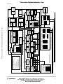

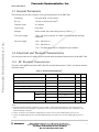

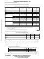

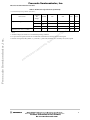

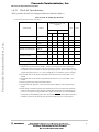
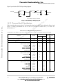


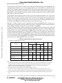
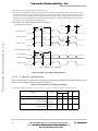

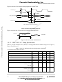
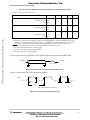
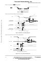
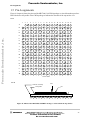
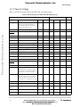
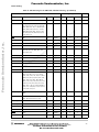

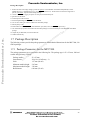
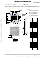
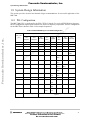

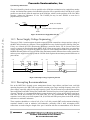
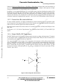
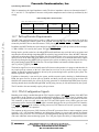

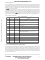
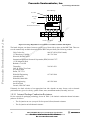
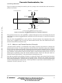
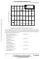


![PC755BM8 [Preliminary]](http://vs1.manualzilla.com/store/data/005786860_1-ac3ee01c2b00aeb18fc7f0a57a841c91-150x150.png)