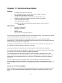
1
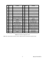
10623 Roselle Street, San Diego, CA 92121 y (858) 550-9559 y Fax (858) 550-7322 [email protected] y www.accesio.com MODEL 104-QUAD-8 USER MANUAL File: m104-quad-8.A1i Notice The information in this document is provided for reference only. ACCES does not assume any liability arising out of the application or use of the information or products described herein. This document may contain or reference information and products protected by copyrights or patents and does not convey any license under the patent rights of ACCES, nor the rights of others. IBM PC, PC/XT, and PC/AT are registered trademarks of the International Business Machines Corporation. Printed in USA. Copyright 2002, 2005 by ACCES I/O Products, Inc. 10623 Roselle Street, San Diego, CA 92121. All rights reserved. WARNING!! ALWAYS CONNECT AND DISCONNECT YOUR FIELD CABLING WITH THE COMPUTER POWER OFF. ALWAYS TURN COMPUTER POWER OFF BEFORE INSTALLING A BOARD. CONNECTING AND DISCONNECTING CABLES, OR INSTALLING BOARDS INTO A SYSTEM WITH THE COMPUTER OR FIELD POWER ON MAY CAUSE DAMAGE TO THE I/O BOARD AND WILL VOID ALL WARRANTIES, IMPLIED OR EXPRESSED. 2 Warranty Prior to shipment, ACCES equipment is thoroughly inspected and tested to applicable specifications. However, should equipment failure occur, ACCES assures its customers that prompt service and support will be available. All equipment originally manufactured by ACCES which is found to be defective will be repaired or replaced subject to the following considerations. Terms and Conditions If a unit is suspected of failure, contact ACCES' Customer Service department. Be prepared to give the unit model number, serial number, and a description of the failure symptom(s). We may suggest some simple tests to confirm the failure. We will assign a Return Material Authorization (RMA) number which must appear on the outer label of the return package. All units/components should be properly packed for handling and returned with freight prepaid to the ACCES designated Service Center, and will be returned to the customer's/user's site freight prepaid and invoiced. Coverage First Three Years: Returned unit/part will be repaired and/or replaced at ACCES option with no charge for labor or parts not excluded by warranty. Warranty commences with equipment shipment. Following Years: Throughout your equipment's lifetime, ACCES stands ready to provide on-site or inplant service at reasonable rates similar to those of other manufacturers in the industry. Equipment Not Manufactured by ACCES Equipment provided but not manufactured by ACCES is warranted and will be repaired according to the terms and conditions of the respective equipment manufacturer's warranty. General Under this Warranty, liability of ACCES is limited to replacing, repairing or issuing credit (at ACCES discretion) for any products which are proved to be defective during the warranty period. In no case is ACCES liable for consequential or special damage arriving from use or misuse of our product. The customer is responsible for all charges caused by modifications or additions to ACCES equipment not approved in writing by ACCES or, if in ACCES opinion the equipment has been subjected to abnormal use. "Abnormal use" for purposes of this warranty is defined as any use to which the equipment is exposed other than that use specified or intended as evidenced by purchase or sales representation. Other than the above, no other warranty, expressed or implied, shall apply to any and all such equipment furnished or sold by ACCES. 3 TABLE OF CONTENTS Chapter 1: Functional Description............................................................................... 5 Features ................................................................................................................................................... 5 Applications ............................................................................................................................................ 5 Figure 1-1: Block Diagram................................................................................................................... 7 Chapter 2: Installation................................................................................................... 8 Figure 2-1: PC/104 Key Information.................................................................................................... 9 Chapter 3: Option Selection ....................................................................................... 10 Figure 3-1: Option Selection Map...................................................................................................... 10 Chapter 4: Address Selection .................................................................................... 11 Chapter 5: Programming ............................................................................................ 12 Chapter 6: Connector Pin Assignments.................................................................... 16 Table 6-1: Connector Pin Assignments - P2 .................................................................................... 16 Table 6-2: Connector Pin Assignments - P3 .................................................................................... 17 4 Chapter 1: Functional Description Features 8 Quadrature Encoders are interfaced Input conditioning for each encoder allows us of a variety of encoders Interrupt Software Enabled for 8 encoders Interrupts are programmable for parameters such as speed or count Outputs to computer can include count, speed, direction of movement 24 bit counters for each encoder +5V Supply Available to the User. Compatible with Industry Standard I/O Racks like Gordos, Opto-22, Potter & Brumfield, etc. Applications Automatic Test Systems. Laboratory Automation. Robotics. Machine Control. Security Systems, Energy Management. The card is a general purpose Quadrature Encoder Counter/Interface board. It is provided in the popular 104 format and conditions and monitors the outputs of 8 encoders. These functions include anything that can be programmed into the versatile LSI/CSI LS7266R1 integrated circuit. These functions include speed, direction and total count. By providing these functions, it frees the computer for higher level applications. The ability to provide an interrupt for a parameter, such as total count, further frees the computer from the necessity of constantly reading the position of an encoder. Interrupts are directed to levels #2 through #7, #10 through #12, and #15 by jumper installation. The card is designed for industrial applications. Each input line is buffered and capable of utilizing inputs up to 25 volts. A +5 Volt source is available for appropriate encoders. The conditioned inputs are connected to appropriate LSI/CSI LS7266R1 integrated circuits. These circuits are the heart of the card’s operation. They may be programmed for a variety of functions. The programming is discussed later and the user is referred to the manufacturers data sheet for detailed information. The card occupies 32 bytes of I/O address space. The base address is selectable via jumpers anywhere within the range of 100-3E0 hex. An illustrated setup program is provided with the card. Interactive displays show locations and proper settings of jumpers to set up board address and interrupt levels. SPECIAL NOTE FOR PROGRAMMERS: The one language not recommended for programming interrupt service routines is any version of Visual BASIC. The recommended programming languages for IRQ based applications are Delphi and C++ Builder. 5 Specification Power Consumption + 5 Volts 260mA Input Section Receiver Type Configuration AM26LS32 Each encoder consists of Phase A Input, Phase B Input and Index Input, differential conditioning provided Number of Channels 8 Common mode input range +/- 7 V maximum Differential Input Range +/- 25 V maximum Input Sensitivity +/- 200 mV Input Hysteresis 50 mV Typical Input Impedance 12KΩ shunted by 150Ω in series with 4.7nF Input Options Resistive pull ups or pull downs may be specified Absolute maximum input differential +/- 25 V Counter Section Counter Type: Clock Frequency Separation Clock Pulse width Index Pulse width LS7266R1 24 bit Dual Axis Quadrature Counter 4.3 MHz maximum 57 ns min 115 ns min 85 ns min Clock Frequency Clock A - high pulse width Clock B - high pulse width Filter Clock (FCK) Digital Filter rate 30 MHz maximum 16 ns min 16 ns min Bus Clock (normally 8.33 MHz) (Optional Crystal available) Same as FCK Interrupt Controller Section Controller Type Interrupts Interrupt Sources Addressing CPLD Jumper selectable (2-7,10-12,15) All Carry/Borrow outputs from LS7266R1s All Index Inputs ISA bus address is set by jumpers 6 Environmental Operating Temperature: Storage Temperature: Humidity: 0 EC to +70 EC (optional -40 EC to +85 EC) -50 EC to +120 EC up to 95% RH, non-condensing Figure 1-1: Block Diagram 7 Chapter 2: Installation A printed Quick-Start Guide (QSG) is packed with the board for your convenience. If you’ve already performed the steps from the QSG, you may find this chapter to be redundant and may skip forward to begin developing your application. The software provided with this PC/104 Board is on CD and must be installed onto your hard disk prior to use. To do this, perform the following steps as appropriate for your operating system. Substitute the appropriate drive letter for your CD-ROM where you see d: in the examples below. CD Installation The following instructions assume the CD-ROM drive is drive “D”. Please substitute the appropriate drive letter for your system as necessary. DOS 1. Place the CD into your CD-ROM drive. 2. Type B- to change the active drive to the CD-ROM drive. 3. 4. Type GLQR?JJ- to run the install program. Follow the on-screen prompts to install the software for this board. WINDOWS 1. Place the CD into your CD-ROM drive. 2. The system should automatically run the install program. If the install program does not run promptly, click START | RUN and type BGLQR?JJ, click OK or press -. 3. Follow the on-screen prompts to install the software for this board. LINUX 1. Please refer to linux.htm on the CD-ROM for information on installing under linux. 8 Installing the Hardware Before installing the board, carefully read Chapter 3 and Chapter 4 of this manual and configure the board according to your requirements. The SETUP Program can be used to assist in configuring jumpers on the board. Be especially careful with Address Selection. If the addresses of two installed functions overlap, you will experience unpredictable computer behavior. To help avoid this problem, refer to the FINDBASE.EXE program installed from the CD. The setup program does not set the options on the board, these must be set by jumpers. To Install the Board 1. Install jumpers for selected options and base address according to your application requirements, as mentioned above. 2. Remove power from the PC/104 stack. 3. Assemble standoff hardware for stacking and securing the boards. 4. Carefully plug the board onto the PC/104 connector on the CPU or onto the stack, ensuring proper alignment of the pins before completely seating the connectors together. 5. Install I/O cables onto the board’s I/O connectors and proceed to secure the stack together or repeat steps 3-5 until all boards are installed using the selected mounting hardware. 6. Check that all connections in your PC/104 stack are correct and secure then power up the system. 7. Run one of the provided sample programs appropriate for your operating system that was installed from the CD to test and validate your installation. Figure 2-1: PC/104 Key Information 9 Chapter 3: Option Selection The only options to select on the card are the IRQ level and the card’s base address. All other options are selected via software. Interrupts are directed to levels #2 through #7, #10 through #12, and #15 by jumpers installed at locations labeled IRQ2 through IRQ7, IRQ10 through IRQ12, and IRQ15. IRQ 2 IRQ 3 IRQ 4 IRQ 5 IRQ 6 IRQ 7 IRQ 10 IRQ 11 IRQ 12 IRQ 15 A9 A8 A7 A6 A5 A4 Figure 3-1: Option Selection Map 10 Chapter 4: Address Selection The card occupies 16 bytes of I/O space. The card base address can be selected anywhere within the I/O address range 100-3E0 hex. If in doubt of where to assign the base address, refer to the table below and the FINDBASE program. HEX RANGE 000-00F 020-021 040-043 060-06F 070-07F 080-09F 0A0-0BF 0C0-0DF 0F0-0F1 0F8-0FF 170-177 1F0-1F8 200-207 238-23B 23C-23F 278-27F 2B0-2BF 2C0-2CF 2D0-2DF 2E0-2E7 2E8-2EF 2F8-2FF 300-30F 310-31F 320-32F 370-377 378-37F 380-38F 3A0-3AF 3B0-3BB 3BC-3BF 3C0-3CF 3D0-3DF 3E8-3EF 3F0-3F7 3F8-3FF USAGE 8237 DMA Controller 1 8259 Interrupt 8253 Timer 8042 Keyboard Controller CMOS RAM, NMI Mask Reg, RT Clock DMA Page Register 8259 Slave Interrupt Controller 8237 DMA Controller 2 Math Coprocessor Math Coprocessor Fixed Disk Controller 2 Fixed Disk Controller 1 Game Port Bus Mouse Alt. Bus Mouse Parallel Printer EGA EGA EGA GPIB (AT) Serial Port Serial Port Hard Disk (XT) Floppy Controller 2 Parallel Printer SDLC SDLC MDA Parallel Printer VGA EGA CGA Serial Port Floppy Controller 1 Serial Port Table 4-1: Hex Ranges 11 Chapter 5: Programming The card is an I/O-mapped device that is easily configured from any language and any language can easily perform quadrature reads. This is especially true if the form of the data is byte or word wide. All references to the I/O ports would be in absolute port addressing. However, a table could be used to convert the byte or word data ports to a logical reference. The languages Delphi and C++ Builder are recommended to program in to take advantage of the IRQ feature. With Visual C is more difficult to accomplish this, and Visual BASIC is NOT recommended for interrupt-type programming. Address Port Assignment Operation Base Address Channel 1 Data Read/Write Base Address +1 Channel 1 Command Read/Write Base Address +2 Channel 2 Data Read/Write Base Address +3 Channel 2 Command Read/Write Base Address +4 Channel 3 Data Read/Write Base Address +5 Channel 3 Command Read/Write Base Address +6 Channel 4 Data Read/Write Base Address +7 Channel 4 Command Read/Write Base Address +8 Channel 5 Data Read/Write Base Address +9 Channel 5 Command Read/Write Base Address +A Channel 6 Data Read/Write Base Address +B Channel 6 Command Read/Write Base Address +C Channel 7 Data Read/Write Base Address +D Channel 7 Command Read/Write Base Address +E Channel 8 Data Read/Write Base Address +F Channel 8 Command Read/Write Base Address +10 Interrupt Register Read Only Base Address +11 Channel Operation Register Write Only Base Address +12 Index/Interrupt Register Write Only Base Address +13 Select 128906.25 Hz FCK Write Only Base Address +14 Select 33MHz FCK Write Only Table 5-1: Base Address Information 12 Device First LS7266R1 Second LS7266R1 Third LS7266R1 Fourth LS7266R1 Data Registers (0, 2, 4, 8, A, C, E)h: These registers are read in order to retrieve the current count from the card, and written to in order to set the Preset Register. In order to read from any of the registers a write must first be performed on that data register’s corresponding control register. In order to get the count from Data register 0 you would first write 91h to the control register at address 1. Three reads are then required to get the current count from data register 0. The first read returns the Least Significant Byte and the last read returns the Most Significant Byte. In order to write to the Preset Register first write 91h to the control register. Then perform three writes to the data register. The first write is the Least Significant Byte, and the last write is the Most Significant Byte. Control Registers (1, 3, 5, 7, 9, B, D, F)h: The control registers all correspond to the data register that is one address below it. The control register is actually used for reading the FLAG register, using the Reset and Load Signal Decoders, setting up the Counter Mode Register, and setting up the Input/Output Control Register. Reading the Flag Register: Perform a single read from the control register. Bit 0/ BT: Borrow Toggle flip-flop Toggles every time the counter underflows. Bit 1/CT: Carry Toggle flip-flop. Toggles every time the counter overflows Bit 2/CPT : Compare Toggle flip-flop. Toggles every time the counter is equal to the Preset Register Bit 3/S: Sign flag. Set to 1 when counter underflows and reset to 0 when it overflows. Bit 4/E: Error flag. Set to 1 when excessive noise is present at the count inputs in quadrature mode. Ignore in other modes. Bit 5/U/D: Up/Down flag. Set to 1 when counting up and reset to 0 when counting down Bit 6//IDX: Index. Set to 1 when selected index input is at active level. Bit 7: Not used is always 0. The various registers are written to by using bits 5 and 6 of a one byte write to the control address. Using the Reset and Load Signal Decoders: Bit 0: 1 to reset BP Bits 1 & 2: set bit 1 high for reset CNTR, set bit 2 high for Reset BT, CT, CPT, S flags, set both bits high for reset E flag bits 3 & 4: set bit 3 high to transfer Preset Register to Counter. Set bit 4 high to transfer counter to output latch (so it can be read from the data address), set both bits high to transfer the LSB of the Preset Register to the Clock Prescaler. Bits 5&6: set both bits to 0 for the decoder. Bit 7: set high Writing to the Counter Mode Register: Bit 0: set low to use Binary Count, and set high to use BCD count. Bits 1 & 2: set both low to use normal count, set bit 1 high to use Range Limit, set bit 2 high to use NonRecycle Count, set both bits high to use Modulo-N count. Bits 3 & 4: set both bits low to use non-quadrature mode, set bit 3 high to use Quadrature times 1, set bit 4 high to use Quadrature times 2, and set both bits high to use Quadrature times 4. Bits 5& 6: set bit 5 high and bit 6 low in order to use the Counter Mode Register Bit 7: set high Writing to the Input/Output Control Register: Bits 0 & 1 & 2 : set low. Bits 3 & 4: set both bits low to set FLG1 to go high on a Carry. Set bit 3 high to set FLG1 to go high on a COMPARE. Set bit 4 high to set FLG1 to go high on a Carry or Borrow, and set both bits high to set FLG1 to go high whenever the FLAG register has bit 6 (IDX) set high. Note that when Interrupts are enabled on the card they occur whenever FLG1 is high. Bits 5 & 6: set bit 5 low and bit 6 high in order to use the Input/Output Control Register. Bit 7: set high 14 Manual 104-QUAD-8 Working with Interrupts: Channel Operation Register (11h) Bit 0: 0 sets all Counter CNTR/ABC inputs to 1 Bit 1: Reserved Bit 2: 1 enables the interrupt function using all Flag 1's for each channel Bits 3 through 7: Reserved To enable Interrupts on the card write 6h to address 11h. This will set the card to generate interrupts whenever FLG1 on any channel goes high as described in Writing to the Counter Mode Register. When an interrupt occurred read from address 10h to determine which bit. The Least Significant Bit will correspond to the first channel. Index/Interrupt Register (12h) This register is used to route the conditioned index input signals to the appropriate Counters, permitting the generation of index initiated interrupts. Each bit of this register controls the routing of one channel. Bit 0: Routes the index signal for Channel 1 Bit 1: Routes the index signal for Channel 2 Bit 2: Routes the index signal for Channel 3 Bit 3: Routes the index signal for Channel 4 Bit 4: Routes the index signal for Channel 5 Bit 5: Routes the index signal for Channel 6 Bit 6: Routes the index signal for Channel 7 Bit 7: Routes the index signal for Channel 8 15 Manual 104-QUAD-8 Chapter 6: Connector Pin Assignments Pin Channel 1 Function Pin Channel Function Ground 18 3 Fused +5V 2 1 Fused +5V 19 3 Index Negative Input 3 1 Index Negative Input 20 3 Index Positive Input 4 1 Index Positive Input 21 3 Quadrature A Negative Input 5 1 Quadrature A Negative Input 22 3 Quadrature A Positive Input 6 1 Quadrature A Positive Input 23 3 Quadrature B Negative Input 7 1 Quadrature B Negative Input 24 3 Quadrature B Positive Input 8 1 Quadrature B Positive Input 25 Ground 26 4 Fused +5V 9 Ground 10 2 Fused +5V 27 4 Index Negative Input 11 2 Index Negative Input 28 4 Index Positive Input 12 2 Index Positive Input 29 4 Quadrature A Negative Input 13 2 Quadrature A Negative Input 30 4 Quadrature A Positive Input 14 2 Quadrature A Positive Input 31 4 Quadrature B Negative Input 15 2 Quadrature B Negative Input 32 4 Quadrature B Positive Input 16 2 Quadrature B Positive Input 33 No connection Ground 34 No connection 17 Table 6-1: Connector Pin Assignments - P2 Note: When single-ended encoders are used, the signals should be connected to the positive inputs. 16 Manual 104-QUAD-8 Pin Channel 1 Function Pin Channel Function Ground 18 7 Fused +5V 2 5 Fused +5V 19 7 Index Negative Input 3 5 Index Negative Input 20 7 Index Positive Input 4 5 Index Positive Input 21 7 Quadrature A Negative Input 5 5 Quadrature A Negative Input 22 7 Quadrature A Positive Input 6 5 Quadrature A Positive Input 23 7 Quadrature B Negative Input 7 5 Quadrature B Negative Input 24 7 Quadrature B Positive Input 8 5 Quadrature B Positive Input 25 Ground 26 8 Fused +5V 9 Ground 10 6 Fused +5V 27 8 Index Negative Input 11 6 Index Negative Input 28 8 Index Positive Input 12 6 Index Positive Input 29 8 Quadrature A Negative Input 13 6 Quadrature A Negative Input 30 8 Quadrature A Positive Input 14 6 Quadrature A Positive Input 31 8 Quadrature B Negative Input 15 6 Quadrature B Negative Input 32 8 Quadrature B Positive Input 16 6 Quadrature B Positive Input 33 No connection Ground 34 No connection 17 Table 6-2: Connector Pin Assignments - P3 Note: When single-ended encoders are used, the signals should be connected to the positive inputs. 17 Manual 104-QUAD-8 Customer Comments If you experience any problems with this manual or just want to give us some feedback, please email us at: [email protected]. Please detail any errors you find and include your mailing address so that we can send you any manual updates. 10623 Roselle Street, San Diego CA 92121 Tel. (858)550-9559 FAX (858)550-7322 www.accesio.com 18 Manual 104-QUAD-8 Partner in Electronic Components & Supply Chain Solutions The Netherlands Denmark Elektrostraat 17 NL-7483 PG Haaksbergen Tel: +31 (0)53 573 33 33 Fax: +31 (0)53 573 33 30 [email protected] Marielundvej 46B DK-2730 Herlev Tel: +45 88 20 26 30 Fax: +45 88 20 26 39 [email protected] Belgium United Kingdom Gentsesteenweg 1154-C22 Chaussée de Gand 1154-C22 B-1082 Brussel / Bruxelles Tel: +32 (0)2 462 01 00 Fax: +32 (0)2 462 01 99 [email protected] St. Mary’s House, Church Lane Carlton Le Moorland Lincoln LN5 9HS Tel: +44 (0)1522 789 555 Fax: +44 (0)845 299 22 26 [email protected] Germany Germany Justus-von-Liebig-Ring 7-9 D-25451 Quickborn Tel: +49 (0)4106 627 07-0 Fax: +49 (0)4106 627 07-20 [email protected] Martin-Kollar-Strasse 9 D-81829 München Tel: +49 (0)89 436 086-0 Fax: +49 (0)89 436 086-19 [email protected] Austria Pyrkergasse 6/1 A-1190 Wien Tel: +43 (0)1 369 09 09 - 0 Fax: +43 (0)1 369 09 10 [email protected] Texim Europe B.V. Elektrostraat 17 Tel: +31 (0)53 573 33 33 [email protected] www.texim-europe.com