1
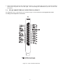
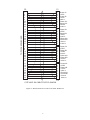
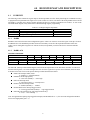
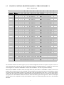
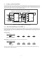
PCI-QUAD04 Four Channel Quadrature Encoder Input Board User’s Manual Revision 2 October, 2000 LIFETIME WARRANTY Every hardware product manufactured by Measurement Computing Corp. is warranted against defects in materials or workmanship for the life of the product, to the original purchaser. Any products found to be defective will be repaired or replaced promptly. LIFETIME HARSH ENVIRONMENT WARRANTYTM Any Measurement Computing Corp. product which is damaged due to misuse may be replaced for only 50% of the current price. I/O boards face some harsh environments, some harsher than the boards are designed to withstand. When that happens, just return the board with an order for its replacement at only 50% of the list price. Measurement Computing Corp. does not need to profit from your misfortune. By the way, we will honor this warranty for any other manufacture’s board that we have a replacement for! 30 DAY MONEY-BACK GUARANTEE Any Measurement Computing Corp. product may be returned within 30 days of purchase for a full refund of the price paid for the product being returned. If you are not satisfied, or chose the wrong product by mistake, you do not have to keep it. Please call for a RMA number first. No credits or returns accepted without a copy of the original invoice. Some software products are subject to a repackaging fee. These warranties are in lieu of all other warranties, expressed or implied, including any implied warranty of merchantability or fitness for a particular application. The remedies provided herein are the buyer’s sole and exclusive remedies. Neither Measurement Computing Corp., nor its employees shall be liable for any direct or indirect, special, incidental or consequential damage arising from the use of its products, even if Measurement Computing Corp. has been notified in advance of the possibility of such damages. MEGA-FIFO, the CIO prefix to data acquisition board model numbers, the PCM prefix to data acquisition board model numbers, PCM-DAS08, PCM-D24C3, PCM-DAC02, PCM-COM422, PCM-COM485, PCM-DMM, PCM-DAS16D/12, PCM-DAS16S/12, PCM-DAS16D/16, PCM-DAS16S/16, PCI-DAS6402/16, Universal Library, InstaCal, Harsh Environment Warranty and Measurement Computing Corp. are registered trademarks of Measurement Computing Corp. IBM, PC, and PC/AT are trademarks of International Business Machines Corp. Windows is a trademark of Microsoft Corp. All other trademarks are the property of their respective owners. Information furnished by Measurement Computing Corp. is believed to be accurate and reliable. However, no responsibility is assumed by Measurement Computing Corp. neither for its use; nor for any infringements of patents or other rights of third parties, which may result from its use. No license is granted by implication or otherwise under any patent or copyrights of Measurement Computing Corp. All rights reserved. No part of this publication may be reproduced, stored in a retrieval system, or transmitted, in any form by any means, electronic, mechanical, by photocopying, recording or otherwise without the prior written permission of Measurement Computing Corp. Notice Measurement Computing Corp. does not authorize any Measurement Computing Corp. product for use in life support systems and/or devices without the written approval of the President of Measurement Computing Corp. Life support devices/systems are devices or systems which, a) are intended for surgical implantation into the body, or b) support or sustain life and whose failure to perform can be reasonably expected to result in injury. Measurement Computing Corp. products are not designed with the components required, and are not subject to the testing required to ensure a level of reliability suitable for the treatment and diagnosis of people. (C) Copyright 2000, Measurement Computing Corporation HM PCI-QUAD04.lwp Table of Contents 1.0 INTRODUCTION . . . . . . . . . . . . . . . . . . . . . . . . . . . . . . . . . . . . . . . . . . . . . . . . . . . . . . . 1 2.0 SOFTWARE INSTALLATION . . . . . . . . . . . . . . . . . . . . . . . . . . . . . . . . . . . . . . . . . . . . 2 3.0 HARDWARE INSTALLATION . . . . . . . . . . . . . . . . . . . . . . . . . . . . . . . . . . . . . . . . . . . 3 3.1 SINGLE-ENDED/DIFFERENTIAL JUMPER SETTINGS . . . . . . . . . . . . . . . . . . . . . . 3 3.2 TERMINATION RESISTORS . . . . . . . . . . . . . . . . . . . . . . . . . . . . . . . . . . . . . . . . . . . . 3 3.3 BOARD INSTALLATION . . . . . . . . . . . . . . . . . . . . . . . . . . . . . . . . . . . . . . . . . . . . . . . 3 3.4 PCI-QUAD04 EXTERNAL CONNECTIONS & PINOUT . . . . . . . . . . . . . . . . . . . . . . 4 4.0 REGISTER MAP AND DESCRIPTIONS . . . . . . . . . . . . . . . . . . . . . . . . . . . . . . . . . . . . 6 4.1 OVERVIEW . . . . . . . . . . . . . . . . . . . . . . . . . . . . . . . . . . . . . . . . . . . . . . . . . . . . . . . . . . 6 4.1.1 BADR0 . . . . . . . . . . . . . . . . . . . . . . . . . . . . . . . . . . . . . . . . . . . . . . . . . . . . . . . . . . 6 4.1.2 BADR1+4Ch . . . . . . . . . . . . . . . . . . . . . . . . . . . . . . . . . . . . . . . . . . . . . . . . . . . . . . 6 4.2 CHANNEL CONTROL REGISTERS (BADR2 +0 THROUGH BADR2 +7) . . . . . . . . 7 4.2.1 Counter Mode Register (CMR) . . . . . . . . . . . . . . . . . . . . . . . . . . . . . . . . . . . . . . . . 8 4.2.2 Reset and Load Signal Decoders (RLD) . . . . . . . . . . . . . . . . . . . . . . . . . . . . . . . . . 9 4.2.3 Input/Output Control Register (IOR) . . . . . . . . . . . . . . . . . . . . . . . . . . . . . . . . . . . 10 4.2.4 Index Control Register (IDR) . . . . . . . . . . . . . . . . . . . . . . . . . . . . . . . . . . . . . . . . 11 4.3 GLOBAL CONTROL REGISTERS . . . . . . . . . . . . . . . . . . . . . . . . . . . . . . . . . . . . . . . 12 4.3.1 Index & Interrupt Routing Control (BADR2 + 8) . . . . . . . . . . . . . . . . . . . . . . . . . 12 4.3.2 Input Signal Control (BADR2 + 9) . . . . . . . . . . . . . . . . . . . . . . . . . . . . . . . . . . . 13 4.3.3 Programmable Interrupt Control Port A & B (BADR2 + 10 & 11) . . . . . . . . . . 13 5.0 SPECIFICATIONS . . . . . . . . . . . . . . . . . . . . . . . . . . . . . . . . . . . . . . . . . . . . . . . . . . . . . 14 This page is blank. 1.0 INTRODUCTION The PCI-QUAD04 is a PCI plug-in board that provides inputs and decoding for up to four incremental quadrature encoders. The PCI-QUAD04 can also be used as a high speed pulse counter for general counting applications. Incremental quadrature encoders are used to provide feedback signals from motors, that is, to count rotations and convert the physical movement into a series of electrical signals. These signals are sent to the computer which then decides whether or not to trigger signals that control the motor’s movement and what those control signals should be. The PCI-QUAD04 is the link between up to four incremental quadrature encoders and the computer. The PCI-QUAD04 is a plug-in board for PC/XT/AT computers; it uses one PCI slot and two rear panel openings for up to four channels. Each incremental quadrature encoder connects to an input channel on the board through a DB37 female connector on the board’s rear panel. Channels 1 through 4 connect to the DB37 connector on the rear panel bracket. For each channel, the signals provided at the DB37 connectors are: y y y y Phase A+, A− Phase B+, B− Index +/+5VDC and GND (optional power for +5V encoders) For pinout diagrams, refer to Section 3.5. The board provides inputs for three basic signals, Phase A, Phase B, and Index. Phase A and Phase B are generated at a 90° phase shift with respect to each other. Using these signals, a computer can determine system position (counts), velocity, (counts per second), and direction of rotation. The Index signal is used to establish an absolute reference position within one count of the encoder rotation (360°). Therefore, the Index signal is often used to reset or preset the position counter, particularly upon system startup when the incremental encoder can not determine the starting position of the motor. The Index signal can also be used to generate an interrupt signal to the computer. The Phase A, Phase B, and Index inputs are jumper-selectable for differential or single-ended input mode. These signals, after being routed through differential receivers, offer various paths to the LS7266 inputs through the FPGA. The inputs are register-selectable for: y y y y Individual incremental encoder inputs to allow up to four channels. Cascadable counters to allow non-quadrature counting up to 96 bits. Routing the Index input to either the Load Counter/Load Latch input or the Reset Counter/Gate input with quarter cycle and half cycle signals supported. Routing the Compare or Carry/Borrow output signals to the 8259 Interrupt controller. The heart of the PCI-QUAD04 is the LSI Computer Systems, Inc., LS7266R1 24-bit Dual-Axis Quadrature Counter IC. This component contains: y y y Two 24-bit counters with associated 24-bit preset and 24-bit output latch registers; Integrated digital filtering with 8-bit counter prescalers, Programmable index functionality and programmable count modes including non-quadrature modes. The board can also operate as a high-speed pulse and general purpose counter, cascadable to 96 bits. The 24-bit counters can count either in binary or BCD through register selection. The board also includes an 82C59 Programmable Interrupt Controller which accepts the four Index inputs directly and the Carry/Borrow outputs from the LS7266 (counter overflow/underflow or count value match) to generate interrupts to the PC bus. The interrupt controller operates in Polled Mode and allows for masking and priority setting of the interrupt inputs. For an overall view of PCI-QUAD04 functionality see Figure 1-1. 1 Figure 1-1. PCI-QUAD04 Functional Block Diagram 2.0 SOFTWARE INSTALLATION Before installing your board in the computer, you should install and run InstaCal. InstaCal is the installation, calibration and test software supplied with your data acquisition / IO hardware. It will guide you through the hardware settings for your board. These settings are also detailed in the following section. The complete InstaCal package is also included with the Universal Library. If you have ordered the Universal Library, use the Universal Library disk set to install InstaCal. The installation will create all required files and unpack the various pieces of compressed software. To install InstaCal, refer to the Software Installation Manual for complete instructions 2 3.0 HARDWARE INSTALLATION Before installing the board, configure the channels for either SINGLE-ENDED or DIFFERENTIAL operation. The channel configuration is established with a set of jumper blocks on the board. Each jumper is labeled for its functionality. Refer to section 3.1 following for details. 3.1 SINGLE-ENDED/DIFFERENTIAL JUMPER SETTINGS Prior to installation, set the jumpers on the PCI-QUAD04 to the positions required by your application. The PCI-QUAD04 is supplied preset for single-ended use with no termination resistors installed. Single-Ended Configuration (Default) Input Channel Insert Jumper From pin 2 to 3 (SE) Input 1 Phase A P3 Phase B P4 Index P5 2 P8 P7 P6 3 P14 P13 P12 4 P11 P10 P9 Differential Configuration Insert Jumper From pin 1 (DIFF) to 2 Input Phase A Phase B Index Input Channel 1 P3 P4 P5 2 P8 P7 P6 3 P14 P13 P12 4 P11 P10 P9 Figure 3-1. Example of Jumper Pin Numbering - SE/DIFF Jumpers 3.2 TERMINATION RESISTORS Although termination resistors typically are not required, SMT pads on the board have been left open, and labeled to allow the user to install terminating resistors from the various inputs to ground. Install Termination Resistors Input Phase A+ Phase APhase B+ Phase BIndex+ Index- 3.3 Channel 1 R9 R10 R11 R12 R14 R13 2 R22 R23 R20 R21 R19 R18 3 R38 R39 R36 R37 R35 R34 4 R30 R31 R28 R29 R27 R26 BOARD INSTALLATION 1. Turn the power off. 2. Remove the cover of your computer. Be careful not to dislodge any of the cables installed on the boards in your computer as you slide the cover off. 3. Locate an empty PCI expansion slot in your computer. 3 4. Push the board firmly down into the expansion bus connector. If it is not seated fully it may fail to work and could short circuit the PC bus power onto a PC bus signal. This could damage the motherboard in your PC as well as the PCI-QUAD. 3.4 PCI-QUAD04 EXTERNAL CONNECTIONS & PINOUT Pin assignments of the 37-pin connector, P2, are shown in Figure 3-2 below. Be sure to correctly phase the encoder according to the manufacturer’s instructions. Figure 3-2. 37-Pin Connector P2 Pin-Out 4 TO PCI-QUAD04 BOARD P5 P1 1 2 3 4 5 20 21 22 23 1 2 3 4 5 6 7 8 9 Phase 1A+5VDC Phase 1B+5VDC Index 1Phase 1A+ Phase 1B+ Ground Index 1+ 15 16 17 18 19 34 35 36 37 1 2 3 4 P2 5 6 7 8 9 Phase 2A+5VDC Phase 2B+5VDC Index 2Phase 2A+ Phase 2B+ Ground Index 2+ 7 8 9 10 24 25 26 27 28 1 2 3 4 5 6 7 8 9 Phase 3A+5VDC Phase 3B+5VDC Index 3Phase 3A+ Phase 3B+ Ground Index 3+ 1 2 3 4 5 6 7 8 9 Phase 4A+5VDC Phase 4B+5VDC Index 4Phase 4A+ Phase 4B+ Ground Index 4+ P3 11 12 13 14 29 30 31 32 33 P4 C37F-4X9F-1M CABLE FOR PCI-QUAD04 Figure 3-3. Board Connector-to-Cable C37F-4X9F-1M Pin Out 5 4.0 4.1 REGISTER MAP AND DESCRIPTIONS OVERVIEW The following section outlines the register map of the PCI-QUAD04 as well as briefly describing the commands necessary to program the PCI-QUAD04 at the register level (refer to Table 4-1 below). The heart of the PCI-QUAD04 is the LSI/CSI LS7266R1, a powerful device which is highly integrated to allow few external components to be needed. As seen in the LS7266R1 block diagram, many functions are controlled through register programming. Table 4-1. I/O Region Register Operations Function Operations PCI memory-mapped configuration registers 32-bit double word PCI I/O-mapped config. registers 32-bit double word Config & control registers 8-bit byte I/O Region BADR0 BADR1 BADR2 4.1.1 BADR0 BADR0 is reserved for the PLX-9052 configuration registers. There is no reason to access this region of I/O space for most PCI-DIO96 users. The installation procedure and Universal Library access all of the required information in this area. Unless you are writing direct register level software for the ,PCI-QUAD04 you will not need to be concerned with this address. 4.1.2 BADR1+4Ch INTCSR CONFIGURE 32:15 X 14 13 12 11 10 9 8 X X X X INTCLR X LEVEL/EDGE 7 6 5 4 3 2 1 0 X PCINT X X X INT INTPOL INTE READ/WRITE The INTCSR (Interrupt Control/Status Register) controls the interrupt features of the PLX-9052 controller. As with all of the PLX-9052 registers, it is 32-bits in length. Since the rest of the register have specific control functions, those bits must be masked off in order to access the specific interrupt control functions listed below. y INTE is the interrupt enable (local): 0 = disabled, 1 = enabled (default) y INTPOL is the interrupt polarity: 0 = active low (default), 1 = active high y INT is the interrupt status: 0 = interrupt not active, 1 = interrupt active y PCINT is the PCI interrupt enable: 0 = disabled (default), 1 = enabled y LEVEL/EDGE is the interrupt trigger control: 0 = level triggered mode (default), 1 = edge triggered mode y INTCLR is the interrupt clear (edge triggered mode only): 0 = N/A, 1 = clear interrupt Note: For applications requiring edge triggered interrupts (LEVEL/EDGE bit 8 = 1), the user must configure the INTPOL bit for active high polarity (bit 1=1). 6 4.2 CHANNEL CONTROL REGISTERS (BADR2 +0 THROUGH BADR2 +7) Table 4-1. Register Map P CI-QU AD0x R E GIS T E R MAP R egis ter P CI B AS E 2 + 0 P CI B AS E 2 + 1 P CI B AS E 2 + 2 P CI B AS E 2 + 3 P CI B AS E 2 + 4 P CI B AS E 2 + 5 P CI B AS E 2 + 6 P CI B AS E 2 + 7 P CI B AS E 2 + 8 P CI B AS E 2 + 9 P CI B AS E 2 + 10 P CI B AS E 2 + 11 RD WR RD WR WR WR WR WR WR WR WR RD WR RD WR WR WR WR WR WR WR WR RD WR RD WR WR WR WR WR WR WR WR RD WR RD WR WR WR WR WR WR WR WR RD WR RD WR RD WR RD WR RD D ata B its D7 D6 D5 D4 D3 D2 D1 D0 F unction D7 D6 D5 D4 D3 D2 D1 D0 Read Channel 1 OL byte s egment addres s ed by B P D7 D6 D5 D4 D3 D2 D1 D0 Write Channel 1 PR byte s egment addres s ed by B P 0 IDX U/D* E S CPT CT BT Read Channel 1 F L AG regis ter 0 0 0 *-------------- S E E L S 7266R1 S PEC ----------------- Write to Channel 1 RL D regis ter *-------------- S E E L S 7266R1 S PEC ----------------- Write to Channel 1 CMR regis ter 0 0 1 *-------------- S E E L S 7266R1 S PEC ----------------- Write to Channel 1 IOR regis ter 0 1 0 *-------------- S E E L S 7266R1 S PEC ----------------- Write to Channel 1 IDR regis ter 0 1 1 1 0 0 *-------------- S E E L S 7266R1 S PEC ----------------- Write to Channel 1 and 2 RL D regis ter 1 0 1 *-------------- S E E L S 7266R1 S PEC ----------------- Write to Channel 1 and 2 CMR regis ter *-------------- S E E L S 7266R1 S PEC ----------------- Write to Channel 1 and 2 IOR regis ter 1 1 0 *-------------- S E E L S 7266R1 S PEC ----------------- Write to Channel 1 and 2 IDR regis ter 1 1 1 D7 D6 D5 D4 D3 D2 D1 D0 Read Channel 2 OL byte s egment addres s ed by B P D7 D6 D5 D4 D3 D2 D1 D0 Write Channel 2 PR byte s egment addres s ed by B P 0 IDX U/D* E S CPT CT BT Read Channel 2 F L AG regis ter 0 0 0 *-------------- S E E L S 7266R1 S PEC ----------------- Write to Channel 2 RL D regis ter *-------------- S E E L S 7266R1 S PEC ----------------- Write to Channel 2 CMR regis ter 0 0 1 *-------------- S E E L S 7266R1 S PEC ----------------- Write to Channel 2 IOR regis ter 0 1 0 *-------------- S E E L S 7266R1 S PEC ----------------- Write to Channel 2 IDR regis ter 0 1 1 1 0 0 *-------------- S E E L S 7266R1 S PEC ----------------- Write to Channel 1 and 2 RL D regis ter 1 0 1 *-------------- S E E L S 7266R1 S PEC ----------------- Write to Channel 1 and 2 CMR regis ter 1 1 0 *-------------- S E E L S 7266R1 S PEC ----------------- Write to Channel 1 and 2 IOR regis ter *-------------- S E E L S 7266R1 S PEC ----------------- Write to Channel 1 and 2 IDR regis ter 1 1 1 D7 D6 D5 D4 D3 D2 D1 D0 Read Channel 3 OL byte s egment addres s ed by B P D7 D6 D5 D4 D3 D2 D1 D0 Write Channel 3 PR byte s egment addres s ed by B P 0 IDX U/D* E S CPT CT BT Read Channel 3 F L AG regis ter 0 0 0 *-------------- S E E L S 7266R1 S PEC ----------------- Write to Channel 3 RL D regis ter 0 0 1 *-------------- S E E L S 7266R1 S PEC ----------------- Write to Channel 3 CMR regis ter *-------------- S E E L S 7266R1 S PEC ----------------- Write to Channel 3 IOR regis ter 0 1 0 *-------------- S E E L S 7266R1 S PEC ----------------- Write to Channel 3 IDR regis ter 0 1 1 *-------------- S E E L S 7266R1 S PEC ----------------- Write to Channel 3 and 4 RL D regis ter 1 0 0 1 0 1 *-------------- S E E L S 7266R1 S PEC ----------------- Write to Channel 3 and 4 CMR regis ter 1 1 0 *-------------- S E E L S 7266R1 S PEC ----------------- Write to Channel 3 and 4 IOR regis ter *-------------- S E E L S 7266R1 S PEC ----------------- Write to Channel 3 and 4 IDR regis ter 1 1 1 D7 D6 D5 D4 D3 D2 D1 D0 Read Channel 4 OL byte s egment addres s ed by B P D7 D6 D5 D4 D3 D2 D1 D0 Write Channel 4 PR byte s egment addres s ed by B P 0 IDX U/D* E S CPT CT BT Read Channel 4 F L AG regis ter 0 0 0 *-------------- S E E L S 7266R1 S PEC ----------------- Write to Channel 4 RL D regis ter 0 0 1 *-------------- S E E L S 7266R1 S PEC ----------------- Write to Channel 4 CMR regis ter *-------------- S E E L S 7266R1 S PEC ----------------- Write to Channel 4 IOR regis ter 0 1 0 *-------------- S E E L S 7266R1 S PEC ----------------- Write to Channel 4 IDR regis ter 0 1 1 *-------------- S E E L S 7266R1 S PEC ----------------- Write to Channel 3 and 4 RL D regis ter 1 0 0 1 0 1 *-------------- S E E L S 7266R1 S PEC ----------------- Write to Channel 3 and 4 CMR regis ter 1 1 0 *-------------- S E E L S 7266R1 S PEC ----------------- Write to Channel 3 and 4 IOR regis ter 1 1 1 *-------------- S E E L S 7266R1 S PEC ----------------- Write to Channel 3 and 4 IDR regis ter CB INT 4 CB INT 3 CB INT 2 CB INT 1 IND4S EL IND3S EL IND2S EL IND1S EL Interrupt routing control regis ter CB INT 4 CB INT 3 CB INT 2 CB INT 1 IND4S EL IND3S EL IND2S EL IND1S EL N/A PH4B 1 PH4B 0 PH4A PH3B PH3A PH2B PH2A Input s ignal control regis ter (for cas cading counters ) N/A PH4B 1 PH4B 0 PH4A PH3B PH3A PH2B PH2A *-------------------- 8259 Programmable Interrupt Controller Port A ---------------------Programmable Interrupt Controller Port A *-------------------- 8259 Programmable Interrupt Controller Port A -----------------------* *-------------------- 8259 Programmable Interrupt Controller Port B -------------------- Programmable Interrupt Controller Port B *-------------------- 8259 Programmable Interrupt Controller Port B -----------------------* N/A N/A N/A N/A INT E INT 2 INT 1 INT 0 Interrupt s election regis ter The LS7266R1 contains two control registers per axis, and the configuration of each axis requires a sequence of writes to set the operating mode of the chip. The following description outlines the configuration steps for a single axis. The first axis control registers are contained at the BADR2 +0 address and at BADR2+1. The other axis perform identically. When read, the BADR2 +0 address returns the Output Latch (OL) data. Writes to the BADR2 +0 address set the Preset Register (PR). All register access to the LS7266R1 is done through byte wide operations. However, the PR and OL registers are 24-bits wide. The LS7266R1 contains a byte pointer that is auto-incremented after each write. To set the preset register requires three byte-wide writes (outport b), starting with the least significant byte. Be sure to reset the byte pointer prior to any register writes. The BADR2+1 address accesses the status and control registers for the given axis. There are four unique registers which can be configured by writing to the BADR2+1 register. For further details please also refer to the LS7266R1 data sheet. 7 At the BADR2 +1 location the four registers are uniquely selected for write access by the value in bits 5 and 6. The following table indicates the bit values for each register. Register Name Reset and Load (RLD) Count Mode (CMR) Input/Output Control (IOR) Index Control (IDR) Selected for Write Access by bits 5 & 6 x00x xxxx x01x xxxx x10x xxxx x11x xxxx If bit 7 is one (1) then the selected operation will effect both the X and Y channels. If bit 7 is zero then the X*/Y input is used to select the target channel. The remaining bits in each register are used to configure the LS7266R1 for various operating modes. The following sections describe how each register can be configured. It should be noted that in several instances there are bit fields that support multiple options. Obviously, only one option can be selected for each write operation, thus, it may be necessary to perform several writes to the same register to achieve the desired results. For example, to initialize the RLD register, that is, to clear all of the status flags and reset the counter, requires three separate writes to the register. Refer to the tables below for more details. 4.2.1 Counter Mode Register (CMR) The CMR contains three user-configurable fields, count representation, count mode, and quadrature scaling. Each field consists of one or more bits in the CMR register. After you select the desired mode, the bit fields need to be assembled into a byte that can be written to the CMR register. Bits 5 and 6 are always 1 and 0, respectively, for CMR register accesses. Data Encoding The quadrature count can be represented in either BCD or binary. Bit 0 of the CMR register selects the desired option. CMR Count Representation BINARY BCD Bit 0 Value for Count Configuration x01x xxx0 x01x xxx1 Count Mode There are four different count modes that are selected by bits 1 and 2. The count modes are Normal, Range-Limit, Non-recycle, and Modulo-N. CMR Count Mode Normal Range-Limit Non-recycle Modulo-N Bit 1 & 2 Value for Mode Selection x01x x00x x01x x10x x01x x01x x01x x11x Count Mode Definitions: y y y Range Limit: An upper limit, set by PR, and a lower limit, set to 0, are set. The CNTR stops at CNTR = PR when counting UP and when CNTR = 0 when counting DOWN. Counting resumed only when the count direction is reversed. Non-Recycle: CNTR is disabled whenever overflow or underflow happens. End-of-cycle marked by Carry (UP) or Borrow (DOWN). Re-enabled by reset or load on CNTR. Modulo-N: Count boundary set between 0 and content of PR. When counting up, at CNTR = PR, the CNTR is reset to 0 and the up count is continued from that point. When counting down, at CNTR = 0, the CNTR is loaded with content of PR and down count is continued from that point. Quadrature scaling There are four different scaling values that can be applied to quadrature signals: Non-quad, X1, X2, and X4. The scaling to be applied is set in bits 3 & 4 of the CMR register. Assuming the attached encoder generates 2500 pulses per revolution in 8 X1 mode, then you would receive 5000 pulses in X2 mode and 10,000 pulses in X4 mode. If the board will be used to detect simple clock pulses then select Non-Quadrature mode. CMR Quadrature Scaling Non-Quadrature X1 X2 X4 4.2.2 Bit 3 & 4 value for quad scaling x010 0xxx x010 1xxx x011 0xxx x011 1xxx Reset and Load Signal Decoders (RLD) The RLD contains three user configurable fields. This register controls all of the reset options as well as the data transfer options. The following sections describe each field in the RLD register and the various modes that can be set for operation. The RLD register is used to reset the counter and the status flags and also to provide access to the error bit E, which is the only means for resetting this flag once it is set. RLD Reset Byte Pointer Field This field is used to reset the byte pointer. The byte pointer is auto-incremented each time the Output Latch (OL) register is read or the Preset Register (PR) is written to. The byte pointer must be reset prior to any access to the 24-bit counter register. RLD Byte Pointer Reset NOP BP Reset Bit 0 value for byte pointer reset x00x xxx0 x00x xxx1 RLD Reset Fields In addition to the byte pointer there are several other fields that can be reset. This field provides the mechanism for resetting the counter and all of the status flags. The Borrow Toggle (BT), Carry Toggle (CT), Compare Toggle (CPT), and the Sign Flag (S) can all be reset through bits 1 and 2 of the RLD register. Finally, the only way to clear the Error (E) flag once it has been set is through the RLD register. RLD Reset NOP CNTR BT, CT, CPT, and S E Bit 1 & 2 value for reset fields x00x x00x x00x x01x x00x x10x x00x x11x 9 RLD Transfer Fields The final bit field in the RLD register consists of bits 3 and 4. This field controls the data transfer operation of the LS7266 chip. There are three options that are available as listed in the table below. The contents of the Preset Register can be transferred to the Counter, the contents of the Counter can be copied to the Output Latch for reading, and the Preset Register contents can be copied to the Filter Clock Prescalar. This register provides the software mechanism for reading the current count from the encoder. First write to the RLD register to transfer the contents of the counter to the output latch, then reset the byte pointer and perform three reads of the output latch. RLD Transfer NOP Preset to Counter Counter to Output Latch Preset to Filter Clock Prescalar 4.2.3 Bit 3 & 4 value for transfer fields x000 0xxx x000 1xxx x001 0xxx x001 1xxx Input/Output Control Register (IOR) The IOR register contains four user configurable fields and should be initialized prior to writing the IDR register which follows. The IOR register, in conjunction with the IDR register, configures how the A and B input signals are interpreted. A/B configuration bit This configuration bit controls whether or not the A and B inputs are enabled or disabled. This bit must be enabled for the counter to respond to input clock pulses. IOR A/B enable/disable Disable A and B Enable A and B Bit 0 value for enable/disable x10x xxx0 x10x xxx1 LCNTR/LOL Pin Configuration This register is only applicable if the IDR register bit 2 is set to 0. In this case the Index input from the external encoder is directed to the LCNTR/LOL pin. This bit then configures the operation of the LCNTR/LOL pin. The operation can be set to either load the counter with the preset value or load the output latch input. Thus, if the IDR register specifies the Load CNTR operation, then each time the Index input is asserted, the counter will be reloaded with the value stored in the preset. If the Load OL input option is selected, then each Index input will cause the current counter value to be updated to the Output Latch. In this mode you are not required to use the RLD register to force the contents of the counter to be copied to the output latch. The contents of the counter will automatically be available at the Output Latch every time the Index signal is asserted. Note: the Index input is asserted once per revolution. IOR LCNTR/LOL pin configuration Load CNTR Load OL input Bit 1 value for CNTR/LOL select x10x xx0x x10x xx1x RCNTR/ABG Pin Configuration This bit configures the operation of the RCNTR/ABG pin. This register in only applicable if the IDR register bit 2 is set to 1. In this mode the Index input from the encoder is directed to the RCNTR/ABG input. The operation can be configured to either reset the CNTR input or as an A/B enable gate. Note: in non-quadrature mode this register should be set for A/B enable gate operation. IOR RCNTR/ABG pin configuration Reset CNTR A/B enable gate Bit 2 value for RCNTR/ABG select x10x x0xx x10x x1xx FLAG 1 & 2 Configuration This bit field controls the operation of the FLG1 and FLG2 real-time counter outputs. The selected configuration will determine what signal is output on the FLG1 and FLG2 output pins. For cascading the counters this register should be set for Carry/Borrow, Up/Down operation. The FLGx output pins are also redirected to the onboard 8259 Programmable Interrupt 10 Controller (PIC). Depending on how the FLGx register is configured an interrupt can be generated based on the options in the following table. IOR FLG1/FLG2 configuration FLG1 Carry, FLG2 Borrow FLG1 Compare, FLG2 Borrow FLG1 Carry/Borrow, FLG2 U/D FLG1 IDX, FLG2 is E 4.2.4 Bit 3 & 4 value for FLG1/FLG2 select x100 0xxx x100 1xxx x101 0xxx x101 1xxx Index Control Register (IDR) The IDR register controls how the Index input from the encoder should be treated; it contains three user-configurable fields. The polarity and Index routing selection are also made through this register. Note: Disable indexing for non-quadrature inputs. Enable/Disable Index This bit is used to select whether or not indexing is enabled for the LS7266. IDR Index enable/disable Disable Index Enable Index Bit 0 value for enable/disable select x11x xxx0 x11x xxx1 Index Polarity Select If your are connecting a quadrature encoder, then this bit selects the polarity for the index: 0 for negative polarity and 1 for positive polarity. IDR Index Polarity Negative Index Polarity Positive Index Polarity Bit 1 value for Index Polarity select x11x xx0x x11x xx1x Index Pin Select The final bit field in the IDR register determines where the index input will be connected. A 0 in this field will select the LCNTR/LOL pin as the connection for the encoder index output. If the field is set to 1, then the RCNTR/ABG pin is selected as the index input. Prior to configuring this field the IOR register bit 1 or 2 must be configured. See the previous section for more details on these bit fields. IDR Index Pin Select LCNTR/LOL pin is indexed RCNTR/ABG pin is indexed Bit 2 value for Index Pin select x11x x0xx x11x x1xx 11 4.3 GLOBAL CONTROL REGISTERS Four global control registers are located at offsets 8-11 from the BADR2 address. The following sections outline these four registers and the various control functionality which they provide. Unlike the channel configuration registers, the current state of the global control registers can be obtained through reading the desired register. To help understand registers and functions, refer to Figure 4-1 below as you read the register descriptions. Counter Cascading Functional Diagram 1A 1A 1B FLG1 3A 1 PH3A 3A 0 3B 1 PH3B 3B 0 4A 1 PH4A 4A 0 4B 10 01 00 1B PH2A 2A FLG2 2A 1 0 2B 1 PH2B 2B 0 LS7266 FLG3 FLG4 4B LS7266 PH4AB1/B0 Figure 4-1. Cascade Counting Functional Diagram 4.3.1 Index & Interrupt Routing Control (BADR2 + 8) The first four bits of this register route the index pin from the quadrature encoder to either the LCNTR/LOL input or the RCNTR/ABG input for each of the four encoder inputs. The value set in this register should be consistent with the value written in the IDR register. The most significant four bits select the interrupt source as either Compare select or Carry/Borrow select. Interrupt Routing: Register BADR2 + 8 D4-D7 Channel Input FLG1 - Carry/Compare/Index FLG2 - Borrow/UP/Down 1 CBINT1 0 1 2 CBINT2 0 1 3 CBINT3 0 1 4 CBINT4 0 1 Index Routing: Connects the index input to the counter control input pin below. Register BADR2 + 8 D0-D3 Channel Input RCNTR/ABG LCNTR/LOL 1 IND1SEL 0 1 2 IND2SEL 0 1 3 IND3SEL 0 1 4 IND4SEL 0 1 *The FLG1 and FLG2 output pins are register programmable for Carry, Borrow, Compare and flag status functions. (See 7266 IOR register for proper functionality) 12 4.3.2 Input Signal Control (BADR2 + 9) Controls Counter Cascading: (Non-quadrature mode) Set the FLGx pin for the CARRY/BORROW function through the IOR Register bits 3 and 4 so that the cascaded direction output will be CARRY for UP counting and BORROW for DOWN counting. Register BADR2 + 9 D0-D6 (4) 24-bit counters (1/2/3/4) (2) 48-bit counters (1-2/3-4) (1) 24-bit/1 - 72bit (1/2-3-4) (1) 96-bit counter (1-2-3-4) PH2A 0 1 0 1 PH2B 0 1 0 1 PH3A 0 0 1 1 PH3B 0 0 1 1 PH4A 0 1 1 1 PH4B1/PH4B0 0,0 1,0 0,1 0,1 Defaults to 0x00 (no inter-counter connections). 4.3.3 Programmable Interrupt Control Port A & B (BADR2 + 10 & 11) The PCI-QUAD04 uses an 8259A Programmable Interrupt Controller which routes up to eight interrupts from the Index inputs or Carry/Borrow outputs (due to overflow, underflow, or compare match, depending on strap setting and register programming) from the LS7266's. The interrupt output from the 8259 is routed through the FPGA and register enabled and set to IRQ 2, 3, 5, 7, 10, 11, 12, or 15 on the PC bus. Each interrupt can be masked to prevent unwanted interrupt generation through 8259 programming. The 8259A can only be used in non-vectored x86/x88 mode, or polled mode. That is, when an interrupt is generated, the user must poll the 8259A to determine which interrupt was set. This mode is set externally by setting: INTA* (pin 26) connected to +5VDC SP\EN (pin 16) connected to 10kohm pullup to +5VDC CAS0:2 (pins 12,13,15) connected to 10kohm pullup to +5VDC For programming and further information on the 8259A interrupt controller, consult an Intel Peripheral Components 1992 data book (or Harris 8259A data sheet). 13 5.0 SPECIFICATIONS All Specifications typical for 25°C unless otherwise specified. Power consumption (Not supplying power to external encoders) +5V 325 mA typical, 460 mA max. (Typical supplying 1 Dynamics Research Incremental Optical Rotary Encoder part number M21AAFOBB2E-2500) +5V 1058 mA typical, 1479 mA max. Input section Receiver type Configuration Differential Single-Ended Number of channels Common mode input voltage range Differential input voltage range Input sensitivity Input hysteresis Input impedance Propagation delay Absolute maximum input voltage Differential Miscellaneous SN75ALS175 quad differential receiver Each channel consists of PhaseA input, PhaseB input and Index input. Each input is jumper-selectable as single-ended or differential PhaseA, PhaseB and Index (+) inputs at user connector routed to (+) inputs of differential receiver. PhaseA, PhaseB and Index (−) inputs at user connector routed to (−) inputs of differential receiver. PhaseA, PhaseB and Index (+) inputs at user connector routed to (+) inputs of differential receiver. PhaseA, PhaseB and Index (−) inputs at user connector routed to ground. (−) inputs of differential receiver routed to +3V reference. 4 ±12V max. ±12V max. ±200mV 50mV typ. 12 kohm min. 27 ns max. (tpLH, tpHL) ±14V max. Meets or exceeds ANSI EIA/TIA-422-B, EIA/TIA-423-B, RS-485. Meets ITU recommendations V.10, V.11, X.26, X.27. Designed for multipoint busses on long lines and in noisy environments. 14 Counter section Counter type LS7266R1 24-bit Dual-axis Quadrature Counter Quadrature Mode Clock frequency Separation Clock pulse width Index pulse width 4.3 MHz max. 57 ns min. 115 ns min. 85 ns min. Count Mode Clock frequency Clock A - high pulse width Clock A - low pulse width 30 MHz max, (25 MHz max Mod-N mode) 14 ns min. 14 ns min. Filter clock (FCK) Digital filter rate 10 MHz 10 MHz, software selectable divider (1 to 256 in single steps) Crystal oscillator (FCK source) Frequency Frequency accuracy 10 MHz 100 ppm Interrupt Controller Section Controller type Configuration Interrupts Interrupt enable Interrupt polarity Interrupt sources 8259 Programmable Interrupt Controller Polled mode only INTA# - mapped to IRQn via PCI BIOS at boot-time Programmable through PLX9052 INTCSR High or low level. Programmable through PLX9052 Rising / falling edge. Programmable through PLX-9052 All Carry/Borrow outputs from LS7266R1, all Index inputs Environmental Operating temerature range Storage temerature range Humidity 0 to 70°C −40 to 100°C 0 to 90% non-condensing 15 For your notes 16 EC Declaration of Conformity We, Measurement Computing Corporation, declare under sole responsibility that the product: PCI-QUAD04 Four-Channel Incremental Quadrature Encoder Board Part Number Description to which this declaration relates, meets the essential requirements, is in conformity with, and CE marking has been applied according to the relevant EC Directives listed below using the relevant section of the following EC standards and other normative documents: EU EMC Directive 89/336/EEC: Essential requirements relating to electromagnetic compatibility. EU 55022 Class B: Limits and methods of measurements of radio interference characteristics of information technology equipment. EN 50082-1: EC generic immunity requirements. IEC 801-2: Electrostatic discharge requirements for industrial process measurement and control equipment. IEC 801-3: Radiated electromagnetic field requirements for industrial process measurements and control equipment. IEC 801-4: Electrically fast transients for industrial process measurement and control equipment. Carl Haapaoja, Director of Quality Assurance Measurement Computing Corporation 16 Commerce Boulevard, Middleboro, Massachusetts 02346 (508) 946-5100 Fax: (508) 956-9500 E-mail: [email protected] www. measurementcomputing.com