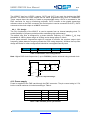
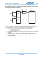
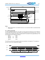
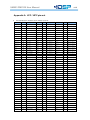
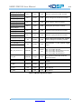
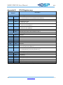
1
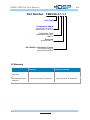
UM023 FMC230 User Manual r1.4 FMC230 User Manual 4DSP, USA. Email: [email protected] This document is the property of 4DSP LLC. and may not be copied nor communicated to a third party without the written permission of 4DSP LLC. © 4DSP LLC. 2014 UM023 www.4dsp.com -1- UM023 FMC230 User Manual r1.4 Revision History Date Description Revision 2012-12-19 Release 1.0 2013-02-05 Corrected pin assignments in Appendix A 1.1 2013-03-22 Updated analog output range in Table 2 and added a FMC700 requirement information for KC705 1.2 2013-08-15 Updated analog output bandwidth in Table 2. Added a signal description in Appendix A. 1.3 2014-01-30 Removed the wrongful reference to analog input gain and over range in chapter 2 1.4 UM023 www.4dsp.com -2- UM023 FMC230 User Manual r1.4 Table of Contents 1 Acronyms and related documents ................................................................................ 4 1.1 Acronyms ................................................................................................................... 4 1.2 Related Documents .................................................................................................... 4 2 General description ........................................................................................................ 5 3 Installation ...................................................................................................................... 5 3.1 Requirements and handling instructions ..................................................................... 5 4 Design ............................................................................................................................. 6 4.1 Physical specifications ............................................................................................... 6 4.1.1 Board Dimensions ............................................................................................... 6 4.1.2 Front panel .......................................................................................................... 6 4.2 Electrical specifications .............................................................................................. 6 4.2.1 EEPROM ............................................................................................................ 6 4.2.1 FMC Connector ................................................................................................... 6 4.2.1 JTAG................................................................................................................... 7 4.3 Main characteristics.................................................................................................... 7 4.4 Analog output channels .............................................................................................. 8 4.5 External trigger input .................................................................................................. 8 4.6 External clock input .................................................................................................... 9 4.7 External reference input ............................................................................................. 9 4.8 External clock output .................................................................................................. 9 4.9 Clock tree ................................................................................................................... 9 4.9.1 PLL design ........................................................................................................ 10 4.10 Power supply ........................................................................................................ 10 5 Controlling the FMC230................................................................................................ 11 5.1 Architecture .............................................................................................................. 11 5.2 SPI Programming ..................................................................................................... 13 6 Environment.................................................................................................................. 15 6.1 Temperature ............................................................................................................ 15 6.2 Monitoring ................................................................................................................ 15 6.3 Cooling ..................................................................................................................... 15 6.3.1 Convection cooling ............................................................................................ 15 6.3.2 Conduction cooling ............................................................................................ 16 7 Safety............................................................................................................................. 16 8 EMC ............................................................................................................................... 16 9 Ordering information .................................................................................................... 16 10 Warranty ........................................................................................................................ 17 Appendix A LPC / HPC pin-out ........................................................................................ 18 Appendix B CPLD Register map ..................................................................................... 21 UM023 www.4dsp.com -3- UM023 FMC230 User Manual r1.4 1 Acronyms and related documents 1.1 Acronyms ADC DDR DSP EPROM FBGA FMC FPGA JTAG LED LVTTL LSB LVDS MGT MSB PCB PCI PCIe PLL PMC PSSR QDR SDRAM SRAM TTL XMC Analog to Digital Converter Double Data Rate Digital Signal Processing Erasable Programmable Read-Only Memory Fineline Ball Grid Array FPGA Mezzanine Card Field Programmable Gate Array Join Test Action Group Light Emitting Diode Low Voltage Transistor Logic level Least Significant Bit(s) Low Voltage Differential Signaling Multi-Gigabit Transceiver Most Significant Bit(s) Printed Circuit Board Peripheral Component Interconnect PCI Express Phase Locked Loop PCI Mezzanine Card Power Supply Rejection Ratio Quadruple Data rate Synchronous Dynamic Random Access memory Synchronous Random Access memory Transistor Logic level PCIe Mezzanine card Table 1: Glossary 1.2 Related Documents FPGA Mezzanine Card (FMC) standard ANSI/VITA 57.1-2010 Datasheet AD9129, Rev C, Analog Devices Datasheet AD9517 Rev A, Analog Devices Datasheet AD7291 Rev B, Analog Devices FMC700 User Manual, 4DSP UM023 www.4dsp.com -4- UM023 FMC230 User Manual r1.4 2 General description The FMC230 is a two channel DAC FMC daughter card. The card provides two 14-bit up to 5.6GSPS DAC channels which can be clocked by an internal clock source (optionally locked to an external reference) or an externally supplied sample clock. There is one trigger input for customized sampling control. The FMC daughter card is mechanically and electrically compliant to FMC standard (ANSI/VITA 57.1). The FMC has a high-pin count connector, front panel I/O, and can be used in a conduction cooled environment. The design is based on Analog Devices AD9129 single channel 14-bit 5.6GSPS DAC with DDR LVDS inputs. The analog output signals are AC coupled connecting to MMCX coax connectors on the front panel. The FMC allows flexible control on sampling frequency through serial communication busses. Furthermore the card is equipped with power supply and temperature monitoring and offers several power-down modes to switch off unused functions or protect the card from overheating. Monitoring Ref Clock Sample Clock Clock Tree Clock Status & Control Clock Output DAC A AD9129 single channel 14-bit, 5.6 GSPS DAC B AD9129 single channel DDR LVDS Status & Control FMC Connector HPC 400 Pins Trigger DDR LVDS Status & Control 14-bit, 5.6 GSPS Figure 1: FMC230 block diagram 3 Installation 3.1 Requirements and handling instructions Prevent electrostatic discharges by observing ESD precautions when handling the card. Do not flex the card. The FMC daughter card must be installed on a carrier card compliant to the FMC standard. The FMC carrier card must support the high-pin count connector (400-pins) to support all channels. A low-pin count connector is supported but may result in limited features. The FMC carrier card may support a VADJ/VIO_B voltage of +1.2V to +3.3V. The FMC700 is required in order to use the FMC230 on KC705. UM023 www.4dsp.com -5- UM023 FMC230 User Manual r1.4 4 Design 4.1 Physical specifications 4.1.1 Board Dimensions The FMC card complies with the FMC standard known as ANSI/VITA 57.1. The card is a single width conduction cooled mezzanine module (with region 1 and front panel I/O). There may be a mechanical conflict with the front rib on a carrier card. The stacking height is 10mm and the PCB thickness is 1.6mm. 4.1.2 Front panel There are 10 MMCX connectors available from the front panel. From top to bottom; - Analog outputs B (D1) and A (D0) - Trigger in (TR) - Clock Input (CI) - Reference Input (RI) - Clock Output (CO) A3 A2 A1 A0 D1 D0 TR CI RI CO Figure 2: Front panel layout 4.2 Electrical specifications The DAC devices use DDR LVDS signals mapped to the regular FMC pins. Each channel has two 14-bit wide DDR LVDS busses. Control signals operate in LVCMOS mode. A VADJ range of 1.2V to 3.3V is supported. The voltage on VIO_B pins will follow the voltage on VADJ. The CLKx pins are required to be LVDS by the FMC standard. CLK2 and CLK3 are not used for best compatibility with Xilinx development platforms. CLK0 is connected to a spare clock output of the clock tree. CLK1 is connected to the external trigger. 4.2.1 EEPROM The FMC card carries a small serial EEPROM (M24C02) which is accessible from the carrier card through the I2C bus. The EEPROM is powered by 3P3VAUX. The standby current is only 0.01µA when SCL and SDA are kept at 3P3VAUX level. These signals may also be left floating since pull-up resistors are present on the FMC. By default the EEPROM is writeprotected. 4.2.1 UM023 FMC Connector www.4dsp.com -6- UM023 FMC230 User Manual r1.4 FMC Top Connector The top connector is the main connector to the FMC carrier board. The pin-out is defined in the appendix. The connector is a HPC connector. FMC Bottom Connector The high-pin count connector enables FMC card stacking. The following connections are available between the top and bottom FMC connector: Unused gigabit data signals (DP[4..9]_M2C_P/N, DP[0..9]_C2M_P/N). All gigabit reference clocks (GBTCLK[0..1]_M2C_P/N). RES0 3P3VAUX, 3P3V, 12P0V, VADJ JTAG (see section 4.2.1) The bottom connector is not mounted by default. 4.2.1 JTAG In a stacked environment the TDI pin will be decoupled from the TDO pin by the PRST_M2C_L signal coming from the bottom connector. TRST#, TCK, TMS, TDI and TDO are directly connected between top to bottom connector. Bottom connector (to stacked FMC) TRST# TCK TDI TMS TDO PRSNT_M2C_L TDO PRSNT_M2C_L 3P3V OE CPLD TRST# TCK TMS TDI Top connector (to FMC carrier) Figure 3: JTAG Connection 4.3 Main characteristics Analog outputs Number of channels 2 Channel resolution 14-bit Output voltage range Output impedance Analogue output bandwidth UM023 1.75 Vpp (9 dBm) 50Ω 1.4GHz, please refer to AD9129 datasheet for details www.4dsp.com -7- UM023 FMC230 User Manual r1.4 External sampling clock input 0dBm typical (LVTTL level supported) Input Level Input impedance 50Ω Input RF transformer: 4.5 MHz to 3000 MHz (AC coupled) Input range External reference clock input 0dBm typical (LVTTL level supported) Input Level Input impedance 50Ω 1MHz to 250MHz (AC coupled) Input range External clock output 800mVp-p into 50Ω typical (LVCMOS output available as build option, contact 4DSP) Output Level External Trigger input LVTLL/LVCMOS33 Logic ‘0’ max 0.8V / Logic ‘1’ min 2.0V Format Frequency range Up to 300 MHz Internal sampling clock LVPECL Format Frequency Range DAC: up to 5300MHz (Software selectable, contact 4DSP for frequencies higher frequencies up to 5600MHz) Table 2 : FMC daughter card main characteristics 4.4 Analog output channels The DAC output circuit is constructed such different build options can be made. The default configuration will be a wideband balun ETC1-1-13 (MACOM; 4.5 to 3000MHz). Please contact 4DSP for custom configurations. Figure 4: Wideband balun output option 4.5 External trigger input An external trigger is available on the front panel (MMCX connector). The trigger signal connects to a buffer (NB6N11S) before being sent to the carrier card. The buffer translates the external LVTTL signal to LVDS and connects to the FMC connector. The trigger input is terminated to ground with 4.7kΩ. UM023 www.4dsp.com -8- UM023 FMC230 User Manual 4.6 r1.4 External clock input There is one MMCX clock input on the front panel that can serve as sampling clock input. Refer also to section 4.9 for more information about the clock tree. Note: when internal clock is enabled and there is no need for an external reference; it is highly recommended to leave the clock input unconnected to prevent interference with the internal clock. 4.7 External reference input There is one MMCX reference input on the front panel that can serve as reference clock input. Refer also to section 4.9 for more information about the clock tree. Note: when internal clock is enabled and there is no need for an external reference; it is highly recommended to leave the reference input unconnected to prevent interference with the internal clock. 4.8 External clock output There is one MMCX clock input on the front panel that can serve as sampling/reference clock output. Refer also to section 4.9 for more information about the clock tree. 4.9 Clock tree The FMC offers a clock architecture that combines flexibility and high performance. Components have been chosen in order to minimize jitter and phase noise to reduce degradation of the data conversion performance. The user may choose to use an external sampling clock or an internal sampling clock. The clock tree has a PLL and clock distribution section. The PLL ensures locking of the internal VCO clock to an external supplied reference. There is an onboard reference which is used in case there is no external reference present. The onboard reference is a QuartzCom TX3-801 30.72MHz. Loop Filter REF_EN TCXO 30.72MHz Ref Clock DAC 0 DAC 1 To FMC To GBT To OUT Figure 5: Clock tree UM023 www.4dsp.com -9- UM023 FMC230 User Manual r1.4 The AD9517 has four LVPECL outputs. OUT2 and OUT3 are used for clocking the DAC devices. The other four clock outputs can be either programmed as LVDS or LVCMOS33. These outputs have the ability to enable a programmable delay. OUT4 is connected to the FMC connector for test en monitoring purposes. OUT5 connect to the gigabit transceiver reference clock on the FMC connector (as a build option it can be connected to OUT7). OUT6 connects to the clock output on a MMCX connector. 4.9.1 PLL design The PLL functionality of the AD9517 is used to operate from an internal sampling clock. To enable flexibility in frequency selection while maintaining high performance. The default loop filter is designed for a phase detector frequency of 7.68MHz (fref/4), loop bandwidth of 10KHz, phase margin of 45 deg, and a charge pump of 4.8mA. Lower phase detector frequencies might be required to achieve the required output clock frequency (phase detector frequency equals the VCO tuning step size). Whether the loop filter design still works for other configurations should be investigated case by case. Card Type FMC230 Device VCO Range VCO DAC Clock AD9517-1 2300MHz - 2650MHz 2457.60MHz 2457.60MHz Table 3: FMC default clock configurations Note: Higher DAC clock frequencies (fs up to 5600MHz) can be achieved using external clock. 8 LF 11 CP 4 C1 CLK 12 330pF /CLK Bypass 9 R1 1.00k R2 2.00k C2 4.70nF C3 150pF V Supply 220nF AD9517-X V+ F out 48 REFIN 47 Gnd /REFIN LD /OUT 0 Reference 30.7MHz 4.10 Power supply OUT 1 46 CP Rset 2 42 6: Loop filter design Figure OUT 0 /OUT 1 OUT 2 41 39 38 19 Power is supplied toCPRset the FMC card/OUTthrough the FMC connector. The pin current rating is 2.7A, 20 5.10k 2 22 but the overall maximum is limited OUT according to Table 4. 3 /OUT 3 44 Rset OUT 4 Rset Voltage /OUT 4 4.12k +3.3V +12V VADJ VIO_B (VADJ) OUT 5 /OUT 5 OUT 6 /OUT 6 OUT 7 /OUT 7 23 35 34 33 32 26 27 28 29 # Pins Max Amps Max Watt 4 2 4 2 3A 1A 4A 1.15 A 10 W 12 W 10 W 2.3 W Notes AD9517: 1. Consult manufacturer's data sheet for full details Table 4: FMC standard power specification UM023 www.4dsp.com - 10 - UM023 FMC230 User Manual r1.4 The power provided by the carrier card can be very noisy. Special care is taken with the power supply generation on the FMC card to minimize the effect of power supply noise on clock generation and data conversion. Clean +1.8V is derived from +3.3V with linear regulators. Clean +3.3V is derived from +12V in two steps for maximum efficiency. The first step uses a high efficient switched regulator to generate a +3.8V power rail. From this power rail each analog supply is derived with separate low dropout, low noise, linear regulators. The regulators have sufficient copper area to dissipate the heat in combination with proper airflow (see section 6.3 Cooling). ADP2301 45mW (Eff. 85%) 22mA @ 12V ADP7182 48mW 120mA @ -1.5V Max. 200mA 330mA @ 1.8Vd 175mA @ 1.8Va 60mA @ -1.5Va AD9129 850mW 330mA @ 1.8Vd 175mA @ 1.8Va 60mA @ -1.5Va AD9129 850mW ADP151 8mW 25mA @ 3.3V TCXO TX3-801 ADP1753 135mW 455mA @ 3.3V AD9517 1.5W ADP151 263mW Total Power Consumption: +/- 5.6W ADP1753 990mW 660mA @ 1.8V Max. 800mA ADP151 263mW 1010mA @ VADJ* 1010mA @ 3.3V** * VADJ may be used when 2.5V to save power consumption. ** 3.3V is the factory default assembly to cover most FMC carrier hardware. 169 mA @ 12V Selected by assembly ADP2301 406mW (Eff. 85%) 480mA @ 3.6V Max. 800mA Figure 7: Power supply tree Power plane VADJ 3P3V 12P0V 3P3VAUX (Operating) 3P3VAUX (Standby) Typical 0.2A + IVIO_B 1.0A 0.2A 0.1 mA 0.01 µA Maximum 1.1A 0.3A 3 mA 1 µA Table 5: Typical / Maximum current drawn from FMC carrier card 5 Controlling the FMC230 5.1 Architecture The data interface of one DAC channel occupies 31 differential pairs on the FMC connector. Since one DAC channel is available on the LPC connections, there are only 6 signals left on the LPC connections to control the board. Therefore the FMC will be controlled from a single SPI interface connecting to an onboard CPLD (Xilinx Coolrunner-II XC2C64A-QFG). Four connections are available between the FMC connector and the CPLD. The CPLD acts as a UM023 www.4dsp.com - 11 - UM023 FMC230 User Manual r1.4 SPI distribution device and level translator and comes factory programmed. The two remaining signals on the FMC connector are reserved. 3.3V VADJ CPLD FMC Connector ADG3304 4 Signals to: AD9517 Signals to: AD9129 4 FMC_TO_CPLD[3..0] 3.3V BANK 1.8V BANK Figure 8: FMC control interface The FMC is controlled from the carrier hardware through a single SPI communication bus. The SPI communication bus is connected to a CPLD which has the following tasks: Distribute SPI access from the carrier hardware along the local devices: - 2x AD9129 (D/A converters) - 1x AD9517 (Clock Tree) Enable/disable internal reference based on a SPI command from the carrier hardware (REF_EN). Generate SPI reset for AD9517 (CLK_N_RESET) and both AD9129 (DAC_RST) Collect local status signals and store them in a register which can be accessed from the carrier hardware. Drive a LED according to the level of the status signals. UM023 www.4dsp.com - 12 - UM023 FMC230 User Manual r1.4 Local Side CPLD FMC Side DAC0_N_CS DAC1_N_CS CLK_N_CS FMC_TO_CPLD(0) SCLK FMC_TO_CPLD(1) N_CS FMC_TO_CPLD(2) SDIO SCLK SDIO Shift register REF_EN SRC_SEL DAC_RST CLK_N_RESET Ctrl REG0 REG1 REG2 REFMON LD STATUS FMC_TO_CPLD(3) N_INT AND ALERT LED Figure 9: CPLD architecture Notes: SDO on the AD9517 and AD9129 devices is not connected. SDIO is used bidirectional (3-wire SPI). 5.2 SPI Programming The SPI programmable devices on the FMC can be accessed as described in their datasheet, but each SPI communication cycle needs to be preceded with a pre-selection byte. The preselection byte is used by the CPLD to forward the SPI command to the right destination. The pre-selection bytes are defined as follows: - CPLD 0x00 - AD9129 #1 0x82 - AD9129 #2 0x83 - AD9517 0x84 The CLPD has three internal registers which are described in the Appendix. The registers of the other devices are transparently mapped. N_CS SCLK SDIO P7 P6 P5 P4 P3 P2 P1 8-bit pre-selection P0 R/W A6 A5 A4 A3 A2 8-bit instruction A1 A0 D7 D6 D5 D4 D3 D3 D1 D0 8-bit register data Figure 10: Write instruction to CPLD registers A1:A0 UM023 www.4dsp.com - 13 - UM023 FMC230 User Manual r1.4 N_CS SCLK SDIO P7 P6 P5 P4 P3 P2 P1 P0 R/W A6 8-bit pre-selection A5 A4 A3 A2 A1 A0 D7 D6 8-bit instruction D5 D4 D3 D3 D1 D0 D1 D0 D1 D0 8-bit register data Figure 11: Read instruction to CPLD registers A1:A0 N_CS SCLK SDIO P7 P6 P5 P4 P3 P2 P1 P0 R/W N1 8-bit pre-selection N0 A4 A3 A2 A1 A0 D7 D6 8-bit instruction D5 D4 D3 D3 8-bit register data Figure 12: Write instruction to AD9129 registers A4:A0 N_CS SCLK SDIO P7 P6 P5 P4 P3 P2 P1 8-bit pre-selection P0 R/W N1 N0 A4 A3 A2 A1 A0 D7 D6 8-bit instruction D5 D4 D3 D3 8-bit register data Figure 13: Read instruction to AD9129 registers A4:A0 N_CS SCLK SDIO P7 P6 P5 P4 P3 P2 P1 8-bit pre-selection P0 R/W W1 W0 A12 A11 A10 A9 A8 A7 A6 A5 A4 A3 A2 A1 A0 D7 D6 16-bit instruction D5 D4 D3 D3 D1 D0 D1 D0 8-bit register data Figure 14: Write instruction to AD9517 registers A12:A0 N_CS SCLK SDIO P7 P6 P5 P4 P3 P2 P1 8-bit pre-selection P0 R/W W1 W0 A12 A11 A10 A9 A8 A7 A6 16-bit instruction A5 A4 A3 A2 A1 A0 D7 D6 D5 D4 D3 D3 8-bit register data Figure 15: Read instruction to AD9517 registers A12:A0 UM023 www.4dsp.com - 14 - UM023 FMC230 User Manual r1.4 6 Environment 6.1 Temperature Operating temperature -40°C to +85°C (Industrial) Storage temperature: -40°C to +120°C 6.2 Monitoring The FMC holds an AD7291 device for monitoring several power supply voltages on the board as well as temperature. The device can be programmed and read out through the I 2C bus. Continuously operating the I2C bus might interfere with the conversion process resulting in signal distortion. It is recommended to program the minimum and maximum limits in the monitoring devices and only read from the devices when the interrupt line is asserted. It is recommended that the carrier card and/or host software uses the power-down features in the case the temperature is too high. Parameter: Device 1 address 010 1111 (GA=00) address 010 1100 (GA=01) address 010 0011 (GA=10) address 010 0000 (GA=11) Formula External VIN0 1.8Va DAC VIN0 * 1 External VIN1 1.8Vd DAC VIN1 * 1 External VIN2 1.8Va VIN2 * 1 External VIN3 1.8Vd VIN3 * 1 External VIN4 3V3 CLK VIN4 * 2 External VIN5 3V3 TCXO VIN5 * 2 External VIN6 VADJ VIN6 * 2 External VIN7 -1V5 3.3 - 2 * VIN7 On-chip temperature Table 6: Temperature and voltage parameters 6.3 Cooling Two different types of cooling will be available for the FMC. 6.3.1 Convection cooling The air flow provided by the chassis fans the FMC is enclosed in will dissipate the heat generated by the on board components. A minimum airflow of 300 LFM is recommended. UM023 www.4dsp.com - 15 - UM023 FMC230 User Manual r1.4 For standalone operations (such as on a Xilinx development kit), it is highly recommended to blow air across the FMC and ensure that the temperature of the devices is within the allowed range. 4DSP’s warranty does not cover boards on which the maximum allowed temperature has been exceeded. 6.3.2 Conduction cooling In demanding environments, the ambient temperature inside a chassis could be close to the operating temperature defined in this document. It is very likely that in these conditions the junction temperature of power consuming devices will exceed the operating conditions recommended by the devices manufacturers (mostly +85°C). While a low profile heat sink coupled with sufficient air flow might be sufficient to maintain the temperature within operating boundaries, some active cooling would yield better results and would certainly help with resuming operations much faster in the case the devices were disabled because of a temperature “over range”. 7 Safety This module presents no hazard to the user. 8 EMC This module is designed to operate from within an enclosed host system, which is built to provide EMC shielding. Operation within the EU EMC guidelines is not guaranteed unless it is installed within an adequate host system. This module is protected from damage by fast voltage transients originating from outside the host system which may be introduced through the system. 9 Ordering information UM023 www.4dsp.com - 16 - UM023 FMC230 User Manual r1.4 Part Number: FMC230-2-1-1-1 Card Type Temperature Range Industrial (-40oC to +85oC) = 1 Commercial (0oC to +70oC) = 2 Connector Type MMCX (Standard feature) = 1 SSMC = 2 Reserved Standard Feature = 1 Mil-I-46058c Conformal Coating No Conformal Coating = 1 Add Conformal Coating = 2 10 Warranty Hardware Software/Firmware Basic Warranty (included) 1 Year from Date of Shipment 90 Days from Date of Shipment Extended Warranty (optional) 2 Years from Date of Shipment 1 Year from Date of Shipment UM023 www.4dsp.com - 17 - UM023 FMC230 User Manual r1.3 Appendix A LPC / HPC pin-out Note that FMC700 is required to use the FMC230 on KC705 AV57.1 HPC Pin FMC230 Signal AV57.1 HPC Pin FMC230 Signal AV57.1 HPC Pin FMC230 Signal CLK0_M2C_N H5 CLK_TO_FPGA_N HA00_N_CC F5 DAC1_DCO_N HB00_N_CC K26 DAC1_P1_DP05_N CLK0_M2C_P H4 CLK_TO_FPGA_P HA00_P_CC F4 DAC1_DCO_P HB00_P_CC K25 DAC1_P1_DP05_P CLK1_M2C_N G3 EXT_TRIGGER_N HA01_N_CC E3 DAC1_DCI_N HB01_N J25 DAC1_P1_DP04_N CLK1_M2C_P G2 EXT_TRIGGER_P HA01_P_CC E2 DAC1_DCI_P HB01_P J24 DAC1_P1_DP04_P CLK2_BIDIR_N K5 N.C. HA02_N K8 DAC1_FRM_N HB02_N F23 DAC1_P1_DP03_N CLK2_BIDIR_P K4 N.C. HA02_P K7 DAC1_FRM_P HB02_P F22 DAC1_P1_DP03_P CLK3_BIDIR_N J3 N.C. HA03_N J7 DAC1_P0_DP00_N HB03_N E22 DAC1_P1_DP02_N CLK3_BIDIR_P J2 N.C. HA03_P J6 DAC1_P0_DP00_P HB03_P E21 DAC1_P1_DP02_P LA00_N_CC G7 DAC0_DCO_N HA04_N F8 DAC1_P0_DP01_N HB04_N F26 DAC1_P1_DP01_N LA00_P_CC G6 DAC0_DCO_P HA04_P F7 DAC1_P0_DP01_P HB04_P F25 DAC1_P1_DP01_P LA01_N_CC D9 DAC0_DCI_N HA05_N E7 DAC1_P0_DP02_N HB05_N E25 DAC1_P1_DP00_N LA01_P_CC D8 DAC0_DCI_P HA05_P E6 DAC1_P0_DP02_P HB05_P E24 DAC1_P1_DP00_P LA02_N H8 DAC0_FRM_N HA06_N K11 DAC1_P0_DP04_N HB06_N_CC K29 DAC1_P1_DP06_N LA02_P H7 DAC0_FRM_P HA06_P K10 DAC1_P0_DP04_P HB06_P_CC K28 DAC1_P1_DP06_P LA03_N G10 DAC0_P0_DP00_N HA07_N J10 DAC1_P0_DP03_N HB07_N J28 DAC1_P1_DP07_N LA03_P G9 DAC0_P0_DP00_P HA07_P J9 DAC1_P0_DP03_P HB07_P J27 DAC1_P1_DP07_P LA04_N H11 DAC0_P0_DP01_N HA08_N F11 DAC1_P0_DP05_N HB08_N F29 DAC1_P1_DP09_N LA04_P H10 DAC0_P0_DP01_P HA08_P F10 DAC1_P0_DP05_P HB08_P F28 DAC1_P1_DP09_P LA05_N D12 DAC0_P0_DP02_N HA09_N E10 DAC1_P0_DP06_N HB09_N E28 DAC1_P1_DP08_N LA05_P D11 DAC0_P0_DP02_P HA09_P E9 DAC1_P0_DP06_P HB09_P E27 DAC1_P1_DP08_P LA06_N C11 DAC0_P0_DP03_N HA10_N K14 DAC1_P0_DP09_N HB10_N K32 DAC1_P1_DP11_N LA06_P C10 DAC0_P0_DP03_P HA10_P K13 DAC1_P0_DP09_P HB10_P K31 DAC1_P1_DP11_P LA07_N H14 DAC0_P0_DP04_N HA11_N J13 DAC1_P0_DP08_N HB11_N J31 DAC1_P1_DP10_N LA07_P H13 DAC0_P0_DP04_P HA11_P J12 DAC1_P0_DP08_P HB11_P J30 DAC1_P1_DP10_P LA08_N G13 DAC0_P0_DP05_N HA12_N F14 DAC1_P0_DP07_N HB12_N F32 DAC1_P1_DP13_N LA08_P G12 DAC0_P0_DP05_P HA12_P F13 DAC1_P0_DP07_P HB12_P F31 DAC1_P1_DP13_P LA09_N D15 DAC0_P0_DP06_N HA13_N E13 DAC1_P0_DP10_N HB13_N E31 DAC1_P1_DP12_N LA09_P D14 DAC0_P0_DP06_P HA13_P E12 DAC1_P0_DP10_P HB13_P E30 DAC1_P1_DP12_P LA10_N C15 DAC0_P0_DP09_N HA14_N J16 DAC1_P0_DP11_N HB14_N K35 LA10_P C14 DAC0_P0_DP09_P HA14_P J15 DAC1_P0_DP11_P HB14_P K34 LA11_N H17 DAC0_P0_DP08_N HA15_N F17 DAC1_P0_DP12_N HB15_N J34 LA11_P H16 DAC0_P0_DP08_P HA15_P F16 DAC1_P0_DP12_P HB15_P J33 LA12_N G16 DAC0_P0_DP07_N HA16_N E16 DAC1_P0_DP13_N HB16_N F35 LA12_P G15 DAC0_P0_DP07_P HA16_P E15 DAC1_P0_DP13_P HB16_P F34 LA13_N D18 DAC0_P0_DP10_N HA17_N_CC K17 HB17_N_CC K38 LA13_P D17 DAC0_P0_DP10_P HA17_P_CC K16 HB17_P_CC K37 LA14_N C19 DAC0_P0_DP13_N HA18_N J19 HB18_N J37 LA14_P C18 DAC0_P0_DP13_P HA18_P J18 HB18_P J36 LA15_N H20 DAC0_P0_DP12_N HA19_N F20 HB19_N E34 LA15_P H19 DAC0_P0_DP12_P HA19_P F19 HB19_P E33 LA16_N G19 DAC0_P0_DP11_N HA20_N E19 HB20_N F38 LA16_P G18 DAC0_P0_DP11_P HA20_P E18 HB20_P F37 LA17_N_CC D21 DAC0_P1_DP00_N HA21_N K20 HB21_N E37 LA17_P_CC D20 DAC0_P1_DP00_P HA21_P K19 HB21_P E36 UM023 FMC230 User Manual LA18_N_CC r1.4 C23 DAC0_P1_DP01_N HA22_N J22 LA18_P_CC C22 DAC0_P1_DP01_P HA22_P J21 LA19_N H23 DAC0_P1_DP03_N HA23_N K23 LA19_P H22 DAC0_P1_DP03_P HA23_P K22 LA20_N G22 DAC0_P1_DP02_N LA20_P G21 DAC0_P1_DP02_P LA21_N H26 DAC0_P1_DP05_N LA21_P H25 DAC0_P1_DP05_P LA22_N G25 DAC0_P1_DP04_N LA22_P G24 DAC0_P1_DP04_P LA23_N D24 DAC0_P1_DP06_N LA23_P D23 DAC0_P1_DP06_P LA24_N H29 DAC0_P1_DP10_N LA24_P H28 DAC0_P1_DP10_P LA25_N G28 DAC0_P1_DP09_N LA25_P G27 DAC0_P1_DP09_P LA26_N D27 DAC0_P1_DP07_N LA26_P D26 DAC0_P1_DP07_P LA27_N C27 DAC0_P1_DP08_N LA27_P C26 DAC0_P1_DP08_P LA28_N H32 DAC0_P1_DP12_N LA28_P H31 DAC0_P1_DP12_P LA29_N G31 DAC0_P1_DP11_N LA29_P G30 DAC0_P1_DP11_P LA30_N H35 DAC0_P1_DP13_N LA30_P H34 DAC0_P1_DP13_P LA31_N G34 FMC_TO_CPLD(1) LA31_P G33 FMC_TO_CPLD(0) CLK_DIR B1 LA32_N H38 FMC_TO_CPLD(3) PG_C2M D1 PG_C2M LA32_P H37 FMC_TO_CPLD(2) PG_M2C F1 PG_M2C LA33_N G37 I2C_SCL C30 I2C_SCL LA33_P G36 I2C_SDA C31 I2C_SDA Table 7: FMC230 Pinout Signal DAC0_DCO_P Group Direction I/O standard D/A 0 Output LVDS Clock coming from the 1st D/A converter. D/A 0 Input LVDS Clock going the 1st D/A converter. D/A 0 Input LVDS Frame going the 1st D/A converter. D/A 0 Input LVDS Data bus 0 going the 1st D/A converter. Description DAC0_DCO_N DAC0_DCI_P DAC0_DCI_N DAC0_FRM_P DAC0_FRM_N DAC0_P0_P<13..0> DAC0_P0_N<13..0> UM023 www.4dsp.com - - 19 UM023 FMC230 User Manual DAC0_P1_P<13..0> DAC0_P1_N<13..0> DAC1_DCO_P DAC1_DCO_N DAC1_DCI_P DAC1_DCI_N DAC1_FRM_P DAC1_FRM_N DAC1_P0_P<13..0> DAC1_P0_N<13..0> r1.4 D/A 0 Input LVDS Data bus 1 going the 1st D/A converter. D/A 1 Output LVDS Clock coming from the 2nd D/A converter. D/A 1 Input LVDS Clock going the 2nd D/A converter. D/A 1 Input LVDS Frame going the 2nd D/A converter. D/A 1 Input LVDS Data bus 0 going the 2nd D/A converter. D/A 1 Input LVDS Data bus 1 going the 2nd D/A converter. I/O Output LVDS Clock coming from the clock tree. Typically used for debug and monitoring purposes. I/O Output LVDS Representation of the external trigger signal. DAC1_P1_P<13..0> DAC1_P1_N<13..0> CLK_TO_FPGA_P CLK_TO_FPGA_N EXT_TRIGGER_P EXT_TRIGGER_N SPI bus to CPLD on the FMC176: FMC_TO_CPLD(0): SPI Clock FMC_TO_CPLD(1): SPI Chip Select (low active) FMC_TO_CPLD(2): SPI Data In/Out FMC_TO_CPLD(3): SPI Alert/Interrupt FMC_TO_CPLD<3..0> CONTROL Bidir CMOS VIO CLK_DIR CONTROL Output LVTTL CLK_DIR is not connected. CLK2 and CLk3 are unused. PG_C2M STATUS Input LVTTL Power good indicator from carrier to module. PG_M2C STATUS Output LVTTL Power good indicator from module to carrier. I2C_SCL I2C Input LVTTL I2C clock line. I2C_SDA I2C Bidir LVTTL I2C data line. Table 8: FMC230 Signal Description UM023 www.4dsp.com - - 20 UM023 FMC230 User Manual Appendix B r1.4 CPLD Register map Description Register 0x00 Control register 0 Bit 0 ‘0’ for internal reference clock ‘1’ for external reference clock (disable internal reference) Bit 1 Reserved Bit 2 ‘0’ Release DAC reset ‘1’ Assert DAC reset Bit 3 ‘0’ Release CLK reset (AD9517) ‘1’ Assert CLK reset (AD9517) Bit 4 ‘0’ Release CLK sync (AD9517) ‘1’ Assert CLK sync (AD9517) Bit 6..5 Bit 7 0x01 Reserved EEPROM write enable. Recommended to write ‘0’. Control register 1 Bit 0 Reserved R/O Bit 1 Reserved R/O Bit 2 Reserved Bit 3 Reserved R/O Bit 4 Reserved R/O Bit 5 Reserved Bit 6 ‘0’ for CLK power enable (AD9517) ‘1’ for CLK power down (AD9517) Bit 7 ‘0’ for MONITORING power enable (AD7291 rst_l) ‘1’ for MONITORING power down (AD7291 rst_l) 0x02 Status register Bit 0 REFMON (AD9517) Bit 1 LD (AD9517) Bit 2 STATUS (AD9517) Bit 3 ALERT (AD7291) Bit 4 IRQ (DAC) Bit 7..5 CPLD revision (current = b’001’) Table 9: CPLD Register Map UM023 www.4dsp.com - - 21