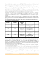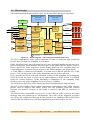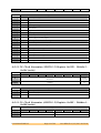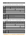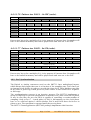
1
Sundance Multiprocessor Technology Limited
User Manual
Form : QCF42
Date : 6 July 2006
Unit / Module Description:
Dual 2.3GHz DAC PXI Express Module
Unit / Module Number:
SMT712
Document Issue Number:
5
Issue Date:
11/12/2012
Original Author:
PhSR
User Manual
for
SMT712
Sundance Multiprocessor Technology Ltd, Chiltern House,
Waterside, Chesham, Bucks. HP5 1PS.
This document is the property of Sundance and may not be copied
nor communicated to a third party without prior written
permission.
© Sundance Multiprocessor Technology Limited 2006
User Manual SMT712
Last Edited: 11/12/2012 10:36:00
Revision History
Issue
Changes Made
Date
Initials
1
Original Document released.
02/06/09
PhSR
2
DAC synchronisation function added
01/07/09
PhSR
3
FPGA Design supports xlinks
22/05/10
PhSR
4
Soft Reset added
15/07/10
PhSR
5
Updated for FX100T, SHB phase synchronisation
11/12/12
JV
User Manual SMT712
Page 2 of 89
Last Edited: 11/12/2012 10:36:00
Table of Contents
1
2
3
Introduction ........................................................................................................................ 8
Related Documents........................................................................................................... 9
Acronyms, Abbreviations and Definitions..............................................................10
3.1 Acronyms and Abbreviations ...................................................................................10
4
Functional Description ..................................................................................................10
4.1 General Block Diagram...............................................................................................10
4.2 Block Diagram – Standard SMT712 (PXIe)..............................................................11
4.3 Block Diagram – SMT712-HYBRPXI32 (option 32-bit PXI) ..................................12
4.4 Block Diagram – SMT712-CPCI32 (Option 32-bit PCI).........................................13
4.5 Module Description.....................................................................................................13
4.5.1 DACs..........................................................................................................................13
4.5.2 FPGA ..........................................................................................................................14
4.5.2.1 General Description......................................................................................14
4.5.2.2 Resources used – XCV5FX70T....................................................................14
4.5.2.3 Resources used – XCV5FX100T. ................................................................15
4.5.3 Configuration (CPLD+Flash).................................................................................17
4.5.4 DDR2 Memory .........................................................................................................19
4.5.5 Clock circuitry .........................................................................................................19
4.5.6 Data (samples) path / Data storage....................................................................20
4.5.7 PXI Express Bus .......................................................................................................21
4.5.8 SHB connector .........................................................................................................23
4.5.9 External Trigger. .....................................................................................................23
4.5.10Power dissipation ...................................................................................................24
4.5.11JTAG ..........................................................................................................................24
4.5.12PXI Express Hybrid Connectors...........................................................................26
4.6 FPGA Design .................................................................................................................28
4.6.1 Control Registers ....................................................................................................29
4.6.1.1 Register Descriptions ...................................................................................32
4.6.1.1.1 General Control Register – 0x08 (read-only). ..................................32
4.6.1.1.2 Set Control Register – 0x10 (write). ...................................................35
4.6.1.1.3 DACA (MAX19692) Register 0x1 – Configuration Register – 0x44
(write).
37
4.6.1.1.4 DACB (MAX19692) Register 0x1 – Configuration Register – 0x48
(write).
37
4.6.1.1.5 DACA and B data source selection – 0x4C (write). ........................38
4.6.1.1.6 Clock Generator (AD9516-2) Register 0x00 – Serial Port
Configuration – 0xC0 (write)...................................................................................38
4.6.1.1.7 Clock Generator (AD9516-2) Register 0x04 – Read-back Control –
0XC4 (write). ...............................................................................................................39
4.6.1.1.8 Clock Generator (AD9516-2) Register 0x10 – PFD and Charge
Pump – 0xC8 (write)..................................................................................................39
4.6.1.1.9 Clock Generator (AD9516-2) Register 0x11 – R Counter – 0xCC
(write).
40
User Manual SMT712
Page 3 of 89
Last Edited: 11/12/2012 10:36:00
4.6.1.1.10 Clock Generator (AD9516-2) Register 0x12 – R Counter – 0xD0
(write).
40
4.6.1.1.11 Clock Generator (AD9516-2) Register 0x13 – A Counter – 0xD4
(write).
41
4.6.1.1.12 Clock Generator (AD9516-2) Register 0x14 – B Counter – 0xD8
(write).
41
4.6.1.1.13 Clock Generator (AD9516-2) Register 0x15 – B Counter – 0xDC
(write).
41
4.6.1.1.14 Clock Generator (AD9516-2) Register 0x16 – PLL Control 1 –
0xE0 (write). ................................................................................................................42
4.6.1.1.15 Clock Generator (AD9516-2) Register 0x17 – PLL Control 2 –
0xE4 (write). ................................................................................................................43
4.6.1.1.16 Clock Generator (AD9516-2) Register 0x18 – PLL Control 3 –
0xE8 (write). ................................................................................................................44
4.6.1.1.17 Clock Generator (AD9516-2) Register 0x19 – PLL Control 4 –
0xEC (write). ................................................................................................................45
4.6.1.1.18 Clock Generator (AD9516-2) Register 0x1A – PLL Control 5 –
0xF0 (write). ................................................................................................................46
4.6.1.1.19 Clock Generator (AD9516-2) Register 0x1B – PLL Control 6 –
0xF4 (write). ................................................................................................................47
4.6.1.1.20 Clock Generator (AD9516-2) Register 0x1C – PLL Control 7 –
0xF8 (write). ................................................................................................................48
4.6.1.1.21 Clock Generator (AD9516-2) Register 0x1D – PLL Control 8 –
0xFC (write). ................................................................................................................49
4.6.1.1.22 Clock Generator (AD9516-2) Register 0x1F – PLL Readback –
0x104 (write)...............................................................................................................50
4.6.1.1.23 Clock Generator (AD9516-2) Register 0xA0 – OUT6 Delay
Bypass – 0x108 (write)..............................................................................................50
4.6.1.1.24 Clock Generator (AD9516-2) Register 0xA1 – OUT6 Delay Fullscale – 0x10C (write). ................................................................................................51
4.6.1.1.25 Clock Generator (AD9516-2) Register 0xA2 – OUT6 Delay
Fraction – 0x110 (write). ..........................................................................................51
4.6.1.1.26 Clock Generator (AD9516-2) Register 0xA3 – OUT7 Delay
Bypass – 0x114 (write)..............................................................................................52
4.6.1.1.27 Clock Generator (AD9516-2) Register 0xA4 – OUT7 Delay Fullscale – 0x118 (write). ................................................................................................52
4.6.1.1.28 Clock Generator (AD9516-2) Register 0xA5 – OUT7 Delay
Fraction – 0x11C (write). ..........................................................................................53
4.6.1.1.29 Clock Generator (AD9516-2) Register 0xA6 – OUT8 Delay
Bypass – 0x120 (write)..............................................................................................53
4.6.1.1.30 Clock Generator (AD9516-2) Register 0xA7 – OUT8 Delay Fullscale – 0x124 (write). ................................................................................................53
4.6.1.1.31 Clock Generator (AD9516-2) Register 0xA8 – OUT8 Delay
Fraction – 0x128 (write). ..........................................................................................54
4.6.1.1.32 Clock Generator (AD9516-2) Register 0xA9 – OUT9 Delay
Bypass – 0x12C (write). ............................................................................................54
4.6.1.1.33 Clock Generator (AD9516-2) Register 0xAA – OUT9 Delay Fullscale – 0x130 (write). ................................................................................................54
User Manual SMT712
Page 4 of 89
Last Edited: 11/12/2012 10:36:00
4.6.1.1.34 Clock Generator (AD9516-2) Register 0xAB – OUT9 Delay
Fraction – 0x134 (write). ..........................................................................................55
4.6.1.1.35 Clock Generator (AD9516-2) Register 0xF0 – OUT0 – 0x138
(write).
56
4.6.1.1.36 Clock Generator (AD9516-2) Register 0xF1 – OUT1 – 0x13C
(write).
56
4.6.1.1.37 Clock Generator (AD9516-2) Register 0xF2 – OUT2 – 0x140
(write).
57
4.6.1.1.38 Clock Generator (AD9516-2) Register 0xF3 – OUT3 – 0x144
(write).
57
4.6.1.1.39 Clock Generator (AD9516-2) Register 0xF4 – OUT4 – 0x148
(write).
58
4.6.1.1.40 Clock Generator (AD9516-2) Register 0xF5 – OUT5 – 0x14C
(write).
58
4.6.1.1.41 Clock Generator (AD9516-2) Register 0x140 – OUT6 – 0x150
(write).
59
4.6.1.1.42 Clock Generator (AD9516-2) Register 0x141 – OUT7 – 0x154
(write).
60
4.6.1.1.43 Clock Generator (AD9516-2) Register 0x142 – OUT8 – 0x158
(write).
61
4.6.1.1.44 Clock Generator (AD9516-2) Register 0x143 – OUT9 – 0x15C
(write).
61
4.6.1.1.45 Clock Generator (AD9516-2) Register 0x190 – Divider0 – 0x160
(write).
62
4.6.1.1.46 Clock Generator (AD9516-2) Register 0x191 – Divider0 – 0x164
(write).
63
4.6.1.1.47 Clock Generator (AD9516-2) Register 0x192 – Divider0 – 0x168
(write).
63
4.6.1.1.48 Clock Generator (AD9516-2) Register 0x193 – Divider1 – 0x16C
(write).
64
4.6.1.1.49 Clock Generator (AD9516-2) Register 0x194 – Divider1 – 0x170
(write).
64
4.6.1.1.50 Clock Generator (AD9516-2) Register 0x195 – Divider1 – 0x174
(write).
65
4.6.1.1.51 Clock Generator (AD9516-2) Register 0x196 – Divider2 – 0x178
(write).
65
4.6.1.1.52 Clock Generator (AD9516-2) Register 0x197 – Divider2 – 0x17C
(write).
65
4.6.1.1.53 Clock Generator (AD9516-2) Register 0x198 – Divider2 – 0x180
(write).
66
4.6.1.1.54 Clock Generator (AD9516-2) Register 0x199 – Divider3 – 0x184
(write).
66
4.6.1.1.55 Clock Generator (AD9516-2) Register 0x19A – Divider3 – 0x188
(write).
67
4.6.1.1.56 Clock Generator (AD9516-2) Register 0x19B – Divider3 – 0x18C
(write).
67
4.6.1.1.57 Clock Generator (AD9516-2) Register 0x19C – Divider 3 – 0x190
(write).
67
User Manual SMT712
Page 5 of 89
Last Edited: 11/12/2012 10:36:00
4.6.1.1.58 Clock Generator (AD9516-2) Register 0x19D – Divider3 – 0x194
(write).
68
4.6.1.1.59 Clock Generator (AD9516-2) Register 0x19E – Divider4 – 0x198
(write).
68
4.6.1.1.60 Clock Generator (AD9516-2) Register 0x19F – Divider4 – 0x19C
(write).
69
4.6.1.1.61 Clock Generator (AD9516-2) Register 0x1A0 – Divider4 – 0x1A0
(write).
69
4.6.1.1.62 Clock Generator (AD9516-2) Register 0x1A1 – Divider 4 –
0x1A4 (write). .............................................................................................................69
4.6.1.1.63 Clock Generator (AD9516-2) Register 0x1A2 – Divider4 – 0x1A8
(write).
70
4.6.1.1.64 Clock Generator (AD9516-2) Register 0x1E0 – VCO Divider –
0x1AC (write). .............................................................................................................70
4.6.1.1.65 Clock Generator (AD9516-2) Register 0x1E1 – Input CLKs –
0x1B0 (write)...............................................................................................................71
4.6.1.1.66 System Monitor – FPGA Die Temperatures – 0x1C0 (read)........72
4.6.1.1.67 System Monitor – FPGA Die Temperature thresholds – 0x1C0
(write).
72
4.6.1.1.68 System Monitor – FPGA Core Voltages – 0x1C4 (read). ..............73
4.6.1.1.69 System Monitor – FPGA core voltage thresholds – 0x1C4 (write).
73
4.6.1.1.70 System Monitor – FPGA Aux Voltages – 0x1C8 (read). ...............74
4.6.1.1.71 System Monitor – FPGA aux voltage thresholds – 0x1C8 (write).
74
4.6.1.1.72 DDS Frequency Register DACA – 0x1CC (write)...........................75
4.6.1.1.73 DDS Frequency Register DACB – 0x1D0 (write). ..........................75
4.6.1.1.74 DACA DCM Phase Shifts – 0x1D4 (write).......................................75
4.6.1.1.75 DACB DCM Phase Shifts – 0x1D8 (write). ......................................76
4.6.1.1.76 Pattern size DACA – 0x1DC (write). ................................................77
4.6.1.1.77 Pattern size DACB – 0x1E0 (write)...................................................77
4.6.2 DAC Synchronisation.............................................................................................77
4.6.3 External Signal characteristics.............................................................................79
5
Board Layout ....................................................................................................................81
5.1 Top View........................................................................................................................81
5.2 Bottom View. ................................................................................................................83
5.3 Front panel....................................................................................................................84
6
Software Packages ..........................................................................................................85
7
Physical Properties .........................................................................................................87
8
Safety ..................................................................................................................................88
9
EMC......................................................................................................................................88
10 Ordering Information.....................................................................................................88
User Manual SMT712
Page 6 of 89
Last Edited: 11/12/2012 10:36:00
Table of Figures
Figure 1 - SMT712 General Block Diagram...........................................................................10
Figure 2 - SMT712 Block Diagram – Standard SMT712 (PXIe)..........................................11
Figure 3 - SMT712-HYBRPXI32 Block Diagram (32-bit PXI Option) ................................12
Figure 4 - SMT712-CPCI32 Block Diagram (32-bit CPCI Option) .....................................13
Figure 5 - Configuration (Flash). .............................................................................................17
Figure 6 - SMT712 Clock circuitry. .........................................................................................20
Figure 7 - Data path. ..................................................................................................................21
Figure 8 - Standard SMT712 - PXI Express Peripheral Module.........................................22
Figure 9 - SMT712-HYBRPXI32 - Hybrid Peripheral Slot Compatible PXI-1 Module....22
Figure 10 - SMT712-CPCI32 - Compact PCI Module ...........................................................23
Figure 11 - Forced airflow for a 3U module. ........................................................................24
Figure 12 - JTAG Connector.....................................................................................................25
Figure 13 - Photo of a Xilinx Parallel IV cable and its ribbon cable for JTAG
connection ...........................................................................................................................26
Figure 14 - Block Diagram - FPGA Design (standard Firmware). .....................................28
Figure 15 – Register Memory Map. .........................................................................................32
Figure 16 - Block Diagram - DACs synchronisation process............................................78
Figure 17 – Main Characteristics. ...........................................................................................79
Figure 18 - Capture DACA – Sampling Frequency 2.3 GHz and Output Frequency
143.5 MHz............................................................................................................................80
Figure 19 - Board Layout (Top View)......................................................................................81
Figure 20 - Board picture (Top view) – SMT712. .................................................................82
Figure 21 - Board Layout (Bottom View). ..............................................................................83
Figure 22 - Board picture (bottom view) SMT712. ..............................................................84
Figure 23 - SMT712 Front Panel..............................................................................................85
Figure 24 - SMT712 Demo application. .................................................................................86
User Manual SMT712
Page 7 of 89
Last Edited: 11/12/2012 10:36:00
1 Introduction
The SMT712 is a PXI Express (opt. Hybrid or CompactPCI) Peripheral Module (3U),
which integrates two fast 12-bit DACs, 2 banks of DDR2 memory, a clock circuitry
and a Virtex5 Xilinx FPGA, under the 3U format.
The PXIe specification integrates PCI Express signalling into the PXI standard for
more backplane bandwidth. It also enhances PXI timing and synchronisation
features by incorporating a 100MHz differential reference clock and triggers. The
SMT712 can also integrate the standard 32-bit PXI (Hybrid) signalling as an option or
a standard 32-bit CompactPCI.
Both DAC chips are identical and can update their output at up 2.3 Giga-samples per
second each, with a 12-bit resolution. The manufacturer is Maxim and the part
number is MAX19692. Digital-to-Analog converters are clocked by circuitry based on
a PLL coupled with a VCO in order to generate a low-jitter fixed signal. The
MAX19692 is capable to achieve SFDR figures close to 70dBs. Each DAC integrates
settings depending on the type of frequency response required.
The on-board PLL+VCO chip ensure a stable fixed sampling frequency (maximum
rate), in order for the board to be used as frequency synthesizer without the need of
external clock signal. The PLL will be able to lock the VCO either on the 100MHz PXI
express reference (or 10MHz PXI reference depending on option) or on an external
reference signal. The sampling clock for the converters can either be coming from
the PLL+VCO chip or from an external source. The reference clock selected is also
output on a connector in order to pass it to an other module.
The Virtex5 FPGA is responsible for controlling all interfaces, including CPCI (32-bit
33MHz), PXI (32-bit) and PXIe (8 lanes allocated – depending on PXIe chassis, 4 or 8
lanes would be used), as well as routing samples. The SMT712 is populated with an
XC5VLX110T-3.
Two DDR2 memory banks are accessible by the FPGA in order to access data on the
fly. Both banks are individually clocked at 312 MHz.
One or two SHB connector(s) is(are) available in order to collect data/samples from
an other Sundance module (depending on the option). The first SHB connector is
available on all versions of the board, whereas the second SHB connector is only
available on the non-PCI versions.
All analog connectors on the front panel are SMA.
Examples of application where the SMT712 can be involved in are wideband
communication, radar, wireless modem, software radio or waveform generator
systems.
User Manual SMT712
Page 8 of 89
Last Edited: 11/12/2012 10:36:00
2 Related Documents
1 – Maxim MAX19692:
http://www.maxim-ic.com/quick_view2.cfm/qv_pk/5172
2 – Analog Devices AD9516-2:
http://www.analog.com/en/prod/0,2877,AD9516-0,00.html
3 - Virtex5 FPGA:
http://www.xilinx.com/products/silicon_solutions/fpgas/virtex/virtex5/index.htm
4 - PXIe specifications:
http://www.pxisa.org/Spec/PXIEXPRESS_HW_SPEC_R1.PDF
5 – Micron 2Gigabit DDR2 chip MT47H128M16:
http://download.micron.com/pdf/datasheets/dram/ddr2/2gbddr2.pdf
6 – Sundance xlink presentation:
ftp://ftp2.sundance.com/Pub/documentation/pdf-files/X-Link.pdf
7 – Sundance xlink specifications:
ftp://ftp2.sundance.com/Pub/documentation/pdf-files/D000051S-spec.pdf
User Manual SMT712
Last Edited: 11/12/2012 10:36:00
3 Acronyms, Abbreviations and Definitions
3.1 Acronyms and Abbreviations
PXIe : PXI Express.
SNR: Signal-to-Noise Ratio. It is expressed in dBs. It is defined as the ratio of a signal
power to the noise power corrupting the signal.
SINAD: Signal-to-Noise Ratio plus Distorsion. Same as SNR but includes harmonics
too (no DC component).
ENOB: Effective Number Of Bits. This is an alternative way of defining the Signal-toNoise Ratio and Distorsion Ratio (or SINAD). This means that the ADC is equivalent
to a perfect ADC of ENOB number of bits.
SFDR: Spurious-Free Dynamic Range. It indicates in dB the ratio between the powers
of the converted main signal and the greatest undesired spur.
4 Functional Description
4.1 General Block Diagram
Below is the general block diagram showing all resources available on the board.
Note that not all options are implement in the standard firmware.
Figure 1 - SMT712 General Block Diagram.
The following block diagram shows all three options. The first option (PXIe) can be
plugged into any PXI Express slot, the second (32-bit PXI) into any Hybrid PXI
Express slot and the third can go in any CPCI system.
User Manual SMT712
Last Edited: 11/12/2012 10:36:00
4.2 Block Diagram – Standard SMT712 (PXIe)
Figure 2 - SMT712 Block Diagram – Standard SMT712 (PXIe)
This option implements a PCI Express Endpoint core (Xilinx) based on 4 lanes. It can
support up to 8 lanes or only one. The FPGA also has accesses to all PXI triggers and
synchronisation signals.
In case the user has in mind to recompile/change the firmware, the PCI Express Core
is free and provided by Xilinx. A free license locked on a PC MAC key has to be
requested.
The SMT712 (PXIe version) can only be plugged into a PXI Express or CompactPCI
Express Rack.
Note that not all resources are implemented in the standard FPGA firmware.
User Manual SMT712
Page 11 of 89
Last Edited: 11/12/2012 10:36:00
4.3 Block Diagram – SMT712-HYBRPXI32 (option 32-bit PXI)
Figure 3 - SMT712-HYBRPXI32 Block Diagram (32-bit PXI Option)
This option implements a 32-bit PCI core (33 Mhz). The FPGA also has accesses to all
PXI triggers and synchronisation signals.
The PCI core source core cannot be supplied by Sundance as the license held does
not cover such use for it. In case the user intends to recompile the source code or
design his own firmware, he would have to purchase a license for the core.
The SMT712-HYBRPXI32 can only be plugged into a PXI Express or CompactPCI
Express rack.
Note that not all ressoures shown on the above diagram are implemented in the
standard firmware.
User Manual SMT712
Page 12 of 89
Last Edited: 11/12/2012 10:36:00
4.4 Block Diagram – SMT712-CPCI32 (Option 32-bit PCI)
Figure 4 - SMT712-CPCI32 Block Diagram (32-bit CPCI Option)
This option implements a 32-bit PCI core (33 Mhz). Note that PXI trigger signals and
reference clock (10Mhz) are not accessible by the PFGA (not available on a standard
CPCI rack). An external reference clock would have to be used.
The PCI core source core cannot be supplied by Sundance as the license held does
not cover such use for it.
The SMT712-CPCI32 can be plugged in either a PXI (CompactPCI) or PXI Express
rack.
Note that not all resources shown on the above diagram are implemented in the
standard firmware.
4.5 Module Description
4.5.1 DACs
The DACs are 12-bit parts from Maxim (MAX19692). On the SMT712, each DAC can
achieve up to 2.3 GSPS, via a built-in 4:1 multiplexer.
Both DACs have a selectable frequency response mode, that can be NRZ (NonReturn-to-Zero – high dynamic range and output power in the first Nyquist zone),
RZ (Return-to-Zero – this mode trades off SNR for improved gain flatness in the
first, second and third Nyquist zones) or RF (Radio Frequency – high SNR and
dynamic range in the second and third Nyquist Zones). For more information, please
refer to the MAX19692 datasheet (Maxim).
The typical output power of the MAX19692 is -2.6 dBm (50-Ohm – Full scale). These
are the manufacturer figures.
Both DACs are AC coupled using RF transformers.
User Manual SMT712
Page 13 of 89
Last Edited: 11/12/2012 10:36:00
Each DAC has a heat sink to help the heat dissipation.
4.5.2 FPGA
4.5.2.1 General Description
The FPGA fitted as standard on the SMT712 is part of the Virtex5 LXT family:
XC5VLX110T. The package used is FFG1136 and the speed grade -3 (fastest part).
For more information about the LXT family, you can visit the Xilinx website.
It is fitted with a heatsink coupled with a fan to keep it within an appropriate range
of temperature (no more than 85 ºC) when using the default firmware provided.
Nevertheless the board requires some forced cooling. It is recommended to use a
PXIe-1062Q chassis or equivalent from National instrument as it already integrates a
built-in regulated cooling system. Measurements have been made using a PXIe1062Q on the maximum fan speed setting and the standard firmware with both
DACs clocked at 2,3GHz:
In an ambient temperature of 25 ºC, the FPGA die temperature stays close to 60 ºC.
In an ambient temperature of 30 ºC, the FPGA die temperature stays close to 70 ºC.
In order to improve the heat dissipation is a system, some slot blockers can be used
(from National Instrument), which redirect the air flow of non-used slots to where it
is needed.
4.5.2.2 Resources used – XCV5FX70T.
Below is a summary (ISE11.4) of the resources used in the FPGA by the default
firmware (Standard SMT712-FX70T):
Slice Logic Utilization:
Number of Slice Registers:
Number used as Flip Flops:
Number used as Latches:
Number used as Latch-thrus:
Number of Slice LUTs:
Number used as logic:
Number using O6 output only:
Number using O5 output only:
Number using O5 and O6:
Number used as Memory:
Number used as Dual Port RAM:
Number using O6 output only:
Number using O5 output only:
Number using O5 and O6:
Number used as Shift Register:
Number using O6 output only:
Number used as exclusive route-thru:
Number of route-thrus:
Number using O6 output only:
Number using O5 output only:
Number using O5 and O6:
Slice Logic Distribution:
Number of occupied Slices:
Number of LUT Flip Flop pairs used:
Number with an unused Flip Flop:
Number with an unused LUT:
Number of fully used LUT-FF pairs:
User Manual SMT712
Page 14 of 89
19,258
19,251
1
6
13,781
13,160
12,075
457
628
417
308
204
20
84
109
109
204
924
656
264
4
out of
44,800
42%
out of
out of
44,800
44,800
30%
29%
out of
13,120
3%
7,245
22,949
3,691
9,168
10,090
out of
11,200
64%
out of
out of
out of
22,949
22,949
22,949
16%
39%
43%
Last Edited: 11/12/2012 10:36:00
Number of unique control sets:
1,143
Number of slice register sites lost
to control set restrictions:
2,779 out of 44,800
6%
A LUT Flip Flop pair for this architecture represents one LUT paired with
one Flip Flop within a slice. A control set is a unique combination of
clock, reset, set, and enable signals for a registered element.
The Slice Logic Distribution report is not meaningful if the design is
over-mapped for a non-slice resource or if Placement fails.
OVERMAPPING of BRAM resources should be ignored if the design is
over-mapped for a non-BRAM resource or if placement fails.
IO Utilization:
Number of bonded IOBs:
Number of LOCed IOBs:
IOB Flip Flops:
IOB Master Pads:
IOB Slave Pads:
Number of bonded IPADs:
Number of bonded OPADs:
Specific Feature Utilization:
Number of BlockRAM/FIFO:
Number using BlockRAM only:
Number using FIFO only:
Total primitives used:
Number of 36k BlockRAM used:
Number of 18k BlockRAM used:
Number of 36k FIFO used:
Number of 18k FIFO used:
Total Memory used (KB):
Number of BUFG/BUFGCTRLs:
Number used as BUFGs:
Number of IDELAYCTRLs:
Number of BUFDSs:
Number of BUFIOs:
Number of DCM_ADVs:
Number of LOCed DCM_ADVs:
Number of GTX_DUALs:
Number of LOCed GTX_DUALs:
Number of PCIEs:
Number of LOCed PCIEs:
Number of PLL_ADVs:
Number of SYSMONs:
Number of RPM macros:
128
Average Fanout of Non-Clock Nets:
534
533
724
97
97
10
8
out of
out of
640
534
83%
99%
out of
out of
50
32
20%
25%
46 out of
30
16
148
31%
5,328
32
26%
81%
22
8
80
12
8
8
2
3
1
6
1
27%
12%
22%
66%
100%
25%
100%
33%
100%
16%
100%
15
17
14
2
1,386
26
26
6
1
18
8
8
2
2
1
1
1
1
out of
out of
out
out
out
out
out
out
out
out
out
out
out
of
of
of
of
of
of
of
of
of
of
of
3.15
4.5.2.3 Resources used – XCV5FX100T.
Below is a summary (ISE14.3) of the resources used in the FPGA by the default
firmware (Standard SMT712-FX100T):
Slice Logic Utilization:
Number of Slice Registers:
Number used as Flip Flops:
Number used as Latches:
Number used as Latch-thrus:
Number of Slice LUTs:
Number used as logic:
Number using O6 output only:
Number using O5 output only:
Number using O5 and O6:
Number used as Memory:
Number used as Dual Port RAM:
User Manual SMT712
20,303 out of 64,000
20,296
1
6
14,666 out of 64,000
13,969 out of 64,000
12,848
493
628
490 out of 19,840
308
Page 15 of 89
31%
22%
21%
2%
Last Edited: 11/12/2012 10:36:00
Number using O6 output only:
Number using O5 output only:
Number using O5 and O6:
Number used as Shift Register:
Number using O6 output only:
Number used as exclusive route-thru:
Number of route-thrus:
Number using O6 output only:
Number using O5 output only:
Number using O5 and O6:
Slice Logic Distribution:
Number of occupied Slices:
Number of LUT Flip Flop pairs used:
Number with an unused Flip Flop:
Number with an unused LUT:
Number of fully used LUT-FF pairs:
Number of unique control sets:
Number of slice register sites lost
to control set restrictions:
204
20
84
182
182
207
892
698
193
1
8,232
24,867
4,564
10,201
10,102
1,027
out of
16,000
51%
out of
out of
out of
24,867
24,867
24,867
18%
41%
40%
2,077 out of
64,000
3%
A LUT Flip Flop pair for this architecture represents one LUT paired with
one Flip Flop within a slice. A control set is a unique combination of
clock, reset, set, and enable signals for a registered element.
The Slice Logic Distribution report is not meaningful if the design is
over-mapped for a non-slice resource or if Placement fails.
OVERMAPPING of BRAM resources should be ignored if the design is
over-mapped for a non-BRAM resource or if placement fails.
IO Utilization:
Number of bonded IOBs:
Number of LOCed IOBs:
IOB Flip Flops:
IOB Master Pads:
IOB Slave Pads:
Number of bonded IPADs:
Number of LOCed IPADs:
Number of bonded OPADs:
Specific Feature Utilization:
Number of BlockRAM/FIFO:
Number using BlockRAM only:
Number using FIFO only:
Total primitives used:
Number of 36k BlockRAM used:
Number of 18k BlockRAM used:
Number of 36k FIFO used:
Number of 18k FIFO used:
Total Memory used (KB):
Number of BUFG/BUFGCTRLs:
Number used as BUFGs:
Number of IDELAYCTRLs:
Number of BUFDSs:
Number of BUFIOs:
Number of DCM_ADVs:
Number of LOCed DCM_ADVs:
Number of GTX_DUALs:
Number of LOCed GTX_DUALs:
Number of PCIEs:
Number of LOCed PCIEs:
Number of PLL_ADVs:
User Manual SMT712
Page 16 of 89
536 out of
535 out of
726
97
97
10
2 out of
8
640
536
83%
99%
10
20%
45 out of
29
16
228
19%
8,208
32
15%
75%
22
8
80
12
8
8
2
3
1
6
36%
12%
20%
66%
100%
25%
100%
33%
100%
16%
10
22
14
2
1,296
24
24
8
1
16
8
8
2
2
1
1
1
out of
out of
out
out
out
out
out
out
out
out
out
out
of
of
of
of
of
of
of
of
of
of
Last Edited: 11/12/2012 10:36:00
Number of SYSMONs:
1 out of
Number of RPM macros:
128
Average Fanout of Non-Clock Nets:
1
100%
3.36
The part mentioned above is also footprint compatible with the SXT series:
XC5VSX50T and XC5VSX95T. The SXT series implements a DSP48E core, which if
used on the SMT712 may result an increase of the power consumption. Please
contact Sundance if you require details about the SXT series.
4.5.3 Configuration (CPLD+Flash)
On the SMT712, the FPGA is connected to a CPLD via a serial link. The CPLD is
responsible for controlling read and write operations to and from the Flash memory
and to route data to the FPGA configuration port.
The following diagram show how connections are made on the board between the
CPLD, the Flash memory and the FPGA:
Flash
Data[7:0]
FPGA
Ctrl[9:0]
Serial Link
CPLD
Reset
Configuration Task
Serial Link
PXIe
Bus or 32-bit
PCI Bus
jtag
Switch
JTAG
Connector
(J8)
Jtag
(bitstream
selection)
Figure 5 - Configuration (Flash).
A reset coming from the bus (PXI/PCI or PXI Express) triggers a configuration cycle
and the FPGA is configured with the default firmware (stored in factory at location
0).
The on-board Flash memory (256-Mbit part) is big enough to store several versions
(4 in total on the SMT712) of firmware. A switch (SW1) at the back of the board
allows the selection among the 4 locations. It selects the bitstream to be loaded at
power up (only switches 1 and 2 of SW1 are used. Each can contain up to 8Mbytes of
User Manual SMT712
Page 17 of 89
Last Edited: 11/12/2012 10:36:00
data, which is big enough to store an XC5LX110T bitstream (about 3.8 Mbytes) and
some text (comments or description of the firmware version).
The user can store a ‘user’ bitstream at location 1 (see table below) for instance
using the SMT6002 piece of software (host server to load bitstream into Sundance
FPGA modules also called Flash Utility). The SMT6002 also allows adding text based
comments above the bitstream in flash memory.
This architecture allows the SMT712 to be used as a development platform for
signal processing and algorithms implementation. The function reboot can be used
from the SMT6002 GUI to boot from any flash location within seconds.
Both FPGA and CPLD can be reprogrammed/reconfigured at anytime via JTAG (J8
connector – Using a Xilinx parallel/USB programming cable) but it can cause
problems as it will break the access to the board from the host. JTAG has a higher
priority.
At power up or under a reset on the PXI or PXI Express bus, it takes 140ms for the
FPGA (XC5VLX110T-3) to be fully configured and ready to answer the requests from
the host.
The following table shows the settings that can be used and the start addresses of
the bitstream in the Flash memory.
Position
Switch 2
Position
Switch 1
Bitstream start
address in
flash
Description
ON
ON
0x1800000
(Location 3)
User Bitstream 2
loaded at power
up
ON
OFF
0x1000000
(Location 2)
User Bitstream 1
loaded at power
up
OFF
ON
0x0800000
(Location 1)
User bitstream 0
loaded at power
up
OFF
OFF
0x0000000
(Location 0)
Standard
bitstream loaded
at power up
Default
selection
Note that the CPLD routes the contents of the flash starting from the location
selected (SW1) until the FPGA indicates that it is configured. Addresses are
incremented by a counter that rolls over to 0 when the maximum address is
reached. For instance, in the case where Location 1 is selected and a corrupted
bitstream is loaded at that location (or if there is no bitstream at that location), the
default bitstream will end up being loaded.
The default bitstream returns ‘DEF’ as firmware revision (see register ‘Firmware
Version and Revision numbers).
It is recommended to keep the Switch SW1 so the User bitstream 0 is selected and
store a custom/user bitstream at Location 1 is needed. The card would then boot
from this location. Otherwise the card would boot automatically from the default
firmware (Location 0)
Storing a new bitstream using the SMT6002 first involves erasing the appropriate
sectors before programming them with the bitstream. This is automatically handled
User Manual SMT712
Page 18 of 89
Last Edited: 11/12/2012 10:36:00
by the SMT6002. Storing a new bitstream at location 1 (User Bitstream 0) will only
require from the user to select the file (.bit for instance) and to press the ‘Comit’
button. The advanced tab offers more options such as a full erase or a partial erase
of the flash memory. None of them should be required in normal mode of operation.
Note that a full erase will erase the entire contents of the flash including the default
firmware and that it can take up to 3-4 minutes. The partial erase will erase the User
bitstreams only.
4.5.4 DDR2 Memory
Two banks of DDR2 memory are available on the SMT712, directly connected to the
FPGA. Interfaces are part of the FPGA design. Each bank is 64-bit wide and 128-Meg
deep, so each bank can store up to 1 Giga bytes of samples. Each memory bank is
dedicated to one DAC. Not all bits are used in the memory are 4 12-bit samples are
stored in a 64-bit word.
In the standard firmware provided with the board, both DDR2 interfaces are clocked
at 312MHz in order to be able to play back a pattern from the memory to match the
full DAC sampling rate.
4.5.5 Clock circuitry
An on-board PLL+VCO chip ensure a stable fixed sampling frequency (maximum
rate, i.e. 2300MHz), in order for the board to be used as synthesizer without the
need of external clock signal. The PLL will be able to lock the VCO either on the onboard 10MHz PXI reference or the 100MHz PXI express reference or on an external
reference signal. The sampling clock for the converters can be either coming from
the PLL+VCO chip or from an external source. The chip used is a part from Analog
Devices, the AD9516-2. The reference used for locking the VCO is output on a
connector available on the front panel.
The selection Internal/External clock is made via a bit in the control register. The
same applies to the selection of the reference clock.
Below is a block diagram of the clock circuitry:
User Manual SMT712
Page 19 of 89
Last Edited: 11/12/2012 10:36:00
A
Analog Out
B
Analog Out
Output
External Clock
Fs
Fs
Clock Distribution
Flip
Flop
DCM
DACB
with
phase
shift
adjust.
DACA
reference
clock
DCM
DACA
with
phase
shift
adjust.
Sync
Pulse
OUT3
OUT2
OUT0
‘1’
DACB
reference
clock
‘And’
Gate
Clock Mux
Samples
Samples
Fs/8
Clock Mux
‘And’
Gate
DAC A
Fs/8
DAC B
Virtex 5 LX110T-3
AD9516-2
Figure 6 - SMT712 Clock circuitry.
On the FPGA side, one Xilinx DCM is implemented per channel. They are used to
clock the logic, to be able to change their phase shift to align outgoing data and
incoming clock. Both DCM are set in High Frequency Mode. This mode has a
limitation in terms of input clock (120 Mhz minimum), which implies a minimum
sampling frequency of 960 MSPS.
4.5.6 Data (samples) path / Data storage
This section details how samples can be routed to the DACs. By default and after
power-up or reset operation, all interfaces are in reset state. The only exception is
for the PXI/PXIe bus interface. Relevant interfaces should first be taken out of the
initial reset state.
The next step is to program both DACs and the clock generator and make sure it
locked to a reference signal. This is not needed in case of using an external
sampling clock. A DAC synchronisation cycle can be run to make sure their Fs/8
output clocks are in phase. DACs are then ready to receive samples and output a
clock to the FPGA.
Here are the details of the following step. One Xilinx DCM per DAC clock is used
inside the FPGA to ensure a good capture of data. The status of these DCMs should
be checked to make sure they are ‘locked’. They are available in the Global Control
Register. The DDR2 interface uses some Xilinx specific blocks, such as idelays,
DCMs and Phy, which have to be ‘locked’ and ‘ready’ as well. These have to be
checked the same way, using the bits available from the Global Control Register.
User Manual SMT712
Page 20 of 89
Last Edited: 11/12/2012 10:36:00
Each DAC has a dedicated bank of DDR2 Memory, which can be seen as a Fifo. Both
Fifos have status bits to check whether they are empty or full (bit available from
Global Control Register). Each Fifo is connected to a DMA channel. DMA channel are
implemented as Xlinks. Each FIFO is used in the firmware as a pattern generator.
Once samples are written into it, the can be played out in a repetitive way, the size
of the pattern is loaded into a register.
The following diagram shows the data path implemented:
DDR LVDS
4x8 bits (287.5MHz)
DDR LVDS
4x8 bits (287.5MHz)
Figure 7 - Data path.
Note the data coming from the SHB are coming on 8 bits and casted to 12 bits to
match the DAC inputs.
4.5.7 PXI Express Bus
As standard, the SMT712 is a 3U PXI Express peripheral module, which means it
comes with two PXI Express connectors: XP4 (PXI timing and synchronisation
signals) and XP3 (x8 PCI Express and additional synchronisation signals). The
SMT712 dedicates 8 lanes to the PXI Express bus, which gives an effective
bandwidth per direction of 16Gb/s. It also implies core and user clocks to be 250
MHz. Note that not all PXIe Express chassis can handle 8 lanes on peripheral
modules. The default SMT712 firmware (For PXIe version of the board) only
implements 4 lanes.
The standard SMT712 can plug in any PXI Express Peripheral Slot or any PXI Express
Hybrid Slot.
User Manual SMT712
Page 21 of 89
Last Edited: 11/12/2012 10:36:00
Figure 8 - Standard SMT712 - PXI Express Peripheral Module
Optionally, the module can be a 3U Hybrid Peripheral Slot Compatible PXI-1 Module,
means it comes with two connectors: XP4 (PXI timing and synchronisation signals)
and P1 (32-bit, 33MHz PCI Signals). This version of SMT712 can only plug in any PXI
Express Hybrid Slot
Figure 9 - SMT712-HYBRPXI32 - Hybrid Peripheral Slot Compatible PXI-1 Module
User Manual SMT712
Page 22 of 89
Last Edited: 11/12/2012 10:36:00
The SMT712 module can also be a 3U Compact PCI module, which can only be
plugged into a CPCI system. It only has one connector fitted: P1 (32-bit, 33MHz PCI
signals).
Figure 10 - SMT712-CPCI32 - Compact PCI Module
The FPGA requires a reference clock to implement either the PCI or PCI Express
core. The selection is made via J11. The Jumper should be fitted in Position1-2 when
a PCI core is used (a 250MHz clock is then available to the FPGA) or in Position2-3
when a PCI Express core is used (the 100-MHz express reference is then routed to
the FPGA).
4.5.8 SHB connector
An SHB (1) Connector is available from the FPGA. It maps 32 single-ended data lines
and a set of control signals including a clock.
It can be used to transfer samples from an other Sundance module, for instance the
SMT702.
A second SHB (2) connector is also available on non-PCI versions of the board.
As an example, both SHBs can be used to link an SMT702 and an SMT712 to create a
dual-channel, 2GSPS PXIe platform.
SHB clock should match the FPGA clock rate used for DAC (clk/8) and SHB data is
automatically phase shifted to be aligned with internal clock.
4.5.9 External Trigger.
The external trigger function is not implemented in current version of the default
firmware.
User Manual SMT712
Page 23 of 89
Last Edited: 11/12/2012 10:36:00
4.5.10 Power dissipation
The PXI Express chassis receiving the SMT712 module should provide enough forced
air flow in order to dissipate the heat generated by the module. The air flow must be
going against gravity or upwards, as specified in the PXI Specification.
The FPGA is fitted with a heatsink to keep it within an appropriate range of
temperature (no more than 85 ºC) when using the default firmware provided.
Nevertheless the board requires some forced cooling. It is recommended to use a
PXIe-1062Q chassis or equivalent from National instrument as it already integrates a
built-in regulated cooling system. Measurements have been made using a PXIe1062Q on the maximum fan speed setting and the standard firmware with both
DACs clocked at 2,3GHz (both DDR2 memory banks used as a pattern generator):
In an ambient temperature of 25 ºC, the FPGA die temperature stays close to 60 ºC.
In an ambient temperature of 30 ºC, the FPGA die temperature stays close to 70 ºC.
In order to improve the heat dissipation is a system, some slot blockers can be used
(from National Instrument), which redirect the air flow of non-used slots to where it
is needed. Keeping the FPGA die temperature below 70-75 ºC ensures constant
performance in time.
The temperature of the FPGA die is available within the register to read-back so it
can be monitored.
It is also specified that a 3U PXI Express module should not dissipate more than 30
Watts of heat.
The following picture shows the direction of the forced air flow across a 3U PXI
Express module:
Figure 11 - Forced airflow for a 3U module.
A PXI Express rack has a capacity of dissipating 30 watts of heat per slot using
forced air-cooling system via typically two 110-cfm fans with filter.
4.5.11 JTAG
A connector (J8) is specifically dedicated for FPGA and CPLD detection and
programming. Both the CPLD and the FPGA are part of the JTAG chain. A 14-
User Manual SMT712
Page 24 of 89
Last Edited: 11/12/2012 10:36:00
position (2x7) connector (2mm) is available and shows TDI, TDO, TCK and TMS
lines, as well as a Ground and a reference voltage, as shown below:
Figure 12 - JTAG Connector.
This connector has been chosen because it can connect easily to a Xilinx Parallel IV
cable using the ribbon cable provided by Xilinx. The connector is a Molex part: Molex
87831-1428.
User Manual SMT712
Page 25 of 89
Last Edited: 11/12/2012 10:36:00
Figure 13 - Photo of a Xilinx Parallel IV cable and its ribbon cable for JTAG connection
The JTAG connector should only be needed when reprogramming the CPLD. The
FPGA is accessible from the host using the SMT6002 software.
4.5.12 PXI Express Hybrid Connectors
As being a PXI Express Hybrid Peripheral Module, the SMT712 is a 3U card with 2
PXI connectors, XP3, XP4 and P1. The following table shows their pinouts.
User Manual SMT712
Page 26 of 89
Last Edited: 11/12/2012 10:36:00
The SMT712 can implement up to eight 2.5-Gigabit PCI Express lanes, allowing a
maximum data transfer of 2 gigabytes per second. It also implements optionally a
32-bit, 33-MHz PXI/PCI interface.
User Manual SMT712
Page 27 of 89
Last Edited: 11/12/2012 10:36:00
4.6 FPGA Design
The following block diagram shows how the default FPGA design is organised.
DDR2 Memory BankA
64-bit wide
DDR2 Memory BankB
64-bit wide
1Gbytes, 312MHz
1Gbytes, 312MHz
Flash
S
32-bit
PXI Ref (10MHz)
PXIe Ref (100MHz)
#4
#3
#6
#2
Ext Ref
Clock
Distribution
AD9516-2
DDR2
Interface
Pattern
Generator
Pattern
Generator
Clock SPIs
Ext Clk
Clk Out
DACA (12-bit,
2.3GSPS)
MAX19692
Maxim
#1
DDR2
Interface
DACB (12-bit,
2.3GSPS)
MAX19692
Maxim
2 Clocks
287.5mhz
DDR LVDS
IOs
DDR
LVDS
4x12 bits
(287.5 MHz)
4x12
DDR
LVDS
RSL
Interface
2xlanes
4xlanes
SHB
connector
Dual SATA
connector
(optional)
4xRSL
via RSL connectors
([email protected]/s)
(optional)
4x12 bits
(287.5 MHz)
4x12
DDR
LVDS
DDR LVDS
CPLD
Inter
face
DDR LVDS
CPLD
4x12 bits (287.5 MHz)
Ref Out
4x12 bits (287.5 MHz)
#5
HB
DDR LVDS
IOs
4 PXIe Lanes
Data
Router and
FIFOs
PCI Interface
2 Clocks
287.5Mhz
#x
Data&Control
4 [email protected]/s
32-bit PXI/CPCI
DDR
LVDS
DDSA and B
Virtex 5 LXT
PCI
Express
Core
PXIe
Bus on PXIe
version
Control
Registers
32-bit on PXI/
CPCI versions
Otherwise
SHB (2)
SMA connector on
the front panel
Figure 14 - Block Diagram - FPGA Design (standard Firmware).
The FPGA implements some control registers in order to configure and control all
blocks. Most of them are available to read-back.
DDR2 interfaces have been designed in such way that both banks can be used as a
pattern generator. Each memory interface uses some Xilinx specific blocks such as
IDelay and DCM. Their respective status Ready and Lock are available from the
Control Register. A pattern can be stored on the DDR2 memory and played back.
A 32-bit SHB (1) connector is available. A second one is shared with the PCI 32-bit
bus, i.e. you can have one or the other depending on the option ordered.
DACs provide the FPGA with with a divided version of the sampling clock (sampling
clock/8). DCMs are used so they can be phase-adjusted. DCMs Status is available
from the Control Register. DCMs introduces a limitation of the sampling clock
(DCMs won’t work when sampling clocks are below 960MHz).
The PCI Express interface (when option purchased) implements 4 Express lanes.
The PCI 32-bit (33Mhz) (when option purchased) implements some Xilinx specific
blocks such as IDelays and DCMs. Status bits are available from the Control
Register. On non-PCI versions of the board a second 32-bit SHB (2) connector is
fitted.
The FPGA is also responsible for accesses to the CPLD in order to access the flash
memory that can contain up to 4 bitstreams. The CPLD can be triggered to reload
the FPGA with a different bistream. In this situation, the Sundance driver (SMT6300)
ensures that the link between the host application and the board is not lost.
User Manual SMT712
Page 28 of 89
Last Edited: 11/12/2012 10:36:00
4.6.1 Control Registers
The write packets must contain the address where the data must be written to and
the read packets must contain the address where the required data must be read.
The following figure shows the memory map for the writable and readable registers
on the SMT712.
The access to a specific register is made by reading or writing to the address:
Address from Host = Offset + Register Address
Offset
Description.
0x0000
SMT7xx Boards common registers (Reboot, global reset).
0x0400
SMT712 Registers (DACs, Clock and control).
0x0800
DACa data channel (Xlink 1)
0x0C00
DACb data channel (Xlink 2)
0x1000
Table of Contents (see Xlink Specifications for more details).
0x1400
Flash memory for bitstream storage.
0x2400
Event Block
Offset 0x0000 – SMT7xx Common Registers.
Register
Address
Writable Registers
Readable Registers
0x04
Global Reset (bit31).
Reserved.
0x80
Reconfiguration – Bitstream number.
Reserved.
Offset 0x0400 – SMT712 Registers.
Register
Address
Writable Registers
Readable Registers
0x08
Reserved.
General Control register.
0x10
Set Control Register.
Reserved.
0x20
Clear Control Register.
Reserved.
0x24
Reserved
Board Name and Version.
0x40
Reserved.
Firmware Version and Revision Numbers.
0x44
DACA (MAX19692) Register 0x1.
Read-back (FPGA Register) DACA (MAX19692)
Register 0x1.
0x48
DACB (MAX19692) Register 0x1.
Read-back (FPGA Register) DACB (MAX19692)
Register 0x1.
0x4C
DACA and B data source selection
Read-back (FPGA Register) DACA and B data
source selection
0xC0
Clock Generator (AD9516-2) register 0x00 – Serial
Port Configuration
Read-back (FPGA register) Clock Generator
(AD9516-2)
register
0x00
–
Serial
Port
Configuration
0xC4
Clock Generator (AD9516-2) register 0x04 – Readback control
Read-back (FPGA Register) Clock Generator
(AD9516-2) register 0x04 – Read-back control
0xC8
Clock Generator (AD9516-2) register 0x10 – PDF
and Charge Pumpe
Read-back (FPGA Register) Clock Generator
(AD9516-2) register 0x10 – PDF and Charge
Pumpe
User Manual SMT712
Page 29 of 89
Last Edited: 11/12/2012 10:36:00
0xCC
Clock Generator (AD9516-2) register 0x11 – R
Counter
Read-back (FPGA Register) Clock Generator
(AD9516-2) register 0x11 – R Counter
0xD0
Clock Generator (AD9516-2) register 0x12 – R
Counter
Read-back (FPGA Register) Clock Generator
(AD9516-2) register 0x12 – R Counter
0xD4
Clock Generator (AD9516-2) register 0x13 – A
Counter
Read-back (FPGA Register) Clock Generator
(AD9516-2) register 0x13 – A Counter
0xD8
Clock Generator (AD9516-2) register 0x14 – B
Counter
Read-back (FPGA Register) Clock Generator
(AD9516-2) register 0x14 – B Counter
0xDC
Clock Generator (AD9516-2) register 0x15 – B
Counter
Read-back (FPGA Register) Clock Generator
(AD9516-2) register 0x15 – B Counter
0xE0
Clock Generator (AD9516-2) register 0x16 – PLL
Control 1
Read-back (FPGA Register) Clock Generator
(AD9516-2) register 0x16 – PLL Control 1
0xE4
Clock Generator (AD9516-2) register 0x17 – PLL
Control 2
Read-back (FPGA Register) Clock Generator
(AD9516-2) register 0x17 – PLL Control 2
0xE8
Clock Generator (AD9516-2) register 0x18 – PLL
Control 3
Read-back (FPGA Register) Clock Generator
(AD9516-2) register 0x18 – PLL Control 3
0xEC
Clock Generator (AD9516-2) register 0x19 – PLL
Control 4
Read-back (FPGA Register) Clock Generator
(AD9516-2) register 0x19 – PLL Control 4
0xF0
Clock Generator (AD9516-2) register 0x1A – PLL
Control 5
Read-back (FPGA Register) Clock Generator
(AD9516-2) register 0x1A – PLL Control 5
0xF4
Clock Generator (AD9516-2) register 0x1B – PLL
Control 6
Read-back (FPGA Register) Clock Generator
(AD9516-2) register 0x1B – PLL Control 6
0xF8
Clock Generator (AD9516-2) register 0x1C – PLL
Control 7
Read-back (FPGA Register) Clock Generator
(AD9516-2) register 0x1C – PLL Control 7
0xFD
Clock Generator (AD9516-2) register 0x1D – PLL
Control 8
Read-back (FPGA Register) Clock Generator
(AD9516-2) register 0x1D – PLL Control 8
0x100
Clock Generator (AD9516-2) register 0x1E – PLL
Control 9
Read-back (FPGA Register) Clock Generator
(AD9516-2) register 0x1E – PLL Control 9
0x104
Clock Generator (AD9516-2) register 0x1F – PLL
readback
Read-back (FPGA Register) Clock Generator
(AD9516-2) register 0x1F – PLL readback
0x108
Clock Generator (AD9516-2) register 0xA0 – OUT6
Delay Bypass
Read-back (FPGA Register) Clock Generator
(AD9516-2) register 0xA0 – OUT6 Delay Bypass
0x10C
Clock Generator (AD9516-2) register 0xA1 – OUT6
Delay Full Scale
Read-back (FPGA Register) Clock Generator
(AD9516-2) register 0xA1 – OUT6 Delay Full Scale
0x110
Clock Generator (AD9516-2) register 0xA2 – OUT6
Delay Fraction
Read-back (FPGA Register) Clock Generator
(AD9516-2) register 0xA2 – OUT6 Delay Fraction
0x114
Clock Generator (AD9516-2) register 0xA3 – OUT7
Delay Bypass
Read-back (FPGA Register) Clock Generator
(AD9516-2) register 0xA3 – OUT7 Delay Bypass
0x118
Clock Generator (AD9516-2) register 0xA4 – OUT7
Delay Full Scale
Read-back (FPGA Register) Clock Generator
(AD9516-2) register 0xA4 – OUT7 Delay Full Scale
0x11C
Clock Generator (AD9516-2) register 0xA5 – OUT7
Delay Fraction
Read-back (FPGA Register) Clock Generator
(AD9516-2) register 0xA5 – OUT7 Delay Fraction
0x120
Clock Generator (AD9516-2) register 0xA6 – OUT8
Delay Bypass
Read-back (FPGA Register) Clock Generator
(AD9516-2) register 0xA6 – OUT8 Delay Bypass
0x124
Clock Generator (AD9516-2) register 0xA7 – OUT8
Delay Full Scale
Read-back (FPGA Register) Clock Generator
(AD9516-2) register 0xA7 – OUT8 Delay Full Scale
0x128
Clock Generator (AD9516-2) register 0xA8 – OUT8
Delay Fraction
Read-back (FPGA Register) Clock Generator
(AD9516-2) register 0xA8 – OUT8 Delay Fraction
0x12C
Clock Generator (AD9516-2) register 0xA9 – OUT9
Delay Bypass
Read-back (FPGA Register) Clock Generator
(AD9516-2) register 0xA9 – OUT9 Delay Bypass
0x130
Clock Generator (AD9516-2) register 0xAA –
OUT9 Delay Full Scale
Read-back (FPGA Register) Clock Generator
(AD9516-2) register 0xAA – OUT9 Delay Full Scale
0x134
Clock Generator (AD9516-2) register 0xAB – OUT9
Delay Fraction
Read-back (FPGA Register) Clock Generator
(AD9516-2) register 0xAB – OUT9 Delay Fraction
User Manual SMT712
Page 30 of 89
Last Edited: 11/12/2012 10:36:00
0x138
Clock Generator (AD9516-2) register 0xF0 – OUT0
Read-back (FPGA Register) Clock Generator
(AD9516-2) register 0xF0 – OUT0
0x13C
Clock Generator (AD9516-2) register 0xF1 – OUT1
Read-back (FPGA Register) Clock Generator
(AD9516-2) register 0xF1 – OUT1
0x140
Clock Generator (AD9516-2) register 0xF2 – OUT2
Read-back (FPGA Register) Clock Generator
(AD9516-2) register 0xF2 – OUT2
0x144
Clock Generator (AD9516-2) register 0xF3 – OUT3
Read-back (FPGA Register) Clock Generator
(AD9516-2) register 0xF3 – OUT3
0x148
Clock Generator (AD9516-2) register 0xF4 – OUT4
Read-back (FPGA Register) Clock Generator
(AD9516-2) register 0xF4 – OUT4
0x14C
Clock Generator (AD9516-2) register 0xF5 – OUT5
Read-back (FPGA Register) Clock Generator
(AD9516-2) register 0xF5 – OUT5
0x150
Clock Generator (AD9516-2) register 0x140 –
OUT6
Read-back (FPGA Register) Clock Generator
(AD9516-2) register 0x140 – OUT6
0x154
Clock Generator (AD9516-2) register 0x141 –
OUT7
Read-back (FPGA Register) Clock Generator
(AD9516-2) register 0x141 – OUT7
0x158
Clock Generator (AD9516-2) register 0x142 –
OUT8
Read-back (FPGA Register) Clock Generator
(AD9516-2) register 0x142 – OUT8
0x15C
Clock Generator (AD9516-2) register 0x143 –
OUT9
Read-back (FPGA Register) Clock Generator
(AD9516-2) register 0x143 – OUT9
0x160
Clock Generator (AD9516-2) register 0x190 –
Divider0
Read-back (FPGA Register) Clock Generator
(AD9516-2) register 0x190 – Divider0
0x164
Clock Generator (AD9516-2) register 0x191 –
Divider0
Read-back (FPGA Register) Clock Generator
(AD9516-2) register 0x191 – Divider0
0x168
Clock Generator (AD9516-2) register 0x192 –
Divider0
Read-back (FPGA Register) Clock Generator
(AD9516-2) register 0x192 – Divider0
0x16C
Clock Generator (AD9516-2) register 0x193 –
Divider1
Read-back (FPGA Register) Clock Generator
(AD9516-2) register 0x193 – Divider1
0x170
Clock Generator (AD9516-2) register 0x194 –
Divider1
Read-back (FPGA Register) Clock Generator
(AD9516-2) register 0x194 – Divider1
0x174
Clock Generator (AD9516-2) register 0x195 –
Divider1
Read-back (FPGA Register) Clock Generator
(AD9516-2) register 0x195 – Divider1
0x178
Clock Generator (AD9516-2) register 0x196 –
Divider2
Read-back (FPGA Register) Clock Generator
(AD9516-2) register 0x196 – Divider2
0x17C
Clock Generator (AD9516-2) register 0x197 –
Divider2
Read-back (FPGA Register) Clock Generator
(AD9516-2) register 0x197 – Divider2
0x180
Clock Generator (AD9516-2) register 0x198 –
Divider2
Read-back (FPGA Register) Clock Generator
(AD9516-2) register 0x198 – Divider2
0x184
Clock Generator (AD9516-2) register 0x199 –
Divider3
Read-back (FPGA Register) Clock Generator
(AD9516-2) register 0x199 – Divider3
0x188
Clock Generator (AD9516-2) register 0x19A –
Divider3
Read-back (FPGA Register) Clock Generator
(AD9516-2) register 0x19A – Divider3
0x18C
Clock Generator (AD9516-2) register 0x19B –
Divider3
Read-back (FPGA Register) Clock Generator
(AD9516-2) register 0x19B – Divider3
0x190
Clock Generator (AD9516-2) register 0x19C –
Divider3
Read-back (FPGA Register) Clock Generator
(AD9516-2) register 0x19C – Divider3
0x194
Clock Generator (AD9516-2) register 0x19D –
Divider3
Read-back (FPGA Register) Clock Generator
(AD9516-2) register 0x19D – Divider3
0x198
Clock Generator (AD9516-2) register 0x19E –
Divider4
Read-back (FPGA Register) Clock Generator
(AD9516-2) register 0x19E – Divider4
0x19C
Clock Generator (AD9516-2) register 0x19F –
Divider4
Read-back (FPGA Register) Clock Generator
(AD9516-2) register 0x19F – Divider4
0x1A0
Clock Generator (AD9516-2) register 0x1A0 –
Divider4
Read-back (FPGA Register) Clock Generator
(AD9516-2) register 0x1A0 – Divider4
User Manual SMT712
Page 31 of 89
Last Edited: 11/12/2012 10:36:00
0x1A4
Clock Generator (AD9516-2) register 0x1A1 –
Divider4
Read-back (FPGA Register) Clock Generator
(AD9516-2) register 0x1A1 – Divider4
0x1A8
Clock Generator (AD9516-2) register 0x1A2 –
Divider4
Clock Generator (AD9516-2) register 0x1A2 –
Divider4
0x1AC
Clock Generator (AD9516-2) register 0x1E0 – VCO
Divider
Read-back (FPGA Register) Clock Generator
(AD9516-2) register 0x1E0 – VCO Divider
0x1B0
Clock Generator (AD9516-2) register 0x1E1 –
Input CLKs
Read-back (FPGA Register) Clock Generator
(AD9516-2) register 0x1E1 – Input CLKs
0x1B4
Clock Generator (AD9516-2) register 0x230 –
Power-down and Sync
Read-back (FPGA Register) Clock Generator
(AD9516-2) register 0x230 – Power-down and Sync
0x1B8
Clock Generator (AD9516-2) register 0x232 –
Update all registers
Read-back (FPGA Register) Clock Generator
(AD9516-2) register 0x232 – Update all registers
0x1C0
System Monitor upper and lower FPGA Die
Temperature thresholds
System Monitor – Read-back FPGA max and min
die temperature measured
0x1C4
System Monitor upper and lower FPGA Vccint
(Core Voltage) upper and lower thresholds
System Monitor – Read-back FPGA max and min
Vccint (Core Voltage) measured
0x1C8
System Monitor upper and lower FPGA Vccaux
(Core Voltage) upper and lower thresholds
System Monitor – Read-back FPGA max and min
Vccaux (Core Voltage) measured
0x1CC
DDS (DACA) Frequency Register
0x1D0
DDS (DACB) Frequency Register
0x1D4
DACA DCM Phase Shifts.
Reserved.
0x1D8
DACB DCM Phase Shifts.
Reserved.
0x1DC
DACA Pattern Size.
Reserved.
0x1E0
DACB Pattern Size.
Reserved.
Figure 15 – Register Memory Map.
4.6.1.1 Register Descriptions
4.6.1.1.1
General Control Register – 0x08 (read-only).
Offset 0x0400 – General control Register – 0x08 (Read-only register).
Byte
Bit 7
Bit 6
Bit 5
Bit 4
Bit 3
Bit 2
Bit 1
Bit 0
3
DACA or
DACB
DCM
Busy
status
System
Monitor –
Over
Temperature
alarm
System
Monitor
– Vccaux
alarm
System
Monitor –
Vccint
alarm
System
Monitor –
Die
temperature
alarm
DDR2 Fifo
Almost
Empty
(Memory
Bank B)
DDR2
Fifo
Almost
Empty
(Memory
Bank A)
DDR2
Fifo Full
(Memory
Bank B)
Default
‘0’
‘0’
‘0’
‘0’
‘0’
‘0’
‘0’
‘0’
2
DDR2
Fifo Full
(Memory
Bank A)
DDR2 phy
init done
(Memory
Bank B)
DACB
Synch
Reference
State
DACA
Synch
Reference
State
Default
‘0’
‘0’
‘0’
‘0’
User Manual SMT712
DDR2
Fifo
empty
(Memory
Bank B)
‘0’
‘0’
‘0’
Page 32 of 89
‘0’
Last Edited: 11/12/2012 10:36:00
1
DDR2
Fifo
empty
(Memory
Bank A)
Default
‘0’
‘0’
‘0’
0
PCI32
Idelay
ready
Iodelay
clock
(200mhz)
locked
Default
‘0’
‘0’
DDR2
phy init
done
(Memory
Bank A)
Clock Chip
Lock Detect
Pin
Clock Chip
Reference
Monitoring
Pin
Clock
Chip
Status Pin
XOR
Synch
Reference
State
‘0’
‘0’
‘0’
‘1’
‘0’
DACb
DCM
Lock
Status
DACa
DCM
Lock
Status
Iodelay
Ready ddr2
chb
Iodelay
ready ddr2
cha
lock dcm
ddr2 chb
lock dcm
ddr2 cha
‘0’
‘0’
‘0’
‘0’
‘0’
‘0’
Offset 0x0400 – General control Register – 0x08 (Read-only register).
Setting
Bit 0
Description – DCM Lock Status DDR2 BankA
0
0
DCM generating clock for DDR2 bank A not locked.
1
1
DCM generating clock for DDR2 bank A locked – normal mode of operation.
Setting
Bit 1
0
0
DCM generating clock for DDR2 bank B not locked.
DCM generating clock for DDR2 bank B locked – normal mode of operation.
Description – DCM Lock Status DDR2 BankB
1
1
Setting
Bit 2
0
0
IoDelays not ready.
1
1
IoDelays ready. Normal Mode of operation.
Setting
Bit 3
Description – IoDelay Ready DDR2 BankB
0
0
IoDelays not ready.
1
1
IoDelays ready. Normal Mode of operation.
Setting
Bit 4
0
0
DCM DACA not locked.
1
1
DCM DACA Locked. Normal Mode of Operation.
Setting
Bit 5
0
0
DCM DACB not locked.
1
1
DCM DACB Locked. Normal Mode of Operation.
Setting
Bit 6
Description – Lock Status PCI IoDelay Clock
0
0
DCM IoDelay clock - PCI interface - not locked.
1
1
DCM IoDelay clock - PCI interface - locked. Normal Mode of Operation.
Setting
Bit 7
0
0
IoDelays PCI Interface not ready.
1
1
IoDelays PCI Interface ready. Normal Mode of operation.
Setting
Bit 8
0
0
DACA and DACB reference clocks are at the same levels. Either both ‘0’ or both ‘1’.
1
1
DACA and DACB reference clocks are at opposite levels. One is ‘0’ and the other is ‘1’.
Setting
Bit 9
0
0
Programmable pin. See AD9516-2 register settings.
1
1
Programmable pin. See AD9516-2 register settings.
Setting
Bit 10
0
0
Programmable pin. See AD9516-2 register settings.
1
1
Programmable pin. See AD9516-2 register settings.
User Manual SMT712
Description – IoDelay Ready DDR2 BankA
Description – DACA DCM Lock Status.
Description – DACB DCM Lock Status.
Description – IoDelays PCI Interface Ready
Description – XOR Synchronisation Reference State
Description – Clock Chip Status Pin.
Description – Clock Chip Reference Monitoring Pin.
Page 33 of 89
Last Edited: 11/12/2012 10:36:00
Setting
Bit 11
Description – Clock Chip Lock Detect Pin.
0
0
Programmable pin. See AD9516-2 register settings.
1
1
Programmable pin. See AD9516-2 register settings.
Setting
Bit 13
0
0
A problem occurred or Memory Bank A is kept in reset.
1
1
Normal Mode of Operation.
Setting
Bit 15
0
0
DDR2 fifo contains samples.
1
1
DDR2 fifo is empty.
Setting
Bit 16
0
0
DACA reference clock at a logical ‘0’ level.
1
1
DACA reference clock at a logical ‘1’ level.
Setting
Bit 17
0
0
DACB reference clock at a logical ‘0’ level.
1
1
DACB reference clock at a logical ‘1’ level.
Setting
Bit 18
0
0
A problem occurred or Memory Bank B is kept in reset.
1
1
Normal Mode of Operation.
Setting
Bit 20
0
0
DDR2 fifo contains samples.
1
1
DDR2 fifo is empty.
Setting
Bit 23
0
0
Memory bank A not full.
1
1
Memory bank A full.
Setting
Bit 24
0
0
Memory bank B not full.
1
1
Memory bank B full.
Setting
Bit 25
0
0
Memory bank A not almost empty.
1
1
Memory bank A almost empty.
Setting
Bit 26
0
0
Memory bank B not almost empty.
Memory bank B almost empty.
Description – DDR2 phy init done. Memory Bank A.
Description – DDR2 fifo empty. Memory Bank A.
Description – DACA Synchronisation Reference State.
Description – DACB Synchronisation Reference State.
Description – DDR2 phy init done. Memory Bank B.
Description – DDR2 fifo empty. Memory Bank B.
Description – DDR2 Fifo Full. Memory Bank A
Description – DDR2 Fifo Full. Memory Bank B
Description – DDR2 Fifo almost empty. Memory Bank A
Description – DDR2 Fifo almost empty. Memory Bank B
1
1
Setting
Bit 27
0
0
Normal Mode of Operation.
1
1
Upper die temperature threshold reached.
Setting
Bit 28
0
0
Normal Mode of operation.
1
1
Upper Vccint threshold reached.
Setting
Bit 29
0
0
Normal Mode of Operation.
1
1
Upper Vccaux threshold reached.
Setting
Bit 30
0
0
User Manual SMT712
Description – System Monitor – FPGA Die Temperature Alarm
Description – System Monitor – Vccint Alarm
Description – System Monitor – Vccaux Alarm
Description – System Monitor – Over Temperature Alarm
Normal Mode of Operation.
Page 34 of 89
Last Edited: 11/12/2012 10:36:00
1
1
Setting
Bit 31
0
0
Normal Mode of Operation.
1
1
Either DACA DCM or DACB DCM is busy changing the value of the delay.
4.6.1.1.2
Over Temperature lower threshold reached.
Description – DACA or DACB DCM Busy Status
Set Control Register – 0x10 (write).
Offset 0x0400 - Reset Register – 0x10 (write)
Byte
Bit 7
3
Bit 6
Bit 5
Bit 4
Bit 3
DDS /
DDR2
Pattern
Generator
Start/nStop
Bit 2
Bit 1
Bit 0
DACA
sampling
clock
cancel
cycle
DCM
DACB
Force
Reset
DCM
DACA
Force
Reset
Default
‘0’
‘0’
‘0’
‘0’
‘0’
‘0’
‘0’
‘0’
Byte
Bit 7
Bit 6
Bit 5
Bit 4
Bit 3
Bit 2
Bit 1
Bit 0
2
System
Monitor
Reset
SHB2
Reset
SHB1
Reset
DDR2 Reset
Default
‘1’
‘0’
‘1’
‘1’
‘1’
‘0’
1
On-board
clock
synch
(active
low)
On-board
clock reset
and power
down
Reference
Clock
OnBoard
Divider
Reference
Clock Out
Divider
Soft Reset
Ref
Clock
Circuitry
Reset
Ref Clock Selection
Default
‘1’
‘1’
‘0’
‘0’
‘1’
‘1’
‘00’
0
Sampling
Clock
Selection
Source
CLOCK
Power
Supplies
Enable
DACB
Power
Supplies
Enable
DACA
Power
Supplies
Enable
DAC Reset
Clock
Update
(autoclear)
DACB
Update
(autoclear)
DACA
Update
(autoclear)
‘0’
‘0’
‘0’
‘0’
‘1’
‘0’
‘0’
‘0’
Default
External
Trigger
Selection
‘0’
‘0’
Offset 0x0400 - Reset Register – 0x10 (write)
Setting
Bit 0
0
0
Normal Mode of Operation
1
1
All Current ADCA Register are passed from the FPGA to the ADCA Chip
Setting
Bit 1
0
0
Normal Mode of Operation
1
1
All Current ADCB Register are passed from the FPGA to the ADCB Chip
Setting
Bit 2
0
0
Normal Mode of Operation
1
1
All Current Clock Register are passed from the FPGA to the Clock Chip
Setting
Bit 3
0
0
Normal Mode of Operation
1
1
DACs in Reset mode (does not auto-clear)..
Setting
Bit 4
0
0
DACA not powered.
1
1
DACA under power.
Setting
Bit 5
0
0
User Manual SMT712
Description – DACA Update (do not Auto-Clear)
Description – DACB Update (do not Auto-Clear)
Description – Clock Update (do not Auto-Clear)
Description – DACs Reset (does not Auto-Clear)
Description – DACA power supply.
Description – DACB power supply.
DACB not powered.
Page 35 of 89
Last Edited: 11/12/2012 10:36:00
1
1
Setting
Bit 6
0
0
Clock chip not powered.
1
1
Clock chip under power.
Setting
Bit 7
0
0
ADCs are clocked using the on-board clock synthesizer.
1
1
ADCs are clocked using an external source.
Setting
Bit 9-8
0
00
External Reference Selected.
1
01
100-MHz PXI Express Reference Clock.
2
10
10-MHz PXI Express Reference Clock.
3
11
100-MHz PXI Express Reference Clock.
Setting
Bit 10
0
0
Normal Mode of Operation.
1
1
Reference Clock Circuitry kept in Reset (Default).
Setting
Bit 11
0
0
Normal Mode of Operation
1
1
Resets Xlinks blocks – usually used before starting an acquisition to clear Xlinks FIFOs.
Setting
Bit 12
0
0
Divide by 1.
1
1
Divide by 2.
Setting
Bit 13
0
0
Divide by 1.
1
1
Divide by 2.
Setting
Bit 14
0
0
Normal mode of operation.
1
1
On-board Clock chip in reset mode.
Setting
Bit 15
0
0
1
1
Setting
Bit 17
0
0
On-board trigger selected (bit 16)
1
1
External trigger selected (Trig Input). A Level ‘high’ on the Trig Input is required to start
an acquisition (length of the pulse being at least 1/8th of the ADC sampling clock.
Setting
Bit 19
Description – DDR2 Reset
0
0
Normal Mode of Operation
1
1
Keeps DDR2 circuitry in Reset
Setting
Bit 20
Description – SHB1 Reset
0
0
Normal Mode of Operation
1
1
Keeps SHB1 circuitry in Reset
Setting
Bit 21
Description – SHB2 Reset
0
0
Normal Mode of Operation
1
1
Keeps SHB2 circuitry in Reset
Setting
Bit 24
User Manual SMT712
DACB under power.
Description – Clock power supply.
Description – Sampling Clock Source Selection
Description – Reference Clock Selection
Description – Reference Clock Circuitry Reset
Description – Soft Reset
Description – Reference Clock Out Divider.
Description – On-board Reference Clock Divider
Description – On-board Clock Reset.
Description – On-board Clock Synch (active low).
Description – Trigger Source Selection
Description Force DACA DCM to Reset (Auto-Clear).
Page 36 of 89
Last Edited: 11/12/2012 10:36:00
0
0
Normal Mode of Operation.
1
1
DCM gets reset (Auto-Clear)
Setting
Bit 25
0
0
Normal Mode of Operation.
1
1
DCM gets reset (Auto-Clear)
Setting
Bit 26
0
0
Normal Mode of Operation.
1
1
Cancels 7 clock cycles (of sampling clock) on DACA. This is used in the process of
synchronising DACs.
Setting
Bit 30
0
0
The DDS/DDR2 Pattern Generator implemented in the FPGA is not running (default).
1
1
The DDS/DDR2 Pattern Generator starts running (after relevant parameter have been
loaded).
Description Force DACB DCM to Reset (Auto-Clear).
Description DACA sampling clock cancel cycle.
Description – DDS / DDR2 Pattern Generator Start_nStop
4.6.1.1.3 DACA (MAX19692) Register 0x1 – Configuration Register
– 0x44 (write).
DACA (MAX19692) Register 0x1 – Configuration Register – 0x44 (write)
Byte
Bit 7
Bit 6
Bit 5
Bit 4
Bit 3
Bit 2
Bit 1
Bit 0
0
Reserved
Reserved
Reserved
Reserved
Cal (DacA)
Delay
(DacA)
RZ (DacA)
RF (DacA)
Default
‘0’
‘0’
‘0’
‘0’
‘0’
‘0’
‘0’
‘0’
DACA (MAX19692) Register 0x1 – Configuration Register – 0x44 (write)
Setting
Bit 3
Description (Cal – DACA Output Resistance Calibration)
0
0
Output Resistors are un-calibrated.
1
1
Output Resistors are calibrated.
Setting
Bit 2
0
0
No Delay added.
1
1
Adds a delay of half of the input data period (2 DAC clock cycles).
Setting
Bit 1
0
0
Normal DAC mode of operation (NRZ – high dynamic range and output power in the first
Nyquist Zone).
1
1
Return-to-Zero mode of Operation (RZ – this mode trades-off SNR for improved gain
flatness in the first, second and third Nyquist zones)
Setting
Bit 0
0
0
NRZ or RZ DAC operation.
1
1
RF DAC operation (Provides higher SNR and dynamic performance in the second and
third Nyquist Zone).
Description (Delay – DACA Data Clock Delay Mode Input)
Description (RZ – DACA Return-to-Zero Mode select input)
Description (RF – DACA Radio Frequence Mode Input)
4.6.1.1.4 DACB (MAX19692) Register 0x1 – Configuration Register
– 0x48 (write).
User Manual SMT712
Page 37 of 89
Last Edited: 11/12/2012 10:36:00
DACB (MAX19692) Register 0x1 – Configuration Register – 0x48 (write)
Byte
Bit 7
Bit 6
Bit 5
Bit 4
Bit 3
Bit 2
Bit 1
Bit 0
0
Reserved
Reserved
Reserved
Reserved
Cal (DacB)
Delay
(DacB)
RZ (DacB)
RF (DacB)
Default
‘0’
‘0’
‘0’
‘0’
‘0’
‘0’
‘0’
‘0’
Setting
Bit 3
0
0
Output Resistors are un-calibrated.
1
1
Output Resistors are calibrated.
Setting
Bit 2
0
0
No Delay added.
1
1
Adds a delay of half of the input data period (2 DAC clock cycles).
Setting
Bit 1
0
0
Normal DAC mode of operation (NRZ – high dynamic range and output power in the first
Nyquist Zone).
1
1
Return-to-Zero mode of Operation (RZ – this mode trades-off SNR for improved gain
flatness in the first, second and third Nyquist zones)
Setting
Bit 0
0
0
NRZ or RZ DAC operation.
1
1
RF DAC operation (Provides higher SNR and dynamic performance in the second and
third Nyquist Zone).
DACB (MAX19692) Register 0x1 – Configuration Register – 0x48 (write)
4.6.1.1.5
Description (Cal – DACB Output Resistance Calibration)
Description (Delay – DACB Data Clock Delay Mode Input)
Description (RZ – DACB Return-to-Zero Mode select input)
Description (RF – DACB Radio Frequence Mode Input)
DACA and B data source selection – 0x4C (write).
DACA and B data source selection – 0x4C (write)
Byte
Bit 7
Bit 6
Bit 5
Bit 4
Bit 3
Bit 2
Bit 1
Bit 0
0
Reserved
DACB data source
selection
DACA data source
selection
Default
‘0000’
‘00’
‘00’
DACA and B data source selection – 0x4C (write)
Setting
Bit 3..2
Description (DACB data source selection)
0
‘00’
All data lines are assigned with logical ‘0’.
1
‘01’
Samples routed from the SHB2 to the DACB. This only applies when SHB2 is fitted on the
board (non-PCI versions of the board).
2
‘10’
Samples routed from the DDS (FPGA) to the DACB.
3
‘11’
Samples routed from the DDR2 memory to the DACB.
Setting
Bit 1..0
Description (DACA data source selection)
0
‘00’
All data lines are assigned with logical ‘0’.
1
‘01’
Samples routed from the SHB1 to the DACA.
2
‘10’
Samples routed from the DDS (FPGA) to the DACA.
3
‘11’
Samples routed from the DDR2 memory to the DACA.
4.6.1.1.6 Clock Generator (AD9516-2) Register 0x00 – Serial Port
Configuration – 0xC0 (write).
User Manual SMT712
Page 38 of 89
Last Edited: 11/12/2012 10:36:00
Clock Generator (AD9516-2) Register 0x00 – Serial Port Configuration – 0xC0 (write)
Byte
Bit 7
Bit 6
Bit 5
Bit 4
Bit 3
Bit 2
Bit 1
Bit 0
0
SDO
Active
LSB First
Soft
reset
Long
Instruction
Long
Instruction
Soft Reset
LSB First
SDO
Active
Default
‘0’
‘0’
‘0’
‘1’
‘1’
‘0’
‘0’
‘0’
Clock Generator (AD9516-2) Register 0x00 – Serial Port Configuration – 0xC0 (write)
Setting
Bit 3
Description (Long Instruction)
0
0
N/A
1
1
16-bit instruction (long).
Setting
Bit 2
Description (Soft Reset)
0
0
Must be cleared to '0' to complete reset operation.
1
1
'1' (not self-clearing). Soft reset
Setting
Bit 1
0
0
data-oriented MSB first; addressing decrements.
1
1
data-oriented LSB first; addressing increments.
Setting
Bit 0
0
0
SDIO pin used for write and read; SDO set high impedance; bidirectional mode.
1
1
SDO used for read; SDIO used for write; unidirectional mode
Description (LSB First)
Description (SDO Active)
4.6.1.1.7 Clock Generator (AD9516-2) Register 0x04 – Read-back
Control – 0XC4 (write).
Clock Generator (AD9516-2) Register 0x04 – Read-back Control – 0XC4 (write)
Byte
Bit 7
Bit 6
Bit 5
Bit 4
Bit 3
Bit 2
Bit 1
Bit 0
0
Reserved
Read-back
Active
Default
‘0000000’
‘0’
Clock Generator (AD9516-2) Register 0x04 – Read-back Control – 0XC4 (write)
Setting
Bit 0
Description (Read-back Active Registers)
0
0
read back buffer registers
1
1
read back active registers.
4.6.1.1.8 Clock Generator (AD9516-2) Register 0x10 – PFD and
Charge Pump – 0xC8 (write).
Clock Generator (AD9516-2) Register 0x10 – PFD and Charge Pump – 0xC8 (write)
Byte
Bit 7
Bit 6
Bit 5
Bit 4
Bit 3
Bit 2
Bit 1
Bit 0
0
PFD
Polarity
Charge Pump Current
Charge Pump Mode
PLL Power Down
Default
‘0’
‘111’
‘11’
‘11’
Clock Generator (AD9516-2) Register 0x10 – PFD and Charge Pump – 0xC8 (write)
User Manual SMT712
Page 39 of 89
Last Edited: 11/12/2012 10:36:00
Setting
Bit 7
Description (PFD Polarity)
0
0
positive (higher control voltage produces higher frequency).
1
1
negative (higher control voltage produces lower frequency).
Setting
Bit 4..6
7
111
4.8mA
5
110
4.2mA.
5
101
3.6mA.
4
100
3.0mA.
3
011
2.4mA.
2
010
1.8mA.
1
001
1.2mA.
0
000
0.6mA.
Setting
Bit 2..3
3
11
Normal operation.
2
10
Force sink current (pump down).
1
01
Force source current (pump up).
0
00
High impedance state.
Setting
Bit 1..0
3
11
Synchronous power-down.
2
10
Normal operation.
1
01
Asynchronous power-down.
0
00
Normal operation.
Description (Charge Pump Current)
Description (Charge Pump Mode)
Description (PLL Power Down)
4.6.1.1.9 Clock Generator (AD9516-2) Register 0x11 – R Counter –
0xCC (write).
Clock Generator (AD9516-2) Register 0x11 – R Counter – 0xCC (write)
Byte
Bit 7
Bit 6
Bit 5
Bit 4
Bit 3
0
R Counter (7…0)
Default
‘00000001’
Bit 2
Bit 1
Bit 0
Clock Generator (AD9516-2) Register 0x11 – R Counter – 0xCC (write)
Setting
Bit 0
0
0
Description (R Counter)
14-bit R divider
4.6.1.1.10 Clock Generator (AD9516-2) Register 0x12 – R Counter –
0xD0 (write).
Clock Generator (AD9516-2) Register 0x12 – R Counter – 0xD0 (write)
Byte
Bit 7
Bit 6
Bit 5
Bit 4
Bit 3
Bit 2
0
Reserved
R Counter (13…8)
Default
‘0’
‘0000000’
Bit 1
Bit 0
Clock Generator (AD9516-2) Register 0x12 – R Counter – 0xD0 (write)
User Manual SMT712
Page 40 of 89
Last Edited: 11/12/2012 10:36:00
Setting
Bit 0
0
0
Description (R Counter)
14-bit R divider
4.6.1.1.11 Clock Generator (AD9516-2) Register 0x13 – A Counter –
0xD4 (write).
Clock Generator (AD9516-2) Register 0x13 – A Counter – 0xD4 (write)
Byte
Bit 7
Bit 6
Bit 5
Bit 4
Bit 3
Bit 2
0
Reserved
R Counter (5…0)
Default
‘0’
‘0000000’
Bit 1
Bit 0
Clock Generator (AD9516-2) Register 0x13 – A Counter – 0xD4 (write)
Setting
Bit 0
0
0
Description (ACounter)
6-bit R divider
4.6.1.1.12 Clock Generator (AD9516-2) Register 0x14 – B Counter –
0xD8 (write).
Clock Generator (AD9516-2) Register 0x14 – B Counter – 0xD8 (write)
Byte
Bit 7
Bit 6
Bit 5
Bit 4
Bit 3
0
B Counter (7…0)
Default
‘00000011’
Bit 2
Bit 1
Bit 0
Clock Generator (AD9516-2) Register 0x14 – B Counter – 0xD8 (write)
Setting
Bit 0
0
0
Description (B Counter)
13-bit B divider
4.6.1.1.13 Clock Generator (AD9516-2) Register 0x15 – B Counter –
0xDC (write).
Clock Generator (AD9516-2) Register 0x15 – B Counter – 0xDC (write)
Byte
Bit 7
Bit 6
Bit 5
Bit 4
Bit 3
Bit 2
0
Reserved
Reserved
B Counter (12…8)
Default
‘0’
‘0’
‘00000’
Bit 1
Bit 0
Clock Generator (AD9516-2) Register 0x15 – B Counter – 0xDC (write)
Setting
Bit 0
0
0
User Manual SMT712
Description (B Counter)
13-bit B divider
Page 41 of 89
Last Edited: 11/12/2012 10:36:00
4.6.1.1.14 Clock Generator (AD9516-2) Register 0x16 – PLL Control
1 – 0xE0 (write).
Clock Generator (AD9516-2) Register 0x16 – PLL Control 1 – 0xE0 (write)
Byte
Bit 7
Bit 6
Bit 5
Bit 4
Bit 3
Bit 2
Bit 1
0
Set CP Pin
to Vcp/2
Reset R
Counter
Reset A
and B
Counters
Reset All
Counters
B Counter
Bypass
Prescaler
Default
‘0’
‘0’
‘0’
‘0’
‘0’
‘110’
Bit 0
Clock Generator (AD9516-2) Register 0x16 – PLL Control 1 – 0xE0 (write)
Setting
Bit 7
0
0
CP normal operation.
1
1
CP pin set to VCP/2.
Setting
Bit 6
0
0
Normal Mode of operation
1
1
reset R counter
Setting
Bit 5
0
0
Normal Mode of operation
1
1
reset A and B counters.
Setting
Bit 4
0
0
Normal Mode of operation
1
1
reset R, A, and B counters.
Setting
Bit 3
0
0
Normal mode of operation
1
1
B counter is set to divide-by-1.
Setting
Bit 2..0
7
111
FD Divide-by-3.
6
110
DM Divide-by-32 and divide-by-33 when A!=0; divide-by-32 when A = 0.
5
101
DM Divide-by-16 and divide-by-17 when A!=0; divide-by-16 when A = 0.
4
100
DM Divide-by-8 and divide-by-9 when A!=0; divide-by-8 when A = 0.
3
011
DM Divide-by-4 and divide-by-5 when A!=0; divide-by-4 when A=0.
2
010
DM Divide-by-2 and divide-by-3 when A!=0; divide-by-2 when A=0.
1
001
FD Divide-by-2.
0
000
FD Divide-by-1.
User Manual SMT712
Description (Set CP Pin to Vcp/2)
Description (Reset R Counter)
Description (Reset A and B Counters)
Description (Reset all Counters)
Description (B Counter Bypass)
Description (Prescaler)
Page 42 of 89
Last Edited: 11/12/2012 10:36:00
4.6.1.1.15 Clock Generator (AD9516-2) Register 0x17 – PLL Control
2 – 0xE4 (write).
Clock Generator (AD9516-2) Register 0x17 – PLL Control 2 – 0xE4 (write)
Byte
Bit 7
Bit 6
Bit 5
Bit 4
Bit 3
Bit 2
Bit 1
Bit 0
0
STATUS Pin control
Antibacklash Pulse
Width
Default
‘000000’
‘00’
Clock Generator (AD9516-2) Register 0x17 – PLL Control 2 – 0xE4 (write)
Setting
Bit 7..2
Description (Prescaler)
63
111111
This sequence gives complete control over when the VCO calibration occurs relative to
the programming of other registers that can impact the calibration.
62
111110
LVL Holdover active (active low).
61
111101
LVL Digital lock detect (DLD) (active low).
60
111100
LVL Selected reference (low = REF2, high = REF1).
59
111011
LVL Status of VCO Frequency (active low).
58
111010
LVL (DLD) AND (Status of selected reference) AND (Status of VCO).
57
111001
LVL (Status of REF1 frequency) AND (Status of REF2 frequency).
56
111000
LVL Status of REF2 frequency (active low).
55
110111
LVL Status of REF1 frequency (active low).
54
110110
LVL Status of unselected reference (not available in differential mode); active low.
53
110101
DYN Unselected reference to PLL (not available when in differential mode).
52
110100
DYN Unselected reference to PLL (not available when in differential mode).
51
110011
DYN Selected reference to PLL (differential reference when in differential mode).
50
110010
DYN REF2 clock (not available in differential mode).
49
110001
DYN REF1 clock (differential reference when in differential mode).
48
110000
LVL VS (PLL supply).
47
101111
LVL LD pin comparator output (active high).
46
101110
LVL Holdover active (active high).
45
101101
LVL Digital lock detect (DLD); active high.
44
101100
LVL Selected reference (low = REF1, high = REF2).
43
101011
LVL Status of VCO frequency (active high).
42
101010
LVL (DLD) AND (status of selected reference) AND (status of VCO).
41
101001
LVL (Status REF1 frequency) AND (status REF2 frequency).
40
101000
LVL Status REF2 frequency (active high).
39
100111
LVL Status REF1 frequency (active high).
38
100110
LVL Status of unselected reference (not available in differential mode); active high.
37
100101
LVL Status of selected reference (status of differential reference); active high.
36
100100
DYN Unselected reference to PLL (not available in differential mode).
35
100011
DYN Selected reference to PLL (differential reference when in differential mode).
User Manual SMT712
Page 43 of 89
Last Edited: 11/12/2012 10:36:00
34
100010
DYN REF2 clock (N/A in differential mode).
33
100001
DYN REF1 clock (differential reference when in differential mode).
32
100000
LVL Ground (dc).
0xxxxx
LVL Ground (dc); for all other cases of 0XXXXX not specified above. The selections that
follow are the same as REFMON.
6
000110
DYN PFD down pulse.
5
000101
DYN PFD up pulse.
4
000100
DYN Prescaler output.
3
000011
DYN A divider output.
2
000010
DYN R divider output (after the delay).
1
000001
DYN N divider output (after the delay).
0
000000
LVL Ground (dc).
Setting
Bit 1..0
Description (Antibacklash Pulse Width)
3
11
2.9ns.
2
10
6.0ns.
1
01
1.3ns.
0
00
2.9ns.
LVL stands for level and DYN for dynamic.
4.6.1.1.16 Clock Generator (AD9516-2) Register 0x18 – PLL Control
3 – 0xE8 (write).
Clock Generator (AD9516-2) Register 0x18 – PLL Control 3 – 0xE8 (write)
Byte
Bit 7
Bit 6
Bit 5
0
Default
Bit 4
Bit 3
Bit 2
Bit 1
Bit 0
Reserved
Lock Detect Counter
Digital
Lock
Detect
Window
Disable
Digital
Lock
Detect
VCO Calibration
Divider
VCO Cal
now
‘0’
‘00’
‘0’
‘0’
‘11’
‘0’
Clock Generator (AD9516-2) Register 0x18 – PLL Control 3 – 0xE8 (write)
Setting
Bit 3
Description (Lock Detect Counter)
3
11
255
2
10
64
1
01
16
5
0
00
Setting
Bit 3
0
0
high range.
1
1
low range.
Setting
Bit 2
0
0
normal lock detect operation.
1
1
disable lock detect.
Setting
Bit 1
3
11
16 (default)
2
10
8
User Manual SMT712
Description (Digital Lock Detect Window)
Description (Disable Digital Lock Detect)
Description (VCO Calibration Divider)
Page 44 of 89
Last Edited: 11/12/2012 10:36:00
1
01
4
0
00
2
Setting
Bit 0
0
0
Description (VCO Calibration Now)
Bit used to initiate the VCO calibration. This bit must be toggled from 0 to 1 in the active
registers. The sequence to initiate a calibration is: program to a 0, followed by an update
bit ; then programmed to 1, followed by another update bit
4.6.1.1.17 Clock Generator (AD9516-2) Register 0x19 – PLL Control
4 – 0xEC (write).
Clock Generator (AD9516-2) Register 0x19 – PLL Control 4 – 0xEC (write)
Byte
Bit 7
Bit 6
Bit 5
Bit 4
Bit 3
Bit 2
Bit 1
0
R, A, B counters /SYNC
Pin reset
R Path Delay
N Path Delay
Default
‘00’
‘000’
‘000’
Bit 0
Clock Generator (AD9516-2) Register 0x19 – PLL Control 4 – 0xEC (write)
Setting
Bit 7..6
3
11
Do nothing on SYNC.
2
10
Synchronous reset.
1
01
Asynchronous reset.
0
00
Do nothing on SYNC (default).
Setting
Bit 5..3
7
111
6
110
5
101
4
100
3
011
2
010
1
001
0
000
Setting
Bit 2..0
7
111
6
110
5
101
4
100
3
011
2
010
1
001
0
000
User Manual SMT712
Description (Charge Pump Current)
Description (R Path Delay)
Description (N Path Delay)
Page 45 of 89
Last Edited: 11/12/2012 10:36:00
4.6.1.1.18 Clock Generator (AD9516-2) Register 0x1A – PLL Control
5 – 0xF0 (write).
Clock Generator (AD9516-2) Register 0x1A – PLL Control 5 – 0xF0 (write)
Byte
Bit 7
Bit 6
0
Reserved
Reference
Frequency
Monitor
Threshold
LD pin control (5…0)
‘0’
‘00000’
Default
‘0’
Bit 5
Bit 4
Bit 3
Bit 2
Bit 1
Bit 0
Clock Generator (AD9516-2) Register 0x1A – PLL Control 5 – 0xF0 (write)
Setting
Bit 6
0
0
frequency valid if frequency is above the higher frequency threshold.
1
1
frequency valid if frequency is above the lower frequency threshold.
Setting
Bit 5..0
Description (LD pin control)
63
111111
LVL N/A—do not use.
62
111110
LVL Holdover active (active low).
61
111101
LVL Digital lock detect (DLD); active low.
60
111100
LVL Selected reference (low = REF2, high = REF1).
59
111011
LVL Status of VCO frequency (active low).
58
111010
LVL (DLD) AND (Status of selected reference) AND (Status of VCO).
57
111001
LVL (Status of REF1 frequency) AND (Status of REF2 frequency).
56
111000
LVL Status of REF2 frequency (active low).
55
110111
LVL Status of REF1 frequency (active low).
54
110110
LVL Status of unselected reference (not available in differential mode); active low.
53
110101
LVL Status of selected reference (status of differential reference);active low.
52
110100
DYN Unselected reference to PLL (not available when in differential mode).
51
110011
DYN Selected reference to PLL (differential reference when in differential mode).
110010
DYN REF2 clock (not available in differential mode).
49
110001
DYN REF1 clock (differential reference when in differential mode).
48
110000
LVL VS (PLL supply).
47
101111
LVL N/A—do not use.
46
101110
LVL Holdover active (active high).
45
101101
LVL Digital lock detect (DLD); active high.
44
101100
LVL Selected reference (low = REF1, high = REF2).
43
101011
LVL Status of VCO frequency (active high).
42
101010
LVL (DLD) AND (status of selected reference) AND (status of VCO).
41
101001
LVL (Status REF1 frequency) AND (status REF2 frequency).
40
101000
LVL Status REF2 frequency (active high).
39
100111
LVL Status REF1 frequency (active high).
38
100110
LVL Status of unselected reference (not available in differential mode); active high.
37
100101
LVL Status of selected reference (status of differential reference); active high.
50
User Manual SMT712
Description (B Counter)
Page 46 of 89
Last Edited: 11/12/2012 10:36:00
36
100100
DYN Unselected reference to PLL (not available in differential mode).
35
100011
DYN Selected reference to PLL (differential reference when in differential mode).
34
100010
DYN REF2 clock (N/A in differential mode).
33
100001
DYN REF1 clock (differential reference when in differential mode).
32
100000
LVL Ground (dc).
0xxxxx
LVL Ground (dc); for all other cases of 0XXXXX not specified above. The selections that
follow are the same as REFMON.
4
000100
CUR Current source lock detect (110 ìA when DLD is true).
3
000011
HIZ High-Z LD pin.
2
000010
DYN N-channel, open-drain lock detect (analog lock detect).
1
000001
DYN P-channel, open-drain lock detect (analog lock detect).
0
000000
LVL Digital lock detect (high = lock, low = unlock).
LVL stands for Level and DYN for dynamic
4.6.1.1.19 Clock Generator (AD9516-2) Register 0x1B – PLL Control
6 – 0xF4 (write).
Clock Generator (AD9516-2) Register 0x1B – PLL Control 6 – 0xF4 (write)
Byte
Bit 7
Bit 6
Bit 5
Bit 4
Bit 3
Bit 2
0
VCO Freq
Monitor
REF2 Freq
Monitor
REF1 Freq
Monitor
REFMON Pin Control
Default
‘0’
‘0’
‘0’
‘00000’
Bit 1
Bit 0
Clock Generator (AD9516-2) Register 0x1B – PLL Control 6 – 0xF4 (write)
Setting
Bit 7
Description (VCO Freq Monitor)
0
0
disable VCO frequency monitor.
1
1
enable VCO frequency monitor.
Setting
Bit 6
0
0
disable REF2 frequency monitor.
1
1
enable REF2 frequency monitor.
Setting
Bit 5
Description (REF1 Frequency Monitor)
0
0
disable REF1 (REFIN) frequency monitor.
1
1
enable REF1 (REFIN) frequency monitor.
Setting
Bit 4..0
Description (REFMON Pin Control)
31
11111
LVL LD pin comparator output (active low).
30
11110
LVL Holdover active (active low).
29
11101
LVL Digital lock detect (DLD); active low.
28
11100
LVL Selected reference (low = REF2, high = REF1).
27
11011
LVL Status of VCO frequency (active low).
26
11010
LVL (DLD) AND (Status of selected reference) AND (Status of VCO).
25
11001
LVL (Status of REF1 frequency) AND (Status of REF2 frequency).
24
11000
LVL Status of REF2 frequency (active low).
23
10111
LVL Status of REF1 frequency (active low).
22
10110
LVL Status of unselected reference (not available in differential mode);active low.
21
10101
LVL Status of selected reference (status of differential reference);active low.
User Manual SMT712
Description (REF2 Frequency Monitor)
Page 47 of 89
Last Edited: 11/12/2012 10:36:00
20
10100
DYN Unselected reference to PLL (not available when in differential mode).
19
10011
DYN Selected reference to PLL (differential reference when in differential mode).
18
10010
DYN REF2 clock (not available in differential mode).
17
10001
DYN REF1 clock (differential reference when in differential mode).
16
10000
LVL VS (PLL supply).
15
01111
LVL LD pin comparator output (active high).
14
01110
LVL Holdover active (active high).
13
01101
LVL Digital lock detect (DLD); active low.
12
01100
LVL Selected reference (low = REF1, high = REF2).
11
01011
LVL Status of VCO frequency (active high).
10
01010
LVL (DLD) AND (status of selected reference) AND (status of VCO).
9
01001
LVL (Status REF1 frequency) AND (status REF2 frequency).
8
01000
LVL Status REF2 frequency (active high).
7
01111
LVL Status REF1 frequency (active high).
6
00110
LVL Status of unselected reference (not available in differential mode); active high.
5
00101
LVL Status of selected reference (status of differential reference); active high.
4
00100
DYN Unselected reference to PLL (not available in differential mode).
3
00011
DYN Selected reference to PLL (differential reference when in differential mode).
2
00010
DYN REF2 clock (N/A in differential mode).
1
00001
DYN REF1 clock (differential reference when in differential mode).
0
00000
LVL Ground (dc).
4.6.1.1.20 Clock Generator (AD9516-2) Register 0x1C – PLL Control
7 – 0xF8 (write).
Clock Generator (AD9516-2) Register 0x1C – PLL Control 7 – 0xF8 (write)
Byte
Bit 7
Bit 6
Bit 5
Bit 4
Bit 3
Bit 2
Bit 1
Bit 0
0
Disable
Switchover
Deglitch
Select REF2
Use
REF_SEL
pin
Automatic
Reference
Switchover
Stay on
REF2
REF2
Power on
REF1
Power on
Differential
Reference
Default
‘0’
‘0’
‘0’
‘1’
‘1’
‘0’
‘0’
‘0’
Clock Generator (AD9516-2) Register 0x1C – PLL Control 7 – 0xF8 (write)
Setting
Bit 7
Description (Disable Switchover)
0
0
enable switchover deglitch circuit.
1
1
disable switchover deglitch circuit.
Setting
Bit 6
0
0
select REF1.
1
1
select REF2.
Setting
Bit 5
0
0
use Register 0x1C<6>.
1
1
use REF_SEL pin.
Setting
Bit 4
0
0
User Manual SMT712
Description (Select REF2)
Description (Use REF_SEL pin)
Description (Automatic Reference Switchover)
manual reference switchover.
Page 48 of 89
Last Edited: 11/12/2012 10:36:00
1
1
Setting
Bit 3
0
0
return to REF1 automatically when REF1 status is good again.
1
1
stay on REF2 after switchover. Do not automatically return to REF1.
Setting
Bit 2
0
0
REF2 power off.
1
1
REF2 power on.
Setting
Bit 1
0
0
REF1 power off.
1
1
REF1 power on.
Setting
Bit 0
0
0
single-ended reference mode.
1
1
differential reference mode.
automatic reference switchover.
Description (Stay on REF2)
Description (REF2 Power on)
Description (REF1 Power on)
Description (Differential Reference)
4.6.1.1.21 Clock Generator (AD9516-2) Register 0x1D – PLL Control
8 – 0xFC (write).
Clock Generator (AD9516-2) Register 0x1D – PLL Control 8 – 0xFC (write)
Byte
Bit 7
Bit 6
Bit 5
Bit 4
Bit 3
Bit 2
Bit 1
Bit 0
Reserved
PLL Status
Register
Disable
LD Pin
Comparator
Enable
Holdover
Enable
External
Holdover
Control
Holdover
Enable
‘000’
‘0’
‘0’
‘0’
‘0’
‘0’
0
Default
Clock Generator (AD9516-2) Register 0x1D – PLL Control 8 – 0xFC (write)
Setting
Bit 4
0
0
PLL status register enable.
1
1
PLL status register disable.
Setting
Bit 3
0
0
disable LD pin comparator; internal/automatic holdover controller treats this pin as true
(high).
1
1
enable LD pin comparator.
Setting
Bit 2
0
0
holdover disabled.
1
1
holdover enabled.
Setting
Bit 1
0
0
automatic holdover mode—holdover controlled by automatic holdover circuit.
1
1
external holdover mode—holdover controlled by SYNC pin.
Setting
Bit 0
0
0
holdover disabled.
1
1
holdover enabled.
User Manual SMT712
Description (PLL Status Register Disable)
Description (LD pin Comparator Enable)
Description (Holdover Enable)
Description (External Holdover Enable)
Description (Holdover Enable)
Page 49 of 89
Last Edited: 11/12/2012 10:36:00
4.6.1.1.22 Clock Generator (AD9516-2)
Readback – 0x104 (write).
Register
0x1F
–
PLL
Clock Generator (AD9516-2) Register 0x1F – PLL Readback – 0x104 (write)
Byte
Bit 7
Bit 6
Bit 5
Bit 4
Bit 3
Bit 2
Bit 1
Bit 0
0
Reserved
VCO Cal
finished
Holdover
Active
REF2
Selected
VCO
Frequency
Threshold
REF2
Frequency
Threshold
REF1
Frequency
threshold
Digital
Lock
Detect
Default
‘0’
‘0’
‘0’
‘1’
‘1’
‘0’
‘0’
‘0’
Clock Generator (AD9516-2) Register 0x1F – PLL Readback – 0x104 (write)
Setting
Bit 6
Description (VCO Cal finished)
0
0
VCO calibration not finished.
1
1
VCO calibration finished.
Setting
Bit 5
0
0
not in holdover.
1
1
holdover state active.
Setting
Bit 4
0
0
REF1 selected (or differential reference if in differential mode).
1
1
REF2 selected.
Setting
Bit 3
Description (VCO Frequency Threshold)
0
0
VCO frequency is less than the threshold.
1
1
VCO frequency is greater than the threshold.
Setting
Bit 2
0
0
REF2 frequency is less than threshold frequency.
1
1
REF2 frequency is greater than threshold frequency.
Setting
Bit 1
0
0
REF1 frequency is less than threshold frequency.
1
1
REF1 frequency is greater than threshold frequency.
Setting
Bit 0
0
0
PLL is not locked.
1
1
PLL is locked.
Description (Holdover Active)
Description (REF2 Selected)
Description (REF2 Frequency Threshold)
Description (REF1 Frequency Threshold)
Description (Digital Lock Detect)
4.6.1.1.23 Clock Generator (AD9516-2) Register 0xA0 – OUT6 Delay
Bypass – 0x108 (write).
Clock Generator (AD9516-2) Register 0xA0 – Out6 Delay Bypass – 0x108 (write)
Byte
Bit 7
Bit 6
Bit 5
Bit 4
0
Default
User Manual SMT712
Bit 3
Bit 2
Bit 1
Bit 0
Reserved
OUT6
Delay
Bypass
‘0000000’
‘1’
Page 50 of 89
Last Edited: 11/12/2012 10:36:00
Clock Generator (AD9516-2) Register 0xA0 – Out6 Delay Bypass – 0x108 (write)
Setting
Bit 0
Description (OUT6 Delay Bypass)
0
0
use delay function.
1
1
bypass delay function.
4.6.1.1.24 Clock Generator (AD9516-2) Register 0xA1 – OUT6 Delay
Full-scale – 0x10C (write).
Clock Generator (AD9516-2) Register 0xA1 – OUT6 Delay Full-scale – 0x10C (write)
Byte
Bit 7
Bit 6
Bit 5
Bit 4
Bit 3
Bit 2
Bit 1
0
Reserved
Reserved
OUT6 Ramp Capacitors
OUT6 Ramp Current
Default
‘0’
‘0’
‘000’
‘000’
Bit 0
Clock Generator (AD9516-2) Register 0xA1 – OUT6 Delay Full-scale – 0x10C (write)
Setting
Bit 5..3
Description (OUT6 Ramp Capacitors)
7
‘111’
1
6
‘110’
2
5
‘101’
2
4
‘100’
3
3
‘011’
2
2
‘010’
3
1
‘001’
3
0
‘000’
4
Setting
Bit 2..0
7
‘111’
1600
6
‘110’
1400
5
‘101’
1200
4
‘100’
1000
3
‘011’
800
2
‘010’
600
1
‘001’
400
0
‘000’
200
Description (OUT6 Ramp Current - uA)
4.6.1.1.25 Clock Generator (AD9516-2) Register 0xA2 – OUT6 Delay
Fraction – 0x110 (write).
Clock Generator (AD9516-2) Register 0xA2 – OUT6 Delay Fraction – 0x110 (write)
Byte
Bit 7
Bit 6
0
Reserved
Reserved
OUT6 Delay Fraction
Default
‘0’
‘0’
‘000000’
User Manual SMT712
Bit 5
Bit 4
Page 51 of 89
Bit 3
Bit 2
Bit 1
Bit 0
Last Edited: 11/12/2012 10:36:00
Clock Generator (AD9516-2) Register 0xA2 – OUT6 Delay Fraction – 0x110 (write)
Setting
Bit 5..0
Description (OUT6 Delay Fraction)
0
"000000" gives zero delay. Only delay values up to 47 decimals (101111b; 0x2F) are
supported.
4.6.1.1.26 Clock Generator (AD9516-2) Register 0xA3 – OUT7 Delay
Bypass – 0x114 (write).
Clock Generator (AD9516-2) Register 0xA3 – Out7 Delay Bypass – 0x114 (write)
Byte
Bit 7
Bit 6
Bit 5
Bit 4
Bit 3
Bit 2
Bit 1
0
Default
Bit 0
Reserved
OUT7
Delay
Bypass
‘0000000’
‘1’
Clock Generator (AD9516-2) Register 0xA3 – Out7 Delay Bypass – 0x114 (write)
Setting
Bit 0
0
0
use delay function.
Description (OUT7 Delay Bypass)
1
1
bypass delay function.
4.6.1.1.27 Clock Generator (AD9516-2) Register 0xA4 – OUT7 Delay
Full-scale – 0x118 (write).
Clock Generator (AD9516-2) Register 0xA4 – OUT7 Delay Full-scale – 0x118 (write)
Byte
Bit 7
Bit 6
Bit 5
Bit 4
Bit 3
Bit 2
Bit 1
0
Reserved
Reserved
OUT7 Ramp Capacitors
OUT7 Ramp Current
Default
‘0’
‘0’
‘000’
‘000’
Bit 0
Clock Generator (AD9516-2) Register 0xA4 – OUT7 Delay Full-scale – 0x118 (write)
Setting
Bit 5..3
7
‘111’
1
6
‘110’
2
5
‘101’
2
4
‘100’
3
3
‘011’
2
2
‘010’
3
1
‘001’
3
0
‘000’
4
Setting
Bit 2..0
7
‘111’
1600
6
‘110’
1400
5
‘101’
1200
4
‘100’
1000
3
‘011’
800
2
‘010’
600
1
‘001’
400
User Manual SMT712
Description (OUT7 Ramp Capacitors)
Description (OUT7 Ramp Current - uA)
Page 52 of 89
Last Edited: 11/12/2012 10:36:00
0
‘000’
200
4.6.1.1.28 Clock Generator (AD9516-2) Register 0xA5 – OUT7 Delay
Fraction – 0x11C (write).
Clock Generator (AD9516-2) Register 0xA5 – OUT7 Delay Fraction – 0x11C (write)
Byte
Bit 7
Bit 6
Bit 5
Bit 4
Bit 3
Bit 2
Bit 1
0
Reserved
Reserved
OUT7 Delay Fraction
Default
‘0’
‘0’
‘000000’
Bit 0
Clock Generator (AD9516-2) Register 0xA5 – OUT7 Delay Fraction – 0x11C (write)
Setting
Bit 5..0
Description (OUT7 Delay Fraction)
0
"000000" gives zero delay. Only delay values up to 47 decimals (101111b; 0x2F) are
supported.
4.6.1.1.29 Clock Generator (AD9516-2) Register 0xA6 – OUT8 Delay
Bypass – 0x120 (write).
Clock Generator (AD9516-2) Register 0xA6 – Out8 Delay Bypass – 0x120 (write)
Byte
Bit 7
Bit 6
Bit 5
Bit 4
Bit 3
Bit 2
Bit 1
0
Default
Bit 0
Reserved
OUT8
Delay
Bypass
‘0000000’
‘1’
Clock Generator (AD9516-2) Register 0xA6 – Out8 Delay Bypass – 0x120 (write)
Setting
Bit 0
Description (OUT8 Delay Bypass)
0
0
use delay function.
1
1
bypass delay function.
4.6.1.1.30 Clock Generator (AD9516-2) Register 0xA7 – OUT8 Delay
Full-scale – 0x124 (write).
Clock Generator (AD9516-2) Register 0xA7 – OUT8 Delay Full-scale – 0x124 (write)
Byte
Bit 7
Bit 6
Bit 5
Bit 4
Bit 3
Bit 2
Bit 1
0
Reserved
Reserved
OUT8 Ramp Capacitors
OUT8 Ramp Current
Default
‘0’
‘0’
‘000’
‘000’
Bit 0
Clock Generator (AD9516-2) Register 0xA7 – OUT8 Delay Full-scale – 0x124 (write)
Setting
Bit 5..3
7
‘111’
1
6
‘110’
2
5
‘101’
2
4
‘100’
3
User Manual SMT712
Description (OUT8 Ramp Capacitors)
Page 53 of 89
Last Edited: 11/12/2012 10:36:00
3
‘011’
2
2
‘010’
3
1
‘001’
3
0
‘000’
4
Setting
Bit 2..0
7
‘111’
1600
6
‘110’
1400
5
‘101’
1200
4
‘100’
1000
3
‘011’
800
2
‘010’
600
1
‘001’
400
0
‘000’
200
Description (OUT8 Ramp Current - uA)
4.6.1.1.31 Clock Generator (AD9516-2) Register 0xA8 – OUT8 Delay
Fraction – 0x128 (write).
Clock Generator (AD9516-2) Register 0xA8 – OUT8 Delay Fraction – 0x128
Byte
Bit 7
Bit 6
0
Bit 5
Bit 4
Bit 3
Bit 2
Reserved
Reserved
OUT8 Delay Fraction
Default
‘0’
‘0’
‘000000’
Bit 1
Bit 0
Clock Generator (AD9516-2) Register 0xA8 – OUT8 Delay Fraction – 0x128
Setting
Bit 5..0
Description (OUT8 Delay Fraction)
0
"000000" gives zero delay. Only delay values up to 47 decimals (101111b; 0x2F) are
supported.
4.6.1.1.32 Clock Generator (AD9516-2) Register 0xA9 – OUT9 Delay
Bypass – 0x12C (write).
Clock Generator (AD9516-2) Register 0xA9 – Out9 Delay Bypass – 0x12C (write)
Byte
Bit 7
Bit 6
Bit 5
Bit 4
Bit 3
Bit 2
Bit 1
0
Default
Bit 0
Reserved
OUT8
Delay
Bypass
‘0000000’
‘1’
Clock Generator (AD9516-2) Register 0xA9 – Out9 Delay Bypass – 0x12C (write)
Setting
Bit 0
Description (OUT9 Delay Bypass)
0
0
use delay function.
1
1
bypass delay function.
4.6.1.1.33 Clock Generator (AD9516-2) Register 0xAA – OUT9 Delay
Full-scale – 0x130 (write).
User Manual SMT712
Page 54 of 89
Last Edited: 11/12/2012 10:36:00
Clock Generator (AD9516-2) Register 0xAA – OUT9 Delay Full-scale – 0x130 (write)
Byte
Bit 7
Bit 6
Bit 5
Bit 4
Bit 3
Bit 2
Bit 1
0
Reserved
Reserved
OUT9 Ramp Capacitors
OUT9 Ramp Current
Default
‘0’
‘0’
‘000’
‘000’
Bit 0
Clock Generator (AD9516-2) Register 0xAA – OUT9 Delay Full-scale – 0x130 (write)
Setting
Bit 5..3
Description (OUT9 Ramp Capacitors)
7
‘111’
1
6
‘110’
2
5
‘101’
2
4
‘100’
3
3
‘011’
2
2
‘010’
3
1
‘001’
3
0
‘000’
4
Setting
Bit 2..0
7
‘111’
1600
6
‘110’
1400
5
‘101’
1200
4
‘100’
1000
3
‘011’
800
2
‘010’
600
1
‘001’
400
0
‘000’
200
Description (OUT9 Ramp Current - uA)
4.6.1.1.34 Clock Generator (AD9516-2) Register 0xAB – OUT9 Delay
Fraction – 0x134 (write).
Clock Generator (AD9516-2) Register 0xAB – OUT9 Delay Fraction – 0x134 (write)
Byte
Bit 7
Bit 6
Bit 5
Bit 4
Bit 3
Bit 2
0
Reserved
Reserved
OUT8 Delay Fraction
Default
‘0’
‘0’
‘000000’
Bit 1
Bit 0
Clock Generator (AD9516-2) Register 0xAB – OUT9 Delay Fraction – 0x134 (write)
Setting
Bit 5..0
0
User Manual SMT712
Description (OUT9 Delay Fraction)
"000000" gives zero delay. Only delay values up to 47 decimals (101111b; 0x2F) are
supported.
Page 55 of 89
Last Edited: 11/12/2012 10:36:00
4.6.1.1.35 Clock Generator (AD9516-2) Register 0xF0 – OUT0 –
0x138 (write).
Clock Generator (AD9516-2) Register 0xF0 – OUT0 – 0x138 (write)
Byte
Bit 7
Bit 6
Bit 5
Bit 4
Bit 3
Bit 2
Bit 1
Bit 0
0
Reserved
Reserved
Reserved
OUT0
Invert
OUT0 LVPECL
Differential Voltage
OUT0 Power-down
Default
‘0’
‘0’
‘0’
‘0’
‘10’
‘00’
Clock Generator (AD9516-2) Register 0xF0 – OUT0 – 0x138 (write)
Setting
Bit 4
Description (OUT0 Invert)
0
0
noninverting.
1
1
inverting.
Setting
Bit 3..2
3
‘11’
960
2
‘10’
780
1
‘01’
600
0
‘00’
400
Setting
Bit 1..0
3
‘11’
Total power-down, reference off; use only if there are no external load resistors. Off.
2
‘10’
Partial power-down, reference on, safe LVPECL power-down.
1
‘01’
Partial power-down, reference on; use only if there are no external load resistors.
0
‘00’
Normal operation.
Description (OUT0 LVPECL Differential Voltage - (VOD - mV))
Description (OUT0 Power-down)
4.6.1.1.36 Clock Generator (AD9516-2) Register 0xF1 – OUT1 –
0x13C (write).
Clock Generator (AD9516-2) Register 0xF1 – OUT1 – 0x13C (write)
Byte
Bit 7
Bit 6
Bit 5
Bit 4
Bit 3
Bit 2
Bit 1
Bit 0
0
Reserved
Reserved
Reserved
OUT1
Invert
OUT1 LVPECL
Differential Voltage
OUT1 Power-down
Default
‘0’
‘0’
‘0’
‘0’
‘10’
‘10’
Clock Generator (AD9516-2) Register 0xF1 – OUT1 – 0x13C (write)
Setting
Bit 4
0
0
noninverting.
1
1
inverting.
Setting
Bit 3..2
3
‘11’
960
2
‘10’
780
1
‘01’
600
0
‘00’
400
User Manual SMT712
Description (OUT1 Invert)
Description (OUT1 LVPECL Differential Voltage - (VOD - mV))
Page 56 of 89
Last Edited: 11/12/2012 10:36:00
Setting
Bit 1..0
Description (OUT1 Power-down)
3
‘11’
Total power-down, reference off; use only if there are no external load resistors. Off.
2
‘10’
Partial power-down, reference on, safe LVPECL power-down.
1
‘01’
Partial power-down, reference on; use only if there are no external load resistors.
0
‘00’
Normal operation.
4.6.1.1.37 Clock Generator (AD9516-2) Register 0xF2 – OUT2 –
0x140 (write).
Clock Generator (AD9516-2) Register 0xF2 – OUT2 – 0x140 (write)
Byte
Bit 7
Bit 6
Bit 5
Bit 4
Bit 3
Bit 2
Bit 1
Bit 0
0
Reserved
Reserved
Reserved
OUT2
Invert
OUT2 LVPECL
Differential Voltage
OUT2 Power-down
Default
‘0’
‘0’
‘0’
‘0’
‘10’
‘00’
Clock Generator (AD9516-2) Register 0xF2 – OUT2 – 0x140 (write)
Setting
Bit 4
Description (OUT2 Invert)
0
0
noninverting.
1
1
inverting.
Setting
Bit 3..2
3
‘11’
960
2
‘10’
780
1
‘01’
600
0
‘00’
400
Setting
Bit 1..0
3
‘11’
Total power-down, reference off; use only if there are no external load resistors. Off.
2
‘10’
Partial power-down, reference on, safe LVPECL power-down.
1
‘01’
Partial power-down, reference on; use only if there are no external load resistors.
0
‘00’
Normal operation.
Description (OUT2 LVPECL Differential Voltage - (VOD - mV))
Description (OUT2 Power-down)
4.6.1.1.38 Clock Generator (AD9516-2) Register 0xF3 – OUT3 –
0x144 (write).
Clock Generator (AD9516-2) Register 0xF3 – OUT4 – 0x144 (write)
Byte
Bit 7
Bit 6
Bit 5
Bit 4
Bit 3
Bit 2
Bit 1
Bit 0
0
Reserved
Reserved
Reserved
OUT3
Invert
OUT3 LVPECL
Differential Voltage
OUT3 Power-down
Default
‘0’
‘0’
‘0’
‘0’
‘10’
‘10’
Clock Generator (AD9516-2) Register 0xF3 – OUT3 – 0x144 (write)
Setting
Bit 4
0
0
noninverting.
1
1
inverting.
Setting
Bit 3..2
User Manual SMT712
Description (OUT3 Invert)
Description (OUT3 LVPECL Differential Voltage - (VOD - mV))
Page 57 of 89
Last Edited: 11/12/2012 10:36:00
3
‘11’
960
2
‘10’
780
1
‘01’
600
0
‘00’
400
Setting
Bit 1..0
3
‘11’
Total power-down, reference off; use only if there are no external load resistors. Off.
2
‘10’
Partial power-down, reference on, safe LVPECL power-down.
1
‘01’
Partial power-down, reference on; use only if there are no external load resistors.
0
‘00’
Normal operation.
Description (OUT3 Power-down)
4.6.1.1.39 Clock Generator (AD9516-2) Register 0xF4 – OUT4 –
0x148 (write).
Clock Generator (AD9516-2) Register 0xF4 – OUT4 – 0x148 (write)
Byte
Bit 7
Bit 6
Bit 5
Bit 4
Bit 3
Bit 2
Bit 1
Bit 0
0
Reserved
Reserved
Reserved
OUT4
Invert
OUT4 LVPECL
Differential Voltage
OUT4 Power-down
Default
‘0’
‘0’
‘0’
‘0’
‘10’
‘00’
Clock Generator (AD9516-2) Register 0xF4 – OUT4 – 0x148 (write)
Setting
Bit 4
Description (OUT4 Invert)
0
0
noninverting.
1
1
inverting.
Setting
Bit 3..2
3
‘11’
960
2
‘10’
780
1
‘01’
600
400
Description (OUT4 LVPECL Differential Voltage - (VOD - mV))
0
‘00’
Setting
Bit 1..0
3
‘11’
Total power-down, reference off; use only if there are no external load resistors. Off.
2
‘10’
Partial power-down, reference on, safe LVPECL power-down.
1
‘01’
Partial power-down, reference on; use only if there are no external load resistors.
0
‘00’
Normal operation.
Description (OUT4 Power-down)
4.6.1.1.40 Clock Generator (AD9516-2) Register 0xF5 – OUT5 –
0x14C (write).
Clock Generator (AD9516-2) Register 0xF5 – OUT5 – 0x14C (write)
Byte
Bit 7
Bit 6
Bit 5
Bit 4
Bit 3
0
Reserved
Reserved
Reserved
OUT5
Invert
OUT5 LVPECL
Differential Voltage
OUT5 Power-down
Default
‘0’
‘0’
‘0’
‘0’
‘10’
‘10’
User Manual SMT712
Page 58 of 89
Bit 2
Bit 1
Bit 0
Last Edited: 11/12/2012 10:36:00
Clock Generator (AD9516-2) Register 0xF4 – OUT5 – 0x14C (write)
Setting
Bit 4
Description (OUT5 Invert)
0
0
noninverting.
1
1
inverting.
Setting
Bit 3..2
3
‘11’
960
2
‘10’
780
1
‘01’
600
0
‘00’
400
Setting
Bit 1..0
3
‘11’
Total power-down, reference off; use only if there are no external load resistors. Off.
2
‘10’
Partial power-down, reference on, safe LVPECL power-down.
1
‘01’
Partial power-down, reference on; use only if there are no external load resistors.
0
‘00’
Normal operation.
Description (OUT5 LVPECL Differential Voltage - (VOD - mV))
Description (OUT5 Power-down)
4.6.1.1.41 Clock Generator (AD9516-2) Register 0x140 – OUT6 –
0x150 (write).
Clock Generator (AD9516-2) Register 0x140 – OUT6 – 0x150 (write)
Byte
Bit 7
Bit 6
Bit 5
Bit 4
Bit 3
Bit 2
Bit 1
Bit 0
0
OUT CMOS Output
Polarity
OUT
LVDS/CMOS
Output
Polarity
OUT
CMOS B
OUT Select
LVDS/CMOS
OUT LVDS Output
Current
OUT
Powerdown
Default
‘01’
‘0’
‘0’
‘0’
‘01’
‘0’
Clock Generator (AD9516-2) Register 0x140 – OUT6 – 0x150 (write)
Setting
Bit 7..5
7
‘111’
Noninverting Inverting
6
‘110’
Inverting
5
‘101’
Noninverting Noninverting Inverting
4
‘100’
Inverting
Inverting
Noninverting
3
‘011’
Inverting
Inverting
Inverting
2
‘010’
Noninverting Noninverting
1
‘001’
Inverting
0
‘000’
Noninverting Inverting
Setting
Bit 4
Description (OUT CMOS B)
0
0
turn off the CMOS B output.
1
1
turn on the CMOS B output.
Setting
Bit 3
0
0
LVDS
1
1
CMOS
Setting
Bit 2..1
User Manual SMT712
Description (OUT CMOS Output Polarity - OUTA (CMOS) OUTB (CMOS) OUT (LVDS))
Inverting
Noninverting Noninverting
Noninverting
Noninverting
Inverting
Noninverting
Description (OUT Select LVDS/CMOS)
Description (OUT LVDS Output Current – Current mA / Termination Ohms)
Page 59 of 89
Last Edited: 11/12/2012 10:36:00
3
11
7 / 50.
2
10
5.25 / 50.
1
01
3.5 / 100.
0
00
1.75 / 100.
Setting
Bit 0
0
0
power on.
1
1
power off.
Description (OUT Power-down)
4.6.1.1.42 Clock Generator (AD9516-2) Register 0x141 – OUT7 –
0x154 (write).
Clock Generator (AD9516-2) Register 0x141 – OUT7 – 0x154 (write)
Byte
Bit 7
Bit 6
Bit 5
Bit 4
Bit 3
Bit 2
Bit 1
Bit 0
0
OUT CMOS Output
Polarity
OUT
LVDS/CMOS
Output
Polarity
OUT
CMOS B
OUT Select
LVDS/CMOS
OUT LVDS Output
Current
OUT
Powerdown
Default
‘01’
‘0’
‘0’
‘0’
‘01’
‘0’
Clock Generator (AD9516-2) Register 0x141 – OUT7 – 0x154 (write)
Setting
Bit 7..5
7
‘111’
Noninverting Inverting
6
‘110’
Inverting
5
‘101’
Noninverting Noninverting Inverting
4
‘100’
Inverting
Inverting
Noninverting
3
‘011’
Inverting
Inverting
Inverting
2
‘010’
Noninverting Noninverting
1
‘001’
Inverting
0
‘000’
Noninverting Inverting
Setting
Bit 4
Description (OUT CMOS B)
0
0
turn off the CMOS B output.
1
1
turn on the CMOS B output.
Setting
Bit 3
0
0
LVDS
1
1
CMOS
Setting
Bit 2..1
3
11
7 / 50.
2
10
5.25 / 50.
1
01
3.5 / 100.
0
00
1.75 / 100.
Setting
Bit 0
0
0
power on.
1
1
power off.
User Manual SMT712
Description (OUT CMOS Output Polarity - OUTA (CMOS) OUTB (CMOS) OUT (LVDS))
Inverting
Noninverting Noninverting
Noninverting
Noninverting
Inverting
Noninverting
Description (OUT Select LVDS/CMOS)
Description (OUT LVDS Output Current – Current mA / Termination Ohms)
Description (OUT Power-down)
Page 60 of 89
Last Edited: 11/12/2012 10:36:00
4.6.1.1.43 Clock Generator (AD9516-2) Register 0x142 – OUT8 –
0x158 (write).
Clock Generator (AD9516-2) Register 0x142 – OUT8 – 0x158 (write)
Byte
Bit 7
Bit 6
Bit 5
Bit 4
Bit 3
Bit 2
Bit 1
Bit 0
0
OUT CMOS Output
Polarity
OUT
LVDS/CMOS
Output
Polarity
OUT
CMOS B
OUT Select
LVDS/CMOS
OUT LVDS Output
Current
OUT
Powerdown
Default
‘01’
‘0’
‘0’
‘0’
‘01’
‘0’
Clock Generator (AD9516-2) Register 0x142 – OUT8 – 0x158 (write)
Setting
Bit 7..5
7
‘111’
Noninverting Inverting
Description (OUT CMOS Output Polarity - OUTA (CMOS) OUTB (CMOS) OUT (LVDS))
6
‘110’
Inverting
5
‘101’
Noninverting Noninverting Inverting
4
‘100’
Inverting
Inverting
Noninverting
3
‘011’
Inverting
Inverting
Inverting
2
‘010’
Noninverting Noninverting
1
‘001’
Inverting
0
‘000’
Noninverting Inverting
Setting
Bit 4
Description (OUT CMOS B)
0
0
turn off the CMOS B output.
1
1
turn on the CMOS B output.
Setting
Bit 3
0
0
LVDS
1
1
CMOS
Setting
Bit 2..1
3
11
7 / 50.
2
10
5.25 / 50.
1
01
3.5 / 100.
0
00
1.75 / 100.
Setting
Bit 0
0
0
power on.
1
1
power off.
Inverting
Noninverting Noninverting
Noninverting
Noninverting
Inverting
Noninverting
Description (OUT Select LVDS/CMOS)
Description (OUT LVDS Output Current – Current mA / Termination Ohms)
Description (OUT Power-down)
4.6.1.1.44 Clock Generator (AD9516-2) Register 0x143 – OUT9 –
0x15C (write).
Clock Generator (AD9516-2) Register 0x143 – OUT9 – 0x15C (write)
Byte
Bit 7
Bit 6
Bit 5
Bit 4
Bit 3
Bit 2
Bit 1
Bit 0
0
OUT CMOS Output
Polarity
OUT
LVDS/CMOS
Output
Polarity
OUT
CMOS B
OUT Select
LVDS/CMOS
OUT LVDS Output
Current
OUT
Powerdown
Default
‘01’
‘0’
‘0’
‘0’
‘01’
‘0’
User Manual SMT712
Page 61 of 89
Last Edited: 11/12/2012 10:36:00
Clock Generator (AD9516-2) Register 0x143 – OUT9 – 0x15C (write)
Setting
Bit 7..5
Description (OUT CMOS Output Polarity - OUTA (CMOS) OUTB (CMOS) OUT (LVDS))
7
‘111’
Noninverting Inverting
6
‘110’
Inverting
5
‘101’
Noninverting Noninverting Inverting
4
‘100’
Inverting
Inverting
Noninverting
3
‘011’
Inverting
Inverting
Inverting
2
‘010’
Noninverting Noninverting
1
‘001’
Inverting
0
‘000’
Noninverting Inverting
Setting
Bit 4
Description (OUT CMOS B)
0
0
turn off the CMOS B output.
1
1
turn on the CMOS B output.
Setting
Bit 3
0
0
LVDS
1
1
CMOS
Setting
Bit 2..1
3
11
7 / 50.
2
10
5.25 / 50.
1
01
3.5 / 100.
0
00
1.75 / 100.
Setting
Bit 0
0
0
power on.
1
1
power off.
Inverting
Noninverting Noninverting
Noninverting
Noninverting
Inverting
Noninverting
Description (OUT Select LVDS/CMOS)
Description (OUT LVDS Output Current – Current mA / Termination Ohms)
Description (OUT Power-down)
4.6.1.1.45 Clock Generator (AD9516-2) Register 0x190 – Divider0 –
0x160 (write).
Clock Generator (AD9516-2) Register 0x190 – Divider0 – 0x160 (write)
Byte
Bit 7
Bit 6
Bit 5
Bit 4
Bit 3
Bit 2
Bit 1
0
Divider Low Cycles
Divider High Cycles
Default
‘0000’
‘0000’
Bit 0
Clock Generator (AD9516-2) Register 0x190 – Divider0 – 0x160 (write)
Setting
Bit 7..4
0
Setting
Description (Divider Low Cycles)
Number of clock cycles of the divider input during which divider output stays low.
Bit 3..0
0
User Manual SMT712
Description (Divider High Cycles)
Number of clock cycles of the divider input during which divider output stays high.
Page 62 of 89
Last Edited: 11/12/2012 10:36:00
4.6.1.1.46 Clock Generator (AD9516-2) Register 0x191 – Divider0 –
0x164 (write).
Clock Generator (AD9516-2) Register 0x191 – Divider0 – 0x164 (write)
Byte
Bit 7
Bit 6
Bit 5
Bit 4
Bit 3
Bit 2
Bit 1
0
Divider
bypass
Divider
Nosync
Divider
Force
High
Divider
Start High
Divider Phase Offset
Default
‘1’
‘0’
‘0’
‘0’
‘0000’
Bit 0
Clock Generator (AD9516-2) Register 0x191 – Divider0 – 0x164 (write)
Setting
Bit 7
Description (Divider Bypass)
0
0
use divider.
1
1
bypass divider.
Setting
Bit 6
0
0
obey chip-level SYNC signal.
1
1
ignore chip-level SYNC signal.
Setting
Bit 5
0
0
divider output forced to low.
1
1
divider output forced to high.
Setting
Bit 4
0
0
start low.
1
1
start high.
Setting
Bit 3..0
0
0
Description (Divider Nosync)
Description (Divider Force High)
Description (Divider Start High)
Description (REF2 Frequency Threshold)
Phase offset.
4.6.1.1.47 Clock Generator (AD9516-2) Register 0x192 – Divider0 –
0x168 (write).
Clock Generator (AD9516-2) Register 0x192 – Divder0 – 0x168 (write)
Byte
Bit 7
Bit 6
Bit 5
Bit 4
Bit 1
Bit 0
Reserved
Divider
Direct to
Output
Divider
DCCOFF
‘000000’
‘0’
‘0’
0
Default
Bit 3
Bit 2
Clock Generator (AD9516-2) Register 0x192 – Divder0 – 0x168 (write)
Setting
Bit 1
0
0
VCO calibration not finished.
1
1
VCO calibration finished.
Setting
Bit 0
0
0
not in holdover.
1
1
holdover state active.
User Manual SMT712
Description (Divider Direct to Output)
Description (Divider DCCOFF)
Page 63 of 89
Last Edited: 11/12/2012 10:36:00
4.6.1.1.48 Clock Generator (AD9516-2) Register 0x193 – Divider1 –
0x16C (write).
Clock Generator (AD9516-2) Register 0x193 – Divider1 – 0x16C (write)
Byte
Bit 7
Bit 6
Bit 5
Bit 4
Bit 3
Bit 2
Bit 1
0
Divider Low Cycles
Divider High Cycles
Default
‘0000’
‘0000’
Bit 0
Clock Generator (AD9516-2) Register 0x193 – Divider1 – 0x16C (write)
Setting
Bit 7..4
Description (Divider Low Cycles)
0
Setting
Number of clock cycles of the divider input during which divider output stays low.
Bit 3..0
Description (Divider High Cycles)
0
Number of clock cycles of the divider input during which divider output stays high.
4.6.1.1.49 Clock Generator (AD9516-2) Register 0x194 – Divider1 –
0x170 (write).
Clock Generator (AD9516-2) Register 0x194 – Divider1 – 0x170 (write)
Byte
Bit 7
Bit 6
Bit 5
Bit 4
Bit 3
Bit 2
Bit 1
0
Divider
bypass
Divider
Nosync
Divider
Force
High
Divider
Start High
Divider Phase Offset
Default
‘1’
‘0’
‘0’
‘0’
‘0000’
Bit 0
Clock Generator (AD9516-2) Register 0x194 – Divider1 – 0x170 (write)
Setting
Bit 7
0
0
use divider.
1
1
bypass divider.
Setting
Bit 6
0
0
obey chip-level SYNC signal.
1
1
ignore chip-level SYNC signal.
Setting
Bit 5
0
0
divider output forced to low.
1
1
divider output forced to high.
Setting
Bit 4
0
0
start low.
1
1
start high.
Setting
Bit 3..0
0
0
User Manual SMT712
Description (Divider Bypass)
Description (Divider Nosync)
Description (Divider Force High)
Description (Divider Start High)
Description (REF2 Frequency Threshold)
Phase offset.
Page 64 of 89
Last Edited: 11/12/2012 10:36:00
4.6.1.1.50 Clock Generator (AD9516-2) Register 0x195 – Divider1 –
0x174 (write).
Clock Generator (AD9516-2) Register 0x195 – Divder1 – 0x174 (write)
Byte
Bit 7
Bit 6
Bit 5
Bit 4
Bit 3
Bit 2
Bit 1
Bit 0
Reserved
Divider
Direct to
Output
Divider
DCCOFF
‘000000’
‘0’
‘0’
0
Default
Clock Generator (AD9516-2) Register 0x195 – Divder1 – 0x174 (write)
Setting
Bit 1
Description (Divider Direct to Output)
0
0
VCO calibration not finished.
1
1
VCO calibration finished.
Setting
Bit 0
0
0
not in holdover.
1
1
holdover state active.
Description (Divider DCCOFF)
4.6.1.1.51 Clock Generator (AD9516-2) Register 0x196 – Divider2 –
0x178 (write).
Clock Generator (AD9516-2) Register 0x196 – Divider2 – 0x178 (write)
Byte
Bit 7
Bit 6
Bit 5
Bit 4
Bit 3
Bit 2
Bit 1
0
Divider Low Cycles
Divider High Cycles
Default
‘0000’
‘0000’
Bit 0
Clock Generator (AD9516-2) Register 0x196 – Divider2 – 0x178 (write)
Setting
Bit 7..4
0
Setting
Description (Divider Low Cycles)
Number of clock cycles of the divider input during which divider output stays low.
Bit 3..0
0
Description (Divider High Cycles)
Number of clock cycles of the divider input during which divider output stays high.
4.6.1.1.52 Clock Generator (AD9516-2) Register 0x197 – Divider2 –
0x17C (write).
Clock Generator (AD9516-2) Register 0x197 – Divider2 – 0x17C (write)
Byte
Bit 7
Bit 6
Bit 5
Bit 4
0
Divider
bypass
Divider
Nosync
Divider
Force
High
Divider
Start High
Divider Phase Offset
Default
‘1’
‘0’
‘0’
‘0’
‘0000’
User Manual SMT712
Page 65 of 89
Bit 3
Bit 2
Bit 1
Bit 0
Last Edited: 11/12/2012 10:36:00
Clock Generator (AD9516-2) Register 0x197 – Divider2 – 0x17C (write)
Setting
Bit 7
Description (Divider Bypass)
0
0
use divider.
1
1
bypass divider.
Setting
Bit 6
0
0
obey chip-level SYNC signal.
1
1
ignore chip-level SYNC signal.
Setting
Bit 5
0
0
divider output forced to low.
1
1
divider output forced to high.
Setting
Bit 4
0
0
start low.
1
1
start high.
Setting
Bit 3..0
0
0
Description (Divider Nosync)
Description (Divider Force High)
Description (Divider Start High)
Description (REF2 Frequency Threshold)
Phase offset.
4.6.1.1.53 Clock Generator (AD9516-2) Register 0x198 – Divider2 –
0x180 (write).
Clock Generator (AD9516-2) Register 0x198 – Divder2 – 0x180 (write)
Byte
Bit 7
Bit 6
Bit 5
Bit 4
Bit 3
Bit 2
Bit 1
Bit 0
Reserved
Divider
Direct to
Output
Divider
DCCOFF
‘000000’
‘0’
‘0’
0
Default
Clock Generator (AD9516-2) Register 0x198 – Divder2 – 0x180 (write)
Setting
Bit 1
Description (Divider Direct to Output)
0
0
VCO calibration not finished.
1
1
VCO calibration finished.
Setting
Bit 0
0
0
not in holdover.
1
1
holdover state active.
Description (Divider DCCOFF)
4.6.1.1.54 Clock Generator (AD9516-2) Register 0x199 – Divider3 –
0x184 (write).
Clock Generator (AD9516-2) Register 0x199 – Divider3 – 0x184 (write)
Byte
Bit 7
Bit 6
Bit 5
Bit 4
Bit 3
Bit 2
Bit 1
0
Divider 3.1 Low Cycles
Divider 3.1 High Cycles
Default
‘0010’
‘0010’
User Manual SMT712
Page 66 of 89
Bit 0
Last Edited: 11/12/2012 10:36:00
Clock Generator (AD9516-2) Register 0x199 – Divider3 – 0x184 (write)
Setting
Bit 7..4
Description (Divider 3.1 Low Cycles)
0
Setting
Number of clock cycles of the divider input during which divider output stays low.
Bit 3..0
Description (Divider 3.1 High Cycles)
0
Number of clock cycles of the divider input during which divider output stays high.
4.6.1.1.55 Clock Generator (AD9516-2) Register 0x19A – Divider3 –
0x188 (write).
Clock Generator (AD9516-2) Register 0x19A – Divider3 – 0x188 (write)
Byte
Bit 7
Bit 6
Bit 5
Bit 4
Bit 3
Bit 2
Bit 1
0
Phase Offset Divider 3.2
Phase Offset Divider 3.1
Default
‘0000’
‘0000’
Bit 0
Clock Generator (AD9516-2) Register 0x19A – Divider3 – 0x188 (write)
Setting
Bit 7..4
Description (Phase Offset Divider 3.2)
0
Setting
Phase Offset.
Bit 3..0
Description (Phase Offset Divider 3.1)
0
Phase Offset.
4.6.1.1.56 Clock Generator (AD9516-2) Register 0x19B – Divider3 –
0x18C (write).
Clock Generator (AD9516-2) Register 0x19B – Divider3 – 0x18C (write)
Byte
Bit 7
Bit 6
Bit 5
Bit 4
Bit 3
Bit 2
Bit 1
0
Divider 3.2 Low Cycles
Divider 3.2 High Cycles
Default
‘0001’
‘0001’
Bit 0
Clock Generator (AD9516-2) Register 0x19B – Divider3 – 0x18C (write)
Setting
Bit 7..4
0
Setting
Description (Divider 3.2 Low Cycles)
Number of clock cycles of the divider input during which divider output stays low.
Bit 3..0
0
Description (Divider 3.2 High Cycles)
Number of clock cycles of the divider input during which divider output stays high.
4.6.1.1.57 Clock Generator (AD9516-2) Register 0x19C – Divider 3 –
0x190 (write).
Clock Generator (AD9516-2) Register 0x19C – Divider 3 – 0x190 (write)
Byte
0
Bit 7
Bit 6
Reserved
User Manual SMT712
Bit 5
Bit 4
Bit 3
Bit 2
Bit 1
Bit 0
Bypass
Divider
3.2
Bypass
Divider
3.1
Divider 3
Nosync
Divider 3
Force High
Start High
Divider
3.2
Start High
Divider
3.1
Page 67 of 89
Last Edited: 11/12/2012 10:36:00
Default
‘00’
‘0’
‘0’
‘0’
‘0’
‘0’
‘0’
Clock Generator (AD9516-2) Register 0x19C – Divider 3– 0x190 (write)
Setting
Bit 5
Description (Bypass Divider 3.2)
0
0
use divider.
1
1
bypass divider.
Setting
Bit 4
0
0
use divider.
1
1
bypass divider.
Setting
Bit 3
0
0
obey chip-level SYNC signal.
1
1
ignore chip-level SYNC signal.
Setting
Bit 2
0
0
divider output forced to low.
1
1
divider output forced to high.
Setting
Bit 1
0
0
start low.
1
1
start high.
Setting
Bit 0
0
0
start low.
1
1
start high.
Description (Bypass Divider 3.1)
Description (Divider 3 Nosync)
Description (Divider 3 Force High)
Description (Start High Divider 3.2)
Description (Start High Divider 3.1)
4.6.1.1.58 Clock Generator (AD9516-2) Register 0x19D – Divider3 –
0x194 (write).
Clock Generator (AD9516-2) Register 0x19D – Divder3 – 0x194 (write)
Byte
Bit 7
Bit 6
Bit 5
Bit 4
Bit 3
Bit 2
Bit 1
0
Default
Bit 0
Reserved
Divider
DCCOFF
‘000000’
‘0’
Clock Generator (AD9516-2) Register 0x19D – Divder3 – 0x194 (write)
Setting
Bit 0
Description (Divider DCCOFF)
1
1
disable duty-cycle correction.
0
0
enable duty-cycle correction.
4.6.1.1.59 Clock Generator (AD9516-2) Register 0x19E – Divider4 –
0x198 (write).
Clock Generator (AD9516-2) Register 0x19E – Divider4 – 0x198 (write)
Byte
Bit 7
Bit 6
Bit 5
Bit 4
Bit 3
Bit 2
Bit 1
0
Divider 4.1 Low Cycles
Divider 4.1 High Cycles
Default
‘0010’
‘0010’
User Manual SMT712
Page 68 of 89
Bit 0
Last Edited: 11/12/2012 10:36:00
Clock Generator (AD9516-2) Register 0x19E – Divider4 – 0x198 (write)
Setting
Bit 7..4
Description (Divider 4.1 Low Cycles)
0
Setting
Number of clock cycles of the divider input during which divider output stays low.
Bit 3..0
Description (Divider 4.1 High Cycles)
0
Number of clock cycles of the divider input during which divider output stays high.
4.6.1.1.60 Clock Generator (AD9516-2) Register 0x19F – Divider4 –
0x19C (write).
Clock Generator (AD9516-2) Register 0x19F – Divider4 – 0x19C (write)
Byte
Bit 7
Bit 6
Bit 5
Bit 4
Bit 3
Bit 2
Bit 1
0
Phase Offset Divider 4.2
Phase Offset Divider 4.1
Default
‘0000’
‘0000’
Bit 0
Clock Generator (AD9516-2) Register 0x19F – Divider4 – 0x19C (write)
Setting
Bit 7..4
Description (Phase Offset Divider 4.2)
0
Setting
Phase Offset.
Bit 3..0
Description (Phase Offset Divider 4.1)
0
Phase Offset.
4.6.1.1.61 Clock Generator (AD9516-2) Register 0x1A0 – Divider4 –
0x1A0 (write).
Clock Generator (AD9516-2) Register 0x1A0 – Divider4 – 0x1A0 (write)
Byte
Bit 7
Bit 6
Bit 5
Bit 4
Bit 3
Bit 2
Bit 1
0
Divider 4.2 Low Cycles
Divider 4.2 High Cycles
Default
‘0001’
‘0001’
Bit 0
Clock Generator (AD9516-2) Register 0x1A0 – Divider4 – 0x1A0 (write)
Setting
Bit 7..4
Description (Divider 4.2 Low Cycles)
0
Setting
Number of clock cycles of the divider input during which divider output stays low.
Bit 3..0
Description (Divider 4.2 High Cycles)
0
Number of clock cycles of the divider input during which divider output stays high.
4.6.1.1.62 Clock Generator (AD9516-2) Register 0x1A1 – Divider 4 –
0x1A4 (write).
Clock Generator (AD9516-2) Register 0x1A1 – Divider 4 – 0x1A4 (write)
Byte
Bit 7
Bit 6
Bit 5
Bit 4
Bit 3
Bit 2
Bit 1
Bit 0
0
Reserved
Bypass
Divider
3.2
Bypass
Divider
3.1
Divider 3
Nosync
Divider 3
Force High
Start High
Divider
3.2
Start High
Divider
3.1
Default
‘00’
‘0’
‘0’
‘0’
‘0’
‘0’
‘0’
User Manual SMT712
Page 69 of 89
Last Edited: 11/12/2012 10:36:00
Clock Generator (AD9516-2) Register 0x1A1 – Divider 4– 0x1A4 (write)
Setting
Bit 5
Description (Bypass Divider 4.2)
0
0
use divider.
1
1
bypass divider.
Setting
Bit 4
0
0
use divider.
1
1
bypass divider.
Setting
Bit 3
0
0
obey chip-level SYNC signal.
1
1
ignore chip-level SYNC signal.
Setting
Bit 2
0
0
divider output forced to low.
1
1
divider output forced to high.
Setting
Bit 1
0
0
start low.
1
1
start high.
Setting
Bit 0
0
0
start low.
1
1
start high.
Description (Bypass Divider 4.1)
Description (Divider 4 Nosync)
Description (Divider 4 Force High)
Description (Start High Divider 4.2)
Description (Start High Divider 4.1)
4.6.1.1.63 Clock Generator (AD9516-2) Register 0x1A2 – Divider4 –
0x1A8 (write).
Clock Generator (AD9516-2) Register 0x1A2 – Divder3 – 0x1A8 (write)
Byte
Bit 7
Bit 6
Bit 5
Bit 4
Bit 3
Bit 2
Bit 1
0
Default
Bit 0
Reserved
Divider
DCCOFF
‘000000’
‘0’
Clock Generator (AD9516-2) Register 0x1A2 – Divder3 – 0x1A8 (write)
Setting
Bit 0
Description (Divider DCCOFF)
1
1
disable duty-cycle correction.
0
0
enable duty-cycle correction.
4.6.1.1.64 Clock Generator (AD9516-2) Register 0x1E0 – VCO
Divider – 0x1AC (write).
Clock Generator (AD9516-2) Register 0x1E0 – VCO Divider – 0x1AC (write)
Byte
Bit 7
Bit 6
Bit 5
Bit 4
Bit 3
Bit 2
Bit 1
0
Reserved
VCO Divider
Default
‘00000’
‘010’
User Manual SMT712
Page 70 of 89
Bit 0
Last Edited: 11/12/2012 10:36:00
Clock Generator (AD9516-2) Register 0x1E0 – VCO Divider – 0x1AC (write)
Setting
Bit 2..0
Description (VCO Divider)
7
‘111’
Output static.
6
‘110’
Output static.
5
‘101’
Output static.
4
‘100’
6
3
‘011’
5
2
‘010’
4
1
‘001’
3
0
‘000’
2
4.6.1.1.65 Clock Generator (AD9516-2) Register 0x1E1 – Input CLKs
– 0x1B0 (write).
Clock Generator (AD9516-2) Register 0x1E1 – Input CLKs – 0x1B0 (write)
Byte
Bit 7
Bit 6
Bit 5
0
Reserved
Default
‘000’
Bit 4
Bit 3
Bit 2
Bit 1
Bit 0
Powerdown
Clock
Input
Section
Powerdown
VCO
Clock
Interface
Powerdown VCO
and CLK
Select
VCO or
CLK
Bypass
VCO
Divider
‘0’
‘0’
‘0’
‘0’
‘0’
Clock Generator (AD9516-2) Register 0x1E1 – Input CLKs – 0x1B0 (write)
Setting
Bit 4
Description (Power-down Clock Input Section)
0
0
normal operation.
1
1
power-down.
Setting
Bit 3
0
0
normal operation.
1
1
power-down.
Setting
Bit 2
0
Description (Power-down VCO Clock Interface)
Description (Power-down VCO and CLK)
0
normal operation.
1
1
power-down.
Setting
Bit 1
0
0
select external CLK as input to VCO divider.
1
1
select VCO as input to VCO divider; cannot bypass VCO divider when this is selected.
Setting
Bit 0
0
0
use VCO divider.
1
1
bypass VCO divider.
User Manual SMT712
Description (Select VCO or CLK)
Description (Bypass VCO Divider)
Page 71 of 89
Last Edited: 11/12/2012 10:36:00
4.6.1.1.66 System Monitor – FPGA Die Temperatures – 0x1C0 (read).
Offset 0x0400 – System Monitor – FPGA Die Temperatures – 0x1C0 (read).
Byte
Bit 7
Bit 6
Bit 5
Bit 4
Bit 3
Bit 2
Bit 1
3
Reserved
Maximum Die Temperature[9:4]
Default
‘00’
‘000000’
Bit 0
2
Maximum Die Temperature[3:0]
Minimum Die Temperature[9:6]
Default
‘0000’
‘0000’
1
Minimum Die Temperature[5:0]
Current Die
Temperature[9:8]
Default
‘000000’
‘00’
0
Current Die Temperature[7:0]
Default
‘00000000’
Offset 0x0400 – System Monitor – FPGA Die Temperatures – 0x1C0 (read).
Setting
Bit 29..20
2
Setting
The Temperature is coded on 10 bits.
Bit 19..10
1
Setting
Maximum FPGA Die Temperature (measured)
Minimum FPGA Die Temperature (measured)
The Temperature is coded on 10 bits.
Bit 9..0
0
Current FPGA Die Temperature (measured)
The Temperature is coded on 10 bits.
4.6.1.1.67 System Monitor – FPGA Die Temperature thresholds –
0x1C0 (write).
Offset 0x0400 – System Monitor – FPGA Die Temperature thresholds – 0x1C0 (write).
Byte
Bit 7
Bit 6
Bit 5
Bit 4
Bit 3
Bit 2
Bit 1
3
Reserved
Die Temperature OT lower threshold[9:4]
Default
‘00’
‘000000’
Bit 0
2
Die Temperature OT lower threshold[3:0]
Die Temperature upper threshold[9:6]
Default
‘0000’
‘0000’
1
Die Temperature upper threshold[5:0]
Die Temperature lower
threshold[9:8]
Default
‘000000’
‘00’
0
Die Temperature lower threshold[7:0]
Default
‘00000000’
Offset 0x0400 – System Monitor – FPGA Die Temperature thresholds – 0x1C0 (write).
Setting
Bit 29..20
2
Setting
The Temperature is coded on 10 bits.
Bit 19..10
1
Setting
Die Temperature OT (Over temperature) lower threshold
Die Temperature upper threshold
The Temperature is coded on 10 bits.
Bit 9..0
User Manual SMT712
Die Temperature lower threshold
Page 72 of 89
Last Edited: 11/12/2012 10:36:00
0
The Temperature is coded on 10 bits.
4.6.1.1.68 System Monitor – FPGA Core Voltages – 0x1C4 (read).
Offset 0x0400 – System Monitor – FPGA Core Voltages – 0x1C4 (read).
Byte
Bit 7
Bit 6
Bit 5
Bit 4
Bit 3
Bit 2
Bit 1
3
Reserved
Maximum Vccint[9:4]
Default
‘00’
‘000000’
2
Maximum Vccint[3:0]
Minimum Vccint [9:6]
Default
‘0000’
‘0000’
Bit 0
1
Minimum Vccint [5:0]
Current Vccint [9:8]
Default
‘000000’
‘00’
0
Current Vccint [7:0]
Default
‘00000000’
Offset 0x0400 – System Monitor – FPGA Core Voltages – 0x1C4 (read).
Setting
Bit 29..20
2
Setting
The Voltage is coded on 10 bits.
Bit 19..10
1
Setting
Maximum FPGA Vccint (measured)
Minimum FPGA Vccint (measured)
The Voltage is coded on 10 bits.
Bit 9..0
0
Current FPGA Vccint (measured)
The Voltage is coded on 10 bits.
4.6.1.1.69 System Monitor – FPGA core voltage thresholds – 0x1C4
(write).
Offset 0x0400 – System Monitor – FPGA core voltage thresholds – 0x1C4 (write).
Byte
Bit 7
Bit 6
Bit 5
Bit 4
Bit 3
3
Reserved
Default
‘00000000’
Bit 2
Bit 1
Bit 0
2
Reserved
Vccint upper threshold[9:6]
Default
‘0000’
‘0000’
1
Vccint upper threshold[5:0]
Vccint lower
threshold[9:8]
Default
‘000000’
‘00’
0
Vccint lower threshold[7:0]
Default
‘00000000’
Offset 0x0400 – System Monitor – FPGA core voltage thresholds – 0x1C4 (write).
Setting
Bit 19..10
1
Setting
FPGA Core voltage upper threshold
The Voltage is coded on 10 bits.
Bit 9..0
0
User Manual SMT712
FPGA Core voltage lower threshold
The Voltage is coded on 10 bits.
Page 73 of 89
Last Edited: 11/12/2012 10:36:00
4.6.1.1.70 System Monitor – FPGA Aux Voltages – 0x1C8 (read).
Offset 0x0400 – System Monitor – FPGA Aux Voltages – 0x1C8 (read).
Byte
Bit 7
Bit 6
Bit 5
Bit 4
Bit 3
Bit 2
Bit 1
3
Reserved
Maximum Vccaux[9:4]
Default
‘00’
‘000000’
2
Maximum Vccaux [3:0]
Minimum Vccaux [9:6]
Default
‘0000’
‘0000’
Bit 0
1
Minimum Vccaux [5:0]
Current Vccaux [9:8]
Default
‘000000’
‘00’
0
Current Vccaux [7:0]
Default
‘00000000’
Offset 0x0400 – System Monitor – FPGA Aux Voltages – 0x1C8 (read).
Setting
Bit 29..20
2
Setting
The Voltage is coded on 10 bits.
Bit 19..10
1
Setting
Maximum FPGA Vccaux (measured)
Minimum FPGA Vccaux (measured)
The Voltage is coded on 10 bits.
Bit 9..0
0
Current FPGA Vccaux (measured)
The Voltage is coded on 10 bits.
4.6.1.1.71 System Monitor – FPGA aux voltage thresholds – 0x1C8
(write).
Offset 0x0400 – System Monitor – FPGA aux voltage thresholds – 0x1C8 (write).
Byte
Bit 7
Bit 6
Bit 5
Bit 4
Bit 3
3
Reserved
Default
‘00000000’
Bit 2
Bit 1
Bit 0
2
Reserved
Vccaux upper threshold[9:6]
Default
‘0000’
‘0000’
1
Vccaux upper threshold[5:0]
Vccaux lower
threshold[9:8]
Default
‘000000’
‘00’
0
Vccaux lower threshold[7:0]
Default
‘00000000’
Offset 0x0400 – System Monitor – FPGA aux voltage thresholds – 0x1C8 (write).
Setting
Bit 19..10
1
Setting
FPGA Aux voltage upper threshold
The Voltage is coded on 10 bits.
Bit 9..0
0
User Manual SMT712
FPGA Aux voltage lower threshold
The Voltage is coded on 10 bits.
Page 74 of 89
Last Edited: 11/12/2012 10:36:00
4.6.1.1.72 DDS Frequency Register DACA – 0x1CC (write).
DDS Frequency Register DACB – 0x1CC (write)
Byte
Bit 7
Bit 6
Bit 5
3
Byte
Bit 7
Bit 6
Bit 5
Bit 2
Bit 1
Bit 0
Bit 4
Bit 3
Bit 2
Bit 1
Bit 0
Bit 2
Bit 1
Bit 0
Bit 2
Bit 1
Bit 0
DDS Frequency Register[23:16]
Bit 7
Bit 6
Bit 5
1
Byte
Bit 3
DDS Frequency Register[31:24]
2
Byte
Bit 4
Bit 4
Bit 3
DDS Frequency Register[15:8]
Bit 7
Bit 6
Bit 5
0
Bit 4
Bit 3
DDS Frequency Register[7:0]
The FPGA implements a DDS block that takes a 32-bit word to set the frequency
(phase increment). Note that the phse increment should be an entire multiple of 8.
The maximum frequency that can be programmed is 0xFFFFFFF8, which
corresponds to 1/8th of the DAC sampling frequency.
The DDS output frequency is calculated as follows:
Fout = 0.125 * Phase Increment / 232.
4.6.1.1.73 DDS Frequency Register DACB – 0x1D0 (write).
DDS Frequency Register DACB – 0x1D0 (write)
Byte
Bit 7
Bit 6
Bit 5
3
Byte
Bit 7
Bit 6
Bit 5
Bit 2
Bit 1
Bit 0
Bit 4
Bit 3
Bit 2
Bit 1
Bit 0
Bit 2
Bit 1
Bit 0
Bit 2
Bit 1
Bit 0
DDS Frequency Register[23:16]
Bit 7
Bit 6
Bit 5
1
Byte
Bit 3
DDS Frequency Register[31:24]
2
Byte
Bit 4
Bit 4
Bit 3
DDS Frequency Register[15:8]
Bit 7
Bit 6
Bit 5
0
Bit 4
Bit 3
DDS Frequency Register[7:0]
The FPGA implements a DDS block that takes a 32-bit word to set the frequency
(phase increment). Note that the phse increment should be an entire multiple of 8.
The maximum frequency that can be programmed is 0xFFFFFFF8, which
corresponds to 1/8th of the DAC sampling frequency.
The DDS output frequency is calculated as follows:
Fout = 0.125 * Phase Increment / 232.
4.6.1.1.74 DACA DCM Phase Shifts – 0x1D4 (write).
Offset 0x0400 – DACA DCM Phase Shifts – 0x1D4 (write).
Byte
Bit 7
Bit 6
Bit 5
Bit 4
Bit 3
Bit 2
Bit 1
Bit 0
1
DACA DCM
Phase Shift
Sign
Default
‘0’
0
DACA DCM Phase Shift[7:0]
Default
‘00000000’
User Manual SMT712
Page 75 of 89
Last Edited: 11/12/2012 10:36:00
Offset 0x0400 – DACA DCM Phase Shifts – 0x1D4 (write).
Setting
Bit 8
DACA DCM Sign of Phase Shift
0
0x0
Positive phase shift
1
0x1
Negative phase shift
Setting
Bit 7-0
0
DACA DCM Phase Shift value
8-bit phase shift value.
The default firmware implements one DCM_ADV (see Xilinx Virtex 5 documentation
for more details) per DAC data path, i.e. one DCM_ADV for DACA and one for DACB.
Both are set to have a programmable phase shift, which means it can be changed
from the host application. Both DCMs are set in mode VARIABLE_CENTER.
There is one bit to set the sign of the phase shit and 8 bit to set the value. The phase
shift range is -255…+255. Once the control word of send, the DCM is being reset
and programmed with the new phase shift. By default, the shift register is set to 0.
4.6.1.1.75 DACB DCM Phase Shifts – 0x1D8 (write).
Offset 0x0400 – DACB DCM Phase Shifts – 0x1D8 (write).
Byte
Bit 7
Bit 6
Bit 5
Bit 4
Bit 3
Bit 2
Bit 1
Bit 0
1
DACB DCM
Phase Shift
Sign
Default
‘0’
0
DACB DCM Phase Shift[7:0]
Default
‘00000000’
Offset 0x0400 –DACB DCM Phase Shifts – 0x1D8 (write).
Setting
Bit 8
DACB DCM Sign of Phase Shift
0
0x0
Positive phase shift
1
0x1
Negative phase shift
Setting
Bit 7-0
0
DACB DCM Phase Shift value
8-bit phase shift value.
The default firmware implements one DCM_ADV (see Xilinx Virtex 5 documentation
for more details) per DAC data path, i.e. one DCM_ADV for DACA and one for DACB.
Both are set to have a programmable phase shift, which means it can be changed
from the host application. Both DCMs are set in mode VARIABLE_CENTER.
There is one bit to set the sign of the phase shit and 8 bit to set the value. The phase
shift range is -255…+255. Once the control word of send, the DCM is being reset
and programmed with the new phase shift. By default, the shift register is set to 0.
User Manual SMT712
Page 76 of 89
Last Edited: 11/12/2012 10:36:00
4.6.1.1.76 Pattern size DACA – 0x1DC (write).
Pattern Size DACA – 0x1DC (write)
Byte
Bit 7
Bit 6
Bit 5
3
Byte
Bit 7
Bit 6
Bit 5
Bit 2
Bit 1
Bit 0
Bit 4
Bit 3
Bit 2
Bit 1
Bit 0
Bit 2
Bit 1
Bit 0
Bit 2
Bit 1
Bit 0
Pattern size [23:16]
Bit 7
Bit 6
Bit 5
1
Byte
Bit 3
Pattern size[31:24]
2
Byte
Bit 4
Bit 4
Bit 3
Pattern size [15:8]
Bit 7
Bit 6
Bit 5
0
Bit 4
Bit 3
Pattern size [7:0]
Pattern size has to be a multiple of 8. A size pattern of 8 means that 64 samples will
have to be loaded in memory and will be played back and sent out to the DAC.
4.6.1.1.77 Pattern size DACB – 0x1E0 (write).
Pattern Size DACB – 0x1E0 (write)
Byte
Bit 7
Bit 6
Bit 5
3
Byte
Bit 7
Bit 6
Bit 5
Bit 2
Bit 1
Bit 0
Bit 4
Bit 3
Bit 2
Bit 1
Bit 0
Bit 2
Bit 1
Bit 0
Bit 2
Bit 1
Bit 0
Pattern size [23:16]
Bit 7
Bit 6
Bit 5
Bit 4
Bit 7
Bit 6
Bit 5
Bit 4
1
Byte
Bit 3
Pattern size[31:24]
2
Byte
Bit 4
Bit 3
Pattern size [15:8]
0
Bit 3
Pattern size [7:0]
Pattern size has to be a multiple of 8. A size pattern of 8 means that 64 samples will
have to be loaded in memory and will be played back and sent out to the DAC.
4.6.2 DAC Synchronisation
The Digital to Analog converters used on the SMT712 have multiplexed inputs,
which means their input data rate is a fraction of the sampling rate. DACs have got
an internal clock divider in order to provide the data clock. These dividers can start
in any state at power up, which gives very little chance to have both DACs ‘in phase’
at this stage.
The synchronisation process is an iterative process. The SMT712 implements a
group of flip-flops to provide information on whether DAC data clocks are in phase
or not. In case they are not, the FPGA is capable of cancelling a certain number of
sampling clock cycles (7 – synch pulse) of DACA. Information on the clock phase
have to be collected again to check whether DACA and DACB data clocks are in
phase or not. The operation is repeated until they are in phase.
The SMT712 Demo application (SMT7002 package) implements this function.
User Manual SMT712
Page 77 of 89
Last Edited: 11/12/2012 10:36:00
The following block diagram show the block implements in the standard firmware
provided with the board:
Figure 16 - Block Diagram - DACs synchronisation process.
User Manual SMT712
Page 78 of 89
Last Edited: 11/12/2012 10:36:00
4.6.3 External Signal characteristics
The main characteristics of all external signals of the SMT712 are gathered into the
following table.
Analogue Outputs
Output voltage range
AC coupled option. AC coupled via RF transformer.
DACs Maximum Output Power
-2.6dBm (50R)
Impedance
50Ω.
Output Bandwidth
Minimum 1500MHz depending on the frequency
response mode set.
External Reference Input
1-3.3 Volts peak-to-peak (AC-coupled)
Input Voltage Level
Input Impedance
50Ω (Termination implemented at the connector)
0 – 100 MHz.
Frequency Range
External Reference Output
Output Voltage Level
1.6 Volts peak-to-peak (AC-coupled)
Output Impedance
50-Ohm (Termination implemented at the connector)
External Sampling Clock Input
Input Voltage Level
0.5 – 3.3 Volts peak-to-peak (AC-coupled)
Input Impedance
To be connected to a 50-Ohm source
Input Format
Single-ended.
Frequency range
960 (Firmware limitation)-2300 MHz
External Trigger Inputs
Input Voltage Level
0-3.3 Volts peak-to-peak (Schmidt Trigger).
Low : 0 -> 3.3/2 Volts
High : 3.3/2 -> 3.3Volts
Format
DC-coupled and Single-ended
Frequency range
Sampling Clock/8 maximum (MHz)
DACs Input Format
Input Data Width
12-Bits
Offset Binary
Data Format
58-75dBs maximum (manufacturer fugures)
SFDR
Wideband Noise-spectral Density
Minimum Sampling Clock
Maximum Sampling Frequency
Up to -162dBm/Hz maximum (manufacturer figures)
10 MHz
2300 MHz
Figure 17 – Main Characteristics.
User Manual SMT712
Page 79 of 89
Last Edited: 11/12/2012 10:36:00
The following capture has been made with a converter sampling at 2.3Ghz and
generating a sine wave of 143.5 mhz:
Figure 18 - Capture DACA – Sampling Frequency 2.3 GHz and Output Frequency 143.5
MHz.
User Manual SMT712
Page 80 of 89
Last Edited: 11/12/2012 10:36:00
5 Board Layout
5.1 Top View
Figure 19 - Board Layout (Top View)
User Manual SMT712
Page 81 of 89
Last Edited: 11/12/2012 10:36:00
Figure 20 - Board picture (Top view) – SMT712.
User Manual SMT712
Page 82 of 89
Last Edited: 11/12/2012 10:36:00
5.2 Bottom View.
Figure 21 - Board Layout (Bottom View).
User Manual SMT712
Page 83 of 89
Last Edited: 11/12/2012 10:36:00
Figure 22 - Board picture (bottom view) SMT712.
5.3 Front panel
On the front panel of the SMT712, 7 SMA connectors are available for DAC
ChannelA, DAC ChannelB, Trigger, External Reference input, External Reference
User Manual SMT712
Page 84 of 89
Last Edited: 11/12/2012 10:36:00
output, External clock input and External clock output. There is also a dual SATA-I
connector.
Figure 23 - SMT712 Front Panel.
6 Software Packages
Here is a list of the software packages that will be required for the SMT712 to work.
• SMT6300 is the software package that installs the Sundance driver for the
SMT712 board.
• SMT6002 is the software package that installs the server application to write
into flash memory (this is to store bitstreams and to reboot dynamically the
board). The application is called Flash Utility.
• SMT7002 is the software package that installs a demo application (smt712
Configuration) for the SMT712 as shown below:
User Manual SMT712
Page 85 of 89
Last Edited: 11/12/2012 10:36:00
As soon as the application is launched, it reads from the FPGA the board name, type
of FPGA, PCB revision and the firmware version. Once running, status flags are
displayed in the status section as well as the temperature of the FPGA and its
internal voltages (1.0V and 2.5V). A log is available on the right hand side.
Figure 24 - SMT712 Demo application.
User Manual SMT712
Page 86 of 89
Last Edited: 11/12/2012 10:36:00
Parameters to configure the clock distribution chip, DCM phase shifts can be loaded
(Hardware selection section - example files are provided in \\Program
Files\Sundance\SMT7026\Host\Smt712Config\Custom_Parameters)
from
a
configuration file, as well as the clock and reference source. A pattern can be loaded
from the application itself (sinewave) or from text files (file DDR2 pattern generator
section)..
In order to have the software source code for the SMT7002, the SMT7026 package
will have to be purchased. They come as a visual C++ project with all necessary files
to recompile the application and modify it.
7 Physical Properties
Dimensions
PXI Express 3U
Board Booted Board Booted Board Booted
DACs
OFF DACs
ON ADCs
ON
Clock
OFF Clock
ON Clock
ON
SHBs
OFF SHBs
OFF SHBs
ON
DDR2 pattern ON DDS
ON
SMT712
(LX110T)
Weight
Supply Currents
284 grams
+12V Tbd
Tbd
Tbd
+3.3V Tbd
Tbd
Tbd
MTBF
Dimensions
PXI Express 3U
Board Booted Board Booted Board Booted
DACs
OFF DACs
ON ADCs
ON
Clock
OFF Clock
ON Clock
ON
SHBs
OFF SHBs
OFF SHBs
ON
DDR2 pattern ON DDS
ON
SMT712-FX70T
Weight
Supply Currents
Total power
284 grams
+12V 0.87 amp.
1.59 amps.
1.25 amps.
+3.3V 2.74 amps.
4.27 amps.
4.24 amps.
33.17 Watts
28.99 Watts
19.48 Watts
MTBF
The SMT7002 GUI has been used to configure the boards from which currents
consumed were measured. Boards were setup as follows, internal clock locked on
external 10-MHz reference, ADCs clocked at 3GSPS and set in Test mode, continuous
acquisitions (DMAs).
User Manual SMT712
Page 87 of 89
Last Edited: 11/12/2012 10:36:00
8 Safety
This module presents no hazard to the user when in normal use.
9 EMC
This module is designed to operate from within an enclosed host system, which is
build to provide EMC shielding. Operation within the EU EMC guidelines is not
guaranteed unless it is installed within an adequate host system.
This module is protected from damage by fast voltage transients originating from
outside the host system which may be introduced through the output cables.
Short circuiting any output to ground does not cause the host PC system to lock up
or reboot.
10 Ordering Information
Three variations of this product are available:
1 – SMT712 with an XC5VLX110T-3 (fastest speed grade available) FPGA and works
as a PXI Express Peripheral Module. The part number for this option is SMT712.
Requires a PXI Express chassis such as the NI-1062Q from National Instrument.
2 – SMT712 with an XC5VLX110T-3 (fastest speed grade available) FPGA and works
as a PXI Express Hybrid Peripheral Module (PXI P1 connector). The part number for
this option is SMT712-HYBRPXI32. Requires a PXI Express chassis such as the NI1062Q from National Instrument.
3 - SMT712 with an XC5VLX110T-3 (fastest speed grade available) FPGA and works
as a Compact PCI Module. The part number for this option is SMT712-CPCI32.
Requires a Compact PCI rack. Note that it can also be plugged into a PXI Express
chassis such as the NI-1062Q from National Instrument.
4 - SMT712 with an XC5VLX110T-3 (fastest speed grade available) FPGA and works
in standalone. It can be fitted in a PCI slot (Can be PCI-32 or 64 or PCI-X on a PC
motherboard) without being electrically connected to it. This option requires an
external power cable and a connection to an other piece of hardware from Sundance
via SHB or RSL or SATA (optional). The part number for this option is SMT712STANDALONE. Note that the Standalone version of the SMT712 does not have any
dual SATA connector.
5 – SMT712 with an XC5VFX70T-3 (fastest speed grade available) FPGA and works as
a PXI Express Peripheral Module. The part number for this option is SMT712FX70T. Requires a PXI Express chassis such as the NI-1062Q from National
Instrument.
6 – SMT712 with an XC5VFX70T-3 (fastest speed grade available) FPGA and works as
a PXI Express Hybrid Peripheral Module (PXI P1 connector). The part number for this
option is SMT712-HYBRPXI32-FX70T. Requires a PXI Express chassis such as the
NI-1062Q from National Instrument.
User Manual SMT712
Page 88 of 89
Last Edited: 11/12/2012 10:36:00
7 - SMT712 with an XC5VFX70T-3 (fastest speed grade available) FPGA and works as
a Compact PCI Module. The part number for this option is SMT712-CPCI32-FX70T.
Requires a Compact PCI rack. Note that it can also be plugged into a PXI Express
chassis such as the NI-1062Q from National Instrument.
8 – SMT712 with an XC5VFX100T-3 (fastest speed grade available) FPGA and works
as a PXI Express Peripheral Module. The part number for this option is SMT712FX100T. Requires a PXI Express chassis such as the NI-1062Q from National
Instrument.
9 – SMT712 with an XC5VFX100T-3 (fastest speed grade available) FPGA and works
as a PXI Express Hybrid Peripheral Module (PXI P1 connector). The part number for
this option is SMT712-HYBRPXI32-FX100T. Requires a PXI Express chassis such as
the NI-1062Q from National Instrument.
10 - SMT712 with an XC5VFX100T-3 (fastest speed grade available) FPGA and works
as a Compact PCI Module. The part number for this option is SMT712-CPCI32FX100T. Requires a Compact PCI rack. Note that it can also be plugged into a PXI
Express chassis such as the NI-1062Q from National Instrument.
Note that an SMT712 can also be used in a PC. This will require a PXIe to PCIe
adaptor (Sundance part number SMT580) as show below:
The SMT580 only routes the PCI express lanes, reference clock and power supplies.
None of the PXI signals are routed.
User Manual SMT712
Page 89 of 89
Last Edited: 11/12/2012 10:36:00