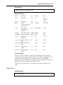
1
Device Reference Manual Device Reference Manual 2 Copyright Copyright 3 Copyright Notice Copyright ã WestDev Ltd. 2001-2015, and SiMetrix Technologies Ltd Pulsonix is a Trademark of WestDev Ltd. All rights reserved. E&OE Copyright in the whole and every part of this software and manual belongs to WestDev Ltd. and SiMetrix Technologies Ltd. and may not be used, sold, transferred, copied or reproduced in whole or in part in any manner or in any media to any person, without the prior written consent of WestDev Ltd. If you use this manual you do so at your own risk and on the understanding that neither WestDev Ltd. nor associated companies shall be liable for any loss or damage of any kind. WestDev Ltd. does not warrant that the software package will function properly in every hardware software environment. Although WestDev Ltd. has tested the software and reviewed the documentation, WestDev Ltd. makes no warranty or representation, either express or implied, with respect to this software or documentation, their quality, performance, merchantability, or fitness for a particular purpose. This software and documentation are licensed 'as is', and you the licensee, by making use thereof, are assuming the entire risk as to their quality and performance. In no event will WestDev Ltd. be liable for direct, indirect, special, incidental, or consequential damage arising out of the use or inability to use the software or documentation, even if advised of the possibility of such damages. WestDev Ltd. reserves the right to alter, modify, correct and upgrade our software programs and publications without notice and without incurring liability. Microsoft, Windows, Windows NT and Intellimouse are either registered trademarks or trademarks of Microsoft Corporation. All other trademarks are acknowledged to their respective owners. Pulsonix, a division of WestDev Ltd. Printed in the UK. Issue date: 26/06/15 iss 3 Pulsonix 20 Miller Court Severn Drive Tewkesbury Business Park Tewkesbury Glos, GL20 8DN United Kingdom Phone Fax Email Support +44 (0)1684 296 551 +44 (0)1684 296 515 [email protected] [email protected] 4 Copyright Contents 5 Contents CONTENTS ................................................................................................................................ 5 CHAPTER 1. SIMULATOR DATA FORMATS............................................................................. 9 Netlist Format ................................................................................................................................. 9 File Format................................................................................................................................. 9 Language Declaration ............................................................................................................... 10 Comments ................................................................................................................................ 10 Device Lines ............................................................................................................................ 10 Simulator Controls ................................................................................................................... 12 Simulator Output........................................................................................................................... 12 The List File ............................................................................................................................. 12 The Binary Data File ................................................................................................................ 13 Output Data Names .................................................................................................................. 13 CHAPTER 2. SIMULATOR DEVICES ........................................................................................17 Overview ...................................................................................................................................... 17 Using XSPICE Devices ................................................................................................................. 17 Vector Connections .................................................................................................................. 17 Connection Types ..................................................................................................................... 18 Using Expressions ......................................................................................................................... 19 Overview.................................................................................................................................. 19 Using Expressions for Device Parameters ................................................................................. 19 Using Expressions for Model Parameters .................................................................................. 20 Expression Syntax .................................................................................................................... 20 Optimisation............................................................................................................................. 27 CHAPTER 3. ANALOG DEVICE REFERENCE ..........................................................................29 Overview ...................................................................................................................................... 29 Arbitrary Source ............................................................................................................................ 29 Bipolar junction transistor ........................................................................................................ 33 Capacitor .................................................................................................................................. 37 Capacitor with Voltage Initial Condition ................................................................................... 38 Current Controlled Current Source ........................................................................................... 39 Current Controlled Voltage Source ........................................................................................... 41 Current Source ......................................................................................................................... 42 Diode – Level 1 and Lvel 3 ....................................................................................................... 42 Diode – Soft Recovery .............................................................................................................. 45 GaAsFET ................................................................................................................................. 47 Inductor (Ideal) ......................................................................................................................... 48 Inductor (Saturable) .................................................................................................................. 49 Inductor with Current Initial Condition ..................................................................................... 51 Insulated Gate Bipolar Transistor ............................................................................................. 52 Junction FET ............................................................................................................................ 53 Lossy Transmission line ........................................................................................................... 55 MOSFET.................................................................................................................................. 56 Resistor .................................................................................................................................... 62 S-domain Transfer Function Block............................................................................................ 64 Subcircuit instance ................................................................................................................... 69 Transmission line ..................................................................................................................... 69 6 Contents Voltage Controlled Current Source ...........................................................................................70 Voltage Controlled Switch ........................................................................................................71 Voltage controlled voltage source..............................................................................................72 Voltage Source .........................................................................................................................72 Pulse Source .............................................................................................................................73 Piece-Wise Linear Source .........................................................................................................74 PWL File Source ......................................................................................................................75 Sinusoidal Source .....................................................................................................................76 Exponential Source ...................................................................................................................77 Single Frequency FM ................................................................................................................78 Noise Source ............................................................................................................................78 Extended PWL Source ..............................................................................................................78 Mutual Inductor ........................................................................................................................80 CHAPTER 4. DIGITAL SIMULATION........................................................................................ 83 Logic States ...................................................................................................................................83 State resolution table ................................................................................................................84 Analog to Digital Interfaces ...........................................................................................................84 How A-D Bridges are Selected..................................................................................................86 Logic Families ...............................................................................................................................86 Logic Family Model Parameters. ...............................................................................................87 Logic Compatibility Tables .......................................................................................................87 Supported Logic Families .........................................................................................................89 Universal Logic Family.............................................................................................................89 Internal Tables ..........................................................................................................................89 Load Delay ...............................................................................................................................90 Digital Model Libraries .................................................................................................................91 Using Third Party Libraries ......................................................................................................91 Arbitrary Logic Block - User Defined Models ................................................................................91 Example 2 - A Simple Multiplier ..............................................................................................93 Example 3 - A ROM Lookup Table ...........................................................................................94 Example 4 - D Type Flip Flop...................................................................................................94 Device Definition - Netlist Entry & .MODEL Parameters .........................................................95 Language Definition - Overview ...............................................................................................97 Language Definition - Constants and Names .............................................................................97 Language Definition - Ports ......................................................................................................97 Language Definition - Registers and Variables ..........................................................................98 Language Definition - Assignments ......................................................................................... 102 Language Definition - User and Device Values ....................................................................... 104 Diagnostics : Trace File .......................................................................................................... 105 Mixed-mode Simulator - How it Works ....................................................................................... 105 Event Driven Digital Simulator ............................................................................................... 105 Interfacing to the Analog Simulator ......................................................................................... 106 Enhancements over XSPICE ........................................................................................................ 107 CHAPTER 5. DIGITAL DEVICE REFERENCE ........................................................................ 109 Digital Device Reference ............................................................................................................. 109 Common Parameters ............................................................................................................... 109 Delays .................................................................................................................................... 110 And Gate ................................................................................................................................ 110 D-type latch ............................................................................................................................ 111 D-type flip flop ....................................................................................................................... 113 Contents 7 Buffer ..................................................................................................................................... 115 Digital Capacitor .................................................................................................................... 117 Frequency Divider .................................................................................................................. 120 Digital Initial Condition.......................................................................................................... 121 Digital Pulse........................................................................................................................... 122 Digital Resistor ...................................................................................................................... 123 Digital Signal Source .............................................................................................................. 124 Inverter................................................................................................................................... 127 JK Flip Flop ........................................................................................................................... 128 Arbitrary Logic Block ............................................................................................................. 131 Nand Gate .............................................................................................................................. 132 Nor Gate ................................................................................................................................ 133 Open-Collector Buffer ............................................................................................................ 134 Open-Emitter Buffer ............................................................................................................... 135 Or Gate .................................................................................................................................. 137 Pulldown Resistor .................................................................................................................. 138 Pullup Resistor ....................................................................................................................... 138 Random Access Memory ........................................................................................................ 139 Set-Reset Flip-Flop................................................................................................................. 140 SR Latch ................................................................................................................................ 142 State Machine ........................................................................................................................ 144 Toggle Flip Flop ..................................................................................................................... 145 Tri-State Buffer ...................................................................................................................... 147 Exclusive NOR Gate .............................................................................................................. 148 Exclusive OR Gate ................................................................................................................. 149 Analog-Digital Converter ........................................................................................................ 150 Analog-Digital Interface Bridge .............................................................................................. 153 Digital-Analog Converter ........................................................................................................ 157 Digital-Analog Interface Bridge .............................................................................................. 159 Controlled Digital Oscillator ................................................................................................... 162 Analog-Digital Schmitt Trigger ............................................................................................... 163 INDEX...................................................................................................................................... 166 8 Contents Simulator Data Formats 9 Chapter 1. Simulator Data Formats Netlist Format The Pulsonix Spice netlist format follows the general format used for all SPICE and SPICE compatible simulators. However, with so many SPICE derivatives and with two significantly different versions of SPICE itself (SPICE 2 and SPICE 3) it is not possible to define a standard SPICE format. Pulsonix Spice has been developed to be as compatible as possible with model libraries that can be obtained from external sources. For discrete devices, models are usually SPICE 2 compatible but some use extensions originally developed for PSpice©. IC designers usually receive model files from fabrication companies and these tend to be developed for Star-Hspice©. Pulsonix Spice is compatible with all of these but simultaneous compatibility with all formats is not technically possible due to a small number of syntax details - such as the character used for in line comments. To overcome these minor difficulties, a language declaration can be placed at the top of the netlist and any file included using .INC or the Star-Hspice© variant of .LIB. This is described in the following sections. File Format A complete netlist consists of: · A title line · Optional language declaration · Device lines · Control lines · Comment lines The title line must be the first line of the file and may be empty. The remaining lines, with some exceptions, may be placed in any order All other lines are defined by their first non-whitespace character as follows. · Control lines begin with a period: '.' · Comment lines begin with an asterix: '*' · Device lines begin with a letter A line is usually terminated with a new line character but may be continued using the '+' continuation character. So if the first non-whitespace character is a '+' the line will be considered to be an extension of the previous line. SPICE requires the '+' to be the first character, Pulsonix Spice allows whitespace (space or tab) to precede it. 10 Simulator Data Formats Language Declaration Pulsonix Spice is able to read PSpice©, Star-Hspice© and native Pulsonix Spice netlists, but in some cases needs to be instructed what format netlist it is reading. Currently there are three areas where simultaneous compatibility has not been possible. These are: · Inline comment character. · Unlabelled device parameters · The meaning of LOG() and PWR() functions Pulsonix Spice can be instructed to use any of the two non-native languages by using the language declaration. This is one of: *#HSPICE *#PSPICE The language declaration must be placed at the top of the file immediately below the title line. It can also be placed in files referenced using .INC or the HSPICE© version of .LIB in which case it will apply only to that file and any others that it calls. A language declaration placed anywhere else in a file will be ignored. Comments Any line other than a language declaration beginning with a '*' is defined as a comment and will be ignored. Also anything between a semi-colon ';' ('$' in HSPICE mode) and the end of the line will be treated as comment and will also be ignored. Some SPICE simulators require the '*' character to be the first character of the line. Pulsonix Spice allows it to be preceded by white space (spaces and tabs). Device Lines Device lines usually follow the following basic form but each type of device tends to have its own nuances: Name nodelist value [parameters] value may be an actual number e.g. in the case of passive components such as resistors, or it may be a model name in the case of semiconductor devices such as bipolar transistors. Models are defined using a .MODEL control line. nodelist is a list of net names. The number and order of these is device dependent. The net name itself may consist of any collection of non-control ASCII characters except whitespace and '.'. All other ASCII characters are accepted although it is suggested that the following characters are avoided if possible: \ " % & + - * / ^ < > [ ] ' @ { } If any of these characters are used in a net name, a special syntax will be needed to plot any signal voltage on that net. This is explained in the “Output Data Names” section below. In addition the characters ‘[‘, ‘]’, ‘%’, ‘!’ and ‘~’ have a special meaning when used with XSPICE devices and therefore should be avoided at all times. Simulator Data Formats 11 The name is the circuit reference of the device. The first letter of this name determines the type of device as shown in the table below. The Pin Names column in the following table is relevant to the vector name used for values of device pin current. See the “Output Data Names” section. Letter No of pins Device A Any XSPICE devices Pin Names depends on device B 2 Arbitrary source P, N C 2 Capacitor P, N D 2 Diode P, N E 4 Voltage controlled voltage source P, N, CP, CN F 2 Current controlled current source P, N G 4 Voltage controlled current source P, N, CP, CN H 2 Current controlled voltage source P, N I 2 Fixed current source P, N J 3 JFET D, G, S K 0 Coupling for inductors - L 2 Inductor P, N M 4 MOSFET D, G, S, B N - Not used - O 4 Lossy transmission line P1, N1, P2, N2 P - Not used - Q 3-5 Bipolar transistor C, B, E, S, DT R 2 Resistor P, N S 4 Voltage controlled switch P, N, CP, CN T 4 Lossless transmission line P1, N1, P2, N2 U - Not used - V 2 Voltage source P, N W - Not used - X Any Subcircuit - Y - Not used - Z 3 GaAs FET D, G, S IGBT C, G, E To remove the naming restriction that this system imposes, Pulsonix Spice supports an extension to the above to allow the user to use any name for all devices. If the device letter is followed by a dollar '$' symbol (by default but can be changed - see below), the remainder of the name following the '$' will be used as the device name. E.g.: Q$TR23 12 Simulator Data Formats will define a bipolar transistor with the name TR23. All output generated by the simulator will refer to TR23 not Q$TR23. This mechanism will be disabled if HSPICE or PSPICE languages are specified. Simulator Controls Instructions to the simulator other than device definitions and comments are referred to as controls and always begin with a period '.'. Full documentation for the simulator controls, see the User s Guide. Simulator Output The List File Pulsonix-Spice produces a list file by default. This receives all text output except for the Monte Carlo log. This includes operating point results, model parameters, noise analysis results, sensitivity analysis results, pole-zero analysis results and tabulated vectors specified by .PRINT. The list file is generated in the same directory as the netlist. It has the same name as the netlist but with the extension .OUT. There are a number of options that control the list file output. Option name Description PARAMLOG Valid values: Full All instance and model parameter values reported Given All user specified model parameters and parameterised instance parameters Brief Parameterised model and instance parameters None None Default = Given EXPAND Flag. If specified, the netlist with all sub-circuits expanded will be output to the list file EXPANDFILE String. If specified the expand netlist will be output to the specified file rather than the list file NOMOD Same as PARAMLOG=none. Model parameters will not be output WIDTH Page width in number of characters. (The list file is formatted assuming that it will be read or printed using a fixed width font such as Courier.) The default is 80 but any value may be used not just 80 and 132 as in SPICE 2. OPINFO If set DC operating point info file is created for all analyses (except .SENS). Normally it is created only for .OP analyses Simulator Data Formats 13 The Binary Data File The simulation data is stored in a binary data file. The format is proprietary to Pulsonix and is not compatible with SPICE ‘raw’ files. The name and location of the binary file depends on configuration settings and in what mode the simulator is run. The file is usually stored in a temporary location and is named according to the analysis type and appended with the extension .sxdat. E.g.tran1.sxdat, ac2.sxdat, dc3.sxdat etc. To save this data to your own location see the Saving Data section in the Graphs & Probes chapter of the Pulsonix Spice Users Guide. Only Pulsonix-Spice can read the simulator's binary data file. When run from a schematic design, the file is automatically loaded and in fact it is not usually necessary to know anything about it except perhaps when it grows very large and fills up your disk. From the command shell you can explicitly load the data file when the run is complete. This can be done with the command shell menu File|Data|Load…. After the data is loaded, the results can be plotted in the usual manner. Output Data Names For transient, DC and AC analyses, Pulsonix-Spice calculates and stores the circuit’s node voltages and device pin currents and these are all given unique names. If using probing techniques with the Pulsonix schematic editor you don't usually need to know anything about the names used. However there are situations where it is necessary or helpful to know how these names are derived. An example is when compiling an expression relating voltages and currents to be used in a .PRINT control. Another is when plotting results created by simulating a netlist that was not generated using the schematic editor. The names used are documented in the following notes. Top Level Node Voltages The vector names used for node voltages at the top level (i.e. not in a subcircuit) are simply the name of the node used in the netlist. Subcircuit Node Voltages For nodes within a subcircuit, the name is prefixed with the subcircuit reference and a '.'. For example: X1 N1 N2 N3 SubName X2 N4 N5 N6 SubName .SUBCKT 1 2 3 SubName X3 N1 2 N3 SubName2 R1 VIN 0 1k ... .ENDS .SUBCKT 1 2 3 SubName2 V1 VCC 0 5 ... .ENDS 14 Simulator Data Formats The internal node VIN in definition SubName referenced by X1 would be called X1.VIN. The same node referenced by X2 would be called X2.VIN. The node VCC defined in subcircuit SubName2 would be named X1.X3.VCC and X2.X3.VCC for X1 and X2 respectively. Nodes with Non-standard Names A non-standard node name is one that begins with a digit or which contains one or more of the characters: \ " % & + - * / ^ < > [ ] ' @ { } These are legal but introduce problems when accessing the voltage data that they carry. The above characters can be used in arithmetic expressions so cause a conflict if used as a node name. In order to access the voltage data on a node so named, use the Vec() function: Vec('node_name') Example with .PRINT and node called V+ .PRINT TRAN {Vec('V+')} A similar syntax is required when using the front end plotting commands. Device Pin Currents Device pin currents are named in the following form: device_name#pin_name For primitive devices (i.e. not sub-circuits) pin_name must comply with the table defined in the Pulsonix-Spice Users Guide, in the Device Library and Model Management Chapter, section Simulator Device Pin Names. For example the current into the collector of Q23 would be Q23#c. The pin names for sub-circuits depend on whether the pinnames: specifier (see “Subcircuit Instance” in the Pulsonix Spice Device Reference Manual) is included in the netlist entry for the device. If it is the pin current name will be the name listed after pinnames:. If it isn't then they are numbered in sequence starting from 1. The order is the same as the order they appear in the netlist device line. For example, if the subcircuit line is: X$U10 N1 N2 N3 N4 N5 LM324 pinnames: VINP VINN VP VN VOUT The current into the last pin (connected to N5) would be U10#VOUT (Note that 'X$' is stripped off). If the netlist line is: X$U10 N1 N2 N3 N4 N5 LM324 The same current would be U10#5 Simulator Data Formats 15 Internal Node Voltages Some devices have internal nodes and the voltages on these are output by the simulator. These are named in a similar manner to pin currents i.e. device_name#internal_node_name The internal_node_name depends on the device. For example, bipolar transistors create an internal node for each terminal that specifies a corresponding resistance parameter. So if the RE parameter is specified an internal node will be created called emitter. 16 Simulator Data Formats Simulator Devices 17 Chapter 2. Simulator Devices Overview This chapter is an introduction to the “Analog Device Reference and the “Digital/Mixed Signal Device Reference”. The device reference chapters describe all simulator devices at the netlist level. The netlist consists of a list of component definitions, along with simulator commands, which the simulator can understand. Simple components, such as resistors just need a value to define them. Other more complicated devices such as transistors need a number of parameters to describe their characteristics. The device references includes details of all device and model parameters. Using the schematic editor and model library you may not often need to read this section. Some of the devices, however, have advanced options not directly supported by the user interface. For example, many devices allow a local temperature to be specified. This requires the component value to be appended with TEMP=…. This device parameter and others are documented here. Note that many parts either supplied with Pulsonix Spice or available from component manufacturers are implemented as subcircuits. These are circuit designs to simulate the behaviour of high level devices such as opamps. Pulsonix does not have an opamp device built in but use these macro models instead. Full documentation for these devices is beyond the scope of this manual but can sometimes be obtained from their suppliers. Using XSPICE Devices Some devices are implemented as part of the XSPICE ‘code modelling’ framework. This framework introduces some new features at the netlist level not supported by standard SPICE devices. These new features are described in this section. Most of the devices that use this framework are digital or mixed signal devices and the reference for these can be found at “Digital/Mixed Signal Device Reference” However there are three all analog devices that are also XSPICE devices. These are: · · · “Capacitor with Voltage Initial Condition” “Inductor with Current Initial Condition” “S-domain Transfer Function Block” Vector Connections Some models feature an arbitrary number of inputs or/and outputs. For example, an AND gate can have any number of inputs. It would be inflexible to have a separate model for every configuration of AND gate so a method of grouping connections together has been devised. These are known as vector connections. Vector connections are enclosed in square brackets. E.g. the netlist entry for an AND gate is: Axxxx [ in_0 in_1 .. in_n ] out model_name 18 Simulator Devices The pins in_0 in_1 to in_n form a single vector connection. Any number of pins may be placed inside the square brackets, in fact the same model may be used for devices with different numbers of inputs. Some devices have a minimum and/or maximum number of pins that may be used in a vector connection. This is known as vector bounds and if they apply will be listed in the vector bounds column of the Connection Details table provided with every device definition. To add vector connections to a schematic part, use the pin properties button on the Define Spice Type dialog. See the Device Library and Model Management chapter in the Pulsonix Spice User’s Manual for details on how to do this. Connection Types In the device references that follow, each has a table titled "Connection Details". Each table has the column entries "Default type" and "Allowed types". The type referred to here is the type of electrical connection e.g. voltage, current, differential or single-ended. Some devices allow some or all of their connections to be specified with a range of types. For example, the analog-digital converter described later in Device Reference under Analog-Digital Converter has a single ended voltage input by default. However, using a simple modification to the netlist entry, an ADC can be specified with a differential voltage input or even a differential current. Changing the type of connection involves no changes to the .MODEL control, only to the netlist entry. The following table lists all the available types. The modifier is the text used to alter a connection type at the netlist level. This is explained below Description Modifier Single ended voltage %v Single ended current %i Differential voltage %vd Differential current %id Digital %d Grounded conductance (voltage input current output) %g Grounded resistance (current input, voltage output) %h Differential conductance (voltage input current output) %gd Differential resistance (voltage input current output) %hd With the models supplied with Pulsonix Spice, only the first four in the above table are ever offered as options. The others are used but are always compulsory, and an understanding of their meaning is not necessary to make full use the system. As well as type, all connections also have a direction. This can be in, out or inout. Voltage, current and digital connections may be in or out while the conductance and resistance connections may only be inout. Voltage inputs are always open circuit, current inputs are always short circuit, voltage outputs always have zero output impedance and current outputs always have infinite output impedance. Simulator Devices 19 The conductance connections are a combined voltage input and current output connected in parallel. If the output is made to be proportional to the input, the connection would be a conductor with a constant of proportionality equal to its conductance, hence the name. Similarly, the resistance connections are a combined current input and voltage output connected in series. If the output is made to be proportional to the input, the connection would be a resistor with a constant of proportionality equal to its resistance. Changing Connection Type If a model allows one or more of its connections to be given a different type, this can be done by preceding the connection entry with the appropriate modifier listed in the table above. For example if you wish to specify a 4 bit ADC with a differential voltage input, the netlist entry would be something like: A1 %vd ANALOG_INP ANALOG_INN CLOCK_IN [ DATA_OUT_0 DATA_OUT_1 DATA_OUT_2 DATA_OUT_3 ] DATA_VALID ADC_4 Using Expressions Overview Expressions consist of arithmetic operators, functions, variables and constants and maybe employed in the following locations: · As device parameters · As model parameters · To define a variable which can itself be used in an expression · As the governing expression used for arbitrary sources They have a wide range of uses. For example: · To define a number of device or model parameters that depend on some common characteristic. This could be a circuit specification such as the cut-off frequency of a filter or maybe a physical characteristic to define a device model. · To define tolerances used in Monte Carlo analyses. · Used with an arbitrary source, to define a non-linear device. Using Expressions for Device Parameters Device or instance parameters are placed on the device line. For example the length parameter of a MOSFET, L, is a device parameter. A MOSFET line with constant parameters might be: M1 1 2 3 4 MOS1 L=1u W=2u L and W could be replaced by expressions. For example M1 1 2 3 4 MOS1 L={LL-2*EDGE} W={WW-2*EDGE} 20 Simulator Devices Device parameter expressions must usually be enclosed with either single quotation marks ( ' ) double quotation marks ( " ) or braces ( '{' and '}' ). The expression need not be so enclosed if it consists of a single variable. For example: .PARAM LL=2u WW=1u M1 1 2 3 4 MOS1 L=LL W=WW Using Expressions for Model Parameters The rules for using expressions for device parameters also apply to model parameters. E.g. .MODEL N1 NPN IS=is BF={beta*1.3} Expression Syntax The expression describing an arbitrary source consists of the following elements: Circuit variables · Parameters · Constants. Operators · Functions · Look up tables These are described in the following sections Circuit Variables Circuit variables may only be used in expressions used to define arbitrary sources and to define variables that themselves are accessed only in arbitrary source expressions. Circuit variables allow an expression to reference voltages and currents in any part of the circuit being simulated. Voltages are of the form: V(node_name) Where node_name is the name of the net carrying the voltage of interest. Currennts are of the form: I(source_name) Where source_name is the name of a voltage source carrying the current of interest. The source may be a fixed voltage source, a current controlled voltage source, a voltage controlled voltage source or an arbitrary voltage source. It is legal for an expression used in an arbitrary source to reference itself e.g.: Implements a 100 ohm resistor. Parameters These are defined using the .PARAM control. See Pulsonix Spice Users Guide, Command reference section for more details. For example Simulator Devices 21 .PARAM res=100 B1 n1 n2 V=res*I(B1) Also implements a 100 ohm resistor. For release 2 and later it is possible to put circuit variables in .PARAM controls. For example: .PARAM VMult = { V(a) * V(b) } B1 1 2 V = Vmult + V(c) Built-in Parameters A number of parameter names are assigned by the simulator. These are: Parameter name Description TIME Resolves to time for transient analysis. Resolves to 0 otherwise including during the pseudo transient operation point algorithm. TEMP Resolves to current circuit temperature HERTZ Resolves to frequency during AC sweep and zero in other analysis modes PTARAMP Resolves to value of ramp during pseudo transient point algorithm. operating Constants Apart from simple numeric values, arbitrary expressions may also contain the following built-in constants: Constant name Value Description PI 3.14159265358979323846 π E 2.71828182845904523536 e TRUE 1.0 FALSE 0.0 ECHARGE 1.6021918e-19 coulombs Charge on an electron in BOLTZ 1.3806226e-23 Boltzman's constant If the simulator is run from the front end in GUI mode, it is also possible to access variables defined on the Command Shell command line or in a script. The variable must be global and enclosed in braces. E.g. B1 n1 n2 V = V(n3, n3) * { global:amp_gain } amp_gain could be defined in a script using the LET command. E.g. “Let global:amp_gain = 100” 22 Simulator Devices Operators These are listed below and are listed in order of precedence. Precedence controls the order of evaluation. So 3*4 + 5*6 = (3*4) + (5*6) = 42 and 3+4*5+6 = 3 + (4*5) + 6 = 29 as '*' has higher precedence than '+'. Operator Description ~!- Digital NOT, Logical NOT, Unary minus ^ or ** Raise to power *, / Multiply, divide +, - Plus, minus >=, <=, >< Comparison operators ==, != or <> Equal, not equal & Digital AND (see below) | Digital OR (see below) && Logical AND || Logical OR Comparison, Equality and Logical Operators These are Boolean in nature either accepting or returning Boolean values or both. A Boo lean value is either TRUE or FALSE. FALSE is defined as equal to zero and TRUE is defined as not equal to zero. So, the comparison and equality operators return 1.0 if the result of the operation is true otherwise they return 0.0. The arguments to equality operators should always be expressions that can be guaranteed to have an exact value e.g. a Boolean expression or the return value from functions such as SGN. The == operator, for example, will return TRUE only if both arguments are exactly equal. So the following should never be used: v(n1)==5.0 v(n1) is never likely to be exactly 5.0. It may be 4.9999999999 or 5.00000000001 but only by fluke will it be 5.0. These operators are intended to be used with the IF() function described below. Digital Operators These are the operators '&', '|' and '~'. These were introduced in release 1.0 as a simple means of implementing digital gates in the analog domain. Their function has largely been superseded by gates in the event driven simulator but they are nevertheless still supported. Although they are used in a digital manner the functions implemented by these operators are continuous in nature. They are defined as follows: Simulator Devices 23 Expression Condition Result out = x & y x<vtl OR y<vtl out = vl out = x|y x>vth AND y>vth out = vh x>vth AND vth>y>vtl out = (y-vtl)*(vh-vl)/(vth-vtl)+vl vtl<x< vth AND y>vth out = (x-vtl)*(vh-vl)/(vth-vtl)+vl vtl<x< vth AND vth>y>vtl out = (y-vtl)*(x-vtl)*(vh-vl)/(vthvtl) 2+vl x<vtl AND y<vtl out = vl x>vth OR y>vth out = vh x<vtl AND vth>y>vtl out = vh-(vth-y)*(vh-vl)/(vth-vtl) vtl<x< vth AND y<vtl vtl<x< vth AND vth>y>vtl out = vh-(vth-x)*(vh-vl)/(vth-vtl) out = vh-(vth-y)*(vth-x)*(vh-vl)/(vthvtl out = ~x x<vtl out = vh x>vth out = vl vtl<x<vth out = (vth-x)/(vth-vtl)*(vh-vl)+vl Where: vth = upper input threshold vtl = lower input threshold vh = output high vl = output low These values default to 2.2, 2.1, 5 and 0 respectively. These values are typical for high speed CMOS logic (74HC family). They can be changed with four simulator options set by the .OPTIONS simulator control. These are respectively, LOGICTHRESHHIGH, LOGICTHRESHLOW, LOGICHIGH, LOGICLOW To change the lower input threshold to 1.9, add the following line to the netlist: .OPTIONS LOGICTHRESHLOW=1.9 To find out how to add additional lines to the netlist when using the schematic editor, refer to “Adding Extra Netlist Lines” in the Pulsonix-Spice Users Guide. Functions Function Description ABS(x) Magnitude of x. if x>=0 result=x otherwise result=-x ACOS(x) Arc cosine. Result is in radians ACOSH(x) Inverse COSH 24 Simulator Devices ASIN(x) Arc sine. Result is in radians ASINH(x) Inverse SINH ATAN(x) Arc tangent. Result is in radians ATAN2(x,y) =ATAN(x/y). Valid if y=0. Result in radians ATANH(x) Inverse TANH COS(x) Cosine of x in radians COSH(x) Hyperbolic cosine DDT(x) Differential of x with respect to time EXP(x) ex FLOOR(x) Next lowest integer of x. IF(cond, x, y) if cond is TRUE result=x else result=y IFF(cond, x, y) As IF(cond, x, y) LIMIT(x, lo, hi) if x<lo result=lo else if x>hi result=hi else result=x LN(x) Log to base e of x. If x<10-100 result=-230.2585093 LOG(x) Log to base 10 of x. If x<10-100 result=-100 LOG10(x) Log to base 10 of x. If x<10-100 result=-100 MAX(x, y) Returns larger of x and y MIN(x,y) Returns smaller of x and y PWR(x,y) |x|y PWRS(x,y) if x>=0 |x|y else -|x|y SDT(x) Integral of x with respect to time SGN(X) If x>0 result = 1 else if x<0 result = -1 else result = 0 SIN(x) Sine of x in radians SINH(x) Hyperbolic sine SQRT(x) if x>=0 vx else v-x STP(x) If x<=0 result = 0 else result = TAN(x) Tangent of x in radians TANH(x) Hyperbolic tangent U(x) as STP(x) URAMP(x) if x<0 result =0 else result = x Simulator Devices 25 Monte Carlo Distribution Functions To specify Monte Carlo tolerance for a model parameter, use an expression containing one of the following 12 functions: Name Distribution Lot? GAUSS Gaussian No GAUSSL Gaussian Yes UNIF Uniform No UNIFL Uniform Yes WC Worst case No WCL Worst case Yes GAUSSE Gaussian logarithmic No GAUSSEL Gaussian logarithmic Yes UNIFE Uniform logarithmic No UNIFEL Uniform logarithmic Yes WCE Worst case logarithmic No WCEL Worst case logarithmic Yes A full discussion on the use of Monte Carlo distribution functions is given in the Pulsonix-Spice Users Guide. Look-up Tables Expressions may contain any number of look-up tables. This allows a transfer function of a device to be specified according to - say - measured values without having to obtain a mathematical equation. Look-up tables are specified in terms of x, y value pairs which describe a piece-wise linear transfer function. Look up tables are of the form: TABLE[ xy_pairs ]( input_expression ) Where: xy_pairs such A sequence of comma separated pairs of constant values that define the input and output values of the table. For each pair, the first value is the x or input value and the second is the y or output value. Only explicit numberic constants may be used. Even internal constants as PI may not be used. input_expression Expression defining the input or x values of the table. Example The following arbitrary source definition implements a soft limiting function 26 Simulator Devices B1 n2 n3 v=table[-10, -5, -5, -4, -4, -3.5, -3, -3, 3, 3, 4, 3.5, 5, 4, 10, 5] (v(N1)) and has the following transfer function: It is possible to assign expressions to component values which are evaluated when the circuit is simulated. This has a number of uses. For example you might have a filter design for which several component values affect the roll off frequency. Rather than recalculate and change each component every time you wish to change the roll of frequency it is possible to enter the formula for the component’s value in terms of this frequency. The above circuit is that of a two pole low-pass filter. C1 is fixed and R1=R2. The design equations are: R1=R2=2/(2*pi*f0*C1*alpha) C2=C1*alpha*alpha/4 where f0 is the cut off frequency and alpha is the damping factor. The complete netlist for the above circuit is: V1 V1_P 0 AC 1 0 Simulator Devices 27 C2 0 R1_P {C1*alpha*alpha/4} C1 VOUT R1_N {C1} E1 VOUT 0 R1_P 0 1 R1 R1_P R1_N {2/(2*pi*f0*C1*alpha)} R2 R1_N V1_P {2/(2*pi*f0*C1*alpha)} Before running the above circuit you must assign values to the variables. This can be done by one of three methods: · With the .PARAM control placed in the netlist. · With Let command from the command line or from a script. (If using a script you must prefix the parameter names with global:) · By sweeping the value with using parameter mode of a swept analysis · or multi-step analysis Expressions for device values must be entered enclosed in curly braces ('{' and '}'). Suppose we wish a 1kHz roll off for the above filter. Using the .PARAM control, add these lines to the netlist .PARAM f0 1k .PARAM alpha 1 .PARAM C1 10n For more information on .PARAM Using the Let command, you would type: Let f0=1k Let alpha=1 Let C1=10n If you then wanted to alter the damping factor to 0.8 you only need to type in its new value: Let alpha=0.8 then re-run the simulator. To execute the Let commands from within a script, prefix the parameter names with global:. E.g. “Let global:f0=1k” In many cases the .PARAM approach is more convenient as the values can be stored with the schematic. Optimisation Overview An optimisation algorithm may be enabled for expressions used to define arbitrary sources and any expression containing a swept parameter. This can improve performance if a large number of such expressions are present in a design. 28 Simulator Devices The optimiser dramatically improves the simulation performance of the power device models developed by Infineon. See “Optimiser Performance” below. Why is it Needed? The simulator’s core algorithms use the Newton-Raphson iteration method to solve nonlinear equations. This method requires the differential of each equation to be calculated and for arbitrary sources, this differentiation is performed symbolically. So as well calculating the user supplied expression, the simulator must also evaluate the expression’s differential with respect to each dependent variable. These differential expressions nearly always have some sub-expressions in common with subexpressions in the main equation and other differentials. Calculation speed can be improved by arranging to evaluate these sub-expressions only once. This is the main task performed by the optimiser. However, it also eliminates factors found on both the numerator and denominator of an expression as well as collecting constants together wherever possible. Using the Optimiser The optimiser will automatically be enabled for any arbitrary source or swept expression that uses a function defined using .FUNC. To enable for all expressions, use the following option setting: .OPTIONS optimise=2 Conversely, optimisation can be disable completely with: Optimiser Performance The optimisation algorithm was added to Pulsonix Spice primarily to improve the performance of some publicly available power device models from Infineon. These models make extensive use of arbitrary sources and many expressions are defined using .FUNC. The performance improvement gained for these model is in some cases dramatic. For example a simple switching PSU circuit using a SGP02N60 IGBT ran around 5 times faster with the optimiser enabled and there are other devices that show an even bigger improvement. Accuracy The optimiser simply changes the efficiency of evaluation and doesn’t change the calculation being performed in any way. However, performing a calculation in a different order can alter the least significant digits in the final result. In some simulations, these tiny changes can result in much larger changes in circuit solution. So, you may find that switching the optimiser on and off may change the results slightly. Analog Device Reference 29 Chapter 3. Analog Device Reference Overview This section provides the full details of every option and parameter available with every primitive SPICE device that the simulator supports. This also includes details of device model parameters. Using the schematic editor and model library you will not often need to read this section. Some of the devices, however, have advanced options not directly supported by the user interface. For example, many devices allow a local temperature to be specified. This requires the component value to be appended with "TEMP=...". This device parameter and others are documented here. Note that many parts either supplied with Pulsonix Spice or available from component manufacturers are implemented as subcircuits. These are circuit designs to simulate the behaviour of high level devices such as opamps. Pulsonix Spice (and all other SPICE simulators) do not have an opamp device built in but use these macro models instead. Full documentation for these devices is beyond the scope of this manual but can sometimes be obtained from their suppliers. Arbitrary Source Schematic Entry Parts: “Arbitrary Current Source” and “Arbitrary Voltage Source” Netlist Entry Voltage source: Bxxxx n+ n- [MIN=min_value] [MAX=max_value] V=expression Current source: Bxxxx n+ n- [MIN=min_value] [MAX=max_value] i=expression Charge source: Bxxxx n+ n- Q=expression Flux source: Bxxxx n+ n- FLUX=expression 30 Analog Device Reference An arbitrary source is a voltage or current source whose output can be expressed as an arbitrary relationship to other circuit voltages or currents. expression Algebraic expression describing voltage or current output in terms of circuit nodes or sources. See Expression syntax in “Using Expressions” for more details. min_value Minimum value of source max_value Maximum value of source bxxxx Component reference n+ Positive output node n- Negative output node The small-signal AC behaviour of the non-linear source is a linear dependent source with a proportionality constant equal to the derivative (or derivatives) of the source at the DC operating point. Note that if MIN and/or MAX parameters are specified, they must precede the defining expression. Charge and Flux sources implement capacitors and inductors respectively. See “Charge and Flux devices” below. If the source is a current, the direction of flow is into the positive node (n+). Notes on Arbitrary Expression It is generally beneficial if the expression used for an arbitrary source is well conditioned. This means that it is valid for all values of its input variables (i.e. circuit voltages and currents) and that it is continuous. It is also desirable - although rarely absolutely necessary - for the function to be continuous in its first derivative; i.e. it does not have any abrupt changes in slope. If the expression is used in a feedback loop then these conditions are more or less essential for reliable and rapid convergence. If the arbitrary source is used open loop then these conditions can be relaxed especially if the input signal is well defined e.g. derived directly from a signal source. Some functions are not continuous in nature. E.g. the STP() and SGN() functions are not. These may nevertheless be used in an expression as long as the end result is continuous. Similarly, the IF() function should be used with care. The following IF() function is continuous: IF(v1>v2, 0, (v1-v2)*2) When v1=v2 both true and false values equate to zero so the function has no abrupt change. The function still has a discontinuous first derivative with respect to both v1 and v2 which is still undesirable but will work satisfactorily in most situations. The following example is not continuous: Analog Device Reference 31 IF(v1>v2, 0, 5) The result of this will switch abruptly from 0 to 5 when v1=v2. This is not something that the simulator can be guaranteed to handle and cannot be implemented in real life. A better, albeit less intuitive method, of achieving the intent of the above is: (TANH((v2-v1)*factor)+1)*2.5+2.5 where factor is some number that determines the abruptness of the switching action. For a value of 147, 95% of the full output will be achieved with just 10mV overdrive. Charge and Flux Devices From version 2 it is possible to define capacitors and inductors directly using the arbitrary source. Capacitors must be defined in terms of their charge and inductors by their flux. These are defined in the same as voltage and current arbitrary sources but using ‘q’ or ‘flux’ instead of ‘v’ or ‘i’. E.g. the following defines a simple linear capacitor: B1 n1 n2 Q = C*V(n1,n2) Similarly a linear inductor is: B1 n1 n2 flux = L * i(B1) The main benefit of this feature is that it makes it possible to define non-linear capacitors and inductors directly. Previously, this was only possible by making up a circuit consisting of a number of components including a primitive capacitor. As with voltage and current arbitrary sources, it is possible to use any combination of voltages and currents in the expression. So, for example, the following defines a transformer: Bprimary p1 p2 flux = Lp*i(Bprimary) + M*i(Bsecondary) Bsecondary s1 s2 flux = Ls*i(Bsecondary) + M*i(Bprimary) Arbitrary Source Examples Example 1 - Voltage Multiplier The expression for an arbitrary source must refer to other voltages and/or currents on the schematic. Currents are referenced as voltage sources and voltages as netnames. Netnames are usually allocated by the schematic editor. For information on how to display and edit the schematic's netnames, refer to the Pulsonix Schematic documentation. R4 n1 10k 1K R1 B1 V=V=V(n2)*V(n1) n2 1K R3 1K R2 32 Analog Device Reference In the above circuit the voltage across B1 will be equal to the product of the voltages at nodes n1 and n2. An alternative approach is to define the arbitrary source within a subcircuit. E.g. .subckt MULT out in1 in2 B1 out 0 V=V(in1)*V(in2) .ends which can be added to the netlist manually. (To find out how to add additional lines to the netlist when using the schematic editor, refer to "Adding Extra Netlist Lines" in the Pulsonix-Spice Users Guide). A symbol could be defined for it and then placed on the schematic as a block as shown below: R4 1K X1 R1 1K MULT R2 1K R3 1K Example 2 - Voltage comparator B3 q3_b 0 V=atan(V(n1,n2)*1000) This can also be added to the schematic in the same way as for the multiplier described above. Example 3 - Ideal Power Converter This examples also demonstrates the use of expressions within subcircuits. (See Using Expressions) The following subcircuit implements an idealised power converter with an efficiency of eff and whose output voltage is proportional to the input voltage (vinn,vinp) multiplied by the control voltage (vcp,vcn). It is intended to simulate the voltage/current characteristics of a switching power converter. .subckt powerconv voutp voutn vinp vinn vcp vcn biin1 vinp vinn i=-v(voutp,voutn)/v(vinp,vinn)*i(vout1)/{eff} vout1 bmult1_n voutn 0 bmult1 voutp bmult1_n v=v(vinp,vinn)*v(vcp,vcn) r1 vcp vcn 1meg .ends Once again, with an appropriate schematic symbol, the device can be placed on the schematic as a block as shown below: Analog Device Reference 33 U1 D1 ideal R5 1Meg C1 270u 1000 powerconv : eff=0.7 V1 pulse( 100 0 0 1m) R1 1K E1 V2 12 3 Input NAND gate .subckt NAND_3_HC 2 3 4 1 B1 0 1 i = ~(v(2) & v(3) & v(4)) Rdel 1 0 1 Cdel 1 0 12n .ends Note this implements the gate as a current source as this is handled more efficiently by the simulator. PSPICEÒ and Star-Hspice syntax Pulsonix Spice supports the PSPICEÒ and HSPICEÒsyntax for arbitrary sources for devices defined within a subcircuit. This is for compatibility with some manufacturers device models. Both "VALUE =" and "TABLE =" devices are supported and for HSPICEÒ VOL=and CUR=are supported. Bipolar junction transistor Schematic Entry Parts: “npn” and “pnp” Netlist Entry Qxxxx collector base emitter [substrate] modelname [area] [OFF] [IC=vbe,vce] [TEMP=local_temp] 34 Analog Device Reference collector Collector node name base Base node name emitter Emitter node name substrate Substrate node name modelname Name of model, must begin with a letter but can contain any character except whitespace and ' . ' . Models with names OFF, IC, TEMP, TOL, LOT or MATCH should not be used for four terminal devices. (This restriction is a consequence of the optional substrate node.) area Area multiplying factor. Area scales up the device. E.g. an area of 3 would make the device behave like 3 transistors in parallel. Default is 1. OFF Instructs simulator to calculate operating point analysis with device initially off. This is used in latching circuits such as thyristors and bistables to induce a particular state. See section on .op. Bias Point Analysis for more details. vbe,vce Initial conditions for base-emitter and collector-emitter junctions respectively. These only have an effect if the UIC parameter is specified on the .tran control. local_temp Local temperature. Overrides specification in .options or .temp controls. BJT Examples Single BC547: 25 MJ15024’s connected in parallel with junction temperature = 85 C: NPN BJT Model Syntax .model modelname NPN ( parameters ) PNP BJT Model Syntax .model modelname PNP ( parameters ) Analog Device Reference 35 BJT Model Parameters The symbols ' ´ ' and ' ¸ ' in the Area column means that that parameter should be multiplied or divided by the area factor respectively. Name Description Units Default Area IS Transport saturation current A 1e-16 x BF Ideal maximum forward beta 100 NF Forward current emission coefficient VAF Forward Early voltage V ∞ 1.0 IKF Corner for forward beta high current rolloff A ∞ x ISE B-E leakage saturation current A 0 x NE B-E leakage emission coefficient 1.5 BR Ideal maximum reverse beta 1 NR Reverse current emission coefficient 1 VAR Reverse Early voltage V ∞ IKR Corner for reverse beta high current roll-off A ∞ x ISC B-C leakage saturation current A 0 x NC B-C leakage emission coefficient RB Zero bias base resistance Ω 0 ÷ IRB Current at which base resistance falls halfway to its minimum value A ∞ x RBM Minimum base resistance at high currents Ω RB ÷ RE Emitter resistance Ω 0 ÷ RC Collector resistance Ω 0 ÷ CJE B-E zero-bias depletion capacitance F 0 x VJE B-E built in potential V 0.75 MJE B-E junction exponential factor TF Ideal forward transit time XTF Coefficient for bias dependence of TF VTF Voltage describing VBC dependence of TF V ∞ ITF High-current parameter for effect on TF A 0 PTF Excess phase at freq=1.0/(TF2Hz degree 0 CJC B-C zero-bias depletion capacitance F 0 V 2 0.33 Sec. 0 0 VJC B-C built-in potential MJC B-C junction exponential factor 0.33 0.75 XCJC Fraction of B-C depletion capacitance connected to internal base node 1 x x 36 Analog Device Reference TR Ideal reverse transit time Sec. 0 CJS Zero-bias collector substrate capacitance F 0 VJS Substrate junction built-in potential V 0.75 MJS Substrate junction exponential factor 0 XTB Forward and reverse beta temperature exponent 0 EG Energy gap XTI Temperature exponent for effect on IS eV 3 KF Flicker noise coefficient 0 AF Flicker noise exponent 1 FC Coefficient for forward-bias depletion capacitance formula 0.5 x 1.11 Notes The bipolar junction transistor model in SPICE is an adaptation of the integral charge control model of Gummel and Poon. This modified Gummel-Poon model extends the original model to include several effects at high bias levels. The model will automatically simplify to the simpler Ebers-Moll model when certain parameters are not specified. The dc model is defined by the parameters IS, BF, NF, ISE, IKF, and NE which determine the forward current gain characteristics, IS, BR, NR, ISC, IKR, and NC which determine the reverse current gain characteristics, and VAF and VAR which determine the output conductance for forward and reverse regions. Three ohmic resistances RB, RC, and RE are included, where RB can be high current dependent. Base charge storage is modelled by forward and reverse transit times, TF and TR, the forward transit time TF being bias dependent if desired, and non-linear depletion layer capacitances which are determined by CJE, VJE, and MJE for the B-E junction , CJC, VJC, and MJC for the BC junction and CJS, VJS, and MJS for the C-S (Collector-Substrate) junction. The temperature dependence of the saturation current, IS, is determined by the energy-gap, EG, and the saturation current temperature exponent, XTI. Additionally base current temperature dependence is modelled by the beta temperature exponent XTB in the new model. This implementation includes further enhancements to model quasi-saturation effects. This is governed by the model parameters RCO, QCO, GAMMA and for temperature dependence, QUASIMOD, VG, D and CN. The quasi-saturation model is compatible with PSpice. Hspice models may be accommodated by setting RC to zero and RCO to the value of RC in the Hspice model. References The Quasi-saturation model was developed from the following paper: George M. Kull, Laurence W. Nagel, Shiuh-Wuu Lee, Peter Lloyd, E. James Prendergast and Heinz Dirks, “A Unified Circuit Model fo Bipolar Transistors Including QuasiSaturation Effects”, . IEEE Transactions on Electron Devices, Vol. ED-32, No 6 June 1985, pages 1103-1113. Analog Device Reference 37 Capacitor Schematic Entry Part: “Capacitor” Netlist Entry Cxxxx n1 n2 [model_name] value [IC=initial_condition] [TEMP=local_temp] [TC1=tc1] [TC2=tc2] [VC1=vc1] [VC2=vc2] [BRANCH=0|1] [M=mult] [DTEMP=dtemp] n1 Node1 n2 Node2 model_name (Optional) Name of model . Must begin with a letter but can contain any character except whitespace and period '.' value Capacitance (Farads) initial_condition Initial voltage if UIC specified on .tran control local_temp Capacitor temperature (°C) tc1 First order temperature coefficient tc2 Second order temperature coefficient vc1 First order voltage coefficient vc2 Second order voltage coefficient BRANCH May be 0 or 1. 0 is the default. This parameter determines the internal formulation of the capacitor and affects how the IC parameter is implemented. When BRANCH=0, the capacitor looks like an open circuit during the DC operating point and the IC parameter has no effect unless UIC is specified for a transient analysis. If BRANCH=1, the capacitor looks like a voltage source during dc operating point with a magnitude equal to the value of the IC parameter. BRANCH=1 makes it possible to specify circuit startup conditions. See Alternative Initial Condition Implementations later in this chapter for an example. mult Device multiplier. Equivalent to putting mult devices in parallel. dtemp Differential temperature. Similar to local_temp but is specified relative to circuit temperature. If both TEMP and DTEMP are specified, TEMP takes precedence. 38 Analog Device Reference Capacitor Model Syntax .model modelname CAP ( parameters ) Capacitor Model Parameters Name Description Units C Capacitor multiplier Default 1 TC1 First order temperature coefficient Second order temperature coefficient 1/°C 1/°C2 0 TC2 First order voltage coefficient Volt-1 0 Second order voltage coefficient Volt-2 0 VC1 VC2 0 Capacitor with Voltage Initial Condition Schematic Entry: Part: “Capacitor (XSPICE)” Netlist entry: Axxxx cap_p cap_n model_name Connection details: Name Description cap Direction Default type Allowed types Vector bounds Capacitor terminals inout hd hd n/a Model format: .MODEL model_name cm_cap parameters Model parameters: Name Description Type Default Limits c Capacitance real ic Voltage initial condition real Vector? Vector bounds none 1E-21 - INF No n/a 0 none n/a No Description This is like a standard capacitor but the internal implementation is different and permits the specification of an initial condition which works without having to specify the transient UIC switch. Also, unlike normal initial conditions, the initial voltage is applied with a zero source resistance. In some circumstances, large value capacitors are better implemented using this device than the standard capacitor but note that during the DC operating point solution, the Analog Device Reference 39 device looks like a short circuit, not an open circuit as is the case with the normal SPICE device. Current Controlled Current Source Schematic Entry Part: “Current Controlled Current Src” Netlist Entry: Linear Source Fxxxx nout+ nout- vc current_gain nout+ Positive output node nout- Negative output node vc Controlling voltage source current_gain Output current/Input current SPICE2 polynomial sources are also supported in order to maintain compatibility with commercially available libraries for IC's. (Most operational amplifier models for example use several polynomial sources). In general, however the arbitrary source is more flexible and easier to use. Netlist Entry: Polynomial Source Fxxxx nout+ nout- POLY( num_inputs ) vc1 vc2 ... polynomial_specification vc1, vc2 Controlling voltage sources num_inputs Number of controlling currents for source. polynomial_specification See below The specification of the controlling voltage source or source requires additional netlist lines. The schematic netlister automatically generates these for the four terminal device supplied in the symbol library. 40 Analog Device Reference Example R2 1K 0.1 F1 R1 1K In the above circuit, the current in the output of F1 (flowing from top to bottom) will be 0.1 times the current in R2. Polynomial Specification The following is an extract from the SPICE2G.6 user manual explaining polynomial sources. SPICE allows circuits to contain dependent sources characterised by any of the four equations i=f(v) v=f(v) i=f(i) v=f(i) where the functions must be polynomials, and the arguments may be multidimensional. The polynomial functions are specified by a set of coefficients p0, p1, ..., pn. Both the number of dimensions and the number of coefficients are arbitrary. The meaning of the coefficients depends upon the dimension of the polynomial, as shown in the following examples: Suppose that the function is one-dimensional (that is, a function of one argument). Then the function value fv is determined by the following expression in fa (the function argument): fv = p0 + (p1.fa) + (p2.fa2) + (p3.fa3) + (p4.fa4) + (p5.fa5) + ... Suppose now that the function is two-dimensional, with arguments fa and fb. Then the function value fv is determined by the following expression: fv = p0 + (p1.fa) + (p2.fb) + (p3.fa2) + (p4.fa.fb) + (p5.fb2) + (p6.fa3) + (p7.fa2.fb) + (p8.fa.fb2) + (p9.fb3) + ... Consider now the case of a three-dimensional polynomial function with arguments fa, fb, and fc. Then the function value fv is determined by the following expression: fv = p0 + (p1.fa) + (p2.fb) + (p3.fc) + (p4.fa2) + (p5.fa.fb) + (p6.fa.fc) + (p7.fb2) + (p8.fb.fc) + (p9.fc2) + (p10.fa3) + (p11.fa2.fb) + (p12.fa2.fc) + (p13.fa.fb2) + (p14.fa.fb.fc) + (p15.fa.fc2) + (p16.fb3) + (p17.fb2.fc) + (p18.fb.fc2) + (p19.fc3) + (p20.fa4) + ... Analog Device Reference 41 Note: If the polynomial is one-dimensional and exactly one coefficient is specified, then SPICE assumes it to be p1 (and p0 = 0.0), in order to facilitate the input of linear controlled sources. Current Controlled Voltage Source Schematic Entry Part: “Current Controlled Voltage Src” Netlist Entry : Linear Source Hxxxx nout+ nout- vc transresistance nout+ Positive output node nout- Negative output node vc Controlling voltage source transresistance Output current/Input current (W) SPICE2 polynomial sources are also supported in order to maintain compatibility with commercially available libraries for IC's. (Most Op-amp models use several polynomial sources). In general, however the arbitrary source is more flexible and easier to use. Netlist Entry : Polynomial Source Hxxxx nout+ nout- POLY( num_inputs ) vc1 vc2 ... polynomial_specification vc1, vc2 Controlling voltage sources num_inputs Number of controlling currents for source. polynomial_specification See previous section on polynomial specification The specification of the controlling voltage source or source requires additional netlist lines. The schematic netlister automatically generates these for the four terminal device supplied in the symbol library. 42 Analog Device Reference Current Source Schematic Entry Parts: “Fixed Current Source” , “Current Pulse Generator” and “Current Sine Generator” Netlist Entry Ixxxx n+ n- [DC dcvalue] [AC magnitude [phase]] [transient_spec] n+ Positive node n- Negative node dcvalue Value of source for dc operating point analysis magnitude AC magnitude for AC sweep analysis. Phase phase for AC sweep analysis transient_spec Specification for time varying source. Can be one of following: Pulse – see Pulse Source section later Piece wise linear - see Piece wise linear Source section later Sine - see Siusoidale Source section later Exponential - see Exponential Source section later Single frequency FM - see Single frequency FM section later Diode – Level 1 and Lvel 3 Schematic Entry Part: “Diode” Netlist Entry Dxxxx n+ n- model_name [area] [OFF] [IC=vd] [TEMP=local_temp] + [M=mult] [PJ=periphery] [L=length] [W=width] [DTEMP=dtemp] n+ Anode n- Cathode model_name Name of model defined in a .model control. Must begin with a letter but can contain any character except whitespace and ' . ' . area Area multiplying factor. Area scales up the device. E.g. an area of 3 would make the device behave like 3 diodes in parallel. Default is 1. Analog Device Reference 43 OFF Instructs simulator to calculate operating point analysis with device initially off. This is used in latching circuits such as thyristors and bistables to induce a particular state. See .op. Bias Point Analysis for more details. vd Initial condition for diode voltage. This only has an effect if the UIC parameter is specified on the .tran control local_temp Local temperature. Overrides specification in .options or .temp controls. mult Level 3 only. Similar to area. See below. periphery Level 3 only. Junction periphery used for calculating sidewall effects. length Level 3 only. Used to calculate area. See below. width Level 3 only. Used to calculate area. See below. mult Device multiplier. Equivalent to putting mult devices in parallel. dtemp Differential temperature. Similar to local_temp but is specified relative to circuit temperature. If both TEMP and DTEMP are specified, TEMP takes precedence. Examples D1 D1N4148 D2 5 BYT12 D3 D1N914 TEMP=100 Diode Model Syntax .model modelname D (LEVEL=[1|3] parameters ) Diode Model Parameters – Level = 1 The symbols ' × ' and ' ÷ ' in the Area column means that that parameter should be multiplied or divided by the area factor respectively. Diode Model Parameters The symbols ' ´ ' and ' ¸ ' in the Area column means that that parameter should be multiplied or divided by the area factor respectively. Name Description Units Default Area IS Transport saturation current A 1e-14 ´ ISR Recombination current parameter A 0 ´ N Emission coefficient 1 NR Emission Coefficient for ISR 2 44 Analog Device Reference IKF High injection knee current A ¥ ´ RS Series resistance W 0 ¸ TT Transit time sec 0 CJO or CJ0 Zero bias junction capacitance F 0 VJ Junction potential V 1 M Grading coefficient EG Energy gap XTI Saturation current temperature exponent 3 KF Flicker noise coefficient 0 AF Flicker noise exponent 1 FC Forward bias depletion capacitance coefficient 0.5 BV Reverse breakdown voltage V ¥ IBV Current at breakdown voltage A 1e-10 TNOM Parameter measurement temperature °C 27 TRS1 First order tempco RS /°C ´ 0.5 eV 1.11 2 TRS2 Second order tempco RS /°C TBV1 First order tempco BV /°C TBV2 Second order tempco BV /°C2 ´ 0 0 Notes: The dc characteristics of the diode are determined by the parameters IS, N, ISR, NR and IKF. An ohmic resistance, RS, is included. Charge storage effects are modelled by a transit time, TT, and a non-linear depletion layer capacitance which is determined by the parameters CJO, VJ, and M. The temperature dependence of the saturation current is defined by the parameters EG, the energy and XTI, the saturation current temperature exponent. Reverse breakdown is modelled by an exponential increase in the reverse diode current and is determined by the parameters BV and IBV (both of which are positive numbers). Diode Model Parameters - Level = 3 Name AF BV CJO, CJ CJSW CTA CTP EG FC FCS GAP1 Description Flicker noise exponent Reverse breakdown voltage Zero bias junction capacitance Zero bias sidewall capacitance CJO temp coefficient. (TLEVC=1) CJSW temp coefficient. (TLEVC=1) Energy gap Forward bias depletion capacitance coefficient Forward bias sidewall capacitance coefficient 7.02e-4 - silicon (old value) 4.73e-4 - silicon 4.56e-4 - germanium Units V F F °C-1 °C-1 ev 0.5 eV/° Default 1.0 ∞ 0.0 0.0 1.11 0.5 7.02e-4 Analog Device Reference 45 5.41e-4 - gallium arsenide 1108 - silicon (old value) 636 - silicon 210 - germanium 204 - gallium arsenide Current at breakdown voltage High injection knee current Reverse high injection knee current Saturation current Recombination current Sidewall saturation current Flicker noise exponent Grading coefficient Sidewall grading coefficient Forward emission coefficient Recombination emission coefficient Sidewall built in potential Series resistance Shrink factor GAP2 IBV IKF, IK IKR IS, JS ISR JSW KF MJ, M MJSW N, NF NR PHP RS SHRINK ° 1108 A A A A A A 1E-3 • • 1E-14 0 0 0 0.5 0.33 1.0 2.0 PB Ω TCV BV temp coefficient °C-1 TLEV TLEVC TNOM, TREF TPB TPHP TRS TT VJ, PB XW Temperature model selector. Valid values 0,1,2 Temperature model selector. Valid values 0,1,2 Parameter measurement temperature VJ temp coefficient (TLEVC=1) PHP temp. coefficient (TLEVC=1) RS temp. coefficient Transit time Built-in potential Shrink factor 0 0 V/°C V/°C °C-1 S V 0 1.0 0 27 0.0 0.0 0.0 0.0 0.8 0.0 The parameters CJSW and JSW are scaled by the instance parameter PJ whose default value is 0.0. If L and W instance parameters are supplied, the diode is scaled by the factor: M*(L*SHRINK-XW)*(W*SHRINK-XW) otherwise it is scaled by M*AREA. M and AREA are instance parameters which default to 1.0 Diode – Soft Recovery Netlist Entry Dxxxx n+ n- model_name [TEMP=local_temp] n+ Anode n- Cathode model_name Name of model defined in a .MODEL control. Must begin with a letter but can contain any character except whitespace and '. ' . local_temp Local temperature. Overrides specification in .OPTIONS or .TEMP controls. 46 Analog Device Reference Diode Model Syntax .model modelname SRDIO ( parameters ) Soft Recovery Diode Model Parameters Name Description Units Default CJO Zero bias junction capacitance F 0.0 EG Energy gap ev 1.11 FC Forward bias depletion capacitance coefficient IS Saturation current MJ Grading coefficient 0.5 N Forward emission coefficient 1.0 RS Series resistance TNOM Parameter measurement temperature TT Diffusion transit time TAU Minority carrier lifetime VJ Built-in potential XTI Saturation current temperature exponent 0.5 A Ω 1E-15 0 27 S 5e-6 1e-5 V 1 3 Basic Equations The model is based on the paper “A Simple Diode Model with Reverse Recovery” by Peter Lauritzen and Cliff Ma. (See references). The model’s governing equations are quite simple and are as follows: In addition the model uses the standard SPICE equations for junction capacitance and temperature dependence of IS. References Peter O. Lauritzen, Cliff L. Ma, A Simple Diode Model with Reverse Recovery, IEEE Transactions on Power Electronics, Vol. 6, No 2, pp 188-191, April 1991. Analog Device Reference 47 GaAsFET Netlist Entry Zxxxx drain gate source modelname [area] [OFF] [IC=vds , vgs] drain Drain node gate Gate node source Source node modelname Name of model defined in a .model control. Must begin with a letter but can contain any character except whitespace and period '.' . area Area multiplying factor. Area scales up the device. E.g. an area of 3 would make the device behave like 3 transistors in parallel. Default is one. OFF Instructs simulator to calculate operating point analysis with device initially off. This is used in latching circuits such as thyristors and bistables to induce a particular state. See .op Control. Bias Point Analysis for more details. vds,vgs Initial conditions for drain-source and gate-source junctions respectively. These only have an effect if the UIC parameter is specified on the .tran control. GaAsFET Model Syntax .model modelname NMF ( parameters ) GaAsFET Model Parameters The symbols ' ´ ' and ' ¸ ' in the Area column means that parameter should be multiplied or divided by the area factor respectively. Name Description Units Default VTO Pinch-off Voltage V -2.0 Transconductance parameter A/V2 2.5e-3 BETA Area ´ B Doping tail extending parameter 1/V 0.3 ALPHA Saturation voltage parameter 1/V 2 LAMBDA Channel length modulation parameter 1/V 0 RD Drain ohmic resistance Ω 0 ¸ RS Source ohmic resistance Ω 0 ¸ CGS Zero bias gate source capacitance F 0 ´ CGD Zero bias gate drain capacitance F 0 ´ 48 Analog Device Reference PB Gate junction potential V 1 IS Gate p-n saturation current A 1e-14 FC Forward bias depletion capacitance coefficient KF Flicker noise coefficient 0 AF Flicker noise exponent 1 ´ 0.5 Notes: The GaAsFET model is derived from the model developed by Statz. The DC characteristics are defined by parameters VTO, B and BETA, which determine the variation of drain current with gate voltage, ALPHA, which determines saturation voltage, and LAMBDA, which determines the output conductance. IS determines the gate-source and gate-drain dc characteristics. Two ohmic resistances are included. Charge storage is modelled by total gate charge as a function of gate-drain and gate-source voltages and is defined by the parameters CGS, CGD and PB. Inductor (Ideal) Schematic Entry Part: “Saturable Transformer” Netlist Entry Lxxxx n1 n2 value [IC=init_cond] [BRANCH=0|1] n1 Node 1 n2 Node 2 value Value in henries init_cond Initial current in inductor. Only effective if UIC option is specified on .tran control. BRANCH set to 0 or 1. 1 is default value. This parameter determines the internal formulation of the inductor and affects how the IC parameter is implemented. When BRANCH=1, the inductor looks like a short circuit during DC operating point and the IC parameter has no effect unless UIC is specified for a transient analysis. If BRANCH=0, the inductor looks like a source during dc operating point with a magnitude equal to the value of the IC parameter. BRANCH=0 makes it possible to specify circuit startup conditions. Analog Device Reference 49 See Also Mutual Inductance later in this chapter Non-linear Inductors later in this chapter Inductor (Saturable) Schematic Entry Part: “Ideal Inductor” Netlist Entry Lxxxx n1 n2 modelname [IC=init_cond] [N=num_turns] [LE=le] [AE=ae] [UE=ue] n1 Node 1 n2 Node 2 modelname Model name referring to a .MODEL control describing the core characteristics. See details below. num_turns Number of turns on winding le Effective path length of core in metres. Default = PATH/100. PATH is defined in .MODEL. ae Effective area of core in metres2. Default = AREA/10000 where AREA is define in .MODEL. ue Effective permeability of core. Overrides model parameter of the same name. Model format - Jiles-Atherton model with hysteresis .MODEL model_name CORE parameters Model format - simple model without hysteresis .MODEL model_name CORENH parameters Jiles-Atherton Parameters Name PATH C K MS GAP GAPM A AREA UE AHMODE Description Effective path length Domain flexing parameter Domain anisotropy parameter Magnetisation saturation Air gap (centimetres) Air gap (metres) Thermal energy parameter amp.mEffective area Effective permeability. Overrides GAP and GAPM if >0. See notes Anhysteric function selector (see notes) Units cm 0.2 amp.m-1 1E6 cm m 1000 cm2 Default 1 500 0 GAP/100 0.1 0 50 Analog Device Reference Non-hysteresis Model Parameters Name PATH MS GAP GAPM A AREA AHMODE Description Effective path length Magnetisation saturation Air gap (centimetres) Air gap (metres) Thermal energy parameter amp.mEffective area Anhysteric function selector (see notes) Units cm cm m 1000 cm2 Default 1 1E6 0 GAP/100 0.1 0 Notes on the Jiles-Atherton model The Jiles-Atherton model is based on the theory developed by D.C. Jiles and D.L.Atherton in their 1986 paper “Theory of Ferromagnetic Hysteresis”. The model has been modified to correct non-physical behaviour observed at the loop tips whereby the slope of the B-H curve reverses. This leads to non-convergence in the simulator. The modification made is that proposed by Lederer et al. (See refs below). Full details of the Pulsonix Spice implementation of this model including all the equations are provided in a technical note. This is located on the install CD at Docs/Magnetics/Jiles-AthertonModel.pdf. The AHMODE parameter selects the equation used for the anhysteric function, that is the non-linear curve describing the saturating behaviour. When set to 0 the function is the same as that used by PSpice. When set to 1 the function is the original equation proposed by Jiles and Atherton. See the Jiles-Atherton-Model.pdf technical note for details. If the UE parameters is specified either on the device line or in the model, an air gap value is calculated and the parameters GAP and GAPM are ignored. See the JilesAtherton-odel.pdf technical note for the formula used. The parameter names and their default values for the Jiles-Atherton model are compatible with PSpice, but the netlist entry is different. Notes on the non-hysteresis model This is simply a reduced version of the Jiles-Atherton model with the hysteresis effects removed. The anhysteric function and the air-gap model are the same as the JilesAtherton model. Implementing Transformers This model describes only a 2 terminal inductor. A transformer can be created using a combination of controlled sources along with a single inductor. The Pulsonix schematic editor uses this method. The schematic editor provides a means of creating transformers and this uses an arrangement of controlled sources to fabricate a non-inductive transformer. Any inductor can be added to this arrangement to create an inductive transformer. The method is simple and efficient. The following shows how a non-inductive three winding transformer can be created from simple controlled sources: F1 0 n1 E1 1 E1 W1A W1B n1 0 1 F2 0 n1 E2 1 Analog Device Reference 51 E2 W2A W2B n1 0 1 F3 0 n1 E3 1 E3 W3A W3B n1 0 1 Connecting an inductor between n1 and 0 in the above provides the inductive behaviour. This is in fact how the Pulsonix Spice schematic editor creates non-linear transformers. Note that you cannot use the mutual inductor device with the saturable inductor. Plotting B-H curves Both models can be enabled to output values for flux density in Tesla and magnetizing force in A.m-1. To do this, add the following line to the netlist: .KEEP Lxxx#B Lxxx#H Replace Lxxx with the reference for the inductor. (e.g. L23 etc). You will find vectors with the names Lxxx#B Lxxx#H available for plotting in the waveform viewer. References 1. Theory of Ferrmagnetic Hysteresis, DC.Jiles, D.L. Atherton, Journal of Magnetism and Magnetic Materials, 1986 p48-60. 2. On the Parameter Identification and Application of the Jiles-Atherthon Hysteresis Model for Numerical Modelling of Measured Characteristics, D Lederer, H Igarashi, A Kost and T Honma, IEEE Transactions on Magnetics, Vol. 35, No. 3, May 1999 Inductor with Current Initial Condition Schematic Entry: Part: “Inductor (XSPICE)” Netlist entry: Axxxx ind_p ind_n model_name Connection details: Name Description Direction Default Allowed type types Vector bounds ind Inductor terminals inout gd n/a Model format: .MODEL model_name cm_ind parameters gd 52 Analog Device Reference Model parameters: Name Description Type Default Limits Vector? Vector bounds l Inductance real none 1e-18 INF No n/a ic Current initial condition real 0 none No n/a Description This is like a standard inductor but the internal implementation is different and permits the specification of a current initial condition which works without having to specify the transient UIC switch. In some circumstances, large value inductors are better implemented using this device than the standard inductor but note that during the DC operating point solution, the device looks like an open circuit, not a short circuit as is the case with the normal SPICE device. Note that this type of inductor cannot be coupled using the 'K' device. Insulated Gate Bipolar Transistor Schematic Entry Part: “N-Channel JFET” and “P_Channel JFET” Netlist Entry Zxxxx collector gate emitter[AREA=area] [OFF] [ARG=agd] [KP=kp] [TAU=tau] [WB=wb] Collector Collector node gate Gate node Emitter Emitter node area Device area in m2 (overrides model parameter of the same name) agd Gate-drain overlap area in m2 (overrides model parameter of the same name) kp Transconductance (overrides model parameter of the same name) tau Ambipolar recombination lifetime (overrides model parameter of the same name) wb Base width in metres (overrides model parameter of the same name) Model syntax .MODEL model_name NIGBT parameters Analog Device Reference 53 Name AGD AREA BVF BVN CGS COXD JSNE KF KP MUN MUP NB TAU THETA VT VTD WB Description Units Default Gate-drain overlap area m2 5E-6 Device active area m2 1E-5 Breakdown voltage nonplanar junction factor 1.0 Avalanche multiplication exponent 4.0 Gate-source capacitance per unit area Fcm-2 1.24E-8 Gate-drain overlap oxide capacitance per unit area Fcm-2 3.5E-8 Emitter electron saturation current density Acm-2 6.5E-13 Triode region MOSFET transconductance factor 1.0 MOSFET transconductance factor AV-2 0.38 Electron mobility cm-2(Vs)-1 1.5E3 Hole mobility cm-2(Vs)-1 4.5E2 Base doping concentration cm-3 2E14 Ambipolar recombination lifetime s 7.1E-6 Transverse field transconductance factor V-1 0.02 MOSFET channel threshold voltage V 4.7 Gate-drain overlap depletion threshold V 1E-3 Metallurgical base width m 9.0E-5 Notes The IGBT model is based on the model developed by Allen R. Hefner at the National Institute of Standards and Technology. The parameter names, default values and units have been chosen to be compatible with the PSpice implementation of the same model. For more information, please refer to: Modelling Buffer Layer IGBT’s for Circuit Simulation, Allen R. Hefner Jr, IEEE Transactions on Power Electronics, Vol. 10, No. 2, March 1995 An Experimentally Verified IGBT Model Implemented in the Saber Circuit Simulator, Allen R. Hefner, Jr., Daniel M. Diebolt, IEE Transactions on Power Electronics, Vol. 9, No. 5, September 1994 Junction FET Schematic Entry Part: “N-Channel JFET” and “P_Channel JFET” Netlist Entry Jxxxx drain gate source modelname [area] [OFF] [IC=vds,vgs] [TEMP=local_temp] drain Drain node gate Gate node source Source node modelname Name of model defined in a .model control. Must begin with a letter but can contain any character except whitespace and period '.' . 54 Analog Device Reference area Area multiplying factor. Area scales up the device. E.g. an area of 3 would make the device behave like 3 transistors in parallel. Default is 1. OFF Instructs simulator to calculate operating point analysis with device initially off. This is used in latching circuits such as thyristors and bistables to induce a particular state. See op. Bias Point Analysis for more details. vds,vgs Initial conditions for drain-source and gate-source junctions respectively. These only have an effect if the UIC parameter is specified on the .tran control. local_temp Local temperature. Overrides specification in .options or .temp controls. N Channel JFET: Model Syntax .model modelname NJF ( parameters ) P Channel JFET: Model Syntax .model modelname PJF ( parameters ) JFET: Model Parameters The symbols ' ´ ' and ' ¸ ' in the Area column means that parameter should be multiplied or divided by the area factor respectively. Name Description Units Default VTO Threshold voltage Transconductance parameter V A/V2 -2.0 BETA BETATCE BETA temperature coefficient % 0 LAMDA Channel length modulation parameter 1/V 0 RD Drain ohmic resistance W 0 ¸ RS Source ohmic resistance W 0 ¸ CGS Zero-bias G-S junction capacitance F 0 ¸ CGD Zero-bias G-D junction capacitance F 0 ¸ M Grading coefficient PB Gate junction potential V 1 IS Gate junction saturation current A 1e-14 N Gate junction emission coefficient 1 XTI IS temperature coefficient 3 KF Flicker noise coefficient 0 AF Flicker noise exponent 1 1e-4 Area ´ 1.0 ´ Analog Device Reference 55 FC Coefficient for forward bias depletion capacitance TNOM Parameter measurement temperature 0.5 °C 27 Examples BF244 U430 Temp=100 Q1 Q2 Q2 is a U430 with a local temperature of 100°C. Lossy Transmission line Schematic Entry Part: “Transmission Line (Lossy)” Netlist Entry Oxxxx p1 n1 p2 n2 modelname [IC=v1,i1,v2,i2] p1 Positive input port 1 n1 Negative input port 2 p2 Positive input port 1 n2 Negative input port 2 modelname Name of model defined in a .model control. Must begin with a letter but can contain any character except whitespace and period '.' . v1,i1,v2,i2 Initial conditions for voltage at port 1, current at port 1, voltage at port 2 and current at port 2 respectively. These only have an effect if the UIC parameter is specified on the .tran control. Lossy Transmission Line: Model Syntax .model modelname LTRA ( parameters ) Lossy Transmission Line: Model Parameters Name Description Units Default R Resistance/unit length W/unit length 0.0 L Inductance/unit length Henrys/unit length 0.0 G Conductance/unit length Siemens(mhos)/unit length 0.0 56 Analog Device Reference C Capacitance/unit length Farads/unit length 0.0 LEN Length Required These remaining parameters control the way the line is simulated rather than its electrical characteristics. More accurate results ( at the expense of simulation time) can be obtained by using lower values. REL Relative rate of change of derivative for breakpoint 1.0 ABS Absolute rate of change of derivative for breakpoint 1.0 Notes: The uniform RLC/RC/LC/RG transmission line model (LTRA) models a uniform constant-parameter distributed transmission line. The LC case may also be modelled using the lossless transmission line model. The operation of the lossy transmission line model is based on the convolution of the transmission line's impulse responses with its inputs. The following types of lines have been implemented: RLC Transmission line with series loss only RC Uniform RC line LC Lossless line RG Distributed series resistance and parallel conductance All other combinations will lead to an error. REL and ABS are model parameters that control the setting of breakpoints. A breakpoint is a point in time when an analysis is unconditionally performed. The more there are the more accurate the result but the longer it will take to arrive. Reducing REL and/or ABS will yield greater precision. Example T1 RG58_10m The above could represent a 10 metre length of RG58 cable. The parameters would be described in a .model control e.g. .model RG58_10m LTRA( R=0.1 C=100p L=250n LEN=10) MOSFET Schematic Entry Part: “Nmos – 4 term IC” and “Pmos – 4 term IC” Analog Device Reference 57 Netlist Entry Mxxxx drain gate source bulk modelname [L=length] [W=width] + [AD=drain_area] [AS=source_area] + [PD=drain_perimeter] [PS=source_perimeter] + [NRD=drain_squares] [NRS=source_squares] [NRB=bulk_squares] + [OFF] [IC=vds,vgs,vbs] [TEMP=local_temp] [M=area] drain Drain node gate Gate node source Source node bulk Bulk (substrate) node Definitions modelname Name of model. Must begin with a letter but can contain any character except whitespace and period '.' (The following 8 parameters are not supported by the level 7 MOSFET model) length Channel length (metres). width Channel width (metres). drain_area Drain area (m2). source_area Source area (m2). drain_perimeter Drain perimeter (metres). source_perimeter Source perimeter (metres). drain_squares Equivalent number of squares for drain diffusion. source_squares Equivalent number of squares for source diffusion. gate_squares Equivalent number of squares for gate resistance, Level 3 only. bulk_squares Equivalent number of squares for gate resistance, Level 3 only. OFF Instructs simulator to calculate operating point analysis with device initially off. This is used in latching circuits such as thyristors and bistables to induce a particular state. Se.op Control. Bias Point Analysis for more details. vds, vgs, vbs Initial condition voltages for drain-source gate-source and bulk(=substrate)-source respectively. These only have an effect if the UIC parameter is specified on the .tran control. local_temp Local temperature. Overrides specification in .options or .temp controls. Notes: Pulsonix Spice supports four types of MOSFET model specified in the model definition. These are referred to as levels 1, 2, 3 and 7. Levels 1,2, and 3 are the same as 58 Analog Device Reference the SPICE2 and SPICE3 equivalents. Level 7 is proprietary to Pulsonix Spice. For further information see Level 7 MOSFET parameters below. NMOS Model Syntax .model modelname NMOS ( level= 1|2|3|7 parameters ) PMOS Model Syntax .model modelname PMOS ( level= 1|2|3|7 parameters ) MOS Levels 1, 2 and 3 : Model Parameters Name Description Units Default Levels VTO or VT0 Threshold voltage V 0.0 all KP Transconductance parameter A/V2 2.0e-5 all GAMMA Bulk threshold parameter ÖV 0.0 all PHI Surface potential V 0.6 all LAMBDA Channel length modulation 1/V 0.0 all RG Gate ohmic resistance W 0.0 1&3 RD Drain ohmic resistance W 0.0 all RS Source ohmic resistance W 0.0 all RB Bulk Ohmic resistance W 0.0 3 CBD B-D junction capacitance F 0.0 all CBS B-S junction capacitance F 0.0 all IS Bulk junction sat. current A 1.0e-14 all PB Bulk junction potential V 0.8 all CGSO Gate-source overlap capacitance F/m 0.0 all CGDO Gate-drain overlap capacitance F/m 0.0 all CGBO Gate-bulk overlap capacitance F/m 0.0 all RSH Drain and source diffusion resistance W/square 0.0 all CJ Zero bias bulk junction bottom capacitance/sqmetre of junc. area F/m2 0.0 all Analog Device Reference 59 MJ Bulk junction bottom grading coefficient CJSW Zero bias bulk junction sidewall capacitance MJSW Bulk junction sidewall grading coefficient JS Bulk junction saturation current/sq-metre of junction area JSSW Bulk p-n saturation sidewall current/length TT Bulk p-n transit time 0.5 all 0.0 all 0.5 (level1) 0.33 (level 2 ,3 ) all A/m2 0.0 all A/m 0.0 3 0.0 3 1e-7 all 0.0 all 0.0 all 0.0 2,3 F/m TOX Oxide thickness NSUB Substrate doping NSS Surface state density metre 1/cm3 1/cm2 NFS Fast surface state density 1/cm2 TPG Type of gate material: all +1 opposite. to substrate -1 same as substrate 0 Al gate XJ Metallurgical junction depth metre 0.0 2,3 LD Lateral diffusion 0.0 all UO Surface mobility metre cm2/Vs 600 all UCRIT Critical field for mobility V/cm 0.0 2 UEXP Critical field exponent in mobility degradation 0.0 2 UTRA Transverse field coeff (mobility) 0.0 1,3 VMAX Maximum drift velocity of carriers 0.0 2,3 NEFF Total channel charge (fixed and mobile) coefficient 1.0 2 FC Forward bias depletion capacitance coefficient 0.5 all TNOM, T_MEASU RED Parameter measurement temperature °C 27 all T_ABS Model operating temperature °C .TEMP all m/s 60 Analog Device Reference T_REL_GL OBAL Temperature relative to current temperature KF Flicker noise coefficient °C 0 all 0.0 all AF Flicker noise exponent 1.0 all DELTA Width effect on threshold voltage 0.0 2,3 THETA Mobility modulation 0.0 3 ETA Static feedback 1/V 0.0 3 KAPPA Saturation field factor 0.2 3 W Width metre DEFW 1,2,3 (see notes) L Length metre DEFL 1,2,3 (see notes) CJ Default If not specified CJ defaults to √(εs*q* NSUB* 1e6 /(2*PB)) where εs = 1.03594314e-10 (permittivity of silicon) q = 1.6021918e-19 (electronic charge) NSUB, PB model parameters Notes for levels 1, 2 and 3: The three levels 1 to 3 are as follows: LEVEL 1. Shichman-Hodges model. The simplest and is similar to the JFET model. LEVEL 2 A complex model which models the device according to an understanding of the device physics. LEVEL 3 Simpler than level 2. Uses a semi-empirical approach i.e. the device equations are partly based on observed effects rather than the theory governing its operation. The L and W parameters perform the same function as the L and W parameters on the device line. If omitted altogether they are set to the option values (set with .options control) DEFL and DEFW respectively. These values in turn default to 100 microns. The above models differ from all other Pulsonix Spice (and SPICE) models in that they contain many geometry relative parameters. The geometry of the device (length, width etc.) is entered on a per component basis and various electrical characteristics are calculated from parameters which are scaled according to those dimensions. This is approach is very much geared towards integrated circuit simulation and is inconvenient for discrete devices. If you are modelling a particular device by hand we recommend you use the level 7 model which is designed for discrete vertical devices. Analog Device Reference 61 MOS Level 7 : Model Parameters Name Description Units Default VTO or VT0 Threshold voltage V 0.0 KP 2 Transconductance parameter A/V 2.0e-5 GAMMA Bulk threshold parameter ÖV 0.0 PHI Surface potential V 0.6 LAMBDA Channel length modulation 1/V 0.0 RD Drain ohmic resistance W 0.0 RS Source ohmic resistance W 0.0 CBD B-D junction capacitance F 0.0 CBS B-S junction capacitance F 0.0 IS Bulk junction sat. current A 1.0e-14 PB Bulk junction potential V 0.8 CGSO Gate-source overlap capacitance F 0.0 CGBO Gate-bulk overlap capacitance F 0.0 CJ Zero bias bulk junction bottom capacitance F 0.0 MJ Bulk junction bottom grading coefficient CJSW Zero bias bulk junction sidewall capacitance MJSW Bulk junction sidewall grading coefficient 0.5 FC Forward bias depletion capacitance coefficient 0.5 TNOM Parameter measurement temperature KF Flicker noise coefficient 0.0 AF Flicker noise exponent 1.0 CGDMAX Max value of gate-drain capacitance F 0.0 CGDMIN Min value of gate-drain capacitance F 0.0 XG1CGD cgd max-min crossover gradient XG2CGD cgd max-min crossover gradient VTCGD cgd max-min crossover threshold voltage V TC1RD First order temperature coefficient of rd 1/°C TC2RD Second order temperature coefficient of rd 0.5 F 0.0 °C 27 1.0 1.0 0.0 2 1/°C 0.0 0.0 Notes for level 7: The level 7 MOSFET was developed to model discrete vertical MOS transistors rather than the integrated lateral devices that levels 1 to 3 are aimed at. Level 7 is based on level 1 but has the following important additions and changes: · 5 new parameters to model gate-drain capacitance 62 Analog Device Reference · 2 new parameters to model rdson variation with temperature. · All parameters are absolute rather than geometry relative. (e.g. capacitance is specified in farads not farads/meter) All MOSFET models supplied with Pulsonix Spice are level 7 types. Many models supplied by manufacturers are subcircuits made up from a level 1, 2 or 3 device with additional circuitry to correctly model the gate-drain capacitance. While the latter approach can be reasonably accurate it tends to be slow because of its complexity. Gate-drain capacitance equation: Cgd = ( 0. 5 - p1 .tan -1 (( VTCGD - v ). - XG1CGD)).CGDMIN +( 0. 5 - p1 .tan -1 (( VTCGD - v ). XG2CGD)).CGDMAX where v is the gate-drain voltage. This is an empirical formula devised to fit measured characteristics. Despite this it has been found to follow actual measured capacitance to remarkable accuracy. To model gate-drain capacitance quickly and to acceptable accuracy set the five Cgd parameters as follows: 1. Set CGDMIN to minimum possible value of Cgd i.e. when device is off and drain voltage at maximum. 2. Set CGDMAX to maximum value of Cgd i.e. when device is on with drainsource voltage low and gate-source voltage high. If this value is not known use twice the value of Cgd for Vgd=0. 3. Set XG2CGD to 0.5, XG1CGD to 0.1 and leave VTCGD at default of 0. Although the parasitic reverse diode is modelled, it is connected inside the terminal resistances, RD and RS which does not represent real devices very well. Further, parameters such as transit time (TT) which model the reverse recovery characteristics of the parasitic diode are not included. For this reason it is recommended that the reverse diode is modelled as an external component. Models supplied with Pulsonix Spice are subcircuits which include this external diode. Resistor Schematic Entry Part: “Resistor (Box Shape)” and “Resistor (Z shape)” Netlist Entry Rxxxx n1 n2 [model_name] [value] [L=length] [W=width] [ACRES=ac_resistence] [TEMP=local_temp] [TC1=tc1] [TC2=tc2] [M=mult] [DTEMP=dtemp] n1 Node 1 n2 Node 2 Analog Device Reference 63 Definitions model_name (Optional) Name of model, see Using Model Library. Must begin with a letter but can contain any character except whitespace and '.' value Resistance (W) length Length of resistive element in metres. Only used if value is omitted. See notes below width Width of resistive element in metres. Only used if value is omitted. See notes below ac_resistance Resistance used for AC analyses and for the calculation of thermal noise. If omitted, value defaults to final resistance value. local_temp Resistor temperature (°C) tc1 First order temperature coefficient tc2 Second order temperature coefficient Mult Device multiplier. Equivalent to putting mult devices in parallel. dtemp Differential temperature. Similar to local_temp but is specified relative to circuit temperature. If both TEMP and DTEMP are specified, TEMP takes precedence. If model_name is omitted, value must be specified. • If model_name is present and value is omitted, length and width must be specified in which case the value of the resistance is RES * RSH * L/W where RSH is the sheet resistance model parameter and RES is the resistance multiplier. See model parameters below. If ACRES is specified and non-zero its value will be used unconditionally for AC analyses and the calculation of thermal noise. Resistor Model Syntax .model modelname R ( parameters ) Resistor Model Parameters Name RES TC1 TC2 RSH KF EF Description Resistance multiplier First order temperature coefficient Second order temperature coefficient Sheet resistance Flicker noise coefficient Flicker noise exponent Units 1/°C 1/°C2 Ω/sq m2/Ω2 Default 1 0 0 0 0 1 Notes The flicker noise parameters are proprietary to Pulsonix Spice. Flicker noise voltage is: Vn2 = KF * RSH2/(L*W) * Vr 2 * Δf/fEF Where: Vr = Voltage across resistor. 64 Analog Device Reference The equasion has been formulated so that KF is constant for a given resitive material. If one of L, W is not specified, the flicker noise voltage becomes: Vn = KF * R2 * Vr * Δf/fEF 2 2 Where R is the final resistance. i.e. the noise current is independent of resistance. This doesn't have any particular basis in physical laws and is implemented this way simply for convenience. When resistor dimensions and resistivity are unavailable, the value of KF will need to be extracted for each individual value. S-domain Transfer Function Block Netlist entry: Axxxx t in out model_name Connection details: Name Description Direction Default type Allowed types Vector bounds in Input in v v, vd, i, id n/a out Output out v v, vd, i, id n/a Model format: .MODEL model_name s_xfer parameters Model parameters: Name Description Type Default Limits Vector? Vector bounds in_offset Input offset real 0 none No n/a gain Gain real 1 none No n/a laplace Laplace expression (overrides num_coeff and den_coeff) string none none No n/a num_coeff Numerator poly coeff. real none Yes 1 - INF none den_coeff Denominator poly coeff. real none none Yes 1 - INF int_ic Int stage init. cond real 0 none Yes none denormalize Frequency (radians/second) real d_freq at which to denormalize coefficients Description 1 none No n/a This device implements an arbitrary linear transfer function expressed in the frequency domain using the 'S' variable. The operation and specification of the device is illustrated with the following examples. Analog Device Reference 65 Example 1 - A single pole filter 1/(s+1) LAP1 LAP1-OUTP V1 AC 1 0 1K R1 Model for above device: .model Laplace s_xfer laplace="1/(s+1)" denormalized_freq=1 1 400m 200m 100m 40m 20m 10m 20m 40m 100m 200m 400m 1 2 4 10 Frequency / Hertz Frequency response This is a simple first order roll off with a 1 second time constant. Example 2 - Single pole and zero .model Laplace s_xfer + laplace="(1/s)/(1/s + 1/(0.1*s+1))" + denormalized_freq=1 The laplace expression has been entered how it might have been written down without any attempt to simplify it. The above actually simplifies to (0.1*s+1)/(1.1*s+1) 66 Analog Device Reference 1 500m 200m 100m 10m 20m 40m 100m 200m 400m 1 2 4 10 Frequency / Hertz Example 3 - Underdamped second order response .model Laplace s_xfer + laplace="1/(s2+1.1*s+1)" + denormalized_freq=2k The above expression is a second order response that is slightly underdamped. The following graph shows the transient response. 1 0.8 0.6 0.4 0.2 0 0 Time/mSecs 2 4 6 8 10 2mSecs/div Analog Device Reference 67 Example 4 - 5th order Chebyshev low-pass filter The S-domain transfer block has a number of built in functions to implement standard filter response. Here is an example. This is a 5th order chebyshev with -3dB at 100Hz and 0.5dB passband ripple. .model Laplace s_xfer + laplace="chebyshevLP(5,100,0.5)" + denormalized_freq=1 and the response: 1 100m 10m 1m 100µ 10µ 1µ1 2 4 10 20 40 100 200 400 1k Frequency / Hertz The Laplace Expression As seen in the above examples, the transfer function of the device is defined by the model parameter LAPLACE. This is a text string and must be enclosed in double quotation marks. This may be any arithmetic expression containing the following elements: Operators: + - * / ^ ^ means raise to power. Only integral powers may be specified. Constants Any decimal number following normal rules. SPICE style engineering suffixes are accepted. S Variable This can be raised to a power with '^' or by simply placing a constant directly after it (with no spaces). E.g. s^2 is the same as s2. Filter response functions These are: 68 Analog Device Reference BesselLP( order, cut-off) Bessel low-pass BesselHP( order, cut-off) Bessel high-pass ButterworthLP( order, cut-off) Butterworth low-pass ButterworthHP( order, cut-off) Butterworth high-pass ChebyshevLP( order, cut-off, passband_ripple) Chebyshev low-pass ChebyshevHP( order, cut-off, passband_ripple) Chebyshev high-pass Where: order Integer specifying order of filter. There is no maximum limit but in practice orders larger than about 50 tend to give accuracy problems. cut-off -3dB Frequency in Hertz passband_ripple Chebyshev only. Passband ripple spec in dB Other Model Parameters · DENORMALISED_FREQ is a frequency scaling factor. · INT_IC specifies the initial conditions for the device. This is an array of maximum size equal to the order of the denominator. The right-most value is the zeroth order initial condition. · NUM_COEFF and DEN_COEFF are largely redundant but included for compatibility with other XSPICE products. They allow the literal definition of the numerator and denominator coefficients as an array. · GAIN and IN_OFFSET are the DC gain and input offset respectively Limitations Pulsonix Spice expands the expression you enter to create a quotient of two polynomials. If the constant terms of both numerator and denominator are both zero, both are divided by S. That process is repeated until one or both of the polynomials has a non-zero constant term. The result of this process must satisfy the following: · The order the denominator must be greater than or equal to that of the numerator. · The constant term of the denominator may not be zero. The XSPICE S_XFER model The Pulsonix Spice Laplace transfer model is compatible with the original XSPICE version but the transient analysis portion of it has been completely rewritten. The original XSPICE version was seriously flawed and would only give accurate results if the timestep was forced to be very small. Further, convergence would fail if the device was used inside a feedback loop. Analog Device Reference 69 Subcircuit instance Schematic Entry Some sample Parts: “HC73”, “LS73”, “Nmos – 3 term discrete”, “Opamp” Netlist Entry Xxxxx n1 n2 n3 ... subcircuit_name [pinnames: pin1 pin2 pin3 ...] [[params]: [M=m] expression1 expression2 ....] n1, n2 etc. Subcircuit nodes pin1, pin2 etc. If the "pinnames:" keyword is included the names following it will be used to name subcircuit current vectors generated by the simulator. subcircuit_name Subcircuit name referred to in subcircuit definition (i.e. with .subckt control. m Multiplier. If present, the subcircuit will be multiplied by m as if there were m devices in parallel. m may be an expression in which case it must be enclosed by curly braces: ‘{‘, ‘}’. Note that the multiplication is performed by scaling the internal devices not by actually replicating the subcircuit. Non integral values of m are thus permitted. Some types of device can not currently be scaled and subcircuits containing them will not support M. An error will displayed in this case. M will be interpreted as a regular parameter and will not scale the subcircuit instance if M is declared as a parameter in the .SUBCKT line or the following option setting is included in the netlist: .OPTIONS DisableSubcktMultiplier expression1 etc. Parameter expressions. See Using Expression.. Transmission line Schematic Entry Part: “Transmission Line (Lossless)” Netlist Entry Txxxx p1 n1 p2 n2 Z0=impedance [TD=delay] [F=frequency [NL=norm_length]] [rel=rel] [abs=abs] p1 Positive input port 1 n1 Negative input port 2 70 Analog Device Reference p2 Positive input port 1 n2 Negative input port 2 impedance characteristic impedance delay Line delay (Seconds) frequency Alternative means of specifying delay=norm_length/frequency norm_length See frequency. Default 0.25 if omitted. TD takes precedence over NL/F. Either TD or F must be specified. These remaining parameters control the way the line is simulated rather than its electrical characteristics. More accurate results ( at the expense of simulation time) can be obtained by using lower values. rel Relative rate of change of derivative for breakpoint abs Absolute rate of change of derivative for breakpoint Example T1 Z0=50 TD=1u The above line has an impedance of 50W and a delay of 1mS. Voltage Controlled Current Source Schematic Entry Part: “Voltage Controlled Current Src” Netlist Entry Gxxxx nout+ nout- vc+ vc- transconductance nout+ Positive output node nout- Negative output node vc+ Positive control node vc- Negative control node transconductance Output current/Input voltage (Siemens or mhos) SPICE2 polynomial sources are also supported in order to maintain compatibility with commercially available libraries for IC's. (Most operational amplifier models for example use several polynomial sources). In general, however the arbitrary source is more flexible and easier to use. The netlist format for a polynomial source is: Analog Device Reference 71 Gxxxx nout+ nout- POLY( num_inputs ) vc1+ vc1- vc2+ vc2- ... polynomial_specification vc1+ etc. Controlling nodes num_inputs Number of controlling node pairs for source. polynomial_specification See later in this section. Voltage Controlled Switch Schematic Entry Part: “Voltage Controlled Switch” Netlist Entry Sxxxx nout1 nout2 vc+ vc- modelname nout1 Switch node 1 nout2 Switch node 2 vc+ Positive control node vc- Negative control node modelname Name of model. Must begin with a letter but can contain any character except whitespace and period '.' . Voltage Controlled Switch Model Syntax .model modelname VSWITCH ( parameters ) OR .model modelname SW ( parameters ) Voltage Controlled Switch Model Parameters Name Description Units Default RON On resistance W 1 ROFF Off resistance W 1/GMIN VON Voltage at which switch begins to turn on V 1 VOFF Voltage at which switch begins to turn off V 0 Voltage Controlled Switch Notes The voltage controlled switch is a type of voltage controlled resistor. Between VON and VOFF the resistance varies gradually following a cubic law. 72 Analog Device Reference GMIN is a simulation parameter which defaults to 10-12 but which can changed using the .option control. The Pulsonix Spice voltage controlled switch is compatible with PSpice. but is incompatible with the standard SPICE 3 version. The latter has an abrupt switching action which can give convergence problems with some circuits. Voltage controlled voltage source Schematic Entry Part: “Voltage Controlled Voltage Src” Netlist Entry Exxxx nout+ nout- vc+ vc- gain nout+ Positive output node nout- Negative output node vc+ Positive control node vc- Negative control node gain Output voltage/Input voltage SPICE2 polynomial sources are also supported in order to maintain compatibility with commercially available libraries for IC's. (Most Op-amp models for example use several polynomial sources). In general, however the arbitrary source is more flexible and easier to use. The netlist format for a polynomial source is: Exxxx nout+ nout- POLY( num_inputs ) vc1+ vc1- vc2+ vc2- ... polynomial_specification vc1+ etc. Controlling nodes num_inputs Number of controlling node pairs for source. polynomial_specification See later in this section. Voltage Source Schematic Entry Part: “Fixed Voltage Source” Netlist Entry Vxxxx n+ n- [[DC] dcvalue] [DCOP] [INFCAP] [AC magnitude [phase]] [transient_spec] Analog Device Reference 73 N+ Positive node N- Negative node DCOP If this is specified, the voltage source will only be active during the DC operating point solution. In other analyses, it will behave like an open circuit. This is an effective method of creating a ‘hard’ initial condition. See “Alternative Initial Condition Implementations” in the Users Guidfe for an example. INFCAP If specified, the voltage source will behave as an infinite capacitor. During the DC operating point solution it will behave like an open circuit. In the subsequent analysis, it will behave like a voltage source with a value equal to the solution found during the operating point. Note that the device is inactive for DC sweeps - as all capacitors are. dcvalue Value of source for dc operating point analysis magnitude AC magnitude for AC sweep analysis. phase phase for AC sweep analysis transient_spec Specification for time varying source as described in the following table. Type Syntax Pulse pulse( v1 v2 [tdelay [trise [tfall [pulse_width [period ]]]]] ) Piece wise linear pwl ( t1 v1 [t2 v2 [t3 v3 [... ]]] ) Piece wise linear file pwlfile filename Sine sin[e] ( voffset vamplitude [frequency [delay [theta ]]] ) Exponential exp ( v1 v2 [td1 [tau1 [td2 [tau2 ]]]] ) Single frequency FM sffm ( vo va [fc [mdi [fs ]]] ) Noise noise ( interval rms_value ) Pulse Source Schematic Entry Parts: “Waveform Generator” and “Current Waveform Generator” Examples V1 pulse ( 0 5 0 100n 100n 5u 10u ) I1 pulse ( 0 1mA 0 100n 100n 5u 10u ) 74 Analog Device Reference Syntax pulse( v1 v2 [td [tr [tf [pw [per ]]]]] ) Where: v1 Initial value (V,A) Compulsory v2 Pulsed value (V,A) Compulsory td Delay time (S) tr Rise time (S) Default if omitted, negative or zero = Time step1 tf Fall time (S) Default if omitted, negative or zero = Time step Default if omitted = 0 pw Pulse width (S) Default if omitted or negative = Stop time2 per Period (S) Default if omitted, negative or zero = Stop time Pulsonix Spice deviates from standard SPICE in the action taken for a pulse width of zero. Standard SPICE treats a zero pulse width as if it had been omitted and changes it to the stop time. In Pulsonix Spice a zero pulse width means just that. Both the above examples give a pulse lasting 5mS with a period of 10mS, rise and fall times of 100nS and a delay of 0. The voltage source has a 0V base line and a pulse of 5V while the current source has a 0mA base line and a pulse of 1mA. ¬ TD ® ¬ PW ¾¾¾¾¾¾®¬¾¾ TF ¾¾¾® t=0 ® ¬ TR ¬¾¾¾¾¾¾¾¾¾¾¾ PER ¾¾¾¾¾¾¾¾¾¾¾¾¾¾¾¾® Piece-Wise Linear Source Schematic Entry Parts: “PWL Source” and “PWL Current Source” 1Time step is set up by the .tran simulator control which defines a transient analysis. Refer to .tran (Simulator Directive). 2Stop time refers to the end time of the transient analysis. Analog Device Reference 75 Component: Syntax pwl ( t1 v1 [t2 v2 [t3 v3 [... ]]] ) Each pair of values (ti vi) specifies that the value of the source is vi at time = ti. The value of the source at intermediate values of time is determined by using linear interpolation on the input values. Although the example given below is for a voltage source, the PWL stimulus may be used for current sources as well. Example V1 pwl ( 0 -5 10n -5 11n -3 17n -3 18n -7 50n -7 ) 1: :r1_p -3.5 -4 V -4.5 -5 -5.5 -6 -6.5 -70 Time/nSecs 20 40 60 80 100 20nSecs/div PWL File Source Syntax pwlfile filename This performs the same function as the normal piece wise linear source except that the values are read from a file named filename. The file contains a list of time voltage pairs in text form separated by any whitespace character (space, tab, new line). It is not necessary to add the '+' continuation character for new lines but they will be ignored if they are included. Any non-numeric data contained in the file will also be ignored. Notes The pwlfile source is considerably more efficient at reading large pwl definitions than the standard pwl source. Consequently it is recommended that all pwl definitions with more than 200 points are defined in this way. 76 Analog Device Reference The data output by Show /file is directly compatible with the pwlfile source making it possible to save the output of one simulation and use it as a stimulus for another. It is recommended, however, that the results are first interpolated to evenly spaced points using the Interp() function. The use of engineering suffixes (e.g. k, m, p etc.) is not supported by pwlfile. The pwlfile source is a feature of Pulsonix Spice and does not form part of standard SPICE. Note, you can use the simulator controls .FILE and .ENDF to define the contents of the file. E.g. Vpwl1 N1 N2 PWLFILE pwlSource ... .FILE pwlSource ... ... .ENDF This will be read in much more efficiently than the standard PWL and is recommended for large definitions. See section on .FILE for more details. Sinusoidal Source Schematic Entry Parts: “Sine Generator” and “Current Sine Generator” Syntax sin[e] ( vo va [freq [delay [theta ]]] ) vo Offset (V,A) Compulsory va Peak (V,A) Compulsory freq Frequency (Hz) Default if omitted or zero= 1/Stop time3 delay Delay (seconds) Default if omitted = 0 theta Damping factor (1/seconds) Default if omitted = 0 The shape of the waveform is described by: 0 to delay: vo delay to Stop time vo + va.e-(t-delay)..theta.sin(2.p .freq.(t - delay)) 3 Stop time refers to the end time of the transient analysis. Analog Device Reference 77 Example V1 sin ( 0 1 100meg 10nS ) Gives output of: 1: :r1_p 1 0.8 0.6 0.4 V 0.2 0 -0.2 -0.4 -0.6 -0.8 -1 0 5 10 15 20 Time/nSecs 25 5nSecs/div Exponential Source Syntax exp ( v1 v2 [td1 [tau1 [td2 [tau2 ]]]] ) v1 Initial value (V,A) Compulsory v2 Pulsed value (V,A) Compulsory td1 Rise delay time Default if omitted or zero= 0 tau1 Rise time constant Default if omitted or zero= Time step4 td2 Fall delay time Default if omitted or zero= td1 + Time step tau2 Fall time constant Default if omitted or zero= Time step Defined by: td1 to td2: td2 to Stop Time: v1 + (v2 - v1). [ 1 - e-(t-td1)/tau1] v1 + (v2 - v1). [ 1 - e-(t-td1)/tau1] + v1 + (v2 - v1). [ 1 - e-(t-td2)/tau2] 4Time step is set up by the .tran simulator directive which defines a transient analysis. Refer to ".tran (Simulator Directive section). 78 Analog Device Reference Single Frequency FM Syntax sffm ( vo va [fc [mdi [fs ]]] ) vo Offset (V,A) Compulsory va Amplitude (V,A) Compulsory fc Carrier frequency (Hz) Default if omitted or zero = 1/Stop time5 mdi Modulation index Default if omitted = 0 fs Signal frequency (Hz) Default if omitted or zero = 1/Stop time Defined by: vo + va.sin[2.p.fc.t + mdi.sin(2.p .fs.t)] Noise Source Syntax noise interval rms_value [start_time [stop_time]] Source generates a random value at interval with distribution such that spectrum of signal generated is approximately flat up to frequency equal to 1/(2*interval). Amplitude of noise is rms_value volts. start_time and stop_time provide a means of specifying a time window over which the source is enabled. Outside this time window, the source will be zero. If stop_time is omitted or zero a value of infinity will be assumed. The noise source is a feature of Pulsonix Spice and does not form part of standard SPICE. Extended PWL Source PWLS [TIME_SCALE_FACTOR=time_factor] [VALUE_SCALE_FACTOR=value_factor] pwls_spec [ pwls_spec ... ] Where: time_factor Scales all time values in definition by time_factor value_factor Scales all magnitude values by value_factor pwls_spec may be one of the following: (time, value) Creates a single data point. time is relative to the current context. 5Stop time refers to the end time of the transient analysis. Analog Device Reference 79 (+time, value) Creates a single data point. time is relative to the previous point. REPEAT FOR n pwls_spec ENDREPEAT Repeats pwls_spec n times. REPEAT FOREVER pwls_spec ENDREPEAT Repeats pwls_spec forever SIN sine_parameters END Creates a sinusoid. See table below for definition of sine_parameters PULSE pulse_parameters END Creates a pulse train. See table below for definition of pulse_parameters Sine Parameters Name Description Default FREQ Frequency N/A Yes PEAK Peak value of sine 1.0 No OFFSET Offset 0.0 No DELAY Delay before sine starts. 0.0 No PHASE Phase 0.0 No CYCLES Number of cycles. Use -1.0 for infinity -1.0 No MINPOINTS Minimum number of timesteps used per cycle 13 No RAMP Frequency ramp factor 0.0 No The sine value is defined as follows: if t>0 OR DELAY<0 PEAK×SIN( f×2π×t+PHASE×π/180) + OFFSET else PEAK×SIN( PHASE×π/180) + OFFSET Where: f = FREQ + t×RAMP t = time - tref - DELAY time is the global simulation time tref is the reference time for this spec Compulsory 80 Analog Device Reference Pulse Parameters Name Description Default Compulsory V0 Offset 0 No V1 Positive pulse value 1.0 No V2 Negative pules value -1.0 No RISE Rise time i.e time to change from V2 to V1 PERIOD/1000 No FALL Fall time i.e time to change from V1 to V2 PERIOD/1000 No WIDTH Positive pulse width PERIOD Period N/A Yes DELAY Delay before start 0 No CYCLES Number of complete cycles. -1 means infinity -1 (PERIOD-RISE-FALL)/2 No No RISE, FALL, WIDTH and PERIOD must be greater than zero. DELAY must be greater than or equal to zero. Mutual Inductor Specifies coupling between two inductors. Netlist Entry Kxxxx l1 l2 coupling_factor l1 Component reference of first inductor l2 Component reference of second inductor coupling_factor Coupling factor, K L2 1mH L1 1mH If mutual inductance is M then: vL1 = L1 d iL 1 v L2 = L2 d iL 2 K= dt dt M L1 . L2 +M d iL 2 +M di L1 dt dt Analog Device Reference 81 K cannot be greater than 1. Notes If you wish to create an ideal transformer on a schematic, please refer to the previous chapter on Circuit Definition and the section on Ideal Transformer. To use the mutual inductor directly on a schematic you will need to add the device line to the netlist. See the previous chapter on Getting Started and Circuit Stimulus for information about how to do this. If you wish to couple more than two inductors, the coupling coefficient (K value) must be specified for every possible combination of two inductors. An error will result if this is not done. For iron cored transformers values of K between 0.99 and 0.999 are typical. For ferrites lower values should be used. If the windings are concentric (i.e. one on top of the other) then 0.98 to 0.99 are reasonable. If the windings are side by side on a sectioned former, K values are lower - perhaps 0.9 to 0.95. The addition of air gaps tends to lower K values. Example A transformer with 25:1 turns ratio and primary inductance of 10mH ** Inductors Lprimary N1 N2 10m Lsecondary N3 N4 16u ** Coupling of 0.99 typical for ungapped ferrite K1 Lprimary Lsecondary 0.99 82 Analog Device Reference Digital Simulation 83 Chapter 4. Digital Simulation Overview As well as an analog simulator, Pulsonix Spice incorporates an event driven digital simulator tightly coupled to the analog portion. This system can rapidly and accurately simulate mixed signal circuits containing both analog and digital components. Of course, an analog only simulator can simulate a mixed signal circuit using digital models constructed from analog components, but this approach is slow. The advantage of this "mixed-mode" approach is that it is dramatically faster, typically in the order of 100 times for pure digital circuits. The Pulsonix Spice mixed mode simulator is based on the XSPICE system developed by the Georgia Technical Research Institute. Although based on XSPICE, Pulsonix Spice features many enhancements over the original system. If you only use digital models supplied in the device library, then you don't need to know much about the digital simulator in order to use it. Just select the devices you need from the parts browser and simulate in the normal way. This chapter describes some of the inner workings of the simulator including how it interfaces to the analog system. More importantly, perhaps, this chapter also describes how you can design your own digital models. Logic States The Pulsonix Spice digital simulator is described as "12-state". This means that any digital signal can be in 1 of 12 states. These 12 states are combined from 3 levels and 4 strengths as follows: Logic levels Strengths HIGH STRONG LOW RESISTIVE UNKNOWN HI-IMPEDANCE UNDETERMINED Logic levels HIGH and LOW are self-explanatory. UNKNOWN means the signal could be either HIGH or LOW but which is not known at this stage. The start up state of a flipflop is an example of an UNKNOWN state. Strength refers to the driving force behind the signal. STRONG is the highest with HI-IMPEDANCE the lowest. It is used to resolve conflicts when two outputs are connected together. For example consider a LOW-RESISTIVE signal (as possessed by a pull-down resistor) connected to a HIGHSTRONG signal There is a conflict between the two logic levels but as they are different strengths, the stronger wins and therefore the resulting level is HIGH. 84 Digital Simulation State resolution table The following table defines how a state is decided when two outputs are connected: 0S 1S XS 0R 1R XR 0Z 1Z XZ 0U 1U XU 0S 0S XS XS 0S 0S 0S 0S 0S 0S 0S XS XS 1S XS 1S XS 1S 1S 1S 1S 1S 1S XS 1S XS XS XS XS XS XS XS XS XS XS XS XS XS XS 0R 0S 1S XS 0R XR XR 0R 0R 0R 0U XU XU 1R 1R 1R XU 1U 0S 1S XS XR 1R XR 0S 1S XS XR XR XR XR XR XR 1U XR 1R XU XU 0Z 0S 1S XS 0R 1R XR 0Z XZ XZ 0U XU XU 1Z 0S 1S XS 0R 1R XR XZ 1Z XZ XU 1U XZ 0S 1S XS 0R 1R XR XZ XZ XZ XU XU XU 0U 0S XS XS 0U XU XU 0U 1U XS 1S XS XU 1U XU XS XS XS XU XU XU XU XU XU XU XU XU XU XU 0U XU XU 1U XU XU XU XU XU XU 1U XU 0S = LOW-STRONG 1S = HIGH-STRONG XS = UNKNOWN-STRONG 0R = LOW-RESISTIVE 1R = HIGH-RESISTIVE XR = UNKNOWN-RESISTIVE 0Z = LOW-HI-Z 1Z = HIGH-HI-Z XZ = UNKNOWN-HI-Z 0U = LOW-UNDETERMINED 1U = HIGH-UNDETERMINED XU=UNKNOWN-UNDETERMINED Analog to Digital Interfaces At the simulator level, there are two types of node namely analog and digital and they cannot be connected together. At the netlist level it is possible to connect analog components to digital outputs and inputs. When Pulsonix Spice sees an analog component connected to a digital signal, it automatically interconnects them using an interface bridge. It will use an analog-digital bridge to connect an analog signal to a Digital Simulation 85 digital input and a digital-analog bridge to connect to a digital output. If you connect an analog component to a signal which connects to both digital inputs and outputs both types of bridge will be used and the digital inputs and outputs will be separated from each other as illustrated in the following diagrams. VCC HC00 D SET Q U4 HC74 QN U3 RST VP X1 TL072 VN Circuit entered in schematic editor Analog-digital bridges implicitly connected by simulator VCC HC00 D_A A_D U2 U1 D SET Q U4 HC74 QN U3 RST VP X1 TL072 VN Circuit that is actually simulated One problem with the above approach is that the A-D and D-A bridges introduce an additional delay to the signal path which would therefore alter the performance of the digital system even if the analog node does not present any significant load. This is overcome by assigning a negative load to the input of the digital bridge which in effect reduces the delay of the driving gate. In the above example U2 has a negative input load which reduces the delay of U3. 86 Digital Simulation How A-D Bridges are Selected When Pulsonix Spice implicitly places an AD bridge in a circuit, it must choose an appropriate model for the bridge. All AD bridges are based on DAC_BRDIGE and ADC_BRIDGE models. The model is chosen according to the "FAMILY" parameter assigned to the digital device to which the bridge is connected. The FAMILY parameter along with the associated OUT_FAMILY and IN_FAMILY parameters are explained more fully in the next section on Logic Families. Basically the FAMILY parameter specifies the logic family to which the device belongs e.g. "HC" for high speed CMOS. The name of the model used to interconnect digital to analog is always of the form: family_name_dac and to interconnect analog to digital family_name_adc For example if the family name is "HC" the D-A bridge is called HC_DAC. There is a selection of A-D and D-A bridges in the model library supplied with Pulsonix Spice. (In BRIDGES.LB). Logic Families The digital simulator only knows about the 12 logic states. It doesn't know anything about threshold voltages or output impedances and consequently cannot directly handle the effects of interconnecting devices from different logic families. It does however feature a mechanism of determining the level of compatibility between families and will raise an error if incompatible devices are interconnected. For example, ECL and high speed CMOS operate at completely different thresholds and cannot be connected except via a special interface gate. Pulsonix Spice knows this so that if you attempt to connect such devices, an error message will be displayed and the simulation will not run. Conversely, it is perfectly OK to drive an LSTTL input from an HC output and Pulsonix Spice will operate normally if you do so. If you drive an HC input from an LSTTL output Pulsonix Spice will issue a warning as, although this may work in practice, it cannot be guaranteed to do so under all circumstances. Another problem arises when connecting inputs from different logic families together. Pulsonix Spice deals with this by treating groups of inputs as if they were all from the same logic family provided they are compatible. This selected logic family is then used to resolve any output-input conflict as described above. It is also used to select an analog-digital interface bridge. Groups of outputs from different families are dealt with in the same way as inputs described above. Pulsonix Spice knows how to resolve these situations by referring to a set of three tables called the "Logic Compatibility Tables". A standard set of tables is built in to the simulator and full description of these tables is described below Digital Simulation 87 Logic Family Model Parameters. There are three model parameters used to specify the logic family to which a device belongs. These are : IN_FAMILY Family for inputs OUT_FAMILY Family for outputs FAMILY Family for both inputs and outputs if IN_FAMILY/OUT_FAMILY not specified The parameters are text strings. Any name may be used that is defined in the logic compatibility tables but you must not use the underscore character in a family name. The families supported by the internal tables are listed below under Logic Compatibility Tables. The underscore character is used to define a sub-family that has the same characteristics as the main family as far as logic compatibility is concerned but which will call a different interface bridge when connected to an analog node. This is used to define schmitt trigger devices such as the 74HC14. In an all-digital circuit this behaves exactly like a normal inverter with a slightly longer delay. When the input is connected to an analog system an interface bridge with the appropriate hysteresis is called up instead of the normal interface. Logic Compatibility Tables As explained in the above section, there are three of these. Each table has a row and column entry for each of the logic families supported. These are: · Resolve In-Out table. Decides what to do when an output is connected to an input from a different family. Possible responses are OK, ERR (error - not permissible) and WARN (OK but give warning to user) · Resolve In-In table. Decides how to treat the situation when two inputs from dissimilar families are connected. As described above Pulsonix Spice must treat a group of inputs connected together as all belonging to the same logic family for the purpose of deciding an analog interface bridge and to resolve in-out family conflicts. Possible responses are ROW, COLUMN and ERR. ROW means that the family defining the ROW entry has priority and COLUMN means that the family defining the COLUMN entry has priority. ERR means that it is an error to interconnect these two inputs. You can also enter OK which signifies that the two families are equivalent and it doesn't matter which is chosen. Currently this response is exactly equivalent to ROW. · Resolve Out-Out table. Works the same way as the Resolve In-In table but used to define output priorities. The tables can be redefined by specifying a file containing the new definition. If running in GUI mode a new file can be specified at any time using the ReadLogicCompatibility command. It can also be specified as the configuration setting CompatTable. The format of this file is described in the following section. 88 Digital Simulation Logic Compatibility File Format The file format consists of the following sections: 1. Header 2. In-Out resolution table 3. In-In resolution table 4. Out-Out resolution table Header The names of all the logic families listed in one line. The names must not use the underscore ('_') character. In-Out resolution table: A table with the number of rows and columns equal to the number of logic families listed in the header. The columns represent outputs and the rows inputs. The entry in the table specifies the compatibility between the output and the input when connected to each other. The entry may be one of three values: Value Meaning OK Fully compatible WARN Not compatible but would usually function. Warn user but allow simulation to continue. ERR Not compatible and would never function. Abort simulation. In-In resolution table A table with the number of rows and columns equal to the number of logic families listed in the header. Both column and rows represent inputs. The table defines how inputs from different families are treated when they are connected. The entry may be one of four values: Value Meaning ROW Row take precedence COL Column takes precedence OK Doesn't matter. (Currently identical to ROW) ERR Incompatible, inputs cannot be connected. Out-out resolution table A table with the number of rows and columns equal to the number of logic families listed in the header. Both column and rows represent outputs. The table defines how outputs from different families are treated when they are connected. The entry may be one of four values: Digital Simulation 89 Value Meaning ROW Row take precedence COL Column takes precedence OK Doesn't matter. (Currently identical to ROW) ERR Incompatible, outputs cannot be connected. Supported Logic Families The following logic families are supported by the internal Logic Compatibility Tables. Family name Description TTL TTL - 74 series HC High speed CMOS - 74HC series HCT TTL compatible High speed CMOS - 74HCT series FAST FAST TTL - 74F series LS Low power schottky TTL - 74LS series ALS Advanced low power schottky TTL - 74ALS series 4000-5 4000 series CMOS - 5V operation 4000-10 4000 series CMOS - 10V operation 4000-15 4000 series CMOS - 15V operation ECL10K ECL 10K series ECL10KE ECL Eclipse series AC Advanced CMOS - 74AC series ACT TTL compatible Advanced CMOS - 74ACT series FORCE5 Used for 5V VCC rails. UNIV Universal family - see below Universal Logic Family The internal tables support the concept of a "Universal logic family". This is called "UNIV" and can connect to any logic family without error. This is the default if no FAMILY parameter is supplied. Internal Tables The internal tables are documented in the on-line help system. Refer to topic "Internal Tables" which is listed as a keyword in the index tab. 90 Digital Simulation Load Delay Overview The digital simulator includes mechanisms to model the delay introduced when an output is loaded. Two sources of delay are provided for, namely ‘input delay’ and ‘wire delay’. Input delay is determined by the capacitive input while wire delay is an additional delay caused by the capacitance of the interconnection. Both input delay and wire delay are affected by the driving outputs ‘resistance’. Output Resistance Most devices that have digital outputs have three parameters to define output resistance. Note that the resistance we are referring to here is not an actual analog resistance but a conceptual value that when multiplied by load capacitance provides a delay value. The three output resistance parameters are: out_res, out_res_pos, out_res_neg. out_res_pos and out_res_neg define the output resistance for positive and negative transitions respectively. out_res provides a default value for out_res_pos and out_res_neg. Input Delay Most digital inputs include an ‘input_load’ capacitance parameter. The total input delay is obtained by multiplying the sum of all connected input capacitances by the driving output’s output resistance as described above. Wire Delay Wire delay is derived from the number of connected inputs following a non-linear relationship defined in a look-up table. Defining Look-up Table The wire delay look-up table must be defined in a file containing pairs of values with one pair per line. The first value in the pair is the number of connections and the second is the capacitance. For example: 0 0 1 0 2 1e-12 5 10e-12 10 30e-12 Linear interpolation is used to derive missing values. To specify the wire table used for a simulation, add the line: .OPTIONS WireTable=filename where filename is the path of the wire table file. Digital Simulation 91 Digital Model Libraries Using Third Party Libraries The Pulsonix Spice digital simulator is based on XSPICE and all the XSPICE digital devices have been implemented. Virtually all of these have been enhanced in a number of ways but all remain backward compatible with the original XSPICE. Consequently any 100% XSPICE compatible digital model will work with Pulsonix Spice. Arbitrary Logic Block - User Defined Models Overview The arbitrary logic block is an internal component that can be defined to perform any logic function. Using a simple descriptive language it is possible to define combinational logic elements, synchronous and asynchronous registers as well as look-up table (ROMs) and arrays (RAMs). Each ALB device is defined as a normal .MODEL control which refers to a separate file containing the logic description. This section is mostly concerned with the descriptive language used in the definition file. An Example We start with a simple example. The following is a description of a simple 8 bit synchronous counter. (This definition would be put into a file referred to in a .MODEL control. This is described later). A circuit using this model is supplied as an example. See EXAMPLES\ALB_Examples\count.sch PORT (DELAY = 10n) CountOut out[0:7] ; EDGE (DELAY=5n, WIDTH=8, CLOCK=in[0]) Count ; Count = Count + 1 ; CountOut = count ; We will go through this line by line. The first line: PORT (DELAY = 10n) CountOut out[0:7] ; is a PORT statement and in this case defines the characteristics of an output. "(DELAY = 10n)" says that the output delay is 10nS that is the actual output pins will change state 10nS after the output is assigned. "CountOut" names the output CountOut. 92 Digital Simulation "out[0:7]" defines the port as an output and specifies the actual pins used on the device. This specifies the first 8 pins on the output port. There are two sets of pins on an ALB one assigned for inputs and referred to as "in[a:b]" and the other assigned for outputs and referred to as "out[a:b]". The line ends in a semi-colon which terminates the statement. All statements must end in a semi-colon. The next line: EDGE (DELAY=5n, WIDTH=8, CLOCK=in[0]) Count ; defines an edge triggered register. CLOCK=in[0] specifies the pin used for the clock (it must always be an input pin). This is always positive edge triggered. DELAY=5n This is the clock to output delay. (See illustration below) WIDTH=8 This specifies the width of the register i.e. 8 bits The next line: Count = Count + 1 ; defines the operation to be performed at each clock edge. In this case the value in the register is simply incremented by one. When it reaches 255 it will reset to 0. The final line CountOut = count ; defines what appears at the output. This says that the output equals the count register. The following diagram illustrates the internal structure of the counter. Edge triggered register Delay=5n CLOCK IN Output stage Delay=10n D0 A0 D0 D1 A1 D1 D2 A2 D2 D3 A3 D3 D4 A4 D4 D5 A5 D5 D6 A6 D6 D7 A7 D7 Reset Count at 200 We will now make a small modification to the counter so that the counter only counts up to 199 before resetting back to zero. Change the line: Count = Count + 1 ; to: Count = Count==199 ? 0 : Count + 1 ; Digital Simulation 93 This says "If the count equals 199 set to zero otherwise increment by one". As before, this will happen on each clock edge. Add an Asynchronous Reset The logic definition language supports the addition of asynchronous controls to synchronous registers. Here we will add an asynchronous reset. The complete definition becomes: PORT (DELAY = 10n) PORT CountOut out[0:7] ; Reset in[1] ; EDGE (DELAY=5n, WIDTH=8, CLOCK=in[0]) Count ; Count := !Reset ? 0 ; Count = Count==199 ? 0 : Count + 1 ; CountOut = count ; To add the reset signal we have to add two lines to the definition. The first: PORT Reset in[1] ; defines the signal pin to be used for the reset and the second: Count := !Reset ? 0 ; defines the action to be taken. This is an asynchronous action statement. The '!' means NOT so the line says "If Reset is NOT TRUE (i.e. low) set the count to zero otherwise do nothing. Asynchronous action statements are always of the form: register_name := condition ? action ; The ':' signifies that the statement is asynchronous and that the action should happen immediately. Example 2 - A Simple Multiplier PORT (DELAY=10n) MultOut out[0:7] ; PORT in1 in[0:3] ; PORT in2 in[4:7] ; MultOut = in1*in2 ; The above defines a simple combinational circuit, that of a 4X4 digital multiplier. The inputs in1 and in2 are treated as 4 bit unsigned values so if both are zero the output will be zero and if both are 1111 (i.e. 15) the result will be 11100001 (i.e. 225). See the circuit EXAMPLES\ALB_Examples\Mult.sch. 94 Digital Simulation Example 3 - A ROM Lookup Table The following definition is that of a lookup table to define a sine wave: PORT (DELAY=10n) ROMout out[0:7] ; PORT input in[0:7] ; READONLY (WIDTH=8) ROM[256] = 128, 131, 134, 137, 140, 143, 146, 149, 152, 156, 159, 162, 165, 168, 171, 174, 176, 179, 182, 185, 188, 191, 193, 196, 199, 201, 204, 206, 209, 211, 213, 216, 218, 220, 222, 224, 226, 228, 230, 232, 234, 236, 237, 239, 240, 242, 243, 245, 246, 247, 248, 249, 250, 251, 252, 252, 253, 254, 254, 255, 255, 255, 255, 255, 255, 255, 255, 255, 255, 255, 254, 254, 253, 252, 252, 251, 250, 249, 248, 247, 246, 245, 243, 242, 240, 239, 237, 236, 234, 232, 230, 228, 226, 224, 222, 220, 218, 216, 213, 211, 209, 206, 204, 201, 199, 196, 193, 191, 188, 185, 182, 179, 176, 174, 171, 168, 165, 162, 159, 156, 152, 149, 146, 143, 140, 137, 134, 131, 128, 124, 121, 118, 115, 112, 109, 106, 103, 99, 96, 93, 90, 87, 84, 81, 79, 76, 73, 70, 67, 64, 62, 59, 56, 54, 51, 49, 46, 44, 42, 39, 37, 35, 33, 31, 29, 27, 25, 23, 21, 19, 18, 16, 15, 13, 12, 10, 9, 8, 7, 6, 5, 4, 3, 3, 2, 1, 1, 0, 0, 0, 0, 0, 0, 0, 0, 0, 0, 0, 1, 1, 2, 3, 3, 4, 5, 6, 7, 8, 9, 10, 12, 13, 15, 16, 18, 19, 21, 23, 25, 27, 29, 31, 33, 35, 37, 39, 42, 44, 46, 49, 51, 54, 56, 59, 62, 64, 67, 70, 73, 76, 79, 81, 84, 87, 90, 93, 96, 99, 103, 106, 109, 112, 115, 118, 121, 124 ; ROMout = ROM[input] ; See the example circuit EXAMPLES\ALB_Examples\SineLookUp.sch Example 4 - D Type Flip Flop The following is the definition for the 74X74 Dtype flip flop supplied with the standard Pulsonix Spice model library. This model is somewhat more complicated as it models a number of timing artefacts such as setup time and minimum clock width. Each line below has been annotated to describe its function. Full details are explained in the following sections. // Input port definitions PORT D in[0] ; // D input PORT CK in[1] ; // Clock PORT SR in[2:3] ; // Set/reset inputs. r bit 3 s bit 2 Digital Simulation 95 PORT out out[0:1] ; // Outputs Q and !Q // Edge triggered register. // HOLD is hold time i.e. time after clock edge that data must // remain stable. Setup time is implemented by delaying the D input // MINCLOCK is minimum clock width. // USER[n] references values supplied in the .MODEL control // The final '=2' initialise the register with the value 2 i.e. // Q=0 and Q!=1 EDGE (WIDTH=2, DELAY=USER[4], HOLD=USER[2], MINCLOCK=USER[3], DTYPE=2; CLOCK=in[1]) // COMB defines a combinational register. This is effectively a // delay element. These delay the D input (to implement setup // time) and the set/reset inputs to implement minimum // set and reset times COMB (DELAY=USER[0], WIDTH=1) D_DEL ; COMB (DELAY=USER[1], WIDTH=2) SR_DEL ; // These assign the combinational registers SR_DEL = SR ; D_DEL = D ; // asynchronous action DTYPE := SR_DEL==1||SR_DEL==2 ? (SR_DEL==2 ? 1 : 2) ; // synchronous action DTYPE = D_DEL ? 1 : 2 ; // Both outputs are forced high if S and R are both active // Output will be restored to previous value when one of S and R // becomes inactive out = SR_DEL==0 ? 3 : DTYPE ; Device Definition - Netlist Entry & .MODEL Parameters Netlist entry: Axxxx [ in_0 in_1 .. in_n ] [ out_0 out_1 .. out_n ] model_name : parameters 96 Digital Simulation Connection details: Name Description Flow Type in Input in d out Output out d Instance parameters: Name Description Type trace_file Trace file string user User device params Real Vector Model format: .MODEL model_name d_logic_block parameters Model parameters: Name Description Type Default Limits Vector bounds file Definition file name string none none n/a def Definition string none none n/a out_delay Default output delay real 1.00E09 1e-12 INF n/a reg_delay Default internal register real delay 1.00E09 0 - INF n/a setup_time Default level triggered setup time real 0 0 - INF n/a hold_time Default edge triggered hold time real 0 0 - INF n/a min_clock Default minimum clock width real 0 0 - INF n/a string trace_file Trace log file none n/a user User defined parameters real none none none user_scale Scale of user vals real 1 0 - INF n/a input_load Input load value (F) real 1.00E12 none n/a family Logic family string UNIV none n/a in_family Input logic family string UNIV none n/a out_family Output logic family string UNIV none n/a out_res Digital output resistance real 100 0 - INF n/a min_sink Minimum sink current -0.001 none n/a max_source Maximum source current real real 0.001 none n/a sink_current Input sink current 0 none n/a real Digital Simulation 97 source_current Input source current real 0 none n/a Notes: Usually the logic block definition would be placed in a file referred in the FILE parameter. Alternatively the definition may be placed directly in the .MODEL control as the value of the DEF parameter. In this case the definition must be enclosed in quotation marks ("). The USER_SCALE parameter scales all values found in the USER parameter. Language Definition - Overview The following sections describe the full details of the arbitrary logic block language. All logic definitions are divided into two sections. The first contains the ports and register definitions and the second section consists of the assignment statements. (The first section can be empty in very simple cases). Language Definition - Constants and Names Constants follow the usual rules. Any decimal number with optional sign and exponent or engineering suffix is permitted. In addition, numbers in hexadecimal are also allowed. The format is the same as for the 'C' programming language i.e. prefixed with '0X'. E.g.: 0X10 = 10 hex = 16. Identifiers used for register, port and variable names must begin with an alphabetic character or underscore and consist of alphanumeric characters and underscores. Language Definition - Ports Port statements define the inputs and outputs to the logic device. They are of the form PORT ( DELAY=output_delay) port_name OUT [ pin1| pin1:pin2 ] or PORT port_name IN|OUT [ pin1| pin1:pin2 ] Ports define a label to a single pin or sequence of pins so that they can be treated as a single entity in the remainder of the logic definition. In the case of outputs they can optionally also define an output delay. (If this is not specified a default output delay defined in the devices .MODEL control is used). port_name Any name to reference the port. Must start with a letter or underscore and consist only of letters numbers and underscores. Names are not case sensitive. pin1,pin2 Identifies pin or range of pins that port accesses. See next section for more details. output_delay Output delay in seconds. When an output port is assigned a value, the actual output is updated after this delay has elapsed (+ 98 Digital Simulation any loading delay). You may use engineering units in the normal way. E.g. 10n is 10e-9. Relationship between ports, netlist entry and symbol definition The netlist entry for an arbitrary logic block is of the form: Axxx [ input_node_list ] [ output_node_list ] model_name The pin numbers in the port statements above, i.e. pin1 and pin2 are the positions within the input_node_list for input ports and output_node_list for output ports. So if the netlist entry is: A12 [ 1 2 3 4 ] [ A B C D ] ARB1 the port definition: PORT output OUT[0:3] ; assigns the label output to the netlist pins A B C and D. If, for example, the value 7 is evaluated and assigned to output, pins A B and C would be set to a logic '1' and pin D would be set to a logic '0'. Pins 1 2 3 & 4 would be used for input ports in a similar way. The netlist entry relates directly to a symbol definition for an arbitrary logic block. When defining a component to be used with an ALB you should observe the following rules · You should add a SpiceDevice component value set to ‘A’. · You should add a SpicePinOrder value containing the pin names (or numbers) in order, input pins first followed by the output pins. Add ‘[‘ and ‘]’ brackets around the input pin set and the output pin set. For example, SpicePinOrder = “[1 2 3 4] [5 6 7 8]” Language Definition - Registers and Variables Registers are the main working elements of the arbitrary logic block. There are four main types. These are: · Edge triggered. The value of these change on the rising edge of an assigned clock. · Level triggered. The value of these change when an assigned enable is at a logic '1' level. · Combinational. The value of these change after a specified delay. · Read-only. These are given a fixed value which cannot be changed. These would usually be arranged in indexable arrays to implement a read only memory. · Edge and level triggered registers may be arranged in indexable arrays. Level or edge triggered arrays form a read-write memory or RAM. In addition to registers there are also local variables. These can be assigned a value that can later be used in a register assignment. All registers must be declared. Local variables are declared by simply assigning a value to them. The syntax for register declarations follow: Digital Simulation 99 Edge Triggered Register Declaration EDGE ( CLOCK=input_pin_spec [, DELAY=reg_delay] [, WIDTH=reg_width] [, MINCLOCK=reg_minclock] [, HOLD=reg_hold_time] [, ASYNCDELAY=reg_asyncdelay] [, BITWISE=0|1 ] ) name [[array_size]] [ = initial_condition *[, initial_condition] ] ; input_pin_spec This specifies which input pin is the clock and must be of the form: IN[n] where n is a pin number. See previous section on Relationship between ports, netlist entry and symbol definition for details on how pin numbers relate to netlist entries and symbol definitions. reg_delay Register delay in seconds. This is the delay between the clock rising edge and the register value changing. You can use engineering units in the normal way. Default: REG_DELAY parameter in .MODEL control defines default value. This is turn has a default value of 1nS. reg_width Register width in bits. This has a maximum of 32. Default: 32 reg_minclock Minimum clock width. This must be less than or equal to reg_delay. The register value will not update if the clock width is less than this value. Default: MIN_CLOCK parameter in .MODEL control defines default value. This in turn has a default value of 0. reg_hold_time Register hold time. This is the time that the input data (i.e. assignment value) must remain stable after the clock edge, for the new value to be accepted. If the BITWISE parameter is set to '1' (which it is by default) the hold time is applied on a bit by bit basis. That is any individual bit in the register that remains stable during the hold period will attain the new value even if other bits violate the hold time. If BITWISE is '0' then if a single bit violates the hold time, the whole register will remain unchanged even if some bits remain stable during the hold period. Setting BITWISE to '0' saves system memory which can be important for large arrays (i.e. RAMs). Default: HOLD_TIME parameter in .MODEL control defines default value. This in turn has a default of 0. reg_asysncdelay Time the register takes to acquire a value set by an asynchronous assignment. This must be less than or equal to reg_delay. Default: reg_delay BITWISE value See reg_hold_time Default: '1' for single registers, '0' for arrays. 100 Digital Simulation name Register name. array_size If specified, the register is arranged as an addressable array of size array_size. Default: 1 initial_condition Value assigned to register when simulation starts. Default: 0 Notes:To implement register setup time, assign a value to reg_hold_time equal to the sum of the register setup and hold times then delay the input data by a period equal to the setup time. Level Triggered Register Declaration LEVEL ( CLOCK=input_pin_spec [, DELAY=reg_delay] [, WIDTH=reg_width] [, SETUP=reg_setup_time] [, ASYNCDELAY=reg_asyncdelay] [, BITWISE=0|1 ] name [[array_size]] [ = initial_condition *[, initial_condition]] ; input_pin_spec This specifies which input pin is the enable and must be of the form: IN[n] where n is a pin number. See previous section on Relationship between ports, netlist entry and symbol definition for details on how pin numbers relate to netlist entries and symbol definitions. reg_delay Register delay in seconds. If the enable is already high, this is the time taken for the register to acquire new data. Otherwise it is the delay between enable rising edge and the register value changing. You can use engineering units in the normal way. Default: REG_DELAY parameter in .MODEL control defines default value. This is turn has a default value of 1nS. reg_width Register width in bits. This has a maximum of 32. Default: 32 reg_setup_time Register hold time. This is the time that the input data (i.e. assignment value) must remain stable prior to an enable falling edge, for the new value to be accepted. If the BITWISE parameter is set to '1' (which it is by default) the setup time is applied on a bit by bit basis. That is any individual bit in the register that remains stable during the setup period will attain the new value even if other bits violate the setup time. If BITWISE is '0' then if a single bit violates the setup time, the whole register will remain unchanged even if some bits remain stable during the setup period. Setting BITWISE to '0' saves system memory which can be important for large arrays (i.e. RAMs). Digital Simulation 101 Default: SETUP_TIME parameter in .MODEL control defines default value. This in turn has a default of 0. reg_asysncdelay Time the register takes to acquire a value set by an asynchronous assignment. This must be less than or equal to reg_delay. Default: reg_delay BITWISE value See reg_setup_time Default: '1' for single registers, '0' for arrays. name Register name. array_size If specified, the register is arranged as an addressable array of size array_size. Default: 1 initial_condition Value assigned to register when simulation starts. Default: 0 Combinational Register Declaration COMB ( [, DELAY=reg_delay] [, WIDTH=reg_width] [, BITWISE=0|1 ] ) name [ = initial_condition ] ; reg_delay Register delay in seconds. You can use engineering units in the normal way. If BITWISE is '1' (the default) this delay is applied on a bit by bit basis. If BITWISE is '0' then the delay is applied to the whole register. That is the output will not change until all inputs have remained stable for the delay time. Setting BITWISE to '0' is useful when using combinational registers to implement asynchronous state machines as it eliminates race conditions. Default: REG_DELAY parameter in .MODEL control defines default value. This is turn has a default value of 1nS. reg_width Register width in bits. This has a maximum of 32. Default: 32 name Register name. initial_condition Value assigned to register when simulation starts. Default: 0 Read-only Register Declaration READONLY ([, WIDTH=reg_width] name[[array_size]] [ = initial_condition *[, initial_condition]] ; reg_width Register width in bits. This has a maximum of 32. Default: 32 102 Digital Simulation array_size If specified, the register is arranged as an addressable array of size array_size. Default: 1 name Register name. initial_condition Value assigned to register when simulation starts. Default: 0 Read-only registers are usually arranged as an addressable array. When reading a readonly register, the value returned is the value defined by the initial conditions. As the name implies it is not possible to assign read-only registers. Language Definition - Assignments Registers and output ports can be assigned using the assignment operator '='. Assignment values can be constants, input ports, other registers, local variables or expressions of any or all of these. Assignments are of the form: register | output_port | OUT[pin1:pin2] | OUT[pin1] | local_variable = expression ; or clocked_register[index] = expression ; register Combinational, edge triggered or level triggered register name. output_port Output port name pin1, pin2 Output pin numbers. OUT[pin1:pin2] and OUT[pin1] allow outputs to be assigned with having to declare them in a PORT statement. local_variable Any name not already used for a port or register. This defines the value for a local variable that can be used in subsequent expressions. A local variable may not be used in an expression that precedes its definition. expression Local variables, input ports, registers and constant values combined using arithmetic, boolean, bitwise boolean, shift, conditional and relational operators. See below for detailed documentation on all operators. clocked_register Edge or level triggered register. Index Array index. This must be smaller than the array size. Arrays are based at 0. That is the first element is zero and the last is (array length-1). Expression operators The following table lists all operators available. These are listed in order of precedence. Precedence determines the order of evaluation. For example in the expression: var1<var2 && var3<var4 Digital Simulation 103 The sub-expressions var1<var2 and var3<var4 are evaluated first and the result of that those evaluations combined using && to yield the final result. This is because < has higher precedence than &&. The precedence can be altered using parentheses in the usual way. Class Operators Description Index [] E.g. var1[4]. Index operator to access array element. Unary + - Operator to single value e.g. -5 Arithmetic multiplicative * / % Arithmetic multiply/divide/modulus treating all values as unsigned integers. % returns remainder after division Arithmetic additive + - Arithmetic operation treating all values as unsigned integers Shift << Relational < > <= >= If condition met result is 1 (=TRUE) otherwise result is zero (=FALSE) Equality == <> != == means EQUAL <> and != both mean NOT EQUAL Return 1 when condition met and 0 when condition is not met Bitwise AND & Performs a boolean AND bit by bit Bitwise XOR ^ Performs a boolean exclusive OR bit by bit Bitwise OR | Performs a boolean OR bit by bit Logical AND && Returns 1 if both values are non-zero (TRUE) otherwise returns zero (FALSE) Logical OR || Returns 1 if either value is non-zero (TRUE) otherwise return zero (FALSE) Conditional expression cond ? res1 : res2 >> Shift-left and shift right. E.g. reg1 << 2 will shift reg1 left by two bits Returns res1 if cond is non-zero (TRUE) otherwise returns res2 Example A<B ? 16 : 0 returns 16 if A is less than B otherwise returns 0 Note that the operators and their precedence are a subset of those used in the 'C' programming language with the exception of <>. Controlling Output Enables An output can be set into a high impedance state using a modification to an output port variable. Use the suffix .EN after the output port or port identifier to signify that the 104 Digital Simulation result of the expression should control the output enable. E.g. the following is extracted from the 74XX244 definition: PORT (DELAY=USER[0]) Output out[0:3] ; Output.En = Out_En_Del ? 0 : 0xf ; Examples Y = !Enable ? A_Del != B_Del : 1 ; If Enable is 0 then Y will be the result of A_Del != B_Del otherwise the result will be 1. Shift = !Par_En_Del ? Par_Data_Del : (Shift<<1) | Ser_Data_Del ; This describes the action of a parallel loadable shift register. out[0]= !in[1]&!in[2] | in[1]&!in[2]&in[0] | !in[1]&in[2]&in[0] An example of referencing inputs and outputs directly without needing PORT statements. Language Definition - User and Device Values Sometimes it is convenient to use the logic description to define the functionality of a block but have the timing and other specifications specified separately. This is achieved by USER and DEVICE values. USER values are specified in the .MODEL control while DEVICE values are specified on the device at the netlist (or schematic device) level. The values are referenced in the logic definition in the form: USER[index] and DEVICE[index] These can replace any constant value in an expression, register qualifier or port qualifier. (Register and port qualifiers are the values in parentheses after the register/port keyword. E.g. DELAY, HOLD, SETUP etc.). To set USER values in a .MODEL control, assign the parameter USER. This is a vector parameter, that is it can have any number of values and these must be enclosed in square brackets '[' and ']'. For example: .MODEL Counter8 d_logic_block file=counter_8.ldf user=[10n, 5n] The logic definition to which this model refers - counter_8.ldf - can use USER[0] and USER[1] to refer to the values 10n and 5n respectively. To set DEVICE values in a netlist, the netlist entry for the device must be appended with : : USER=[ values ] For example: Digital Simulation 105 A$U3 [clock] [Q0 Q1 Q2 Q3 Q4 Q5 Q6 Q7] Counter8 : USER=[10n, 5n] The logic definition for this device can use DEVICE[0] and DEVICE[1] to access the USER values in the netlist i.e. 10n and 5n respectively. Always remember to include the colon. This acts as a separator between the device name and any parameters. Diagnostics : Trace File In order to debug models, a tracing facility is provided. If the .MODEL TRACE_FILE parameter or instance parameter of the same name is specified, a file will be created which lists the values of all internal registers at each time point. The file will usually have a number of lines of the form: Roll back to <time> For example the following is an extract from an actual trace file 5.00022e-05 2696 9 2696 0 5.09397e-05 2696 9 2696 0 5.09407e-05 2692 10 2692 0 Roll back to 5.08599e-05 5.09397e-05 2696 9 2696 0 5.09407e-05 2692 10 2692 0 5.09657e-05 2692 10 2692 0 Roll-back occurs when an analog time step is rejected but the digital simulation has already advanced past the new analog time. In this case the digital simulator has to backtrack events. This mechanism is central to the operation of the mixed-mode system and is explained in more detail below. Mixed-mode Simulator - How it Works Event Driven Digital Simulator The digital simulator is said to be "Event Driven". An event is essentially a change of state e.g. a gate output changing from logic '0' to logic '1'. When an event occurs on an output, all devices with inputs connected to that output are notified of the event and can respond appropriately by generating new events. For example, consider the following circuit fragment. 106 Digital Simulation LOGIC '1' HC04 HC00 U1 U2 HC02 LOGIC '0' U3 U1 receives an event, a rising edge at its input at time = T. U1 has a propagation delay of 5.5nS, so on receipt of the event at its input, U1 posts an event at its output with a time T+5.5nS. At that time this event is received by U2 and U3. U3 does not respond to this event because one of its inputs is permanently at logic '1' so its output will always be low. U2, however, does respond and creates a low-high event at a time delayed by its propagation delay of 6.5nS i.e. T+5.5nS+6.5nS. Any device with an input connected to the output of U2 will process this new event and so the process continues. In addition to the propagation delays described above, there are also additional delays caused by loading effects. Each input has an effective input capacitance and each output a resistance. For each event, an additional delay is added equal to the sum of all capacitances on the node multiplied by the driving output's resistance. Interfacing to the Analog Simulator Connections between the analog and digital system are made via special interfaces bridges. These bridges are implicitly included by the simulator and it isn't necessary for the user to wire them in.) The digital to analog interface has an output that looks like - to a first approximation - an analog representation of a digital gate. This output changes voltage at a specified rise and fall time when the digital input changes state. More importantly, the analog system is notified when an event occurs at the input to a D-A interface bridge and a timestep is forced at that time. This is known as a breakpoint and is the analog equivalent of an event. The analog system is only notified of events that occur at the input of D-A bridges. It knows nothing of events that are internal to the digital system. Analog to digital interface bridges are much like a comparator. When the analog input passes a threshold, the output state changes appropriately and a digital event is generated. Time Step Control With two simulators running largely independently, something is needed to synchronise the timesteps. Basically the analog system is in control. It tells the digital system to process events up to a certain time, that time being the analog system's next anticipated time point. A problem arises, however in that the next analog timestep is not guaranteed to be accepted. The analog system frequently rejects timesteps either because of slow Digital Simulation 107 convergence or because a shorter timestep is needed to maintain the required accuracy. If the analog system has to cut back the timestep to a point prior to the most recent digital event, then the digital system has to back-track. This process is known as roll-back and the need for the digital simulator to be able to perform it substantially increases its complexity. In order to roll-back the digital simulator has to store its past history back to the most recent accepted analog timepoint Enhancements over XSPICE · Gate delays in XSPICE are "stored" i.e. like a transmission line not like a real gate. Pulsonix Spice gate delays are "inertial" so if a pulse shorter than the propagation delay is received, it is swallowed not transmitted. · Automatic interface creation. In XSPICE you have to explicitly join digital and analog nodes via interface bridges. In Pulsonix Spice this is done automatically. · Fan out implemented. The underlying mechanism for load dependent delay was there but none of the models supported it. Static loading effects (as in bipolar logic) was not supported at all. In Pulsonix Spice it is. · Input load reflected in analog to digital interfaces. The AD interfaces in XSPICE have infinite input impedance regardless of what the digital output is driving. Pulsonix Spice AD interfaces reflect the digital capacitative and static load at their inputs. · Output strength reflected in digital to analog interfaces. The DA interfaces in XSPICE have zero output impedance regardless of what is driving them. Pulsonix Spice DA interfaces reflect the strength of the digital output driving the input. A hiz logic state will look like a hi-z logic state when transferred to the analog domain. This is not the case with XSPICE. · AD interface threshold detection. All AD interfaces switch at a particular input threshold. In the XSPICE system the output switched at the first analog timepoint that exceeded the threshold. This could be a long way passed the threshold if the analog time steps are large. In Pulsonix Spice a mechanism has been implemented that cuts back the time step so that the threshold is hit within a specified time tolerance. · Arbitrary logic block device. This allows the definition of any logic device using a simple descriptive language. The language accommodates combinational logic, synchronous and asynchronous registers as well as look up tables (i.e. ROMS) and arrays (i.e. RAMS) · Arbitrary analog to digital converter. Up to 32 bits with specified input range and offset, conversion time and max conversion rate. Output may be in two's complement or offset binary. · Arbitrary digital to analogue converter. Up to 32 bit with specified input range and offset and output slew time. Input may be in two's complement or offset binary. · Voltage controlled oscillator (analog in digital out). There was one of these in the original XSPICE code but it suffered a number of problems and was scrapped. The Pulsonix Spice version is all new. 108 Digital Simulation Digital Device Reference 109 Chapter 5. Digital Device Reference Digital Device Reference Common Parameters A number of model parameters are common to most of the digital models. These are described below. Family Parameters These identify the logic family to which the input and outputs belong. Logic families are explained in detail later. Most models have three family parameters: in_family Specifies family for inputs. If omitted, the input family is specified by the FAMILY parameter out_family Specifies family for outputs. If omitted, the output family is specified by the FAMILY parameter family Default value for IN_FAMILY and OUT_FAMILY Output Parameters out_res This is used to calculate loading delay. It has dimensions of Ohms so is referred to as a resistance. The additional loading delay is calculated by multiplying OUT_RES by the total capacitative load detected on the node to which the output connects. min_sink Used to calculate static loading effects. This is the current that the device is able to sink. Current flowing out of the pin is positive so this parameter is usually negative. If the total sink load current is arithmetically smaller (i.e. more negative) than this parameter then the output will be forced to an UNKNOWN state. This is used to implement fan out limitations in bipolar logic. max_source Used to calculate static loading effects. This is the current that the device is able to source. Current flowing out of the pin is positive. If the total source load current is larger than this parameter then the output will be forced to an UNKNOWN state. This is used to implement fan out limitations in bipolar logic. Input Parameters sink_current Current that the input sinks. Positive current flows into the device so this parameter is usually negative. The total of all the input sink currents are added together when a node is in the logic '0' state. If the total sink load current is arithmetically smaller (i.e. more negative) than the MIN_SINK parameter of the device driving the node, then it will be forced to an UNKNOWN state. This is used to implement fan out limitations in bipolar logic. 110 Digital Device Reference source_current Current that the input sources. Positive current flows into the device. The total of all the input source currents are added together when a node is in the logic '1' state. If the total source load current is larger than the MAX_SOURCE parameter of the device driving the node, then it will be forced to an UNKNOWN state. This is used to implement fan out limitations in bipolar logic. Delays Most digital devices have at least one model parameter that specifies a time delay. Unless otherwise noted, all delays are inertial. This means that glitches shorter than the delay time will be swallowed and not passed on. For example, the following waveforms show the input and output of a gate that has a propagation delay of 10nS. The first pulse is only 5nS so does not appear at the output. The second pulse is 20nS so therefore is present at the output delayed by 10nS. Input Output 0 20 40 60 80 Time/nSecs 20nSecs/div The Buffer device has an optional stored delay parameter that makes possible the specification of pure delays. And Gate Schematic Entry: Part: “Logic Gate” in library Spice.cml Netlist entry: Axxxx [ in_0 in_1 .. in_n ] out model_name Connection details: Name Description Flow Type Vector bounds in Input in d 2 - no upper bound out Output out d n/a Model format: .MODEL model_name d_and parameters Digital Device Reference 111 Model parameters: Name Description Type Default Limits rise_delay Rise delay real 1.00E-09 1e-12 - INF fall_delay Fall delay real 1.00E-09 1e-12 - INF input_load Input load value (F) real 1.00E-12 none family Logic family string UNIV none in_family Input logic family string UNIV none out_family Output logic family string UNIV none out_res Digital output resistance real 100 0 - INF out_res_pos Digital O/P Res pos slope real out_res 0 -INF out_res_neg Digital O/P Res neg slope out_res 0 -INF open_c Open collector output boolean FALSE none min_sink Minimum sink current real -0.001 none max_source Maximum source current real 0.001 none sink_current Input sink current real 0 none source_current Input source current real 0 none Device operation · If the model parameter OPEN_C is false, The output will be at logic '0' if either input is at logic '0'. Otherwise, if any input is UNKNOWN, the output will be UNKNOWN. Otherwise the output will be at logic '1'. · If the model parameter OPEN_C is true the device will be open collector. In this case the output logic state is always '0'. The state of the inputs instead determines the strength of the output. If either input is at logic '0' the output strength will be STRONG. Otherwise if any input is UNKNOWN the output strength will be UNDETERMINED. Otherwise the output strength will be HI-IMPEDANCE allowing a pull-up resistor to force it to the logic '1' state. D-type latch Schematic Entry: Part: “D Latch (primative)” in library “Spice.cml” D SET Q EN QN RST Netlist entry: Axxxx data enable set reset out nout model_name 112 Digital Device Reference Connection details: Name Description Flow Type data Input data in d enable Enable in d set Asynch. set in d reset Asynch. reset in d out Data output out d nout Inverted data output out d Model format: .MODEL model_name d_dlatch parameters Model parameters: Name Description Type Default data_delay Delay from data real 1.00E-09 1e-12 - INF Limits enable_delay Delay from clk real 1.00E-09 1e-12 - INF set_delay Delay from set real 1.00E-09 1e-12 - INF reset_delay Delay from reset real 1.00E-09 1e-12 - INF ic Output initial state 0: logic '0' 1: logic '1' 2 : UNKNOWN integer 0 rise_delay Rise delay real 1.00E-09 1e-12 - INF fall_delay Fall delay real 1.00E-09 1e-12 - INF data_load Data load value (F) real 1.00E-12 none enable_load Clk load value (F) real 1.00E-12 none set_load Set load value (F) real 1.00E-12 none reset_load Reset load value (F) real 1.00E-12 none 0-2 family Logic family string UNIV none in_family Input logic family string UNIV none out_family Output logic family string UNIV none out_res Digital output resistance real 100 0 - INF out_res_pos Digital O/P Res pos slope real out_res 0 -INF out_res_neg Digital O/P Res neg slope out_res 0 -INF min_sink Minimum sink current -0.001 none max_source Maximum source current real real 0.001 none sink_current Input sink current real 0 none source_current Input source current real 0 none Digital Device Reference 113 Device Operation The device is a level triggered latch with a single data input, complimentary outputs and active high asynchronous set and reset. The operation of the device is illustrated in the following diagram: DATA ENABLE OUTPUT 0 1 2 3 4 Time/µSecs 5 1µSecs/div data_delay+fall_delay enable_delay+fall_delay data_delay+rise_delay The asynchronous inputs (set and reset) override the action of the enable and data lines. D-type flip flop Schematic Entry: Part: “D Type Flip-Flop (primative)” in library “Spice.cml” D SET Q QN RST Netlist entry: Axxxx data clk set reset out nout model_name Connection details: Name Description Flow Type Data Input data in d Clk Clock in d Set Asynch. set in d Reset Asynch. reset in d out Data output out d nout Inverted data output out d 114 Digital Device Reference Model format: .MODEL model_name d_dff parameters Model parameters: Name Description Type Default clk_delay Delay from clk real 1.00E-09 1e-12 - INF Limits set_delay Delay from set real 1.00E-09 1e-12 - INF 1.00E-09 1e-12 - INF reset_delay Delay from reset real ic Output initial state 0: logic '0' 1: logic '1' 2 : UNKNOWN integer 0 rise_delay Rise delay real 1.00E-09 1e-12 - INF fall_delay Fall delay real 1.00E-09 1e-12 - INF data_load Data load value (F) real 1.00E-12 none clk_load Clk load value (F) real 1.00E-12 none set_load Set load value (F) real 1.00E-12 none reset_load Reset load value (F) real 1.00E-12 none family Logic family string UNIV 0-2 none in_family Input logic family string UNIV none out_family Output logic family string UNIV none out_res Digital output resistance real 100 0 - INF real out_res_pos Digital O/P Res pos slope out_res_neg Digital O/P Res neg slope out_res 0 -INF out_res 0 -INF min_sink Minimum sink current real -0.001 none max_source sink_current Maximum source current real 0.001 none Input sink current real 0 none real 0 none source_current Input source current Device Operation The device is an edge triggered D-type flip flop with active high asynchronous set and reset. The operation of the device is illustrated by the following diagram Digital Device Reference 115 CLOCK D Q RESET 1 0 2 Time/µSecs 3 4 clk_delay+fall_delay 5 1µSecs/div reset_delay+fall_delay clk_delay+rise_delay Buffer Schematic Entry: Part: “Digital Delay” Netlist entry: Axxxx in out model_name Connection details: Name Description Flow Type in Input in d out Output out d Model format: .MODEL model_name d_buffer parameters Model parameters: Name Description Type Default Limits rise_delay Rise delay real 1.00E-09 1e-12 - INF fall_delay Fall delay real 1.00E-09 1e-12 - INF stored_delay Stored delay (overrides rise_delay and fall_delay) real 0 0 - INF 116 Digital Device Reference input_load Input load value (F) real 1.00E-12 none family Logic family string UNIV none in_family Input logic family string UNIV none out_family Output logic family string UNIV none out_res Digital output resistance real 100 0 - INF out_res_pos Digital O/P Res pos slope real out_res 0 -INF out_res_neg Digital O/P Res neg slope open_c Open collector output boolean FALSE none min_sink Minimum sink current real -0.001 none max_source Maximum source current real 0.001 none sink_current Input sink current real 0 none source_current Input source current real 0 none open_e boolean FALSE Open emitter output out_res 0 -INF none Device Operation This device is a simple buffer with a single input and output. It can optionally be specified to have an open collector (open_c parameter) or open emitter (open_e parameter) output. Further, if the stored_delay parameter is specified, the device will act as a pure delay. This means that it will pass pulses that are shorter than the delay time whereas normally (delay specified by rise_delay and fall_delay) such pulse would be swallowed. The following table describes the device operation in detail OPEN_C parameter OPEN_E parameter Input Output state Output strength FALSE FALSE 0 0 STRONG FALSE FALSE 1 1 STRONG FALSE FALSE UNKNOWN UNKNOWN STRONG FALSE TRUE 0 0 HI-IMPEDANCE FALSE TRUE 1 1 STRONG FALSE TRUE UNKNOWN UNKNOWN UNDETERMINED TRUE FALSE 0 0 STRONG TRUE FALSE 1 0 HI-IMPEDANCE TRUE FALSE UNKNOWN 0 UNDETERMINED TRUE TRUE 0 1 HI-IMPEDANCE TRUE TRUE 1 0 HI-IMPEDANCE TRUE TRUE UNKNOWN UNKNOWN UNDETERMINED Note the difference between open emitter and open collector operation. These modes have been designed to be as close to as possible to real devices, in particular their behaviour into an open circuit. An open emitter output, when switching from high to low Digital Device Reference 117 is likely to follow the voltage on the device's base due to the base-emitter capacitance so the output state follows the input state. An open collector (or open drain) output on the other hand will remain in the low state when its input switches. Digital Capacitor Schematic Entry: Part: “Digital Capacitor” Netlist entry: Axxxx ina inb outa outb model_name Connection details: Name Description Flow Type ina Input A in d inb Input B in d outa Output A out d outb Output B out d Model format: .MODEL model_name d_cap parameters Model parameters: Name Description Type Default Limits Hold Hold time real 1.00E-09 1e-12 - INF capacitance Capacitance (F) real 1.00E-12 none Ic Initial state 0 initialise with input = output 1 initialise with input = inverse of output default: starts according to circuit conditions integer Family Logic family string UNIV none in_family Input logic family string UNIV none out_family Output logic family string UNIV none none Device Operation The digital capacitor may be used in conjunction with a digital resistor to create an RC time delay or pulse implemented entirely in the digital domain. Although it is a four 118 Digital Device Reference terminal device, it is intended to be used with each input connected to its corresponding output thus making a two terminal component. The following circuits and waveforms illustrate the operation of this device. 1n OUT 3 Dig C3 U2 Pulldow n R2 Input Dig U1 1K OUT 2 Dig C2 2.2n 1n Dig C1 OUT 1 Dig R1 1k VCC Dig R3 1k C4 Dig OUT 4 1n Waveforms from above: Input OUT 1 OUT 2 OUT 3 OUT 4 0 2 Time/µSecs 4 6 8 10 12 14 16 18 20 2µSecs/div OUT 1 and OUT 4 demonstrate the use of the digital capacitor and resistor to create a single pulse. OUT 2 is the output of a delay circuit. OUT 3 shows what happens when a single digital capacitor is connected to a pull down resistor. When one side of a digital capacitor changes state, the other side switches to the same state with a force of STRONG. It only stays STRONG for a short time determined by the HOLD parameter. The result in the above example is a narrow spike with a period equal to the HOLD parameter. The HOLD parameter defaults to 1n and generally should be kept short. The following circuits show the digital capacitor and resistor being used in oscillator circuits. Digital Device Reference 119 HC04 HC04 U1-OUT U2 U1 Dig R1 1K 2.2n Dig C2 1K Dig R2 HC14 C1 2.2n Dig U3-OUT U3 U1-OUT U3-OUT 0 Time/µSecs 5 10 15 20 25 5µSecs/div The first circuit would usually have a resistor in the input of U2. This does not work when using the digital R's and C's. The second circuit show a schmitt trigger as this would be required if the passive components were analog. However, the circuit will work just as well with a non-schmitt inverter. The digital capacitor and resistor models were developed to provide improvements in simulation speed where analog timing components are required. In some cases the speed improvement can be dramatic. For example the second oscillator above took 0.4 seconds to run 2250 cycles using a Pentium III - 500MHz. The same number of cycles using analog R's and C's took about 17 seconds. Note, however, that these components only approximate the behaviour of real analog components and should only be connected to other digital devices. Only the configurations shown in the above examples have been tested. They may provide a useful function in other arrangements but no guarantees are offered. Also note that the time delays created by digital R's and C's are not identical to their analog counterparts. The oscillator above, for example, runs at about half the frequency of the analog equivalent. 120 Digital Device Reference Frequency Divider Schematic Entry: Part: “Digital Frequency Divider” Freq. Div Netlist entry: Axxxx freq_in freq_out model_name Connection details: Name Description Flow Type freq_in Frequency input in d freq_out Frequency output out d Model format: .MODEL model_name d_fdiv parameters Model parameters: Name Description Type Default Limits div_factor Divide factor integer 2 1 - INF high_cycles Number of high clock cycles integer 1 1 - INF i_count Output initial count value integer 0 0 - INF rise_delay Rise delay real 1.00E-09 1e-12 - INF fall_delay Fall delay real 1.00E-09 1e-12 - INF freq_in_load Freq_in load value (F) real 1.00E-12 none family Logic family string UNIV none in_family Input logic family string UNIV none out_family Output logic family string UNIV none out_res Digital output resistance real 100 0 - INF out_res_pos Digital O/P Res pos slope real out_res 0 -INF out_res_neg Digital O/P Res neg slope out_res 0 -INF min_sink Minimum sink current real -0.001 none max_source Maximum source current real 0.001 none sink_current Input sink current real 0 none real 0 none source_current Input source current Digital Device Reference 121 Device Operation This device is a positive edge triggered frequency divider. Three model parameters allow arbitrary definition of the divide ratio, output duty cycle, output phase and initial delay. Operation of the frequency divider is illustrated by the following diagram which shows the output of a frequency divider with a DIV_FACTOR of 10 and two alternative values of HIGH_CYCLES. Clock high_cycles=1 high_cycles=4 0 10 20 Time/µSecs 30 40 50 10µSecs/div The above was carried out with I_COUNT=0. I_COUNT is the initial value of the internal counter. The output first goes high when it attains a value of 1 or 1+DIVIDE_RATIO so when I_COUNT is zero (the default) the output first goes high after the first rising edge. If I_COUNT is set to 5 the output first goes high after the 6th rising edge and if I_COUNT is -20, the 21st rising edge. Digital Initial Condition Schematic Entry: Part: “Digital Initial Condition” Netlist entry: Axxxx out model_name Connection details: Name Description Flow Type out d Output out Model format: .MODEL model_name d_init parameters 122 Digital Device Reference Model parameters: Name Description Type Default Limits ic Initial state integer 0 none is Initial strength 1 = STRONG 0 = RESISTIVE integer 1 none out_family Output logic family string UNIV none Device Operation This device has the defined initial state (IC parameter) and initial strength (IS parameter) during the DC operating point solution, then reverts to HI-IMPEDANCE for the remainder of the analysis. Digital Pulse Schematic Entry: Part: “Digital Pulse” Netlist entry: Axxxx out model_name : parameters Connection details: Name Description Flow Type Out Output out d Instance parameters: Name Description Type period Pulse period real delay Delay real duty Duty cycle real width Pulse width real open_out Open emitter output boolean Digital Device Reference 123 Model format: .MODEL model_name d_pulse parameters Model parameters: Name Description Type Default Limits duty Duty cycle real 0.5 1e-06 0.999999 delay Initial delay real 0 0 - INF period Period real If zero, a single pulse will be output 1.00E-06 1e-12 - INF width Pulse width (overrides duty if specified) real period * duty 0 - INF open_out Open emitter output boolean FALSE none out_family Output logic family string UNIV none out_res Digital output resistance real 100 0 - INF real out_res 0 -INF out_res 0 -INF real -0.001 none real 0.001 none out_res_pos Digital O/P Res pos slope out_res_neg Digital O/P Res neg slope min_sink Minimum sink current max_source Maximum source current Device Operation This device supplies a repetitive or single pulse of defined period, delay and width. Optionally, the device may be specified to have an open emitter output allowing several pulse sources to be wire OR'ed to create complex pulses. All 5 main .MODEL parameters may also be specified on the device line as instance parameters in which case they override any values specified in the .MODEL control. If OPEN_OUT is specified and true, a pull down resistor must be connected to the output. Digital Resistor Schematic Entry: Part: “Digital Resistor” 124 Digital Device Reference Netlist entry: Axxxx ina inb outa outb model_name Connection details: Name Description Flow Type ina Input A in d inb Input B in d outa Output A out d outb Output B out d Model format: .MODEL model_name d_res parameters Model parameters: Name Description Type Default Limits resistance Resistance (Ohms) real 1000 none family Logic family string UNIV none in_family Input logic family string UNIV none out_family Output logic family string UNIV none Device Operation The digital resistor may be used in conjunction with a digital capacitor to create an RC time delay or pulse implemented entirely in the digital domain. Although it is a four terminal device, it is intended to be used with each input connected to its corresponding output thus making a two terminal component. Full details on the use of this device are given in the Digital Simulation PDF manual online which describes the digital capacitor. The digital resistor may also be used as a pull down or pull up resistor for open emitter and open collector outputs. Digital Signal Source Schematic Entry: Example Part: “Digital Source” in library “Spice.cml” Netlist entry: Axxxx [ out_0 out_1 .. out_n ] model_name Digital Device Reference 125 Connection details: Name Description Flow Type out d Output out Model format: .MODEL model_name d_source parameters Model parameters: Name Description Type Default Limits input_file Digital input vector filename string none none out_family Output logic family string UNIV none out_res Digital output resistance real 100 0 - INF out_res_pos Digital O/P Res pos slope real out_res 0 - INF out_res_neg Digital O/P Res neg slope real out_res 0 - INF min_sink Minimum sink current real -0.001 none max_source Maximum source current real 0.001 none Device Operation The digital signal source provides a multi bit arbitrary digital signal defined in a file. File Format The file is in ASCII format and is in the form of a table each row being on a new line. The first column defines the time values while the entries in the remaining columns define the output value for each of the outputs. So the total number of columns must be the number of outputs plus one. The output values must appear in the same order as the outputs in the netlist entry. So, the values for out_0 will be in column 2, out_1 in column 3 etc. The file may include blank lines and comment lines beginning with a '*'. The output values must specify the state as well as the strength using the following codes: Code State-Strength 0S LOW-STRONG 1S HIGH-STRONG US UNKNOWN-STRONG 0R LOW-RESISTIVE 1R HIGH-RESISTIVE UR UNKNOWN-RESISTIVE 0Z LOW-HI-Z 1Z HIGH-HI-Z UZ UNKNOWN-HI-Z 126 Digital Device Reference 0U LOW-UNDETERMINED 1U HIGH-UNDETERMINED UU UNKNOWN-UNDETERMINED Note, these codes are not case sensitive. Example: The following file: * This is an example source file 0.0 0s 0s 0r 1s 1u 0s 0s 0r 0z 2u 0s 0s 1r 0z 5u 1s 0s 1r 0z 22e-6 1s 1s 1r 0z 50u 0s 1s 1r 0z 60u 0s 1s 1r 0z 70u 0s 1s 1r 0z 80u 0s 1s 1r 0z 90u Us Us Ur 0s and this circuit: U2 OUT_0 SOURCE OUT_1 OUT_2 OUT_3 4.7k R1 1n C1 Produces the following waveforms V1 2.5 Digital Device Reference 127 OUT_0 OUT_1 OUT_2 OUT_3 0 20 40 60 80 Time/µSecs 20µSecs/div An error will result if the file fails in any way to comply with the format. There must be the exact number of entries in each row and the time values must be monotonic. Totally blank lines or lines containing only white space are permitted but any other noncomment line not complying with the format will fail. Inverter Schematic Entry: Part: “Inverter” Netlist entry: Axxxx in out model_name Connection details: Name Description Flow Type in Input in d out Output out d Model format: .MODEL model_name d_inverter parameters Model parameters: Name Description Type Default Limits rise_delay Rise delay real 1.00E-09 1e-12 - INF fall_delay Fall delay real 1.00E-09 1e-12 - INF input_load Input load value (F) real 1.00E-12 none family Logic family string HC none in_family Input logic family string UNIV none 128 Digital Device Reference out_family Output logic family string UNIV none out_res Digital output resistance real 100 0 - INF out_res_pos Digital O/P Res pos slope real out_res 0 - INF out_res_neg Digital O/P Res neg slope real out_res open_c Open collector output boolean FALSE none min_sink Minimum sink current real -0.001 none max_source Maximum source current real 0.001 none sink_current Input sink current real 0 none real 0 none source_current Input source current 0 - INF Device Operation If the OPEN_C parameter is not specified or is FALSE, this device simply inverts the state of its input. I.e. if the input is logic '0' the output will be logic '1' and vice-versa. If the input is UNKNOWN the output will also be UNKNOWN. If OPEN_C is TRUE, the output state is always at logic '0' and the input determines its strength. If the input is at logic '1' the output strength is STRONG and if it is at logic '0' the output strength is HI-IMPEDANCE. The output strength will be UNDETERMINED if the input is UNKNOWN. JK Flip Flop Schematic Entry: Example Part: “JK Flip-Flop” in library “Spice.cml” Netlist entry: Axxxx j k clk set reset out nout model_name Connection details: Name Description Flow Type j J input in d k K input in d clk Clock in d set Asynch. set in d reset Asynch. reset in d out Data output out d nout Inverted data output out d Model format: .MODEL model_name d_jkff parameters Digital Device Reference 129 Model parameters: Name Description Type Default Limits clk_delay Delay from clk real 1.00E-09 1e-12 - INF set_delay Delay from set real 1.00E-09 1e-12 - INF reset_delay Delay from reset real 1.00E-09 1e-12 - INF ic Output initial state integer 0 0-2 rise_delay Rise delay real 1.00E-09 1e-12 - INF fall_delay Fall delay real 1.00E-09 1e-12 - INF jk_load J,k load values (F) real 1.00E-12 none clk_load Clk load value (F) real 1.00E-12 none set_load Set load value (F) real 1.00E-12 none reset_load Reset load value (F) real 1.00E-12 none family Logic family string UNIV none in_family Input logic family string UNIV none out_family Output logic family string UNIV none out_res Digital output resistance real 100 0 - INF out_res_pos Digital O/P Res pos slope real out_res 0 - INF out_res_neg Digital O/P Res neg slope real out_res 0 - INF min_sink Minimum sink current real -0.001 none max_source Maximum source current real 0.001 none sink_current Input sink current real 0 none real 0 none source_current Input source current Device Operation The following circuit and graph illustrate the operation of this device: Counter_4 U3 D0 D1 U1-J D2 U1 JK_FlipFlop D3 J SET U2 U1-CLK U1-K Q QN K RST U1-QN U1-Q 130 Digital Device Reference U1-CLK U1-J U1-K U1-Q U1-QN 0 2 4 6 8 Time/µSecs 10 12 14 16 18 20 2µSecs/div clk_delay+rise_delay clk_delay+fall_delay The following table describes the operation of the device when both inputs are at known states: The output can only change on a positive edge of the clock. J input K input Output 0 0 No change 0 1 0 1 0 1 1 1 toggle When either input is UNKNOWN, the situation is more complicated. There are some circumstances when a known state can be clocked to the output even if one of the inputs is unknown. The following table describes the operation for all possible input states. X means UNKNOWN. J input K input old output new output 0 0 0 0 0 0 1 1 0 0 X X 0 1 0 0 0 1 1 0 0 1 X 0 0 X 0 0 0 X 1 X 0 X X X 1 0 0 1 Digital Device Reference 131 1 0 1 1 1 0 X 1 1 1 0 1 1 1 1 0 1 1 X X 1 X 0 1 1 X 1 X 1 X X X X 0 0 X X 0 1 1 X 0 X X X 1 0 X X 1 1` 0 X 1 X X X X 0 X X X 1 X X X X X Arbitrary Logic Block Netlist entry: Axxxx [ in_0 in_1 .. in_n ] [ out_0 out_1 .. out_n ] model_name : parameters Connection details: Name Description Flow Type in Input in d out Output out d Instance Parameters: Name Description Type trace_file Trace file string user User device params Real, Vector Model format: .MODEL model_name d_logic_block parameters Model parameters: Name Description Type Default Limits 132 Digital Device Reference File Definition file name string none none def Definition string none none out_delay Default output delay Real 1.00E-09 1e-12 - INF reg_delay Default internal register delay real 1.00E-09 0 - INF setup_time Default level triggered setup time real 0 0 - INF hold_time Default edge triggered hold time real 0 0 - INF min_clock Default minimum clock width real 0 trace_file Trace log file string user User defined parameters real none none user_scale Scale of user vals real 1 0 - INF input_load Input load value (F) real 1.00E-12 none family Logic family string UNIV 0 - INF none none in_family Input logic family string UNIV none out_family Output logic family string UNIV none out_res Digital output resistance real 100 0 - INF out_res_pos Digital O/P Res pos slope real out_res 0 - INF out_res_neg Digital O/P Res neg slope real out_res 0 - INF min_sink Minimum sink current real -0.001 none max_source Maximum source current real 0.001 none sink_current Input sink current real 0 none real 0 none source_current Input source current Device Operation The arbitrary logic block is described in full in the section on Arbitary Logic Block – User Defined Models. Nand Gate Schematic Entry: Example Part: “Logic Gate” in library “Spice.cml” Netlist entry: Axxxx [ in_0 in_1 .. in_n ] out model_name Connection details: Name Description Flow Type Vector Bounds in Input out Output in d, Vector 2 – no upper bounds out d n/a Digital Device Reference 133 Model format: .MODEL model_name d_nand parameters Model parameters: Name Description Type Default Limits rise_delay Rise delay real 1.00E-09 1e-12 - INF fall_delay Fall delay real 1.00E-09 1e-12 - INF input_load Input load value (F) real 1.00E-12 none family Logic family string UNIV none in_family Input logic family string UNIV none out_family Output logic family string UNIV none out_res Digital output resistance real 100 0 - INF out_res_pos Digital O/P Res pos slope real out_res 0 - INF out_res_neg Digital O/P Res neg slope real out_res 0 - INF open_c Open collector output boolean FALSE none min_sink Minimum sink current real none max_source Maximum source current real 0.001 none sink_current Input sink current real 0 none real 0 none source_current Input source current -0.001 Device operation · If the model parameter OPEN_C is false, The output will be at logic '1' if either input is at logic '0'. Otherwise, if any input is UNKNOWN, the output will be UNKNOWN. Otherwise the output will be at logic '0'. · If the model parameter OPEN_C is true the device will be open collector. In this case the output logic state is always '0'. The state of the inputs instead determines the strength of the output. If either input is at logic '0' the output strength will be HI-IMPEDANCE allowing a pull-up resistor to force it to the logic '1' state. Otherwise if any input is UNKNOWN the output strength will be UNDETERMINED. Otherwise the output strength will be STRONG. Nor Gate Schematic Entry: Part: “Logic Gate” in library “Spice.cml” Netlist entry: Axxxx [ in_0 in_1 .. in_n ] out model_name 134 Digital Device Reference Connection details: Name Description Flow Type Vector Bounds in Input in d, Vector 2 – no upper bounds out Output out d n/a Model format: .MODEL model_name d_nor parameters Model parameters: Name Description Type Default Limits rise_delay Rise delay real 1.00E-09 1e-12 - INF fall_delay Fall delay real 1.00E-09 1e-12 - INF input_load Input load value (pF) real 1.00E-12 none family Logic family string UNIV none in_family Input logic family string UNIV none out_family Output logic family string UNIV none out_res Digital output resistance real 100 0 - INF out_res_pos Digital O/P Res pos slope real out_res 0 - INF out_res_neg Digital O/P Res neg slope real out_res 0 - INF open_c Open collector output boolean FALSE none min_sink Minimum sink current real -0.001 none max_source Maximum source current real 0.001 none sink_current Input sink current real 0 none real 0 none source_current Input source current Device operation · If the model parameter OPEN_C is false, The output will be at logic '0' if either input is at logic '1'. Otherwise, if any input is UNKNOWN, the output will be UNKNOWN. Otherwise the output will be at logic '1'. · If the model parameter OPEN_C is true the device will be open collector. In this case the output logic state is always '0'. The state of the inputs instead determines the strength of the output. If either input is at logic '1' the output strength will be STRONG. Otherwise if any input is UNKNOWN the output strength will be UNDETERMINED. Otherwise the output strength will be HI-IMPEDANCE allowing a pull-up resistor to force it to the logic '1' state. Open-Collector Buffer Netlist entry: Axxxx in out model_name Digital Device Reference 135 Connection details: Name Description Flow Type in Input in d out Output out d Model format: .MODEL model_name d_open_c parameters Model parameters: Name Description Type Default Limits open_delay Open delay real 1.00E-09 1e-12 - INF fall_delay Fall delay real 1.00E-09 1e-12 - INF input_load Input load value (F) real 1.00E-12 none Device Operation This device is included for compatibility with other XSPICE products. It is recommend that you use the digital buffer device for new designs as this supports the additional common parameters such as static input loads and families. The logic description for the open-collector buffer is described by the following table Input Output state Output strength 0 0 STRONG 1 1 HI-IMPEDANCE UNKNOWN UNKNOWN UNDETERMINED Open-Emitter Buffer Netlist entry: Axxxx in out model_name Connection details: Name Description Flow Type in Input in d out Output out d Model format: .MODEL model_name d_open_e parameters Model parameters: Name Description Type Default Limits 136 Digital Device Reference rise_delay Rise delay open_delay Open delay input_load real 1.00E-09 1e-12 - INF real 1.00E-09 1e-12 - INF Input load value (F) real 1.00E-12 none Device Operation This device is included for compatibility with other XSPICE products. It is recommend that you use the digital buffer device for new designs as this supports the additional common parameters such as static input loads and families. The logic description for the open-collector buffer is described by the following table Input Output state Output strength 0 0 HI-IMPEDANCE 1 1 STRONG UNKNOWN UNKNOWN UNDETERMINED Digital Device Reference 137 Or Gate Schematic Entry: Part: “Logic Gate” in library “Spice.cml” Netlist entry: Axxxx [ in_0 in_1 .. in_n ] out model_name Connection details: Name Description Flow Type Vector bounds in Input in D, Vector 2 - no upper bound out Output out d n/a Model format: .MODEL model_name d_or parameters Model parameters: Name Description Type Default Limits rise_delay Rise delay real 1.00E-09 1e-12 - INF fall_delay Fall delay real 1.00E-09 1e-12 - INF input_load Input load value (F) real 1.00E-12 none family Logic family string UNIV none in_family Input logic family string UNIV none out_family Output logic family string UNIV none out_res Digital output resistance real 100 0 - INF out_res_pos Digital O/P Res pos slope real out_res 0 - INF out_res_neg Digital O/P Res neg slope real out_res open_c Open collector output boolean FALSE none min_sink Minimum sink current real -0.001 none max_source Maximum source current real 0.001 none sink_current Input sink current real 0 none real 0 none source_current Input source current 0 - INF Device operation · If the model parameter OPEN_C is false, The output will be at logic '1' if either input is at logic '1'. Otherwise, if any input is UNKNOWN, the output will be UNKNOWN. Otherwise the output will be at logic '0'. · If the model parameter OPEN_C is true the device will be open collector. In this case the output logic state is always '0'. The state of the inputs instead determines 138 Digital Device Reference the strength of the output. If either input is at logic '1' the output strength will be HI-IMPEDANCE allowing a pull-up resistor to force it to the logic '1' state. Otherwise if any input is UNKNOWN the output strength will be UNDETERMINED. Otherwise the output strength will be STRONG. Pulldown Resistor Schematic Entry: Parts: “Digital Pull-Down” and “Digital Ground” Netlist entry: Axxxx out model_name Connection details: Name Description Flow Type out d Output out Model format: .MODEL model_name d_pulldown parameters Model parameters: Name Description Type Default Limits load Load value (F) real 0 strong Strong output boolean FALSE none out_family Output logic family string UNIV none none Device Operation This is a single terminal device that can provide either a RESISTIVE or STRONG logic '0'. When resistive it can be used for wire-OR connected open emitter outputs. If STRONG is specified (by the STRONG parameter) its main application is as a digital ground connection. Pullup Resistor Schematic Entry: Parts: “Digital Pull-Up” and “Digital VCC” Netlist entry: Axxxx out model_name Digital Device Reference 139 Connection details: Name Description Flow Type out d Output out Model format: .MODEL model_name d_pullup parameters Model parameters: Name Description Type Default Limits load Load value (F) real 0 strong Strong output boolean FALSE none out_family Output logic family string UNIV none none Device Operation This is a single terminal device that can provide either a RESISTIVE or STRONG logic '1'. When resistive it can be used for wire-AND connected open collector outputs. If STRONG is specified (by the STRONG parameter) its main application is as a digital "VCC" connection. Random Access Memory Schematic Entry: Example Part: “RAM 256X8” in library “Spice.cml” Netlist entry: Axxxx [ data_in_0 data_in_1 .. data_in_n ] [ data_out_0 data_out_1 .. data_out_n ] [ address_0 address_1 .. address_n ] write_en [ select_0 select_1 .. select_n ] model_name Connection details: Name Description Direction Default type Vector bounds data_in Data input line(s) in d, Vector 1 - INF data_out Data output line(s) out d, Vector 1 - INF address in d, Vector 1 - INF write_en Write enable Address input line(s) in d, Vector n/a select in d, Vector 1 - 16 Chip select line(s) Model format: .MODEL model_name d_ram parameters 140 Digital Device Reference Model parameters: Name Description Type Default Limits select_value Decimal active value for select line comparison integer 1 0 - 32767 ic Initial bit state @ DC integer 2 0-2 read_delay Read delay from address/select/write_en active real 1.00E-07 1e-12 - INF data_load Data_in load value (F) real 1.00E-12 none address_load Address line load value (F) real 1.00E-12 none select_load Select load value (F) real 1.00E-12 none enable_load Enable line load value (F) real 1.00E-12 none Device Operation This device is provided for compatibility with other XSPICE products and is not recommended for new designs. In some circumstances, this device can consume large quantities of system (i.e. your PC's) RAM as it uses an inefficient method of storing state history. RAM's can also be implemented using the arbitrary logic block which is much more efficient. An example of a simple 256X8 RAM can be found amongst the supplied example circuits (Examples\ALB_Examples\RAM.sxsch and RAM.ldf). Set-Reset Flip-Flop Schematic Entry: Example Part: “SR Flip-Flop” in library “Spice.cml” Netlist entry: Axxxx s r clk set reset out nout model_name Connection details: Name Description Flow Type s S input in d r R input in d clk Clock in d set Asynch. set in d reset Asynch. reset in d out Data output out d nout Inverted data output out d Model format: .MODEL model_name d_srff parameters Digital Device Reference 141 Model parameters: Name Description Type Default Limits clk_delay Delay from clk real 1.00E-09 1e-12 - INF set_delay Delay from set real 1.00E-09 1e-12 - INF reset_delay Delay from reset real 1.00E-09 1e-12 - INF ic Output initial state integer 0 0-2 rise_delay Rise delay real 1.00E-09 1e-12 - INF fall_delay Fall delay real 1.00E-09 1e-12 - INF sr_load S,r load values (F) real 1.00E-12 none clk_load Clk load value (F) real 1.00E-12 none set_load Set load value (F) real 1.00E-12 none reset_load Reset load value (F) real 1.00E-12 none family Logic family string UNIV none in_family Input logic family string UNIV none out_family Output logic family string UNIV none out_res Digital output resistance real 100 0 - INF out_res_pos Digital O/P Res pos slope real out_res 0 - INF out_res_neg Digital O/P Res neg slope real out_res 0 - INF open_c Open collector output boolean FALSE none min_sink Minimum sink current real -0.001 none max_source Maximum source current real 0.001 none sink_current Input sink current real 0 none real 0 none source_current Input source current Device Operation The SR flip flop is similar to a JK flip flop except that the output is UNKNOWN when both S and R inputs are high. In a JK the output toggles in the same circumstances. The following table describes the operation of the device when both inputs are at known states: The output can only change on a positive edge on the clock. S input R input Output 0 0 No change 0 1 0 1 0 1 1 1 UNKNOWN When either input is UNKNOWN, the situation is more complicated. There are some circumstances when a known state can be clocked to the output even if one of the inputs is unknown. The following table describes the operation for possible input states. X means UNKNOWN. 142 Digital Device Reference S input R input old output new output 0 0 0 0 0 0 1 1 0 0 X X 0 1 0 0 0 1 1 0 0 1 X 0 0 X 0 0 0 X 1 X 0 X X X 1 0 0 1 1 0 1 1 1 0 X 1 1 1 0 X 1 1 1 X 1 1 X X 1 X 0 X 1 X 1 X 1 X X X X 0 0 X X 0 1 1 X 0 X X X 1 0 X X 1 1` X X 1 X X X X 0 X X X 1 X X X X X SR Latch Netlist entry: Axxxx s r enable set reset out nout model_name Connection details: Name Description Flow Type s S input in d r R input in d Digital Device Reference 143 enable Enable in d set Asynch. set in d reset Asynch. reset in d out Data output out d nout Inverted data output out d Model format: .MODEL model_name d_srlatch parameters Model parameters: Name Description sr_delay enable_delay Type Default Limits Delay from s or r input change real 1.00E-09 1e-12 - INF Delay from clk real 1.00E-09 1e-12 - INF set_delay Delay from set real 1.00E-09 1e-12 - INF reset_delay Delay from reset real 1.00E-09 1e-12 - INF ic Output initial state integer 0 0-2 rise_delay Rise delay real 1.00E-09 1e-12 - INF fall_delay Fall delay real 1.00E-09 1e-12 - INF sr_load S & r load values (F) real 1.00E-12 none enable_load Clk load value (F) real 1.00E-12 none set_load Set load value (F) real 1.00E-12 none reset_load Reset load value (F) real 1.00E-12 none family Logic family string UNIV none in_family Input logic family string UNIV none out_family Output logic family string UNIV none out_res Digital output resistance real 100 0 - INF out_res_pos Digital O/P Res pos slope real out_res 0 - INF out_res_neg Digital O/P Res neg slope real out_res 0 - INF min_sink Minimum sink current real -0.001 none max_source Maximum source current real 0.001 none sink_current Input sink current real 0 none source_current Input source current real 0 none Device Operation This device is identical to the SR flip flop except that it is level not edge triggered. That is the output may change whenever the enable input is high. 144 Digital Device Reference State Machine Schematic Entry: Example Part: “State machine” in library “Spice.cml” Netlist entry: Axxxx [ in_0 in_1 .. in_n ] clk reset [ out_0 out_1 .. out_n ] model_name Connection details: Name Description Flow Type Vector bounds in Input in d, vector none clk Clock in d n/a reset Reset in d n/a out Output out d 1 - no upper bound Model format: .MODEL model_name d_state parameters Model parameters: Name Description Type Default Limits clk_delay Delay from CLK real 1.00E-09 none reset_delay Delay from reset real 1.00E-09 none state_file State transition specification file name string reset_state Default state on RESET & at DC integer 0 input_load Input loading capacitance (F) real 1.00E-12 none clk_load Clock loading capacitance (F) real 1.00E-12 none reset_load Reset loading capacitance (F) real 1.00E-12 none family Logic family string UNIV none in_family Input logic family string UNIV none string UNIV none out_family Output logic family none none none Notes Currently this model is unsupported as it has not undergone testing or analysis. It is part of the original XSPICE system and should be compatible with other implementations but this cannot be guaranteed. The following is an example of a state transition specification file * This is a simple example of a state machine state file * It is a 2 bit up down counter with synchronous reset Digital Device Reference 145 *Present Outputs Inputs *State for state (reset, up/down) 0 0S 0 0 -> 3 0 1 -> 1 1 0 -> 0 1 1 -> 0 0 0 -> 0 0 1 -> 2 1 0 -> 0 1 1 -> 0 0 0 -> 1 0 1 -> 3 1 0 -> 0 1 1 -> 0 0 0 -> 2 0 1 -> 0 1 0 -> 0 1 1 -> 0 1 0S 2 1S 3 1S 0S 1S 0S 1S State destination See Examples\Digital_Devices\state_updown.sxsch Toggle Flip Flop Schematic Entry: Example Part: “Toggle Flip-Flop” in library “Spice.cml” Netlist entry: Axxxx t clk set reset out nout model_name Connection details: Name Description Flow Type t Toggle input in d clk Clock in d 146 Digital Device Reference set Asynch. set in d reset Asynch. reset in d out Data output out d nout Inverted data output out d Model format: .MODEL model_name d_tff parameters Model parameters: Name Description Type Default Limits clk_delay Delay from clk real 1.00E-09 1e-12 - INF set_delay Delay from set real 1.00E-09 1e-12 - INF reset_delay Delay from reset real 1.00E-09 1e-12 - INF ic Output initial state integer 0 0-2 rise_delay Rise delay real 1.00E-09 1e-12 - INF fall_delay Fall delay real 1.00E-09 1e-12 - INF t_load Toggle load value (F) real 1.00E-12 none clk_load Clk load value (F) real 1.00E-12 none set_load Set load value (F) real 1.00E-12 none reset_load Reset load value (F) real 1.00E-12 none family Logic family string UNIV none in_family Input logic family string UNIV none out_family Output logic family string UNIV none out_res Digital output resistance real 100 0 - INF out_res_pos Digital O/P Res pos slope real out_res 0 - INF out_res_neg Digital O/P Res neg slope real out_res 0 - INF min_sink Minimum sink current real -0.001 none max_source Maximum source current real 0.001 none sink_current Input sink current real 0 none real 0 none source_current Input source current Device Operation The operation of the toggle flip flop is illustrated by the following diagrams. When the T input is high, the output toggles on each rising edge of the clock. If the T input is UNKNOWN the output will be UNKNOWN. Digital Device Reference 147 U3 U1-T T SET Toggle U1 U1-QP U2 U1-CK RST U1-CK U1-QP U1-T 0 2 4 6 8 10 Time/µSecs 12 14 2µSecs/div clk_delay+fall_delay Tri-State Buffer Schematic Entry: Netlist entry: Axxxx in enable out model_name Connection details: Name Description Flow Type In Input in d enable Enable in d Out Output out d Model format: .MODEL model_name d_tristate parameters 148 Digital Device Reference Model parameters: Name Description Type Default Limits delay Delay real 1.00E-09 1e-12 - INF input_load Input load value (F) real 1.00E-12 none enable_load Enable load value (F) real 1.00E-12 none family Logic family string UNIV none in_family Input logic family string UNIV none out_family Output logic family string UNIV none real out_res Digital output resistance 100 0 - INF out_res_pos Digital O/P Res pos slope real out_res 0 - INF out_res_neg Digital O/P Res neg slope real out_res 0 - INF min_sink Minimum sink current -0.001 none max_source Maximum source current real real 0.001 none sink_current Input sink current real 0 none source_current Input source current real 0 none Device Operation This is a three terminal buffer device. The output state is equal to the input state and the output strength is determined by the enable input as follows: Enable Output Strength 0 HI-IMPEDANCE 1 STRONG UNKNOWN UNDETERMINED Exclusive NOR Gate Netlist entry: Axxxx [ in_0 in_1 .. in_n ] out model_name Connection details: Name Description Flow Type Vector bounds in Input in d, Vector 2 - no upper bound out Output out d n/a Model format: .MODEL model_name d_xnor parameters Digital Device Reference 149 Model parameters: Name Description Type Default Limits rise_delay Rise delay real 1.00E-09 1e-12 - INF fall_delay Fall delay real 1.00E-09 1e-12 - INF input_load Input load value (pF) real 1 0 - INF family Logic family string UNIV none in_family Input logic family string UNIV none out_family Output logic family string UNIV none out_res Digital output resistance real 100 0 - INF out_res_pos Digital O/P Res pos slope real out_res 0 - INF out_res_neg Digital O/P Res neg slope real out_res 0 - INF open_c Open collector output boolean FALSE none min_sink Minimum sink current real -0.001 none max_source Maximum source current real 0.001 none sink_current Input sink current real 0 none real 0 none source_current Input source current Device Operation · If the OPEN_C parameter is FALSE, the output is at logic '1' if an even number of inputs are at logic '1'. If any input is UNKNOWN the output will be UNKNOWN, otherwise the output will be at logic '0'. · If the model parameter OPEN_C is true the device will be open collector. In this case the output logic state is always '0'. The state of the inputs instead determines the strength of the output. If n even number of inputs are at logic '1' the output strength will be HI-IMPEDANCE allowing a pull-up resistor to force it to the logic '1' state. If any input is UNKNOWN the output strength will be UNDETERMINED. Otherwise the output strength will be STRONG. Exclusive OR Gate Netlist entry: Axxxx [ in_0 in_1 .. in_n ] out model_name Connection details: Name Description Flow Type Vector bounds in Input in d, Vector 2 - no upper bound out Output out d n/a Model format: .MODEL model_name d_xor parameters 150 Digital Device Reference Model parameters: Name Description Type Default Limits rise_delay Rise delay real 1.00E-09 1e-12 - INF fall_delay Fall delay real 1.00E-09 1e-12 - INF input_load Input load value (F) real 1.00E-12 none family Logic family string UNIV none in_family Input logic family string UNIV none out_family Output logic family string UNIV none out_res Digital output resistance real 100 0 - INF out_res_pos Digital O/P Res pos slope real out_res 0 - INF out_res_neg Digital O/P Res neg slope real out_res 0 - INF open_c Open collector output boolean FALSE none min_sink Minimum sink current real -0.001 none max_source Maximum source current real 0.001 none sink_current Input sink current real 0 none source_current Input source current real 0 none Device Operation · If the OPEN_C parameter is FALSE, the output is at logic '1' if an odd number of inputs are at logic '1'. If any input is UNKNOWN the output will be UNKNOWN, otherwise the output will be at logic '0'. · If the model parameter OPEN_C is true the device will be open collector. In this case the output logic state is always '0'. The state of the inputs instead determines the strength of the output. If an odd number of inputs are at logic '1' the output strength will be HI-IMPEDANCE allowing a pull-up resistor to force it to the logic '1' state. If any input is UNKNOWN the output strength will be UNDETERMINED. Otherwise the output strength will be STRONG.Mixed Signal Models Analog-Digital Converter Schematic Entry: Parts: “ADC (4 bit)” , “ADC (8 bit)”, “ADC (12 bit)” and “ADC (16 bit)” Netlist entry: Axxxx analog_in clock_in [ data_out_0 data_out_1 .. data_out_n ] data_valid model_name Connection details: Name Description analog_in Analog input Flow Type Allowed types Vector bounds in v, vd, i, id v n/a Digital Device Reference 151 Clock_in Clock input in d data_out Data output out d, Vector d 1 - 32 d n/a data_valid Data valid output out d n/a d Model format: .MODEL model_name ad_converter parameters Model parameters: Name Description Type Default Limits Input_offset Offset voltage real 0 none input_range Input full scale signal range real 1 none twos_complement Use 2's complement output. boolean FALSE (default - offset binary) none convert_time Total conversion time real 1.00E-06 0 - INF min_clock Min clock period real 5.00E-07 0 - INF data_valid_delay Data valid inactive time real 1.00E-07 0 - INF in_family string UNIV none Input logic family out_family Output logic family string UNIV none family Logic family string UNIV none input_load Input load real 1.00E-12 0 - INF out_res Digital output resistance real 100 0 - INF out_res_pos Digital O/P Res pos slope real out_res 0 - INF out_res_neg Digital O/P Res neg slope real out_res 0 - INF min_sink Minimum sink current real -0.001 none max_source Maximum source current real 0.001 none sink_current Input sink current real 0 none source_current Input source current real 0 none Device Operation This is a 1-32 bit analog to digital converter. The operation of this device is illustrated by the following diagrams: ADC_4 U1 U1-In In U2 U1-Clock V1 Pulse(-2.5 2.5 0 160u 160u) D0 D1 D2 D3 Data_Valid U1-D0 U1-D1 U1-D2 U1-D3 U1-Data_Valid 152 Digital Device Reference convert_time U1-Clock U1-D0 U1-D1 U1-D2 U1-D3 U1-Data_Valid 2 1 Analog in / V 0 -1 -2 0 20 40 60 80 100 120 140 Time/µSecs 160 20µSecs/div convert_time data_valid_delay U1-Clock U1-Data_Valid U1-D0 19 Time/µSecs 20 21 22 23 24 1µSecs/div Conversion timings. The ADC starts the conversion at the rising edge of the clock. The analog input signal is also sampled at this point. The output data changes in response to this, CONVERT_TIME seconds later. At the same time the data_valid output goes low (inactive) then high again after a delay equal to DATA_VALID_DELAY. It is possible to start a new conversion before the previous conversion is complete provided it is started later than MIN_CLOCK seconds after the previous conversion was started. MIN_CLOCK must always be less than CONVERT_TIME. If the MIN_CLOCK specification is violated, the conversion will not start. Digital Device Reference 153 Analog-Digital Interface Bridge Netlist entry: Axxxx in out model_name Connection details: Name Description Flow Type in Input inout g out Output out d Model format: .MODEL model_name adc_bridge parameters Model parameters: Name Description Type Default Limits in_low Maximum 0-valued analog input real 0.1 none in_high rise_delay Minimum 1-valued analog input real 0.9 none Rise delay real 1.00E-09 1e-12 - INF fall_delay Fall delay real 1.00E-09 1e-12 - INF real time_tol Threshold time tolerance out_low Used to calculate reflected static real load. See text 0 1.00E-10 1e-12 - INF none out_high Used to calculate reflected static real load. See text 5 none clamp_low Clamp threshold 'ZERO' digital input. Default to out_low real out_low none clamp_high Clamp threshold 'ONE' digital input. Default to out_high real out_high none clamp_res Clamp min resistance real 1 1e-06 - INF clamp_bias Clamp voltage real 0.8 0.2 - 2 out_family Output logic family string UNIV none Device Operation The analog-digital interface bridge is the main device used to connect analog signals to digital inputs. The device produces a digital signal that is in the logic '1' state when the analog input is above the high threshold (IN_HIGH) and a logic '0' state when it is below the low threshold (IN_LOW). When the analog input is in between these two states the output will be in the UNKNOWN state. The changes in state will be delayed according to the RISE_DELAY and FALL_DELAY parameters. 154 Digital Device Reference Analog input load The analog input presents a load to its driving circuit according to the digital load that is being driven. In other words the digital load is reflected to the analog input. Both static (i.e. DC) and dynamic (i.e. capacitance) elements of the load are reflected. To accurately reflect the sink and source currents, the interface bridge needs to know the voltage levels of the device it is driving. The digital device will (usually) have a SINK_CURRENT and a SOURCE_CURRENT model parameter each of which apply at defined logic voltage levels. These levels must be specified in the OUT_LOW and OUT_HIGH parameters of the AD interface bridge model. The input is modelled by a current source in parallel with a resistor. The values of these components are calculated from the above mentioned parameters and the digital load. Input clamp The analog input is clamped at the voltages specified by CLAMP_LOW and CLAMP_HIGH. The clamping device has a characteristic similar but not identical to a junction diode in series with a resistance. Basically it has the characteristic of a diode up to a voltage excess of CLAMP_BIAS after which it becomes resistive with a dynamic resistance of CLAMP_RES. The diode characteristics are calculated so that the transition between the two regions is smooth. Time Step Control - TIME_TOL parameter Consider the following circuit and waveform HC00 U1-IN2 U1-OUT V1 Pulse(0 5 0 5u 5u 50u 100u) U1 U1-OUT 5 4 3 2 1 0 30 Time/µSecs 35 40 45 50 55 60 65 70 5µSecs/div Digital Device Reference 155 The graph shows the input and output of the NAND gate. Because the input is analog an implicit AD interface bridge will have been connected by the simulator. In the above example the parameters for this bridge have been set to: .model HC_adc adc_bridge + in_low=2.1 + in_high=2.2 + rise_delay=1e-12 + fall_delay=1e-12 + out_family = "HC" + out_low = 0 + out_high = 5 + clamp_bias=0.5 + clamp_res=10 + time_tol=10u The last parameter, TIME_TOL has been deliberately set ridiculously high to demonstrate what happens without time step control on the input. The input thresholds of the HC gate are 2.1 and 2.2 volts yet the output in the above example doesn't switch until the input has reached 0V. Because there is little activity in the analog circuit, the time steps are quite large. In fact in the above example the transient timepoints are at 55uS, 55.04uS, 56.2uS, 57.8uS and 60uS. The timepoint at 57.8u is just before the 2.2 volt threshold is reached and it isn't until the next time point, 2.2uS later that the lower threshold is broken. The result is the location of the negative edge at the output is delayed by approx. 2.2uS from where it should be. The problem is that the analog system knows nothing of what is happening in the digital domain so carries on with large timesteps oblivious to the errors in the digital system. To overcome this problem. Pulsonix Spice features a mechanism (not in the original XSPICE system) that detects that the threshold has been passed and cuts back the time step to ensure that the digital edge occurs at an accurate point. The accuracy of this mechanism is controlled by the TIME_TOL parameter. The smaller this parameter, the more accurately the exact threshold will be hit at the expense of short time steps and longer simulation runs. TIME_TOL defaults to 100pS and in most applications this is a good choice. The following shows the result when TIME_TOL is set to the default. 156 Digital Device Reference U1-OUT 5 4 3 2 1 0 50 52 54 56 58 60 Time/µSecs 62 2µSecs/div Here you can see the edge at the correct time. The effect of not correctly simulating the threshold point has serious consequences when attempting to simulate relaxation oscillators constructed with digital inverters as the following graphs illustrate: 8 6 4 2 0 -2 8 6 4 2 0 -2 0 Time/mSecs 0.2 0.4 0.6 0.8 1 200µSecs/div The top trace is without threshold control and the bottom trace is with it. Digital Device Reference 157 Digital-Analog Converter Schematic Entry: Parts: “DAC (4 bit)” , “DAC (8 bit)”, “DAC (12 bit)” and “DAC (16 bit)” Netlist entry: Axxxx [ digital_in_0 digital_in_1 .. digital_in_n ] analog_out model_name Connection details: Name Description Flow Type Allowed types Vector bounds digital_in Data output in d d 1 - 32 analog_out Analog output out v v, vd, i, id n/a Model format: .MODEL model_name da_converter parameters Model parameters: Name Description Type Default Limits output_offset Offset voltage real 0 none output_range Input signal range real 1 none twos_complement Use 2's complement input. (Default boolean FALSE is offset binary) none output_slew_time Output slew time real 1.00E-08 1e-12 - INF in_family Input logic family string UNIV input_load Input load real 1.00E-12 0 - INF sink_current Input sink current real 0 none source_current Input source current real 0 none none Device Operation This device is a 1-32 bit digital to analog converter. Its operation is illustrated by the following diagrams. Counter_4 U2 U3 D0 D1 D2 D3 DAC_4 U4 U2-D0 U2-D1 U2-D2 U2-D3 D0 D1 D2 D3 OUT U1-OUT 158 Digital Device Reference U2-D0 U2-D1 U2-D2 U2-D3 2 1.5 1 0.5 0 -0.5 -1 -1.5 -2 -2.5 0 10 20 30 40 Time/µSecs 50 10µSecs/div DAC waveforms U2-D0 U2-D1 U2-D2 U2-D3 400 200 0 -200 -400 7.985 7.99 7.995 8 8.005 8.01 8.015 8.02 Time/µSecs 8.025 5nSecs/div output_slew_time DAC waveforms expanded to show output slew The device illustrated above has the following model definition: .model DAC_4 da_converter + output_slew_time 1e-08 Digital Device Reference 159 + output_range 5 + output_offset 0 In offset binary mode the D-A converter produce an output voltage equal to: -OUTPUT_RANGE/2 + OUTPUT_OFFSET + code * OUTPUT_RANGE/2n where n is the number of bits and code is the digital input code represented as an unsigned number between 0 and 2n-1. In 2's complement mode the output is: OUTPUT_OFFSET + code * OUTPUT_RANGE/2n where n is the number of bits and code is the digital input code represented as a signed number between -2n/2 and 2n/2-1. Whenever the input code changes, the output is set on a trajectory to reach the target value in the time specified by OUTPUT_SLEW_TIME. UNKNOWN states are ignored. That is the input will be assumed to be at the most recent known state. Digital-Analog Interface Bridge Netlist entry: Axxxx in out model_name Connection details: Name Description Flow Type in Input in d out Output inout g Model format: .MODEL model_name dac_bridge parameters Model parameters: Name Description Type Default Limits out_low Analog output for 'ZERO' digital input real 0 none out_high Analog output for 'ONE' digital real input 5 none g_resistive Output conductance for 'RESISTIVE' digital input real 0.001 none g_pullup Output conductance for 'STRONG' digital high input real 0.01 none g_pulldown Output conductance for 'STRONG' digital low input real 0.01 none 160 Digital Device Reference g_hiz Output conductance for 'HI_IMPEDANCE' strength real 1.00E-09 none input_load Capacitive input load (F) real 1.00E-12 none t_rise Rise time 0 -> 1 real 1.00E-09 1e-12 - INF t_fall Fall time 1 -> 0 real 1.00E-09 1e-12 - INF knee_high Knee voltage logic high state real 3 none knee_low Knee voltage logic low real 2 none sink_current Input sink current real 0 none source_current Input source current real 0 none v_smooth Smoothing func offset voltage real 0 0 - INF in_family Input logic family string UNIV none DC characteristics This digital to analog interface bridge is the main device used to connect digital signals to analog devices. The output provides an analog voltage and source resistance according to the state and strength of the driving digital input. The output has a non-linear characteristic that is a simplified model of a typical digital output stage. The following graphs show the output characteristics for the supplied high speed CMOS DA bridge. This has the following model parameters: .model HC_dac dac_bridge + out_high=5 ; Logic high voltage + input_load=-31p ; Compensates for added rise and fall time + t_rise=2n ; Output rise time + t_fall=2n ; Output fall time + g_pullup=0.024 ; 1/(logic high output resistance) + g_pulldown=0.034 ; 1/(logic low output resistance) + g_hiz=1e-9 ; 1/(high impedance output res) + knee_low = 2.0 ; voltage at resistive/constant current knee logic low + knee_high =2.75 ; voltage at resistive/constant current knee logic high + v_smooth = 0.5 ; Knee smoothing band + in_family="HC" Digital Device Reference 161 knee_low 60 Slope = g_pulldown 50 Output Current/mA 40 30 20 10 0 0 0.5 1 1.5 2 2.5 3 3.5 4 v1/V 4.5 5 500mV/div Knee smoothing band Logic '0' state - strength = STRONG In the above graph, the slope of the curve at V=0 is determined by the G_PULLDOWN parameter. The "knee smoothing band" is a transitional area where the output switches from a constant resistance to a constant current. The smoothing characteristic is a quadratic and is calculated to be smooth at all points. This is required for good convergence behaviour. The knee smoothing band starts at KNEE_LOW-V_SMOOTH and finishes at KNEE_LOW+V_SMOOTH. Slope = g_pullup -10 -20 Output Current/mA -30 -40 -50 0 1 2 v1/V 3 4 knee_high 5 1V/div Logic '1' state - strength = STRONG If a state with RESISTIVE strength is applied to the input of a digital to analog interface bridge, the output has the characteristic of a pure resistor connected to the voltage associated with the input's state. In the example given above, this would be a 1k resistor connected to 0V for the logic '0' state and a 1k resistor connected to +5V for the logic '1' state. (1k is 1/G_RESISTIVE) 162 Digital Device Reference For the HI-IMPEDANCE strength, the output will look like a resistor of value 1/G_HIZ connected to a voltage half way between the two analog output states. (1G connected to 2.5V in the above example.) When the input state is UNKNOWN the output will be as if it were half way between the two known states. This is a compromise solution. The UNKNOWN state does not have a parallel in the analog domain so instead it is treated as a transitional state. In some cases the UNKNOWN state occurs in transitional cases although this is not the correct meaning of UNKNOWN. Switching Characteristics When the logic state at the input changes, the output will transition from the current state to the target state in a time determined by T_RISE or T_FALL according to the direction of the state change. Controlled Digital Oscillator Netlist entry: Axxxx cntl_in out model_name : parameters Connection details: Name Description Flow Type Allowed types cntl_in Control input in v v, vd, i, id out Output out d d Instance Parameters Name Description Type Array? init_phase Initial phase real No Model format: .MODEL model_name d_osc parameters Model parameters: Name Description Type Default Limits none Vector bounds cntl_array Control array real 0 freq_array Frequency array real 1.00E+06 0 - INF 2 - INF duty_cycle Output duty cycle real 0.5 1e-06 n/a 0.999999 init_phase Initial phase of output real 0 -180 +360 rise_delay Rise delay real 1.00E-09 0 - INF 2 - INF n/a n/a Digital Device Reference 163 fall_delay Fall delay real 1.00E-09 0 - INF n/a phase_tol Phase tolerance/degrees real 10 0 - 45 n/a out_family Output logic family string UNIV none n/a out_res Digital output resistance real 100 0 - INF n/a out_res_pos Digital O/P Res pos slope real out_res 0 - INF n/a out_res_neg Digital O/P Res neg slope Device Operation real out_res 0 - INF n/a This device produces an output frequency controlled by an analog input signal following an arbitrary piece-wise linear law. The input to output frequency characteristic is defined by two parameters CNTL_ARRAY and FREQ_ARRAY. The following is an example of a .MODEL control: .model vco d_osc + cntl_array=[-1,0,1,2,3,4,5] + freq_array=[0,10000,40000,90000,160000,250000,360000] The frequency characteristic described by the above example follows a square law. The two arrays CNTL_ARRAY and FREQ_ARRAY must be the same length. These define the frequency output for a given analog input. Time Step Control In order to control the accuracy of the phase of the output signal, this model may cut back the analog time step. At each analog time point, the required frequency is calculated and the digital output is set at that frequency. If the analog input changes by too large an amount between time points, the digital output phase could be substantially in error as the frequency is constant between analog time points. The actual error is calculated and if this exceeds PHASE_TOL, the time point is rejected and a time point at which the error will be in tolerance is estimated. Note: This model was included with the original XSPICE code but the Pulsonix Spice version has been completely re-written. The original did not have any phase error control and could not give accurate results unless the analog time step was artificially kept small. Analog-Digital Schmitt Trigger Netlist entry: Axxxx in out model_name Connection details: Name Description Flow Type Allowed types in Input inout g g, gd out Output out d d 164 Digital Device Reference Model format: .MODEL model_name adc_schmitt parameters Model parameters: Name Description Type Default Limits in_low Maximum 0-valued analog input real 0.1 none in_high Minimum 1-valued analog input real 0.9 none rise_delay Rise delay real 1.00E-09 1e-12 - INF fall_delay Fall delay real 1.00E-09 1e-12 - INF time_tol Threshold time tolerance real 1.00E-10 1e-12 - INF out_low Analog output for 'ZERO' digital input real 0 none out_high Analog output for 'ONE' digital input real 5 none clamp_res Clamp min resistance real 1 1e-06 - INF clamp_bias Clamp voltage real 0.8 0.2 - 2 out_family Output logic family string UNIV none ind_cond real none Initial condition 0 Device Operation This device is basically identical to the Analog-Digital Interface Bridge described in previously. The only difference is the behaviour of the device when the analog input lies between the threshold voltages. With the interface bridge, the output is UNKNOWN under these circumstances but with this Schmitt Trigger, the output retains its previous value and so is always in a known state. In summary, the output will only switch from low to high when the input exceeds the higher threshold (IN_HIGH) and will only switch from high to low when the input descends below the lower threshold (IN_LOW). If initial input voltage lies between the hyteresis thresholds, the output state is determined by the init_cond_parameters. Digital Device Reference 165 166 Index Index A ad_converter model, 151 adc_bridge model, 153 adc_schmitt model, 164 Analog-digital converter, 150 Analog-digital interface bridge, 153 Analog-digital schmitt trigger, 163 And gate, 110 Arbitrary logic block language definition, 91 Arbitrary Logic Block model, 131 Arbitrary Source, 29 examples, 31 ASYNCDELAY - arbitrary logic block keyword, 99, 100 B Bipolar junction transistor, 33, see BJT BITWISE - arbitrary logic block keyword, 99, 100, 101 BJT, 33 model parameters, 35 Buffer (digital), 115 C Capacitor, 37 model parameters, 38 Capacitor with voltage initial condition, 38 CCCS. see Current controlled current source CCVS. see Current controlled voltage source CLOCK - arbitrary logic block keyword, 99, 100 cm_cap model, 38 cm_ind model, 51 COMB - arbitrary logic block keyword, 101 Connection types, 18 Controlled digital oscillator, 162 Current controlled current source, 39 Current controlled voltage source, 41 Current source, 42 D d_and model, 110 d_buffer model, 115 d_cap model, 117 d_dff model, 114 d_dlatch model, 112 d_fdiv model, 120 d_inverter model, 127 d_jkff model, 128 d_nand model, 133 d_nor model, 134 d_open_c model, 135 d_open_e model, 135 d_or model, 137 d_osc model, 162 d_pulldown model, 138 d_pullup model, 139 d_pulse model, 123 d_ram model, 139 d_res model, 124 d_source model, 125 d_srff model, 140 d_srlatch model, 143 d_state model, 144 d_tff model, 146 d_tristate, 147 d_xnor model, 148 d_xor model, 149 da_converter model, 157 dac_bridge model, 159 DELAY - arbitrary logic block keyword, 99, 100, 101 Delay time (pulse source), 74 DEVICE - arbitrary logic block keyword, 104 Digital capacitor, 117 Digital devices, 109 delays, 110 family parameters, 87, 109 input parameters, 109 output parameters, 109 Digital model libraries, 91 Digital pulse, 122 Digital resistor, 123 Digital signal source, 124 Digital simulation, 83 analog to digital interfaces, 84 logic families, 86 logic states, 83 Digital-analog converter, 157 Digital-analog interface bridge, 159 Index 167 Diode, 42 model parameters, 43 D-type flip flop, 113 D-type latch, 111 E Ebers-Moll, 36 EDGE - arbitrary logic block keyword, 99 Exclusive NOR gate, 148 Exclusive OR gate, 149 Exponential source, 77 F Fall time pulse source, 74 FAMILY (model parameter), 87 Filter response functions, 67 Frequency divider, 120 G GaAsFET, 47 model parameters, 47 Gate-drain capacitance, 62 Gummel-Poon, 36 model parameters, 55 LOW (logic state), 83 M MINCLOCK - arbitrary logic block keyword, 99 Model parameters BJT, 35 capacitor, 38 diode, 43 gaAsFET, 47 junction FET, 54 lossy transmission line, 55 MOSFET, 58 voltage controlled switch, 71 MOSFET, 56 model parameters, 58 Mutual inductor, 80 N Nand gate, 132 Noise source, 78 Nor gate, 133 O HIGH (logic state), 83 HI-IMPEDANCE (logic strength), 83 HOLD - arbitrary logic block keyword, 99 Open-collector buffer, 134 Open-emitter buffer, 135 Or gate, 137 OUT - arbitrary logic block keyword, 102 OUT_FAMILY (model parameter), 87 I P IN_FAMILY (model parameter), 87 Inductor, 48, 49 Inductor with current initial condition, 51 Initial value (pulse source), 74 Inverter (digital), 127 JFET. see Junction FET, see Junction FET JK flip-flop, 128 Junction FET, 52, 53 model parameters, 54 Period (pulse source), 74 Piece-wise linear source, 74 POLY, 39, 41 Polynomial specification, 40 PORT - arbitrary logic block keyword, 97 Pulldown resistor, 138 Pullup resistor, 138 Pulse (digital), 122 Pulse width (pulse source), 74 Pulsed value (pulse source), 74 PWL file source, 75 L R Laplace block, 64 LEVEL - arbitrary logic block keyword, 100 Logic compatibility tables, 87 Logic families, 86 Logic states, 83 Lossy transmission line, 55 Random access memory, 139 READONLY - arbitrary logic block keyword, 101 RESISTIVE (logic strength), 83 Resistor, 62 Rise time H J 168 Index pulse source, 74 S s_xfer model, 64 S-domain transfer function block, 64 Set-reset flip-flop, 140 SETUP - arbitrary logic block keyword, 100 Single frequency FM, 78 Sinusoidal source, 76 SR latch, 142 State machine (model), 144 States - logic, 83 Stimulus exponential source syntax, 77 noise source syntax, 78 piece wise linear syntax, 74 pulse source syntax, 73 PWL file source syntax, 75 sine source syntax, 76 single frequency FM syntax, 78 STRONG (logic strength), 83 T Toggle flip-flop, 145 Transmission line (lossless), 69 Transmission line (lossy), 55 Tri-state buffer, 147 U UNDETERMINED (logic strength), 83 UNIV - universal logic family, 89 UNKNOWN (logic state), 83 USER - arbitrary logic block keyword, 104 V VCVS. see Voltage controlled voltage source Vector connections, 17 Voltage controlled current source, 70 Voltage controlled switch, 71 model parameters, 71 Voltage source, 72 exponential, 77 noise source, 78 piece wise linear, 74 pulse, 73 PWL file, 75 sine, 76 single frequency FM, 78 W WIDTH - arbitrary logic block keyword, 99, 100, 101 X XSPICE devices, 17