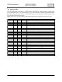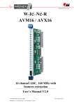
1
SIS Documentation
SIS3400 CDMSII
TDC/Time Stamper
SIS3400 CDMS II
VME TDC/Time Stamper
User Manual
SIS GmbH
Harksheider Str. 102A
22399 Hamburg
Germany
Phone: ++49 (0) 40 60 87 305 0
Fax:
++49 (0) 40 60 87 305 20
email: [email protected]
http://www.struck.de
Version: 1.20 as of 20.03.02
Page 1 of 47
SIS Documentation
SIS3400 CDMSII
TDC/Time Stamper
Revision Table:
Revision
0.1
1.0
1.01
1.02
1.03
1.10
Date
26.10.00
31.10.00
07.11.00
12.01.01
15.01.01
22.05.01
1.20
20.03.02
Page 2 of 47
Modification
Generation from SIS3400
First official release
Missing registers added, several additions
Experiment name fix -> CDMSII
Add missing control bits, add getting started table
Firmware version 0xA, FIFO word counter
time counter reset upon global reset
Firmware version 0xB
TIME_STAMP expanded to 32 bits
SIS Documentation
SIS3400 CDMSII
TDC/Time Stamper
1 Table of contents
1
2
3
Table of contents .............................................................................................................................................3
Introduction .....................................................................................................................................................5
Technical Properties/Features..........................................................................................................................6
3.1
Board Design ...........................................................................................................................................6
3.2
SIS3400 CDMS II input stage firmware..................................................................................................7
3.2.1
Clock Synchroniser/Clock receiver .................................................................................................8
4
Getting Started ...............................................................................................................................................10
5
Front Panel LEDs ..........................................................................................................................................11
6
Front Panel Control In/Outputs......................................................................................................................12
7
VME addressing ............................................................................................................................................13
7.1
Address Space........................................................................................................................................13
7.2
Base Address .........................................................................................................................................13
7.2.1
VME ..............................................................................................................................................13
7.3
Address Map..........................................................................................................................................14
8
Register Description ......................................................................................................................................16
8.1
Status Register (0x0)..............................................................................................................................16
8.2
Control Register (0x0) ...........................................................................................................................17
8.3
Module Identification and IRQ control register (0x4) ...........................................................................18
8.4
Formatter Control/Status Register (0x100)............................................................................................20
8.5
Formatter Module Address register (0x104)..........................................................................................21
8.6
FIFO Flag Register (0x108; read only)..................................................................................................21
8.7
FIFO Flag IRQ Enable register (0x10C)................................................................................................22
8.8
Output FIFO test registers (0x110 and 0x114) ......................................................................................23
8.8.1
Upper Test register for Output FIFO Test (0x110)........................................................................23
8.8.2
Lower Test register for Output FIFO Test (0x114) .......................................................................23
8.9
Output FIFO word counter (0x118).......................................................................................................23
8.10 Input group 1 Control/Status register (0x200) .......................................................................................24
8.11 Input inversion group 1 register (0x204) ...............................................................................................24
8.12 Input Group 1 FIFO test registers(0x210, 0x214, 0x218, 0x21C) .........................................................25
8.12.1 Test register 1 for Input FIFO Test (0x210) ................................................................................25
8.12.2 Test register 2 for Input FIFO Test (0x214) ................................................................................25
8.12.3 Test register 3 for Input FIFO Test (0x218) ................................................................................25
8.12.4 Test register 4 for Input FIFO Test (0x21C)................................................................................25
8.13 Input Buffer Group 1 registers (0x220, 0x224, 0x228, 0x22C).............................................................26
8.13.1 Input Buffer 1 (0x220).................................................................................................................26
8.13.2 Input Buffer 2 (0x224).................................................................................................................26
8.13.3 Input Buffer 3 (0x228).................................................................................................................26
8.13.4 Input Buffer 4 (0x22C) ................................................................................................................26
8.14 Time Shadow Registers (0x230, 0x234, 0x238, 0x23C) .......................................................................27
8.14.1 Time Shadow Register 1; (0x230) .................................................................................................27
8.14.2 Time Shadow Register 2 (0x234) ................................................................................................27
8.14.3 Time Shadow Register 3 (0x238) ................................................................................................27
8.14.4
Time Shadow Register 4 (0x23C)................................................................................................27
8.15 Input inversion group 2 register (0x204) ...............................................................................................28
8.16 Input Group 2 FIFO test registers (0x310, 0x314, 0x318, 0x31C) ........................................................29
8.16.1 Test register 5 for Input FIFO Test (0x310) ................................................................................29
8.16.2 Test register 6 for Input FIFO Test (0x314) ................................................................................29
8.16.3 Test register 7 for Input FIFO Test (0x318) ................................................................................29
8.16.4 Test register 8 for Input FIFO Test (0x31C)................................................................................29
8.17 Input Buffer Group 2 registers (0x320, 0x324, 0x328, 0x32C).............................................................30
8.17.1 Input Buffer 5 (0x320).................................................................................................................30
8.17.2 Input Buffer 6 (0x324).................................................................................................................30
8.17.3 Input Buffer 7 (0x328).................................................................................................................30
8.17.4 Input Buffer 8 (0x32C) ................................................................................................................30
8.18 Output FIFO (0x8000-0xFFFC or 0x10000 to 0x1FFFC) .....................................................................31
9
VME Interrupts..............................................................................................................................................32
10
Data Format ...............................................................................................................................................33
Page 3 of 47
SIS Documentation
SIS3400 CDMSII
TDC/Time Stamper
10.1 Single Wire mode ..................................................................................................................................33
10.2 Multiwire mode .....................................................................................................................................33
11
Input Configuration ...................................................................................................................................34
12
Connector Specification.............................................................................................................................34
13
Signal Specification ...................................................................................................................................35
13.1 Control Signals ......................................................................................................................................35
13.2 Inputs .....................................................................................................................................................35
14
Operating Conditions.................................................................................................................................35
14.1 Power Consumption/Voltage requirement.............................................................................................35
14.2 Cooling ..................................................................................................................................................35
14.3 Insertion/Removal..................................................................................................................................35
15
Test ............................................................................................................................................................36
15.1 LED (selftest).........................................................................................................................................36
15.2 FIFO tests ..............................................................................................................................................36
15.2.1
Input FIFO test...............................................................................................................................36
15.2.2
Output FIFO test ............................................................................................................................36
16
Software Support .......................................................................................................................................37
17
Appendix ...................................................................................................................................................38
17.1 Address Modifier Overview ..................................................................................................................38
17.2 Front Panel Layout.................................................................................................................................39
17.3 List of Jumpers and Switches ................................................................................................................40
17.3.1 J1 Addressing Mode Selection.......................................................................................................40
17.3.2
J34 Boot Mode and File Selection .................................................................................................40
17.3.3 SW1 and SW2 Base Address Selection .........................................................................................41
17.4 Board Layout .........................................................................................................................................42
17.5 FLASHPROM Versions ........................................................................................................................43
17.6 Row d and z Pin Assignments ...............................................................................................................44
17.7 Geographical Address Pin Assignments ................................................................................................45
17.8 Additional Information on VME ...........................................................................................................45
18
Index ..........................................................................................................................................................46
Page 4 of 47
SIS Documentation
SIS3400 CDMSII
TDC/Time Stamper
2 Introduction
The SIS3400 is a versatile 64 channel TTL or RS485 (CDMS II version) input module. The
card is a single width 6U VME board with hard metric coaxial input connectors. Possible
applications of the board comprise standard multi event latch, self triggering latch, trigger
time stamp generator and TDC for low speed applications.
Initially the development of the card was driven by the requirements of users from the
Neutron Scattering community in the context of the readout of a large scale Time Of Flight
(TOF) spectrometer at the Garching FRM II research reactor. As in the order of 14 front end
modules will be in use over a long time scale, design aspects like ease of maintenance and
minimum overhead system integration played an important role. The result are features like
hot swap and geographical addressing. To follow VMEs tradition of downward compatibility
cstandard VME addressing is implemented as well.
This manual describes the SIS3400 version, which was developed for the CDMS II
experiment, the main changes are SCSI style 68 pin input connectors in conjunction with
LEMO control connectors and RS485 level compatible receivers (TTL in the control case)
and a dedicated firmware design.
As we are aware, that no manual is perfect, we appreciate your feedback and will try to
incorporate proposed changes and corrections as quickly as possible. The most recent version
of this manual can be obtained by email from [email protected], the revision dates are online
under http://www.struck.de/manuals.htm. A list of available firmware designs can be
retrieved from http://www.struck.de/sis3400firm.htm
Page 5 of 47
SIS Documentation
SIS3400 CDMSII
TDC/Time Stamper
3 Technical Properties/Features
Find below a list of key features of the SIS3400 CDMSII.
• 64 channels
• 3 control in- and 3 control outputs
• 32-bit time bin counter with wrap around counter
• TTL level for control signals
• RS485 input level
• SCSI style 68-pin input connectors
• Derandomiser FIFO
• Output FIFO
• Leading Edge (input inversion through control register)
• FIFO and wrap around interrupts
• external/internal clock
• external/internal software inhibit
• software time reset/zero
• Up to four firmware files
• A24/32 D32/BLT32/MBLT64Geographical addressing mode (in conjunction with
VME64x backplane)
• Hot swap (in conjunction with VME64x backplane)
• VME64x Connectors
• VME64x Side Shielding
• VME64x Front panel
• VME64x extractor handles (on request)
• single supply (+5 V)
3.1 Board Design
As can be seen in the block diagram below, the SIS3400 is implemented as a two stage
FPGA-FIFO (Field Programmable Gate Array-First In First Out memory) design. The 64
input channels are connected to the three first stage FPGAs through input drivers. Depending
on the decision of the input stage FPGAs the 64-bit word and possibly additional information
like the event time stamp is stored in the input FIFO group (which consists of 5 18-bit x 64K
FIFO chips). The so called event formatter FPGA processes data from the input FIFOs and
stores the result in the output FIFOs. (the output FIFO group consists of 2 18-bit x 64K FIFO
chips) as long as the availability of sufficient space for the event is insured. Event processing
pauses as long as the FIFO almost full condition if flagged by the output FIFOs. If the VME
CPU side can not cope with the output data rate the input FIFO stage will finally reach the
almost full condition as well and the Veto output will be set.
Note:
the sustained input data rate of the input FPGAs of a SIS3400 which is clocked at 10 MHz
(100 ns time bins) is 80 Mbyte/s (8 byte x 10 MHz).
Page 6 of 47
SIS Documentation
SIS3400 CDMSII
TDC/Time Stamper
3.2 SIS3400 CDMS II input stage firmware
The SIS3400 CDMS II input stage firmware is edge sensitive. Input channels with a leading
edge within the time slice (clock cycle) will have their corresponding bit set in the input data
word. To allow for maximum flexibility the inputs can be inverted in the input stage FPGAs
via the two input stage inversion registers .
Data words with one or more leading edges will be stored in the input FIFO stage with the
corresponding counter value written to the time stamp FIFO upon the next leading edge of the
clock. While single wire and event mode are still available as formatter data handling options,
it is obvious, that no leading/trailing edge recognition is available. The formatter processing
time depends on the selected mode of operation. In multi wire mode it is in the order of 1 µs,
in single wire it is in the order of 5 µs. This value can be regarded as conversion time in
combination with the clock period. A module operated in event mode at a clock period of 1 µs
will have the event data stored in the output FIFO after some 2 µs. .
Note: Set Bits in the input stage Xilinx chips are cleared with the leading edge of the next
clock tick. During this process, which takes approximately 25 ns, a new leading edge may not
be detected, i.e. the safe double pulse resolution is clock + 25 ns.
Page 7 of 47
Boot
VME
Interface
Control
Control
VME Bus
SIS3400 CDMSII
TDC/Time Stamper
LEDs
SIS Documentation
Output FIFO
64K x 32-bit
Event Formatter
Derandomiser FIFO
64K x 64-bit
Frontend Logic
Inputs
Timestamp FIFO
64K x 20-bit
SIS3400 Block Diagram
3.2.1 Clock Synchroniser/Clock receiver
The first SIS3400 CDMSII in a multi module setup acts as the clock synchroniser, following
modules in the clock chain act as clock receiver modules. The power up default setting is
implemented in a fashion, that the unit will power up as clock synchroniser, what is the proper
setting for a single board. The clock synchroniser will synchronise start and stop signals (via
front panel or VME) to the negative edge of the clock and the positive clock edge will be used
to latch the data on the clock receiver modules to guarantee for synchronisation of all modules
in the chain. Starts and stops (by front panel as well as by VME) are synchronised to the clock
as shown in the scope shot below, the outgoing start/stop pulse has a width of one clock
period.
Note: The user has to make sure to provide a symmetric external clock (the internal 1 MHz
clock is symmetric)
Page 8 of 47
SIS Documentation
SIS3400 CDMSII
TDC/Time Stamper
The scope shot above shows the clock on the upper trace and the
synchronised start/stop pulse on the lower trace
Page 9 of 47
SIS Documentation
SIS3400 CDMSII
TDC/Time Stamper
4 Getting Started
The minimum setup to operate the SIS3400 CDMSII requires the following steps:
• Select the proper boot mode and firmware design with jumper J34
• Select the VME addressing mode with jumper J1
• Set the base address (if a non geographical addressing mode is used) with SW1 and SW2
• turn VME crate power off
• install the module in the VME crate
• turn crate power back on
• issue a key reset
• define clock receiver (if not first module in the chain)
• define clock source (1 MHz internal, 20 MHz internal, external or VME key)
• select input inversion inputs 64:33 and 32:1 (if required)
• select control input inversion (if required, see section 6)
• enable front panel control inputs
• select formatter mode (single wire e.g.)
• set formatter module address if desired
• enable input control logic (starts counter, arms for start/stop)
A good way of checking first time communication with the SIS3400 consists of switching on
the user LED by a write to the control register at offset address 0x0 with data word 0x1 (the
LED can be switched back off by writing 0x100 to the control register).
Getting started address/bit table:
Function
Key reset
Define clock receiver
(omit for first module in chain)
Define clock source
(omit for front panel clock or VME key))
Select input inversion inputs 64:33
(if required)
Select input inversion inputs 32
(if required)
Select control input inversion
(if required)
Enable front panel control inputs
(ored with VME control)
Select formatter mode (select single wire
mode, omit for multi wire mode)
Set formatter module address
(omit if 0 is fine with you)
Enable input control logic
Page 10 of 47
Address offset
0x20
0x0
Datum to write
arbitrary
0x40
0x0
0x204
0x8 (1 MHz)
0x4 (10 MHz)
0x1
0x304
0x1
0x0
0x50
0x0
0x10
0x100
0x1
0x104
0x0-0x1F
0x28
arbitrary
SIS Documentation
SIS3400 CDMSII
TDC/Time Stamper
5 Front Panel LEDs
The SIS3400 has 8 front panel LEDs to visualise part of the units status. Three LEDs
according to the VME64xP standard (Power, Access and Ready) plus 5 additional LEDs
(VME user LED, EVT, DIS, OVI and OVO LED).
Designation
A
P
R
U
EVT
LED
Access
Power
Ready
VME user LED
Event
Color
yellow
red
green
green
yellow
DIS
OVI
OVO
Disable
Overflow Input
Overflow Output
red
green
green
Function
Signals VME access to the unit
Flags presence of VME power
Signals configured logic
To be switched on/off under user program control
Signals one or more leading edges in time slice
(i.e. data word is copied to input FIFO)
Signals disabled or no gate present state
Signals input FIFO overflow
Signals output FIFO overflow
The LED locations are shown in the portion of the front panel drawing below.
The VME Access and the EVT LED are monostable (i.e. the duration of the on phase is
stretched for better visibility), the other LEDs reflect the current status.
An LED test cycle is performed upon power up (refer to chapter 15.1).
Page 11 of 47
SIS Documentation
SIS3400 CDMSII
TDC/Time Stamper
6 Front Panel Control In/Outputs
Six control signals are implemented in the SIS3400 CDMSII design, three inputs and three
outputs. Their location can be seen on the drawing above.
Input
Clock
Start
Stop
Output
Clock
Start
Stop
1
2
3
The input to output delay is approx. 15 ns.
Note: The internal clock will not be “seen” by the module if front panel input is enabled and
the external clock input is high (open and terminated with 4,7 KΩ to VCC e.g.). I.e. the
internal and external clock signals are ored). See section 8.2 for control input inversion
Page 12 of 47
SIS Documentation
SIS3400 CDMSII
TDC/Time Stamper
7 VME addressing
7.1 Address Space
Depending on the selected addressing mode the module occupies 16-bits (A24 mode) or 24bits (A32 mode) of the VME addressing space.
7.2
Base Address
7.2.1 VME
Besides standard A24 and A32 addressing the SIS3400 offers a pragmatic geographical
addressing mode. VIPA geographical addressing is foreseen as a possible future option, but
was considered too complex for the Neutron TOF application. The base address is defined by
the selected addressing mode, which is defined by jumper array J1 and possibly SW1 and
SW2 (in non geographical mode).
The table below summarises the possible base address settings.
x
Shorthand
SW1/SW2
GA0-GA4
0
x
GA0
0
GA3
GA1
0
GA4
0
0
0
GA2
0
not decoded
0
GA0
GA1
GA2
GA3
GA4
not decoded
0
x
0
x
0
x
0
x
0
set jumper(s) of J1
Address Bits
A32 A24 GEO VIPA 31 30 29 28 27 26 25 24 23 22 21 20 19 18 17 16
x
SW2
SW1
0
0
x
x
not decoded
not decoded
SW2
SW1
not implemented in current firmware
Explanation
Setting of rotary switch SW1 or SW2 respective
Geographical address bit as defined by the VME64x(P) backplane
The factory default setting for the SIS3400 CDMSII is shipped with SW2 set to 3 and SW1
set to 4 and A32 and A24 enabled, hence the module will respond to A32 0x34000000 and
A24 0x340000.
Page 13 of 47
SIS Documentation
SIS3400 CDMSII
TDC/Time Stamper
7.3 Address Map
The SIS3400 board is operated via VME registers and VME key address cycles, output data
are read from the FIFO. The following table gives an overview on all SIS3400 addresses and
their offset from the base address, a closer description of the registers and their function is
given in the following subsections.
Note: Write access to a key address (KA)with arbitrary data invokes the respective action
Offset
Key Access Type
0x000
0x004
R/W
R/W
D32
D32
Function
Control and Status register
Module Identification and IRQ control register
0x020
KA
W
D32
Global Reset (like Power On)
clear time counter also (from firmware rev. 0xA on)
0x028
0x02C
0x030
0x034
0x038
0x03C
KA
KA
KA
KA
KA
KA
W
W
W
W
W
W
D32
D32
D32
D32
D32
D32
Enable INPUT Control Logic
Disable INPUT Control Logic
Start (start of gate)
Stop (end of gate)
INPUT Control CLOCK pulse
INPUT Control CLEAR pulse (clears time counter)
KA
KA
R/W
R/W
R
R/W
R/W
R/W
R
W
W
D32
D32
D32
D32
D32
D32
D32
D32
D32
Formatter Control/Status register
Formatter Module Address register (module number)
FIFO Flag Status register
FIFO Flag IRQ Enable control register
Upper Test register for Output FIFO Test ;data bits [31:16]
Lower Test register for Output FIFO Test ;data bits [15:0]
Output FIFO word counter
Write test data into Output FIFO (if Test is enabled)
Clear all FIFOs and FIFO word counter
Formatter
0x100
0x104
0x108
0x10C
0x110
0x114
0x118
0x120
0x130
Page 14 of 47
SIS Documentation
SIS3400 CDMSII
TDC/Time Stamper
Input1
64-33
0x200
0x204
R/W
R/W
D32
D32
0x210
0x214
0x218
0x21C
0x220
0x224
0x228
0x22C
0x230
0x234
0x238
0x23C
R/W
R/W
R/W
R/W
R
R
R
R
R
R
R
R
D32
D32
D32
D32
D32
D32
D32
D32
D32
D32
D32
D32
0x304
R/W
D32
0x310
0x314
0x318
0x31C
0x320
0x324
0x328
0x32C
R/W
R/W
R/W
R/W
R
R
R
R
D32
D32
D32
D32
D32
D32
D32
D32
Input group 1 Control/Status register
Input inversion channel 63:32 Bit0=0 non inverting, Bit0=1
inverting
Test register 1 for Input FIFO Test; input data [64:57]
Test register 2 for Input FIFO Test; input data [56:49]
Test register 3 for Input FIFO Test; input data [48:41]
Test register 4 for Input FIFO Test; input data [40:33]
Input Buffer 1 ; input data [64:57]
Input Buffer 2 ; input data [56:49]
Input Buffer 3 ; input data [48:41]
Input Buffer 4 ; input data [40:33]
Time Shadow Register 1; Bits [64:57]
Time Shadow Register 2; Bits [56:49]
Time Shadow Register 3; Bits [48:41]
Time Shadow Register 4; Bits [40:33]
Input2
32-1
0x8000 to
0xFFFC
R
0x10000
to
0x1FFFC
R
Input inversion channel 32:1 Bit0=0 non inverting, Bit0=1
inverting
Test register 5 for Input FIFO Test; input data [32:25]
Test register 6 for Input FIFO Test; input data [24:17]
Test register 7 for Input FIFO Test; input data [16:9]
Test register 8 for Input FIFO Test; input data [8:1]
Input Buffer 5 ; input data [32:25]
Input Buffer 6 ; input data [24:17]
Input Buffer 7 ; input data [16:9]
Input Buffer 8 ; input data [8:1]
D32/
Output FIFO on A24 access
BLT32/
MBLT64
D32/
Output FIFO on A32 access
BLT32/
MBLT64
Note: D08 and D16 are not supported by the SIS3400 board
Page 15 of 47
SIS Documentation
SIS3400 CDMSII
TDC/Time Stamper
8 Register Description
8.1 Status Register (0x0)
The status register reflects the current settings of most of the SIS3400 parameters in read
access, in write access it functions as the control register.
Bit
31
30
29
28
27
26
25
24
23
22
21
20
19
18
17
16
15
14
13
12
11
10
9
8
7
6
5
4
3
2
1
0
Function
0
Status VME IRQ source 2 (test IRQ)
Status VME IRQ source 1 (ext. clock shadow)
Status VME IRQ source 0 (Overflow)
VME IRQ
internal VME IRQ
0
0
Status reserved 15
Status VME IRQ Enable Bit Source 2
Status VME IRQ Enable Bit Source 1
Status VME IRQ Enable Bit Source 0
Status reserved 11
Status reserved 10
Status reserved 9
Status reserved 8
Global INPUT Control Logic Enable bit
Gate (reflects current gate status)
0
0
0
0
0
0
Status input test
Status clock synchroniser
Status front panel input inversion
Status front panel control input
Status Enable 1 MHz CLOCK
Status Enable 10 MHz CLOCK
Status IRQ source 2 for software IRQ testing
Status user LED
The power up or key reset content is 0x0 (see default settings of control register).
Page 16 of 47
SIS Documentation
SIS3400 CDMSII
TDC/Time Stamper
8.2 Control Register (0x0)
The control register is in charge of the control of most of the basic properties of the SIS3400
board in write access. It is implemented via a selective J/K register, a specific function is
enabled by writing a 1 into the set/enable bit, the function is disabled by writing a 1 into the
clear/disable bit (which has a different location within the register). An undefined toggle
status will result from setting both the enable and disable bits for a specific function at the
same time.
On read access the same register represents the status register.
Bit
31
30
29
28
27
26
25
24
23
22
21
20
19
18
17
16
15
14
13
12
11
10
9
8
7
6
5
4
3
2
1
0
Function
clear reserved 15 (*)
disable IRQ source 2 (*)
disable IRQ source 1 (*)
disable IRQ source 0 (*)
clear reserved 11 (*)
clear reserved 10 (*)
clear reserved 9 (*)
clear reserved 8 (*)
set reserved 15
enable IRQ source 2 (test)
enable IRQ source 1 (input; counter IRQ; Counter overflow (toggle bit 20))
enable IRQ source 0 (formatter)
set reserved 11
set reserved 10
set reserved 9
set reserved 8
Disable input test (*)
Enable clock master (*)
Disable control input inversion (*)
Disable front panel control inputs (*)
Disable 1 MHz CLOCK (*)
Disable 10 MHz CLOCK (*)
clear IRQ test (source 2) (*)
switch off user LED (*)
Enable input test
Disable clock master
Enable control input inversion
Enable front panel control inputs
Enable 1 MHz CLOCK
Enable 10 MHz CLOCK
set IRQ test (source 2)
switch on user LED
(*) denotes the default power up or key reset state
Page 17 of 47
SIS Documentation
SIS3400 CDMSII
TDC/Time Stamper
8.3 Module Identification and IRQ control register (0x4)
This register has two basic functions. The first is to give information on the active firmware
design. This function is implemented via the read only upper 20 bits of the register. Bits 1631 hold the four digits of the SIS module number (like 3400 e.g.), bits 12-15 hold the version
number. The version number allows a distinction between different implementations of the
same module number, the SIS3400 for example has the frontend module mode and the clock
module mode as versions.
Control register bit assignment table:
Bit
31
30
29
28
27
26
25
24
23
22
21
20
19
18
17
16
15
14
13
12
11
10
9
8
7
6
5
4
3
2
1
0
Read/Write access
read only
read only
read only
read only
Read only
read only
read only
read only
read only
read only
read only
read only
read only
read only
read only
read only
read only
read only
read only
read only
read/write
read/write
read/write
read/write
read/write
read/write
read/write
read/write
read/write
read/write
read/write
read/write
Page 18 of 47
Function
Module Identification Bit 15
Module Id Digit 3
Module Identification Bit 14
Module Identification Bit 13
Module Identification Bit 12
Module Identification Bit 11
Module Id Digit 2
Module Identification Bit 10
Module Identification Bit 9
Module Identification Bit 8
Module Identification Bit 7
Module Id Digit 1
Module Identification Bit 6
Module Identification Bit 5
Module Identification Bit 4
Module Identification Bit 3
Module Id Digit 0
Module Identification Bit 2
Module Identification Bit 1
Module Identification Bit 0
Version Bit 3
Version Bit 2
Version Bit 1
Version Bit 0
VME IRQ Enable (0=IRQ disabled, 1=IRQ enabled)
VME IRQ Level Bit 2
VME IRQ Level Bit 1
VME IRQ Level Bit 0
IRQ Vector Bit 7; placed on D7 during VME IRQ ACK cycle
IRQ Vector Bit 6; placed on D6 during VME IRQ ACK cycle
IRQ Vector Bit 5; placed on D5 during VME IRQ ACK cycle
IRQ Vector Bit 4; placed on D4 during VME IRQ ACK cycle
IRQ Vector Bit 3; placed on D3 during VME IRQ ACK cycle
IRQ Vector Bit 2; placed on D2 during VME IRQ ACK cycle
IRQ Vector Bit 1; placed on D1 during VME IRQ ACK cycle
IRQ Vector Bit 0; placed on D0 during VME IRQ ACK cycle
SIS Documentation
SIS3400 CDMSII
TDC/Time Stamper
The second function of the register is interrupt control. The interrupter type of the SIS3400 is
D08(O) ROAK . Via bits 0-7 of the module identifier and interrupt control register you can
define the interrupt vector, which is placed on the VME bus during the interrupt acknowledge
cycle. Bits 8 through 10 define the VME interrupt level, bit 11 is used to enable (bit set to 1)
or disable (bit set to 0) interrupting.
Module identification and version example:
The register for a SIS3400 CDMSII reads 0x3400Bnnn (the status of the lower 3 nibbles is
denoted with n in the example).
Page 19 of 47
SIS Documentation
SIS3400 CDMSII
TDC/Time Stamper
8.4 Formatter Control/Status Register (0x100)
The behaviour of the event formatter can be controlled through this register. On read access
the register represents the formatter status register.
Bit
31
..
..
16
15
14
13
12
11
10
9
8
7
6
5
4
3
2
1
0
Read/Write access
read only
..
..
read only
read/write
read/write
read/write
read/write
read/write
read/write
read/write
read/write
read/write
read/write
read/write
Read/write
read/write
read/write
Read/write
Read/write
Function
No function ; read “0”
No function ; read “0”
reserved
reserved
reserved
reserved
reserved
reserved
reserved
reserved
reserved
reserved
reserved
OUTPUT_FIFO_TEST Mode
reserved
reserved
reserved
single wire mode (else multi wire mode if 0)
Power up default reading: 0x00000000
Page 20 of 47
SIS Documentation
SIS3400 CDMSII
TDC/Time Stamper
8.5 Formatter Module Address register (0x104)
This read/write register defines the address, which is copied into the output FIFO data stream
of the SIS3400. In a multi module setup a detector channel is identified by its channel number
(0-63) and its formatter module address (0-15), i.e. up to 1024 detector channels can be
identified in a unique fashion without additional data to be added by the VME CPU.
Bit
31
..
..
8
7
6
5
4
3
2
1
0
Read/Write access
read only
..
..
read only
read only
read only
read only
read/write
read/write
read/write
read/write
read/write
Function
No function ; read “0”
No function ; read “0”
No function ; read “0”
No function ; read “0”
No function ; read “0”
Module Address Bit 4 (used in data stream)
Module Address Bit 3 (used in data stream)
Module Address Bit 2 (used in data stream)
Module Address Bit 1 (used in data stream)
Module Address Bit 0 (used in data stream)
The power up value of the register is: 0x00000000
8.6 FIFO Flag Register (0x108; read only)
The status of the input FIFO group and the output FIFO group can be retrieved from this read
only register. In most cases the evaluation of the FIFO flag register of all frontend modules
will be a good way to control overall readout. As an alternative the FIFO flags can be used to
generate interrupts with the interrupt service routine handling readout.
Bit
31
..
..
16
15
14
13
12
11
10
9
8
7
6
5
4
3
2
1
0
Read Function
0
0
0
0
0
Input FIFO flag full
Input FIFO flag almost full
Input FIFO flag half full
Input FIFO flag almost empty
Input FIFO flag empty
0
0
0
Output FIFO flag full
Output FIFO flag almost full
Output FIFO flag half full
Output FIFO flag almost empty
Output FIFO flag empty
The reading of the status register after power up or key reset is 0x303
Page 21 of 47
SIS Documentation
SIS3400 CDMSII
TDC/Time Stamper
8.7 FIFO Flag IRQ Enable register (0x10C)
This read/write register defines which condition(s) of the output FIFO will generate an
interrupt for interrupt driven readout applications. The optimum setting will depend on
application, data rate and performance of the VME master.
Bit
31
..
..
16
15
14
13
12
11
10
9
8
7
6
5
4
3
2
1
0
Read/Write access
read only
..
..
read only
read/write
read/write
read/write
read/write
read/write
read/write
read/write
Read/write
Read/write
Read/write
Read/write
Read/write
Read/write
Read/write
Read/write
Read/write
Function
No function ; read “0”
No function ; read “0”
reserved
reserved
reserved
reserved
reserved
reserved
reserved
reserved
reserved
reserved
reserved
Enable IRQ if Output FIFO is full
Enable IRQ if Output FIFO is almost full
Enable IRQ if Output FIFO is half full
Enable IRQ if Output FIFO is NOT almost empty
Enable IRQ if Output FIFO is NOT empty
Power up default value: 0x00000000
Page 22 of 47
SIS Documentation
SIS3400 CDMSII
TDC/Time Stamper
8.8 Output FIFO test registers (0x110 and 0x114)
Data can be written to the 32-bit wide output FIFO through the upper and lower test register if
output FIFO test mode is enabled. . To transfer the data of the two test registers to the FIFO a
key address cycle to address 0x120 is required.
8.8.1 Upper Test register for Output FIFO Test (0x110)
Bit
31
..
..
16
15
..
..
0
Read/Write access
Read only
..
..
Read only
Read/write
..
..
Read/write
Function
No function ; read “0”
No function ; read “0”
Output Fifo Test Data Bit 31
Output Fifo Test Data Bit 16
Power up default value: 0x00000000
8.8.2 Lower Test register for Output FIFO Test (0x114)
Bit
31
..
..
16
15
..
..
0
Read/Write access
read only
..
..
read only
read/write
..
..
read/write
Function
No function ; read “0”
No function ; read “0”
Output Fifo Test Data Bit 15
Output Fifo Test Data Bit 0
after power up: 0x00000000
8.9 Output FIFO word counter (0x118)
The read only, 16-bit wide, output FIFO word counter is incremented with every word stored
in the output FIFO. It is reset upon global reset (KA 0x20) or the clear all FIFO (KA 0x130)
command.
Page 23 of 47
SIS Documentation
SIS3400 CDMSII
TDC/Time Stamper
8.10 Input group 1 Control/Status register (0x200)
The contents of the time shadow register can be frozen for readout by setting bit 0 of the
input group control register to ensure, that no changes occur while the actual time value is
read from time shadow registers 1 through 4.
Note: there is no equivalent group 2 register.
Bit
31
..
..
8
7
6
5
4
3
2
1
0
Read/Write access
read only
..
..
read only
read/write
read/write
read/write
read/write
read/write
read/write
read/write
read/write
Function
No function; read as 0
No function; read as 0
reserved, read as 0
reserved, read as 0
reserved, read as 0
reserved, read as 0
reserved, read as 0
reserved, read as 0
reserved, read as 0
TIME Shadow Register freeze bit
The power up reading is: 0x00000000
8.11 Input inversion group 1 register (0x204)
After power up the SIS3400 CDMS II latches leading edge transitions as “1”. Trailing edges
can be selected for input channels 64 to 33 by setting bit 0 of this register.
Bit
31
..
..
8
7
6
5
4
3
2
1
0
Read/Write access
read only
..
..
read only
read/write
read/write
read/write
read/write
read/write
read/write
read/write
read/write
Function
No function; read as 0
No function; read as 0
reserved, read as 0
reserved, read as 0
reserved, read as 0
reserved, read as 0
reserved, read as 0
reserved, read as 0
reserved, read as 0
Input group 1 (channels 64:33) inversion mode
The power up reading is: 0x00000000
Page 24 of 47
SIS Documentation
SIS3400 CDMSII
TDC/Time Stamper
8.12 Input Group 1 FIFO test registers(0x210, 0x214, 0x218, 0x21C)
Data can be written to the input FIFO through the four input group1 FIFO test registers and
the four input group 2 FIFO test registers. The data are copied to the input FIFO with a key
address 0x38 access if input control mode 3 is avtive.
8.12.1 Test register 1 for Input FIFO
Test (0x210)
8.12.3 Test register 3 for Input FIFO
Test (0x218)
Bit
31
..
..
8
7
..
..
0
Bit
31
..
..
8
7
..
..
0
Read/Write access
Read only
..
..
Read only
Read/write
..
..
Read/write
Function
No function ; read “0”
No function ; read “0”
Input Fifo Test Data Bit 63
Input Fifo Test Data Bit 56
Read/Write access
Read only
..
..
Read only
Read/write
..
..
Read/write
Function
No function ; read “0”
No function ; read “0”
Input Fifo Test Data Bit 47
Input Fifo Test Data Bit 40
after power up: 0x00000000
after power up: 0x00000000
8.12.2 Test register 2 for Input FIFO
Test (0x214)
8.12.4 Test register 4 for Input FIFO
Test (0x21C)
Bit
31
..
..
8
7
..
..
0
Bit
31
..
..
8
7
..
..
0
Read/Write access
Read only
..
..
Read only
Read/write
..
..
Read/write
Function
No function ; read “0”
No function ; read “0”
Input Fifo Test Data Bit 55
Input Fifo Test Data Bit 48
after power up: 0x00000000
Read/Write access
Read only
..
..
Read only
Read/write
..
..
Read/write
Function
No function ; read “0”
No function ; read “0”
Input Fifo Test Data Bit 39
Input Fifo Test Data Bit 32
after power up: 0x00000000
Page 25 of 47
SIS Documentation
SIS3400 CDMSII
TDC/Time Stamper
8.13 Input Buffer Group 1 registers (0x220, 0x224, 0x228, 0x22C)
The status of the 64 inputs can be read in groups of 8-bit through the four input buffer group 1
and the four input buffer group 2 (read only) registers for test purposes.
8.13.1 Input Buffer 1 (0x220)
8.13.3 Input Buffer 3 (0x228)
Bit
31
..
..
8
7
..
..
0
Bit
31
..
..
8
7
..
..
0
Read/Write access
Read only
..
..
Read only
Read only
..
..
Read only
Function
No function ; read “0”
No function ; read “0”
Input Buffer Data Bit 63
Input Buffer Data Bit 56
Read/Write access
Read only
..
..
Read only
Read only
..
..
Read only
Function
No function ; read “0”
No function ; read “0”
Input Buffer Data Bit 47
Input Buffer Data Bit 40
8.13.2 Input Buffer 2 (0x224)
8.13.4 Input Buffer 4 (0x22C)
Bit
31
..
..
8
7
..
..
0
Bit
31
..
..
8
7
..
..
0
Read/Write access
Read only
..
..
Read only
Read only
..
..
Read only
Page 26 of 47
Function
No function ; read “0”
No function ; read “0”
Input Buffer Data Bit 55
Input Buffer Data Bit 48
Read/Write access
Read only
..
..
Read only
Read only
..
..
Read only
Function
No function ; read “0”
No function ; read “0”
Input Buffer Data Bit 39
Input Buffer Data Bit 32
SIS Documentation
SIS3400 CDMSII
TDC/Time Stamper
8.14 Time Shadow Registers (0x230, 0x234, 0x238, 0x23C)
The 32-bit wide time stamp can be read trough the four (read only) time shadow registers. To
avoid incorrect reading caused by toggling bits, it is recommended to freeze the time shadow
register by setting bit 0 of the input group control register, to read the time from the four time
shadow registers and to unfreeze the time shadow register by clearing bit 0 of the input group
control register again.
The time shadow register is updated with every clock tick as long as bit 0 of the input group
control register is cleared.
8.14.1 Time Shadow Register 1;
(0x230)
8.14.3 Time Shadow Register 3
(0x238)
Bit
31
..
..
8
7
..
..
0
Bit
31
..
..
8
7
..
..
0
Function
No function ; read “0”
No function ; read “0”
Time Shadow Register Bit 31
Time Shadow Register Bit 24
Function
No function ; read “0”
No function ; read “0”
Time Shadow Register Bit 15
Time Shadow Register Bit 8
8.14.2 Time Shadow Register 2
(0x234)
8.14.4 Time Shadow Register 4
(0x23C)
Bit
31
..
..
8
7
..
..
0
Bit
31
..
..
8
7
..
..
0
Function
No function ; read “0”
No function ; read “0”
Time Shadow Register Bit 23
Time Shadow Register Bit 16
Function
No function ; read “0”
No function ; read “0”
Time Shadow Register Bit 7
Time Shadow Register Bit 0
Page 27 of 47
SIS Documentation
SIS3400 CDMSII
TDC/Time Stamper
8.15 Input inversion group 2 register (0x204)
After power up the SIS3400 CDMS II latches leading edge transitions as “1”. Trailing edges
can be selected for input channels 32 to 1 by setting bit 0 of this register.
Bit
31
..
..
8
7
6
5
4
3
2
1
0
Read/Write access
read only
..
..
read only
read/write
read/write
read/write
read/write
read/write
read/write
read/write
read/write
Function
No function; read as 0
No function; read as 0
reserved, read as 0
reserved, read as 0
reserved, read as 0
reserved, read as 0
reserved, read as 0
reserved, read as 0
reserved, read as 0
Input group 1 (channels 32:1) inversion mode
The power up reading is: 0x00000000
Page 28 of 47
SIS Documentation
SIS3400 CDMSII
TDC/Time Stamper
8.16 Input Group 2 FIFO test registers (0x310, 0x314, 0x318, 0x31C)
8.16.1 Test register 5 for Input FIFO
Test (0x310)
8.16.3 Test register 7 for Input FIFO
Test (0x318)
Bit
31
..
..
8
7
..
..
0
Bit
31
..
..
8
7
..
..
0
Read/Write access
Read only
..
..
Read only
Read/write
..
..
Read/write
Function
No function ; read “0”
No function ; read “0”
Input Fifo Test Data Bit 31
Input Fifo Test Data Bit 24
Read/Write access
Read only
..
..
Read only
Read/write
..
..
Read/write
Function
No function ; read “0”
No function ; read “0”
Input Fifo Test Data Bit 15
Input Fifo Test Data Bit 8
after power up: 0x00000000
after power up: 0x00000000
8.16.2 Test register 6 for Input FIFO
Test (0x314)
8.16.4 Test register 8 for Input FIFO
Test (0x31C)
Bit
31
..
..
8
7
..
..
0
Bit
31
..
..
8
7
..
..
0
Read/Write access
Read only
..
..
Read only
Read/write
..
..
Read/write
Function
No function ; read “0”
No function ; read “0”
Input Fifo Test Data Bit 23
Input Fifo Test Data Bit 16
after power up: 0x00000000
Read/Write access
Read only
..
..
Read only
Read/write
..
..
Read/write
Function
No function ; read “0”
No function ; read “0”
Input Fifo Test Data Bit 7
Input Fifo Test Data Bit 0
after power up: 0x00000000
Page 29 of 47
SIS Documentation
SIS3400 CDMSII
TDC/Time Stamper
8.17 Input Buffer Group 2 registers (0x320, 0x324, 0x328, 0x32C)
8.17.1 Input Buffer 5 (0x320)
8.17.3 Input Buffer 7 (0x328)
Bit
31
..
..
8
7
..
..
0
Bit
31
..
..
8
7
..
..
0
Read/Write access
Read only
..
..
Read only
Read only
..
..
Read only
Function
No function ; read “0”
No function ; read “0”
Input Buffer Data Bit 31
Input Buffer Data Bit 24
Read/Write access
Read only
..
..
Read only
Read only
..
..
Read only
Function
No function ; read “0”
No function ; read “0”
Input Buffer Data Bit 15
Input Buffer Data Bit 8
8.17.2 Input Buffer 6 (0x324)
8.17.4 Input Buffer 8 (0x32C)
Bit
31
..
..
8
7
..
..
0
Bit
31
..
..
8
7
..
..
0
Read/Write access
Read only
..
..
Read only
Read only
..
..
Read only
Page 30 of 47
Function
No function ; read “0”
No function ; read “0”
Input Buffer Data Bit 23
Input Buffer Data Bit 16
Read/Write access
Read only
..
..
Read only
Read only
..
..
Read only
Function
No function ; read “0”
No function ; read “0”
Input Buffer Data Bit 7
Input Buffer Data Bit 0
SIS Documentation
SIS3400 CDMSII
TDC/Time Stamper
8.18 Output FIFO (0x8000-0xFFFC or 0x10000 to 0x1FFFC)
The address range of the output FIFO (First In First Out) depends on the addressing mode.
Mode
A24
A32
FIFO Address range
0x8000-0x8FFFC
0x10000-0x1FFFC
The output FIFO consists of two 64Kx18-bit FIFO chips, which are used in parallel to hold
the formatted 32-bit wide output word. Normally one address to read from would be sufficient
for the FIFO, but as most VME masters use address auto increment on block transfers, a
contiguous address block allows for more efficient readout. The address range was chosen in
a fashion, that allows for the readout of half of the FIFO in one block read (which typically
consists of many 256 Byte reads on the VME bus) if A32 addressing is used. Hence A32 is
the preferred addressing mode in high speed readout applications.
The data format of the output FIFO data is described in section 10.
Note: read access to the empty output FIFO results in a bus error (BERR)
Page 31 of 47
SIS Documentation
SIS3400 CDMSII
TDC/Time Stamper
9 VME Interrupts
Three VME interrupt sources are implemented in the SIS3400 firmware design:
• output FIFO flag
• 20-bit counter roll over
• test
For compatibility with the LINUX Universe driver, the interrupts were implemented in
release on acknowledge (ROAK) style .
Interrupt generation has to be enabled by setting bit 11 in the IRQ and version register. The
internal VME interrupt flag can be used to check on an IRQ condition without actually
making use of interrupts on the bus.
The VME interrupt level (1-7) are defined by bits 8 through 10 and the VME interrupt vector
(0-255) by bits 0 through 7 of the VME IRQ and version register.
Find a diagram with the overall interrupt mechanism of the SIS3400 below
Internal IRQ
Test
Enable 2
20-bit toggle
clear
Enable 1
FIFO
Flags
Enable 0
IRQ ACK
Enable IRQ
Page 32 of 47
clear
enable
register
VME IRQ
SIS Documentation
SIS3400 CDMSII
TDC/Time Stamper
10 Data Format
At present two formatter data formats are implemented, the so called single wire mode and
the so called event mode. In single wire mode two 32-bit words per hit (i.e. bit change 0→1)
are written to the output FIFO .
The new status of all 64 input bits is written to the output FIFO in multi wire mode. Two
more 32-bit words are needed to hold time and module Id. information.
Note: The output FIFO can be read in D32, BLT32 and MBLT32
10.1 Single Wire mode
32-bit word
bit 31
bits 30-26
bits 25-20
bits 19-0
1
Trailing (always 1)
Module Id.
Channel
0
2
Time Stamp (31-0)
10.2 Multiwire mode
32-bit word
bit 31
bits 30-26
bits 25-20
bits 19-0
1
0
Module Id.
0
0
2
Time Stamp (bits 31-0)
3
Input Bits 63-32 (channels 64-33) (bits 31-0)
4
Input Bits 31-0 (channels 32-1) (bits 31-0)
Page 33 of 47
SIS Documentation
SIS3400 CDMSII
TDC/Time Stamper
11 Input Configuration
SIS3400 CDMS II boards can be configured for TTL control levels with 50 Ohm or high
impedance input termination and 100 Ohm or high impedance (resistor networks removed,
recommended for daisy chaining only) RS485 inputs . The resistor networks are in sockets.
For low active input levels the signals can be connected to VCC through RN1B to RN18B with
1 KΩ.
Network
RN1A
RN1B
RN1C
RN5A, 5B, 6A, 6B
RN7A, 7B, 8A, 8B
RN9A, 9B, 10A, 10B
RN11A, 11B, 12A, 12B
RN13A, 13B, 14A, 14B
RN15A,15B, 16A, 16B
RN17A, 17B, 18A, 18B
RN19A, 19B, 20A, 20B
Channels
Control Input 1
Control Input 2
Control Input 3
1,2 3,4 5,6 7,8
9,10 11,12 13,14 15,16
17,18 19,20 21,22 23,24
25,26 27,28 29,30 31,32
33,34 35,36 37,38 39,40
41,42 43,44 45,46 47,48
49,50 51,52 53,54 55,56
57,58 59,60 61,62 63,64
12 Connector Specification
The two different types of front panel and VME connectors used on the SIS3400 CDMS II
are:
Connector
160 pin zabcd
LEMO00
68-pin
Page 34 of 47
Purpose
VME P1/P2
Control in/output
Input
Part Number
Harting 02 01 160 2101
LEMO EPB.00.250.NTN
Thomas&Betts
HFR068RA29JSI
SIS Documentation
SIS3400 CDMSII
TDC/Time Stamper
13 Signal Specification
13.1 Control Signals
The width of the start and stop pulse has to be greater or equal 15 ns, the maximum external
clock shall not exceed 10 MHz, the wave form has to be symmetric.
13.2 Inputs
The SIS3400 control section is designed for high active TTL inputs, by default the module is
shipped with 50 Ohm input termination.
Logic Level
0
1
Level in V
< 0,8
> 2,4
The forbidden range between the high and low level can result in undefined states.
If 1K input termination is chosen, open inputs will be seen as “1”, control input inversion can
be used to redefine them as “0”.
SIS3400 CDMS II inputs are designed for RS485 levels, the receiver input sensitivity is +/200 mV (refer to www.rs485.com for details). .
14 Operating Conditions
14.1 Power Consumption/Voltage requirement
To allow for the use of the SIS3400 independent of the users VME crate no non standard
voltage is used by the board. In especial the card is a single supply (+5 V) design. The +3.3 V
supply voltage for the on board FPGAs is generated by linear regulators. The actual power
consumption of the module will vary with input data rate and may also depend on the actual
firmware.
Operating conditions
SIS3400 Idle
SIS3400-Clock 20 MHz
SIS3400 CDMSII Idle
Voltage in V Current in A
+5
2,2
+5
+5
2,4
14.2 Cooling
Forced air flow is required for the operation of the SIS3400 board.
14.3 Insertion/Removal
Please note, that the VME standard does not support live insertion (hot swap). Hence crate
power has to be turned off for installation and removal of SIS3400s in standard VME crates.
The leading pins on the SIS3400 VME64x VME connectors and connected on board circuitry
are designed for hot swap in conjunction with a VME64x backplane (a VME64x backplane
can be recognised by the 5 row VME connectors, while the standard VME backplane has
three row connectors only).
Page 35 of 47
SIS Documentation
SIS3400 CDMSII
TDC/Time Stamper
15 Test
The SIS3400 provides a number of test features, which allow for debugging of the unit as
well as for overall system setup tests.
15.1 LED (selftest)
During power up self test and LCA configuration all LEDs except the Ready (R) LED are on.
After the initialisation phase is completed, all LEDs except the Ready (R), Power (P) and
Disable (DIS) LED have to go off. Differing behaviour indicates either a problem with the
download of the firmware boot file or one or more LCA and/or the download logic.
15.2 FIFO tests
15.2.1 Input FIFO test
Defined input data can be written to the input FIFO chips from VME when input mode 3 is
selected via the control register. The data have to be written to the 8 input group 1/group 2
FIFO test registers and are transferred to the input FIFO chips upon a key address access to
0x38.(input control clock pulse).
15.2.2 Output FIFO test
The output FIFO chips can be tested in the same fashion as the input FIFO. Data are clocked
into the output FIFO chips with a key address cycle to address 0x120 from the upper and
lower output FIFO test registers. The test mode is enabled when input control mode 3 is
activated.
Page 36 of 47
SIS Documentation
SIS3400 CDMSII
TDC/Time Stamper
16 Software Support
The first application of the SIS3400 was the FRM II TOF spectrometer readout system. A
readout program with external configuration was developed for Dr. Jürgen Hannappels
Universe II driver. The SBS-OR VP7 VME PC was used as platform, the driver has been
tested with other Tundra Universe II based VME PCs also.
The latest CDMS II firmware version was tested with a PC and the SIS1100/3100 PCI to
VME interface under LINUX.
The software for both systems will be provided on request by email or on disk. In addition the
LINUX PCI to VME interface code will work with minimum modifications with the
Windows 2000 driver for the SIS1100/3100 interface also..
Page 37 of 47
SIS Documentation
SIS3400 CDMSII
TDC/Time Stamper
17 Appendix
17.1 Address Modifier Overview
Find below the table of address modifiers, which can be used with the SIS3400 (with the
corresponding addressing mode enabled).
AM code
0x3F
0x3D
0x3C
0x3B
0x39
0x38
0x0F
0x0D
0x0C
0x0B
0x09
0x08
Page 38 of 47
Mode
A24 supervisory block transfer (BLT)
A24 supervisory data access
A24 supervisory 64-bit block transfer (MBLT)
A24 non-privileged block transfer (BLT)
A24 non-privileged data access
A24 non-privileged 64-bit block transfer (MBLT)
A32 supervisory block transfer (BLT)
A32 supervisory data access
A32 supervisory 64-bit block transfer (MBLT)
A32 non-privileged block transfer (BLT)
A32 non privileged data access
A32 non privileged 64-bit block transfer (MBLT)
SIS Documentation
SIS3400 CDMSII
TDC/Time Stamper
17.2 Front Panel Layout
The front panel of the SIS3400 CDMS II is equipped with 8 LEDs, 6 control in- and outputs
and 64 inputs. The control connectors are of LEMO00 style, the two input connectors are of
68-pin SCSI -style . The units are 4 TE (one VME slot) wide, the front panel is of EMC
shielding type. VME64x/VIPA extractor handles are available on request or can be retrofitted
by the user, if he wants to change to a VME64x/VIPA crate at a later point in time.
In the drawing below you can find the front panel layout.
Note: Only the aluminium portion without the extractor handle mounting fixtures is
shown
Page 39 of 47
SIS Documentation
SIS3400 CDMSII
TDC/Time Stamper
17.3 List of Jumpers and Switches
Find below a list of jumpers and switches.
Name
J1
J34
SW1
SW2
Type
Array
Array
Rotary
Rotary
Function
Addressing mode selection
Boot mode selection
Base address setting
Base address setting
17.3.1 J1 Addressing Mode Selection
As described in section 7.2, the SIS3400 supports several addressing modes, the actual mode
is selected by jumper array J1. The given mode is selected if ist corresponding jumper is in
place. The four jumper positions are described in the table below.
J1
A32
A24
GEO
VIPA
Jumper
A32
A24
GEO
VIPA
Function
enable A32 addressing
enable A32 addressing
enable geographical addressing
not implemented yet
Factory default
closed
closed
open
open
Note: It is possible to have A32 and A24 set in parallel. If an A32 cycle is detected in this
case, the setting of SW1 and SW2 is compared with A31-A24, if an A24 cycle is detected,
SW1 and SW2 are compared with A23-A16.
17.3.2 J34 Boot Mode and File Selection
The firmware of the SIS3400 can be loaded off a FLASHPROM or via JTAG. In
FLASHPROM boot mode up to four different boot files can be selected with the possible
combinations of jumpers M3 and M4.
J34
M1
M2
M3
M4
Jumper
M1
M2
M3
M4
Function
Reserved
Boot mode selection (closed FLASH, open JTAG)
Boot file Bit0 (closed = 0, open =1)
Boot file Bit1 (closed = 0, open =1)
Factory default
closed
closed
closed
closed
Note: The factory default setting (M2, M3 and M4 closed) boots file 0 from the
FLASHPROM. For the SIS3400 clock distribution firmware the setting is M2 closed, M3
open, M4 closed (boot file 1 from FLASH).
Page 40 of 47
SIS Documentation
SIS3400 CDMSII
TDC/Time Stamper
17.3.3 SW1 and SW2 Base Address Selection
The two hexadecimal rotary switches SW1 and SW2 are used to define the VME base address
in systems without geographical addressing capabilities (i.e. if standard VME crates are used).
The two switches are labelled ADR_LO (SW1) and ADR_UP (SW2), as they define the
lower and upper address nibble of the eight leading address bits (A31 to A24 with A32
enabled and addressed, A23 to A16 with A24 enabled and addressed). The setting of the two
switches is ignored if a geographical addressing mode (GEO or VIPA) is enabled.
Page 41 of 47
SIS Documentation
17.4 Board Layout
Page 42 of 47
SIS3400 CDMSII
TDC/Time Stamper
SIS Documentation
SIS3400 CDMSII
TDC/Time Stamper
17.5 FLASHPROM Versions
A list of available FLASHPROMs can be obtained from
http://www.struck.de/sis3400firm.htm. Please note, that a special hardware configuration may
be necessary for the firmware design of interest.
The table on the web is of the format shown below:
SIS3400 FLASHPROM table
Design Name
SIS3400_020300
SIS3400_200400
SIS3400_271000
SIS3400_070501
SIS3400_200302
Design
0
0
0
0
0
Boot File (s)
SIS3400 Version 1
SIS3400 Version 2 (clock module)
SIS3400 Version 9 (CDMS II)
SIS3400 Version 0xA (CDMS II)
SIS3400 Version 0xB (CDMS II)
Page 43 of 47
SIS Documentation
SIS3400 CDMSII
TDC/Time Stamper
17.6 Row d and z Pin Assignments
The SIS3400 is ready for the use with VME64x and VME64xP backplanes. Features include
geographical addressing and live insertion (hot swap). The prepared/used pins on the d and z
rows of the P1 and P2 connectors are listed below.
Position
P1/J1
Row z
1
2
3
4
5
6
7
8
9
10
11
12
13
14
15
16
17
18
19
20
21
22
23
24
25
26
27
28
29
30
31
32
GND
P2/J2
Row d
VPC (1)
GND (1)
Row z
GND
GND
GND
GND
GND
GND
GND
RESP*
GND
Row d
GND
GAP*
GA0*
GA1*
GND
GND
GA2*
GND
GND
GA3*
GND
GND
GA4*
GND
GND
GND
GND
GND
GND
GND
GND
GND
GND
GND
GND
GND
GND
GND
GND (1)
VPC (1)
GND
GND (1)
VPC (1)
Note: Pins designated with (1) are so called MFBL (mate first-break last) pins on the installed 160 pin
connectors, VPC(1) pins are connected via inductors.
Page 44 of 47
SIS Documentation
SIS3400 CDMSII
TDC/Time Stamper
17.7 Geographical Address Pin Assignments
The SIS3400 board can be used with geographical addressing via the geographical address
pins GA0*, GA1*, GA2*, GA3*, GA4* and GAP*. The address pins are left open or tied to
ground by the backplane as listed in the following table:
Slot
Number
1
2
3
4
5
6
7
8
9
10
11
12
13
14
15
16
17
18
19
20
21
GAP*
Pin
Open
Open
GND
Open
GND
GND
Open
Open
GND
GND
Open
GND
Open
Open
GND
Open
GND
GND
Open
GND
Open
GA4*
Pin
Open
Open
Open
Open
Open
Open
Open
Open
Open
Open
Open
Open
Open
Open
Open
GND
GND
GND
GND
GND
GND
GA3*
Pin
Open
Open
Open
Open
Open
Open
Open
GND
GND
GND
GND
GND
GND
GND
GND
Open
Open
Open
Open
Open
Open
GA2*
Pin
Open
Open
Open
GND
GND
GND
GND
Open
Open
Open
Open
GND
GND
GND
GND
Open
Open
Open
Open
GND
GND
GA1*
Pin
Open
GND
GND
Open
Open
GND
GND
Open
Open
GND
GND
Open
Open
GND
GND
Open
Open
GND
GND
Open
Open
GA0*
Pin
GND
Open
GND
Open
GND
Open
GND
Open
GND
Open
GND
Open
GND
Open
GND
Open
GND
Open
GND
Open
GND
17.8 Additional Information on VME
The VME bus has become a popular platform for many realtime applications over the last
decade. Information on VME can be obtained in printed form, via the web or from
newsgroups. Among the sources are the VMEbus handbook, http://www.vita.com (the home
page of the VME international trade association (VITA)) and comp.bus.arch.vmebus. In
addition you will find useful links on many high energy physics labs web pages like CERN or
FNAL
Page 45 of 47
SIS Documentation
SIS3400 CDMSII
TDC/Time Stamper
18 Index
+3.3 V............................................................................35
+5 V ..............................................................................35
68-pin ........................................................................6, 39
6U....................................................................................5
A24................................................................ 6, 13, 31, 40
A32................................................................ 6, 13, 31, 40
address
formatter....................................................................10
Address Map .................................................................14
Address Modifier Overview ..........................................38
address modifiers...........................................................38
Address Space ...............................................................13
addressing
geographical......................................................5, 6, 13
mode .........................................................................40
addressing mode ............................................................38
backplane...................................................................6, 13
base address
factory default setting................................................13
Base Address .................................................................13
BERR ............................................................................31
BLT ...............................................................................38
BLT32 .......................................................................6, 33
Board Layout.................................................................42
boot
file .......................................................................40, 41
mode ...................................................................40, 41
boot mode......................................................................10
bus error ........................................................................31
BUS_CLK .....................................................................44
BUS_CLR .....................................................................44
BUS_INH......................................................................44
BUS_VETO ..................................................................44
CDMS II..........................................................................5
CERN ............................................................................45
clear ...............................................................................12
clock ..........................................................................6, 12
external......................................................................12
internal ......................................................................12
receiver..................................................................8, 10
source........................................................................10
synchroniser ................................................................8
clock master
disable .......................................................................17
coaxial .............................................................................5
compatibility....................................................................5
connector .........................................................................6
Connector Specification ................................................34
Control and Status register ............................................14
control input
disable front panel.....................................................17
disable inversion .......................................................17
enable front panel......................................................17
enable inversion ........................................................17
front panel .................................................................10
inversion .............................................................10, 12
Control Register ............................................................17
conversion time ...............................................................7
Cooling..........................................................................35
D08(O) ..........................................................................19
D32............................................................................6, 33
Data Format...................................................................33
delay ..............................................................................12
Page 46 of 47
design .............................................................................. 6
double pulse resolution ................................................... 7
edge
leading ........................................................................ 6
event formatter ................................................................ 6
EVT............................................................................... 12
FIFO.................................................................... 6, 31, 32
almost full................................................................... 6
derandomiser .............................................................. 6
input................................................................ 6, 25, 36
output.................................................. 6, 23, 31, 33, 36
test ............................................................................ 36
FIFO flag
almost empty....................................................... 21, 22
almost full........................................................... 21, 22
empty .................................................................. 21, 22
full ...................................................................... 21, 22
half full ............................................................... 21, 22
firmware........................................................................ 40
firmware design....................................................... 10, 18
FLASHPROM............................................................... 40
FLASHPROM Versions................................................ 43
FNAL ............................................................................ 45
formatter address........................................................... 10
FPGA .............................................................................. 6
FRM II ...................................................................... 5, 37
front panel ....................................................................... 6
Front Panel
LED .......................................................................... 11
Front Panel Layout........................................................ 39
GA................................................................................. 13
GA0*............................................................................. 45
GA1*............................................................................. 45
GA2*............................................................................. 45
GA3*............................................................................. 45
GA4*............................................................................. 45
GAP* ............................................................................ 45
Garching.......................................................................... 5
geographical address
pins ........................................................................... 45
Geographical Address ................................................... 45
geographical addressing ................................................ 44
Getting Started .............................................................. 10
global reset .................................................................... 23
hot swap .............................................................. 5, 35, 44
http
//www.vita.com......................................................... 45
inhibit........................................................................ 6, 12
input
control....................................................................... 12
inversion ................................................................... 10
termination................................................................ 34
Input Configuration....................................................... 34
input group 1 FIFO test ................................................. 36
input group 2 FIFO test ................................................. 36
input inversion .............................................................. 15
input/ouput delay........................................................... 12
Insertion/Removal ......................................................... 35
interrupt........................................................................... 6
interrupt acknowledge cycle.......................................... 19
interrupt control ............................................................ 19
interrupt level .......................................................... 19, 32
interrupt vector........................................................ 19, 32
SIS Documentation
SIS3400 CDMSII
TDC/Time Stamper
interrupter type ..............................................................19
introduction .....................................................................5
IRQ source ....................................................................17
J1 10, 13, 40
J34 .................................................................................10
JTAG .............................................................................40
jumper ...........................................................................40
Jumper
overview....................................................................40
key address ....................................................................14
key reset ........................................................................10
latch .................................................................................5
LED ...............................................................................11
A 11
Access .......................................................................11
Color .........................................................................11
DIS......................................................................11, 36
EVT...........................................................................11
OVI ...........................................................................11
OVO..........................................................................11
P 11, 36
Power ........................................................................11
R 11, 36
Ready ........................................................................11
U 11
user............................................................................10
LEMO ...........................................................................39
LINUX ....................................................................32, 37
live insertion............................................................35, 44
M1 .................................................................................40
M2 .................................................................................40
M3 .................................................................................40
M4 .................................................................................40
MBLT............................................................................38
MBLT64....................................................................6, 33
metric...............................................................................5
mode
event......................................................................7, 33
formatter....................................................................10
single wire.......................................................7, 20, 33
Module Identification and IRQ control register.......14, 18
module number..............................................................18
monostable ....................................................................11
nibble.............................................................................41
Operating Conditions ....................................................35
output
control .......................................................................12
veto .............................................................................6
output FIFO word counter .............................................23
OVI................................................................................12
PCI ................................................................................37
PCI to VME...................................................................37
power.............................................................................10
power consumption .......................................................35
Power Consumption ......................................................35
register
control .......................................................................36
fifo flag .....................................................................21
FIFO flag IRQ enable ...............................................22
formatter control .......................................................20
formatter module address..........................................21
input buffer 1.............................................................26
input buffer 2.............................................................26
input buffer 3 ............................................................ 26
input buffer 4 ............................................................ 26
input buffer 5 ............................................................ 30
input buffer 6 ............................................................ 30
input buffer 7 ............................................................ 30
input buffer 8 ............................................................ 30
input buffer group 1 .................................................. 26
input buffer group 2 .................................................. 30
input group 1 FIFO test............................................. 25
input group 1 inversion............................................... 7
input group 2 FIFO test............................................. 29
input group 2 inversion............................................... 7
input group control ................................................... 27
input group control/status ......................................... 24
input inversion group 1 ............................................. 24
input inversion group 2 ............................................. 28
ouput FIFO test......................................................... 36
output FIFO test........................................................ 23
time shadow........................................................ 24, 27
ROAK ..................................................................... 19, 32
RORA ........................................................................... 19
rs485 ............................................................................. 35
RS485 ......................................................................... 5, 6
SBS ............................................................................... 37
SCSI.......................................................................... 6, 39
side cover ........................................................................ 6
Signal Specification ...................................................... 35
Control...................................................................... 35
Inputs ........................................................................ 35
SIS1100/3100................................................................ 37
Software Support .......................................................... 37
Status Register .............................................................. 16
SW1 .................................................................. 10, 13, 40
SW2 .................................................................. 10, 13, 40
TDC ................................................................................ 5
Technical Properties/Features ......................................... 6
termination .................................................................... 34
time stamp ....................................................................... 6
TOF........................................................................... 5, 37
TTL ............................................................................. 5, 6
Tundra........................................................................... 37
Tundra Universe II ........................................................ 37
Universe ........................................................................ 32
Universe II .................................................................... 37
user................................................................................ 12
VCC ................................................................................ 34
version number.............................................................. 18
VIPA ............................................................................. 13
VITA............................................................................. 45
VME ................................................................... 5, 35, 45
Base Address ............................................................ 13
crate .................................................................... 10, 35
master ....................................................................... 31
VME addressing............................................................ 13
VME Interrupts ............................................................. 32
VME IRQ and version register...................................... 32
VME PC........................................................................ 37
VME64x.............................................................. 6, 13, 44
VME64xP ..................................................................... 44
Voltage requirement...................................................... 35
Windows 2000 .............................................................. 37
word counter ................................................................. 14
www.rs485.com ............................................................ 35
Page 47 of 47