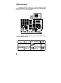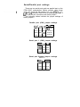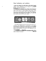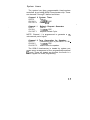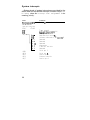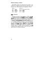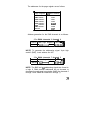
1
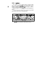
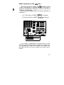
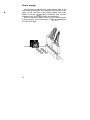
B.
PTM-7230C
12MHz Zero- Wait
Mini286 Mainboard
User Manual
Edition 1.05
0 1988 Datatech Enterprises Co., Ltd.
This manual and the Mini286 mainboard are copyrighted with all rights
reserved. Under the copyright laws neither this manual nor the Mini286
mainboard may be copied, in whole or in part, without the express
written consent of Datatech Enterprises Co., Ltd.
,
The following does not apply to any country where such provision s are
inconsistent with local law:
Datatech makes no warranties with respect to this documentation either express or implied and provides it “as is”. This includes but is not
limited to any implied warranties of merchantibility and fitness for a particular purpose. The information in this document is subject to change
without notice. Datatech assumes no responsibility for any errors that
may appear in this document. .
IBM and IBM PC/AT are registered trademarks of International Business
Machines Corp. VTI is a registered trademark of VLSI Technology Inc.
Intel is a registered trademark of Intel Corp. Landmark and Landmark
Speed Test are registered trademarks of Landmark Software. The
typeface used in the text of this manual is 12 point Helvetica and is
used under licence from the Allied Corporation, the owner of the
typeface.
Warnina
Reconfiguring
To ensure the reliability of the computer, N EVER
reconfigure the board while the power is ON.
If you wish to reconfigure the board at any time, ensure
that the power to the system is turned OFF before
changing any hardware settings such as DIP switches or
jumpers.
Note
1.
When you see an error message appears on the
screen after turning the power on, leave the system
switched on for one or two hours to recharge the
battery. You can then enter the system configuration.
2.
Leave your system switched on for 10 to 15 hours to
completely recharge the battery.
3.
If you had left the system switched off for more than
one month, follow step 2 above.
.
Contents
Introduction *.................................................................
1
Features. . . . . . . . . . . . . . . . . . . . . . . . . . . . . . . . . . . . . . . . . . . . . . . . . . . . . . . . . . . . . . . . . . . . . . . . . 2
Board layout . . . . . . . . . . . . . . . . . . . . . . . . . . . . . . . . . . . . . . . . . . . . . . . . . . . . . . . . . . . . . . . . 3
Installation .................................................................... 4-18
Location of jumpers ...................................................... 4
RAM installation ............................................................ 5
ROM installation ............................................................ 6
Serial/Parallel port settings ............................................ 7
Display adapter settings ................................................ 8
One-wait/zero-wait states .............................................. 8
Panel indicators and switches ....................................... 9
Math coprocessor installation ......................................... 13
Power supply connector ............................................... 14
Battery connector ......................................................... 17
.
Keyboard connector ................................................... .~18
Operation . . . . . . . . . . . . . . . . . . . . . . . . . . . . . . . . . . . . . . . . . . . . . . . . . . . . . . . . . . . . . . . . . . . . . . 19-22
Obtaining 12MHz Turbo mode . . . . . . . . . . . . . . . . . . . . . . . . . . . . . . . . . . . . . . 2. 0
Setting default operation mode . . . . . . . . . . . . . . . . . . . . . . . . . . . . . . ...*... 20
Software switch . . . . . . . . . . . . . . . . . . . . . . . . . . . . . . . . . . . . . . . . . . . . . . . . . . . . . . . . . . . . 20
Hardware switch . . . . . . . . . . . . . . . . . . . . . . . . . . . . . . . . . . . . . . . . . . . . . . . . . . . . . . . . . . . 2. 1
Alternate use of both switches . . . . . . . . . . . . . . . . . . . . . . . . . . . . . . . . . . . . . . 2. 2
.
Turbo LED and hardware switch . . . . . . . . . . . . . . . . . . . . . . . . . . . . . . . . . . . .22
One-wait/zero-wait option . . . . . . . . . . . . . . . . . . . . . . . . . . . . . . . . . . . . . . . . . . . . . .2 2
Technical information . . . . . . . . . . . . . . . . . . . . . . . . . . . . . . . . . . . . . . . . . . . . . 23-31
Microprocessor .............................................................
System timers ...............................................................
System interrupts .........................................................
ROM & RAM subsystems ..............................................
Direct memory access ...................................................
I/O channel slots ...........................................................
Math coprocessor .........................................................
Application note. . . . . . . . . . . . . . . . . . . . . . . . . . . . . . . . . . . . . . . . . . . . . . . . . . . . . . . . .
23
25
26
27
28
30
31
32
Introduction
The PTM4230C motherboard is compatible with the
PC/AT. This means that virtually all the software that is
available for the PC/AT can also be run on a system you
build around the PTM423OC motherboard.
Moreover, the same keyboard commands used on a
PC/AT can also be used on the PTM4230C motherboard.
For .example, the same <Ctrl> <AIt> <Del> combination of
keystrokes that is used for the software reset on the PC/AT
may also be used on your PTM-1230C-based system.
For this reason, the PTM4230C motherboard is the
ideal choice for a person seeking affordable AT-style
power.
The clear, well-illustrated instructions in this manual
ensure that even if you are a newcomer to the computer
world, you will have your system installed and running
with the minimum of effort.
Note:
Besure the jumper JPI is shorted when you install
your system.
Otherewise, you have to set up your system
configuration whenever you turn on your computer.
Features
802864 2 microprocessor (optional 80287 coproces-
sor)
Use’of VTI@‘s PC/AT compatible chip set.
Switchable between 8MHz Normal mode and 12MHz
Turbo mode by either a software switch or a hardware
switch.
8MHz I/O operation to keep compatibility with all
existing add-on cards.
8MHz Normal mode compatible with IBM PC/AT@ and
12MHz Turbo mode 195% faster than IBM PC/AT@Two serial ports and one parallel port onboard.
Onboard battery backup for CMOS configuration table
and real-time clock.
RAM subsystem of 512KB, 640KB or 1 MB.
RAM configurations of 640/384KB.
Eight expansion slots.
Sixteen-level interrupt.
Three-channel timer for music and time.
Seven-channel DMA for disk and special I/O.
32KB legal DTK BIOS@ (ADL certified) developed by
DATATECH ENTERPRISES CO., LTD.
Four-layer motherboard.
Speed test by Landmark@ Speed Test Program.
for one-wait state = 12MHz
for zero-wait state = 15.9MHz
2
Board lavout
The illustration below will familiarize you with the layout
of the PTM-1230C motherboard and its onboard ports:
r
Parallel Port
CN3
Installation
During the course of this section references will be
made to jumper settings, used to configure the various
functions of the PTM4230C mainboard. The following
diagram shows the locations of all the jumpers that may
need to be set.
J22
I
Jl
J3
J9
J2
J4
JIO
Location of jumpers
4
J5
Jll
RAM ins talla tion
Two jumpers, J8 and J9, are used to configure RAM
size on the motherboard. The two RAM banks can be
made to contain from 512KB, 640KB and up to 1 MB by
means of setting jumpers J8 and J9.
For the location of J8 and J9, refer to the illustration on
page 4.
To select the proper settings of the jumpers for the RAM
size that you want, refer to the table below:
J8
RAM type
J9
Short Short 512/O*
000000-07FFFF
Short Open1 640/O 1000000-09FFFd
Open Short 640/s&!
Open Ope
I
000000-09FFF
~OOOOO-~~FFF
nk0
256Kx 18
nkl
None
256Kx 181 64Kx18
256K X 18 256K X 18
Notallowed
* 512/O stands for 512KB base, OKB expansion memory
ROM installation
To install the ROM chips, refer to the illustration below
for the location of the chip sockets and the ROM selection
jumper, J22, on the motherboard:
.......
.. . .. .. . .. .. . .
la
I
-m
B-1
-m
m=
-------mm-
For selection and installation of the ROM BIOS chips,
refer to the table below:
Type of
BIOS
I
Other BIOS
of 32KB size I 27128 x 2 I
DTK BIOS
or any other
, of 64KB size
6
Type of
ROM configuration
ROM
chip I
I
I
27256 x 2
U56 - Low byte
U57- High byte
522
E0 0 l
U58 - Low byte
U57 - High byte
ml
Serial/Parallel port settings
There are two serial ports and one parallel port on the
PTM-1230C motherboard. Before actually using these
ports, you should set the jumpers J13, J14, J15, J16, J17,
J18 and J19 correctly. Refer to the illustrations on pages 3
& 4 to find the port connectors and these jumpers.
The following tables indicate the proper settings of
these jumpers:
Parallel port (CN3) jumper settings
CN31513( Jl41
J19
LPTI short short
ml short
1 2
LPT2 open open m2 3 l short
irrelevant
disable open short
irrelevant
disable short open
Serial port 1 (CN2) jumper settings
CN2 IJ15
J16
COMI short short
COM3 open open
disable open short
disable short open
Serial port 2 (CNI) jumper settings
CNl IJ17 1 J 1 8
COW short short
COM4 open open
disable open short
disable short open
Display adapter settings
Jumper Jll is used to select the display adapter. To
find jumper Jll on the motherboard, refer to the illustration on page 4.
To configure the motherboard for the kind of display
adapter you want, set jumper Jll according to the table
below:
Primary display attached to
monochrome display
Primary display attached to color
graphics monitor adapter
One-wait/zero wait states
Jumper J6 is used to select the zero-wait and one-wait
states. To find the jumper, refer to the illustration on page
4. The appropriate settings are shown below:
One-wait state operation
Zero-wait state operation
Panel indicators and switches
How you attach the mainboard to the case of your
system unit is largely up to you. This is because the PTM1230C Turbo mainboard can be used in a variety of
802864ype system unit cases.
Under typical conditions, your system unit will have all
the indicators and switches shown below and preferably
even a reset switch, a Turbo hardware switch and a Turbo
LED. If not, you can either install a new panel display or
omit some of these items from your system. Your computer
dealer offers an accessory which allows you to add the
two switches and the LED to your system.
The cables leading from this control panel will be connected to the appropriate pin connectors on the mainboard. Before you attach the mainboard to the case, you
should connect these cables to the mainboard. The locations on the mainboard are given in the diagrams on the
following pages.
The pinouts for the keylock pin connector,Ji, are given
in the following table. Refer to it to connect the keylock
cable to the pin connector.
Pin
Assignments
1
LED power
2
Not used
3
Ground
4
Keyboard in hibit
5
Ground
Note that pin 2 is not used and therefore the corresponding socket in the cable connector has no wire lead.
The wire for pin 1 can thus easily be identified and the
cable connector oriented correctly.
Functions of panel indicators and switches
Now that you have connected the panel indicators and
switches, you should understand something about their
functions:
l
l
Keylock The keylock is used to enable or disable the
keyboard. By disabling the keyboard, the user ensures
that anyone who does not have a key will be unable to
use the computer. U’nlocking the keylock enables the
keyboard. The keylock connector is located at Jl as
previously noted.
Power LED The power LED indicates whether the
power is on.
10
l
l
l
l
Hardware reset The reset switch restarts the computer from the RAM test stage. If you encounter any
problems while using unfamiliar software, you can always restart from the beginning by pressing the restart
button. The reset connector is jumper J2.
Turbo LED The Turbo LED indicates operation in
Turbo mode. The Turbo LED connector is jumper J4.
Turbo switch The Turbo switch changes operation
mode between Turbo and Normal. The Turbo switch
connector is jumper J5.
Speaker The speaker connector is located at J3.
The pinouts for the various switch and indicator
connectors are given on the following page.
11
Turbo LED jumper 54 pinouts
1
Select pin
2
Ground
Speaker jumper J3 pinouts
Pin
1
Function
q
Data out
2
5 VDC
3
Ground
4
5 VDC
Turbo hardware jumper J5 pinouts
Pin
Function
I
,
12
1
2
Select pin
1
Ground
\
Math coprocessor ins talla tion
D:
The math coprocessor located at U45 is optional. When
a 80287 coprocessor is installed the BIOS will check its
presence automatically. Setting any switch to indicate its
presence is unnecessary.
But choosing a proper 80287 for correct operation is
necessary:
l
For Turbo mode, an 80287-8 (8MHz) is required.
l
For Normal mode, an 80287-6 (6MHz) is required.
Coprocessor
Socket U45
If you install a coprocessor, be certain that it is the
correct one for the clock speed in which you intend to do
your processing. Consult the vendor from whom you
purchase the chip if you are in doubt as to which one to
choose.
13
Power supply
.
The final step is attaching the power supply cable to the
mainboard at connector J21. Looking from the top of the
case, on the left side of the power supply are some
cables. Find the 12-pin plastic connector (the four-pin
connectors are for the disk drives and hard disks).
Refer to the picture below. Pins 1 and 12 are numbered
in the picture for your convenience. The pinout description
is on the next page.
14
Assignments
Pin
.I
1
Power good
2
+5 VDC
3
+I
4
-12 VDC
5
Ground
6
Ground
7
Ground
a
Ground
9
-5VDC
10
+5 VDC
11
+5 VDC
12
+5 VDC
2 VDC
15
Choosing a power supply
The power supply provides a “power-good” signal to
indicate proper operation of the power supply. The powergood signal is a TTL-compatible high level for normal operation or a low level for fault conditions. If the powergood signal works well, then the system will function
properly. Otherwise, the data setting in CMOS RAM will be
lost. The following list gives you some guidelines for
choosing the right power supply:
l
l
The power-good signal should have a turn-on delay of
at least 200ms, but no longer than 5OOms when the
power is on (This means that the power-good signal
goes to a high level later than +W).
The power-good signal goes to a low level at least
1OOms before +5V falls below the regulation limits
when the power is off.
16
Battery connector
Finally, there is battery connector J12. This is for
connecting four size “AA” batteries instead of the circular
lithium battery (next to J12) to the CMOS RAM. For its
location, refer to the illustrations on page 4.
The battery connector pin assignments are as follows:
Pin
Assignments
Ground
Not used
Not used
6 VDC
17
Keyboard connector
Having fastened the mothervoard to the case, it only
remains to attach the keyboard. The keyboard connector
is located at the back of your system unit. Refer to the
illustration below:
Location of keyboard connector
from back panel
The pin assignments for keyboard connector J20 are as
follows:
Pin
Assignments
1
Keyboard clock
2
Keyboard data
3
Spare
4
Ground
5
+5 VDC
You have now finished configuring and connecting the
m inboard.
l!?
Battery connector
Finally, there is battery connector J12. This is for
connecting four size “AA” batteries instead of the circular
lithium battery (next to J12) to the CMOS RAM. For its
location, refer to the illustrations on page 4.
The battery connector pin assignments are as follows:
Pin
Assignments
Ground
Not used
Not used
6 VDC
17
Keyboard connector
Having fastened the mothervoard to the case, it only
remains to attach the keyboard. The keyboard connector
is located at the back of your system unit. Refer to the
illustration below:
Location of keyboard connector
from back panel
The pin assignments for keyboard connector J20 are as
follows:
Pin
Assignments
1
Keyboard clock
2
Keyboard data
3
Spare
4
Ground
5
+5 VDC
You have now finished configuring and connecting the
m inboard.
lf
Operation
The main advantage of the PTM4230C 12MHz zerowait mini-80286 Turbo mainboard over ordinary PC/AT
mainboards is its dual clock system. This innovation
makes it possible for your computer to operate at either of
two clock speeds: 8MHz or 12MHz. In the 12MHz Turbo
mode, your computer will operate up to 195% faster than
a conventional 80286.based computer.
Another special feature of the PTM-1230C mainboard
is the zero-wait/one-wait option in the Turbo mode. In zero
wait, your system will be around 195% faster than a IBM
PC/AT@ computer. In one-wait state, operation will be
around 80% faster.
Mode
DRAM used 1
Test Value
8 MHz/l wait
150 ns
8 MHz
8 MHz/O wait
120 ns
10.3 MHz
12MHzll wait
120 ns
12 MHz
12 MHz/O wait
80 ns
15.9 MHz
I
I
*Testing by Landmark Speed Test Program
To select the Normal/Turbo and one-wait/zero-wait
options, refer to the following instructions:
19
Obtaining 12MHz Turbo mode
.
This mainboard supports both a software switch and a
hardware switch for changes between Normal and Turbo
modes.
Setting default operation mode
The Turbo hardware switch, jumper J5 (shown on page
4), gives you the choice of running the PTM-1230C in
either Normal or Turbo mode when the power is on. For
default operation:
l
l
In Normal mode . . . . . Place a jumper cap over J5.
In Turbo mode . . . . . . . Take the jumper cap off J5.
Software switch
Before using the software switch, pay attention to
whether default operation is in Normal or Turbo mode. If it
is in Normal mode, do the following: press and hold down
the control < Ctrl > and alternate < Alt > keys on the keyboard while you press the minus < - > key. The cursor on
the screen will turn into a box. The Turbo LED on your
panel, if you have installed one, will light. For more
information on the Turbo LED, refer to the P a n e l
indicators and switches section. Now the computer is
in Turbo mode.
To return to Normal mode, press the same keys you
used to enter Turbo mode. When you enter Normal mode,
the cursor will return to the dash ( -) form and the Turbo
LED will turn off.
20
If default operation is in Turbo mode, press and hold
down the control c Ctrl > and alternate c Alt > keys on the
keyboard while you press the minus < - > key to go to
Normal mode. The Turbo LED will turn off, and the cursor
will turn into a box. To return to Turbo mode, press the
same keys: the Turbo LED will light and the cursor will
change into a dash.
Hardware switch
If you have a hardware switch on your panel, connect it
to jumper J5. More information on this is given in the
Panel indicators and switches section.
Push the hardware switch on to enter Normal mode,
and push it off to enter Turbo mode.
-
-
Hardware switch off
Hardware switch on
Using the hardware switch means that.the only indication of the mode your computer is in will be the Turbo
LED. It will turn on in the Turbo mode and turn off in the
Normal mode. The cursor will always have the same appearance.
21
Alternate use of both switches
Both the hardware and the software switches may be
used alternatively, but this is not advised because you
may become confused about the mode of operation.
When using both switches alternatively, the Turbo LED
will be the only accurate indicator of the actual mode: the
LED will be on in Turbo mode and off in Normal mode.
Turbo LED and hardware switch
Most 80286~type computer cases do not have a Turbo
LED or a Turbo hardware switch. However, both of these
items are very useful as you probably can already see.
Therefore, it is highly recommended that you install both
in your system if you do not already have them.
For more information, refer to Panel indicators and
switches section.
One- wait/zero- wait option
The one-wait/zero-wait option is selected by jumper J6
on the mainboard. Be aware that this option is only
available when the computer is in the Turbo mode. For
information on how to set the jumper, refer to 0 newait/zero wait states in the installation section.
22
Technical information
,Microprocessor
The 80286 is a high-performance microprocessor with
a 16-bit external data path, up to 16 megabytes of directly
addressable physical memory and up to one gigabyte of
virtual memory space. The operating speed of the 80286
chip is 8MHz in Normal mode and 12MHz in Turbo mode.
The 80286 operates in two modes: protected virtual
address and real address.
Virtual address mode
The virtual address mode provides a l-gigabyte virtual
address space mapped onto a 16 megabyte physical address space. Virtual address space is larger than physical
address space and the use of a virtual address that does
not map to a physical address location will cause a
restartable interrupt.
This mode uses 320bit pointers that consist of a 160bit
selector and offset components. The selector specifies an
index into a memory-resident table and the 24-bit base
address of the desired segment is obtained from the
memory table. A 16-bit offset is added to the segment
base address to form the physical address. The microprocessor automatically references the tables whenever’ a
segment register is loaded with a selector. Instructions
that load a segment register will refer to the memorybased tables without additional program support. The
memory-based tables contain 8-byte values called descriptors.
23
Real address mode
In this mode, physical memory is a contiguous array of
up to 1 megabyte. The selector portion of the pointer is
interpreted as the upper 16 bits of a 200bit address and
the remaining 4 bits are set to zero. This mode of operation is compatible with the 8088 and the 8086.
. Segments in this mode are 64KB in size and may be
read, written or executed. An interrupt may occur if data
operands or instructions attempt to wrap around the end
of a segment. In this mode, the information contained in
the segment does not use the full 64KB and the unused
end of the segment may be overlayed by another segment
to reduce physical memory requirements.
24
System timers
The system has three programmable timer/counters
controlled. by an Intel@ 8254-2 timer/counter chip. These
are channels 0 through 2 defined as follows:
Channel 0 System Timer
Tied on.
GATE 0
CLK IN 0
1 .lSOMHz OSC.
CLK OUT 0
8259A IRQ 0.
Channel 1
GATE 1
CLK IN 1
CLK OUT 1
Refresh Request Generator
Tied on.
1 .lSOMHz OSC.
Request Refresh Cycle.
NOTE: Channel 1 is programmed to generate a 15microsecond period signal.
Channel 2 Tone Generation for Speaker
GATE 2
Controlled by bit 0 of port hex 61 PPI bit .
1 .lSOMHz OSC.
CLK IN 2
Used to drive the speaker.
CLK OUT 2
The 8254-2 timer/counter is treated by system programs as an arrangement of four programmable external
I/O ports. Three are treated as counters; the fourth is a
control register for mode programming.
25
System interrupts
Sixteen levels of system interrupts are provided by the
80286 NMI and two 8259A Interrupt Controller chips. The
following shows the interrupt-level assignments in decreasing priority:
Level
Function
Microprocessor NMI
Parity or I/O channel check
Interrupt controllers
CTLR2
CTLR 1
IRQ 0
IRQ 1
IRQ 2
IRQ 8
IRQ 9
IRQ 10
IRQ 1 1
IRQ 12
IRQ 13
IRQ 14
IRQ 15
IRQ3
IRQ 4
IRQ 5
IRQ 6
IRQ 7
Timer output0
Keyboard(Outputbuffer full)
Interrupt from CTLR 2
Realtime clock interrup t
Software redirected to I NT OAH(IRQ 2)
Reserved
Reserved
Reserved
Coprocessor
Fixed disk controller
Reserved
Serial port 2
Serial port 1
Parallel port 2
Diskette controller
Parallel port 1
26
ROM subsystem
The ROM subsystem has a 32K by 16-bit arrangement
consisting of two 32K by 8-bit ROM/EPROM modules. The
odd and even address codes reside in separate modules.
The top of the first megabyte and the bottom of the last
megabyte address space is assigned to ROM (hex
OF0000 and hex FFOOOO). Parity checking is not done on
ROM.
DTK BIOS0 has been supported and placed in this
subsystem.
RAM subsystem
The RAM subsystem starts at address hex 000000. of
the 16M address space. It consists of either 640KB or 1 MB
of 256K or 64K by l-bit RAM modules. Memory refresh
forces one memory cycle every 15 microseconds through
channel 1 of the timer/counter. The following functions are
performed by the RAM initialization program:
0
0
Write operation to any memory location.
Initialize channel 1 of the timer/counter to the rate
generation mode (15 microseconds).
NOTE: The memory can be used only after being
accessed or refreshed eight times.
27
Direct memory access
Eight DMA channels are supported by the system. Two
Intel@ 8237-5 DMA controller chips (four channels in each
chip) are used. DMA channels are assigned as follows:
CTLR 1
Ch 0 -- Spare
Ch 1 -- SDLC
Ch 2 -- Diskette
Ch 3 -- Spare
CTLR 2
Ch 4 -- Cascade for CTRL 1
Ch 5 -- Spare
Ch 6 -- Spare
Ch 7 -- Spare
DMA channels
Channels 0 through 3 are contained in DMA control ler
1. Transfers of 8-bit data, g-bit I/O adapters and 8-bit or
16-bit system memory are supported by these channels.
Each of these channels will transfer data in 64KB blocks
throughout the 160megabyte system address space.
Channels 4 through 7 are contained in DMA controller
2. To cascade channels 0 through 3 to the microprocessor, use channel 4. Transfers of 160bit data between 16,bit
adapters and 160bit system memory are supported by
channels 5, 6 and 7. DMA channels 5 through 7 will
transfer data in 128KB blocks throughout the 16.
megabyte system address space. These channels will not
transfer data on odd-byte boundaries.
28
The addresses for the page register are as follows:
Page Register
DMA channel
DMA channel
DMA channel
DMA channel
DMA channel
DMA channel
DMA channel
Refresh
0
1
2
3
5
6
7
I/O Hex Address
0087
0083
0081
0082
0080
0089
008A
008F
Address generation for the DMA channels is as follows:
l
For DMA channels 3 throuah 0
1 Source 1 DMA Page Registers 1 8237A - 5 I
I Address I
A23H Al6
1 AlH-bAO 1
NOTE: To generate the addressing signal “byte high
enable” (BHE), invert address line AO.
l
For DMA channels 7 throuah 5
1 Source I DMA Page Registers I 8237A - 5 I
I
Address I
A23H Al7
1 A16tbAl 1
NOTE: The BHE and A0 addressing signals are forced to
a logic 0. DMA channel addresses do not increase or
decrease through page boundaries (64KB for channels 0
through 3 and 128KB for channels 5 through 7).
,2 9
l/O channel slots
The I/O channel supports:
l
l
l
l
l
l
l
l
Refresh of system memory from channel, microprocessors.
Selection of data accesses (either 8 bit or 16 bit).
Interrupts.
24-bit memory addresses (16MB).
I/O wait-state generation.
I/O address space hex 100 to hex 3FF.
Open-bus structure (allowing multiple.microprocessors
to share the system’s resources, including memory).
DMA channels.
Numbering of the I/O slots is as follows:
Jl-J8 I/O channels
GND
RESET DRV
+SVDC
IRQ9
-I/O CH CK
zz
%3
SD3
SD2
SD1
SD0
%;~
-’ 2i%
+ 12VDC
GND
-SMEMW
-SMEMR
I\;;
-D ACK3
DRQ3
so CH RDY
:Ki
SAW
8;s
a
SA12
-DE1
-RefrCel::
SAl 1
SAlO
:Eg
lRQ5
IRQ4
IRQ3
Ezi
SA7
SA6
SA5
-DAK
BALE
+5wg
GND
30
:z
.
.
zi:
SAO
JIO-J14 and J16 I/O channels
-MEM CS16
-I/O CS16
IRQlO
IRQll
IRQ12
IRQ15
IRQ14
-DACKO
DRQ0
-DACK5
DRQ5
-DACK6
DRQ6
-DACK7
“Dl
Cl+L
SBHE
LA23
LA22
LA21
LA20
LA19
LAW
LA17
-MEMR
-MEMW
SD08
SD09
SD1 0
SD1 1
SD1 2
SD1 3
SD1 4
SD1 5
Math coprocessor
The math coprocessor functions as an I/O device
through I/O port addresses hex 0F8, OFA and OFC. The
microprocessor sends OP codes and operands to I/O
ports. The microprocessor also receives and stores results
through the same I/O ports. The “busy” signal sent by the
coprocessor forces the microprocessor to wait until the
coprocessor is finished executing.
The following describes the math coprocessor controls:
OF0 The latched math coprocessor busy signal can be
cleared with an 8-bit “Out” command to port FO.
The coprocessor will latch “busy” if it asserts its
error signal. Data output should be zero.
0 Fl The math coprocessor will reset if an 8-bit “Out”
command is sent to port Fl. Again, the data
output should be zero.
31
Application note
The default operation mode depends on two things: the
hardware switch jumper setting as well as the type of keyboard controller (8042) used. The relationship between
them is described in the table below.
Default mode
Hardware switch
jumper
setting
I
I
Turbo
Open
Normal
S h o r t p[
Normal
Open
PI
DTK
’ (Mitsubishi Version)
lo]
1
Turbo
32
S h o r t m/
Type of 8042
DTK (Intel Version)
AMI
PHOENIX