1
FUJITSU Electronic Devices
User's Manual
2
F MC-16LX STARTER KIT
USER'S MANUAL
Revision History
Date
Jun 27, 2005
Description
Edition 1.0:
Initial release
© Fujitsu
Precautions
- The contents of this document are subject to change without notice.
- The general information of operation and samples of application circuits described in this
document are mere examples of standard operation and use of semiconductor devices.
not intended to guarantee the device operation in actual equipment.
They are
The customer who
incorporates the operation or sample circuit described in this document in the customer's system
should design the system on the customer's own responsibility.
Fujitsu will not assume
responsibility for damages resulting from the use of the information described in this document.
- The general information of operation, circuit diagrams, and other technical information described
in this document are not intended to grant the customer any license for the intellectual property
rights, such as patents and copyrights, and other rights held by Fujitsu or a third party.
Also, the
information is not intended to guarantee the customer to practice any intellectual property or other
rights held by third parties.
Fujitsu will not assume responsibility for infringement of any
intellectual property or other rights of third parties arising from the use of the information or
circuit diagrams.
- If any products described in this document represent goods or technologies subject to certain
restrictions on export under the Foreign Exchange and Foreign Trade Control Law of Japan, the
prior authorization by Japanese government according to the law is required for export of those
products from Japan.
Copyright© 2005 FUJITSU LIMITED All rights reserved
© Fujitsu
Contents
Preface........................................................................................................................................... 1
1
Setting Up of Starter Kit .............................................................................................. 2
1.1
Setting Up of Personal Computer ................................................................................ 8
1.1.1
Installing of USB driver ........................................................................................... 9
1.1.2
Installing of integrated development environment "SOFTUNE"
(limited-function version) ................................................................................... 10
1.1.3
Installing of demonstration version (trial version) of ACCEMIC MDE ................ 16
1.1.4
Setting up of evaluation board and connecting of board to the personal
computer.............................................................................................................. 21
1.1.5
Starting and setting up of SOFTUNE ..................................................................... 23
1.1.6
Starting and setting up of ACCEMIC MDE ........................................................... 26
1.1.7
Terminating of ACCEMIC MDE............................................................................ 37
1.1.8
Terminating of SOFTUNE ..................................................................................... 37
1.1.9
Board operation without ACCEMIC MDE ............................................................ 38
2
“Let's try to turn on the LED!”................................................................................... 40
2.1
What is an LED? ........................................................................................................ 40
2.2
How can the LED emit light? .................................................................................... 41
2.3
How to turn on an LED by microcomputer ............................................................... 42
2.4
How to create and execute a program to turn on the LED ......................................... 44
2.4.1
Outline of program to be created ............................................................................ 45
2.4.2
Creating and executing of program ........................................................................ 45
2.5
How to create and execute a program to make the LED blinking ............................. 46
2.5.1
Outline of the program to be created ...................................................................... 46
2.5.2
Creating and executing of program ........................................................................ 47
3
“Let's try to control the LED by switch operation!” .................................................. 49
3.1
How the microcomputer detects switch operation ..................................................... 49
3.2
How to create and execute a program to control LEDs by switch operation ............. 51
3.2.1
Outline of program to be created ............................................................................ 51
3.2.2
Creating and executing of program ........................................................................ 52
“Let's try to sound a buzzer!” .................................................................................. 54
4
4.1
Devices used for buzzer ............................................................................................. 54
© Fujitsu
4.1.1
Crystalline characteristics of piezoelectric device.................................................. 55
4.1.2
Piezoelectric characteristics.................................................................................... 55
4.1.3
Principle of piezoelectric device............................................................................. 56
4.2
Microcomputer and piezoelectric buzzer ................................................................... 56
4.2.1
Self-excited and separately excited vibrations........................................................ 57
4.2.2
Pulse wave generated by the microcomputer ......................................................... 57
4.3
How to sound the buzzer by PPG .............................................................................. 57
4.3.1
Setting of L-level and H-level duration .................................................................. 58
4.3.2
PPG count clock ..................................................................................................... 58
4.4
How to create and execute a program to sound the buzzer ........................................ 58
4.4.1
Outline of the program to be created ...................................................................... 59
4.4.2
Creating and executing of program ........................................................................ 60
4.4.3
Changing the tone of a buzzer sound...................................................................... 62
5
“Let's try to control the LED by interrupt.” ............................................................... 63
5.1
What is an interrupt? .................................................................................................. 63
5.2
How to detect a switch operation by interrupts.......................................................... 64
5.3
How to create and execute a program to control the LED by switch Input
operation ................................................................................................................. 65
5.3.1
Outline of the program to be created ...................................................................... 65
5.3.2
Creating and executing of program ........................................................................ 67
6
“Let's blink the LED by using a timer interrupt.” ...................................................... 69
6.1
What is a timer? ......................................................................................................... 69
6.2
How to create and execute a program to control the LED blinking by using a
timer interrupt ......................................................................................................... 70
6.2.1
Outline of the program to be created ...................................................................... 70
6.2.2
Creation and execution of the program................................................................... 72
7
“Let's use the A/D converter.”.................................................................................... 74
7.1
Analog and Digital..................................................................................................... 74
7.1.1
Outline of A/D converter ........................................................................................ 75
7.1.2
Scheme of volume tab ............................................................................................ 76
7.2
How to create and execute a program to display potental.......................................... 76
7.2.1
Outline of program to be created ............................................................................ 76
7.2.2
Creation and execution of the program................................................................... 80
8
“Let's use the temperature sensor.” ............................................................................ 82
8.1
What is a temperature sensor? ................................................................................... 82
8.2
How to detect temperatures by using "temperature sensor"....................................... 83
© Fujitsu
8.3
How to create and execute a program to display temperature ................................... 85
8.3.1
Outline of the program to be created ...................................................................... 85
8.3.2
Creation and execution of the program................................................................... 88
A
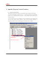
Appendix (Program Creation Procedure)................................................................... 90
A.1
Program Creation Procedure...................................................................................... 90
A.2
Program Building Procedure...................................................................................... 94
A.3
Program Execution Method ....................................................................................... 96
B
Appendix (Method To Write/Read Values in Registers) ............................................ 97
B.1
C
About the Method To Write/Read Values in Registers............................................... 97
Appendix (Method To Change the Include Path)....................................................... 98
C.1
About the Method To Change the Include Path ......................................................... 98
© Fujitsu
Preface
Thank you for your purchase of this Starter Kit.
The Starter Kit is intended for first-time users of microcomputers.
The Starter Kit is designed in
such a way that even beginners who have neither any actual experience with microcomputers nor
any knowledge about what microcomputers do and how they are used can easily learn about
microcomputers.
The Starter Kit includes a flash microcomputer and application development tools in order to
enable a user with some knowledge of C language to modify sample programs and make the
microcomputer actually perform various operations.
This User's Manual gives detailed
descriptions of how to control LED operations and buzzer sounds using the microcomputer.
Even users with no knowledge about programming languages will be able to comfortably learn in
an enjoyable way about microcomputers provided they have an introductory reference book on the
C language handy.
This User's Manual has been established incorporating various recommendations of employees
who had only been engaged in microcomputer-related work for one to three years and had had
only little prior knowledge of microcomputers to begin with.
Therefore, this User's Manual has
been written specifically for questions that beginners of microcomputers usually have.
The Starter Kit can be effectively used as a tool for training about electronic circuits or as
introductory education for embedded-software developers in classes at universities, technical
colleges, and industrial high schools, as well as in new-employee education programs at
corporations.
© Fujitsu
-1-
1 Setting Up of Starter Kit
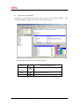
Before setting up the Starter Kit, make sure that all the components and equipment listed in Table
1.1 are ready for use.
You should install the software on your personal computer before connecting the evaluation board
to the personal computer.
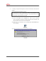
The Starter Kit software is available in two versions: A CD-ROM version and a download version
(the download version is not delivered on CD-ROM).
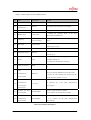
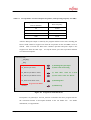
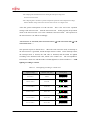
Table 1.1 List of components and necessary equipment
No.
1
Item
Board
Qty
1
Specification
Remarks
Evaluation board equipped with Fujitsu F2MC-16LX Series See Figure 1.1.
MB90F387 Microcomputer
2
USB cable
1
3
Installation
(1)
CD-ROM
USB
Accessory
CD-ROM for installing SOFTUNE, ACCEMIC MDE, and CD-ROM version
sample programs
only
Related manuals are contained on the CD-ROM.
The download
・User's Manual:
version has the
jouet_bleu_start_kit_manual_E.pdf
・USB Driver Installation Manual:
same contents.
USB_driver_installation_manual_E.pdf
・MB90385 Series Hardware Manual: MB90385_HM_E.pdf
・MB90385 Series Data Sheet:
MB90385_DS_E.pdf
・Set of SOFTUNE-related manuals:
SOFTUNE¥ MANUAL folder
4
Personal
computer
1
Personal computer on which Windows XP/Me/2000/98 can To be prepared by
operate normally
the user
USB2.0 port necessary
About 200 megabytes of free space necessary on the hard
disk
-2-
© Fujitsu
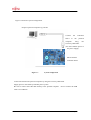
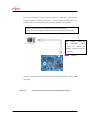
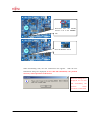
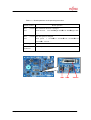
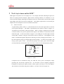
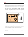
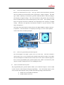
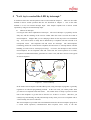
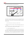
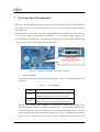
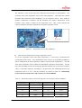
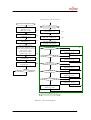
(2)Target device expansion pin(CN2)
(2) Target device expansion pin (CN1)
(1)Target device
(13) Oscillator for
main microcomputer
(10) USB host connecter
(5)LED
(12)
USB communication
microcomputer
expansion pin
(9)Buzzer
(3)Reset switch
(4)MODE switch
(6) Test switch
(8)Temperature
sensor
(7) A/D test VR
Figure 1.1
© Fujitsu
-3-
Board
(11)USB communication
microcomputer
(14) Oscillator for USB
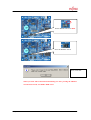
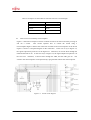
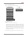
Figure 1.2 is a circuit diagram for the evaluation board.
Figure 1.2
Evaluation board circuit diagram
-4-
© Fujitsu
Table 1.2 lists the parts of the evaluation board.
No
Item
Specification
Function
(1)
Target device
MB90F387S
Main microcomputer (MB90F387S) on this board
26PINX2
I/O expansion pin of the main microcomputer
Pressing this switch resets the main microcomputer.
(2)
Target
device
expansion pin
(3)
Reset switch
A push switch
(4)
MODE switch
A slide switch
(5)
LED lamp
(6)
Test switch
2 push switches
(7)
A/D test VR
Slide VR
(8)
Temperature sensor
Thermistor
It
switches
the
operation
mode
of
the
main
microcomputer (MB90F387S).
5 LED lamps (1 red
LED lamps that are connected to the general-purpose
and 4 green lamps)
I/O pin
Push switches for tests that are connected to the
general-purpose I/O pin
A slide VR that is connected to the A/D converter input
A temperature sensor that is connected to the A/D
converter input
Kyocera's separate-excitation type piezo alarm with a
(9)
Buzzer
Buzzer
case (KBS-13DB-4P-2)
It is connected to the PPG timer output pin.
(10)
USB host connecter
A USB pin to connect the evaluation board and the host
MIN-B
PC
A USB communication microcomputer to connect the
USB
(11)
communication
main microcomputer (MB90F387S) and the host PC
MB90F334
It contains the USB communication firmware that has
microcomputer
been developed by Interface Co., Ltd.
USB
(12)
communication
microcomputer
An expansion pin of the USB communication
2 14-pins
microcomputer
expansion pin
(13)
Oscillator for main
microcomputer
Kyocera's crystal oscillator (CX-5FD)
CX-5FD (4MHz)
It is an oscillator for the main microcomputer.
Oscillator for USB
(14)
communication
Kyocera's crystal oscillator (CX-5FD)
CX-5FD(6MHz)
It is an oscillator for the USB communication
microcomputer
microcomputer.
Table 1.2 Evaluation board parts
© Fujitsu
-5-
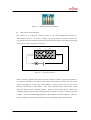
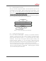
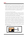
Figure 1.3shows the system configuration.
Prepare a personal computer by yourself.
Connect
board
the
to
computer
evaluation
the
personal
using
the
accessory USB cable.
(Use the USB bus power as
the power supply.)
Microcontroller
evaluation board
Figure 1.3
System configuration
Connect the board to the personal computer by using the accessory USB cable.
Supply power to the board by USB bus power system.
Be sure to connect the USB cable directly to the personal computer.
Do not connect the USB
cable via a USB hub.
-6-
© Fujitsu
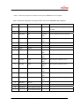
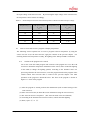
Table 1.3 shows the assignment of functions to the pins of MB90F387 microcomputer.
Table 1.3 Function assignments to the pins of F2MC-16LX Series MB90F387 Microcomputer
Pin-No.
3
Function
P50/AN0
Connection destination
VR
Logic
ANALOG
Remarks
Division of power supply voltage: 0
to 100%
4
P51/AN1
TEMP.SENSOR
ANALOG
1/2VCC@25°C
17
P25/INT5
SW1
Negative
L level when the switch is pressed
logic
19
P27/INT7
SW2
Negative
L level when the switch is pressed
logic
20
MD2
MODE
--
--
21
MD1
PULL-UP
--
--
22
MD0
MODE
--
--
23
RST
RESET
Negative
On when the output is L level
logic
29
P10/IN0
LED1
Negative
On when the output is L level
logic
30
P11/IN1
LED2
Negative
On when the output is L level
logic
31
P12/IN2
LED3
Negative
On when the output is L level
logic
32
P13/IN3
LED4
Negative
On when the output is L level
logic
33
P14/IN4
LED5
Negative
On when the output is L level
logic
36
P17/PPG3
BUZZER
Rectangular
Initially at L level, C coupling, bias R
wave
37
P40/SIN1
RS232C
--
--
39
P42/SOT1
RS232C
--
--
42
P30/SOT0
PULL-DOWN(50 kΩ)
--
--
43
P31/SCK0
PULL-DOWN(50 kΩ)
--
--
© Fujitsu
-7-
1.1
Setting Up of Personal Computer
This section describes how to install the software required to operate the Starter Kit on the
personal computer.
(Be sure to perform the software installation operation before connecting
the board to the personal computer.)
Take the following steps to set up the personal computer:
① Installing the USB driver (See the separately provided "USB Driver Installation
Manual.")
② Installing the integrated development environment "SOFTUNE" (limited-function
version) (See Item 1.1.2.)
③ Installing the demonstration version of ACCEMIC MDE (See Item 1.1.3.)
④ Connecting the evaluation board to the personal computer (See Item 1.1.4.)
⑤ Starting and setting up SOFTUNE (See Item 1.1.5.)
⑥ Starting and setting up ACCEMIC MDS (See Item 1.1.6.)
⑦ Terminating ACCEMIC MDE (See Item 1.1.7.)
⑧ Terminating SOFTUNE (See Item 1.1.8.)
-8-
© Fujitsu
1.1.1
Installing of USB driver
Install the USB driver according to the content of the "USB Driver Installation
Manual".
© Fujitsu
-9-
1.1.2
Installing of integrated development environment "SOFTUNE" (limited-function
version)
Install SOFTUNE (limited-function version).
The limited-function version of SOFTUNE is subject to the limitation on the
program size that can be debugged to 32 kilobytes.
The limited-function version
cannot be used to create a program over 32 kB.
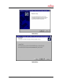
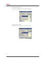
① Insert the CD-ROM into the CD-ROM drive.
When using the download
2
version, download the software for F MC-16LX Starter Kit (Jouet Bleu), and
open the folder where the files are decompressed.
② Double-click on the Setup.exe icon in the \\jouet_bleu \SOFTUNE folder to
start installation.
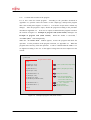
③ Follow the instructions on the screen to perform installation.
Click 'OK.'
-10-
© Fujitsu
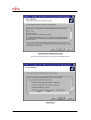
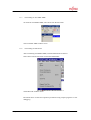
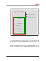
Click 'Next >.'
Click 'Next >.'
© Fujitsu
-11-
If you accept the agreement, click 'Yes.'
(If you refuse the agreement, you cannot install SOFTUNE.)
Click 'Next >.'
-12-
© Fujitsu
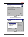
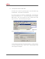
Click 'Next >.'
(Do not change the installation-destination folder here.)
Click 'Next >.'
© Fujitsu
-13-
Click 'Next >.'
The installation is executed.
-14-
© Fujitsu
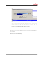
Click 'Finish.'
The installation of SOFTUNE (limited-function version) is completed.
Proceed to the installation of the demonstration version of ACCEMIC MDE.
© Fujitsu
-15-
1.1.3
Installing of demonstration version (trial version) of ACCEMIC MDE
Install the demonstration version (trial version) of ACCEMIC MDE.
The trial version of ACCEMIC MDE is subject to a limitation on the size of the
program that can be debugged to 12 kB. The trial version cannot be used to create
a program over 12 kB.
① Insert the CD-ROM into the CD-ROM drive.
When using the download
version, download the software for F2MC-16LX Starter Kit (jouet bleu), and
open the folder where the files are decompressed.
② Double-click the MDE_16LX_DEMO_V22ST_STARTERKIT.exe icon in the
\\jouet_bleu\MDE_16LX_DEMO_V22ST_STARTERKIT
folder
to
start
installation.
③ Follow the instructions on the screen to perform the installation.
Click 'Next >.'
-16-
© Fujitsu
If you accept the agreement, click 'Yes.'
(If you refuse the agreement, you cannot install ACCEMIC MDE.)
Click 'Next >.'
© Fujitsu
-17-
Click 'Next >.'
(Do not change the installation-destination folder here.)
Click 'Next >.'
-18-
© Fujitsu
Click 'Next >.'
The installation is executed.
© Fujitsu
-19-
When the installation is completed, click 'Finish >.'
Installation of the demonstration version of ACCEMIC MDE is completed.
Proceed to the setup of the evaluation board and its connection to the personal
computer.
-20-
© Fujitsu
1.1.4
Setting up of evaluation board and connecting of board to the personal computer
After the installation of SOFTUNE and ACCEMIC MDE, perform switch setting
on the evaluation board and connect the board to the personal computer.
On the evaluation board, set the MODE selector to PROG.
Set the MODE selector to
PROG.
MODE selector
PROG
Operation mode
Flash memory serial write mode
→ Used to write a program to the microcomputer
RUN
Single chip mode
→ Used to actually run the program written to the microcomputer
Confirm that the MODE selector is set to PROG.
Next, perform the cable connection.
© Fujitsu
-21-
Connect the USB port of the evaluation board to a USB port of the personal
computer using the accessory USB cable.
Do not connect the USB cable via a
USB hub, but connect it directly between the board and personal computer.
Connect the USB cable to a USB port of the personal computer.
For the location of USB port, refer to the manual for the personal computer.
After installing SOFTUNE
and
connect
ACCEMIC
the
board
MDE,
and
personal computer using the
USB cable.
USB port
The power of the evaluation board is supplied from the USB power supply (USB
bus power).
Figure 1.4
Connection of the evaluation board and personal computer
-22-
© Fujitsu
1.1.5
Starting and setting up of SOFTUNE
Preparation Before the operation described below, copy the sample programs to
the hard disk of the personal computer.
Uncompress the Fujitsu_starter_kit.zip file included in the CD-ROM
or among the downloaded files in an arbitrary directory.
Start SOFTUNE (limited-function version).
From the Start menu of Windows, select Programs (P) and Softune V3, in this order,
and then click on FFMC-16 Family Softune Workbench (trial version) to start.
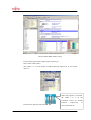
Open the workspace file for sample programs.
Select Open Workspace (R)... from the File (F) menu.
© Fujitsu
-23-
In this step, the workspace file to execute a sample program is opened.
(No
sample program is executed when the workspace file is opened.)
Open the Start_kit.wsp file located in the Fujitsu_starter_kit folder.
The project window displays the opened workspace.
-24-
© Fujitsu
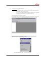
Make the settings for the active project.
Multiple projects can be stored in one workspace file.
The sample programs include already created projects, including LED.prj, Input.prj,
and Buzzer.prj.
Since program debugging is performed in units of projects, you should specify the
project to be debugged as an active project.
Select a project to be debugged and click the right mouse button.
A submenu appears.
Select Set active project from the submenu.
The project
name in the list is displayed in boldface, and debugging of the project is enabled.
© Fujitsu
-25-
1.1.6
Starting and setting up of ACCEMIC MDE
Use the Start_kit.wsp workspace file opened in the previous step to start ACCEMIC
MDE.
Confirm that the current active project of SOFTUNE is special.prj.
Select Build
(B) from the Project (P) menu to execute a build operation.
When the build operation is executed, the output screen of SOFTUNE displays the
messages below.
Build operation started...
--------------------Configuration: special.prj - Debug-------------------start905s.asm
monitor16LX.asm
_FFMC16.C
…
PPG_01_int.c
Linked...
*** I0312L: 0 warnings were output after S.C.F check.
D: ¥jouet_bleu¥fujitsu_starter_kit¥special¥Debug¥ABS¥apecial.abs
-----------------------------No error was found.
Confirm that no error was found.
------------------------------
-26-
© Fujitsu
If an error is detected as shown below in the build operation, perform the software
installation again from the initial step as described in Item 1.1.2.
When
reinstalling the software, be sure not to change the installation directory that is
displayed on the screen.
Build operation started...
-------------------- Configuration: special.prj - Debug-------------------start905s.asm
monitor16LX.asm
_FFMC16.C
*** D:¥jouet_bleu¥Fujitsu_start_kit¥special¥_ffmc16.c(9) E4038P: #include: File "_ffmc16.h" is
not found.
…
main.c
*** D:¥jouet_bleu¥Fujitsu_start_kit¥special¥main.c(17) E4038P: #include: File "_ffmc16.h" is not
found.
monitor16LX.asm
-----------------------------Error was found.
Example of error detection
------------------------------
© Fujitsu
-27-
Subsequently, ACCEMIC MDE starts automatically.
Input the COM port number that is confirmed after the USB driver is installed.
If you need to correct settings in the 'Select Processor dialog box' because you made
an incorrect "Type" setting or for other reasons, select 'Communication...' from the
Preferences menu to display the 'Select Processor dialog box.'
If the COM port number is unknown, use the following procedure to check the
COM port number to which the board is connected.
[Procedure for checking the COM port number]
First, click the right side of a mouse on the "My Computer", and click on
"Property(R)."
-28-
© Fujitsu
When the Property window of the system appears, click "Hardware," and then click
"Device manager (D)."
When the Device manager window appears, check the indication of "INTERFACE
USB to RS232C Converter Virtual COM Port(COMx)" under the "Port (COM and
LPT."
The "(COMx)" part indicates the COM port number.
[Note] If the assigned COM port number is 5 or higher, ACCEMIC MDE cannot be
used.
© Fujitsu
Change the PC settings so that 4 or lower number is assigned to the port.
-29-
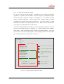
Click 'OK.' (With this trial version, the OK input will take effect 10 seconds later.)
Make the settings of the target microcomputer.
When you use ACCEMIC MDE for the first time, you should download the monitor
debugger kernel.
(You need not make these settings again unless you change the
target microcomputer.)
Here, select Fujitsu for "Manufacturer" and MB90F387 for "Type," and then click
'Next >.'
If you need to correct settings in the 'Select Processor dialog box' because you made
an incorrect "Type" setting or for other reasons, select 'Processor...' from the
Preferences menu to display the 'Select Processor dialog box.'
-30-
© Fujitsu
When the target microcomputer is the MB90F387, select FPT-48P-M26 for
"Package" and Not used for "PLL factor."
Do not change other parameters from
their defaults.
[Note]
Use either "Not used" or "1" for the PLL setting.
Note that the operations
are not guaranteed if any other value is entered.
After the setup, press "Download Kernel."
When ACCEMIC MDE is used for the first time, it is required to download the
monitor debugger kernel only once.
When the following information is displayed, reconfirm that the MODE selector is
set to the "PROG" side, press the RESET switch on the board, then press
"OK."
When you click OK after pressing the 'RESET' switch on the board, downloading
starts.
If the above switch operation is not performed in correct order, ACCEMIC
MDE will not start.
If you fail to perform switch operation correctly, resume
the operation from the step described in Item 1.1.6.
© Fujitsu
-31-
Reconfirm
that
the
MODE
selector is set to the "PROG"
side.
Press the 'RESET' switch.
When downloading ends, the next information item appears.
With the next
Information dialog box displayed, do not click OK immediately but perform
necessary switch operations on the board.
When this dialog box is
displayed, do not click
OK immediately, but
perform
switch
operations on the board.
-32-
© Fujitsu
Set the MODE selector to RUN.
Press the 'RESET' switch.
Now, click 'OK.'
When you click 'OK' in the Information dialog box after pressing the 'RESET'
switch on the board, ACCEMIC MDE starts.
© Fujitsu
-33-
The ACCEMIC MDE window opens.
Execute the program of the sample project "special.prj."
Select "Run" under "Start."
The LEDs 1 to 5 on the board are shifted leftward respectively at one-second
interval.
When the program is executed,
the LEDs 1 to 5 on the
evaluation board are shifted
leftward
It also has the functions listed in Table 1-4.
-34-
respectively
one-second interval.
© Fujitsu
at
Table 1-4 Board operations at the special.prj execution
Switch control
SW1
Board operation
normal The LED shift direction is changed.
press
Shift direction:
Left shift
Right shift
Left shift
Right shift-
---SW2
normal The shift speed is changed.
press
Shift speed:
seconds
1 second
0.5 seconds
0.25 seconds
0.125
1 seconds- - -
SW1 long press
It controls on and off of the buzzer.
Volume
It can adjust the volume of the buzzer while buzzer sounds.
adjustment
SW1
© Fujitsu
-35-
SW2
Volume
Stop the program as follows:
Select Stop from the Start menu to stop the sample program.
Reset the program as follows:
Select Restart from the Start menu.
-36-
The program is reset.
© Fujitsu
1.1.7
Terminating of ACCEMIC MDE
To terminate ACCEMIC MDE, select 'Exit' from the File menu.
The ACCEMIC MDE window closes.
1.1.8
Terminating of SOFTUNE
After terminating ACCEMIC MDE, terminate SOFTUNE as follows:
Select 'Exit' from the File menu to terminate SOFTUNE.
The SOFTUNE window closes.
Described above are the basic operation procedures using sample programs to start
debugging.
© Fujitsu
-37-
1.1.9
Board operation without ACCEMIC MDE
This Starter Kit can operate the generated program on the board without using
ACCEMIC MDE.
The procedure is described below.
First, start the program to be operated on ACCEMIC MDE.
The procedure for
operation is described in Item 1.1.6. Confirm that the program runs on ACCEMIC
MDE normally.
Then, stop the program, and select "Automatic Start" under
"Tools" in the menu.
Then, the following window appears.
Then, put a checkmark on "Automatic start after reset," and press "OK."
It starts erasing the Flash memory and writing the program.
of seconds to complete the writing.
Wait for a while.
It takes several tens
When the program writing
ends, the progress bar disappears.
-38-
© Fujitsu
After the writing ends, stop ACCEMIC MDE and SFTUNE.
Then, press the
"RESET" button on the board while the USB cable is connected.
The same
operations as confirmed on ACCEMIC MDE are available.
Described above are the basic operation procedures by using the sample programs to
start debugging.
Next, let's try to control LED lighting!
© Fujitsu
-39-
2 “Let's try to turn on the LED!”
LEDs appear everywhere in our everyday lives -- for example, the LEDs indicating the power-on
status of a laptop personal computer, digital camera, washing machine, air conditioner, or rice
cooker, the LEDs display indicating train departure times at a railroad station, and in traffic signals
using LEDs, which have now become widespread.
This chapter explains how to control the port
output of the microcomputer to turn on an LED on the board.
2.1
What is an LED?
A light-emitting diode (LED) is a semiconductor device that emits light when an electric
current passes through it. The LED is represented by the symbol as shown in Figure 2.1.
An LED has two electrodes: anode and cathode.
When a voltage is applied across the LED
so that the anode is at a positive potential with respect to the cathode, a current flows and the
LED emits light.
In the circuit shown in Figure 2.1, the LED goes on (emits light) when the
switch (SW) is turned on and goes off when the switch is turned off.
The brightness of the
LED is controlled through the adjustment of flowing current by changing the resistance.
the current becomes larger, the emitted light becomes brighter.
orange, yellow, green, or blue.
As
An LED can emit light in red,
Since the three primary colors (blue, green, and red) of light
can be produced by combinations of the five colors, a full-color can be displayed by LEDs.
Anode
LED
SW
Cathode
Figure 2.1
LED
Compared with an incandescent lamp, the LED has lower power consumption, longer
operating life, and shorter response time.
So, the LED is used in lighting equipment,
backlight for liquid-crystal display monitor, traffic signals, tail lamps of cars, and displays.
The board has red of LED3 and green of LEDs1, 2, 4, and 5 as shown in Figure 2.2.
-40-
© Fujitsu
LEDs mounted on the board
Figure 2.2
2.2
How can the LED emit light?
The LED has a pn-junction structure, which is the most fundamental structure of
semiconductor devices. As shown in Figure 2.3, the pn-junction structure consists of a
p-type semiconductor containing many electron holes and an n-type semiconductor containing
many electrons that are joined to each other.
n type
p type
+
+
+ electrode
+
+
+
+
-
-
-
-
+
-
-
+emission-
+
+
Light
-
- electrode
pn-junction surface
Figure 2.3
pn-junction structure
When a voltage is applied across the pn-junction structure so that the n-type semiconductor is
at a negative potential with respect to the p-type semiconductor, electrons move from the
n-type semiconductor to the p-type semiconductor , electron holes move in the reverse
direction, and thereby a current flows.
Then, some of electron holes and electrons collide
with each other and are combined together.
When an electron hole and an electron are
combined together, they lose their energy partially, and the lost energy is emitted in the form
of light.
The color of emitted light depends on the material of the semiconductor. Table 2.1
shows examples of semiconductor materials and corresponding colors of emitted light.
© Fujitsu
-41-
Table 2.1 Examples of semiconductor materials and colors of emitted light
2.3
Semiconductor material
Color of emitted light
ZnCdSe
Blue
ZnTeSe
Green
AlGaAs
Red
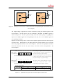
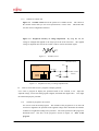
How to turn on an LED by microcomputer
Figure 2.1 showed an example of circuit in which an LED is turned on and off by turning on
and off a switch.
This section explains how to control the switch using a
microcomputer.Figure 2.4shows the connection of LEDs to the microcomputer on the board.
Figure 2.5 shows a conceptual diagram of the connection.
In the case of (a) in Figure 2.5,
the signal output from pin P10 is at the high level. Therefore, no current flows through the
LED and the LED is off. In the case of (b) in Figure 2.5, the signal output from pin P10 is at
the low level.
Therefore, a current flows through the LED, and the LED goes on. The
switch in the microcomputer can be operated by a program that controls the microcomputer.
Figure 2.4
Actual circuit diagram
-42-
© Fujitsu
Microcomputer
Microcomputer
LED
LED
On
Off
Pin P10
Pin P10
(a) LED is off.
(b) LED is on.
Figure 2.5 Example of circuit to turn on/off an LED (with a conceptual diagram of the internal circuit of
microcomputer)
The output settings of pins P10 to P14 are controlled by using the internal registers of the
microcomputer.
The pins P10 to P14 are controlled by the PDR1 and DDR1 registers as
shown in Figure 2.6.
To use a port for output, write the value (0 [low] or 1 [high]) to be
output to the PDR1 register bit corresponding to the pin, and 1 to the DDR1 register bit
corresponding to the pin.
Registers are the memory areas to control microcomputer operation and retain microcomputer
operation status.
Writing data to, and reading data from registers enables you to control the
CPU and peripheral functions of the microcomputer.
Here, the term peripheral functions
means the functions of the I-O ports, timers, and A/D converter incorporated in the
microcomputer.
bit
7
6
5
4
3
2
1
0
- For input setting, this register is used to check the input level
of each pin (value read from the bit corresponding to each
PDR1 register
pin: 0 [low-level input] or 1 [high-level input]).
(IO_PDR1.byte)
Pin name P17 P16 P15 P14 P13 P12 P11 P10
- For output setting, this register is used to set the output level
of each pin (value written to the bit corresponding to each
pin: 0 [low-level output] or 1 [high-level output]).
bit
7
6
5
4
3
2
1
0
DDR1 register
- This register is used to specify whether each port (pin) is
(IO_DDR1.byte)
used for input or output (value written to the bit
Pin name P17 P16 P15 P14 P13 P12 P11 P10
corresponding to each pin: 0 [input] or 1 [output]).
Example of P10 setting
Input setting (DDR1 bit0 = 0)
PDR1 bit0
When 0 is read
Low-level input
When 1 is read
High-level input
Figure 2.6
© Fujitsu
Output setting (DDR1 bit0 = 1)
When 0 is written
Low-level output
When 1 is written
High-level output
Explanation of registers to control the output from P10 to P14
-43-
The internal switch of microcomputer as shown in Figure 2.5 actually consists of a p-channel
type transistor and an n-channel type transistor as shown in Figure 2.7.
The pin outputs a
low-level signal when the n-channel type transistor is in the on state; the pin outputs a
high-level signal when the p-channel type transistor is in the on state.
You can switch the
output level of each port by setting the relevant value in the PDR1 register of the
microcomputer.
In the example shown in Figure 2.7, '0' is written to the bit 0 of PDR1to set
pin P10 for low-level output, and '1' is written to the bit 1 of PDR1 to set pin P11 for
high-level output.
With these settings, LED0 is turned on, and LED1 is turned off.
Microcomputer
LED0
On
Input DDR1 bit0=1
0
PDR1 bit0=0
Output 1
Pin P10
n-channel type
transistor ON
PDR1 bit1=1
Input
p-channel type
transistor ON
DDR1 bit1=1
LED1
0
Off
1
Pin P11
Output
Figure 2.7
LED on/off control by rewriting the PDR1 register (with a conceptual diagram of the
internal circuit of microcomputer)
On the board, the LEDs are connected to pins P10 to P14.
the output mode for controlling the LEDs.
Therefore, the five pins are set to
When the microcomputer is reset, all bits of DDR
are reset to 0 (initial value), which means the ports are set to the input mode. In this status,
to use a pin as an output port, be sure to write '1' to the bit corresponding to the pin.
2.4
How to create and execute a program to turn on the LED
This section explain how to create a program that actually controls a microcomputer pin to
turn on an LED.
-44-
© Fujitsu
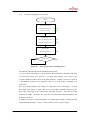
2.4.1
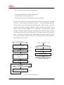
Outline of program to be created
Here, you will create a program that outputs a low-level signal from pin P14 of the
microcomputer to turn on LED5.
Figure 2.8 shows the flow of the program.
In the
flow, a value is set in the PDR1 register first, and then output setting is made using the
DDR1 register.
For port output, be sure to set the output level in the PDR1 register
before the output setting using the DDR1 register.
The setting operation should be
performed in this order because the initial value that is applied after the microcomputer is
reset is not defined for the PDR1 register (to set the output level).
START
Set LED5 to on.
Set P14 output level to low (PDR1.bit4=0).
(1)
Set P14 to output mode
(DDR1.bit4=1)
(2)
Infinite loop
Figure 2.8
2.4.2
(3)
Flow of the program to turn on the LED
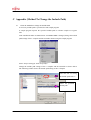
Creating and executing of program
Let us now create the actual program.
According to the procedure described in
Appendix A.1, open the source file "main.c" stored in ”sample.prj”, and input the program
portion enclosed by dotted line in Figure 2.9.
modification.
Use the files other than "main.c" without
After the input of the program, build the program according to the
procedure described in Appendix A.2.
If an error message is output, check that the
content of the input program is exactly the same as the description shown in Figure 2.9.
When the build operation ends successfully, ACCEMIC MDE starts automatically.
After the ACCEMIC MDE window appears, execute the program and check its operation.
For how to execute the program, see Appendix B.1.
you can see that LED5 goes on on the board.
© Fujitsu
-45-
While the program is executed,
void main(void)
{
IO_PDR1.byte=0xEF;
(1) LED5 on setting (P14=Low, P10 to P13=High)
IO_DDR1.byte=0x1F;
(2) P10 to P14 output setting
while(1);
(3) Infinite loop
}
Program to be added
Figure 2.9
Program to turn on the LED
Descriptions ”IO_XXX.byte” and ”IO_YYY.bit” included in the above program code are
the convenient formats of description defined in the I-O header file.
For further
information, see Appendix B.1.
2.5
How to create and execute a program to make the LED blinking
This section explains how to create a program that makes the LED be blinking.
2.5.1
Outline of the program to be created
Here, you will create a program that switches the output from pin P14 of the
microcomputer between the low and high levels repeatedly to make LED5 turn on and
off repeatedly.
While 0 and 1 are written alternately to the bit 4 of the PDR1 register ,
LED5 is blinking as shown below.
On
Off
LED5 is on. (LED1 to LED4 are off.)
Figure 2.10 shows the flow of the program.
LED5 is off. (LED1 to LED4 are off)
The only difference of this program from
the LED lighting program shown in Figure 2.8 is that this program has additional steps
of LED off and LED on/off time count processing.
The LED on/off time count
processing is described by the for-statement as shown below to enable you to visually
confirm the on/off operation of the LED.
You can vary the on/off time by changing
the currently set value (30000).
- On/off time count
for(i=0;i<30000;i++);
-46-
© Fujitsu
START
Set LED5 to on.
Set P14 output level to low (PDR1.bit4=0).
(1)
Set P14 to output mode
(DDR1.bit4=1)
(2)
no
Count reached 30000?
(3)
yes
Set LED5 to off.
Set P14 output level to high (PDR1.bit4=1).
(4)
no
Count reached 30000?
(5)
yes
Set LED5 to on.
Set P14 output level to low (PDR1.bit4=0).
Figure 2.10
2.5.2
(6)
Flow of the program to make LED5 blinking
Creating and executing of program
Let us now create the actual program.
According to the procedure described in
Appendix A.1, open the source file "main.c" stored in ”sample.prj”, and input the program
portion (after "while (1)") enclosed by dotted line in Figure 2.11 to the LED lighting
program created in Section 2.4.2.
Use the files other than "main.c" without modification.
After the input of the program, build the program according to the procedure described in
Appendix A.2.
If an error message is output, check that the content of the input program
is exactly the same as the description shown in Figure 2.11. When the build operation
ends successfully, ACCEMIC MDE starts automatically.
After the ACCEMIC MDE window appears, execute the program and check its operation.
For how to execute the program, see Appendix A.3.
can see that LED5 goes on on the board.
© Fujitsu
-47-
While the program is executed, you
void main(void)
{
IO_PDR1.byte=0xEF;
(1) LED5 on setting (P14=Low, P10 to P13 =High)
IO_DDR1.byte=0x1F;
while(1)
{
}
}
(2) P10 to P14 output setting
int i;
for(i=0;i<30000;i++);
(3) LED5 on time count
IO_PDR1.byte=0xFF;
(4) LED5 off setting (P10 to P14 =High)
for(i=0;i<30000;i++);
(5) LED5 off time count
IO_PDR1.byte=0xEF;
(6) LED5 on setting (P14=Low, P10 to P13=High)
Program to be added
Figure 2.11
Program to make LED5 blinking
-48-
© Fujitsu
3 “Let's try to control the LED by switch operation!”
This chapter explains how to control LEDs by operating the push switches on the board and how
to create a program that controls LEDs based on switch operations.
3.1
How the microcomputer detects switch operation
The board of the Starter Kit has two switches (SWs) as shown in Figure 3.1.
are connected to pins P25 and P27 of the microcomputer.
The switches
The following explains how the
microcomputer detects your operation of these switches.
SW1
Figure 3.1
SW2
Switches on the Starter Kit board
Figure 3.2 shows a conceptual diagram of the connection of SW1 on the board.
On the board,
SW1 is connected to pin P25, which is a general I-O port of the microcomputer. While SW1
is released (off state), the voltage applied to pin P25 of the microcomputer is Vcc (5 V), which
is the high-level input.
When SW1 is pressed (on state), the input to pin P25 becomes the
low level because the voltage at pin P25 becomes GND.
Thus, the input status at pin P25 of
the microcomputer changes depending on the state of SW1.
The same mechanism applies to
SW2, except that SW2 is connected to pin P27, which is a general I-O port of the
microcomputer.
Therefore, the input status at pin P27 changes when SW2 is operated.
■When SW1 is off
■When SW1 is on
Vcc
Microcomputer
Vcc
Microcomputer
Pin P25
Pin P25
SW1
PDR2 register
Figure 3.2
© Fujitsu
SW1
PDR2 register
GND
GND
Connection of SW1 to microcomputer pin (conceptual diagram)
-49-
The change of pin status can be detected by a program running on the microcomputer
The
microcomputer of the Starter Kit can determine the status of pins P25 and P27 from the
corresponding values in an I-O port register (PDR2).
instructions of a microcomputer program.
Register values can be read using
In other words, the microcomputer can determine
the operation state of a switch by reading the corresponding value from PDR2 by the program.
Let us explain some specifications of PDR2.
status of port 2 pins (P20 to P27).
the bits of PDR2.
PDR2 is the 8-bit register that indicates the
Figure 3.3 shows the association of the pins at port 2 with
When a pin is at the high level, the corresponding bit is 1; when the pin is
at the low level, the bit is 0.
Therefore, the status of pin P25, or the operation state of SW1,
can be known when the value of the bit 5 of PDR2 is read.
Similarly, the operation state of
SW2 can be known when the bit 7 of PDR2 is read.
Inside of
Bit
0
1
2
3
4
5
6
7
0
1
2
3
4
5
6
7
DDR2
Bit
PDR2
Port 2 pins
P20 P21 P22 P23 P24
P26
P25
Figure 3.3
P27
*PDR value
High : 1, Low : 0
SW2
SW1
Outline of PDR2 and DDR2 registers (conceptual diagram)
When using port 2 pins, you must specify whether they are used for input or they are used for
output.
DDR2 is the 8-bit register to switch the signal direction (between input and output)
of each pin at port 2. The association of the bits of DDR2 with the pins at port 2 is as shown in
Figure 3.3. To use a pin for output, 1 should be written to the corresponding bit of DDR2; to
use the pin for input, 0 should be written to the corresponding bit of DDR2.
Here, P25 and
P27 are used as input pins to input signals from SW1 and SW2. Therefore, 0 should be
written to the bits 5 and 7 of DDR2.
The above explanation can be summarized into the following processes to detect the switch
state by a microcomputer program:
(1) Write '0' to DDR2 bits 5 and 7, and set port 2 pins P25 and P27 to input mode.
(2) Read the values of PDR2 bits 5 and 7.
-50-
© Fujitsu
- When the read value is '0,' the switch can be determined to be in the on state.
- When the read value is '1,' the switch can be determined to be in the off state.
3.2
How to create and execute a program to control LEDs by switch operation
This section explains how to create a program to detect the switch operation state.
The
program also controls LED operation to enable you to visually know that the switch operation
state is detected.
The program applies the method of turning on the LED described in the
previous chapter.
3.2.1
Outline of program to be created
The operation of the program to be created is as described below.
Figure 3.4 is the flow
of the program that performs the operation.
(1) When SW1 is pressed, LED1 is turned on.
(2) While SW1 is in the on state, LED1 is kept lighting.
(3) When SW1 is released (set to off), LED1 is turned off.
(4) Similarly, LED2 is turned on and off according to the SW2 state.
START
Set output pins for LED1 and LED2
(PDR1.bit0=1, PDR1.bit1=1)
-------------
Set input pins for SW1 and SW2
(DDR2.bit5=0, DDR2.bit7=0)
(1)
------------- (2)
(3)
SW1 input state?
PDR2.bit5 = 1
PDR2.bit5 = 0
(4)
Set LED1 to off (PDR1.bit0 = 1)
Set LED1 to on (PDR1.bit0 = 0)
(6)
SW2 input state?
(5)
PDR2.bit7 = 1
PDR2.bit7 = 0
(7)
Set LED2 to on (PDR1.bit1 = 0)
Figure 3.4
© Fujitsu
(8)
Set LED2 to off (PDR1.bit1 = 1)
Flow of program
-51-
This program first sets the output pins for the LEDs, and then sets the input pins for the
switches.
The necessity of these settings was explained in the previous section.
The
program subsequently reads the value of the bit 5 of PDR2 to detect the state of SW1.
The program turns on or off LED1 according to the read value.
To turn on and off
LED1, the program writes 0 or 1, respectively, to the bit 0 of PDR1. Also for SW2, the
program performs the similar processing and controls LED2.
3.2.2
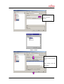
Creating and executing of program
Let us now create the actual program.
According to the procedure described in
Appendix A.1, open the source file "main.c" stored in ”sample.prj”, and input the program
portion enclosed by dotted line in Figure 3.5.
modification.
Use the files other than "main.c" without
After the input of the program, build the program according to the
procedure described in Appendix A.2.
If an error message is output, check that the
content of the input program is exactly the same as the description shown in Figure 3.5.
When the build operation ends successfully, ACCEMIC MDE starts automatically.
After the ACCEMIC MDE window appears, execute the program and check its operation.
For how to execute the program, see Appendix A.3.
SW1 or SW2.
After executing the program, press
If LED1 or LED2 goes on, the program operation is correct.
void main(void)
{
__set_il(7);
__EI();
IO_PDR1.byte = 0x00;
IO_DDR1.byte = 0x1F;
(1) Port 1(LED control) output setting
IO_DDR2.byte = 0x00;
(2) Port 2 (SW input) input setting
while(1)
{
if(IO_PDR2.bit.P25==1){
IO_PDR1.bit.P10 = 1;
}
else{
IO_PDR1.bit.P10 = 0;
}
if(IO_PDR2.bit.P25==1){
IO_PDR1.bit.P10 = 1;
}
else{
IO_PDR1.bit.P10 = 0;
}
(3) SW1 input state?
(4) LED1 on
(5) LED1 off
(6) SW2 input state?
(7) LED2 on
(8) LED2 off
}
Program code added
}
Figure 3.5
Sample program code (main routine)
-52-
© Fujitsu
Descriptions ”IO_XXX.byte” and ”IO_YYY.bit” included in the above program code are
the convenient formats of description defined in the I-O header file.
information, see Appendix B.1.
© Fujitsu
-53-
For further
4 “Let's try to sound a buzzer!”
Our daily life is full of sounds. Many of them are not natural sounds but artificial sounds that
give us signals, draw our attention to something, and give us information.
The loud sound of the
alarm clock wakes us up every morning. The cooking timer buzzer sounds to let us know when
to stop boiling eggs for our favorite softness of yolk.
We are surrounded and given much
information by artificial sounds varied in loudness and tone, including those of microwave ovens,
level crossing alarms, and automobile horns.
Microcomputers are often used to produce these artificial sounds.
to control the timing, tone, and pitch of a sound.
A microcomputer can be used
This chapter explains how to control a buzzer
sound simply by using microcomputer functions.
4.1
Devices used for buzzer
Before explaining the mechanism of a buzzer, this section describes the piezoelectric device
that is used for a buzzer.
A piezoelectric device is a circuit element that uses a piezoelectric effect.
The piezoelectric
device incorporates a substance characterized by the piezoelectric effect (which causes a
voltage when an impact or pressure is applied) or the inverse piezoelectric effect (which
causes a crystalline distortion when a voltage is applied).
A quartz oscillator is a familiar example of piezoelectric device that uses the piezoelectric
characteristics.
The buzzer to be controlled by the microcomputer of the Starter Kit
incorporates this piezoelectric device. Piezoelectric devices are also used for piezoelectric
loudspeakers, crystal earphones, vibration sensors, and microphones.
-54-
© Fujitsu
4.1.1
Crystalline characteristics of piezoelectric device
A piezoelectric device uses a substance that has a polarization characteristic.
Some crystals have an electrical deflection as an inherent characteristic.
This
characteristic is called "polarization," and the crystal having this characteristic is called a
"polarized crystal."
More specifically, the polarized crystal contains polarized molecules
as shown in Figure 4.1.
In the figure, the direction of polarization is represented by the green arrow indicating the
direction from the positive (+) pole to the negative (-) pole.
+
ー
+
ー
+
ー
+
ー
+
ー
+
ー
+
ー
+
ー
+
ー
+
ー
Figure 4.1
4.1.2
Polarization of molecules and crystal
Piezoelectric characteristics
As shown in Figure 4.2, a crystal sometimes has a characteristic that expands the crystal
when a voltage is applied in the direction of polarization (direction of green arrow).
characteristic is called the piezoelectric effect.
This
When a piezoelectric crystal is given a
voltage in the reverse direction of polarization (reverse direction of green arrow), the
crystal contracts.
++++++++++
---------------------------
++++++++++++++++
------------------
Expansion
Contraction
Figure 4.2 Piezoelectric crystal
© Fujitsu
-55-
4.1.3
Principle of piezoelectric device
When an AC voltage is applied across a piezoelectric crystal, the crystal contracts or
expands alternately each time the direction of current is reversed as shown in Figure 4.3.
The cycle of contraction and expansion changes when the frequency of AC voltage is
varied. This characteristic can be used to vibrate the crystal at various frequencies. If
the vibrational energy of the crystal is large, the crystal can generate an aerial vibration,
which makes a sound. Piezoelectric buzzers use this principle.
++++++++++
---------------------------
++++++++++++++++
------------------
Contraction
Expansion
Figure 4.3 Principle of piezoelectric device
4.2
Microcomputer and piezoelectric buzzer
A piezoelectric buzzer uses a piezoelectric device as described above. To produce a sound
from the piezoelectric buzzer, you should apply a changing voltage, e.g., AC or pulse voltage,
to the buzzer. Here, let's sound a piezoelectric buzzer by using a pulse wave (pulse voltage)
output from the microcomputer.
Pulse input
Vibration
Figure 4.4
Buzzer using a piezoelectric device
-56-
© Fujitsu
4.2.1
Self-excited and separately excited vibrations
Buzzers are classified into two types. One type, called a self-excited buzzer, generates
only one sound by the self-resonance of the crystal when a voltage is applied. The other
type, called a separately excited buzzer, generates different kinds of sound according to
the frequency of applied voltage. The self-excited buzzer can generate only one kind of
buzzer sound based on the self-resonant frequency of the crystal. The separately excited
buzzer can generate the buzzer sound that varies depending on the frequency of applied
voltage. Therefore, the separately excited buzzer enables to vary the sound in a wide
range of frequencies.
The board of the Starter Kit has a built-in buzzer, the KBS-13BB-4P-2 made by Kyocera
Corporation. Since this buzzer is of separately excited type, it can be used to produce
various tone colors of sound in principle.
buzzer
Figure 4.5
4.2.2
buzzer
Pulse wave generated by the microcomputer
The microcomputer can output a pulse wave in several ways. The basic method to
output a pulse wave is to use a built-in timer and the setting of H-level and L-level widths.
The microcomputer has different built-in timers that can be used for different purposes.
Here, use the programmable pulse generator (PPG) timer, which is convenient for pulse
output, to output a simple pulse wave for sounding the buzzer.
4.3
How to sound the buzzer by PPG
The programmable pulse generator (PPG) enables you to obtain the output of various widths
of pulse from the microcomputer through programming. You can basically output a pulse
wave from the microcomputer when you make the following settings on the PPG timer:
Setting of L-level and H-level duration
Setting of PPG count clock
© Fujitsu
-57-
The following sections sequentially explain how to use the PPG timer:
4.3.1
Setting of L-level and H-level duration
L-level duration
H-level duration
Figure 4.6 Cycle of pulse and L-level and H-level duration
To output a pulse wave based on the PPG timer, you should set the duration of L-level and
H-level signals as the counts by the PPG timer. For example, when you specify 300 as
the count of L-level duration and 500 as the count of H-level duration, the PPG outputs
the L-level signal while the PPG timer counts 300 and the H-level signal while the PPG
timer counts 500 alternately from the PPG output pin. The counting by the PPG timer is
called "PPG counting."
4.3.2
PPG count clock
To output a pulse wave based on the PPG timer, you should also set the speed of PPG
counting. The PPG count per second (that is, the frequency of PPG counting) is called
the "PPG count clock."
The PPG count clock is set on the basis of the CPU clock (internal operating frequency)
of the microcomputer.
In details, the PPG count clock is set to the divide-by-1,
divide-by-2, divide-by-4, divide-by-8, or divide-by-16 (whole, one half, one quarter,...)
frequency of the CPU clock.
When the PPG count clock is set, the cycle of pulse set in Item 4.3.1 is determined.
4.4
How to create and execute a program to sound the buzzer
Here, let's create a program to actually control the operation of the PPG timer in the
microcomputer and sound the buzzer.
-58-
© Fujitsu
4.4.1
Outline of the program to be created
START
Perform initial setting.
Enable PPG output pin.
----- (1)
Set PPG count clock.
-----(2)
Set pulse duration.
Set L-level duration count.
-----(3)
Set H-level duration count.
-----(4)
Start operation.
Figure 4.7
Enable PPG operation.
-----(5)
Infinite loop
-----(6)
Flow of program to sound the buzzer
The following describes the detailed method of PPG setting:
Let's try to make the settings of L-level duration, H-level duration, and PPG count clock
as described in Items 4.3.1 and 4.3.2.
To make these settings, write values to the
registers dedicated to PPG setting in the microcomputer. Writing a value to a register is
a programmed operation in by which the value is set in the register according to an
instruction.
Here, try to make settings for the output of a 4 kHz pulse wave as an example. To make
the setting easier, specify an equal count for L-level and H-level duration, and specify the
PPG count clock same as the internal CPU operating frequency. The CPU operating
frequency is 2 MHz. Therefore, the counts of L-level and H-level duration should be 250
as shown in Table 4.1.
In addition to the above pulse information, you should make settings to enable PPG pin
output and PPG operation. Table 4.1 shows all the necessary register settings.
© Fujitsu
-59-
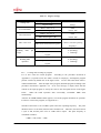
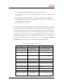
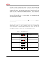
Table 4.1
Setting item
L-level duration
H-level duration
PPG count clock
Enabling
PPG
Register settings
Register for setting (bit)
Value to be set (meaning of
Register name
setting)
PRLL (bits 0 to 7)
0xFA
PPG reload register (L)
(Count: 250)
PRLH (bits 0 to 7)
0xFA
PPG reload register (R)
(Count: 250)
PPG (bits 0 to 7)
0x00
PPG count clock selection register
pin
output
PPGC (bit 13)
PPG operation mode control
register
Enabling PPG
operation
4.4.2
PPGC (bit 15)
PPG operation mode control
register
(Same as internal operating
frequency)
0 (disabling)
1 (enabling)
0 (disabling)
1 (enabling)
Creating and executing of program
Let us now create the actual program.
According to the procedure described in
Appendix A.1, open the source file "main.c" stored in ”sample.prj”, and input the program
portion enclosed by dotted line in the figure below. Use the files other than "main.c"
without modification. After the input of the program, build the program according to the
procedure described in Appendix A.2. If an error message is output, check that the
content of the input program is exactly the same as the description shown in the figure
below.
When the build operation ends successfully, ACCEMIC MDE starts
automatically.
After the ACCEMIC MDE window appears, execute the program and check its operation.
For how to execute the program, see Appendix A.3.
The PPG count clock is set to 2 MHz, equal to the CPU operating frequency. The pulse
duration count is set to 0xFA (250) for both L and H levels. Therefore, the total count of
a cycle is 500, and the pulse wave at 4 kHz will be output. The pulse frequency is
calculated as follows:
2 MHz ÷ 500 (count) = 4 kHz
-60-
© Fujitsu
Table 4.2
Correspondence of counts and pulse frequencies (with operating frequency at 2 MHz)
Count per cycle (L-level duration +
H-level duration)
Pulse frequency
125
16 kHz
250
8 kHz
500
4 kHz
1000
2 kHz
After the PPG pulse output is started by the program and the buzzer starts sounding, the
buzzer sound cannot be stopped even when the stop button on the ACCEMIC screen is
clicked. This is because the PPG timer continues operation and pulse output is not
stopped even when the CPU stops. To stop the buzzer, press the stop button and then
reset the microcomputer.
void main(void){
__set_il(7);
__EI();
IO_PPGC23.bit.PE1=0x01;
(1) Enabling PPG pin output
IO_PPG23.byte=0x00;
(2) PPG count clock setting
IO_PRL23.byte.PRLL3=0xFA;
(3) PPG timer count for L-level
IO_PRL23.byte.PRLH3=0xFA;
(4) PPG timer count for H-level
IO_PPGC23.bit.PEN1=0x01;
(5) Enabling PPG
Program code added
(6) Infinite loop
while(1);
}
Figure 4.8
Program to sound the buzzer
Descriptions ”IO_XXX.byte” and ”IO_YYY.bit” included in the above program code are
the convenient formats of description defined in the I-O header file.
information, see Appendix B.1.
© Fujitsu
-61-
For further
4.4.3
Changing the tone of a buzzer sound
Try to vary the setting of pulse duration to check how the buzzer sound changes. Our
audible frequencies are said to range from 20 Hz to 20 kHz.
Try to confirm the range of
audible frequencies by changing the buzzer sound. Also, the buzzer sound will change
when the PPG count clock is varied. Try to find the reason for the change.
-62-
© Fujitsu
5 “Let's try to control the LED by interrupt.”
A method to detect the switch operation state was described in Chapter 3. There are also other
methods to detect switch operation than the one described in Chapter 3. One of the other
methods is to use an external interrupt input.
This chapter explains how to detect switch
operation by using an external interrupt input.
5.1
What is an interrupt?
Let's begin with a brief explanation of interrupts. The word "interrupt" is popularly used in
daily life, and the meaning of the word is similar when the word is used in the world of
microcomputers.
Imagine that you are studying at home on the day before an examination
day. You need to focus on study but are disturbed by a telephone call from a friend or an
unexpected visitor.
The telephone call and visitor are interrupts.
The microcomputer
terminology names the events like the telephone call and visitor as "interrupt factors" and the
handling of such events as "interrupt processing." Of course, the interrupts in the world of
microcomputers are not telephone calls and visitors but the on/off operation of a switch,
reception of communication data, generation of a timer event, and other various events typical
for microcomputers.
Figure 5.1
Cases of interrupt
In the field of microcomputer and embedded system, using interrupts in programs is generally
regarded as an efficient programming method. In the real word, you cannot predict when
you will receive telephone calls and visitors. You cannot focus on study if you have to often
look at the telephone or get the door to check to see if there is a visitor. Therefore, you
usually keep concentrating on study and interrupt it only when you receive a telephone call or
visitor actually; this is more efficient.
The microcomputer is provided with a mechanism that notifies the microcomputer program of
a switch on/off operation, communication data reception, timer event, or the like
© Fujitsu
-63-
(corresponding to the telephone call or visitor in the real world) when the event occurs. This
mechanism is the interrupt. A program can be efficient when it uses interrupts. The sample
program described in Chapter 3 uses a procedure for checking the on/off state of the switches
cyclically. However, an interrupt is used in the program, the microcomputer can be notified
of a switch on/off operation by the interrupt when the operation occurs. Therefore, the
processing to cyclically check the on/off state of the switches can be eliminated, and the
efficiency of the program can be increased thereby. This chapter explains how to detect
switch operation by using an interrupt and how to create the program for the operation.
5.2
How to detect a switch operation by interrupts
As described in Chapter 3, the board of the Starter Kit has two switches that are connected to
pins P25 and P27 of the microcomputer. Pins P25 and P27 connecting the switches were
used as input ports in the program example described in Chapter 3. These pins can be used
also as external interrupt input pins (INT5 and INT7). The following describes how to detect
switch operation (pressing of a switch) by using an external interrupt input.
Figure 5.2 shows an outline of SW1 connection circuit on the board of the Starter Kit. SW1
is connected to pin INT5 of the microcomputer as shown in Figure 5.2. While SW1 is
released (in the off state), the voltage at pin INT5 of the microcomputer is Vcc (5 V), and the
signal input to pin INT7 is at the high level. When SW1 is pressed (in the on state), the
voltage at pin INT5 becomes the GND level, and the signal input to pin IN5 changes from the
high level to the low level. When SW1 is released subsequently, the signal input to pin INT5
changes from the low level to the high level. When the external interrupt function of pin
INT5 of the microcomputer is used, an interrupt can be generated when the pin status is
changed. In short, this mechanism enables the microcomputer to be informed of switch
operation by the interrupt. SW2 can be handled in a similar way to handle SW1. Because
SW2 is connected to pin INT7 of the microcomputer, an external interrupt is generated at pin
INT7 when SW2 is operated.
Starter Kit board
Vcc
Microcomputer
Pin INT5
(pin P25)
ELVR
EIRR
ENIR
Figure 5.2
SW1
GND
Connection of SW1 to microcomputer pin (conceptual diagram)
-64-
© Fujitsu
Explained next is the procedure for using pin INT5 as an external interrupt pin. To use pin
INT5 for the input of external interrupt, you should set the I-O direction of the pin to input by
using the port 2 register "DDR2." Handling of DDR2 was described in Chapter 3. Write '0'
to the bit 5 of DDR2.
You should also set necessary values in external interrupt registers
"EIRR," "ENIR," and "ELVR" for using pin INT5 as the external interrupt input pin. EIRR
is an 8-bit register that indicates external interrupt factors. ENIR is an 8-bit register that
enables and disables external interrupts.
ELVR is a 16-bit register that specifies the
conditions for external interrupt detection.
Assume the processing to detect the SW1 operation from the off state to the on state by using
an interrupt. When SW1 is pressed, the signal input to pin INT5 changes from the high level
to the low level (as described before). When values are set in external interrupt registers in
steps (1) to (4) below, the external interrupt function enables the microcomputer to detect the
change (falling edge) of the signal input to pin INT5 from the high level to the low level. In
this way, the on operation of SW1 can be detected as the generation of an interrupt.
(1) Write '0' to the bit 5 of both EIRR and ENIR (to disable the external interrupt via
INT5)
(2) Write '1' to the bits 10 and 11 of ELVR (to generate an external interrupt when a
falling edge is detected)
(3) Write '0' to the bit 13 of both EIRR and ENIR (to clear the INT5 interrupt factor)
(4) Write '1' to the bit 5 of both EIRR and ENIR (to enable the external interrupt via
INT5)
5.3
How to create and execute a program to control the LED by switch Input operation
This section explains how to create a program to detect switch operation by an external
interrupt. The program is also designed to operate an LED to enable you to visually see the
detection of switch operation. The program incorporates the method to turn on an LED
explained in Chapter 2.
5.3.1
Outline of the program to be created
Let's create a program to better understand the operation of interrupt processing. This
program will be very similar in contents to the LED control program created in Chapter
2, except that this program will have an additional portion to process the interrupt
generated by switch operation. The main operation by the program is as described
© Fujitsu
-65-
below.
Figure 5.3 shows the flow of the program.
(1) When the program starts, LED1 starts blinking.
(2) When SW1 is pressed, LED3 goes on.
(3) Each time SW1 is pressed, LED3 goes off and on alternately.
The main processing by the program begins with the setting of LED output and switch
input pins. This setting was described in Chapter 3. Next, the program makes the
settings related to the external interrupt and enables the external interrupt. Then, the
program makes LED1 be blinking. Blinking of LED1 continues until the stop or reset
button is pressed on the ACCEMIC screen. When SW1 is pressed after the external
interrupt is enabled, an INT5 interrupt is generated, and an interrupt routine is called.
The interrupt routine clears the interrupt factor and switches LED3 between on and off
states. In summary, this program makes LED1 blinking processing usually as the main
processing, and switches LED3 between the on and off states only when the interrupt is
generated by switch operation.
Start of main processing
Interrupt
Set output pins for LED1 and LED3
(PDR1.bit0 = 0,DDR1.bit0 = 1,
PDR1.bit2 = 0,DDR1.bit2 = 1)
Set input pin for SW1
(DDR2.bit5 = 0)
- - - (2)
Set external interrupt of SW1
(ENIR.bit5 = 0,
ELVR.bit10 = 1, ELVR.bit11 = 1,
ENRR.bit5 = 0)
Enable interrupt.
(ENIR.bit5 = 1)
3000 counted?
Turn on or off LED1
(PDR1.bit0 = !(PDR1.bit0))
- - - (1)
generated
by
SW1
Start of external interrupt processing
Clear external interrupt factor
(ENRR.bit5 = 0)
- - - (7)
Turn on or off LED3
(PDR1.bit2 = !(PDR1.bit2))
- - - (8)
- - - (3)
End of external interrupt processing
- - - (4)
(5)
- - - (6)
Figure 5.3 Flow of the program
-66-
© Fujitsu
5.3.2
Creating and executing of program
Let us now create the actual program.
According to the procedure described in
Appendix A.1, open the source file "main.c" stored in ”sample.prj”, and input the program
portions enclosed by dotted line in Figure 5.4 and Figure 5.5. Use the files other than
"main.c" without modification.
After the input of the program, build the program
according to the procedure described in Appendix A.2.
If an error message is output,
check that the content of the input program is correct. When the build operation ends
successfully, ACCEMIC MDE starts automatically.
After the ACCEMIC MDE window appears, execute the program and check its operation.
For how to execute the program, see Appendix A.3. After the program starts normally,
check LED1. LED1 is blinking when the program is operating normally. Also, press
SW1 to check for normal interrupt operation. The interrupt operation is normal if LED3
goes on and off alternately each time SW1 is pressed.
voi main(void)
{
__set_il(7);
__EI();
Program code added
IO_PDR1.byte = 0x00;
IO_DDR1.byte = 0x1F;
(1) Port 1(LED control) output setting
IO_DDR2.byte = 0x00;
(2) Port 2 (switch input) input setting
IO_ICR06.byte=0x00
IO_ENIR.bit.EN5=0;
IO_ELVA.word=0x0800;
IO_ENRR.bit.ER5=0;
(3) Interrupt-related processing
IO_ENIR.bit.EN5=1;
(4) Enabling interrupt
while(1)
{
for(i=0;i<30000;i++);
(5) LED on/off time count
Setting to use external interrupt
(INT5)
IO_PDR1.bit.P10 = ~ IO_PDR1.bit.P10;
}
(6) LED state change
}
Figure 5.4
© Fujitsu
Sample program code (main routine)
-67-
__interrupt void ext_int(void)
{
IO_EIRR.bit.ER4=0x0;
(7) Interrupt factor clearance
IO_PDR1.bit.P12=~IO_PDR1.bit.P12;
(8) LED on/off switching
}
Program code added
Figure 5.5
Sample program code (interrupt routine)
The ext_int function is called when the external interrupt (INT5) is generated. If you
program the above operation without using this sample project, you should register the
interrupt routine in the vector table so that the ext_int function will be called when the
external interrupt (INT5) is generated. You need not perform the registration when you
use this sample project in which the interrupt routine has already been registered.
Descriptions ”IO_XXX.byte” and ”IO_YYY.bit” included in the above program code are
the convenient formats of description defined in the I-O header file.
For further
information, see Appendix B.1.
-68-
© Fujitsu
6 “Let's blink the LED by using a timer interrupt.”
The procedure for controlling the LED blinking is described in Item 2.5 in Chapter2. There are
some other methods to control the LED blinking other than the method described in Chapter 2.
One of them is the method using a "timer interrupt." This chapter describes the method to control
the LED blinking by using a 16-bit reload timer.
6.1
What is a timer?
Let's begin with a brief explanation of the "timer." The word "timer" is often heard in daily
life, such as a recording timer of VCR, a start timer or sleep timer of the audio system, a
kitchen timer for cooking, or the timer function of an alarm clock. The function of the timer
contained in the microcomputer is the same as those timers.
Let's take the alarm clock timer
as an example to explain the timer function. Most of the people set the alarm clock timer for
a certain time and wake up at the sound of the alarm every morning. What would happen if
there was no alarm timer function? People would be bothered about the time to wake up
once the dawn breaks and could not keep relaxing and sleeping. People can re-realize that
the timer function of the alarm clock allows us to sleep tight until the time to get up.
The microcomputer has the timer interrupt function that performs as an alarm timer function.
In this case, the timer interrupt is used for the LED-on time count and the LED-off time count.
Because the LED blinking control described in Item 2.5 in Chapter2 counts the LED-on time
and LED-off time by executing the CPU instruction, the CPU is always required to perform
the processing for controlling the LED blinking. Figure 6-1 LED blinking processing
without using the timer interrupt shows the LED blinking processing without using the
timer interrupt. This figure shows that the CPU must always control the LED and there is no
time for other processing.
LED-on
LED-off
LED-on time count
CPU processing
Figure 6-1
ON/OFF switching
LED-off time count
ON/OFF switching
LED-on
LED-off
LED-on time count
ON/OFF switching
LED blinking processing without using the timer interrupt
When a timer is used, the timer can take the processing of counting the LED-on and -off
time that is described in Figure 6-1 so that the CPU does not have to count the LED-on and
-off time. The CPU can perform processing other than the LED blinking control accordingly.
© Fujitsu
-69-
Figure 6-2 shows the LED blinking processing with using the timer.
LED-on
CPU processing
LED-off
LED-on
Count not required
Count not required
Count not required
ON/OFF switching
Interrupt processing
ON/OFF switching
Interrupt processing
ON/OFF switching
Interrupt processing
LED-off
Cleared by
Timer interrupt factor
Cleared by software
Cleared by software
software
Number of counts
Timer
Timer counter
Count clock cycle
Figure 6-2 LED blinking processing with using the timer
To use the timer to count the LED-on and -off time, the count clock and the number of the
counts need to be specified. The LED-on and -off time can be calculated by using the
following expression. Using the timer, as just described, has the advantage of enabling the
accurate time count.
LED-on and -off time period = count clock cycle × number of counts
6.2
How to create and execute a program to control the LED blinking by using a timer
interrupt
This section explains how to create a program to control the LED blinking by using a timer
interrupt. The 16-bit reload timer is used for the timer of this program.
6.2.1
Outline of the program to be created
In Chapter 2, the LED blinking time is controlled by a WAIT of the loop processing.
In this section, a program that uses the 16-bit reload timer interrupt to count the LED blinking
time is created. The LED operation of this program is the same as that of the program
created in Chapter 2. However, as the operation of the microcomputer, the 16-bit reload
timer instead of the CPU is used for counting the LED-on and -off time. The CPU is not
-70-
© Fujitsu
required for counting the LED-on and -off time.
Figure 6-3 Flow of the program shows the flow of the program.
Timer interrupt is generated.
Start of main processing
Set LED5 to "on."
Set P14 output level to "Low."
Timer interrupt processing starts.
(1)
Set P14 to output mode.
(DDR1.bit4 = 1)
(2)
Set CPU interrupt level.
(3)
Set interrupt permission.
(4)
Set timer interrupt level.
(5)
Set timer count value.
(6)
Set timer count clock.
(7)
Set timer count repeat.
(8)
Timer interrupt permission
(9)
(13)
ON/OFF switching of LED5
(14)
Timer interrupt processing ends.
Timer operation permission (wait for a start factor)
(10)
Software start factor of timer (starts operation)
(11)
Infinite loop
Timer interrupt factor is cleared.
(12)
Figure 6-3
Flow of the program
The program created in this section goes into an infinite loop (No. 12 in the flow of the
program) after a sequence of the processing. During this infinite loop processing, the
CPU can execute any processing other then the LED processing. Table 6-1 Register
setting of 16-bit reload timer shows the register of the 16-bit reload timer that is set in
the program created in this section. Suppose the LED-on and -off time is one second.
The value to be set for the counter of the 16-bit reload timer can be calculated by using
the following expression accordingly.
LED -on and -off time period = Count clock cycle (16 µs) × Number of counts (62500)
=1s
© Fujitsu
-71-
Table 6-1
Setting item
Timer count value
Timer count clock
Register name
Setting bit
TMRLR register
D0 to D15 (bit0 to bit15)
TMCSR0 register
CSL0, CSL1(bit10, bit11)
TMCSR0 register
Timer count repeat
Timer interrupt
permission
Timer interrupt
factor
Timer operation
permission
Timer software start
Register setting of 16-bit reload timer
RELD (bit4)
TMCSR0 register
INTE (bit3)
TMCSR0 register
UF (bit2)
TMCSR0 register
CNTE (bit1)
TMCSR0 register
TRG (bit0)
Setting value (meaning)
0 × F424 (62500 counts)
10 (count clock cycle: 16 µs)*
0 (Timer stops at an interrupt generation.)
1 (Timer count is reset at an interrupt generation and
the operation continues.)
0 (Timer interrupt permitted)
1 (Timer interrupt not permitted)
0 (There is no timer interrupt factor.)
1 (There is a timer interrupt factor.)
0 (Not permitted)
1(Permitted)
0 (No effect)
1 (Start)
* Count clock cycle (16 µs) = 32 / Internal operation frequency (2 MHz)
6.2.2
Creation and execution of the program
Let us now create the actual program.
According to the procedure described in
Appendix A.1, open the source file "main.c" in sample.prj and input the program that is
the circled part in Figure 6-4 Example of program code (main routine) and Figure 6-5
Example of program code (interrupt routine).
Use all files except main.c without any
changes. After the program is input, "build" the program according to the procedure
described in Appendix A.2.
If an error is output, reconfirm that the program accords to the contents of Figure 6-4
Example of program code (main routine) and Figure 6-5
(interrupt routine).
Example of program code
When the "build" is succeeded, "ACCEMIC MDE" starts
automatically.
When the "ACCEMIC MDE" window appears, execute the program and check the
operation. For the procedure of the program execution, see Appendix A.3. When the
program starts correctly, check LED5. Blinking LED5 indicates the normal operation.
-72-
© Fujitsu
void main(void)
{
IO_PDR1.byte=0xEF;
(1) LED5 on setting P14=Low
IO_DDR1.byte=0x1F;
(2) P10 to P14 output setting
__set_il(7);
(3) CPU interrupt level setting
__EI();
(4) Interrupt permission
IO_ICR03.byte=0x06;
(5) Timer interrupt level setting
IO_TMR[0]=0xF424;
(6) Timer count value setting
IO_TMCSR0.bit.CSL=2;
(7) Timer count clock setting
IO_TMCSR0.bit.RELD=1;
(8) Timer count repeat setting
IO_TMCSR0.bit.INTE=1;
(9) Timer interrupt permission
IO_TMCSR0.bit.CNTE=1;
IO_TMCSR0.bit.TRG=1;
while(1);
}
(10) Timer operation permission (wait for
a start factor)
(11) Software start factor of timer (starts
operation)
(12) Infinite loop
Program code to be added
Figure 6-4 Example of program code (main routine)
__interrupt void reload_int(void)
{
IO_TMCSR0.bit.UF = 0;
(12) Clearing interrupt factor
IO_PDR1.bit.P14=~IO_PDR1.bit.P14;
}
(13) LED-on/off switching
Program code to be added
Figure 6-5 Example of program code (interrupt routine)
The reload_int function in Figure 6-5
Example of program code (interrupt routine) is
to be executed when an interrupt of the 16-bit reload timer is generated. It is normally
required to register the interrupt routine on the vector table so that the reload_int function
is executed when an interrupt of the 16-bit reload timer is generated. In this sample
project, however, it has already been registered, so it can be used without registration.
In the above code, there are some expressions such as "IO_XXX.byte" and "IO_YYY.bit".
These are the useful description formats, which are defined in the IO header file. For
more information, see the Appendix.
© Fujitsu
-73-
7 “Let's use the A/D converter.”
This section describes the processing to convert the analog signals input to the microcomputer into
the digital signals by using the A/D converter and to load the digital signals into the
microcomputer.
This Starter Kit can control the value of the voltage applied to the analog pin for the A/D converter
by using the volume tab mounted on the board.
Let's input the analog signal to the
microcomputer by using this tab. The input analog signal can be converted into the digital signal
by the A/D converter and processed by the microcomputer.
Volume tab for
adjusting applied voltage
Figure 7-1
7.1
Adjustment of applied voltage with volume tab
Analog and Digital
Do you know the difference between analog and digital? Those are explained as follows in a
dictionary.
Table 7.1
Analog and digital
Definition in a dictionary
Analog
Digital
Expressing states of a material or system according
to its physical quantity that varies continuously
Expressing states of a material or system according
to discrete signals such as numbers or characters
Although you read the above definitions, you may have a hard time picturing them.
Intuitively speaking, initially, everything is in analog value. At the moment a person tries to
determine the size or variety of the analog value, the quantity becomes digital value. In other
words, a digital value exists only when an analog value exists. A digital value is what an
analog value is divided into some levels for easier handling and converted to easier
-74-
© Fujitsu
understandable form.
Figure 7-2
Low accurate digital conversion shows an example of analog and digital
signals. The blue line indicates an analog signal, and the black line indicates a digital signal.
The digital signal in this figure is a low accurate A/D conversion result.
Figure 7-2
7.1.1
Low accurate digital conversion
Outline of A/D converter
A digital value is a value into which an analog value is divided according to a standard
based on a certain rule. The A/D converter is mounted on the microcomputer to
perform this conversion. For this conversion, the important factor is resolution. This
resolution is, like the resolution of photograph, a scale of how small the analog value is
to be resolved and converted to the digital value. For example, a school record that is
evaluated on a scale of one to five can be a poor accurate digital value. In contrast, a
school record that is evaluated on full mark of a 1000-point scale can be a highly
accurate digital value.
The microcomputer mounted on this Starter Kit contains the A/D converter that has
10-bit resolution (8-bit resolution is also available).
Having the 10-bit resolution
10
means that it can resolve an analog value into 2 , or 1024, levels to convert it to a
digital value (with 8-bit resolution, the value is resolved into 28, or 256, levels). The
higher the resolution is, the more highly the A/D conversion can be accurate. The
following shows the 1-bit voltage accuracy (at 5 V) with 10-bit resolution and 8-bit
resolution.
1-bit voltage accuracy (at 5 V)
10-bit resolution:
8-bit resolution:
© Fujitsu
5 V/1024 = approximately 0.00488 V
5 V/256 = approximately 0.01953 V
-75-
7.1.2
Scheme of volume tab
Figure 7-3
Variable resistor shows the symbol of a variable resistor.
The volume is
the variable resistor that you use in an experiment in a science class. This Starter Kit
uses the circuit configuration shown in
Figure 7-4
Peripheral circuitry of voltage adjustment. By using this tab, the
voltage is changed and applied to the target pin of the A/D conversion. The applied
voltage is digitized into 1024 levels so that it can be used as an internal signal.
Figure 7-3
Variable resistor
Starter Kit board
Vcc
Microcomputer
Pin AN1
(Variable resistor)
Volume
ADCS
ADCR
Figure 7-4
7.2
GND
GND
Peripheral circuitry of voltage adjustment tab
How to create and execute a program to display potental
Let's create a program to display the potential based on the contents so far. Input the
adjusted voltage, convert the analog signal to digital, and obtain the digital value. Also, light
the LED to display the potential.
7.2.1
Outline of program to be created
Let us now create the actual program. The contents of the program are to use the A/D
converter to digitalize the potential of the applied voltage and to determine the number
of LEDs to be lighted according to the potential. The main operation of the program is
described below.
The flow of the program is shown in Figure 7-5
Flow of the
program .
-76-
© Fujitsu
(1) Perform initialization (such as initial settings of the A/D converter).
(2) Start the A/D conversion (to obtain the applied voltage by using the A/D
converter).
(3) The A/D conversion is completed.
(The A/D converted values are obtained.)
(4) Light the LEDs according to the obtained A/D converted values. (Determine the
number of LEDs to be lighted.)
(5) Then, repeat (2) to (4).
First, in the program, set up the output pin of the LED and the input pin to be used for the
A/D converter.
Then, make the settings regarding the A/D converter operations such as
the sampling time of the A/D conversion, operation mode, and A/D input channels. In
this section, the sampling time is set to 128/φ, the comparing time is set to 176/φ, the
resolution is set to 8-bit、and the A/D conversion channel to be used is set to Ch0 only,
and the operation mode is set to the continuous conversion mode. "φ" indicates the
internal operation frequency of the microcomputer. Table 7.2 Register settings of
A/D converter shows the values to be written to the register for the settings.
Table 7.2
Register settings of A/D converter
Item
Register (bit)
Setting value (contents)
A/D conversion started
ADCS: H (bit 9)
1 (A/D conversion started)
A/D interrupt permission
ADCS:H (bit 13)
1 (permitted), 0 (not permitted)
A/D interrupt factor
ADCS: H (bit 14)
0 (factor cleared)
ADCS:H (bit 15)
0 (A/D conversion is forcibly
cleared
A/D conversion stopped
stopped)
A/D conversion end Ch
ADCS: L (bits 0 to 2)
0 (Select Ch0)
A/D conversion start Ch
ADCS: L (bits 3 to 5)
0 (Select Ch0)
A/D conversion mode
ADCS: L (bits 6 to 7)
2 (Continuous conversion mode)
setting
Comparing time selection
ADCR: H (bits 11 to 12)
3 (176/φ)
Sampling time selection
ADCR: H (bits 13 to 14)
3 (128/φφ)
A/D resolution selection
ADCR: H (bit 15)
1 (8-bit resolution)
Analog input permission
ADER (bits 0 to 7)
01h (Input permitted from Ch0
only)
© Fujitsu
-77-
*The sampling time includes the time for loading the A/D input voltage after
the A/D conversion starts.
*The comparing time is the time to perform comparison operations of the sampled A/D voltage
and the standard voltage of the A/D converter and to convert it to a digital value.
After that, permit interruptions of A/D converter.
This is the end of the operation
settings of the A/D converter. Start the A/D conversion. In this program, the operation
mode of the A/D converter is set to the continuous conversion mode. The operation of
the A/D converter is as follows accordingly.
A/D converter is activated (A/D conversion starts) ⇒ A/D conversion ends ⇒ A/D
conversion starts - - -
The operation repeats as shown above. When the A/D conversion ends, an interrupt of
the A/D converter is generated, and an interrupt routine is called. In the interrupt routine,
the interrupt factor is cleared, the A/D value is obtained, and the LEDs are lighted
according to the obtained A/D value, which is the volume size. The correspondence
between the volume size and the number of LEDs lighted is as shown in Table 7.3 LED
lighting according to volume .
Table 7.3
LED lighting according to volume level
Applied voltage
Obtained A/D value
0 to 0.83 V
0 to 43
0.83 to 1.67 V
43 to 85
1.67 to 2.50 V
85 to 128
2.50 to 3.33 V
128 to 171
3.33 to 4.17 V
171 to 213
4.17 to 5.00 V
213 to 255
-78-
LED lighting
No LED is on.
LED1 is on.
LEDs 1 to 2 are on.
LEDs 1 to 3 are on.
LEDs 1 to 4 are on.
All LEDs are on.
© Fujitsu
Interrupt occurs by A/D conversion end
Start of main processing
External interrupt processing starts.
Set output pins of LED1 to LED5.
(PDR1.byte = 0x1F,
DDR1.byte = 0x1F)
(1)
Set an input pin of AN1
(DDR5.bit1 = 0)
(2)
Stop A/D converter.
(ADCS:H.bit15 = 0)
(3)
Initialize the A/D converter.
Set the channel. (ADER.byte=0x01)
Set the mode (continuous conversion,
(ADCS:L.byte = 0x80)
Set the sampling conditions.
(ADCR:H.byte = 0xF8)
External interrupt factor is cleared.
(ADCS:H.bit14 = 0)
(7)
Turns on/off LED3.
(PDR1.bit2 = !(PDR1.bit2))
(8)
Obtain A/D value.
(AD_DATA = ADCR:L.byte)
AD_DATA<42
Y
N
(4)
AD_DATA<84
A/D converter interrupt permission
(ADCS:H.byte13 = 1)
(5)
A/D conversion started
(ADCS:H.byte9 = 1)
(6)
LED lighting processing
(PDR1.byte = 0x1F)
Y
N
AD_DATA<126
LED lighting processing
(PDR1.byte = 0x1E)
Y
N
Infinite loop
AD_DATA<168
LED lighting processing
(PDR1.byte = 0x1C)
Y
N
AD_DATA<210
N
LED lighting processing
(PDR1.byte = 0x00)
External interrupt processing ends
Figure 7-5
© Fujitsu
Flow of the program
-79-
(9)
LED lighting processing
(PDR1.byte = 0x18)
Y
LED lighting processing
(PDR1.byte = 0x010)
7.2.2
Creation and execution of the program
Let us now create the actual program.
According to the procedure described in
Appendix A.1, open the source file "main.c" in the "sample.prj," and input the program
that is the circled part in Figures A.1 and A.1. Use all files except main.c without any
changes. After the program is input, "build" the program according to the procedure
described in Appendix A.2.
If an error is output, reconfirm that the program accords to
the contents of Figure 6-4 Example of program code (main routine) and Figure 6-4
Example of program code (main routine).
When the "build" is succeeded, “
ACCEMIC MDE” starts automatically.
When the “ACCEMIC MDE” window appears, execute the program and check the
operation. For the procedure of the program execution, see Appendix A.3. When the
program starts correctly, check the operation. It can be confirmed that the LEDs 1 to 5
are lighted according to the size of the applied voltage that has been adjusted on the
volume.
voi main(void)
{
__set_il(7);
__EI();
Program code to be added
IO_PDR1.byte = 0x1F;
IO_DDR1.byte = 0x1F;
(1) Port 1 (LED control) output setting
IO_DDR5.bit.D50 = 0;
IO_ICR03.byte = 0x06;
(2) Port 5 (AD input) input setting
IO_ADCSH.bit.BUSY = 0;
(3) Stop A/D converter.
IO_ADER.byte = 0x01;
IO_ADCSL.byte = 0x80;
IO_ADCRLH.byte.ADCRH = 0xF8;
(4) A/D converter initialization
IO_ADCSH.bit.INTE = 1;
IO_ADCSH.bit.STRT = 1;
- A/D converter channel setting
- A/D converter mode setting
- A/D sampling condition setting
(5) A/D conversion
interrupt permission
(6) A/D conversion starts
while(1);
}
Figure 7-6
Example of program code (main routine)
-80-
© Fujitsu
__interrupt void ADC_int(void)
{
Program code to be added
unsigned char AD_DATA;
IO_ADCSH.bit.INT = 0;
(7) Clearing interrupt factor
AD_DATA = IO_ADCRLH.DATA8;
(8) Obtain A/D converted value.
if(AD_DATA > 171){
(9) LED control based on AD value.
IO_PDR1.byte = 0x1F;
}
else if(AD_DATA > 142){
IO_PDR1.byte = 0x1E;
}
else if(AD_DATA > 113){
IO_PDR1.byte = 0x1C;
}
else if(AD_DATA > 87){
IO_PDR1.byte = 0x18;
}
else if(AD_DATA > 66){
IO_PDR1.byte = 0x10;
}
else{
IO_PDR1.byte = 0x00;
}
}
Figure 7-7
Example of program code (interrupt routine)
The ADC_int function is to be executed when an interrupt of the A/D converter is generated.
It is generally required to register the interrupt routine on the vector table so that the
ADC_int function is executed when an interrupt of the A/D converter is generated. In
this sample project, however, it has already been registered, so it can be used without the
registration.
In the above code, there are some expressions such as "IO_XXX.byte" or "IO_YYY.bit."
These are the useful description formats, which are defined in the IO header file. For
more information, see the Appendix.
© Fujitsu
-81-
8 “Let's use the temperature sensor.”
Most of the microcomputer application systems contain various sensors to detect the external
information. There are various sensors for different purposes and requirements, and one of those
various sensors is the temperature sensor. The temperature sensor is, as its name suggests, a
sensor to detect changes in temperature. Examples of what the temperature sensor is used for
include the temperature control features of air conditioners and refrigerators. In this way, various
sensor s are used for household appliances.
This Starter Kit contains the temperature sensor.
This chapter describes how to detect
temperature by using this temperature sensor.
8.1
What is a temperature sensor?
The temperature sensor is a sensor to detect temperature changes. Simply stated it is a
thermometer to measure temperature. There are various methods to measure temperature. One
of those methods uses a mercurial thermometer, and another one uses a radiation thermometer
that enables contactless measurement. Table 8.1 Temperature measuring method shows
the general methods for measuring temperature. Of course it depends on the purposes or
requirements, however, most of the systems containing microcomputers use the thermocouple
thermometer or thermistor. This Starter Kit also uses the thermistor as its temperature sensor.
Table 8.1
Temperature measuring method
Category
Method and its feature
Mercurial/alcohol
This method uses thermal expansion of mercury or alcohol to detect
thermometer
temperature. This method is used for many thermometers and
clinical thermometers.
Thermocouple
This sensor uses the Seebek effect.
It contains the two-contact
thermometer
circuit using two different metals, and when there is a difference in
temperature between two contact points, it generates thermal
electromotive force. It can measure the wide-range temperature.
Thermistor
This sensor uses the resistance thermometer bulb that uses the
temperature characteristic of semiconductor. It is in heavy usage.
Radiation
The infrared energy emitted by an object varies with temperature.
thermometer
The radiation thermometer uses this principle for measuring
temperature. It enables contactless measurement.
-82-
© Fujitsu
The thermistor is the resistor using the temperature characteristic of semiconductor. The
resistance value of the temperature sensor varies with temperature. This Starter Kit contains
the TDK's NTC thermistor (NTCG164BH103) for its temperature sensor. NTC stands for
Negative Temperature Coefficient, and this thermistor has negative characteristic of the
resistance value, which is reduced as the temperature rises.
This section describes the
concrete method of detecting temperature by using this temperature sensor.
Temp. sensor
Figure 8-1
8.2
Temperature sensor (NTCG164BH103)
How to detect temperatures by using "temperature sensor"
To use the temperature sensor and detect temperature, it is necessary to understand the
specifications of the sensor. The specifications of the sensor to be used (NTCG164BH103)
can be confirmed on the sensor data sheet, which is issued from the manufacturer. The data
sheet of the temperature sensor contains the information required for measurement. For this
time, the relationship between the measured temperature and the state of the sensor (resistance
value) is especially important. According to the data sheet, the relationship between the
temperature from 5 to 50 oC and the resistances are shown in Table 8.2 Relationship
between measured temperature and resistance of NTCG164BH103.
Table 8.2
© Fujitsu
Relationship between measured temperature and resistance of NTCG164BH103
Temperature[°C]
Resistance value[kΩ]
Temperature[°C]
Resistance value[kΩ]
5
26.250
30
7.997
10
20.390
35
6.437
15
15.960
40
5.213
20
12.590
45
4.248
25
10.000
50
3.481
-83-
Figure 8-2 Peripheral circuit diagram of "temperature sensor" (image)
shows the peripheral circuit diagram of the "temperature sensor" on the Starter Kit board. In this
circuit, when the resistance of the "temperature sensor" changes, the input voltage of the A/D
converter of the microcomputer also changes. Suppose the resistance of the "temperature sensor" is
RTH . Then, the input voltage of the A/D converter VAN1 can be calculated by using the following
formula. (The necessary knowledge to calculate it is only Ohm's law.)
Starter Kit board
Vcc
Microcomputer
R=10 kΩ
Pin AN1
Temperature
sensor
AD
AD
Figure 8-2
GND
GND
Peripheral circuit diagram of "temperature sensor" (image)
[Input voltage of the A/D converter]
According to the Ohm's law, the current in the circuit I is as shown below:
I=
VCC
R + RTH
Vcc=5.0[V]
Therefore, VAN1 is
V AN 1 = RTH
R=10[kΩ]
R ×V
× I = TH CC
R + RTH
VAN1
I
RTH
GND
Because R=10[kΩ] and Vcc=5.0[V],
the input voltage to the A/D converter VAN1[V] can be obtained by using the following
formula.
V AN 1 =
Table 8.3
5.0 × RTH
10000 + RTH
Relationship between the measured temperature of Starter Kit and A/D input
voltage summarizes the relationship between the measured temperature from 5 to 50 oC and
-84-
© Fujitsu
the input voltage of the A/D converter. By measuring the input voltage of the A/D converter,
the temperature can be known accordingly.
Table 8.3
Relationship between the measured temperature of Starter Kit and A/D input voltage
Temperature [°C]
A/D input voltage:
Temperature [°C]
VAN1[V]
8.3
A/D input voltage:
VAN1[V]
5
3.62
30
2.22
10
3.35
35
1.96
15
3.07
40
1.71
20
2.79
45
1.49
25
2.50
50
1.29
How to create and execute a program to display temperature
The following section explains how to create a program to detect temperature by using the
sensor. For how to use the A/D converter, apply the contents of the previous chapter. For
checking the detected temperature visually, the lighting of the AD input LED is controlled.
8.3.1
Outline of the program to be created
Let us now create the actual program. The contents of the program are to use the A/D
converter to obtain the temperature information of the sensor, and to control the lighting
of the LED (to change the lighting pattern) according to the obtained value. For
processing related to the A/D converter, create the program based on the program of the
volume control A/D converter that is created in the previous chapter. The main
operation of the program is described below. The flow of the program is shown in
Figure 8-3 Flow of the program
(1) After the program is started, performs the initialization (such as initial settings of the
A/D converter).
(2) Starts A/D conversion (to obtain the sensor information using the A/D converter).
(3) The A/D conversion is completed. (The A/D converted values are obtained.)
(4) According to the obtained A/D converted values, controls the LED lighting.
(5) Then, repeat (2) to (4).
© Fujitsu
-85-
In the flow of the main processing of the program, first set up the output pin of the LED
and the input pin to be used for the A/D converter. The settings of the pins are explained
in the previous chapter. Then, make the settings related to the A/D converter. The
settings to be made are about the same as the previous chapter. The only difference is
that the channel of the A/D converter to be used is set to "1" (Channel 0 is used in the
previous chapter). The operation mode of the A/D converter is set to the continuous
conversion mode that is also used in the previous chapter. The operation of the A/D
converter is as follows accordingly.
A/D converter is activated (A/D conversion starts) ⇒ A/D conversion ends ⇒ A/D
conversion starts - - -
When the A/D conversion ends, an interrupt of the A/D converter is generated, and an
interrupt routine is called. In the interrupt routine, the interrupt factor is cleared, the A/D
value is obtained, and the LEDs are lighted according to the obtained A/D value. The
LED lighting processing is as shown in Table 8.4
Table 8.4
Obtained A/D value
LED lighting processing.
LED lighting processing
LED lighting
Remarks
50 oC or higher
0 to 65
All LEDs are on.
40 oC or higher but lower than 50 oC
66 to 86
LEDs 1 to 4 are on.
30 oC or higher but lower than 40 oC
87 to 112
LEDs 1 to 3 are on.
20 oC or higher but lower than 30 oC
113 to 141
LEDs 1 to 2 are on.
10 oC or higher but lower than 20 oC
142 to 170
LED 1 is on.
Lower than 10 oC
171 to 255
No LED is on.
-86-
© Fujitsu
Interrupt occurs by A/D conversion end
Start of main processing
External interrupt processing starts
Set output pins of LED1 to LED5.
(PDR1.byte = 0x1F,
DDR1.byte = 0x1F)
(1)
Set an input pin of AN1.
(DDR5.bit1 = 0)
(2)
Stop the A/D converter
(ADCS:H.bit15 = 0)
(3)
Initialize the A/D converter.
Set the channel (ADER.byte = 0x02)
Set the mode (continuous conversion
(ADCS:L.byte = 0x89)
Set the sampling conditions
(ADCR:H.byte = 0xF8)
External interrupt factor is cleared
(ADCS:H.bit14 = 0)
(7)
Turns on/off LED3
(PDR1.bit2 = !(PDR1.bit2))
(8)
Obtain A/D converted value.
(AD_DATA = ADCR:L.byte)
AD_DATA>171
Y
N
(4)
AD_DATA>142
A/D converter interrupt permission
(ADCS:H.byte13 = 1)
(5)
A/D conversion started
(ADCS:H.byte9 = 1)
(6)
LED lighting processing
(PDR1.byte = 0x1F)
Y
N
AD_DATA>113
LED lighting processing
(PDR1.byte = 0x1E)
Y
N
Infinite loop
AD_DATA>87
LED lighting processing
(PDR1.byte = 0x1C))
Y
N
AD_DATA>66
N
LED lighting processing
(PDR1.byte = 0x00)
External interrupt processing ends.
Figure 8-3
© Fujitsu
Flow of the program
-87-
(9)
LED lighting processing
(PDR1.byte = 0x18)
Y
LED lighting processing
(PDR1.byte = 0x010)
8.3.2
Creation and execution of the program
Let us now create the actual program. According to the procedure described in Appendix
A.1, open the source file "main.c" in "sample.prj," and input the program that is the
circled part in Figure 8-4 Example of program code (main routine)
and Figure 8-5 Example of program code (interrupt routine)
Use all files except main.c without any changes. After the program is input, "build" the
program according to the procedure described in Appendix A.2. If an error is output,
reconfirm that the contents of the program are correct. When the "build" is successful,
"ACCEMIC MDE" starts automatically.
When the "ACCEMIC MDE" window appears, execute the program and check the
operation. For the procedure of the program execution, see Appendix A.3. When the
program starts correctly, check the LEDs. When the temperature of the room where the
operation is performed is between 10 and 20 oC, LED 1 and LED 2 are supposed to be on.
The number of LEDs lighted varies with the temperature detected by the sensor. For
example, warm up the sensor part using your fingers. When warming up the peripheral
part of the sensor, be aware of the temperature. When it gets hot, it may damage the
board.
voi main(void)
{
__set_il(7);
__EI();
Program code to be added
(1) Port 1 (LED control) output setting
IO_PDR1.byte = 0x1F;
IO_DDR1.byte = 0x1F;
IO_DDR5.bit.D51 = 0;
IO_ICR03.byte = 0x06;
(2) Port 5 (AD input) input setting
IO_ADCSH.bit.BUSY = 0;
(3) Stop A/D converter
IO_ADER.byte = 0x02;
IO_ADCSL.byte = 0x89;
IO_ADCRLH.byte.ADCRH = 0xF8;
(4) A/D converter initialization
IO_ADCSH.bit.INTE = 1;
IO_ADCSH.bit.STRT = 1;
- A/D converter channel setting
- A/D converter mode setting
- A/D sampling condition setting
(5) A/D conversion
interrupt permission
(6) A/D conversion starts.
while(1);
}
Figure 8-4
Example of program code (main routine)
-88-
© Fujitsu
__interrupt void ADC_int(void)
{
Program code to be added
unsigned char AD_DATA;
IO_ADCSH.bit.INT = 0;
(7) Clearing interrupt factor
AD_DATA = IO_ADCRLH.DATA8;
(8) Obtain A/D converted value
if(AD_DATA > 171){
(9) LED control based on AD value
IO_PDR1.byte = 0x1F;
}
else if(AD_DATA > 142){
IO_PDR1.byte = 0x1E;
}
else if(AD_DATA > 113){
IO_PDR1.byte = 0x1C;
}
else if(AD_DATA > 87){
IO_PDR1.byte = 0x18;
}
else if(AD_DATA > 66){
IO_PDR1.byte = 0x10;
}
else{
IO_PDR1.byte = 0x00;
}
}
Figure 8-5
Example of program code (interrupt routine)
The ADC_int function is to be executed when an interrupt of the A/D converter is generated.
It is normally required to register the interrupt routine on the vector table so that the
ADC_int function is executed when an interrupt of the A/D converter is generated. In this
sample project, however, it has already been registered, so it can be used without
registration.
In the above code, there are expressions such as "IO_XXX.byte" or "IO_YYY.bit." These are the
useful description formats, which are defined in the IO header file. For more information, see the
Appendix.
© Fujitsu
-89-
A Appendix (Program Creation Procedure)
A.1
Program Creation Procedure
This appendix explains the procedure you should follow when creating an actual program.
First, start up SOFTUNE as instructed in Item 1.1.5, "Starting and setting up of SOFTUNE,"
(pages 15 to 17), and open the Start_kit.wsp file. Use the sample project provided for easy
creation of software.
To use the sample project, select "Sample.prj" in the list, right-click to open a submenu, and
select 'Set active project' from the submenu. Then, the string including "Sample.prj" is
displayed in boldface in the list, and debugging of the sample project is enabled.
Sample project
Select 'Set active project.'
-90-
© Fujitsu
Click on "Sample.prj" to show the list of folders below. Click on "main.c" under the Source
Files folder to open the main.c file.
After the main.c file is opened, create your program in the section indicated by the red dotted
line below.
#include "_ffmc16.h"
#include "extern.h"
//#include "monitor.h"
void main(void)
{
Input the program to be created here.
}
/* Vector Table */
#pragma section INTVECT,locate=0xfffc00
#pragma intvect _start
0x8 0x0
// Reset Vector
If another program has already been input to the main.c file, delete the lines from the above
program list section enclosed by the red dotted line before creating your new program.
If
you need to save the already input program, perform the procedure below to save the program
as a backup file before deleting the program.
© Fujitsu
-91-
<Program (source file) backup procedure>
While editing a source file, select 'Save As...(A)' from the File menu.
The dialog box below appears.
Select Text file, and then click 'OK.'
Next, the dialog box below appears. Select the folder to save the program in the Save in
field, specify the file name in the File name field, and then click 'Save.'
-92-
© Fujitsu
The saved file is still displayed.
Close the displayed file.
Name of the saved file
(main_old.c) is
displayed.
After closing the saved file, find the original file name of the saved file ("main_old.c in this
example) in the Source Files folder under "Sample.prj" in the list, and then click on the
original file name to open the file.
© Fujitsu
In this status, you can edit the source file.
-93-
A.2
Program Building Procedure
After creating a program, confirm that the board is connected to the personal computer by the
USB cable, and then start the procedure to build the program.
If no error is found in the created program, ACCEMIC MDE starts automatically and displays
the information shown below for 10 s. This information is displayed only by the trial version
of ACCEMIC MDE (not displayed by the product version). An 'OK' button appears 10 s
later.
Click the OK button.
-94-
© Fujitsu
If an error is found in the created program, the error is indicated as shown below. Correct the
indicated error, and perform 'building' again.
Click the error code to jump to
the line that includes the error.
Error indication window
© Fujitsu
-95-
A.3
Program Execution Method
Execute the created program and check that it performs the intended operation.
After
ACCEMIC MDE has started, the window as shown below appears:
Use the buttons shown below to control the program.
Function
Continuous
Button
Operation (when clicked)
Starts and runs the program continuously.
execution
Stop
Stops the running program.
Reset
Resets the microcomputer.
-96-
© Fujitsu
B Appendix (Method To Write/Read Values in Registers)
B.1
About the Method To Write/Read Values in Registers
The sample program codes presented in this document include such descriptions
as ”IO_XXX.byte” and ”IO_YYY.bit”. These are the convenient formats of description
defined in the I-O header file. You can use these description formats after setting up Softune
Workbench, the development environment provided by the Starter Kit.
An actual C-language program contains the descriptions of instructions to write values to
various registers to specify microcomputer operation. The above description formats enable
you to write values to registers in C language. For example, assume the instruction to write
0xff to the port 1 data register (PDR1), which is allocated at address 0x000001.
The
instruction is described in C language as follows:
*((volatile char *)0x000001) = 0xFF;
It is not immediately obvious what kind of processing the above description specifies.
If you
use one of the description formats defined in the I-O header file, you can write the same
instruction as follows:
IO_PDR1.byte = 0xff;
You can use this description because the following operation is defined in a separate file:
Substituting a value for variable "IO_PDR1.byte" = Writing the value to PDR1 register at
address 0x000001
It is now immediately clear that the description specifies the processing to write 0xff to the
PDR1 register. The I-O header file contains the definitions of these description formats for
the registers of the microcomputer built in the Starter Kit.
© Fujitsu
-97-
C Appendix (Method To Change the Include Path)
C.1
About the Method To Change the Include Path
A necessary include path is specified for each sample program.
A sample program requires the specified include path to reference sample I-O register
files.
If the installation folder of SOFTUNE or ACCEMIC MDE is changed, change the include
path settings of the C compiler and the assembler before using the sample program.
Select "Project setting(J)" under "Project(P)."
Change the include path settings of the C compiler and the assembler as shown below.
The following window shows the include path setting of the C compiler.
Select this tab for setting
the include path of the C.
Delete the specified
include path.
-98-
© Fujitsu
Click this button to
select a arbitrary
directory.
Select a folder.
Click the Add button to
add the selected include
path.
After setting, click the
OK button.
© Fujitsu
-99-
Use the same procedure for setting the include path of the assembler.
Select this tab for setting
the include path of the
assembler.
-100-
© Fujitsu