1
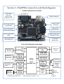
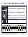
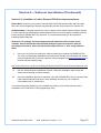
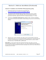
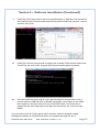
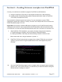
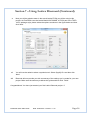
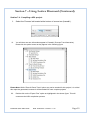
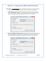
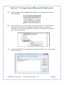
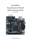
FleaFPGA
Experimenters Board
Quick Startup Guide
Revision 0.13
www.fleasystems.com
Contents:
SECTION 1 – WARRANTY AND LEGAL INFORMATION ........................................................................................ 3
SECTION 2 – INTRODUCTION............................................................................................................................ 4
SECTION 3 – FLEAFPGA CONNECTIVITY AND BLOCK DIAGRAMS ......................................................................... 5
SECTION 4 – FLEAFPGA HARDWARE OVERVIEW ................................................................................................ 6
SECTION 5 – SOFTWARE INSTALLATION ............................................................................................................ 8
SECTION 6 – LOADING PRE-BUILT FIRMWARE INTO FLEAFPGA ........................................................................ 13
SECTION 7 – USING LATTICE DIAMOND ......................................................................................................... 14
SECTION 8 – WHERE TO FROM HERE? ............................................................................................................. 25
SECTION 9 – NOTES ....................................................................................................................................... 27
SECTION 10 – NOTES ..................................................................................................................................... 28
SECTION 11 – NOTES ..................................................................................................................................... 29
APPENDIX A – FLEAFPGA SPECIFICATIONS ...................................................................................................... 30
APPENDIX B – FLEAFPGA BOARD SCHEMATICS ............................................................................................... 31
FleaFPGA Quick Start Guide
Date: 22/04/2014 Revision: 0.13
Page 2
Section 1 – Warranty and legal information
Product Warranty and Liability:
FleaFPGA Experimenters Board is warranted against defects in materials and workmanship for
a period of 90 days from the date-of-purchase. At its discretion, Fleasystems will repair or
replace a FleaFPGA Experimenters Board where it has found defective due to quality control or
manufacturing error. In the case of a valid warranty claim, Fleasystems will cover the repair cost
of a defective FleaFPGA Experimenters board and only pay for return shipping via standard
mail. In all other instances the user shall pay all shipping and repair costs.
This warranty does not cover product damage or destruction due to improper use i.e. operating
FleaFPGA beyond stated electrical and thermal limits or through physical abuse. The user
assumes all responsibility and liability for proper and safe handling of the goods. Further, the
user indemnifies Supplier from all claims arising from the handling or use of the goods.
This warranty also does not cover instances where the user has JTAG-programmed a firmware
application into their FleaFPGA Experimenters Board that does not specifically include the
following official project HDL source files “FleaFPGA_top_2v5.vhd” and “FleaFPGA_top_2v5.lpf”
as downloaded from the www.fleasystems.com/FleaFPGA support page. It is the responsibility
of the user to ensure their custom HDL applications include these two critical source files.
Through the purchase of FleaFPGA Experimenters Board, you agree to indemnify and hold
harmless Fleasystems from any consequential damages or claims arising from, or associated
with, use of FleaFPGA Experimenters Board.
If you do not agree to any of the abovementioned terms, please return your FleaFPGA
Experimenters Board within 90 days of purchase to obtain a full refund.
Legal Notice:
FleaFPGA experimenter board is intended to be treated as an electronic module for evaluation
purposes only. For commercial products intended for sale that include FleaFPGA it is the
responsibility of the user to ensure their final system meets overall regulatory and compliance
requirements.
The FleaFPGA is NOT to be used as a solution for applications deemed to be
Safety-critical or life-support related. The user shall assume all responsibility for any
consequences arising from such use.
While every effort is made to ensure the information presented is accurate, Fleasystems make
no such guarantee. Fleasystems reserve the right to update this document without prior notice.
FleaFPGA PCB layout, logo and related documentation are the copyright of Valentin
Angelovski. All trademarked product names listed herein belong to their respective trademark
owners.
Copyright © 2013-2014 Valentin Angelovski
FleaFPGA Quick Start Guide
Date: 22/04/2014 Revision: 0.13
Page 3
Section 2 – Introduction
Dear Experimenter,
Thank you for purchasing the FleaFPGA experimenters board! As its name suggests,
FleaFPGA is built around the relatively new and exciting world of FPGA (Field-Programmable
Gate Array) Technology.
Unlike traditional microprocessor or microcontroller-based boards, FleaFPGA uses hardwareoriented languages like VHDL (or Verilog) to describe custom digital hardware that the user may
potentially wish to create inside the FPGA. Through the power of FPGA, a wide variety (*) of
digital circuit functions may be realized i.e. from Counters and simple controllers through to
Microprocessors, Digital radio modulators, Video etc.
(*) = Within the physical limits of the on-board FPGA. FleaFPGA is built around Lattice’s MachXO2-7000 product.
Refer to the Lattice MachXO2 Datasheet for further information.
The aims of this startup guide are three-fold:
1.) To provide a useful reference for the FleaFPGA platform hardware. Appendices ‘A’ and
‘B’ cover the overall specifications and circuit schematics respectively.
2.) Provide the steps needed to load firmware files into FleaFPGA via the on-board USB
JTAG interface.
3.) Provide insight into how new firmware files are created using FPGA development tools
(i.e. Lattice Diamond).
Please Note: This document is NOT a ‘how-to’ guide on VHDL programming, nor is it an
introduction to electronics engineering! It is essential that the reader already has a good
understanding of basic electronics (particularly of digital electronics and logic theory). Many
tutorials exist (in print form and online) for VHDL, basic electrical/electronic and digital logic
theory.
Should you have any questions or feedback about this guide, you may either register on our
support forums (http://www.fleasystems.com/forums) or drop us an email from the contacts
section on our site.
Thanks again and happy experimenting! ☺
Sincerely,
Valentin Angelovski
www.fleasystems.com
FleaFPGA Quick Start Guide
Date: 22/04/2014 Revision: 0.13
Page 4
Section 3 – FleaFPGA connectivity and block diagrams
SYSTEM CONNECTIVITY OPTIONS:
12-bit Analog
video out
(VGA or RGB
component out)
USB 2.0 Host port
Stereo 3.5mm
Audio jack
User Programmable
Push Buttons
Combo PS/2
Keyboard/mouse
SD slot (underside)
User Programmable
LEDs
USB-mini Slave port
JTAG/UART/+5Vin
User programmable
input/output pins
+3.6 to 5V
Battery input
V2.5 PCB SYSTEM BLOCK DIAGRAM:
Remote PC
USB Host
USB slave
(mass-storage
HID VCP etc.)
UART
PORT
JTAG
PORT
18 x user
GPIO
FPGA
Lattice
MachXO2-7000
PS/2
Interface
PWM
Low-pass
Filters
MMC/SD
Interface
FleaFPGA Quick Start Guide
32MB SDRAM
(16bit datapath)
50MHz crystal
clock
2 x user
buttons
MMC/SD
Flash drive
VGA or TV
display
64KB SRAM
(4bit datapath)
USB Host
Interface
(CH376T)
4 x user LED
External devices:
(Analog/Digital
I/O etc.)
12-bit resistive
DAC
USB Slave
Date: 22/04/2014 Revision: 0.13
Keyboard
Mouse
(Y-splitter
required)
Stereo
Audio out
Page 5
Section 4 – FleaFPGA hardware overview
Following table describes the function of each of the FleaFPGA peripherals in further detail.
Please refer to the FleaFPGA schematics in Appendix B for information on electrical connection
details.
Peripheral:
Hardware details
User Buttons #1 and #2: are connected directly to FPGA pins #43 and #44
respectively. They provide a logic-low signal to the FPGA whenever a user
presses a button.
User LEDs #1 thru #4 are connected to FPGA pins #45, #47, #48 and #49
respectively. Each LED can be turned on by driving the related FPGA I/O pin low
32MByte SDRAM: Organised as 16M x 16bit data width based on the Etron
EM63A165BM DRAM. Refer to the schematics on Appendix B for pin-out details,
or the manufacturer’s datasheet for detailed device info.
64KByte SRAM ** New for FleaFPGA V2.5! **: Based on Microchip’s 23LC512
Serial-Quad SRAM. Refer to the schematics on Appendix B for pin-out details, or
the manufacturer’s datasheet for detailed device info.
PS/2 Keyboard and mouse combo port: Provides user input from keyboard and
mouse devices with a PS/2 interface. Both keyboard and mouse can be utilized at
the same time though the use of a Y-splitter cable. PS/2 Keyboard clock/data
signals are connected to FPGA pins #94 and #95, while secondary mouse
clock/data signals are connected to FPGA pins #92 and #93 respectively
USB Slave port: Enables either of the following functions to be performed:
1.) Programming of the on-board FPGA via JTAG
2.) Virtual COM port. Where TX_out and RX_in pins connected to FPGA pins #78
and #77 respectively.
In addition to the above, USB slave port also serves as the main power supply
feed for FleaFPGA. Current consumption by FleaFPGA with all peripherals
connected should not exceed 750mA continuous current.
Attention! Due to the shared nature of the USB slave design, users must NOT
have the COM port open while performing JTAG operations on FleaFPGA. Please
close any open terminal programs to FleaFPGA’s slave COM port before
connecting to FleaFPGA using the JTAG loader utility (and vice versa ☺).
FleaFPGA Quick Start Guide
Date: 22/04/2014 Revision: 0.13
Page 6
Section 4 – FleaFPGA hardware overview (continued)
Peripheral:
Hardware details
Stereo audio out: Left and Right audio outputs are connected to FPGA pins #97
and #96 respectively via a low-pass filter. Each audio channel is designed to be
driven by a PWM (Pulse-Width-Modulated) waveform from within the FPGA.
Analog Video Out: Provides a 4bit-per-color RGB analog video signal out, as well
as the separate horizontal and vertical sync pins as per the VGA standard.
Can also output RGB component or even composite video out through the
appropriate adapter cable and suitable user-written HDL source code for the
FPGA.
USB Host Port: Uses CH376T Host interface chip. Enables connection of USB
mass-storage as well as human interface devices to FleaFPGA. USB 2.0 fullspeed compatible. CH376T can be accessed from the FPGA side via 1.) CH376T
UART TX and RX pins connected to pins #107 and #89 on the FPGA respectively
or 2.) Through a dedicated SPI channel. Please refer to Appendix B as well as the
CH376T device datasheet for further details.
MMC/SD Card Slot: Supports both SPI (1-bit) and 4-bit data access modes
(Pin 25)
To
FPGA
pin#
+5V
out
(Pin1)
User GPIO Expansion Header (Top View, FPGA pin-connections in grey)
#50
#54
#56
#58
IO9
IO8
IO7
IO6
GND
+3.3V
out
IO18
IO17
IO16
IO15
IO14
To
FPGA
pin#
#52
#55
#57
#59
#60
#62
#61
#65
#68
#70
GND
IO5
IO4
IO3
IO2
IO1
+3.3V
out
GND
GND
IO13
IO12
IO11
IO10
+5V
out
#63
#67
#69
#71
(Pin 26)
FleaFPGA Quick Start Guide
(Pin 2)
Date: 22/04/2014 Revision: 0.13
Page 7
Section 5 – Software Installation
This section covers the basic steps needed to setup your Windows-based PC for use with prebuilt FPGA configuration files (i.e. files specifically compiled for FleaFPGA use using the .VME
file format) or for end-user FPGA development.
Software drivers Install:
Essentially, this includes all the software drivers and utilities needed to allow the user to upload
FPGA files (i.e. VME bit-files which must be specific to FleaFPGA) that may be downloaded
from our fleasystems.com website to be programmed into their FleaFPGA platform.
1.) Installation of the FTDI D2XX driver as needed by the PC to recognize FleaFPGA onboard JTAG interface (FT230x interface chip)
2.) Installation of the FleaFPGA JTAG utility, allowing suitable bit-files to be uploaded to
FleaFPGA
FPGA development tools Install:
Essentially, this includes all the elements of the basic installation, as well as the ability for users
to create their own custom logic designs (i.e. user-custom .VME bit-file) on FleaFPGA. This is
accomplished by installing Lattice Diamond Development and configuring it for use with the
FleaFPGA platform.
Please Note: All examples contained in this guide are screenshots from a Windows7-based
installation. Windows 8 installation processes should be almost identical however.
Before you begin:
You will need the following:
•
•
•
•
Modern PC with windows7 (Ideally 64-bit version, but not essential) or newer installed
and also web-enabled. Must have at least 4GBytes RAM, as well as 30GBytes of free
Hard Disk space minimum and one free USB port.
FleaFPGA experimenters board
USB Type A to Mini B Male adapter cable
USB Hub is recommended but not essential. Allows for JTAG Flash ROM programming time
to be reduced from 150 seconds to 20! Reason it is not essential however, is that JTAG
programming of FPGA configuration SRAM is extremely quick (3 seconds) in either case.
FleaFPGA Quick Start Guide
Date: 22/04/2014 Revision: 0.13
Page 8
Section 5 – Software installation (Continued)
Section 5.1: PC Installation of the FTDI D2XX driver
i.
Download the driver file that matches your Windows OS version from the following link
(Note: If the link is broken, please navigate from www.ftdichip.com to find the relevant
support page): http://www.ftdichip.com/Drivers/D2XX.htm
ii.
Once it has downloaded, unzip and run the executable installer. Follow the prompts as
given by the installer application.
FleaFPGA Quick Start Guide
Date: 22/04/2014 Revision: 0.13
Page 9
Section 5 – Software installation (Continued)
Section 5.2: Installation of Lattice Diamond FPGA Development software
Please Note: Users who only wish to load pre-built FleaFPGA firmware files and not create
their own custom digital logic designs may skip this process and proceed on to Section 5.5.
Additional Note: Following requires the user to register on the Lattice Semiconductor website
in order to be able to download the Lattice Diamond tools, as well as obtain a related freeware
license keyfile (LICENSE.DAT file) via email. It is recommended that you do this before
installing Lattice Diamond.
Attention! It is strongly advised to download and install the 64-bit version of this
software, due to the fact that all FleaFPGA example projects were built in a 64-bit
operating environment, hence all relevant file paths will have a “x64” string added to
them.
i.
Once you’ve received an email from Lattice containing a freeware LICENSE.DAT file.
You may now proceed to download the installer that matches your Windows OS version
from the following link (If the link is broken, please navigate from www.latticesemi.com to
find the relevant support page):
http://www.latticesemi.com/Products/DesignSoftwareAndIP/FPGAandLDS/LatticeDiamond.aspx
ii.
Run the Lattice Diamond installation wizard. Follow the installation steps as per the
wizard recommended or default settings.
iii.
Once the installation process is complete, copy the LICENSE.DAT file you received from
Lattice Semiconductor and save it in the following directory on your computer:
C:\lscc\diamond\2.2_x64\License
Your Lattice Diamond software is now installed and ready to use! All that remains now is
installation of the FleaFPGA JTAG programming utility.
FleaFPGA Quick Start Guide
Date: 22/04/2014 Revision: 0.13
Page 10
Section 5 – Software installation (Continued)
Section 5.3: Installation of the FleaFPGA JTAG programming utility
i.
Download FleaFPGA JTAG installer from the following link:
http://www.fleasystems.com/source/FleaFPGA-JTAG.zip
ii.
You will see two files contained within the zip file, where one of these is named
“FleaFPGA_test.vme”. This file is basically a pre-built test firmware image to be
uploaded to FleaFPGA, please save the file in a temporary directory i.e. c:\temp
iii.
Unzip and run FleaFPGA-JTAG-Setup.exe installation wizard. Follow the installation
steps as per the wizard recommended or default settings until you arrive at the following
window:
iv.
Make sure the ‘Launch FleaFPGA JTAG Utility’ option is ticked and then click finish.
FleaFPGA utility will now run and request the path of “ddtcmd.exe”. This file can typically
be found in the following path (assuming you’ve installed the 64-bit version of lattice
Diamond here): C:\lscc\diamond\2.2_x64\bin\nt64
Please Note: You only need to select the relevant file and then click “Open” if you have
Diamond installed and plan on using it to create your own custom FPGA-based logic designs. If
you only wish to play with pre-built FPGA firmware examples and do NOT have Lattice Diamond
installed, just click ‘Cancel’.
FleaFPGA Quick Start Guide
Date: 22/04/2014 Revision: 0.13
Page 11
Section 5 – Software installation (Continued)
v.
FleaFPGA JTAG utility will then ask for a programming file (*.VME file) to be uploaded to
the FleaFPGA board. Please locate the previously-saved “FleaFPGA_test.vme”, select it
and then click “Open”.
vi.
FleaFPGA JTAG will now proceed to program the on-board FPGA with the ready-made
“FleaFPGA_test.vme” bit-file. Program upload screen should appear as follows:
vii.
Once the FleaFPGA flash program cycle (approximately 20 seconds with or over 2
minutes without a USB hub!) has completed successfully, you should now see LED4
blink roughly 2.5 times per second on your FleaFPGA board! If a VGA monitor is
plugged into the video output port at this point you should also see a nice color test
pattern.
If you got this far, then all JTAG support and (if Section 5.2 was not skipped) suitable
development software for FleaFPGA should be now installed and ready for use! ☺
FleaFPGA Quick Start Guide
Date: 22/04/2014 Revision: 0.13
Page 12
Section 6 – Loading firmware examples into FleaFPGA
Currently, two methods are available to program FleaFPGA from MS-Windows:
1.) Using the FleaFPGA JTAG utility to load suitable firmware files (.VME extension).
2.) Loading custom firmware files using Lattice Diamond (which then calls our FleaFPGA
JTAG utility to program the FPGA).
Only method #1 will be discussed in this section. For users interested in custom FPGA
experiments, please refer to Section 7 and up. Pre-built .vme example files can be found on the
FleaFPGA projects page of our site.
Please Note: Ensure that a suitable USB cable is plugged into your FleaFPGA board’s slave
USB port from the host PC. Also recommended (but not essential) is that connection be made
via a USB hub, as it cuts the Flash ROM programming time from 2 minutes to 20 seconds or so.
i.
With FleaFPGA JTAG installed on your system, firmware image may be loaded by:
1.) Double-clicking on a desired .vme file to load from Windows Explorer
2.) Starting FleaFPGA JTAG utility and then selecting a desired .vme file to load
Either method will work, though method #1 is quicker. ☺
ii.
FleaFPGA JTAG will now proceed to program the on-board FPGA with your selected
“prebuilt_xyz.vme” bit-file. Program upload status screen should appear as per the
following:
iii.
Once the FleaFPGA flash program cycle is complete (and a successful status message
appear in the JTAG console window), you should see your FleaFPGA board running the
desired firmware. Nothing to it really ☺
FleaFPGA Quick Start Guide
Date: 22/04/2014 Revision: 0.13
Page 13
Section 7 – Using Lattice Diamond
In this section, you will be introduced to Lattice semiconductor’s Diamond FPGA Development
Environment for use with FleaFPGA. Diamond allows the user to configure FleaFPGA with a
custom logic functions. All FPGA-based logic designs are created by using a Hardware
Description Language (HDL), of which two (VHDL and Verilog) are most relevant and popular.
Programs written using this language tell the FPGA exactly how to behave when power is
applied to it. Examples that are provided for use on FleaFPGA are written in VHDL.
Please Note: Following is NOT a substitute for Lattice’s own Diamond User Guide. This guide
only provides the reader with an insight into the steps involved in building a HDL project using
Lattice software tools. Interested readers are also encouraged to read through the Lattice
Diamond User Guide as suggested in Section 8.
By the end of this section, you will hopefully gain some idea around how to create a new VHDL
project within Lattice Diamond and then synthesizing (i.e. compiling) the project source into a
suitable binary file to be loaded into the FPGA. Programming the FPGA from within Lattice
Diamond is also covered.
Section 7.1: Download example project source files
i.
Download and unzip the blinky example project (blinky.zip) from the FleaFPGA project
page of www.fleasystems.com. Contained in the zip file will be the following files:
-
FleaFPGA_top_2v4.vhd (Contains FleaFPGA-specific interface code)
FleaFPGA_top_2v4.lpf (Contains FleaFPGA-specific FPGA pinout information)
Blinky.vhd
(Contains user-level VHDL project source)
Attention! When creating your own projects, you must always include the first two files, as they
are needed to help tell Lattice Diamond what physical hardware is connected to the FPGA on
FleaFPGA..
Section 7.2: Create a new HDL project
i.
Start Lattice Diamond and create a new project file as shown in the figure below:
ii.
You should see a ‘new project’ child window appear. Click ‘Next’.
FleaFPGA Quick Start Guide
Date: 22/04/2014 Revision: 0.13
Page 14
Section 7 – Using Lattice Diamond (Continued)
iii.
iv.
Diamond will now ask for a project name. Please enter the name ‘Blinky’ in the text box
as shown in the figure below and then click ‘Next’.
Next you will be asked to add any VHDL source files to the project. Please tick the “copy
source to implementation directory” box. Next, Click “Add source” and then a file import
window will appear. Select “All files” in the file extension selection and then select all the
files contained within the example blinky.zip file. Once all the files are selected as shown
below click ‘Open’.
FleaFPGA Quick Start Guide
Date: 22/04/2014 Revision: 0.13
Page 15
Section 7 – Using Lattice Diamond (Continued)
v.
Next you will be asked to enter in the actual Lattice FPGA you will be using in this
project. As FleaFPGA uses the Lattice MachXO2-7000HE -4 FPGA part in the TQFP144 IC package style, please select the options as shown in the figure below and then
click ‘Next’.
vi.
You will now be asked to select a synthesis tool. Select Synplify Pro and then click
‘Next’.
vii.
Diamond will now provide you with a summary of the settings you’ve made for your new
project. Make sure the summary matches this guide and then click ‘Finish’.
Congratulations! You have just created your first Lattice Diamond project. ☺
FleaFPGA Quick Start Guide
Date: 22/04/2014 Revision: 0.13
Page 16
Section 7 – Using Lattice Diamond (Continued)
If your new project was created successfully, you should now see the following source tree
appear in your Lattice Diamond project:
Frame#1 Source tree and
Process management
Frame#3: Process status
console
Frame#2: Source Editor and
reports browser
Frames #4 & 5: Warning & Error
messaging
For the remainder of this section, we will be referring to the numbered frames shown above to
help emphasize which frame within Lattice Diamond that we’re covering.
FleaFPGA Quick Start Guide
Date: 22/04/2014 Revision: 0.13
Page 17
Section 7 – Using Lattice Diamond (Continued)
Section 7.3: Editing HDL source files within Lattice Diamond.
i.
From the source tree (Frame #1), double-click on a source file of interest i.e.
“blinky.vhd”. You should see the source contained within that file appear in the source
editor (Frame #2) as shown:
ii.
Once you’ve modified the source file in the source editor frame. Save your work as
shown in the following figure.
Please Note: Any obvious errors in the source file will be reported by Lattice Diamond in the
error messaging console (frames #4 & 5). Please refer to the Lattice Diamond User Manual for
a detailed explanation of the topics covered in this section.
Next, we will compile the project and then upload the resultant bit-file to FleaFPGA.
FleaFPGA Quick Start Guide
Date: 22/04/2014 Revision: 0.13
Page 18
Section 7 – Using Lattice Diamond (Continued)
Section 7.4: Compiling a HDL project.
i.
Select the ‘Process’ tab located at the bottom of source tree (frame#1).
ii.
You will then see new information appear in Frame#1 (Process Tree Information).
Please tick the option boxes as they appear in the following figure.
Please Note: While “Place & Route Trace” option may not be needed for this project, it is critical
this report be generated, because it will be needed for more complex projects.
iii.
Double-click on the “Export Files” option as highlighted in the above figure. This will
commence the HDL compilation process.
FleaFPGA Quick Start Guide
Date: 22/04/2014 Revision: 0.13
Page 19
Section 7 – Using Lattice Diamond (Continued)
iv.
Lattice Diamond will now compile the project. Depending on the complexity of the HDL
source (as well as available PC resources), this may take from 20 seconds or so to well
over a few minutes in very-complex projects. If the project completed with no errors, you
should see the following in the process status console (Frame#3):
Section 7.5: Setting up Diamond programmer for use with FleaFPGA
Please Note: This section only needs to be completed once at project creation time.
i.
Make Sure your FleaFPGA’s USB slave port is connected to the PC (ideally via a hub,
but not essential).
ii.
From the small icons list in the top menu, Click on the programmer icon as shown:
iii.
You now see a child window titled “Programmer: Getting Started” appear. Select the
“Create a New Blank Project” option and Click ‘Ok’.
FleaFPGA Quick Start Guide
Date: 22/04/2014 Revision: 0.13
Page 20
Section 7 – Using Lattice Diamond (Continued)
iv.
Now, in the source editor frame you will see some FPGA programming-related
information (see below). Please scroll across until you see a column marked
“Operation”. Double-click on the cell immediately below it as shown:
Please Note: Following page covers the two primary programming modes for FleaFPGA:
1.)
2.)
Loading user firmware into the FPGA configuration SRAM. User firmware can
be updated an infinite number of times with a very quick upload time of 3 seconds.
However, user firmware uploaded in this mode is NOT permanently stored and will
be lost upon power-off
Loading user firmware into the FPGA configuration Flash ROM. User firmware
may be permanently committed to the FPGA using this mode. However,
programming time is considerably longer i.e. 20 seconds to over 2 minutes
depending whether a USB hub is used or not. In addition, programming cycles are
limited to 100,000 times or so before the Flash ROM begins to wear out.
FleaFPGA Quick Start Guide
Date: 22/04/2014 Revision: 0.13
Page 21
Section 7 – Using Lattice Diamond (Continued)
Please Note: If non-volatile storage of the user firmware is required (i.e. FPGA is needed to
remember its user configuration after power-off) please skip the following step.
v.
FPGA SRAM programming mode: In the following child window, please select the
Correct ‘Access Mode’, ‘Operation’ and ‘Programming File’ options as shown below.
Note that for SRAM programming, Lattice Diamond uses the *.bit extension.
vi.
FPGA Flash ROM programming mode: In the following child window, please select the
Correct ‘Access Mode’, ‘Operation’ and ‘Programming File’ options as shown below.
Note that for Flash ROM programming, Lattice Diamond uses the *.jed extension.
FleaFPGA Quick Start Guide
Date: 22/04/2014 Revision: 0.13
Page 22
Section 7 – Using Lattice Diamond (Continued)
vii.
Save the current JTAG configuration by clicking on the related icon in the top
menu as shown.
viii.
Now we will go back to our Source tree (Frame#1) and enable use of the FleaFPGA
JTAG utility for use within Lattice Diamond. With the mouse cursor over the file
“blinky.xcf” in the source tree hit right-click and then select “Open With” from the rightclick menu as shown below:
ix.
Select the FleaFPGA JTAG utility from the following list as shown. Click “Set as Default”
and then Click “Ok”.
FleaFPGA Quick Start Guide
Date: 22/04/2014 Revision: 0.13
Page 23
Section 7 – Using Lattice Diamond (Continued)
x.
You should now see the FleaFPGA JTAG utility console appear and begin to load
FleaFPGA with the blinky LED example.
xi.
Once the programming cycle has completed (and FleaFPGA JTAG has reported no
errors), you should now see a slow-blinking #LED1 on the FleaFPGA board of around
once per second! ☺
If you got to this point without any problems, your Lattice Diamond software is now ready to
create digital designs with FleaFPGA! ☺
Please Note: To initiate successive programming cycles to FleaFPGA via Lattice Diamond,
simply double-click on “blinky.xcf” (or myproject.xcf etc.) in the source tree to trigger a custom
firmware file upload to FleaFPGA.
FleaFPGA Quick Start Guide
Date: 22/04/2014 Revision: 0.13
Page 24
Section 8 – Where to from here?
Once you’ve followed the previous sections of this guide (i.e. installing software tools, loading
firmware via JTAG, using lattice Diamond etc.), you may want to do more with your FleaFPGA
than blink an LED.. ☺
Developing your own HDL projects from scratch:
For those who are interested in developing their own HDL projects using FleaFPGA, you will
require the following (minimum):
1.) Some background in digital electronics i.e. Boolean Algebra, state machines,
understanding timing diagrams as well as a good understanding of logic elements (i.e.
gates, flip-flops tri-state buffers etc.) are required.
2.) If you are not familiar with VHDL (or Verilog) then you will need to learn it! Several
reference guides are included for further study:
i.
ii.
http://www.ashenden.com.au/vhdl-book/SG2E.html
http://www.doulos.com/content/products/golden_reference_guides.php#Anchor-Th-61209
3.) It is essential that your custom HDL project ‘knows’ what external hardware is connected
to the FPGA. Therefore, your project must include both FleaFPGA_Top_level.vhd and
FleaFPGA_Top_level.lpf files. These can be found on www.fleasystems.com in the
FleaFPGA projects page.
4.) Better understanding of the Lattice MachXO2 FPGA and Diamond tools, including the inbuilt HDL simulator (i.e. where you can test out your project before programming the
FPGA). It is recommended the reader read the Lattice Diamond and MachXO2 User
Guides available from www.latticesemi.com.
Exploring further HDL examples:
Further HDL project examples are available for FleaFPGA. These can be found in the
FleaFPGA project page on www.fleasystems.com. Example projects include:
•
•
•
•
USB Host (CH376T) to USB serial (FT230x) bridge test
Pong video game
68000 CPU-based System-on-chip
More to follow! ☺
Attention! Though you’re free to view, modify and upload these files to your FleaFPGA, you
need to make sure that you understand the underlying theory as outlined above.
It is recommended that interested readers download, unzip and then copy each of the above
examples into the following path on your local machine: C:\lscc\diamond\2.2_x64\examples
Once you’ve copied the project files, start Lattice Diamond. Open the desired project by
selecting ‘open -> project’ from the file menu from the abovementioned path. Lattice project files
use the *.ldf extension.
FleaFPGA Quick Start Guide
Date: 22/04/2014 Revision: 0.13
Page 25
Section 8 – Where to from here? (Continued)
“What if I get stuck?”
Users with any questions relating to FleaFPGA may:
1.) Read through the FAQ on the FleaFPGA project page on http://www.fleasystems.com/
2.) Register on our forum http://www.fleasystems.com/forums/ and ask a question there
3.) Send an email using the address provided in the contacts section of our site.
FleaFPGA Quick Start Guide
Date: 22/04/2014 Revision: 0.13
Page 26
Section 9 – Notes
FleaFPGA Quick Start Guide
Date: 22/04/2014 Revision: 0.13
Page 27
Section 10 – Notes
FleaFPGA Quick Start Guide
Date: 22/04/2014 Revision: 0.13
Page 28
Section 11 – Notes
FleaFPGA Quick Start Guide
Date: 22/04/2014 Revision: 0.13
Page 29
Appendix A – FleaFPGA V2.5 Specifications
Peripheral-set:
•
•
•
•
•
•
•
•
•
•
•
•
•
•
•
•
Lattice MachXO2-7000HE FPGA
32MByte (16Mx16-bit) 143MHz SDR SDRAM
64KByte (1bit SPI or 4bit Quad-SPI accessible) SRAM
4096-Color VGA/Component/composite out
PS/2 Keyboard and mouse combo port
3.5mm stereo audio out
USB 2.0 Host port via CH376 host interface
Separate USB slave serial port via FTDI interface. Also serves as a JTAG interface for
easy programming of the FPGA.
18 GPIO lines via breakout header
User push-buttons (x 2)
User LED (x 4)
MMC/SD card slot
50MHz onboard oscillator
Optional additional serial SRAM or ROM options
Can be either USB or 3.6V battery-powered (if PS/2 devices are not needed)
PCB Dimensions: 57 x 65 mm
Electrical Ratings:
•
•
•
•
•
Typical current draw: Depending on the uploaded FPGA user-configuration as well as
active peripherals (if any). Generally around 50mA - 200mA range . This estimate does
not include power drawn from the USB host port or GPIO header.
GPIO Header pins: 3.3V CMOS-compatible with 8mA current source/sink capability.
(Please refer to the Lattice MachXO2 datasheet for more detailed information).
Maximum allowable current draw from FleaFPGA’s USB host port is 200mA
Maximum allowable current draw from FleaFPGA’s GPIO header supply is 200mA
FleaFPGA Input poly-fuse rated for a maximum continuous current of 750mA
Mechanical:
•
•
•
Overall dimensions 57 x 65mm overall.
Two 3.3mm diameter mounting holes in opposing corners of FleaFPGA.
System rated for 0-50deg.c temperature ambient.
FleaFPGA Quick Start Guide
Date: 22/04/2014 Revision: 0.13
Page 30
Appendix B – FleaFPGA Board Schematics
FleaFPGA Quick Start Guide
Date: 22/04/2014 Revision: 0.13
Page 31