1
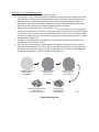
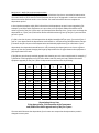
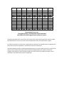
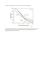
IC Cost and Price Model User Manual IC Knowledge LLC, PO Box 20, Georgetown, MA 01833 Tx: (978) 352 – 7610, Fx: (978) 352 – 3870, email: [email protected] Version 2015 model Introduction This manual presents an overview of IC Cost and Price Model and the basic workings of the model. Model description The IC Cost and Price Model is designed to easily calculate the cost and price of most low power silicon ICs. Examples of low power ICs include microcontrollers, microprocessors, FPGAs, low power ASICs, DRAM, Flash, SRAM, etc. The model does not cover any non‐silicon based ICs and does not cover power ICs or discrete devices; these are both covered by separate models. The IC Cost and Price model processes are limited to low power processes such as CMOS, BiCMOS, RFCMOS, DRAM, NAND, NOR, SRAM, etc. There is currently some BCD process coverage in the model but this will be removed as of January 1, 2016. BCD coverage is provided by our Discrete and Power Products Cost and Price Model. Specialized power IC and discrete device packages are also not covered by the IC Cost and Price Model. Power packages are covered in our Discrete and Power Products Cost and Price Model. The IC Cost and Price Model is also limited to past and current processes and processes expected to be introduced to production within the next year. Nodes not expected to be introduced in the next year are covered in our Strategic Cost Model that covers logic processes out to the 5nm node and memory processes out to the 12nm node. The IC Cost and Price Model provides some approximate values for equipment and materials requirements but for exact and detailed equipment and materials requirements the Strategic Cost Model should be utilized. Please note that our cost models are cost of goods sold (COGS) models and do not include below the line costs such as research and development (R&D) or selling, general and administration costs (SG&A). Our pricing calculations are cost plus gross margin (GM). R&D and SG&A costs are absorbed in GM as well as profits. Support and updates As a licensee to the IC Cost and Price Model you will receive all updates made to the model for twelve months from the date of purchase emailed to your email address of record. If you change your email address it is your responsibility to notify us. Free phone and email support will be provided for twelve months from the date of purchase of the model. On‐site or other forms of support are not provided. Model conventions There are several conventions used throughput the model. The gray areas on each model sheet contain the model inputs and outputs. The inputs that can be directly changed by the user are white areas within the gray, the gray areas are labels and model driven outputs and cannot be directly changed by the user. Throughout the model there are red dots indicating comments. Moving the cursor over the red dots displays information explaining input or outputs. In this manual, regular, bold and underlined text describe the model and model features. Italic text provides background on the inner workings of the model. Worksheet overview The following is a brief description of the model worksheets and the purpose of each sheet. The sheet tabs are color coded, gray is informational (these sheets may in some cases be editable but do not drive the model results), red are the main drivers (these sheets are editable), brown are results (these sheets are not editable), blue modifies the processes or performs comparisons or calculations (these sheets are editable). License (Gray tab) – the model software license. This sheet is not editable. Introduction (Gray tab) – a brief introduction to IC Knowledge and our cost modeling product line as well as disclaimer and warrantee information. This sheet is not editable. HELP (Gray tab) – a listing of the various ways to get help with the model. This sheet is not editable. Main Selections (red tab) – the 8 selections required to build a model are on this sheet. This is the main driver of model results. This sheet is user editable. Defaults (red tab) – this sheet displays the default values for all of the model defaults and allows the user to override them. This sheet is user editable. Cost Summary (brown tab) – the main summary of the cost model results including wafer, test and packaging cost. This sheet is not user editable. Lookups (gray tab) – lookup tables to help the user make selections on the ‘Main Selections’ tab. This sheet is user editable. Errors (gray tab) – this sheet provides details about any errors that occur in the model. This sheet is not user editable. Process adders (blue tab) – allows the user to add various process blocks to the base process. This sheet is user editable. Multiple die (blue tab) – this worksheet allows costs for multiple die in a single package to be calculated. This sheet is user editable. Wafer Fab Cost Detail (brown tab) – this worksheet displays detailed information about the wafer cost. This sheet is not user editable. Scenarios (blue tab) – this sheet allows the user to compare current model results to previous model results. This sheet is user editable. Revision History (Gray tab) – this worksheet displays the revisions made to the current year’s model along with details of what the changes were. This sheet is not user editable. Blank 1 (gray tab) ‐ an unlocked worksheet for user calculations and note. This sheet is user editable. Blank 2 (gray tab) ‐ an unlocked worksheet for user calculations and note. This sheet is user editable. Blank 3 (gray tab) ‐ an unlocked worksheet for user calculations and note. This sheet is user editable. Lists (gray tab) – lists of the numeric values that correspond to each model input setting. These values are useful when driving the model from the ‘Override’ worksheet. This sheet is user editable. Override (red tab) – this worksheet allows the user to drive the model from their own calculations. This sheet is user editable. Detailed worksheet descriptions In this section the “active” worksheets are described in more detail. Worksheet such as ‘License’, ‘Introduction’, ‘Help’, ‘Revision History’, ‘Lists’ and the blank worksheets are expected to be self‐ explanatory. Background – The IC Manufacturing Flow The following are the main steps in the IC manufacturing flow: Starting wafer – this is purchased by all IC manufacturers. Wafers come in a variety of sizes and types. When you select a process the appropriate wafer size and type is automatically selected. Wafer fabrication – anywhere between tens to tens of thousands of integrated circuits are fabricated on the surface of the wafer. The wafer yield is the number of wafers that complete fabrication process divided by the number of wafers started into the fab. Wafer sort (also called wafer test or wafer probe) – the ICs on the wafer surface are tested and the bad ICs are mark with an ink dot or in an electronic map so they won’t be packaged. Die yield is the number of die that pass wafer sort divided by the total number of die on the wafer. Wafer sort may be a single pass test or may include multiple passes at different temperatures, or before and after bakes and burn‐ins. Packaging – the individual ICs on the wafer are cut up and put into protective packages that provide electrical connections to the IC. Class test (also called final test) – the packaged ICs are tested to insure the ICs were correctly packaged without damage. For some ICs they can’t be fully tested until they are packaged and this may be the first full test. Class test may be a single pass test or may include multiple passes at different temperatures, or before and after bakes and burn‐ins. 1) Starting substrate silicon wafer (purchased). 2) Wafer fabrication fabricate IC’s on the wafer 4) Packaging assemble IC’s into packages 5) Mark & class/final test mark and final test packaged product IC Manufacturing Flow 3) Wafer sort/test test each IC, mark bad IC’s 14003 Main Selections (red tab) This is the main sheet driving the model. At the top of the sheet (row 7) next to the words “Main inputs (you must select all of these)” is a box that displays error messages if an error occurs. If an error message appears here please go to the ‘Errors’ sheet to learn more about the error. If an error is present you do not have a valid model and the error must be fixed. The most common error is to select a process that isn’t on‐line yet on the date selected in the ‘1 Select year and quarter to model’. If that is the error message, simply select a later date to model until the error message goes away. Other errors will require you to contact IC Knowledge to get them resolved. Row 8 has a box that will display an informational message if any defaults are overridden or any process adders are in use. This is not an error message but rather just information to make sure you don’t have a default overridden or a process adder active without realizing it. 1. Select year and quarter to model (cell D9) – this should be when the parts were made or when you expect them to be made if you want to project cost and price over time. The year and quarter affect depreciation (described further later in the manual), labor and utility rates, die yield, package cost, and material costs. 2. Select process to model (cell D11) – this is the most fundamental selection in the model and drives the process, the wafer fab the process is run in, labor and material costs and many other factors. The resulting wafer cost will be displayed in cell K11. An example of a process is: 300mm – 28nm – TSMC – HP (G) – CMOS – DGO, HKMG – 1P/11Cu. The nomenclature is wafer size (300mm) – node (28nm) – company (TSMC) – process name (HP (G)) – process type (CMOS) – process details (DGO, HKMG) – poly/metal layers and type (1P/11Cu). For a process where any of the entries don’t apply NA is used for not applicable. The abbreviations used in the process list are: Process Type BCD = Bipolar, CMOS and DMOS – being removed on 1/1/2016 BCD SOI = Bipolar, CMOS and DMOS on SOI – being removed on 1/1/2016 BiCMOS = Bipolar and CMOS BiCMOS SOI = Bipolar and CMOS on SOI Bipolar = Bipolar CMOS = Complimentary Metal Oxide Semiconductor DRAM = Dynamic Randon Access Memory EEPROM = Electrically Erasable Programable Read Only Memory FDSOI = Fully Depelted Silicon On Insulator ImgSen = Image Sensor InterPos = Interposer MG = Multi‐Gate (FinFET or TriGate) NAND = NAND Flash Memory NMOS = N type Metal Oxide Semiconductor NOR = NOR Flash Memory PDSOI = Partially Depeleted Silicon On Insulator SiGe = Silicon Germanium SRAM = Static Random Access Memory Process details 100V = 100 volts 20V DMOS = 20 volts Double Diffused Metal Oxide Semiconductor 30V = 30 volts 30V DMOS = 30 volts Double Diffused Metal Oxide Semiconductor 40V DMOS = 40 volts Double Diffused Metal Oxide Semiconductor 500V DMOS = 500 volts Double Diffused Metal Oxide Semiconductor 5Vts = 5 threshold voltages 60V = 60 volts 60V DMOS = 60 volts Double Diffused Metal Oxide Semiconductor 650V DMOS = 650 volts Double Diffused Metal Oxide Semiconductor 65V DMOS = 65 volts Double Diffused Metal Oxide Semiconductor 80V = 80 volts 80V DMOS = 80 volts Double Diffused Metal Oxide Semiconductor Analog = Analog BSI = Backside Image Sensor Comp = Complimemtary CPA = Common Platform Alliance DGO = Dual gate oxide DMOS = Double Diffused Metal Oxide Semiconductor DNW = Deep N‐Well eDRAM = Embedded Dynamic Random Access Memory eFlash = Embedded Flash Memory FPGA = Field Programmable Gate Array FSI = Front Side Illuminated Image Sensor Fuse = Fuse Ge PMOS = Germanium P Type Metal Oxide Semiconductor HfO/AlO = Hafnium Oxide/Aluminum Oxide High‐K Dielectric HKMG = High‐k metal gate HKMIM = High‐K Metal ‐Insulator‐Metal Capacitor HV = High Voltage LV = Low Voltage MIM = Metal‐Insulator‐Metal Capacitor Mixed Sig = Mixed Signal NMOS = N Type Metal Oxide Semiconductor PMOS = P Type Metal Oxide Semiconductor PPCaps = Polysilicon to Polysilicon capacitors Pressure Sensor = Pressure Sensor RCAT = Recessed Access Array Transistor RDL = Redistribution Layer RF = Radio Frequency Saddle Fin = Saddle FinFET Access Array Transistor Schottky = Schotty diode Schottky, TFR = Thin Film resistor SiGe = Silicon Germanium Silk ILD = A Low‐K Spin‐On Interlevel Dielectric TaN Res = Tantulum Nitirde Resistor TGO = Triple Gate Oxide TSV – Through Silicon Via VNPN = Vertical P‐Type/N‐Type/P‐Type Bipolar Transistor ZAZ = Zirconium Oxide/Aluminum Oxide/Zirconium Oxide High‐K Dielectric If you aren’t sure what to select for the process you can contact us and we will try to help. Generally most suppliers will disclose the node, wafer size, and metal and poly layers. The supplier may or may not disclose additional details but it never hurts to ask. The more information you have the more accurate the model will be. If you need a process that is not currently supported in the model you can request our “add a process to the model form” and fill that out. As long as the requested process fits within the model description from page one and we have enough information we will add the process to the model. Foundry volumes and margin There are basically three kinds of companies in the semiconductor business: Integrated Device Manufacturer (IDM) – IDM’s design their own products, fabricate the wafers, test them, package the parts, test them again and take them to market. Fabless – fabless companies design semiconductors but rely on other companies to fabricate the parts for them. They may or may not test the parts themselves and they typically outsource the packaging as well. Foundry – a company that owns their own wafer fabs and fabricates wafers for others. If the process you select is an IDM process (the company in the process description is an IDM) then the foundry margin will be zero. This is because the company transfers the fabricated wafers internally and only takes a margin at the end when the finished part is sold. If you select a foundry process (the company in the process is a foundry) then the foundry will sell the wafers to the fabless semiconductor company with a margin added to it (some IDMs also buy at least part of their wafer requirement from foundries). The cost to make a wafer depends on the process, the wafer fab and how full the fab is. Unless a customer is so big that they largely determine how full a fab is the wafer cost is not sensitive to the customer volume, however, the margin is very sensitive to volume. The table (row 14) lists the volumes in 200mm wafer equivalents a company has to buy from the foundry to be a low, medium or high volume customer of the foundry. This should reflect the total volume of wafers the company buys from the foundry, not just what they buy for a single product. Below the volume line the foundry margins in percentage are shown (row 15). Below this is a selection: 2a Select a foundry margin (cell D17) – if you select engineering the engineering margin will be added to the wafer cost, is you select low, average or high, the low average or high volume margin will be added to the cost. You can also directly choose a margin. If a non‐foundry process has been chosen the margins are zero unless you directly select a margin. The resulting wafer price (cost + margin) is displayed in cell K17. If you are not sure what to select for margin, there is a foundry usage and margin lookup on the ‘Lookups’ sheet. 3. Enter the die size – in cells D19 and F19 the die length and width in millimeters should be entered. The model takes the die size, adds street width and calculates the exact number of whole die that will fit onto a wafer based on wafer size and edge exclusion. There is more than one way to describe die size and it is important to understand the differences. The following figure illustrates three die in a row on a wafer. Notice that there is the physical die size and then between each die there is a blank “street”. The street provides an area for the saw cut used to separate the finished die. The model assumes that the die size that is entered is the physical die size of the die and by default the model adds a 75 micron street width when calculating the whole die on a wafer. Sometimes die sizes are specified using the stepping distance from the middle of a street to the middle of the next street. In this case you need to override the street width and set it to zero. Another situation that you may encounter is where a die size is measured after sawing, you need to make sure the measurement is the die only and not some remnant of the street still attached to the side of the die. The street is made wider than a typical saw cut to leave some room for misalignment and saw damage around the cut. Die Size Other factors to take into when determining the number of whole die on a wafer are the edge exclusion and die clustering. Edge Exclusion – due to issues with maintaining prefect process uniformity all the way to the edge of a wafer there is an edge exclusion area at the edge of the die where no good die exist. By default the model leaves a 2mm edge exclusion but you can override that if necessary on the ‘Defaults’ sheet. Die Clustering – virtually all fabs use stepper based exposure systems to print the patterns that build up ICs. The field of a stepper typically encompasses several die and then the field is stepped across the wafers. For gross die calculations it may be necessary to consider die clustering because the stepper field behaves like a big die with several die inside it. On the ‘Defaults’ sheet you can select various stepper (and scanner) field sizes to activate die clustering. 4. Select product type for test (cell D21) – the product type determines default test times and the type and cost for the test equipment. Many standard product types are pre‐defined here. In 5. 6. 7. 8. order to determine what test product type to select see the background section on Product Type Selection later in this manual. Enter the package pins (cell D23) – enter the number of pins on the package. This is used to help determine the equipment required for wafer sort and class test plus feeds into the package cost calculations. If the package has balls or pads instead of pins merely substitute the number of balls or pads. If the product is a bare die use the number of bond pads. For selected mainstream products there is a packaging type lookup on the ‘Lookups’ sheet that also lists pins. Select package type (cell D25) – from the dropdown list select the desired package type. For wafer scale packaging backgrind only, bumped die and bumped die with coating are supported. All of the major package types are also supported. We are often asked what to select for Chip Scale Packages (CSP), all CSP means is the the package is roughly the size of the die, it does not specify the actual package. A small BGA is a CSP, a small LGA is a CSP, etc. Simply select the correct package. For some package etypes such as BGA, LGA and PGA the package type can be preceded by a p for plastic, c for ceramic or a fc for flip chip. No packaging, reconstructed wafer and saw only are also supported for products such as image sensors. For selected mainstream products there is a packaging type lookup on the ‘Lookups’ sheet. Select packaging volume (cell D27) – the packaging volume is the total dollar volume the company the makes the IC does with the packaging house. This affects the packaging cost. For large IDMs this setting should generally be set to very high. Select package layers (cell D29) – only certain package types have layers such as BGA, LGA, and PGA. The box at cell F29 will tell you whether layers are active or not. If layers are inactive it does not matter what is selected fro layers. If layers are active, the more layers there are in the package the higher the package cost. Packages such as BGA, LGA and PGA start with a multilayer substrate similar to a PC board that the die is mounted down to. The substrate cost depends on the number of layers. For selected mainstream products there is a packaging type lookup on the ‘Lookups’ sheet that also lists layers. Background – Cost Accounting Cost accounting practices break out manufacturing costs in three categories: 1. Material – material only includes materials that become part of the final product that is shipped. Materials consumed in product are included in overhead and do not count as materials. 2. Labor – labor only include direct or “touch” labor, basically the operators who make the product. Indirect labor such as engineers, technicians, managers and supervisors are included in overhead. 3. Overhead – everything else. The following table summarizes what is included in each category for different phases of IC production. Category Wafer Fabrication Packaging Test Material Starting Wafer Substrates, Leadframes, None Wire, Mold Compound Labor Operators Operators Operators Depreciation, Depreciation, Overhead Depreciation, Equipment Equipment Equipment maintenance, Indirect maintenance, Indirect maintenance, Indirect labor, Facilities costs, labor, Facilities costs, labor, Monitor wafers, Consumables Consumables Facilities costs, Consumables Background ‐ Wafer Cost Calculation As previously described, cost accounting practices break up the cost to manufacture a product for sale into three categories, material, labor and overhead: Material – material is confined to materials used to make the product that becomes part of the product that is shipped. Only if the material becomes a physical part of the product being shipped does it count in the material category. For wafer fabrication the only material is the starting wafer. Labor – labor in this case is restricted to direct labor sometimes referred to as touch labor. Direct labor is the labor cost for the operators who physically manufacture the product. Engineers, supervisors, technicians and managers do not count as direct labor and are included in the indirect labor category described below. Overhead – everything else required manufacturing the product. In the IC Knowledge cost models overhead is broken down into depreciation, equipment maintenance, monitor wafers, indirect labor, facilities and consumables. As previously described overhead is everything other than material (starting wafers) and labor (direct labor from operators) required to produce the product. The following is a further breakout and discussion of the various overhead sub categories: Depreciation – equipment has a finite usable lifetime. The idea behind depreciation is to take the cost of a piece of equipment and write it off over the course of its useful life. For example if a piece of equipment costs one million dollar and has a useful lifetime of five years, two hundred thousand dollars would be charged to manufacturing cost each year for each of the first five years. In the semiconductor industry the useful life of some process equipment may be shorter than government regulations allow and furthermore regulations vary from country to country. Generally speaking the industry has settled on five year depreciation for process equipment when reporting results (although other rules may be used for tax purposes). The following are the default depreciation rates used in the cost models: Item Process tools Process tools installation Building systems (ultrapure water, gas and chemicals, cleanroom, HVAC) Automation Building structure Useful life 5 years 5 years Depreciation rate 20% 20% 10 years 10% 10 years 15 years 10% 7% The deprecation calculation is the cost of the item multiplied by the depreciation rate. This amount is charged to the manufacturing cost each year until the useful life is reached at which time the depreciation for that items goes to zero. With expansions and upgrades there may be a wide variety of equipment ages in the same facility. The Cost Model provides for an initial equipment set and up to three upgrades/expansions and tracks each set individually. Equipment Maintenance – the cost of parts and service contracts for the process equipment are captured in this category. The company employees such as technicians and engineers that maintain the equipment are not counted in this category. Equipment maintenance is calculated as a percentage of the original acquisition cost of the equipment used to estimate yearly maintenance costs. Indirect labor – engineers (both process and equipment), technicians (both process and equipment), supervisors and managers are all counted in this category. Indirect labor hour per mask layer are used to estimate total indirect labor hours. Total indirect labor hour are then broken down by type using “typical” fab indirect labor profiles and labor rates for engineers, technicians, supervisors and managers by country are used to calculate indirect labor costs. Monitor wafers – test wafers used to monitor the performance of equipment. These wafers are used to perform a test by running them through one or more process steps and then measuring the result. The wafers are then scrapped or reclaimed. Facilities – the cost of utilities (electricity, natural gas and water), ultrapure water generation, waste water treatment, facility maintenance (HVAC, Ultrapure water, gas and chemical systems), insurance, occupancy (cleaning and waste disposal), landscaping and telecommunications. Consumables – reticles, photochemicals, cleaning chemicals, etching and deposition gases, bulk gases, CMP pads and slurries, sputter targets, implant sources, deposition precursors, etc. Background – Wafer fab equipment depreciation Due to the complexity of the wafer fab equipment calculations they bear a more detailed examination. The model allows a fab to have an initial equipment set and up to 10 upgrades. In each case when and what came online and how much it cost is tracked. The model also allows the user to adjust the depreciation period. In the simplest example a wafer fab is built with an initial equipment set and is never upgraded. If for example a one billion dollar equipment set is put online, then by default $200 million dollars will be written off each of the first 5 years and in year 6 depreciation becomes zero. If a user were to change the depreciation to 7 years, then $143 million dollars would be written off each of the first 7 years and then go to 0 in year 8. If a fab is less than 6 years, old the depreciation be default would be 20% per year, if you switch from 5 year to 7 year depreciation the depreciation would switch to ~14% decreasing the depreciation charges. If however the fab is 6 years old the depreciation would be 0 by default and if you switched to 7 year depreciation the depreciation would become ~14% increasing the depreciation cost. Once a sufficient amount of time has passed changing the length of depreciation has no effect because the equipment is fully depreciated in all cases. If the fab has gone through multiple upgrades the situation gets a lot more complicated. For example, if a fab had an initial equipment set of $1 billion dollars and then each year had a $100 million dollar equipment upgrade for the first 5 years the deprecation would look like the following. Initial Upgrade Upgrade Upgrade Upgrade Upgrade Total set 1 2 3 4 5 Year 1 $200M $0M $0M $0M $0M $0M $200M Year 2 $200M $20M $0M $0M $0M $0M $220M Year 3 $200M $20M $20M $0M $0M $0M $240M Year 4 $200M $20M $20M $20M $0M $0M $260M Year 5 $200M $20M $20M $20M $20M $0M $280M Year 6 $0M $20M $20M $20M $20M $20M $100M Year 7 $0M $0M $20M $20M $20M $20M $80M Year 8 $0M $0M $0M $20M $20M $20M $60M Year 9 $0M $0M $0M $0M $20M $20M $40M Year 10 $0M $0M $0M $0M $0M $20M $20M Year 11 $0M $0M $0M $0M $0M $0M $0M Year 12 $0M $0M $0M $0M $0M $0M $0M Year 13 $0M $0M $0M $0M $0M $0M $0M Depreciation Versus Year. 5 Year depreciation, $1 billion dollar initial investment and $100 million dollar upgrade each of the first 5 years. The next table illustrates the depreciation for the same case except that the depreciation period is changed to seven years. Year 1 Year 2 Year 3 Year 4 Year 5 Year 6 Year 7 Year 8 Year 9 Year 10 Year 11 Year 12 Year 13 Initial set $143M $143M $143M $143M $143M $143M $143M $0M $0M $0M $0M $0M $0M Upgrade Upgrade Upgrade Upgrade Upgrade 1 2 3 4 5 $0M $0M $0M $0M $0M $14M $0M $0M $0M $0M $14M $14M $0M $0M $0M $14M $14M $14M $0M $0M $14M $14M $14M $14M $0M $14M $14M $14M $14M $14M $14M $14M $14M $14M $14M $14M $14M $14M $14M $14M $0M $14M $14M $14M $14M $0M $0M $14M $14M $14M $0M $0M $0M $14M $14M $0M $0M $0M $0M $14M $0M $0M $0M $0M $0M Total $143M $157M $171M $186M $200M $214M $214M $71M $57M $43M $29M $14M $0M Depreciation Versus Year. 7 Year depreciation, $1 billion dollar initial investment and $100 million dollar upgrade each of the first 5 years. Comparing the tables we can see that for the first five years the five year depreciation results in higher total depreciation costs, then for years seven through twelve seven year depreciation is higher. In reality the situation is actually more complex than this with up to ten upgrades plus as upgrades take place some of the older equipment is removed and must be accounted for. The model handles all of this accounting automatically and it isn’t even visible to the user. If you feel you need to see the details of the equipment calculations and depreciation you need to purchase our strategic model where all of the calculation details are visible. We do not expose that detail in the IC model due to the audience the model is designed for. Background – Selecting Product Type The product type you select sets the defaults for test equipment cost, test times, parallel testing and many other factors. Please note you can manually set all of these value on the ‘Defaults’ tab and should if you know the specific values to use. If not selecting product type will provide reasonable defaults. The following is a check list presented in order to make product type selections: 1. For an ASIC product use the ASIC product type. To determine the performance and complexity of the ASIC product there is an ASIC product type lookup on the lookups page, select the value from that lookup from the ‘4 Select product type for test’ drop down. 2. If the product is a CMOS image sensor select CIS with the appropriate number of megapixels from the ‘4 Select product type for test’ drop down. 3. If the product is DRAM memory select the appropriate DRAM type and number of bits from the ‘4 Select product type for test’ drop down. 4. If the product is a digital signal processor (DSP) select DSP with the number of bits and cores from the ‘4 Select product type for test’ drop down. 5. If the product type is flash select the type (NAND or NOR) and number of bits from the ‘4 Select product type for test’ drop down. 6. If the product is a microcontroller select microcontroller with the appropriate number of bits, cores and flash memory from the ‘4 Select product type for test’ drop down. 7. If the product type is a microprocessor select microprocessors with the appropriate number of cores from the ‘4 Select product type for test’ drop down. 8. If the product type includes both analog and digital functions such as an analog to digital or digital to analog converter, select mixed signal very simple, simple, medium or complex from the ‘4 Select product type for test’ drop down. We do not currently have any help on what constitutes very simple, simple, medium or complex. 9. If the product type is an RF product, select RF very simple, simple, medium or complex from the ‘4 Select product type for test’ drop down. We do not currently have any help on what constitutes very simple, simple, medium or complex. 10. If the product type is an SRAM select SRAM and the appropriate number of bits from the ‘4 Select product type for test’ drop down. 11. For any product type not yet listed use the ASIC product type. To determine the performance and complexity of the product there is a lookup on the lookups page, select the value from that lookup from the ‘4 Select product type for test’ drop down. Defaults (red tab) The ‘Defaults’ sheet displays the default value for dozen of model setting and allows the user to override them. The default values are technology specific and many if not most user never need to adjust anything on this page. In general, column D displays default values, column E allows the user to override the default and column F displays the final value used. The ‘Defaults’ sheet is divided into sections by general area the defaults address. Wafer Fab – these are setting that effect the wafer fab cost calculations. Utilization ‐ The percentage of the fab capacity that is utilized. This has a huge effect on wafer cost with wafer cost going up as utilization goes down. The most common reason for changing this setting is described in the applications note “Using the IC Cost and Price Model to Estimate Foundry Wafer Cost and Price’ available on the IC Cost and Price Model page on our web site. By default the model is set to 90% utilization because that is the utilization typically assumed when setting price. Country ‐ The country the fab is located in. Changing the country changes the labor and utility rates. Capacity (wpm) – the is the capacity in wafers per month for the fab currently selected (the fab is determined by the process selected on the ‘Main Selections’ sheet. Wafer type – The starting wafer type. This is automatically filled in for the process selected on the ‘Main Selections’ sheet. Override values available include: o Polished ‐ a bare unprocessed wafer. o Epi, a polished wafer with an epitaxial layer on it. o PDSOI (partially depleted SOI), SOI used for some older technologies (typically 40nm and above). Please note that selecting PDSOI will change the starting wafer cost but not adjust the process to reflect the differences in SOI versus bulk processing. o FDSOI‐2D (fully depleted SOI) used for planar fully depleted SOI processes. Please note that selecting FDSOI‐2D will change the starting wafer cost but not adjust the process to reflect the differences in SOI versus bulk processing. o FDSOI‐3D (fully depleted SOI) used for some FinFET processes. Please note that selecting FDSOI‐3D will change the starting wafer cost but not adjust the process to reflect the differences in SOI versus bulk processing. Mask set pre‐paid – this setting determines whether the mask set cost is amortized into the wafer manufacturing cost. By default this is set to “No” for foundries and “Yes” for everything else. This is because mask sets are typically paid for as part of NRE for foundry processes and not included in the cost. You can override the vale to “No” for not amortized or “Yes” for amortized. Mask set usage (wafers/set) – sets the number of wafers a mask set is amortized over. This number depends on the product type and year. If ‘Mask set pre‐paid’ is yes, this setting has no effect. Wafer yield (%) – the number of wafers finished through the wafer fabrication process divided by the number of wafers introduced into the wafer fabrication process. The default yield is calculated based on the number of mask layers in the process. Years to depreciate equipment over – equipment is depreciated using a straight line calculation over the number of years set here, by default this is set to five years. For 5 years 1/5 of the equipment is written off for each of the first 5 years, for 7 years 1/7 of the equipment value is written off each year for 7 years, etc. See the background sections on “Wafer cost calculation” and “Wafer fab equipment depreciation” to better understand this setting. Wafer cost override – when set to “Default” (column F) the wafer cost calculated by the model is used. If set to “User” (column F) the value entered is used (column E). Equipment set cost multiplier – the equipment set cost is multiplied by this value. By default this is set to one. Gross and Net Die – these setting determine the number of whole die per wafer (gross die) and the number of good die after test (net die) Defect density (N/cm2) – the defects per unit area utilized to calculate the die yield (see the background on “Yield Models”). The high the defect density the lower the yield will be for a given die size. The default defect density depends on the process, year and quarter. Please note the default defect densities are for the Murphy model and if you select a different defect model you must enter your own defect density. Edge exclusion – wafer fabrication processes are not perfectly uniform to the wafer edge and there is an “exclusion” zone where no good die exist. This “edge exclusion” is subtracted from the wafer size to calculate the number of whole die that fit on the wafer. Die clustering – die are printed on the wafer using stepper systems where multiple die are printed at each time. This can cause the groups of die printed at the same time to behave like one large die instead of individual die when it comes to fitting the die on the wafer. Die clustering allows the user to set the die clustering so it is taken into account when calculating gross die. Street width – the area between die left empty to make a space for the wafer saw. See also “Die size” in the ‘Main Selections” sheet description. Yield model – the default yield model utilized to calculate the die yield is the murphy model. This setting allows the user to override the default yield model and select an alternative model. See the background on “Yield Models” following this section for a discussion of yield models. N for Bose Einstein – the Bose Einstein yield model requires a value for N to be entered. If you select Bose Einstein as the yield model in the previous setting you must enter N here. If any other model is selected this entry has no effect. See the background on “Yield Models” for more information. Die area breakout – this is a set of 8 setting that allows the user to calculate and use a defect density based on different defect densities for different areas of the die. The first four settings define the % of the die that is 3 different types of memory and logic. The sum of these four areas must be 100% or you will get an error. Changing these four setting doesn’t have any effect until you also change the defect densities for each of the 4 areas. By default the four areas all have the default defect density. You must go in and change this after you have selected the different area percentages. We do not have any data on defect densities for different memory areas and this is just a calculator for user convenience. You as a user are responsible for entering the areas and defect densities here. Test – this section sets all of the defaults for wafer sort and class test. Product level – this is a very useful setting for companies involved in automotive, military and aerospace. By default this is set to commercial, when you switch to automotive, military or aerospace additional testing and documentation is activated. Sort equipment date on‐line – the year the sort equipment came on‐line. This is used for the equipment depreciation calculation. The default value is set by the ‘2 Select process to model’ on the ‘Main Selections’ sheet. Sort test time (secs) – this is the time in seconds to test a single die. The default value is determined by the ‘4 Select product type for test’ setting on the ‘Main Selections’ sheet. If you know the actual test time you should select it here. Sort parallel testing (units) – the number of units tested at the same time during sort. The default depends on the ’1 Select year and quarter to model’ and ‘4 Select product type for test’ settings on the ‘Main Selections’ sheet. Sort parallel efficiency (%) – the efficiency of units tested at the same time during sort. The default depends on the ’1 Select year and quarter to model’ and ‘4 Select product type for test’ settings on the ‘Main Selections’ sheet. This is used along with the number of units sorted in parallel to determine the adjusted test time. See the background “Parallel testing efficiency” after this section. Sort system cost ($/system) – this is the default of the sort tester and prober calculated by the model based on the product being tested. Sort country – this is the default country wafer sort is performed in. By default it is the same country that the fab is in. Sort utilization (%) – this is the percent of the uptime sort equipment is being used to process wafers. The default depends on the ’1 Select year and quarter to model’ and ‘4 Select product type for test’ settings on the ‘Main Selections’ sheet. Sort uptime (%) – this is the percent of the time sort equipment is up and available to process wafers. The default depends on the ’1 Select year and quarter to model’ and ‘4 Select product type for test’ settings on the ‘Main Selections’ sheet. Sort 1 time (% of sort test time) – sort may require multiple passes. This setting is the percentage of the sort test time that is used to test the die during the first pass. For some devices this may be the only test and the test time would be 100%. For other products, there may be multiple passes and test 1 might be only a partial test. The default depends on the’1 Select year and quarter to model’ and ‘4 Select product type for test’ settings on the ‘Main Selections’ sheet and the “Product level”. Wafer bake – for certain products types the wafers are sorted, then baked to weed out infant mortality and sorted again. This setting sets the bake time. The default depends on the 1’1 Select year and quarter to model’ and ‘4 Select product type for test’ settings on the ‘Main Selections’ sheet and the “Product level”. Memory repair – for certain memory parts after sort 1 the extra memory bits can be sued to repair a defective memory array by blowing fuses. The default depends on the ’1 Select year and quarter to model’ and ‘4 Select product type for test’ settings on the ‘Main Selections’ sheet. Sort 2 time (% of sort test time) – sort may require multiple passes. This setting is the percentage of the sort test time that is used to test the die during the second pass. The default depends on the ’1 Select year and quarter to model’ and ‘4 Select product type for test’ settings on the ‘Main Selections’ sheet and the “Product level”. Sort 3 time (% of sort test time) – sort may require multiple passes. This setting is the percentage of the sort test time that is used to test the die during the third pass. The default depends on the ’1 Select year and quarter to model’ and ‘4 Select product type for test’ settings on the ‘Main Selections’ sheet and the “Product level”. Class equipment date on‐line – the year the class equipment came on‐line. This is used for the equipment depreciation calculation. The default value is set by the ‘2 Select process to model’ on the ‘Main Selections’ sheet. Class test time (secs) – this is the time in seconds to test a single part. The default value is determined by the ‘4 Select product type for test’ setting on the ‘Main Selections’ sheet. If you know the actual test time you should select it here. Class parallel testing (units) – the number of units tested at the same time during class test. The default depends on the ’1 Select year and quarter to model’ and ‘4 Select product type for test’ settings on the ‘Main Selections’ sheet. Class parallel efficiency (%) – the efficiency of units tested at the same time during class test. The default depends on the ’1 Select year and quarter to model’ and ‘4 Select product type for test’ settings on the ‘Main Selections’ sheet. This is used along with the number of units Classed in parallel to determine the adjusted test time. See the background “Parallel testing efficiency” after this section. Class system cost ($/system) – this is the default of the Class tester and handler cost calculated by the model based on the product being tested. Class test country – this is the default country wafer class test is performed in. By default it is the Philippines. Class test utilization (%) – this is the percent of the uptime class test equipment is being used to process wafers. The default depends on the 1’1 Select year and quarter to model’ and ‘4 Select product type for test’ settings on the ‘Main Selections’ sheet. Class test uptime (%) – this is the percent of the time class test equipment is up and available to process wafers. The default depends on the 1’1 Select year and quarter to model’ and ‘4 Select product type for test’ settings on the ‘Main Selections’ sheet. Class test yield – the percentage of units that pass class test. By default this is based on the product pins. Lot size – the number of parts in a lot. This setting only takes effect if the part is aerospace or military or you turn on one of the next eight settings, or final three settings: Internal visual ($), Non destructive bond pull ($), Serialization ($), Temp cycle ($), Constant acceleration ($), Particle impact noise ($), Fine and gross leak test ($), Radiographic ($), Fine and gross leak test ($), External visual inspection ($), Documents ($). Internal visual ($) – the cost per lot to perform internal visual inspection. The default depends on the ’1 Select year and quarter to model’ and ‘4 Select product type for test’ settings on the ‘Main Selections’ sheet and the “Product level”. Non‐destructive bond pull ($) – the cost per lot to perform bond pull strength testing, this is not done to failure but rather to a minimum pull strength. The default depends on the ’1 Select year and quarter to model’ and ‘4 Select product type for test’ settings on the ‘Main Selections’ sheet and the “Product level”. Serialization ($) – the cost per lot to serialize the parts. The default depends on the ’1 Select year and quarter to model’ and ‘4 Select product type for test’ settings on the ‘Main Selections’ sheet and the “Product level”. Temp cycle ($) – the cost per lot to perform temp cycling. The default depends on the ’1 Select year and quarter to model’ and ‘4 Select product type for test’ settings on the ‘Main Selections’ sheet and the “Product level”. Constant acceleration ($) – the cost per lot to perform constant acceleration testing. The default depends on the ’1 Select year and quarter to model’ and ‘4 Select product type for test’ settings on the ‘Main Selections’ sheet and the “Product level”. Particle impact noise ($) – the cost per lot to perform particle noise impact testing. The default depends on the ’1 Select year and quarter to model’ and ‘4 Select product type for test’ settings on the ‘Main Selections’ sheet and the “Product level”. Fine and gross leak test ($) – the cost per lot to perform fine and gross leak testing. The default depends on the ’1 Select year and quarter to model’ and ‘4 Select product type for test’ settings on the ‘Main Selections’ sheet and the “Product level”. Radiographic ($) – the cost per lot to perform radiographic testing. The default depends on the ’1 Select year and quarter to model’ and ‘4 Select product type for test’ settings on the ‘Main Selections’ sheet and the “Product level”. Pre burn‐in test time (% of class test time) – Class test may require multiple passes. This setting is the percentage of the class test time that is used to test the product before burn‐in. For some devices this may be the only test and the test time would be 100%. For other products, there may be multiple passes and this might only be a partial test. The default depends on the ’1 Select year and quarter to model’ and ‘4 Select product type for test’ settings on the ‘Main Selections’ sheet and the “Product level”. Burn‐in (hrs) – the number of hours the product is burned‐in to weed out infant mortality. The default depends on the ’1 Select year and quarter to model’ and ‘4 Select product type for test’ settings on the ‘Main Selections’ sheet and the “Product level”. Interim electrical (% of class test time) – Class test may require multiple passes. This setting is the percentage of the class test time that is used to test the product in between multiple burn‐ ins. The default depends on the ’1 Select year and quarter to model’ and ‘4 Select product type for test’ settings on the ‘Main Selections’ sheet and the “Product level”. Burn‐in (hrs) – the number of hours the product is burned‐in to weed out infant mortality. This is a second burn‐in. The default depends on the ’1 Select year and quarter to model’ and ‘4 Select product type for test’ settings on the ‘Main Selections’ sheet and the “Product level”. Room test (% of class test time) – Class test may require multiple passes. This setting is the percentage of the class test time that is used to test the product at room temperature after burn‐in(s). The default depends on the ’1 Select year and quarter to model’ and ‘4 Select product type for test’ settings on the ‘Main Selections’ sheet and the “Product level”. Hot test (% of class test time) – Class test may require multiple passes. This setting is the percentage of the class test time that is used to test the product at high temperature after burn‐ in(s). The default depends on the ’1 Select year and quarter to model’ and ‘4 Select product type for test’ settings on the ‘Main Selections’ sheet and the “Product level”. Cold test (% of class test time) – Class test may require multiple passes. This setting is the percentage of the class test time that is used to test the product at cold temperature after burn‐ in(s). The default depends on the ’1 Select year and quarter to model’ and ‘4 Select product type for test’ settings on the ‘Main Selections’ sheet and the “Product level”. Fine and gross leak test ($) – the cost per lot to perform fine and gross leak test. The default depends on the ’1 Select year and quarter to model’ and ‘4 Select product type for test’ settings on the ‘Main Selections’ sheet and the “Product level”. External visual inspection ($) – the cost per lot to perform external visual inspection. The default depends on the ’1 Select year and quarter to model’ and ‘4 Select product type for test’ settings on the ‘Main Selections’ sheet and the “Product level”. Documents ($) – the cost per lot for dosuments. The default depends on the ’1 Select year and quarter to model’ and ‘4 Select product type for test’ settings on the ‘Main Selections’ sheet and the “Product level”. Assembly and Packaging – default settings for assembly and packaging Assembly yield – the percentage of parts completed through assembly divided by the parts started into assembly. The default is calculated based on the number of pins. Packaging source – some IDMs do their own packaging. By default this is set to out‐sourced but if you switch this to internal the margin is removed from the cost. Backgrind – determines whether the wafer is background before assembly. The default depends on the ‘6 Select package type’ setting on the ‘Main selections’ sheet. Copper wire bonds – the default is gold wire bonds but copper wire bonds are becoming a common lower cost option. Resistors/capacitors (#) – some products have resistors and or capacitors included in the package. Select the total number of resistors and capacitors here. Exposed pad/heat slug – for certain higher power packages an exposed heat pad or heat slug is used to improve heat dissipation. This setting is no by default. Package cost override – by default (default in column F) the calculated packaging cost is sued in the model. If you select “User” (column F), then the user entered value (column E) is used. Background – Yield Models Yield models are based on a simple concept that there are a specific number of random defects on each wafer that can cause a die to fail test. The higher the defect density but also the larger the die 9see the figure) Defect Density and Yield As you can see from the figure, for an identical pattern and number of defects the yield is lower for larger die. This concept is mathematically expressed by defect models described below. The model supports Bose‐Einstein, Exponential, Murphy, Poisson and Seeds Yield models. The mathematics and resulting yields for each model are: Bose‐Einstein 1 1 Exponential 1 1 Murphy 1 Poisson Seeds √ Where: A is the area, D is the defect density and N is the number of mask layers. A comparison of the models for a value of D=1.0 is shown in the following figure: Please note that the model default is the Murphy Model and all of the default defect densities are based on a Murphy Model. If you switch the model used you must enter your own defect density that is appropriate for the model you have chosen. Background ‐ Parallel testing efficacy Testing multiple devices in parallel is an important technique for reducing test costs by spreading expensive test hardware costs out over more units. However, the more units tested in parallel the longer the test time characterized by the test efficiency given by the following formula. 1 1 Where T1 is the time to test one unit, N is the number of units tested in parallel and TN is the test time for N units. The ITRS has defined M and N by product and by year and we use those values to calculate the test time in parallel based on our estimates of T1. Background – Test and Burn‐In Usage Testing of integrated circuits is typically performed at wafer level as wafer sort or probe and at product levels as class or final test. At wafer sort testing is typically single pass testing with the exception of Flash where testing is done followed by wafer bake and then a second testing pass. The two testing passes enable the number of units that went bad during wafer bake to be calculated. Automotive product testing may require multiple tests at different temperature, for example hot, cold and room temperature. For automotive multiple temperature testing in sort would be for die that will be used as flip chips in modules or other die used directly. If the die will go through the normal packaging process, then multiple temperature testing would likely be deferred until class test. At class test products are typically tested, burned‐in and tested again with the exception of lower end parts that are single pass tested with no burn‐in. Automotive parts may once again be tested hot, cold and at room temperature. Aerospace and Military add additional test and inspections. Background ‐ Parallel testing efficacy Testing multiple devices in parallel is an important technique for reducing test costs by spreading expensive test hardware costs out over more units. However, the more units tested in parallel the longer the test time characterized by the test efficiency given by the following formula. 1 1 Where T1 is the time to test one unit, N is the number of units tested in parallel and TN is the test time for N units. The ITRS has defined M and N by product and by year and we use those values to calculate the test time in parallel based on our estimates of T1. Cost Summary (brown tab) The cost summary sheet summarizes all of the cost results from the model. This page is not user editable except a few white areas where previous results can be pasted for comparison purposes. General information Rows 8 through 15 display information related to the wafer fab and model. The date to model and current process are from the ‘1 Select year and quarter to model’ and ‘2 Select process to model’ selections on the ‘Main Selections’ sheet. The masks, fab name, fab on‐line and process on‐line dates, country and capacity are all the defaults for the fab associated with the ‘2 Select process to model’. The utilization is 90% by default unless overridden on the ‘Defaults’ sheet. Cell F15 also displays an information message if any defaults have been overridden. Wafer Cost Rows 18 through 28 break out the wafer fabrication cost into the major cost categories (see background Wafer Cost Calculation for more information). Column C lists the categories, column D has the annual costs for the entire fab in millions of dollars, column E has the costs in dollars per wafer, column F has the percentage of the total for each category, column G allows the user to paste results for comparison purposes. This is useful for understanding what the differences in costs are between two processes. You paste the results from one process, then select a different process and you can compare the cost by category between the two to understand what is different. Column H presents the results in dollars per square centimeter, column I presents the costs in dollars per mask and finally in column J the blended average depreciation rate for all of the different equipment sets is displayed (see background Wafer fab equipment depreciation). Process adders Rows 31 through 50 indicate whether any process adders are active and if so which ones. There is also a pie chart of the wafer cost by category. Wafer selling price In rows 53 and 54 the foundry gross margin percentage (if any), foundry margin dollars (if any) and resulting selling prices (wafer cost plus foundry margin) are displayed. General information In rows 57 and 58 the product type and die size are displayed. Die cost Rows 61 through 66 display the die cost elements. The gross ide per wafer, die yield in percentage, net die per wafer (gross die multiplied by die yield), wafer sort cost, tested wafer cost (wafer selling price plus wafer sort cost) and cost per good tested die (tested wafer cost divided by net die) and all displayed in column D. Column E has an area where you can paste or enter value to compare too. Product information Row 69 displays the package type and number of package pins. Product cost Rows 72 through 77 display the product cost. The assembly yield, package and assembly cost, packaged die cost, class test cost, class test yield and product cost are all displayed in column D. Column E has an area where you can paste or enter value to compare too. The background ‘Product cost calculation’ following this section explains the calculations. Selling price Rows 84 through 98 display the selling price of the product versus margin and also present a pie chart breaking out product cost into major categories by percentage. The ‘Background – Gross Margin‘ and ‘Background – Cost and Price’ following this section have information on gross margin. There is also a ‘Gross Margin; lookup on the ‘Lookups’ tab. Background – Product Cost Calculation The product cost calculations are made as follows: The packaged die cost calculation is by default based on packaging being performed by an outside contractor (this default may be changed on the ‘Defaults’ worksheet. When an outside contractor is used the contractor is only paid for good packages. Packaged die cost = cost per tested good die/packaging yield + package cost If the default is changed to in‐house packaging then: Packaged die cost = (cost per tested good die + package cost)/packaging yield Product cost is calculated by: Product cost = (packaged die cost + class test cost)/class test yield Background – Gross Margin Gross margin is the selling price minus the cost of goods sold. Gross margin percentage is the gross margin divided by the selling price for example: If a product has a cost of goods sold (COGS) of $0.70 and sells for $1.00, then the gross margin (GM) is $0.30 making the gross margin 30%. To convert from COGS to selling price for a given GM% use the following: GM% Divisor 20% 0.80 30% 0.70 40% 0.60 50% 0.50 60% 0.40 70% 0.30 For example, if COGS is $1.40, then a 60% GM would give a selling price of $3.50. A number of our customers have incorrectly made these calculations. Background – Cost and Price Cost is what it costs to make a product; price is what the market is willing to pay for the product. If you produce and sell a product the hope is always that the price will be greater than the cost by a significant margin but this is not always that case. Profit is gross margin minus below the line costs such as research and development, and general, selling and administrative Gross margins need to typically be greater than the high teens percentage to actually make a profit. Price = cost + gross margin If the cost is known (and that is primarily what this model calculates) and gross margin is known or can be estimated, then selling pricing is known and or can be estimated. Lookups (gray tab) The lookups sheet provides six lookups to help determine what value to use elsewhere in the model. The lookups page suggests values to use but doesn’t drive the model results. Foundry usage Select a company and node from the dropdown and the foundry used, comments, and foundry volume are displayed. This lookup helps with ‘2 Select a process to model’ and the ‘2a Select a foundry margin’ selections on the ‘Main Selections’ sheet. Die size Select the company and product from the dropdown and the die size is displayed. This lookup helps with the ‘3 Enter the die size’ entry on the ‘Main Selections’ sheet. ASIC test type This lookup gives a rough idea of what ASIC test type to select in the ‘4 Select product type for test’ dropdown on the ‘Main Selections’ sheet. You select the node and also select a die area that is the next larger size than your die. For example, if you die is 100mm2, then it is bigger than 64mm2 and smaller than 128mm2 so you pick 128mm2. Package type This lookup helps with ‘5 Enter the number of package pins’, ‘6 Select package type’ and ‘8 Select package layers’ on the ‘Main Selections’ sheet. Select the company and product type from the dropdown and the package type, package pins and layers are displayed. Gross margin Select a company from the dropdown and the companies average gross margin is displayed for the last 5 years and a 5 year average is also displayed. Selling price This is a calculator for selling price. The product cost calculated by the model is automatically filled in, you can then enter a gross margin and a selling price is displayed. You can also enter a product price and volume and have a price volume curve displayed. This is useful for example if you go on a distributor site and get a one thousand (1k) piece price, you can enter that price and see what the price will be at higher volumes. Errors (gray tab) In the event of an error in the model the type of error is displayed on this sheet. If the error is “The wafer fab doesn’t exist yet” simply select a later date on the ‘1 Select the year and quarter to model’ selection on the ‘Main Selections’ sheet. Generally speaking all other errors will require you to notify IC Knowledge so that we can fix the error. Process Adders (blue tab) The ‘Process Adders’ tab allows the user to modify a base process to include additional features. Al bond pads (yes/no) – adds an aluminum bond pads for wire bonding of copper metallization. Dual strain layers (yes/no) – adds dual strain layers. Embedded DRAM (stacked cell) (yes/no) – adds a stacked DRAM embedded DRAM. Embedded Flash (ST Micro type ‐ >40nm) (+10 masks, +1 poly) (yes/no) – adds an embedded Flash process similar to one ST Micro uses. This can be added to any process but is most relevant between 40nm and 130nm. Embedded Flash (SST SuperFlash ESF2 ‐ 110nm to 250nm) (+9 masks, +3 polys) (yes/no) – adds SST SuperFlash ESF2 to a process. ESF2 is most relevant between 110nm and 250nm. Embedded Flash (SST SuperFlash ESF3 ‐ <110nm) (+11 masks, +4 polys) (yes/no) – adds SST SuperFlash ESF3 to a process. ESF3 is most relevant below 110nm. Extension/halo implant (additional) – adds additional extension/halo masks and implants. Fuse (yes/no) – adds a fuse typically used for memory repair. High resistance poly resistor (yes/no) –adds a high resistance polysilicon resistor. This is a common adder for analog processes. High speed SiGe NPN (yes/no) – add a high speed silicon germanium NPN transistor to the process. This is commonly used in very high performance RF processes. Masked gate oxides (additional) – adds additional gate oxides. This block uses a mask to etch away gate oxide in a localized area and grow and additional thickness. You can 1 or 2 additional gate oxides. Metal layers (additional) – adds additional metals layers. You can add 1 to 4 additional metal layers. MIM Capacitors (yes/no) – adds an MIM capacitor. MIM caps are common in analog and RF processes. Raised Source/Drain ‐ (additional) – adds raised source/drains. You can add 1 or 2. Source/Drain contact (additional) – adds additional source drain masks and implants. You can 1 to 4. Stress memorization (yes/no) – add stress memorization. Thin film resistors (yes/no) – adds thin film resistors. This add on is most commonly used in analog or RF applications. Through silicon via (yes/no) – adds a via middle through silicon via to the process. Vt adjust (additional) – adds Vt adjust masks and implants to the process. You can add from 1 to 6 additional Vt adjusts. Well (additional) – adds well masks and implants to the process. You can add from 1 to 4 additional wells. Multiple Die Calculator (blue tab) The multiple die worksheet allows any combination of multiple die in a package to be calculated. Die mounted side by side or stacked can both be calculated. Enter cost per good tested die from ‘Cost Summary’ sheet (row 10) – This line allows die costs for up to 7 different die to be entered. Use sheet ‘Main Selections’ sheet to calculate the cost of each die individually and then enter the values on this line from left to right. For each die enter the number of bond pads on the die as the package pins on the ‘Main Selections’ worksheet. Make sure 0 is entered for any die not used. The model counts non zero values to determine the number of die. Enter gross margin if die is purchased (row 11) – for any die that are purchased enter the gross margin here. For any die that are not purchase lave the gross margin at 0%. Die cost with margin (row 12) – the die cost from row 10 with the margin from row 11 added. This value is calculated from rows 10 and 11 and is not user editable. Total tested die cost (row 13) – displays the total cost of all the die entered on row 10. This value is not user editable. Enter the package cost (row 14) – use the ‘Main Selections’ sheet to calculate a package cost. This is the base package cost with a single die. The cost will be adjusted for multiple die by the worksheet. Please note that the package cost also depends on the number of package pins entered on the ‘Main Selections’ worksheet and this number should reflect the total pins for the package when calculating the package cost. This value must be entered by the user. Package cost adjusted for multiple die (row 15) – displays the packaging cost adjusted based on the number of die in the package. The number of die is determined by the number of cells that have positive values on row 10. Enter package yield (row 16) – enter the packaging yield from the ‘Cost Summary’ worksheet when you calculated the package cost. This yield is for a single die package. It will be adjusted based on the number of die by the worksheet. This value must be entered by the user. Package yield adjusted for stacked die (row 17) – displays the yield adjusted for the number of die in the package. The number of die is determined by the number of cells that have positive values in row 10. This value is not user editable. Packaged die cost (row 18) – the total cost of the die and packaging adjusted for number of die and packaging yields. This value is not user editable. Enter class test cost for each die (row 19) – for each different type of die in the package calculate the test cost using the ‘Main Selections’ worksheet. Make sure as you calculate each one that the package pins is set to the number of bond pads on the die this corresponds to. These values (one for each die) must be entered by the user. Enter class test yield for each die (row 20) ‐ for each different type of die in the package enter the test yield from the ‘Cost Summary’ worksheet. Make sure as you calculate each one that the package pins are set to the number of bond pads on the die this corresponds to. These values (one for each die) must be entered by the user. Total Class test yield (row 21) – the total class test yield for the product based on combining the yields of all of the individual die in the package. This is not user editable. Finished packaged part cost (row 22) – the total cost for the complete assembly with all of the die, testing and packaging costs and yields. This is not user editable. Selling price – rows 28 through 41 display selling prices for the part calculated on this sheet versus various gross margins. Wafer Cost Detail (brown tab) This sheet presents some additional details around the wafer fabrication process costs. Cell D7 displays the mask set cost. Rows 10 through 27 display the approximate number of tools and costs still on‐line (after all of the upgrades the fab has undergone). These are approximate values, for detailed and exact values we recommend our Strategic Cost Model. Rows 30 through 48 display approximate materials costs by category for the current process. These are approximate values, for detailed and exact values we recommend our Strategic Cost Model. Row 51 through 59 display facilities costs for the wafer fab. Scenarios (blue tab) This sheet allows the user to copy values from models they have run and paste them on this sheet to compare to other processes. Column D always display’s the values for the current model selections. Column E, G and H can each have values pasted into them from other scenarios. Override (red tab) Most users never need to touch this worksheet. This worksheet is only needed if you want to control the model using other calculations or modeling results. This worksheet allows the user to directly control the model by directly linking to the eight major model settings. For each setting if the value is set to 0 the values entered on the ‘Main Selections’ sheet are used. If the value is not zero the entered value overrides the values on the ‘Main Selections’ sheet. This allows calculation performed on the blank sheets to drive the model results. For each setting the ‘List’ sheet lists what each numeric value corresponds to. 1 Year and quarter to model – enter a number here and the value used in the model will be the value from the ‘Lists’ sheet 2 Process to model – enter a number here and the value used in the model will be the value from the ‘Lists’ sheet 3 Die length – enter the die length in millimeters 4 Die width – enter the die width in millimeters 5 Product type – enter a number here and the value used in the model will be the value from the ‘Lists’ sheet 6 Package pins – enter the number of package pins. 7 Package type ‐ enter a number here and the value used in the model will be the value from the ‘Lists’ sheet 8 Packge volume ‐ enter a number here and the value used in the model will be the value from the ‘Lists’ sheet 9 Layers enter a number here and the value used in the model will be the value from the ‘Lists’ sheet