1
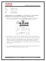
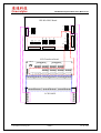
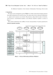
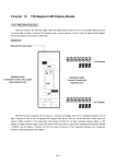
GPLB5X Development Board User Manual v0.1 January 28, 2008 GENERALPLUS TECHNOLOGY INC. reserves the right to change this documentation without prior notice. Information provided by GENERALPLUS TECHNOLOGY INC. is believed to be accurate and reliable. However, GENERALPLUS TECHNOLOGY INC. makes no warranty for any errors which may appear in this document. Contact GENERALPLUS TECHNOLOGY INC. to obtain the latest version of device specifications before placing your order. No responsibility is assumed by GENERALPLUS TECHNOLOGY INC. for any infringement of patent or other rights of third parties which may result from its use. In addition, GENERALPLUS products are not authorized for use as critical components in life support devices/ systems or aviation devices/systems, where a malfunction or failure of the product may reasonably be expected to result in significant injury to the user, without the express written approval of Generalplus. GPLB5X Development Board User Manual v0.1 0 TABLE OF CONTENT 0 Table of Content ................................................................................................................................................. 2 1 Revision History ................................................................................................................................................. 3 2 Introduction ........................................................................................................................................................ 4 2.1 Hardware Architecture........................................................................................................................ 4 2.2 GPLB5X Development component list ............................................................................................... 4 3 EMU Board......................................................................................................................................................... 5 3.1 GPLB5X EMU Board v1.1 .................................................................................................................. 5 4 Appendix A: GPLB5X EMU Board schematics..................................................................................................11 Generalplus Technology Inc. PAGE 2 Jan. 28, 2008 GPLB5X Development Board User Manual v0.1 1 REVISION HISTORY Revision V0.1 Date Jan,28, 2008 Generalplus Technology Inc. By Scott Remark Original PAGE 3 Jan. 28, 2008 GPLB5X Development Board User Manual v0.1 2 INTRODUCTION 2.1 Hardware Architecture The GPLB5X EMU Board is a shared board for GPLB52001A and GPLB52640A. emulate these devices on board. Programmer can easily Simply apply the following connection to start developing your project. Make sure power is properly supplied to both ICE and EMU board. GPLB5X EMU Board PC parallel port GENERALPLUS ICE A hardware overview of GPLB3X development system 2.2 GPLB5X Development component list Hardware 1. GPLB5X EMU board 2. Parallel connector (connects ICE & GPLB5X EMU board) 3. GENERALPLUS ICE (In-Circuit Emulator; sold separately) 4. Parallel port (connects to your personal computer; not included in the development kit) 5. Power supplier or adapter with 5V output (not included in the development kit). Software 1. FortisIDE software tool. (Please use version 3.0) Generalplus Technology Inc. PAGE 4 Jan. 28, 2008 GPLB5X Development Board User Manual v0.1 3 EMU BOARD 3.1 GPLB5X EMU Board v1.1 EMU chip: GPLB52001 Settings Description S1: VREG_OFF switch Name ON Enable Power VREG_OFF Regulator OFF Enable Power Regulator Function LCD Charge Pump control S2: Fixed and Don’t change. Generalplus Technology Inc. PAGE 5 Jan. 28, 2008 GPLB5X Development Board User Manual v0.1 S3: 32768Hz selector Name VCC 32768Hz Select R32K GND Function X32K 32768Hz source select S4: System clock selector Name VCC GND Sys_CLK X12M (12MHz X'TAL) X16M (ROSC) Function System Clock Select S5: Memory Selector (SRAM/ROM/FLASH) LED3: SRAM LED LED4: ROM LED LED5: FLASH LED S6: SW Number 1 2 3 4 5 6 7 8 Name -VREGS LCDS MONOS ROM_BOOT ---- SHORT OPEN 3.3V 16 x 74 MONO INTERNAL 2.6V 32 x 64 GRAY EXTERNAL Description N/A Power Regulator Selecter LCD dot size selecter LCD display mode selecter ROM Boot N/A N/A N/A S7: OPEN S8: Fixed and Don’t change. SW1: JP1~JP19: RESET Switch Common and segment socket J7, J9 and R4~R19 and J8, J10: Generalplus Technology Inc. Segment key scan output PAGE 6 Jan. 28, 2008 GPLB5X Development Board User Manual v0.1 J1, J2: PortA J2, J4: PortB J5, J6: PortC J11: ECLK, EXTI, IR Output connecter J12: SPI interface JK1: Adapter input (9V) JK2: General power input (5V) J20: General power input (5V) JK3: 3V VDD power Input J21: GND connecter LED1 : Power LED (ON when powered on) LED2: Sleep LED (ON while sleeping) LED3 : RAM LED (ON when switch S5 to RAM) LED4 : ROM LED (ON when switch S5 to ROM) LED5: FLASH LED (ON when switch S5 to FLASH) LED5 : DAC MONO LED(ON when Audio outputs are Dac mono ) LED6 : DAC STEREO LED(ON when Audio outputs are Dac stereo ) LED7 : PWM LED (ON when Audio outputs are PWM outputs) R22: System clock resistor (ROSC) R21: R32K resistor Y2: 12MHz X’TAL for System Clock Y1: 32768Hz X’TAL U1, U2: GPLB52001 Chip U3: CPU socket for ICE used U4,U5: RAM / ROM / FLASH, dependent on S5 U8: GPY0030 OP-AMP Generalplus Technology Inc. PAGE 7 Jan. 28, 2008 GPLB5X Development Board User Manual v0.1 SP1: PWM outputs speaker J14, J15: PWM output connector SP2: DAC output Speaker J13: DAC output connecter st Problems found in the 1 version GPLB52001: nd (estimated schedule of 2 st nd Mar/2008 ready, All 1 version boards need to be replaced by 2 1. version GPL52001 is version boards then) st VLCD is not stable in this GPLB52001 1 version, and GENERALPLUS can fix it in next version. If user wants to connect to LCD panel, It needs addition 8V power supply on VOUT pin of GPLB52001. 2. When GPLB52001 is selected to the mode of 4 Gray level ,32 COM x 64 SEG, the SEG60~SEG63 can not display correctly, SEG48~SEG51 data will be displayed on both SEG48~SEG51 and SEG60~SEG63. When GPLB52001 is selected to the mode of 4 Gray level, 16 COM x 74 SEG, the SEG70~73 can not display correctly, SEG58-SEG61 data will be displayed on both SEG58-SEG61 and SEG70~SEG73. But when GPLB52001 is selected to Black and White mode, no matter 32 COM x 64 SEG or 16 COM x 74 SEG mode, it is OK, no problem. 3. st This 1 version GPLB52001 EV board need to connect to a transform board to fix the wrong SEG sequence nd problem. Please see following diagram. It will be fixed in the 2 Generalplus Technology Inc. PAGE 8 version. Jan. 28, 2008 GPLB5X Development Board User Manual v0.1 GPLB5x EMU Board C16 C0 C8 C7 C15 C24 C23 C31 S0 S7 S40 S47 S56 S63 S8 S64 S71 S72 S73 S15 S32 S39 S48 S55 S24 S16 S31 S23 LCD Transform Board LCD PANEL Generalplus Technology Inc. PAGE 9 Jan. 28, 2008 GPLB5X Development Board User Manual v0.1 4 APPENDIX A: GPLB5X EMU BOARD SCHEMATICS Generalplus Technology Inc. PAGE 11 Jan. 28, 2008 GPLB5X Development Board User Manual v0.1 Generalplus Technology Inc. PAGE 12 Jan. 28, 2008