1
Constructing an Optical Phase-Locked Loop
for Partial-Transfer Imaging
of Bose-Einstein Condensates
André Lucas Antunes de Sá
Advisor: Professor David S. Hall
May 6, 2014
Submitted to the
Department of Physics of Amherst College
in partial fulfilment of the
requirements for the degree of
Bachelors of Arts with honors
c 2014 André Lucas Antunes de Sá
Abstract
Researching the dynamics of topological features within Bose-Einstein Condensates (BECs) can provide insight into the theory of superfluids and beyond.
Since these topological defects are often too small to be resolved in situ, the
BEC containing them must be released from its trap in order to be imaged. As
the location of these features cannot be easily controlled in the laboratory, the
study of their dynamics requires alternative approaches, such as imaging only
a fraction of the BEC at a time, a technique called partial-transfer imaging.
One of the ways in which a fraction of a BEC can be excited out of an optical trap is through stimulated Bragg-Raman transitions, which impart kinetic
energy to the atoms and change their internal state.
A procedure has been established for driving Bragg-Raman transitions on
87
Rb BECs in our lab, but it requires that two laser beams be phase-locked at
difference of approximately 6.835 GHz. For this purpose, we have designed and
constructed an optical phase-locked loop capable of maintaining a frequency
offset of 6.912 GHz between two independent diode lasers. We discuss methods
for tuning the loop, and we analyze the performance of the loop for several
iterations of the system. The final system performance still needs improvement
but is characterized by a square-mean phase error of x∆φ2 y = 0.39, equivalent
to 67.7% of the beat signal power in the carrier frequency. The loop should
be optimized before using it for experiments with BECs, and we suggest some
initial steps for addressing potential problems with the system. Finally, we
give an overview of the future laser system to be used in BEC experiments.
2
Acknowledgments
First, I would like to thank my thesis advisor Professor David Hall. Throughout my career at Amherst College, Professor Hall’s passion for teaching and
research has been a major inspiration to me. He taught me almost everything
I know about experimental science, and I am especially thankful for all the
numerous and memorable moments when he stopped to explain something to
me, whether it was the most simple concept to the most complex. Furthermore, my writing skills have improved greatly due to the breadth of feedback
he gave me from class reports and thesis drafts. This thesis project has given
me the opportunity to learn a great deal of things I expect to use in my future
career, and I am very happy that you were the one helping me along the way.
It has been a pleasure working with you and I look forward to hearing about
the exciting discoveries you will continue to make in the future.
I would also like to thank Michael Ray for all the help he provided during
my time in the lab, from aligning lasers, teaching me how to operate apparatuses, answering questions, and even driving me to class at a different campus
so I could stay longer in the lab. You have been of great help and also a
very enjoyable company. Nathan Thomas, whose project I attempted to move
i
forward with this thesis, was very helpful due to his well-written thesis and
well-documented procedures. I also want to thank Nigel Mevana for working side by side with me during the summer of 2013 and working on crucial
components for my experiment.
Jim Kubasek and Norm Page also deserve a special thanks. Jim taught
me everything I know about machining, and he machined himself many components needed for this thesis. Norm was always helpful with procuring components needed for my circuits and answering questions about component
choices.
The Physics Department at Amherst College deserves a major acknowledgement. I am very happy I got to interact with all of you through classes,
conversations, TA positions, leadership advising, grad school advising and so
many other important things in my life. I especially thank you all for teaching
me physics so passionately and I hope you keep spreading knowledge of this
beautiful science in such an enjoyable and enthusiastic manner.
I would also like to thank my fellow physics majors for all these years
together going through the toughest times. I am very proud to be a physics
major among you all and wish you the very best in your future life. I also
thank my friends both at Amherst and back at home who kept supporting
me through these years, especially my Karate teammates, Newman Club and
Electronics Club friends.
Finally I would like to thank my family and especially my parents. They
never gave up on my education and are phenomenal at helping me accomplish
my dreams. This thesis is dedicated to you Mom and Dad.
ii
The National Science Foundation has supported this research through grant
PHY-1205822, for which I am also very thankful.
iii
Contents
1 Introduction
1.1 Partial-Transfer Imaging of BEC . . . . .
1.2 Bragg-Raman Scattering . . . . . . . . . .
1.3 Optical Phase-Locked Loop Laser System .
1.4 Prospectus . . . . . . . . . . . . . . . . . .
.
.
.
.
.
.
.
.
.
.
.
.
.
.
.
.
.
.
.
.
2 OPLL Fundamental Theory
2.1 PLL . . . . . . . . . . . . . . . . . . . . . . . . . .
2.1.1 PLL Linear Analysis . . . . . . . . . . . . .
2.1.2 Loop Filter . . . . . . . . . . . . . . . . . .
2.2 PLL Synthesizer . . . . . . . . . . . . . . . . . . . .
2.2.1 Performance of Synthesizer and Phase Noise
2.3 Optical PLL . . . . . . . . . . . . . . . . . . . . . .
2.3.1 Laser as VCO . . . . . . . . . . . . . . . . .
3 OPLL System Construction
3.1 Lasers . . . . . . . . . . . .
3.2 ADF . . . . . . . . . . . . .
3.3 Loop Filter Implementation
3.3.1 Piezo Path . . . . . .
3.3.2 Current Path . . . .
.
.
.
.
.
.
.
.
.
.
.
.
.
.
.
.
.
.
.
.
.
.
.
.
.
.
.
.
.
.
.
.
.
.
.
.
.
.
.
.
.
.
.
.
.
.
.
.
.
.
.
.
.
.
.
.
.
.
.
.
.
.
.
.
.
.
.
.
.
.
.
.
.
.
.
.
.
.
.
.
.
.
.
.
.
.
.
.
.
.
.
.
.
.
.
.
.
.
.
.
.
.
.
.
.
.
.
.
.
.
.
.
.
.
.
.
.
.
.
.
.
.
.
.
.
.
.
.
.
.
.
.
.
.
.
.
.
.
.
.
.
.
.
.
.
.
.
.
.
1
2
3
5
6
.
.
.
.
.
.
.
7
7
9
17
21
23
25
26
.
.
.
.
.
27
29
33
35
39
41
4 OPLL System Performance
46
5 Bragg-Raman Ultimate Laser System
5.1 Optical Modules . . . . . . . . . . . . . . . . . . . . . . . . . .
58
60
6 Conclusion
65
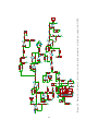
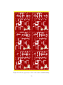
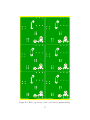
A OPLL System Schematics
67
iv
B Current Modulation
70
C Digital Control
76
v
List of Figures
1.1
1.2
Stimulated emission with counter-propagating laser beams. . .
Desired Imaging Transition. . . . . . . . . . . . . . . . . . . .
2.1
2.2
2.3
2.4
2.5
2.6
2.7
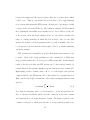
Block diagram of a PLL . . . . . . . . . . . . . . . . . . . . .
Block diagram of a standard negative feedback control loop. .
Phase margin and gain crossover for an example system. . . .
Block diagram of PI loop filter. . . . . . . . . . . . . . . . . .
Bode plots H(s) and E(s) for PI loop filter PLL. . . . . . . . .
Block diagram of PLL synthesizer. . . . . . . . . . . . . . . .
Block diagram of PLL synthesizer with dual-modulus prescaler.
Refer to text for in-depth explanation of the prescaler behavior.
Diagram of an OPLL implementation based on a PLL synthesizer.
2.8
3.1
3.2
Schematic of the OPLL system. . . . . . . . . . . . . . . . . .
2N5468 FET’s response (bottom) to a modulating Vgs signal
(top) at 1 MHz. . . . . . . . . . . . . . . . . . . . . . . . . . .
3.3 Photo of Evaluation Board . . . . . . . . . . . . . . . . . . . .
3.4 Third-order loop filter used in the OPLL. . . . . . . . . . . . .
3.5 Bode plots of charge-pump filters. . . . . . . . . . . . . . . . .
3.6 Loop filter’s amplifier stage . . . . . . . . . . . . . . . . . . .
3.7 Piezo feedback path. . . . . . . . . . . . . . . . . . . . . . . .
3.8 Bode plot of the transfer function of the integrator in the piezo
feedback path. . . . . . . . . . . . . . . . . . . . . . . . . . . .
3.9 Current feedback path. . . . . . . . . . . . . . . . . . . . . . .
3.10 Bode plot of the phase-advance filter. . . . . . . . . . . . . . .
3.11 Bode plot of both phase-advance loop filters. . . . . . . . . . .
3.12 Bode plot of current feedback path. . . . . . . . . . . . . . . .
4.1
4.2
4.3
Plot of power spectra of different board revisions. . . . . . . .
Phase noise spectra of the OPLL. . . . . . . . . . . . . . . . .
Phase noise spectra of the reference. . . . . . . . . . . . . . . .
vi
4
5
8
14
16
18
20
21
23
25
28
32
34
36
37
38
40
41
42
43
44
45
50
53
54
4.4
4.5
Bode plot of a lead-lag filter. . . . . . . . . . . . . . . . . . . .
Bode plot of current feedback path with lead-lag filter. . . . .
55
56
5.1
5.2
5.3
5.4
5.5
Diagram of the Bragg-Raman laser system . .
Diagram of the OPLL box. . . . . . . . . . . .
Diagram of the master/slave module. . . . . .
Picture of the Bragg-Raman module - OPLL.
Picture of the Bragg-Raman module - AOMs .
.
.
.
.
.
59
60
62
63
64
A.1 Simplified schematic of the Analog Devices evaluation board .
A.2 Schematic of the phaselock electronics board. . . . . . . . . . .
68
69
B.1
B.2
B.3
B.4
B.5
.
.
.
.
.
70
72
73
74
75
C.1 Digital control board schematic. . . . . . . . . . . . . . . . . .
C.2 Picture of the digital control prototype. . . . . . . . . . . . . .
77
78
.
.
.
.
.
.
.
.
.
.
.
.
.
.
.
.
.
.
.
.
.
.
.
.
.
.
.
.
.
.
Schematic of the current modulation board. . . . . . . .
Front copper layer of the board sent for manufacturing. .
Back copper layer of the board sent for manufacturing. .
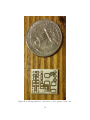
An unpopulated board next to a U.S. quarter dollar coin.
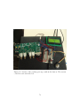
Picture of the board inside ECDL. . . . . . . . . . . . .
vii
.
.
.
.
.
.
.
.
.
.
.
.
.
.
.
.
.
.
.
.
Chapter 1
Introduction
Since the first dilute-gas Bose-Einstein Condensates (BECs) were produced
independently by groups at JILA and MIT [1, 2] in 1995, they have been
extensively used as a platform to study quantum mechanical systems at the
macroscopic level. In particular, because of the superfluid properties of BECs,
topological phenomena, such as quantized vortices, and its counterparts in
cosmology and condensed matter physics, such as coreless vortices [3, 4],
skyrmions [5, 6], and Dirac monopoles [7] can be observed. Study of these
features allows us to challenge and improve our understanding of superfluids
and beyond.
Since these topological features are small, in order to resolve them we must
release the condensate from its trap to allow it to expand. As the location of
tiny topological features within a BEC depends on the initial conditions of
their creation, attempting to reproduce a BEC experiment with the intention
of studying their dynamics is difficult. Hence, to study dynamics of these
1
microscopic features in BECs, we must be able to probe the same condensate
more than once in the same experiment.
A partial-transfer imaging technique has been used in our lab as a method
for studying the dynamics of vortices in BECs [8]. This method relies on
changing the spin angular momentum state of a BEC in a magnetic trap, from
a trapped to an untrapped state. Another limitation is that it restricts the
number of magnetic field configurations that can be applied to the condensate
while the trap is active, rendering creation of some topological defects such as
skyrmions and monopoles impossible.
To overcome some of these issues, we seek to use partial-transfer imaging with an harmonic optical trap, instead of using the magnetic trap. By
driving transitions between momentum states in optically trapped BECs, we
can extract atomic samples for imaging while keeping the rest of the BEC in
the trap, as has been described by Thomas [9]. Such a method requires two
phase-locked laser beams at a frequency difference of 6.835 GHz to drive suitable transitions for atom extraction. This thesis describes the theory, design,
construction and performance of an optical phase-locked loop to be used for
the extraction transition.
1.1
Partial-Transfer Imaging of BEC
Almost all of the information we can extract from a BEC requires a photograph
of its atomic density distribution. An absorption imaging technique is often
employed, in which a near-resonant laser beam illuminates a BEC, casting a
2
shadow on a CCD camera behind it. In order for the topological features to
be resolved, the condensate must be released from the trap and allowed to
expand to the point at which the features are visible. This imaging method is
destructive and only allows for one picture of a particular BEC.
If we are to study the dynamics of topological features however, some kind
of “non-destructive” imaging method must be employed. Freilich et al. [8],
developed a method for driving transitions between trapped and untrapped
spin states of a fraction of the atoms in a BEC by using microwave pulses. We
would like to use an analogous method for extracting atoms from an optical
trap, by change of momentum state of the atoms. Such transitions are called
Bragg transitions.
For more information on the BEC apparatus in our lab, see references
[10–14].
1.2
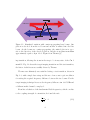
Bragg-Raman Scattering
As discussed by Thomas [9], by configuring two counter-propagating laser
beams of different frequencies to shine onto a
mentum changes of ∆p
87
Rb atom, we can impart mo-
2h{λ while simultaneously changing the internal
state of the atom, as shown in Fig. 1.1. We will refer to this type of transition
as a Bragg-Raman transition.
Since we need to extract only a small fraction of the trapped atoms for
imaging, while at the same time not disturbing the atoms in the optical trap,
Thomas decided that a transition to the |2, 0y state should be the target imag-
3
e
N Photons
N-1 Photons
N+1 Photons
N Photons
1
2
Figure 1.1: Stimulated emission with counter-propagating laser beams. One
photon is absorbed from the red beam and another is emitted into the blue
beam. As the beams are counter-propagating, the emitted photon is opposite to the direction of the absorbed photon, and the atom gains momentum
approximately equal to ∆p 2h{λ. Figure from Thomas [9].
ing transition, allowing the atoms in the trap to be in any state of the F
1
manifold. Fig. 1.2 shows the target imaging transition and the test transition,
the latter of which was successfully driven by Thomas.
Thomas was ultimately successful in driving a test transition, shown in
Fig. 1.2, with a single laser setup and the use of an acousto-optic modulator
for setting the required frequency difference between the two beams. For the
target imaging technique however, the frequency difference is 6.835 GHz and
a different method must be employed.
From his calculation of the fundamental Rabi frequencies, which correlate
to the coupling strength of a transition, he found the ratio
Ω|2,0y
Ω|1,1y
4
4.
(1.1)
52P1/2
2’,-2’
1’, 0’
Desired
Transition
2,-2
2’, 2’
∆2’,0’
1’,-1’
D1 Line
2’, 1’
2’, 0’
2’,-1’
∆1’,0’
1’, 1’
Test
Transition
2,0
2,-1
2,1
2,2
~6.835GHz
52S1/2
1,-1
1,0
1,1
Figure 1.2: Desired Imaging Transition and Thomas’ test transition are shown.
Both transitions require that the beams are detuned from the |11 , 01 y. For the
desired transition, the beams must be 6.835 GHz apart. Figure from [9].
for the Rabi frequencies of the test transition and of the target imaging transition. Thus he concluded that the target imaging method was likely to work
with minimal modification of the apparatus he used.
1.3
Optical Phase-Locked Loop Laser System
In order to achieve the frequency difference of 6.835 GHz between the two
beams for driving the desired imaging transition, we decided to phase lock two
independent lasers. This system uses the beat signal between the two lasers
as an input to a phase-locked loop synthesizer. Phase-locking is achieved by
allowing the loop to control one of two lasers. This method has the advantage
5
of being low-cost and flexible. Another method would be to employ a high
frequency acousto-optic modulator to increase the frequency of a laser to 6.835
GHz, which would be conceptually similar to the scheme Thomas used [9].
Acousto-optic modulators with such a large bandwidth tend to be expensive
[15] and the advantage they offer in simplicity of integration does not outweigh
its cost, in our judgement.
1.4
Prospectus
In the remainder of this document, we study the design, construction and
performance of an optical phase-locked loop system for driving Raman transitions in a BEC. In Chapter 2 we will study the fundamental theory behind
a phase-locked loop, how phase-locked loop synthesizers work, how to optimize a synthesizer, and, finally, how to construct an optical phase-locked loop.
In Chapter 3, we reveal our implementation for an optical phase-locked loop
with the goal of eventually driving the imaging transition in
87
Rb atoms. In
Chapter 4 we characterize the system performance and discuss improvements.
For Chapter 5 we describe the overall laser system that will be used in our
laboratory for experiments with BECs using the Raman transitions.
6
Chapter 2
OPLL Fundamental Theory
Optical phase-locked loops (OPLLs) have been constructed for the past few
decades to study a variety of physical phenomena that requires coherence of
laser beams, such as electromagnetically induced transparency (EIT) [16, 17],
cold atom interferometry [18], frequency metrology [19] and many others.
Since OPLL construction is mainly motivated by research in optics laboratories, most OPLL systems are implementation-specific and there is no general
primer on their design. The common ground for understanding OPLL systems, the heart of the system, is usually an electronic phase-locked loop. The
fundamental theory behind phase-locked loops extends naturally to OPLLs
and for this reason, we first delve into analysis of standard phase-locked loops.
2.1
PLL
A phase-locked loop (PLL) is a negative feedback control system that drives
the phase of an oscillator to track the phase of a reference oscillator. We define
7
phase to be the argument of the analytic representation of a signal, i.e., for a
simple sinusoidal
φ A cospwt
θq,
(2.1)
where A is the signal’s amplitude, w is the angular frequency and θ is the phase
offset. An electronic PLL usually consists of the following essential elements: a
phase detector (PD), a loop filter (LF), a voltage-controlled oscillator (VCO),
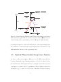
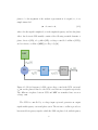
and a reference oscillator (REF) (see Fig. 2.1) [20].
REF
PD
LF
VCO
Figure 2.1: Block diagram of a PLL. vc ptq voltage controls the VCO. φo ptq and
φref ptq are the phases related to the VCO’s and reference’s signals respectively.
The difference in phase between VCO and REF are translated into an error
voltage vd ptq.
The VCO is controlled by a voltage input vc ptq and generates an output
signal with frequency ωo ptq and phase φo ptq. The reference oscillator provides a
known stable frequency signal to which the PLL can phase lock, with frequency
8
ωref ptq and phase φref ptq. VCO and REF signals are compared at the PD, which
outputs an error voltage, vd ptq, based on the phase difference between the two
inputs given by
φe ptq φref ptq φo ptq.
(2.2)
The error voltage is then processed by the loop filter to become the control
voltage of the VCO, thus closing the feedback loop.
The negative feedback causes the control voltage to modulate the VCO
center frequency, adjusting φe to a constant. Since frequency is the time
derivative of phase, phase tracking also means that ωo ptq
ωref ptq.
The loop
is considered locked when the average frequency of the VCO, set by the vc
offset, is equal to the average frequency of the reference oscillator. If we place
frequency dividers in the feedback path and between the PD and the REF,
we can make ωo ptq proportional to ωref ptq by a constant. Hence, the system
will become a frequency synthesizer using the REF as a timebase. We discuss
PLL synthesizers in Sec. 2.2.
In the next subsections we develop a linear model for PLLs and use it
to study specific system configurations. We also develop the language for
characterizing the performance of PLLs.
2.1.1
PLL Linear Analysis
Although PLL systems are inherently nonlinear, a linear model is applicable
when phase error is small, which is a condition normally attained when the loop
is locked [20]. Note that phase error in this case includes the phase difference
9
between the inputs and the expected phase offset the loop introduces, which
could be zero. Thus we can analyze the steady-state loop by approximating
it as a linear time-invariant (LTI) system, allowing us to use many powerful
concepts and tools from LTI theory. The nonlinear analysis of PLLs is much
more challenging but luckily is not usually needed. As we will see at the end
of the section, from the linear analysis alone we can reliably calculate the
range of certain parameters at which the lock is stable. Also, for any PLL
system, the negative feedback guarantees the loop will eventually come close
to a frequency lock and enter the linear regime of the loop, further justifying
our linear analysis.
LTI systems have remarkable properties that make them relatively easy
to study. Most of the design guidelines for the construction of PLLs stem
from powerful analytical tools developed for LTI systems [20]. A fundamental
result of the theory is that any LTI system can be characterized entirely by
a single function, the system’s impulse response hptq in the time domain [21].
Equivalently, in the s-domain, where s
σ
iω is the Laplace independent
complex variable, any LTI system can be characterized by a transfer function
H psq, which is the Laplace transform of the analogous impulse function hptq
given by
L thptqu »8
0
est hptqdt.
(2.3)
Note that the imaginary part of s, the frequency ω, is the independent variable of a Fourier transform, which can take a function in the time domain
and transform it to one in the frequency domain. The Laplace variable s also
contains a real part, σ, which gives the rate of an exponential growth/decay,
10
necessary for characterizing systems governed by differential equations with
exponential solutions. The s-domain and the frequency domain are used interchangeably in control theory. Hereafter we shall refer to the s-domain as
the frequency domain. Also, we use lowercase letters, aptq, to describe impulse
response functions and uppercase letters, Apsq to describe transfer functions.
Note that for any impulse function aptq
aptq L 1 tApsqu ,
(2.4)
and for any transfer function Apsq
Apsq L taptqu .
(2.5)
In the time domain, the output of an LTI system will be equal to the
convolution of the input function and the impulse response, i.e. voutput ptq
vinput ptq hptq. In the frequency domain, the output is simply Voutput psq Vinput psq H psq, since the Laplace transform of a convolution of two functions
is equal to the multiplication of the Laplace transforms of the functions. This
is a powerful property, as it allows us to model any LTI system and find
its transfer function by knowing the transfer functions of smaller individual
subsystems.
We shall now analyze a PLL by taking advantage of the properties discussed
above. As we stated before, the primary purpose of the loop is to phase lock
the two oscillators as opposed to simply frequency locking them. Frequency
lock follows naturally from the phase lock. Thus, we want to focus on how the
11
system transforms the input phase signals. The following derivation has been
adapted from Gardner [20].
Consider a PLL of the sort depicted in Fig. 2.1 and assume the loop is
locked. For a linear PD with gain Kd and dimensions of voltage, we expect
the error voltage output of the PD to be
vd ptq Kd φe ptq.
(2.6)
The error voltage vd is then processed by the loop filter. The loop filter
is essential in the design of a PLL as it allows tuning of the PLL’s performance parameters. We will expand the discussion on loop filters in Sec. 2.1.2
and 2.3.1, and describe the loop filter used in our OPLL system in Sec. 3.3.
For now, we will use a generic impulse function, f ptq, to characterize the loop
filter. The output of the filter, i.e., the control voltage, is
vc ptq vd ptq f ptq,
(2.7)
If we assume the VCO is also linear, with a gain Ko and dimensions of frequency/voltage, then its frequency will be given by ∆ω ptq
Kovcptq
w0 ,
where w0 is the VCO center frequency. Since frequency is the derivative of
phase φo , the VCO operation may be described as
dφo
dt
Kovcptq,
(2.8)
where we omit the center frequency w0 as we are only concerned with the
12
loop’s relative phase tracking behavior. Taking the Laplace transform of both
sides of Eq. 2.8, L tdφo {dtu sΦo and L tKo vc ptqu Ko Vc psq , we arrive at
the phase relation of the VCO output in the frequency domain
Φo psq Ko V c p sq
,
s
(2.9)
from which we confirm that the phase of the VCO is proportional to the integral of the control voltage, since 1{s is the Laplace transform of an integration,
as expected from Eq. 2.8.
We can now write the system’s response to a phase error signal at the input
by using the relations in Eqs. 2.6 and 2.7 for the control voltage Vc psq:
Φo psq Ko Vc psq
s
KdVopssqF psq Φepsq KdsKo F psq.
(2.10)
Since a PLL is a negative feedback loop, we can condense the individual
subsystems from Fig. 2.1 to that of a general negative feedback loop [22], as
seen in Fig. 2.2. This warrants a description of the system by means of overall
transfer functions standard to control loops, which will be very useful for all
the subsequent analyses.
From Eq. 2.10, we find the open-loop transfer function of the system Gpsq,
which describes how the system processes a phase error Φe psq input, to be
Gpsq Φo psq
Φe psq
KdKsoF psq .
(2.11)
Note that a PLL will not function properly in the open-loop condition, but the
13
In(s)
E(s)
Out(s)
G(s)
H(s)
Figure 2.2: Block diagram of a standard negative feedback control loop. H psq
is the transfer function of the overall system, including feedback.
open-loop transfer function, also called open-loop gain, is a valuable concept
in the analysis of the system.
With the feedback implementation, we arrive at two new transfer functions,
the system transfer function H psq and the error transfer function E psq. These
functions describe how the phase of the reference signal Φref appears at the
output of the PLL and at the phase error Φe psq respectively. The system
transfer function, sometimes also called the closed-loop gain, is given by
H p sq Φo psq
Φref psq
1 GpGsqpsq s KdKKoKF pFspqsq ,
d
14
o
(2.12)
and the error transfer function is given by
E p sq Φe p sq
Φref psq
1
1
Gpsq
1 H psq s
s
.
Kd Ko F psq
(2.13)
We observe that the behavior of the system transfer function is akin to that of
a low-pass filter, since the gain decreases as frequency increases. The opposite
is true for the error transfer function, which acts as a high-pass filter. Since the
steady-state error will be given by the limit of E psq as s Ñ 0, we can already
infer that a larger gain Kd Ko F psq, later defined as the loop bandwidth, will
lead to a smaller phase error.
Furthermore, the open-loop transfer function can be written as the ratio
of two polynomials A and B, which are useful for describing the system. The
system transfer function then becomes
H p sq Apsq
.
B psq Apsq
(2.14)
This simplification will aid in the understanding of the shape of the transfer
functions and the stability of the loop.
For any negative feedback loop, when
|Gpsq| 1
ArgrGpsqs 180 deg
(2.15a)
(2.15b)
the denominator of Eq. 2.12 is undefined, and it becomes clear the loop will be
completely unstable. This is due to the feedback flipping sign and resulting in
15
infinite gain on the phase error signal. At this point, it is useful to introduce the
concept of a phase margin, equal to the absolute value of the phase introduced
by the system minus 180 at the frequency where the gain is 1, also called
the gain crossover frequency [23]. The loop is guaranteed to be unstable if the
phase margin is negative. Fig. 2.3 shows two plots of the frequency response to
the magnitude and to the phase of the input signal, collectively called a Bode
plot, of a system transfer function with one zero at 1, and a second-order pole
at the origin. The crossover frequency happens at ωc
is
70.5.
?
2, where the phase
Thus, the phase margin is 109.5 and the system is far from being
unstable at all frequencies. Also a similar concept to the phase margin is the
gain margin, which is 1 minus the gain at which the phase introduced by the
system is 180 .
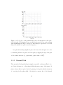
Figure 2.3: Bode plot of H psq
and phase margin 109.5 .
s 1
s 1
s2
p
q p q , with gain crossover at ωc
?
2
A PLL can also be categorized by its order and its type. The order of the
PLL is given by the degree of the characteristic polynomial. The type of a
PLL refers to the number of integrators in the loop. Each integrator in the
16
system contributes one pole to the transfer function, so that the order can
never be less than the type. Non-integrating components in the loop filter
can also contribute poles to the transfer function but the type will not be
affected. Type 2 PLLs are extremely common for PLL synthesizers owing to
the widespread use of digital phase-frequency detectors, as we will discuss in
Sec. 2.2. We will focus only on type 2 PLLs in our discussions henceforth.
With certain care, we may ignore the effects of an extra integrator in the loop
filter and still arrive at a reasonable description for a type 3 PLL [20].
2.1.2
Loop Filter
In the previous section, we did a preliminary study of the transfer functions
governing a PLL, but we cannot say much more before specifying a loop filter
transfer function F psq. The loop filter is generally the most flexible part of
the PLL system, allowing the engineer to tune the PLL design with the goal
of satisfying the needs of a certain application.
Anticipating the use of a proportional-plus-integral (PI) filter in the OPLL
system, we shall choose its transfer function now to complete our characterization of PLLs. This is the simplest filter that can be used with the type of
phase detector chosen for the OPLL system, which outputs a current signal
with the phase error information. Later in Sec. 3.3 we discuss the use of a
higher-order filter. The transfer function for a PI filter, as seen in Fig. 2.4, is
given by
F psq K1
17
K2
,
s
(2.16)
where K1 is the dimensionless coefficient of the proportional path through the
filter and K2 , with dimensions of frequency, is the coefficient of the integral
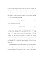
path.
𝑉d (𝑠)
+
𝑉c (𝑠)
𝐾2
𝑠
Figure 2.4: Block diagram of PI loop filter implemented as the loop filter in
Fig. 2.1. The proportional path is the top one while the integral path is the
bottom one. Their sum results in Vc .
The system transfer function, Eq. 2.12, then becomes
H psq Kd Ko pK1 s K2 q
.
sKd Ko K1 Kd Ko K2
s2
(2.17)
As it is, the system is overdetermined and can be parametrized. Since we
have a second-order loop, all we need are two parameters to describe the whole
system. A very useful parameter, that will be used extensively later on, is the
loop gain K, which is defined as
K
Kd K o K1
18
(2.18)
for a second-order type 2 PLL. Note that the integral gain K2 did not enter
into the definition of K. In fact, more generally, the loop gain for any PLL
is determined entirely by the proportional path of the filter while integrators
and other frequency-dependent responses are not involved in its definition at
all [20]. Nonetheless, the loop gain has a dominant influence on the loop
bandwidth as we will see below.
Using K to parameterize the system and the error transfer functions,
Eqs. 2.12 and 2.13 respectively, we arrive at
H p sq K ps 1{τ q
,
s2 Ks K {τ
(2.19)
E psq s2
,
Ks K {τ
(2.20)
s2
where τ is the second parameter needed to describe the system. Bode plots
of these transfer functions are shown in Fig. 2.5. Note the low-pass filtering
effect of H psq and high-pass filtering effect of E psq. Also note how the loop
gain traces the corner frequency of the graph. As a matter of fact, for any
PLL the loop gain is a strong indicator of the low-pass corner frequency [20]
and for this reason we shall refer to it as the PLL loop bandwidth.
We could also adopt natural frequency and damping parameters for describing the PLL, which are analogous to a damped harmonic oscillator, also a
second-order system. We will not derive this approach here, but it is a common
means of analysis used by many textbooks in control theory [20, 23]. From
the Bode Plots in fig. 2.5, the peak we see for gain greater than 0, especially
pronounced when K
1, is strongly dependent on the damping parameter.
19
Figure 2.5: Bode plots of Eq. 2.19 and 2.20 with τ =1 and K 1, 10 and 100
from top to bottom. Note how K is a good indicator of the corner frequencies.
Furthermore, many authors use the natural frequency to refer to the loop
bandwidth of the PLL. Even though most common definitions of loop bandwidth are somewhat related to each other, care must be taken when comparing
them.
20
2.2
PLL Synthesizer
As we suggested in the beginning of Sec. 2.1, by placing frequency dividers in
the PLL, we can generate any desired frequency using the reference oscillator
as timebase. Consider a basic version of a PLL synthesizer in Fig. 2.6. Frequency dividers N and R reduce the frequency of the VCO and REF oscillators
respectively to a comparison frequency fc at which the signals are compared
by the PD. Note that f
ω{2π.
From the phase and frequency relationship
we discussed in Sec. 2.1, the VCO frequency will be given by
fo
fRref N N fc.
(2.21)
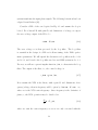
REF
𝑓ref
1/R
𝑓c
PD
LF
VCO
𝑓o
𝑓c
1/N
Figure 2.6: Block diagram of PLL synthesizer. Dividers R and N are placed
in order to have the VCO not only phase lock to the REF but also output a
signal at a frequency fo N fref {R.
21
Digital counters are extremely popular as frequency dividers given that
they are low-cost, can provide large division ratios and can be programmable.
They also have disadvantages when compared to analog dividers, mainly their
large bandwidth makes them noisier than an analog divider of the same division
ratio [20]. Use of a digital counter also constrains the choice of associated
phase detector. Typically a phase-frequency detector is used, which has the
advantage of ensuring the loop enters the linear regime quickly. As the system
can be entirely placed in a single IC, this configuration is prevalent in the
construction of PLL synthesizers.
For VCOs operating at GHz frequencies, it may not be feasible to find an
effective counter for N [22]. In such cases where a large division is needed between the VCO and the PD, a prescaler, essentially a second digital counter,
is used in the feedback path. There is more than one type of prescaler implementations, we focus on the dual-modulus prescaler since it is the prescaler
used in our chosen OPLL synthesizer.
A dual-modulus prescaler, illustrated in Fig. 2.7, offers the advantage of
having the frequency spacing resolution, i.e., the possible frequency output
for given programmable counters, of fc as is the case with a single N counter
but which would not be the case of two cascaded N counters. The prescaler
works as the following for each comparison cycle: At the start of the cycle
the prescaler divider is set to P+1, and A and B counters are set to their
programmed maximum value; each count from the prescaler decrements both
A and B until A reaches 0; at this point counter B still has pBinitial Ainitial q
counts left until it reaches 0, and the prescaler switches to a division of fo by
22
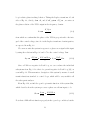
REF
𝑓ref
𝑓c
𝑓o
1/R
PD
LF
VCO
𝑓c
1/B
Reset
1/P
1/(P+1)
1/A
Select P
or P+1
Figure 2.7: Block diagram of PLL synthesizer with dual-modulus prescaler.
Refer to text for in-depth explanation of the prescaler behavior.
P; when B reaches 0 a count is outputted to PD and the cycle resets. This
behavior yields an equivalent comparison counter N where
N
2.2.1
pB AqP
ApP
1q BP
A.
(2.22)
Performance of Synthesizer and Phase Noise
The performance of a PLL synthesizer is commonly tested on grounds of stability and fast acquisition. Long term stability refers to the drift of the center
frequency over long periods of time. Short term stability of the synthesizer is
typically quantified by the residual phase noise of the VCO and is the most
important noise measure for our experiments.
23
For an ideal PLL, following any phase drift of the VCO or REF, resulting in
a non-zero φe , the loop instantaneously adjusts the VCO for perfect tracking of
the reference. In practice however, we observe the effects of phase noise, related
to the amount of error in the phase tracking of the loop at any time. Noise
generated anywhere in the PLL can contribute to phase noise as it propagates
to the VCO. Large phase noise greatly decreases the performance of a PLL
as the tracking errors can drive a PLL out of its linear regime. For small
phase noise, where the loop maintains lock, we can treat the noise linearly
such that the overall phase noise is a superposition of all the noise generated
in the system. The system error response, Eq. 2.13, provides insight into the
phase noise of the loop.
From Gardner [20] we find that for a PLL synthesizer the following is true
regarding phase noise:
• Additive noise occurring between the phase detector and the filter is
lowpass-filtered by the PLL;
• A large PD gain Kd is favorable for reducing the effects of additive noise
arising before the loop filter;
• Small VCO gain Ko is favorable for reducing the effects of additive noise
arising after the loop filter.
Also note that, from the introduction of the N and R counters, the error
transfer function gets multiplied by the ratio N {R as any noise from the reference gets divided by R, while noise at the PD gets multiplied by N . Therefore
the ratio N {R should be minimized in the PLL synthesizer design.
24
2.3
Optical PLL
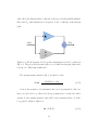
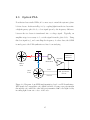
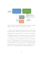
Now that we have studied PLLs, it becomes easy to extend the system to phase
lock two lasers. As shown in Fig. 2.8, by coupling light from the two lasers into
a high-frequency photodiode, a beat signal given by the frequency difference
between the two lasers is transformed into a voltage signal. Typically, an
amplifier stage is necessary to boost the signal from the photodiode. Using
this beat signal as fo and controlling the frequency of a slave laser, the OPLL
is analogous to the PLL synthesizer we have been studying.
BSC
Fast
Photodiode
Amplifier
Reference
Oscillator
Master
Laser
Piezo
Slave
Laser
PLL Synthesizer
Circuit
Current
Figure 2.8: Diagram of an OPLL implementation based on a PLL synthesizer.
BSC stands for beam splitter cube which lets half of beam power pass straight
through the cube while the other half gets transmitted 90 to the right for any
incoming light beam onto a face of the cube.
25
2.3.1
Laser as VCO
There are two main mechanisms through which a typical OPLL controls a slave
laser: (1) modulation of the laser’s injection current, and (2) modulation of the
cavity length through the use of a piezoelectric device. The current modulation
response has a large bandwidth and it is the most important for correcting
phase noise due to high-frequency disturbances. The piezo is constrained to
a bandwidth of a few kHz [24], and is responsibly for maintaining long-term
stability due to mechanical vibrations or temperature drifts.
It is important to note though that the frequency of semiconductor laser
diodes depends on the current through two effects that dominate at different
frequency ranges: carrier density effect at high modulation frequencies, which
affects the refractive index of the gain medium, and temperature of the recombination area [21]. These two effects actually oppose each other, being
equivalent to a phase shift of 180 in the laser’s frequency response at the
thermal cutoff frequency, at which the temperature effect ceases to dominate
the response and the carrier density effect takes over. It is clear from the
conditions in Eq. 2.15 that this phase shift can drive the loop unstable. We
discuss solutions to this problem in Sec 3.3.2.
26
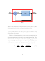
Chapter 3
OPLL System Construction
We build our OPLL system by carefully selecting components that not only
enable a phase lock but that also minimize the residual phase noise of the
system. As discussed in Sec. 1.2, Thomas [9] was able to drive a test transition,
and, given the result of his calculation in Eq. 1.1, we expect similar results
when driving the target imaging transition with the OPLL system. Our OPLL
is based on many other implementations of OPLLs from the past couple of
decades, especially on that of Appel et al. [24]. Our apparatus schematic is
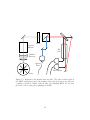
shown in Fig. 3.1 and we briefly explain it below.
The most important part of the OPLL is the phase detector. For their lowcost, high reliability and ease of integration into an OPLL system, we choose
Analog Devices’ ADF family of PLL synthesizers, which integrates a PFD and
digital counters in a single chip. In fact, we decide to use the evaluation board
made by Analog Devices as it is already a working and documented system
which we can easily modify for our purposes. We discuss our choice of ADF
27
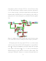
FP
Master
Laser
BSC
1481-S
Photodiode
Directional
Coupler
ZX-60-8008E
Amplifiers
ADF
Board
To Spectrum
Analyzer
Ref
Slave
Laser
Piezo
Feedback
Processing
Current
Figure 3.1: Schematic of the OPLL system. The blue rectangle indicates a
physical box constructed for this system, which powers the photodiode, the
amplifiers, the ADF eval. board and the feedback processing board. Compare
with standard OPLL diagram in Fig. 2.8. See Chapter 5 for more information
on the physical box.
chip, optimal settings, reference oscillator and all required modifications in
Sec. 3.2.
Since the desired frequency difference between the two lasers is
7 GHz,
the photodiode must have an equally large bandwidth. We choose the New
Focus 1481-S high-speed photodiode, which has a 3-dB bandwidth of 25 GHz.
With a responsivity of around 0.37 A/W, transimpedance gain of 25 V/A, and
saturation power of 2 mW, we expect the maximum power output to be 22
dBm. Since the ADF requires an input of at least 5 dBm, an amplifier stage
composed of three Minicircuits ZX-60-8008E microwave amplifiers is added
28
after the photodiode. The amplifier is then connected to a -20 dB directional
coupler, where the transmitted power, with loss of
0.04 dBm, is forwarded
to the ADF input, and the coupled signal is routed to a HP563A spectrum
analyzer for characterization of the system.
In order to facilitate the locking procedure, we also add a Fabry-Perot
interferometer (FP) to the system. This allows the user to set the frequency
of the slave laser near the desired frequency difference from the master laser,
and also allows the user to ensure that the slave laser’s frequency can be freely
tuned while the laser is in a stable regime.
In the next sections we will further describe some of these elements. The
last section, about processing of the piezo and current feedback loop, is of
great importance to the tuning of the OPLL, which we discuss in the next
chapter.
3.1
Lasers
The master and slave lasers are external cavity diode lasers (ECDLs) with
diodes, QLD-795-150 from Qphotonics, of 795 nm nominal wavelength, and
are both thermally stabilized. The master laser’s injection current is controlled
by an analog-based controller, while the slave laser is driven by a more robust
controller, which can be set by programming an internal digital-to-analog converter instead of a commonly used potentiometer. This digital programming
feature has not yet been implemented but is expected to be used in the final
system (See Chapter 5). During all performance measurements of the OPLL,
29
we used the slave laser’s current control with a potentiometer.
The master laser, which is the same laser used by Thomas in his singlelaser setup, is locked to an atomic transition in Rb using saturated absorption
spectroscopy. The actuators in the feedback control loop of this lock are the
same as in our OPLL system: current modulation and external cavity length
modulation. We use the lock mechanism to stabilize the laser frequency, reducing its contribution to phase noise. In the future we will use the lock to set
the detuning frequency for the Raman transition as discussed by Thomas [9].
Note that Thomas used a dichroic-atomic-vapor laser lock (DAVLL) for his
experiments driving Raman transitions, and he cites their advantage of providing lockable slopes up to 500 MHz from the desired excited state resonance.
Since we will be using acousto-optic modulators (AOM) for the Raman beams
that have a 3-dB bandwidth of
68 MHz [25], we anticipate that a DAVLL is
unnecessary.
The slave laser cavity was machined at Amherst College following the
blueprints from Cook et al. [26]. This ECDL is built out of a single piece
of aluminum and is optimized for thermal stability and vibration suppression.
Our cavity is slightly modified from that of Cook et al. in order for us to
use it in the OPLL system. These modifications include adjustment of the
grating arm for better compatibility with a 795 nm laser and adaptation of
the connector interface to include space for the current modulation connector
and wiring. Although the system was built to be airtight, we did not use a
vacuum on the cavity for our experiments. Nonetheless, we sealed the cavity,
shielding it from the lab environment.
30
As we have discussed in Sec. 2.3.1, there are two standard ways of controlling the frequency of an ECDL: modulating the injection current and varying
the cavity length through use of a piezoelectric transducer (piezo). For the
current modulation, we choose to build a small board with a field-effect transistor (FET), MMBF5484, able to sink or source current to the diode inside
the cavity. The board was manufactured to be placed right next to the laser
diode, allowing local modulation of the current from a voltage signal. For more
information on the construction of the board see appendix B. This FET-based
solution needs to have a bandwidth large enough to allow correction of the
fastest noise-induced instabilities of the ECDLs, which typically spans a few
MHz [24]. By using a current sensing op-amp circuit, we studied the board’s
response when modulating current though a 100 Ω load resistor at 5 V. We
found that for frequencies up to 5 MHz, the FET’s response was remarkably
linear with minor frequency dependent amplitude variations and phase lag.
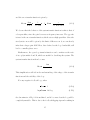
Fig. 3.2 shows the FET response to a 1 MHz modulating signal Vgs between
1.4 V and 1.4 V. These results were in agreement with earlier testing of
an analogous FET, 2N5468, modulating the current flowing through a simple
LED circuit. We could not reliably test higher modulation frequencies because
of our measuring circuit’s limitations, mainly stray capacitance and high inductance typical of a breadboard. Nevertheless, the MMBF5484 is expected
to function with minimal noise and insignificant transadmittance variations at
up to 200 MHz. At DC, modulation of
1mA is observed between Vgs equal
to 1.4 V and 1.4 V. Note that the FET board contains a phase-advance loop
filter, which will be important in Sec. 3.3.2 when attempting to correct for
31
phase shifts in the current modulation path.
Figure 3.2: 2N5468 FET’s response (bottom) to a modulating Vgs signal (top)
at 1 MHz.
A piezo stack is used to displace the feedback grating of the ECDL by a
few microns as described by Cook et al. [26]. It is imperative that no negative
voltages are applied to the stack as they could be damaged. The bandwidth of
a piezo is typically a few kHz, and it is not as important for minimizing phase
32
noise as the current modulation, since we expect it to only correct for slow
phase drifts between the lasers. It is still important for the OPLL system as
it can provide a bigger capture window for the lock, i.e., the range of fo where
the OPLL can reliably lock, thus assuring long-term stability and significantly
aiding the current modulation in reducing phase noise at the low-frequency
range. We could have put a high-pass filter on the current feedback so as to
rely only on the piezo for the low-frequency corrections, but we chose not to
do so for this prototype.
3.2
ADF
As discussed by Thomas [9], we require the two Raman beams to be at a
frequency of 6.835 GHz apart [27]. For its successful use in an OPLL [24], and
for its great versatility and simplicity, we choose the ADF4107 synthesizer
chip for the OPLL system. The ADF4107 contains a PFD, a 14-bit R counter,
a dual-modulus prescaler with allowed N values from 24 to around 105 , and
its maximum frequency output is 7 GHz. Another advantage of choosing
the ADF family of PLL synthesizers, is that Analog Devices distributes a PLL
simulator, ADIsimPLLTM , compatible with all ADF chips, which can aid us in
the preliminary design of the system and also allows saving ADF chip settings
to a file for easy reprogramming.
The evaluation board for the ADF4107, EV-ADF411XSD1Z, is shown in
Fig. 3.3. We choose to use this board in our system since it can easily be
modified to our needs thus avoiding design and testing of a new microwave
33
board, which would require knowledge of microwave circuit design and expensive board testing tools. The evaluation board comes with a slot where the
ADF USB programmer, SDP-S, can be attached.
ADF4107
Analog Devices SDP-S
Loop Filter
VCO
Figure 3.3: Photo of the Evalution Board from Thomas [9].
In order to use the evaluation board with an external reference oscillator
and VCO, we need to remove or replace components on the board. A simplified
schematic of the evaluation board with the alterations in place is shown in
Fig. A.1, in appendix A.
From our discussion in Sec. 2.2, to minimize phase noise we must make
sure the ratio N {R is as small as possible. Since the maximum allowed REF
34
frequency (fref ) is 250 MHz, the maximum PFD frequency (fc ) is 100 MHz,
and the output frequency must be close to 6.835 GHz, we decide that the
optimal set up for the ADF, also discussed by Appel et al. [24], is:
• fo = 6.912 GHz;
• fc = 72 MHz, with N = 96 (P = 32);
• fref = 216 MHz, with R = 3.
As the reference oscillator, we use the HP8647A signal generator with
frequency output of 216 MHz at 0 dBm. A 10-MHz timebase is provided
to the reference and to the spectrum analyzer from a rubidium clock.
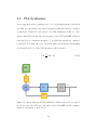
3.3
Loop Filter Implementation
In Sec. 2.1.2, we stated that the loop filter provides our system design with
some flexibility, with which we can compensate for issues arising in other elements of the OPLL. The first part of the loop filter is a charge pump filter for
the output of the ADF chip, which generates charge pulses proportional to the
phase-frequency deviation of the two input signals. This initial filter can be
placed right on the evaluation board, since the current signal is more susceptible to noise than the filter voltage output. Due to the pulsed-nature of the
charge-pump output, and in order to minimize reference spurs and jitter caused
by the modulation of voltage output, we use a third-order filter rather than a
second-order filter, which does not include C2*. We use ADIsimP LLTM to
find a versatile setup for this first stage filter, i.e. values for the components
35
in the filter that allow us to tune the system using the subsequent stages of
filtering, as it is impractical to tweak the value of surface-mount components.
For this reason we use 150 Ω for R1*, 5.6 nF for C1* and 33 nF for C2*. These
values were not changed throughout the characterization of the system.
Figure 3.4: Third-order loop filter consisting of a PI stage plus a capacitor
to ground. All of these components are soldered directly onto the evaluation
board. With the removal of C2* the filter becomes second-order.
A plot of the transfer functions of the second-order and the third-order
charge-pump loop filters can be seen in Fig. 3.5. Note that a big disadvantage
of using the capacitor C2* is that the overall negative phase shift decreases
the phase margin. Furthermore, increasing the overall loop gain increases the
phase shift, bringing down the phase margin even lower. We must be really
careful with this effect because it can easily cause the OPLL to be unstable if
36
any more negative phase shift is introduced. There is also a clear advantage
of using the third-order filter and placing the extra pole at higher frequencies
as the rate at which the amplitude response decays is smaller, allowing for
better high-frequency response of the current feedback path as we will see in
Sec. 3.3.2.
Figure 3.5: Bode plot of a second order charge-pump filter, as seen in Fig. 3.4
wihtout C2* (left), and of a third-order charge-pump filter with the addition
of C2* (right).
The next stages in the feedback need to transform the transfer function of
the system to increase performance, as well as to translate the voltage levels
for compatibility with the piezo stack and the current modulation board. The
first subsystem, seen in Fig. 3.6, is built into a new board, which we shall refer
to as the feedback board. A twisted pair of wires connects the output of the
37
charge-pump loop filter to the input “CP Vout” of the feedback processing
board. Since this next stage contains no frequency-dependent components, it
does not change the shape of the filter’s transfer function in the functional
frequency regime of the PLL, but it does add a gain factor to the overall loop
gain parameter, K, directly affecting the loop bandwidth. This is the amplifier
stage.
Figure 3.6: Amplifier stage of the loop filter built on the feedback processing
board. Resistor R13 is varied for tuning the system to improve performance.
Following the path of the voltage signal “CP Vout” we see that it is first
doubled to a range between 0-10 V by U1A, then summed to a low-pass filtered
offset of 5 V, inverted and amplified by 30 at U2A’s output. The error signal
at the output of U2A ranges from
5 V to 5 V, where 0 volts indicate the
PFD has measured no phase difference between the oscillator inputs. This
outut signal, “FB Branch”, bifurcates to a current feedback path, which acts
38
on the current board modulation, and to a piezo feedback path, which acts on
the piezo stack. Resistor R13 is made easily accessible for use in tuning of the
loop filter as it directly affects the loop bandwidth.
The
5 V V offset source and filtering circuit have gone though many it-
erations since our first design, until we ultimately decided to use a precision
reference LM399’s zener diode for the source and actively-low-pass filter it before summing to the main error signal. Other iterations included using a 7905
voltage regulator as source and using passive-filtering of the offset but these
allowed significant introduction of noise into the feedback, degrading performance of the loop. The LM399’s heater was never powered in our experiments,
but it could be easily attached to the system if we wish to examine its possible
benefits.
3.3.1
Piezo Path
As we have already discussed, the piezo path is crucial in maintaining the longterm stability of the lock by providing the OPLL with a suitable lock-capture
range. The piezo path, shown in Fig. 3.7, contains one integrator, changing the
type of the PLL in this path, and is important in low-pass filtering this feedback
path to avoid unnecessary high-frequency oscillations. Though high-frequency
signals cannot be transmitted through the piezo stack, their interaction is likely
to induce noise and negatively impact the performance of the loop. Capacitor
C3 is used for tuning the loop and a Bode plot of the integrator’s transfer
function is shown in Fig. 3.8. The voltage divider following the output of the
integrator, composed of R17 and R20 are also components we vary to tune
39
the system, as they are proportional to the loop gain in this path. There is
also some ability to vary the gain on the front panel of the apparatus which
can be useful to fine tune the system, but this requires a sensible choice of
potentiometer value for any practical range.
Figure 3.7: Piezo feedback path. Capacitor C3, and resistors R17 and R20 are
varied for tuning the system to improve performance.
The LEDs at the output of the integrator are great to monitor the behavior
of this feedback path, an idea taken from Appel et al. [24]. They are a direct
indication of the integrator’s status, which in turn tells us if “FB Branch” is
positive, negative or zero.
Next in the path is a summing amplifier which adds an offset to the OPLL
signal allowing the user to move the capture range of the loop to the center
frequency of the lock. Lastly, clamping diodes are put in place to ensure the
piezo stack is never reverse polarized, as that would damage them.
40
Figure 3.8: Bode plot of the transfer function of the integrator in the piezo
feedback path. By changing C3 we can effectively move the zero gain crossing
while maintaining the shape of the plots. Increasing the capacitance of C3 will
thus yield smaller zero gain crossover frequency.
An optional inverting amplifier is placed in front of the integrator in order
to turn this path into a negative feedback path, by flipping the sign of the gain
of the transfer function (or, equivalently, a phase shift of 180 ).
3.3.2
Current Path
The current feedback path is kept as simple as possible, as shown in Fig. 3.9, to
avoid introducing noise or distorting the high-frequency range of the signal. A
phase advance filter is placed at the beginning of the path with the intention
of correcting for the phase shift of the injection current due to the thermal
41
cutoff frequency of the laser diode, as explained in Sec. 2.3.1. This frequency
is not absolute for all diode lasers, making the tuning of the phase advance
filter important. The transfer function of a phase advance filter is given by
[23]
F psq s
s
1
R1 C
1
R1 C
1
R2 C
.
(3.1)
Figure 3.9: Current feedback path. Capacitor C1, and resistor R0 are varied
for tuning the system to improve performance.
We varied C1 in an attempt to find the thermal cutoff frequency from a
selection of 5 capacitor values: 0, 20 pF, 120 pF, 1 nF and 3.3nF. We found
that a value of 1 nF gave the best performance of the loop, everything else
being equal, and hence is the one we use for the characterization of the OPLL
in the next chapter. Bode plots of the phase advance filter’s transfer function
with C1 = 1 nF and 120 pF, our initial value of C1, are shown in Fig. 3.10.
Recall that the phase advance filter of the current board modulator affects this
path, skewing the phase shift Bode plot until it resembles the one in Fig. 3.11.
In the next chapter we will further analyze the loop performance in light of
42
this phase shift, among other parameters, and discuss steps for improving the
current feedback path.
Figure 3.10: Bode plot of the transfer function of a phase advance loop filter
with R1 = 1.8 kΩ, R2 = 300 kΩ and C1 = 120 pF (on the left) or 1 nF (on
the right).
After the phase-advance filter, the signal is amplified at U1D with an adjustable gain provided by the front panel potentiometer RV1. Eventually, we
wish to find the optimal gain value and replace the potentiometer by a resistor
or trimpot soldered on the board so as to minimize noise in the current path.
Finally, we combine the transfer functions of all the frequency dependent
elements in the current path, i.e., the third-order charge-pump filter with the
phase-advance filters. The Bode plot is shown in Fig. 3.12. In the next section
we propose that a lead-lag filter be used in place of the phase-advance filter to
43
Figure 3.11: On the left, transfer function of the phase advance loop filter in
the current modulation board. The filter is composed by R1 = 10 kΩ, R2 =
10 kΩ and C1 = 120 pF as shown in Fig. B.1. On the right, Bode plot of the
combined transfer function of the two phase advance filters in this path.
better shape the overall loop filter transfer function. For reference, its transfer
function is given by [23]
F psq s2
s
1
R1C1
1
R1 C1
1
R2C2
44
s
1
R2C1
1
R2 C2
s
1
R1 R2 C1 C2
.
(3.2)
Figure 3.12: Bode plot of current feedback path without the frequency independent gains, which means the y-axes can be raised or lowered depending on
gains throughout the path.
45
Chapter 4
OPLL System Performance
In this chapter we describe the various system revisions we tried, up to the final
iteration described in Chapter 3. Then we characterize the performance of the
final system, analyze the residual phase noise, and assess the probability of
success of using the system for driving the desired Raman imaging transition.
From the residual phase noise of x∆φ2 y = 0.39, we find that 67.7% of the
power is in the carrier, and thus the OPLL system as it stands would likely
be able to drive the desired stimulated Raman transitions, but not optimally.
Finally, we briefly discuss how to further optimize the system.
In early stages of the OPLL construction, we decided to test the performance of the lock using an electronic signal generator, SRS SG380, as VCO.
The output of U1A, in Fig. 3.6, was connected to the modulation input of the
signal generator through a voltage divider. We set the generator’s frequency
to 6.911 GHz and maximized the loop stability by adjusting the modulation
gain Ko , which is related to the loop bandwidth of the PLL by Eq. 2.18. The
46
performance of this system is remarkable and characterized by phase noise of
-100 dBc/Hz at 100 kHz offset from the carrier. Integrating the phase noise
from 3 kHz to 3 MHz, we found a mean-square phase error x∆φ2 y of 0.01 rad2 .
Since the generator is extremely stable, the loop is simply holding a constant
error voltage signal for the modulation input. Therefore, the main noise contribution in the loop comes from the phase noise floor of the ADF4107, which
is about -100.78 dBc/Hz for N = 96 and fo = 6.912 GHz[28]. This system is a
good example of some of the best performance one can achieve with our ADF
board.
As we have seen in the previous chapter, optimal design for an OPLL
system from theory alone is not practical. Instead, we designed a theoretically
robust system that allows for small changes in the loop filter so as to improve
the loop performance. Below we summarize the ways in which the system is
tunable from what we discussed in the last chapter:
• The resistor R13, in the amplifier stage of LF, affects the gain of the
summing amplifier U2A, which generates the error signal “FB Branch”;
• The capacitor C3, in the piezo feedback path, affects primarily the phase
response of the transfer function of the integrator in this path;
• The resistors R17 and R20, at the output of the piezo integrator, form
a voltage divider that affects the gain in the piezo feedback path;
• The capacitor C1, in the current feedback path, affects primarily the
corner frequency of the transfer function of the phase advance filter;
• The resistor R0, in the current feedback path, affects the loop gain in
this path.
47
Along with these components, we found necessary to modify the
5 V offset
source and filtering circuit in the LF amplifier stage, as discussed in Sec. 3.3.
Front panel potentiometers RV1 and RV3 provide some control of the loop
gain in the current feedback path and piezo feedback path respectively.
For all system performance characterizations that follow, we couple 1 mW
of beam power from each of the master and slave lasers into the photodiode
input fiber, and we set the front panel potentiometers to values that yield
the best loop performance achievable for each iteration of the system. The
resolution bandwidth of the spectrum analyzer is set for 3 kHz and video
resolution bandwidth is set to 30 kHz for all of the power spectrum plots.
Initially, we start with tunable components similar to those in Appel et al.
[24]:
• R13 = 150 kΩ;
• C3 = 500 nF;
• R17 = 100 Ω and R20 = 200 Ω;
• C1 = 120 pF;
• R0 = 0 Ω
•
5 V offset from LM7905 with 33 µF bypass capacitor.
We quickly learned that the loop gain of the PLL is too large, and the only useful feedback works only poorly in the current path. We decrease the value of
the loop gains and immediately notice improvement in the loop performance.
From this point forward, we modify the tunable parameters such that each
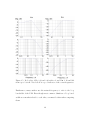
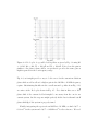
iteration of the system is assigned a revision letter. We describe these revisions in the paragraphs below. Table 4 summarizes the differences between
48
iterations.
trial
R13
C3
R17
R20
C1
R0
Offset
initial
A
B
C
150 kΩ
512 Ω
15 kΩ
15 kΩ
500 nF 500 nF 500 nF 500 nF
100 Ω
15 kΩ
15 kΩ
15 kΩ
200 Ω
1.5 kΩ
1.5 kΩ 1.5 kΩ
120 pF 120 pF 120 pF 120 pF
0Ω
100 kΩ 100 kΩ 100 kΩ
LM7905 LM7905 LM7905 Zener
E
15 kΩ
10 nF
15 kΩ
1.5 kΩ
120 pF
100 kΩ
Zener
F
15 kΩ
10 nF
15 kΩ
1.5 kΩ
1 nF
100 kΩ
Zener
Table 4.1: Modification of the tunable components for each revision.
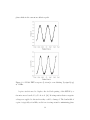
Revision A of the system involved a change of R13 to 512 Ω for a gain of
1 at U2A, R17 to 15 kΩ, R20 to 1.5 kΩ and R0 to 100 kΩ. The beat signal
power spectrum in a 1 MHz span for revision A of the system is shown in
Fig. 4.1. The current loop bandwidth at
50 kHz is clearly visible because of
the gain peaking phenomenon described in Sec. 2.1. Since the loop bandwidth
is small, it is not surprising that the OPLL cannot suppress phase noise efficiently, as evidenced by the amount of power in the sidebands of the carrier
frequency. Increasing the current gain potentiometer did not allow us to increase the loop bandwidth before the feedback started oscillating. Examining
the Bode plot of the current feedback phase advance filter in Fig. 3.10, we can
infer that by increasing the loop gain, we are essentially decreasing the gain
crossover frequency, which in turn drastically reduces phase margin if there is
a considerable phase shift in this path at frequencies below 1 MHz.
In order to increase the loop bandwidth without driving the OPLL into
oscillation, we increased the gain in the amplifier stage to 15 by setting R13
to 15 kΩ for revision B of the system. From the top plot in Fig. 4.1, a higher
49
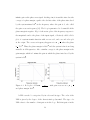
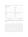
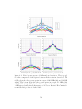
Figure 4.1: Plot of power spectra of different board revisions. The top plot
is for the comparison of the spectra between all the revisions described. The
middle plots show the power spectra in a span of 100 MHz (left) and 10 MHz
(right). The bottom plots show the power spectra in a span of 1 MHz (left)
and 200 kHz (right). All plots show the average of 40 traces, except for the
10 MHz traces which shows the average of 25 traces. Revision E is omitted in
the middle-left plot due to lack of data.
50
loop bandwidth is now achievable, which increased the performance of the
loop. At this point however, we noticed the system was highly susceptible to
noise, causing the loop to drift beyond capture range and unlock easily. Many
sources of electronic noise are contributing to the degraded performance of
the OPLL, but we chose to focus on the
5 V offset as noise introduced in
this section will be amplified more than any other noise in the feedback board.
Consequently, we changed the reference source to the zener diode of an LM399
precision reference. This improved the long-term stability of the loop and even
resulted in a slight improvement in the short-term stability in Fig. 4.1.
Since the system in revision C was still underperforming even within offset
frequencies of a few hundred kilohertz, it was clear that the piezo feedback loop,
which is most responsible for low frequencies, was not successfully correcting
for phase noise within its anticipated bandwidth. After a review of the transfer
function of the integrator in the piezo feedback path, Fig. 3.8, we hypothesized
that the performance in this path was being limited by the capacitor C3 and
an increase in its value would in turn increase the phase margin of the loop
and allow for better response in this path. Hence, for revision E we increased
C3 to 10 nF. The results are appreciable as shown in Fig. 4.1, where with the
same current loop bandwidth a much smaller noise floor is observed within the
couple hundred of kilohertz from the carrier frequency.
Note how the maximum current loop bandwidth did not change in this revision, since we only modified the piezo feedback path. For better performance
overall however, we must increase the current loop bandwidth, and it is clear
from our study of the current feedback path, in Sec. 3.3.2, that the phase shift
51
of the current modulation is preventing an increase of the loop bandwidth,
since it decreases the gain margin on this path, and restricts the current feedback from correcting phase noise at frequencies close to a hundred kilohertz.
For this reason, we attempt to modify the value of capacitor C1 as to tune the
transfer function of the filter to correct for the current modulation phase shift.
As we discussed in Sec. 3.3.2, we find the most suitable capacitance at this
point to be 1 nF. A considerable improvement can be seen for offset frequencies
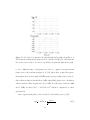
below 400 kHz, but a slight decline in performance is observed for higher offset
frequencies. Overall, revision F is still an improvement over revision E as the
power in the sidebands is significantly smaller. On the bottom-right panel of
Fig. 4.1, which spans only 200 kHz, the advantage of revision F is seen as the
carrier frequency contains a larger fraction of the total beat signal power.
Revision F is our final revision of the OPLL system as described in the
previous chapter. We also plot the revision F system with a smaller current
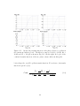
bandwidth in Fig. 4.1 for comparison, referred to as F1. This is clearly not the
best configuration for the system, but it does confirm our basic understanding
of the OPLL loop bandwidth and phase noise, i.e., noise outside the loop
bandwidth is not affected by the loop as illustrated in Fig. 2.5.
In order to characterize fully the final system’s stability, from which we
can make reasonable speculations about the success of using the system for
the Raman imaging transitions, we acquire the single-sideband (SSB) phase
noise spectra of the OPLL, shown in Fig. 4.2. We also plot the SSB phase noise
of the reference oscillator at 216 MHz in Fig. 4.3. These spectra are acquired by
the HP spectrum analyzer’s phase noise utility, which uses internal calibration
52
Figure 4.2: Phase noise spectra of the OPLL. Three distinct regions with
different slopes for the phase noise can be observed. We are mostly concerned
with the plateau region as it shows the loop needs improvement.
data to correct for error related to the detector’s voltage envelope and the
shape of bandwidth filter [29].
From the plot we see that flicker noise, with slope 1{fo , dominates offset frequencies above 100 kHz as expected from semiconductors in the board
[30]. Between 100 Hz and 10 kHz, the phase noise response is flat however,
indicating that either the current feedback path or the piezo feedback path is
not thoroughly correcting for phase error between these frequencies. A quick
glance at the Bode plot for the phase advance loop filter in the current feed53
Figure 4.3: Phase noise spectra of the reference.
back path, Fig. 3.10, shows that the gain sharply decreases for frequencies
below 1 MHz. We conclude that the current feedback loop must be further
optimized so as to correct for frequency perturbations at tens of kilohertz from
the carrier. If the gain of the path is such that the magnitude between 10 kHz
and 100 kHz of the overall current loop filter, shown in Fig. 3.12, is fully/partly
below zero, it is clear that the loop would have a problem minimizing phase
noise at these frequencies. This issue be avoided by modifying the resistance
in the phase-advance filter, effectively smoothing the bump seen at
3 MHz.
Another potential solution is to use a lead-lag filter, Bode plot shown in
54
Figure 4.4: Bode plot of a possible lead-lag filter as given by Eq. 3.2 using R1
= 3.8 kΩ, R2 = 300, C1 = 100 pF and C2 = 100 nF. Notice how the gain is
similar to the phase-advance filter, except that it provides the same gain as
high-frequencies in the low-frequency range.
Fig. 4.4, as it might provide a way to both correct for the current modulation
phase shift as well as allow for higher gain in the 100 Hz to 10 kHz frequency
regime. Substituting this filter in the overall current loop filter from Fig. 3.12,
we arrive at the Bode plot shown in Fig. 4.5. Note that in this case a 180
phase shift of the current feedback might be necessary from the one in our
current system, but the response might perfectly fit the laser’s thermal cutoff
phase shift flip if the system is properly tuned.
Finally, integrating the spectra from 100 Hz to 10 MHz, we find x∆φ2 y =
0.39 rad2 for the system and x∆φ2 y = 0.00014 rad2 for the reference. We need
55
Figure 4.5: Bode plot of current feedback path with lead-lag filter from Fig. 4.4.
The frequency independent gains are not combined in the plot, which means
the y-axes can be raised or lowered depending on gains throughout the path.
to set a different range of integration in order to compare our square-mean
phase error to the systems in Appel et al. [24], where they acquire the squaremean phase noise from a single 10 MHz span power spectrum of the beat note.
Since their resolution bandwidth is 3 kHz, their RMS phase noise calculation
will not include offset frequencies below 3 kHz. For the range between 3 kHz
and 3 MHz, we find x∆φ2 y = 0.155236 rad2 which is comparable to their
systems [24].
Since square-mean phase noise is related to the main power by [24]
@
expp ∆φ2
D
q ³8 Pcarrier
,
P pν qdν
8
56
(4.1)
and inputting the square-mean phase noise, we find that for the worst scenario
we will have at least 67.7 % of power at the carrier frequency, suggesting that
even at this stage we should be able to drive the Raman transitions with the
OPLL. Improvement of the loop should still be possible as discussed in this
section, and therefore better tuning of the current feedback path is advisable,
either through changing resistance of phase-advance filter, replacing the phaseadvance filter with a lead-lag filter and tuning it properly, or changing the
initial charge-pump loop filter to a second-order filter. Finally, even after the
changes to the 5 V offset source, the OPLL system seems susceptible to noise
and a thorough investigation of the feedback board might prove useful.
57
Chapter 5
Bragg-Raman Ultimate Laser
System
The OPLL is a small subset of a larger laser system dedicated to drive Bragg
and Raman transitions in
87
Rb BECs. Fig. 5.1 shows a diagram of the major
system, excluding the optics.
As we briefly mentioned in chapter 3, the current controller we use is a low
noise controller with large bandwidth, and it allows for digital programming of
the current using the Serial Peripheral Interface (SPI) protocol [31]. By placing
the controller close to the laser, we are minimizing the length of the cable
powering the diode and reducing susceptibility to noise. The current controller
box is small enough and can be conveniently placed on top of the ECDL
machined from the blueprints of Cook et al. [26]. Since the box is digitally
programmed, we minimize high-frequency noise in the injection current that
can increase phase noise in the laser beam.
58
Beat Signal
Photodiode
OPLL Box
PZT
Current Controller
Current
Mod
Laser
Digital Control Box
To BYU:
Digital Current Driver
Piezo Driver (Relayed from
OPLL)
Thermoelectric Cooler Driver
From BYU:
Current Monitor
Thermistor
Figure 5.1: Diagram of the Bragg-Raman laser system, divided into 4 essential
elements for each laser. The optics of the system are not shown.
A digital control box will contain the standard controls for our laser, which
includes temperature stabilization and digital current control. For the SPI
programming of the current controller box, we designed a microcontrollerbased interface that will be housed in the digital control box, see Appendix C.
Our OPLL box contains not only the control for the phase lock loop but
also a ramp generator to be used with the piezo when needed for scanning over
frequencies. A 10 Hz triangular wave is used for the ramp and it can be toggled
and adjusted using the same front panel controls as the OPLL. This ramp is
important when we want to make use of the spectroscopy techniques. Fig. 5.2
shows the layout of the physical OPLL box, which is currently in service.
59
Reference Signal
ADF4107
Board
CP
Signal Translator
Ramp Generator
Amplifiers
Directional
Coupler
To Current Mod
Board (MHz)
From
Photodiode
To Spectrum
Analyzer
To Piezo
Figure 5.2: Diagram of the OPLL box. This is the same box shown in Chapter
3 and we include a ramp generator on the feedback board as well as the power
supply for the ADF board, amplifiers and photodiode.
5.1
Optical Modules
We decided on a modular setup for the optical configuration. This allows us
to set up isolated portions of the optics connected through optical fibers. This
setup has the great advantage provided by any modular system wherein we
can modify a module without concern for the other modules of the system.
However, due to the power loss from coupling light into fibers, the setup cannot
contain be divided into an arbitrary number of modules linked by fibers. We
believe that in an optimization stage on the optics table we can bring the
coupling percentage to 80%, a reasonable value for fiber coupling. We therefore
divide our setup into three modules.
The master and slave module is shown in Fig. 5.3. Part of the laser beam
60
is coupled to a fiber to go to the Bragg-Raman module and another part is
used for saturated absorption spectroscopy. In the OPLL performance characterizations we did in Chapter 4, the master laser was always locked to a
transition in the Rb atom.
The polarizing beam splitter cube (PBSC), is similar to the BSC discussed
in Sec. 2.8, except that the percentage of beam power that goes through or
reflects at a right angle depends on the linear polarization of the beam, which
we control with a half-wave plate (HWP). This allows us to control the beam
power allocated for the saturated absorption spectroscopy and for coupling
into the fiber.
The Bragg-Raman module is the intermediary module receiving the master
and slave beams, preparing them for Bragg-Raman experiments, and taking
them to the condensate, as shown in Figs. 5.4 and 5.5. The top figure shows
the OPLL part of the setup, containing the Fabry-Perot and the photodiode
fiber coupler we discussed in Chapter 3. Here a half-wave plate allows control
over the beam power going to this section or to the output of this module. The
bottom figure shows each laser passing through an acousto-optic modulator
(AOM) before coupling into a fiber that will take it to the condensate. The
AOM will be necessary to set the detuning for the transition as discussed
by Thomas [9] and also to bring the beams to the exact frequency difference
necessary even though we will phase lock to 6.912 GHz. A removable mirror
allows different configurations of beams to enter the fibers on their way to
the condensate. The path shown is the one necessary for the desired Raman
transition.
61
PBSC
HWP
Optical
Isolator
Rb
Cell
Galilean
Telescope
Optical
Fiber
Photodiodes
Laser
Figure 5.3: Diagram of the master/slave module. The laser beam is split at
the PBSC, with part going to the saturated absorption spectroscopy and part
coupling to the fiber output of the module. By adjusting HWP, we can vary
the ratio of the beam power splittings at PBSC.
62
Figure 5.4: Picture of the Bragg-Raman module, showing mostly the OPLL
section of the optics.
63
Figure 5.5: Picture of the Bragg-Raman module, showing the beams passing
through AOMs and coupling into fibers that will the beams to the condensate.
64
Chapter 6
Conclusion
Although the Bragg-Raman transition system has not yet been fully implemented, we have made major contributions to its development. After choosing
to implement an OPLL synthesizer for an optical trap partial-transfer imaging
system, we developed the fundamental theory behind OPLLs and discussed the
challenges that surround its design.
We then designed and constructed the OPLL, which in its final revision
has a mean-square phase error of x∆φ2 y = 0.39. From this, we find that 67.7%
of the beat note’s power is in the carrier frequency, and thus the OPLL system
is likely be able to drive the desired stimulated Raman transitions. Finally we
briefly discussed how to further improve the system.
We recommended that the OPLL system be further improved before implementation since the overall system will greatly benefit from a more stable
loop. It is likely that spontaneous emission would be increased as a major result of the phase noise when driving the target imaging transition, since either:
65
the beams can be too unstable to drive enough transitions for a short pulse of
beams, thus requiring longer pulses or more power [9]; or the beams could be
unstable enough to drive unwanted transitions of the condensate.
Finally, we were able to picture the Bragg-Raman major system, design
and construct the OPLL box as described in chapter 5 and partially design
the other boxes of the system. We have written a program for a microcontroller
to take inputs from a rotary encoder, program the current controller board and
display to the user the current set in the current controller. The next step is to
continue building the digital control box, improve the OPLL’s performance,
bring the laser beams from the Bragg-Raman module to the BEC cell and
attempt to drive the desired Raman transitions.
66
Appendix A
OPLL System Schematics
67
Figure A.1: Simplified schematic of the Analog Devices evaluation board
adapted for use in our OPLL system [32]. For the reference input, we remove the 0 Ω bridges connecting the internal reference, R16, and the ADF’s
ref pin and also remove power to the reference, R14. To use the RFin port,
we replace R8, R9 and C17 with 0 Ω bridges and remove the link R7.
68
69
Figure A.2: Schematic of the phaselock electronics board, which contains the feedback processing of the OPLL.
Appendix B
Current Modulation
Figure B.1: Schematic of the current modulation board. The laser diode is
connected at TP3 and TP4 and the current controller at TP1 and TP2.
The current modulation board was adapted from Appel et al [24] and [33].
Through a modulation voltage at the input, we can control the current flowing
through the n-channel FET, allowing it to source or sink current from the laser
70
diode. Note that drain and source are interchangeable for this FET, allowing
our design to work with diodes of both orientations (anode and cathode).
71
Figure B.2: Front copper layer of the board sent for manufacturing.
72
Figure B.3: Back copper layer of the board sent for manufacturing.
73
Figure B.4: An unpopulated board next to a U.S. quarter dollar coin.
74
Figure B.5: The current modulation board connected to the laser diode and
sitting on a shelf inside the slave laser’s cavity. The board’s bottom and
sides are covered with hot-melt adhesive to insulate the solder joints from the
aluminum cavity and to provide stability
75
Appendix C
Digital Control
We designed a microcontroller-based solution for the programming of the current controller board, see Sec. 5. An ATmega328 microcontroller was used
for this board. The rotary encoder is attached to an external interrupt of the
microcontroller, allowing it to probe PB6 right away to check if the rotation
was clockwise or counterclockwise. A similar concept is used for reading out
the buttons. Each button press generates a hardware interrupt, which is when
the microcontroller reads the status of the buttons to discover which one was
pressed. An LED display provides messages to the user through a Universal
Asynchronous Receiver/Transmitter (UART) protocol.
76
Figure C.1: Digital control board schematic. Five buttons are assigned to a
directional joystick and the remaining button is just a standalone pushbutton
on the front panel.
77
Figure C.2: Picture of the working prototype without the button. The current
controller is shown in the left.
78
Bibliography
[1] M.H. Anderson, J. R. Ensher, M. R. Matthews, C.E. Wieman, and E. A.
Cornell. Observation of Bose-Einstein condensation in a dilute atomic
vapor. Science, 269:198, 1995.
[2] K. B. Davis, M.-O. Mewes, M. R. Andrews, N. J. van Druten, D. S.
Durfee, D. M. Kurn, and W. Ketterle. Bose-Einstein condensation in a
gas of sodium atoms. Phys. Rev. Lett., 75:3969, 1995.
[3] A. E. Leanhardt, Y. Shin, D. Kielpinski, D. E. Pritchard, and W. Ketterle.
Coreless vortex formation in a spinor Bose-Einstein Condensate. Phys.
Rev. Lett., 90:140403, 2003.
[4] T. Mizushima, K. Machida, and T. Kita. Mermin-Ho vortex in ferromagnetic spinor Bose-Einstein Condensate. Phys. Rev. Lett., 89:030401,
2002.
[5] Richard A. Battye, N. R. Cooper, and Paul M. Sutcliffe. Coreless vortex
formation in a spinor Bose-Einstein condensate. Phys. Rev. Lett., 88:
080401, 2002.
79
[6] Usama Al Khawaja and Henk Stoof. Skyrmions in a ferromagnetic BoseEinstein Condensate. Nature, 411:918, 2001.
[7] M. W. Ray, E. Ruokokoski, S. Kandel, M. M. Möttönen, and D. S. Hall.
Observation of Dirac monopoles in a synthetic magnetic field. Nature, 505
(7485):657660, January 2014. ISSN 1476-4687. doi: 10.1038/nature12954.
[8] D. V. Freilich, D. M. Bianchi, A. M. Kaufman, T. K. Langin, and D. S.
Hall. Real-time dynamics of single vortex lines and vortex dipoles in a
Bose-Einstein Condensate. Science, 329:1182, 2010. doi: 10.1126/science.
1191224.
[9] Nathan H. Thomas. Applications of stimulated raman scattering in BoseEinstein condensates. Undergraduate Thesis, Amherst College, 2013.
[10] B. J. Samelson-Jones. Vacuum Construction and Magneto-Optic Trapping for Bose-Einstein Condensation. Undergraduate Thesis, Amherst
College, 2001.
[11] S. F. Owen. Magnetic Trapping for Bose-Einstein Condensation of
87
Rb.
Undergraduate Thesis, Amherst College, 2002.
[12] T. J. Reber. Creating and Optically Trapping a Bose-Einstein Condensate
in Rubidium 87. Undergraduate Thesis, Amherst College, 2003.
[13] J. Merrill. Characterization of Inelastic Losses from Bose-Einstein Condensates in the |2, 1y State of
87
Rb. Undergraduate Thesis, Amherst Col-
lege, 2006.
80
[14] D. H. Guest. A Cross-Beam Far Off-Resonance Optical Trap for
Bose-Einstein Condensates.
87
Rb
Undergraduate Thesis, Amherst College,
2006.
[15] Joshua Hughes and Chad Fertig. A widely tunable laser frequency offset lock with digital counting. Review of Scientific Instruments, 79(10):
103104, 2008. ISSN 0034-6748. doi: 10.1063/1.2999544.
[16] Alberto M. Marino and C. R. Stroud. Phase-locked laser system for use
in atomic coherence experiments. Review of Scientific Instruments, 79(1):
013104, 2008. ISSN 0034-6748. doi: 10.1063/1.2823330.
[17] Melanie Müller. Realization of a laser system for coherent spectroscopy
of fiber-coupled cesium atoms. Master’s thesis, Johannes GutenbergUniversitt Mainz, 2010.
[18] G. Santarelli, A. Clairon, S.N. Lea, and G.M. Tino. Heterodyne optical
phase-locking of extended-cavity semiconductor lasers at 9 GHz. Optics
Communications, 104(4-6):339344, Jan 1994. ISSN 0030-4018. doi: 10.
1016/0030-4018(94)90567-3.
[19] Th. Udem, A. Huber, B. Gross, J. Reichert, M. Prevedelli, M. Weitz,
and T. Hnsch. Phase-coherent measurement of the hydrogen 1S-2S transition frequency with an optical frequency interval divider chain. Physical Review Letters, 79(14):26462649, Oct 1997. ISSN 1079-7114. doi:
10.1103/physrevlett.79.2646.
81
[20] Floyd M. Gardner. Phaselock Techniques. Wiley-Interscience, 2005. ISBN
0471430633.
[21] Panos J. Antsaklis and Anthony N. Michel. Linear Systems. Birkhäuser,
2005. ISBN 0817644342.
[22] Mike Curtin and Paul O’Brien. Phase-locked loops for high-frequency
receivers and transmitters—part 1. Analog Dialogue, 33(7):1–5, 1999.
[23] Norman S. Nise. Control Systems Engineering, 5th Edition. Wiley, 2007.
ISBN 9780471794752.
[24] Jürgen Appel, Andrew MacRae, and A I Lvovsky. A versatile digital
ghz phase lock for external cavity diode lasers. Measurement Science
and Technology, 20(5):055302, May 2009. doi: 10.1088/0957-0233/20/5/
055302.
[25] E. A. Donley, T. P. Heavner, F. Levi, M. O. Tataw, and S. R. Jefferts.
Double-pass acousto-optic modulator system. Review of Scientific Instruments, 76(6):063112, 2005. ISSN 0034-6748. doi: 10.1063/1.1930095.
[26] Eryn C. Cook, Paul J. Martin, Tobias L. Brown-Heft, Jeffrey C. Garman,
and Daniel A. Steck. High passive-stability diode-laser design for use
in atomic-physics experiments. Review of Scientific Instruments, 83(4):
043101, 2012. ISSN 0034-6748. doi: 10.1063/1.3698003.
[27] Daniel A. Steck. Rubidium 87 d line data. URL http://steck.us/
alkalidata. (revision 2.0.1, 2 May 2008).
82
[28] Analog Devices. Adf4107 user manual, .
[29] Agilent Technologies. Agilent 85671a phase noise measurements utility.
URL http://cp.literature.agilent.com/litweb/pdf/5091-7089E.
pdf.
[30] Mike Curtin and Paul O’Brien. Phase-locked loops for high-frequency
receivers and transmitters—part 2. Analog Dialogue, 33(5):1–4, 1999.
[31] Christopher J. Erickson, Marshall Van Zijll, Greg Doermann, and
Dallin S. Durfee. An ultrahigh stability, low-noise laser current driver
with digital control. Review of Scientific Instruments, 79(7):073107, 2008.
ISSN 0034-6748. doi: 10.1063/1.2953597.
[32] Analog Devices. EV-adf411xsd1z user guide, .
[33] Toptica
100.
Photonics.
URL
Part
iv
diode
laser
head
DL
http://web.mit.edu/8.13/8.13d/manuals/
tui-dl100-laser-system-dec01-mit-junior-lab-part-p3.pdf.
83