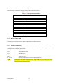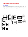
1
WESTERN AVIONICS
MIL-STD-1553B PCI
INTELLIGENT INTERFACE BOARD
P/N 1U10928G01 Rev B
User Manual
UM 10928 Rev B
© Western Avionics Ltd.
13/14 Shannon Free Zone
Co. Clare
Ireland
7 February 2001
Table of Contents
1
GENERAL INFORMATION ............................................................................................................................ 6
1.1
INTRODUCTION ........................................................................................................................................ 6
1.2
MANUAL DESCRIPTION .......................................................................................................................... 6
1.3
CAPABILITIES............................................................................................................................................ 6
1.3.1
General.................................................................................................................................................. 6
1.3.2
Bus Controller (BC) Features (With MRT Simulation and Data Monitoring) ...................................... 7
1.3.3
Multiple Remote Terminal (MRT) Features .......................................................................................... 7
1.3.4
Chronological Bus Monitor (CM) Features.......................................................................................... 7
1.4
THE IIB-1553-PCI ARCHITECTURE.......................................................................................................... 8
1.5
PROTOCOL MANAGEMENT UNIT ......................................................................................................... 8
1.6
1553B INTERFACE ..................................................................................................................................... 8
1.7
FEATURES .................................................................................................................................................. 9
1.8
SYSTEM CHARACTERISTICS AND SPECIFICATIONS........................................................................ 9
1.9
LIST 0F FURNISHED ITEMS................................................................................................................... 10
1.10 LIST 0F RELATED PUBLICATIONS ...................................................................................................... 10
1.11 STORAGE DATA ...................................................................................................................................... 10
1.12 TOOLS AND TEST EQUIPMENT............................................................................................................ 10
1.13 SAFETY PRECAUTIONS ......................................................................................................................... 10
2
INSTALLATION AND PREPARATION FOR USE..................................................................................... 12
2.1
GENERAL .................................................................................................................................................. 12
2.2
INSTALLATION OF THE IIB-1553-PCI................................................................................................. 12
2.3
TURN ON ................................................................................................................................................... 12
2.4
RESET ........................................................................................................................................................ 12
2.5
SPECIFIC FEATURES............................................................................................................................... 13
2.5.1
Control Register Features................................................................................................................... 13
2.5.2
Counter Features ................................................................................................................................ 13
2.5.3
Trigger-In Features............................................................................................................................. 13
2.5.4
Trigger Out Features .......................................................................................................................... 13
2.6
PCI INTERFACE........................................................................................................................................ 14
2.6.1
Introduction......................................................................................................................................... 14
2.6.2
Electrical Characteristics.................................................................................................................... 14
2.6.3
Capabilities ......................................................................................................................................... 14
2.7
1553B INTERFACE ................................................................................................................................... 14
2.7.1
lntroduction......................................................................................................................................... 14
2.7.2
Electrical Characteristics.................................................................................................................... 14
2.8
PINOUTS.................................................................................................................................................... 15
3
OPERATION .................................................................................................................................................... 16
3.1
INTRODUCTION ...................................................................................................................................... 16
3.2
CONVENTIONS ........................................................................................................................................ 16
3.3
ORGANISATION DIAGRAM................................................................................................................... 16
3.4
BASE REGISTERS .................................................................................................................................... 16
3.4.1
Base Register Names and Locations ................................................................................................... 18
3.4.2
Base Register Descriptions ................................................................................................................. 19
3.4.2.1
3.4.2.2
3.4.2.3
3.4.2.4
3.4.2.5
U
U
M
R
B
UM
M 111000999222888 R
Reeevvv B
B
Control Register (Write) (00H) ........................................................................................................................19
Clock Hl Word (Read) (00H) (Clock LO Word (Read) (02H) .........................................................................19
Command Register (CR) (04H)........................................................................................................................20
Status Register (SR) (06H) ...............................................................................................................................21
Background Running Pointer (BRP) (08H)......................................................................................................22
-2-
3.4.2.6
3.4.2.7
3.4.2.8
3.4.2.9
3.4.2.10
3.4.2.11
3.4.2.12
3.4.2.13
3.4.2.14
3.4.2.15
3.4.2.16
3.4.2.17
3.4.2.18
3.4.2.19
3.4.2.20
3.4.2.21
3.4.2.22
3.4.2.23
3.4.2.24
3.4.2.25
3.4.2.26
Insertion Running Pointer (IRP) (OAH) ..........................................................................................................24
Reserved (0CH) ................................................................................................................................................24
LPIQAP (0EH) Low priority interrupt queue start address. .............................................................................24
Reserved (10H).................................................................................................................................................24
HPIQAP (12H) High priority interrupt queue start address. ........................................................................24
Reserved (14H) ............................................................................................................................................24
MIQAP (16H) Message interrupt queue start address.................................................................................24
Reserved (18H) ............................................................................................................................................24
SRQAP (lAH) Status report queue start address.........................................................................................24
Reserved (lCH) ............................................................................................................................................24
RTSTAD (lEH) RT simulation table start address. .....................................................................................24
Reserved (20H) ............................................................................................................................................24
Reserved (22H) ............................................................................................................................................24
Toggle Buffer Address Offset (24H)............................................................................................................25
Set of Messages Start Address (26H)...........................................................................................................25
Global RT Response Time Register (28H)...................................................................................................25
RT No Response Time-Out Register (2AH) ................................................................................................25
IRQ Selection Register (34H) ......................................................................................................................26
Test and Set Register and SRQADP (3CH) .................................................................................................26
Reserved (46H) ............................................................................................................................................27
PRI/SEC 1553B RT TX Inhibit HI-LO (48H – 4EH)..................................................................................27
3.5
REMOTE TERMINAL SIMULATION TABLE ....................................................................................... 28
3.5.1
Simulation Type Word......................................................................................................................... 28
3.5.2
Status Word ......................................................................................................................................... 29
3.5.3
1553B Last Command Word ............................................................................................................... 29
3.5.4
1553B Bit Word................................................................................................................................... 29
4
BUS CONTROLLER MODE OF OPERATION........................................................................................... 30
4.1
INTRODUCTION ...................................................................................................................................... 30
4.2
MESSAGE DESCRIPTOR BLOCK (MDB).............................................................................................. 31
4.2.1
Message Number (00H) ...................................................................................................................... 31
4.2.2
1553B Event Mask (02H) .................................................................................................................... 31
4.2.3
Message Type Word (04H).................................................................................................................. 32
4.2.4
1553B Message Error Phase Definition (06H) ................................................................................... 33
4.2.5
1553B Message Error Description Word (08H) ................................................................................. 33
4.2.6
Address in Look-Up Table (0AH)........................................................................................................ 34
4.2.7
Command Word 1 (0CH) .................................................................................................................... 34
4.2.8
Command Word 2 (0EH)..................................................................................................................... 34
4.2.9
Retry Subroutine Absolute Address (14H) .......................................................................................... 34
4.2.10 Inter-message Gap Time (18H)........................................................................................................... 35
4.2.11 Status Word 1 (lCH)............................................................................................................................ 35
4.2.12 Status Word 2 (lEH) ............................................................................................................................ 35
4.3
DATA BUFFERS SIMULATION AND MONITORING.......................................................................... 36
4.3.1
Look-Up-Table .................................................................................................................................... 37
4.3.2
Data Descriptor Block ........................................................................................................................ 37
4.3.2.1
4.3.2.2
4.3.2.3
4.3.2.4
4.3.2.5
4.3.2.6
Option Mask (00H) ..........................................................................................................................................38
Data Status Report (06H) .................................................................................................................................38
Toggle Frequency and Buffer Address HI (08H) .............................................................................................38
Link Pointer to New DDB (0CH).....................................................................................................................39
Address of Modify Word/Value to Write (0EH-l0H) .......................................................................................39
Extended Sub-Address .....................................................................................................................................40
4.3.3
Data Buffers ........................................................................................................................................ 40
4.4
MODE COMMANDS................................................................................................................................. 41
4.5
INTERRUPT REQUESTS.......................................................................................................................... 42
4.5.1
Interrupt Coding ................................................................................................................................. 42
4.5.2
Set Message Interrupts ........................................................................................................................ 42
4.5.3
Message Status Report Queue............................................................................................................. 43
U
U
M
R
B
UM
M 111000999222888 R
Reeevvv B
B
-3-
5
MULTIPLE REMOTE TERMINAL MODE OF OPERATION ................................................................. 44
5.1
INTRODUCTION ...................................................................................................................................... 44
5.2
LOOK-UP-TABLES................................................................................................................................... 45
5.3
MODE COMMANDS SPECIFICATIONS ................................................................................................ 45
5.4
DATA WORDS STORAGE ....................................................................................................................... 45
5.5
1553B ERROR INJECTION DEFINITION............................................................................................... 45
5.5.1
Global RT Error Description Word (RT Simulation Table)................................................................ 46
5.5.2
Message Error Injection Word (Look-up-Table)................................................................................. 47
5.6
INTERRUPTS CODING ............................................................................................................................ 48
5.6.1
Low and High Priority Interrupts (two word code) ............................................................................ 48
5.6.2
Message lnterrupts (or set of messages interrupt) .............................................................................. 48
5.6.3
Status Report Queue (two words per report) ...................................................................................... 48
5.7
SPECIFIC FUNCTIONS ............................................................................................................................ 48
5.7.1
Data Message Reception..................................................................................................................... 48
5.7.2
Reception of Mode Commands Data Words ....................................................................................... 48
5.7.3
Mode Command "Synchronise with Data Word"................................................................................ 49
5.7.4
Frequency Toggle ............................................................................................................................... 49
6
CHRONOLOGICAL BUS MONITOR MODE OF OPERATION ............................................................. 50
6.1
INTRODUCTION ...................................................................................................................................... 50
6.2
BASE REGISTERS .................................................................................................................................... 50
6.2.1
Control Register (Write) (00H) ........................................................................................................... 51
6.2.2
Command Register (CR) ..................................................................................................................... 51
6.2.3
Status Register (SR)............................................................................................................................. 52
6.2.4
IRQ Selection Register (34H).............................................................................................................. 52
6.2.5
Load Clock HI/LO Registers (+38H1 / +3AH)................................................................................... 53
6.2.6
Current Address Register (CAR) (+42H)............................................................................................ 53
6.2.7
Trigger Occurrence Register (TOR) (+44H) ...................................................................................... 53
6.2.8
Trigger Set-up Pointer (TSP) (+46H) ................................................................................................. 53
6.2.8.1
Trigger Set-up Data ..........................................................................................................................................53
6.3
DETAILED TRIGGER DESCRIPTION.................................................................................................... 54
6.4
STACK DATA FORMAT .......................................................................................................................... 64
6.4.1
Previous Address Pointer.................................................................................................................... 64
6.4.2
Time Stamp HI/LO .............................................................................................................................. 64
6.4.3
Data..................................................................................................................................................... 64
6.4.4
Next Address Pointer........................................................................................................................... 65
6.4.5
RT Response Time 1/2 ......................................................................................................................... 65
6.4.6
Flow Diagram ..................................................................................................................................... 65
U
U
M
R
B
UM
M 111000999222888 R
Reeevvv B
B
-4-
List of Figures
Figure 1-1.
Figure 1-2.
Figure 2-3.
Figure 3-2.
Figure 4-1
Figure 4-2.
Figure 5-1.
IIB-1553-PCI Functional Block Diagram................................................................................................ 8
IIB-1553-PCI Front Panel ..................................................................................................................... 11
Trig IN/OUT Pin Orientation ................................................................................................................ 15
Remote Terminal Simulation Table....................................................................................................... 28
Bus Controller Organisation Diagram ................................................................................................... 30
Data Buffers Simulation and Monitoring............................................................................................... 36
Multiple Remote Terminal Organisation Diagram ................................................................................ 44
List of Tables
Table 2-1.
Table 3-1.
Table 3-2.
Table 3-3.
Table 4-1.
Table 4-2.
Table 4-3.
Table 6-1.
Table 6-2.
Table 6-3.
Table 6-4.
Trig-In / Trig-Out Connectors Pinouts.................................................................................................... 15
Base Register Names and Locations........................................................................................................ 18
Command Register (CR).......................................................................................................................... 20
Status Register ......................................................................................................................................... 21
Message Descriptor Block....................................................................................................................... 31
Data Descriptor Block ............................................................................................................................. 37
Data Buffers............................................................................................................................................. 41
Base Registers.......................................................................................................................................... 50
Command Registers ................................................................................................................................. 51
Status Registers........................................................................................................................................ 52
Stack Data Format ................................................................................................................................... 64
U
U
M
R
B
UM
M 111000999222888 R
Reeevvv B
B
-5-
1
1 .1
GENERAL INFORMATION
INTRODUCTION
The Western Avionics IIB-1553-PCI Intelligent Interface Board is a standard PCI card designed to meet the requirements
of MIL-STD-1553B and STANAG 3838. The Western Avionics IIB-1553-PCI provides a powerful and intelligent
interface between a PCI based host equipment and the 1553B data bus. Bus Controller and Multi-Remote Terminal
functions can operate both independently or simultaneously. An additional independent Chronological Bus Monitor
function is provided. The Western Avionics IIB-1553-PCI provides complete and comprehensive test and simulation
functions for all applications in MIL-STD-1553B systems.
1 .2
MANUAL DESCRIPTION
The following paragraphs provide a general description of the manual layout and content:
•
Section 1
General Information - contains a brief description of the manual, and a general description
of the Western Avionics IIB-1553-PCI. This section also contains the architecture,
protocol management, MIL-STD-1553B interface information, instrument specifications,
information concerning accessories, furnished items and also safety precautions.
•
Section 2
Installation and Preparation for Use - contains instructions on installation, preparation for use,
self-test and reset of the Western Avionics IIB-1553-PCI card.
•
Section 3
Operation - contains a functional description of the Western Avionics IIB-1553-PCI and
operating procedures necessary to run the card.
•
Section 4
Bus Controller Mode of Operation - contains information on the mode of operation for the Bus
Controller function of the Western Avionics IIB-1553-PCI card.
•
Section 5
Multiple Remote Terminal Mode of Operation - contains information on the mode of
operation for the Multiple Remote Terminal function of the Western Avionics IIB-1553-PCI
card.
•
Section 6
Chronological Bus Monitor Mode of Operation - contains information on the mode of
operation for the Chronological Bus Monitor function of the Western Avionics IIB-1553-PCI
card.
1 .3
CAPABILITIES
The Western Avionics IIB-1553-PCI provides the following capabilities and functions:
1 .3 .1
General
•
•
•
•
•
•
•
•
U
U
M
R
B
UM
M 111000999222888 R
Reeevvv B
B
Memory mapped real-time universal PCI interface.
2MByte of RAM.
INTA interrupt.
1553B data protocol managed by a micro-controller providing
flexibility and extensibility.
Comprehensive Error Injection.
External Triggers.
Internal Self-tests.
Standard single PCI card format.
-6-
1 .3 .2
Bus Controller (BC) Features (With MRT Simulation and Data Monitoring)
•
Bus Control:
• Autonomous frame control using comprehensive set of instructions
and message descriptor blocks.
• Acyclic message insertion.
• Error injection.
• Frame frequency selection.
• Inter-message gap selection.
• Response time-out selection.
• Bus events detection, mask, storage, and reporting (bus errors, status word bits).
•
•
Simultaneous MRT Simulation (up to 31).
Data Words Transfers:
•
•
•
•
1 .3 .3
Simultaneous monitoring of all data buffers.
Multiple Remote Terminal (MRT) Features
•
Simulation:
•
•
•
•
Up to 31 1553B - RT simulations.
Mode and Broadcast commands handling.
Comprehensive Error Injection.
Data Words Transfers:
•
•
•
1 .3 .4
Data buffer simulation for the BC and the simulated RT's.
Sub-address based data buffer access with data descriptor blocks defining each bus
message;
•
Multi-buffering (linked buffers or frequency-toggled buffers).
•
Interrupt queues.
•
Data status report.
Data buffer time tagging (32 bits time tag).
Data buffer simulation for simulated RTs.
Sub-address based data buffer access offering the same powerful data buffering as in the
bus controller mode.
All non-transmitted data messages are monitored.
Chronological Bus Monitor (CM) Features
•
Capture of all bus activity in chronological stack, with time tagging of each message.
•
Comprehensive multi-trigger facilities allowing selective capture and interrupts to be performed
on complex data sequence.
•
Cyclical stack up to 2Mbyte, with interrupt on completion of capture.
•
All 1553B errors detected.
U
U
M
R
B
UM
M 111000999222888 R
Reeevvv B
B
-7-
1 .4
The IIB-1553-PCI ARCHITECTURE
The Western Avionics IIB-1553-PCI board is a memory mapped PCI MIL-STD-1553B interface with high performance
architecture and complex features. Placed in a 3.3V or +5V PCI slot (universal) the IIB-1553-PCI card provides
enhanced test and simulation functions for all modes of operation of a MIL-STD-1553B bus. The host equipment, using
the on-board RAM, defines all configuration and data structures.
Protocol
UNIVERSAL
PCI
INTERFACE
2 Meg
Management
RAM
Unit
1553B
INTERFACE
1553B Lines in/out
INTERRUPT
Figure 1-1.
IIB-1553-PCI Functional Block Diagram
1 .5
PROTOCOL MANAGEMENT UNIT
A micro-controller based structure running at 40Mhz handles the management of the 1553B protocol for each of the
operating modes (BC, MRT, BM). The micro-controller works each of the 1553B command, status and data words
functions of its operating mode and the configuration tables in RAM. The micro-controller management unit allows
flexibility and expandability for the bus control tasks and user interface.
1 .6
1553B INTERFACE
The 1553B interface is a dual redundant interface, which includes a standard dual redundant transceiver and a Manchester
encoder/decoder with full error detection and error injection capabilities, which include:
•
•
•
•
•
•
•
U
U
M
R
B
UM
M 111000999222888 R
Reeevvv B
B
Manchester bit error
Synch bit error
Parity error
Word length error
Wrong bus error
Both bus error
Response time error
-8-
1 .7
FEATURES
The features of the Western Avionics IIB-1553-PCI are listed as follows:
•
Universal PCI card.
•
Memory mapped real-time PCI interface.
•
2MByte of RAM.
•
Multiple interrupt queues for various events.
•
1553B data protocol managed by a micro-controller providing complete flexibility and
extension capability.
•
Error Injection and detection.
•
External Triggers.
•
Internal Self-tests.
1 .8
SYSTEM CHARACTERISTICS AND SPECIFICATIONS
The characteristics and specifications of the Western Avionics IIB-1553-PCI are listed as follows:
•
Size:
Standard PCI card (175 by 107 mm)
•
Power
+5Vdc @ 600 mAmps
+12Vdc @ 160mAmps
•
Temperature:
• Operating:
• Non-operating:
•
0°C to +50°C
-20°C to +70°C
MTBF:
• 104,817 Hrs (Ground Benign @ 25°C)
• Front Panel Connectors:
• Trig-In/Trig-Out:
• Two tri-axial:
U
U
M
R
B
UM
M 111000999222888 R
Reeevvv B
B
[J3, 9 Pin sub-miniature D type, M2408/23-31]
[J1, 1553B Primary triaxial, type CBBJR79]
[J2, 1553B Secondary triaxial, type CBBJR79]
-9-
1 .9
LIST 0F FURNISHED ITEMS
The following is a list of furnished items:
1. Bus Analyser/Simulator, Model IIB-1553-PCI
2. Users Manual UM 10928 (This document)
1 .1 0
LIST 0F RELATED PUBLICATIONS
The following is a list of related publications:
1.
2.
MIL-STD-1553
PCI LOCAL BUS specification
1.11 STORAGE DATA
As the PC card contains electrostatic sensitive devices (ESD's), special storage and handling is required.
Do not store near electrostatic, electromagnetic, magnetic or radiation fields.
1.12 TOOLS AND TEST EQUIPMENT
No special tools or test equipment is required to test the Western Avionics IIB-1553-PCI
1 .1 3
SAFETY PRECAUTIONS
WARNING
Potentially hazardous voltages exist on the host computer power supply.
Do not attempt to install or remove the Western Avionics IIB-1553-PCI without first
removing main power. Improper handling can cause injury or death.
U
U
M
R
B
UM
M 111000999222888 R
Reeevvv B
B
- 10 -
J1
1553B PRIMARY
J2
1553B SECONDARY
J3
TRIG IN / TRIG OUT
Figure 1-2.
U
U
M
R
B
UM
M 111000999222888 R
Reeevvv B
B
IIB-1553-PCI Front Panel
- 11 -
2
INSTALLATION AND PREPARATION FOR USE
2 .1
GENERAL
On delivery, inspect the unit for possible damage. If it is damaged, notify the shipping company, and contact your
distributor, or the Western Avionics, for details of return procedure. When unpacking remove all protective covering and
store covering and packing container, as unit may need to be reshipped at a later date.
CAUTION
The IIB-1553-PCI card contains Electrostatic Sensitive Devices (ESD's).
Observe ESD handling requirements, and do not ship or store near
electro-static, electromagnetic, magnetic or radioactive fields.
2 .2
INSTALLATION OF THE IIB-1553-PCI
Prior to installing the Western Avionics IIB-1553-PCI, ensure that all power has been removed from the host computer.
2 .3
TURN ON
Set mains power on host computer to ON. The Western Avionics IIB-1553-PCI will perform system self-test on the BC,
MRT and CM lasting approximately four seconds.
2 .4
RESET
The Western Avionics IIB-1553-PCI hardware and firmware are reset as follows:
Reset:
• Signal #RES from the PCI bus.
• Power-up and power-down.
• Bit location in control register accessible by the PCI interface.
U
U
M
R
B
UM
M 111000999222888 R
Reeevvv B
B
- 12 -
2 .5
SPECIFIC FEATURES
2 .5 .1
Control Register Features
This is a 16-bit write only register accessible from the PCI bus.
This register is mapped into the memory field. The features are as follows:
• Hardware reset
• Three prioritised interrupts to the local on-board processor for indication and control
• Acknowledge PCI Interrupt
2 .5 .2
Counter Features
This 32-bit counter is a free running counter with a 0.5µs or l0µs LSB and can be read from a memory mapped location
via the PCI bus interface. The counter should be read in a single 32-bit access. The counter can be updated and used by
the on-board processor as follows•
Used:
Data buffers time tagging
Frame cycles control
Bus Monitoring
•
Updated:
User request
1553B command
2 .5 .3
Trigger-In Features
Trigger-In enters the board logic through a 9-way socket connector and then an opto-coupler. Inputs to this feature can be
used for hardware starts of the major and/or minor frames, or external trigger for the bus monitor.
2 .5 .4
Trigger Out Features
Trigger-Out is in fact a bit in a register accessible by the on-board processor to indicate to the external world that an event
has been detected. This event can be as follows:
•
•
•
Beginning of the major and/or minor frames
Beginning of a message
Bus Monitor trigger detected
Trigger-Out exits the board through an opto-coupler and a nine-way socket connector on the front panel.
U
U
M
R
B
UM
M 111000999222888 R
Reeevvv B
B
- 13 -
2 .6
PCI INTERFACE
2 .6 .1
Introduction
The PCI interface on the Western Avionics IIB-1553-PCI board conforms to PCI LOCAL BUS specification Rev 2.2
2 .6 .2
Electrical Characteristics
•
+5V and +12V.
•
All driving and loading rules are respected.
2 .6 .3
Capabilities
The Western Avionics IIB-1553-PCI board is used as a 2Mbyte field.
•
•
•
2 .7
R/W Static RAM (2Mbyte).
Read only 32-bit counter (one 32-bit access)
Write only 16-bit register (one 16-bit access).
1553B INTERFACE
2 .7 .1
lntroduction
The 1553B interface matches the MIL-STD-1553B Standard.
2 .7 .2
Electrical Characteristics
The 1553B interface provides one dual redundant bus.
• Primary bus.
• Secondary bus.
The 1553B interface can be programmed to be:
• Transformer coupled.
• Direct coupled.
U
U
M
R
B
UM
M 111000999222888 R
Reeevvv B
B
- 14 -
2 .8
PINOUTS
J1 and J2 (1553 Primary and 1553 Secondary) are wired with positive going signal on inner conductor, and negative
going signal on outer, with ground on connector body.
J3 is wired as below:
Table 2-1. Trig-In / Trig-Out Connectors Pinouts (J3)
PIN NUMBER
1
2
3
4
5
6
7
8
9
DESCRIPTION
1553 Primary positive
1553 Secondary positive
Trig Out, Opto-coupler Collector
Trig In, Opto-coupler Cathode
Ground
1553 Primary negative
1553 Secondary negative
Trig Out, Opto-coupler Emitter
Trig In, Opto-coupler Anode
5
9
6
1
Figure 2-3. Trig IN/OUT Pin Orientation (J3)
U
U
M
R
B
UM
M 111000999222888 R
Reeevvv B
B
- 15 -
3
OPERATION
3 .1
INTRODUCTION
The Western Avionics IIB-1553-PCI Intelligent Interface Board provides Bus Controller (BC), Multi-Remote Terminal
(MRT), functions, which may be run either independently or simultaneously. An independent Chronological Bus Monitor
(CM) is also provided. In order to run any of these functions, information must be loaded into specific fixed register
locations (Base Registers). Some of these registers contain pointers to other areas of memory/registers. The selection of
these pointers is left up to the discretion of the user. Therefore, memory blocks can be positioned in the on-board memory
to suit user requirements. This set-up means that fixed position registers are minimal.
3 .2
CONVENTIONS
1.
BASE = PCI Base Address of this board.
2.
The memory range BASE+l0000H to End of Memory is reserved for the
1553B data blocks. All other data must reside in the first 64Kbytes.
After a Power-On:
•
•
On-board processor doing its power-on initialisation,
•
Then executing Self-Test.
•
Then waiting for a user command.
DSI per default (insertion program is disabled)
3 .3
ORGANISATION DIAGRAM
The organisation diagram figure 3-1 shows how the functional areas of the Western Avionics IIB-1553-PCI board can be
controlled.
3 .4
BASE REGISTERS
The only fixed position registers are the Base Registers. The Base Registers are the starting points for a description of
operation of any of the three modes of operation, (BC, MRT and CM).
They are located starting at the board Base Address.
U
U
M
R
B
UM
M 111000999222888 R
Reeevvv B
B
- 16 -
BC/MRT
BC
MRT
Background Program
Area
1553B LUT
Reserved MRT
DDB Address
Address in LUT
SMB
BASE REGISTER
Message Descriptor
Block
Message Number
DATA BUFFERS
Time Tag HI
Time Tag LO
Data
BRP
IRP
DDB
Options mask
Insertion
Program
Queues Address
Data buffer Address HI
Data buffer Address LO
RTSTAD
1553 LUT
High
Priority
Interrupt
Message
Status
Report
RT1
RT30
RT30
Figure 3-1
U
U
M
R
B
UM
M 111000999222888 R
Reeevvv B
B
DDB
Options mask
Data buffer Address HI
Data buffer Address LO
RT1
Message
Interrupt
Error Injection
Word
DDB Address
TX
Low
Priority
Interrupt
1553B LUT
Address
DATA BUFFERS
RX
RT0
RT Simulation Table
Organisation Diagram
- 17 -
Time Tag HI
Time Tag LO
Data
3 .4 .1
Base Register Names and Locations
The names and locations of the Base Registers are contained in table 3-1.
Table 3-1. Base Register Names and Locations
BASE
+02H
+04H
+06H
+08H
+0AH
+0CH
+0EH
+l0H
+12H
+14H
+16H
+18H
+lAH
+lCH
+lEH
+20H
+22H
+24H
+26H
+28H
+2AH
+2CH
+2EH
+30H
+32H
+34H
+36H
+38H
+3AH
+3CH
+3EH
+40H
+42H
+44H
+46H
+48H
+4AH
+4CH
+4EH
+50H
+52H
+54H
+56H
U
U
M
R
B
UM
M 111000999222888 R
Reeevvv B
B
Control Register(Write)/Clock HI Word (Read)
Clock LO Word (Read only)
Command Register (CR)
Status Register (SR)
Background Running Pointer (BRP) Address of Program
Insertion Running Pointer (IRP) Address of Program
Reserved
Low Priority Interrupt Queue Start Address Pointer
Reserved
High Priority Interrupt Queue Start Address Pointer
Reserved
Message Interrupt Queue Start Address Pointer
Reserved
Status Report Queue Start Address Pointer
Reserved
RT Simulation Table Address Register (RTSTAD)
Amplitude Register
Coupling Register
Toggle Buffer Address Offset (MSB=l Global Enable)
SET OF MESSAGES Start Address
Global RT Response Time Register (µs)
RT No Response Timeout Register (µs)
Reserved
Reserved
Reserved
Reserved
IRQ Selection Register
Minor Frame Counter Register
Load Clock Hl Register
Load Clock LO Register
Test and Set register (TASR)
Service Request Queue Address Pointer (SRQADSP)
Cycling Interrupt Update Register
Monitor Current Address Register (CAR)
Monitor Trigger Occurrence Register (TOR)
Monitor Trigger Set-up Pointer (TSP)
PRI Bus 1553B RT TX inhibit bits Hl
PRI Bus 1553B RT TX inhibit bits LO
SEC Bus 1553B RT TX inhibit bits Hl
SEC Bus 1553B RT TX inhibit bits LO
Reserved
Reserved
Reserved
Reserved
- 18 -
3 .4 .2
Base Register Descriptions
The Base Register functions are defined in the following paragraphs.
3.4.2.1
D15
0
Control Register (Write) (00H)
D14
0
D13
0
D12
0
C0
Cl
HR
D11
0
Clear
Clear
Clear
D10
0
=>
=>
=>
D09
0
D08
HR
D07
0
D06
IEN
D05
IRQ
D04
0
D03
0
D02
0
D01
C1
Command Request
Insertion Request
Hardware RESET
If IEN is set and IRQ is set then interrupt line will be cleared.
If IEN is set and IRQ is clear then the interrupt line will be asserted (for test purposes only).
If IEN is clear the value of IRQ is unaffected.
Note: This register must be accessed to clear the interrupt during an interrupt service routine.
Examples:
3.4.2.2
1. 0102H generates a command request.
2. 0163H clears the interrupt line.
Clock Hl Word (Read) (00H) (Clock LO Word (Read) (02H)
•
Local Clock Reading: CK (Hl-LO)
•
•
Update Local Clock by the User:
•
•
•
•
•
Write the new value in the registers (LOAD Clock (Hl-LO) Registers).
Write the *LOAD CK code (000CH) in the command register.
Write CO = 0 in the control register.
After executing the command, the on-board processor sets CO to 1.
(∗ = See Command Register below)
Synchronise Clock:
•
U
U
M
R
B
UM
M 111000999222888 R
Reeevvv B
B
Read as a 32 bit word.
If the above procedure is carried out using the synchronise clock command
(0010H) the contents of LOAD Clock Hl will be added to the current clock
value as a 32-bit signal offset.
- 19 -
D00
C0
3.4.2.3
Command Register (CR) (04H)
Prior to clearing the command request bit (CO) in the control register, the user must first test that the command register is
clear. When the command register is clear the user can insert the next command to be executed. After the command is
loaded, bit CO in the control register can be cleared. When the command register clears, the board is ready for a new
command. Refer to table 3-2.
Table 3-2.
Command Register (CR)
CODE
0000H
0001H
0002H
0003H
0004H
0005H
0006H
0007H
0008H
0009H
000AH
000BH
000CH
000DH
000EH
000FH
0010H
NOTE:
PAUSE = Stop the Local clock.
U
U
M
R
B
UM
M 111000999222888 R
Reeevvv B
B
COMMAND
Illegal
GO TO BC MODE
GO TO MRT MODE
GO TO MON MODE
BC COLD Start
BC WARM Start
BC STOP
MRT COLD Start
MRT WARM Start
MRT STOP
PAUSE
UNPAUSE
LOAD CLOCK
SELFTEST
RUN MONITOR
STOP MONITOR
Synchronise CLOCK
UNPAUSE = Restart the Local Clock.
- 20 -
3.4.2.4
Status Register (SR) (06H)
The status register will contain a word reflecting the status of the board as shown in table 3-3.
Table 3-3.
CODE
0001H
0002H
0003H
0004H
0005H
8004H
8005H
9004H
A004H
0006H
8006H
0007H
0008H
XXX8H
Status Register
STATUS
BC IDLE
MRT IDLE
MON IDLE
BC RUNNING
BC INSERTION RUNNING
BC PAUSED (Background)
BC PAUSED (Insertion)
EXECUTING SOFTWARE PAUSE (SWPSE)
EXECUTING HARDWARE PAUSE (HWPSE)
MRT RUNNING
MRT PAUSED
MON RUNNING
MON RUNNING
EXECUTING SELFTEST
FINISHED SELFTEST
The status register will contain the following information after completion of self-test.
D15
1
D14
0
D13
0
LS
LC
M5
M4
M3
M2
M1
D12
LS
=
=
=
=
=
=
=
D11
0
1
1
1
1
1
1
1
D10
0
D09
LC
D08
M5
D07
M4
D06
M3
D05
M2
D04
M1
D03
1
D02
0
D01
0
D00
0
1553B Interface Test Failed
Local Clock Test Failed
Memory Test 5 Failed
Memory Test 4 Failed
Memory Test 3 Failed
Memory Test 2 Failed
Memory Test 1 Failed
Several bits can be set simultaneously. If no self-test errors are detected the code in the status register will be 8008H.
U
U
M
R
B
UM
M 111000999222888 R
Reeevvv B
B
- 21 -
3.4.2.5
Background Running Pointer (BRP) (08H)
In the BC mode, the Background Running Pointer (BRP) directs the firmware to the location of a background
program, which can be used to organise the message sequencing. Before sending a BC start the user must initialise
the BRP. BRP is updated by the on-board processor after executing a BC STOP command. Table 3-4 is a list of the
possible instructions with descriptions and examples.
Table 3-4. Instruction Set Background Program
DELAY :
NOPl
:
NOP2
:
NOP3
:
BSR
:
BRA
:
JMP
:
RTS
:
RTI
:
ENI
:
DSI
:
LOOP
:
DBNE
:
INITF
:
SWPSE :
HALT
:
SITL
:
SITH
:
HWPSE :
SMB
:
TRGOUT :
•
0000H
000lH
0002H
0003H
0004H
0006H
0007H
0008H
0009H
000AH
000BH
000CH
000DH
000EH
000FH
00l0H
00llH
0012H
0013H
0014H
00l5H
XXXXH
XXXXH
XXXXH
XXXXH
XXXXH
XXXXH
XXXXH
XXXXH
XXXXH
XXXXH
XXXXH
XXXX= Delay LSB of 10µs
PC = PC+l
PC = PC+2
PC = PC+3
XXXX = 16 bit signed branch to subroutine
XXXX = 16 bit signed branch
XXXX = 16 bit absolute address for jump
Return from subroutine
Return from insertion routine
Enable program insertion
Disable program insertion
Load loop counter, with value XXXX
LOOP = LOOP-l, If<>O branch signed offset
XXXX
Initialise frame duration to XXXX (LSB = l0uS)
Wait for new on-board start of frame
End of BC program
Set low priority IRQ. Push XXXX on LO queue
Set high priority IRQ. Push XXXX on Hl queue
wait for external Trig LO-HI for new frame
Send message. XXXXH = absolute address of MDB
Trig out to the XXXXH level
Instructions:
•
NOP (1, 2, 3);
• By a NOPx, the user can replace one, two or three instruction words.
•
BSR,BRA,DNBE;
• The offset is defined in bytes count (always even offset).
•
BSR;
• 15 levels of subroutines available.
•
TRGOUT xxxx
• Instructions to put TRIGOUT at 0 if xxxx = 0000H; or 1 if xxxx = 000lH.
• On power-on, the output is on 0 level (per default).
•
LOOP xxxx;
• Load loop counter with value XXXX.
• Only one level of loop.
U
U
M
R
B
UM
M 111000999222888 R
Reeevvv B
B
- 22 -
•
INITF xxxx;
• XXXX = Minor frame duration (minor cycle time).
• 10 µs for the LSB; the value for 20ms is 7D0H.
• It must be initialised at the beginning of the background program.
• This instruction resets the minor frame counter register.
•
SWPSE (Software Pause);
• To be put at the end of each minor cycle instruction list with the minor frame duration utility to have
automatic minor frame restart.
Examples:
INITF xxxx
HWSPE
: waiting an external trig
SWPSE
JSR Minor Cycle 1
SWPE
…….
…..
SWPSE
BRA xxxx
with Minor cycle X :
SMB xxxx
SMB xxxx
…..
RTS
LOOP 8
JSR Minor cycle
SWPSE
DBNE xxxx
SITH "…."
BRA xxxx
•
Insertion Commands can be executed during SWPSE state.
•
HALT;
• On completion of this instruction the board will return to the BC idle state
• To re-start the board: BC (Cold - Warm) Start (command register).
•
SITH xxxx / SITL xxxx;
• The on-board processor puts the value (code) xxxx in the cycling FIFO's.
H => High Priority, L => Low Priority.
•
HWPSE (Hardware Pause);
• Restart by the external Trig In (external CK)
• All the registers are not initialised:….
• Used to synchronise messages of minor frames on external Trig In.
Example:
See SWPSE above.
U
U
M
R
B
UM
M 111000999222888 R
Reeevvv B
B
- 23 -
3.4.2.6
Insertion Running Pointer (IRP) (OAH)
The Insertion Running Pointer (IRP) has the same set of instructions as Instruction Set Background Program. To initiate
an insertion the user must first load the IRP with the address of the insertion program. Then bit Cl can be cleared in the
control register.
•
•
•
•
The background program can be interrupted by an insertion command.
The insertion program cannot be interrupted by any other insertion command. In this case the
second insertion request will be delayed until the end of the first one.
Insertion program starting just before a minor cycle start will delay this one.
IRP is updated by the on-board processor after executing a BC stop command.
3.4.2.7
Reserved (0CH)
3.4.2.8
LPIQAP (0EH)
3.4.2.9
Reserved (10H)
3.4.2.10
HPIQAP (12H)
3.4.2.11
Reserved (14H)
3.4.2.12
MIQAP (16H)
3.4.2.13
Reserved (18H)
3.4.2.14
SRQAP (lAH)
3.4.2.15
Reserved (lCH)
3.4.2.16
RTSTAD (lEH)
Low priority interrupt queue start address.
High priority interrupt queue start address.
Message interrupt queue start address.
Status report queue start address.
RT simulation table start address.
Contains the address of the RT Simulation Tables,
which defines the RT status when they are simulated.
3.4.2.17
Reserved (20H)
3.4.2.18
Reserved (22H)
U
U
M
R
B
UM
M 111000999222888 R
Reeevvv B
B
- 24 -
3.4.2.19
Toggle Buffer Address Offset (24H)
•
MSB
offset
=1 :
=0 :
:
global toggle enable
no toggle
15 bits
MSB
15
•
0
For a data buffer, if the toggle feature is selected (bit 15 = 1), the address of the toggle buffer is:
(Buffer Address High + Toggle Buffer Offset), Buffer Address Low. [15 bits]
For further details refer to paragraph 4-3.3.3.
•
3.4.2.20
offset
14
Set of Messages Start Address (26H)
•
This is the pointer of a 256-word table reserved to the on-board processor to compute the registers
Set of Messages.
For further details refer to paragraph 4-5.2.
•
3.4.2.21
Global RT Response Time Register (28H)
•
•
•
This is the response time for all the simulated RT's. Different RT response time can be defined in
the error description words.
LSB = lµs
For some modes, this global RT response time register is not programmable (fixed at 4us);
• 1553B Mode without data
•
If the value is less than 4, the on-board processor selects 4µS.
3.4.2.22
RT No Response Time-Out Register (2AH)
Command
Word
Action
Word
………………..
Status
Word
Next
Word
RT Response Time
•
The programmable RT no response time-out defines the maximum RT response time allowed by
the board to an RT before detecting "NO RESPONSE".
•
LSB = 1us.
U
U
M
R
B
UM
M 111000999222888 R
Reeevvv B
B
- 25 -
3.4.2.23
D15
0
IRQ Selection Register (34H)
D14
0
D13
0
D12
0
D11
0
D10 D09
Cycling
0
C
D08
0
D07 D06
Message
0
M
D05
0
D04 D03
HI Queue
0
H
D02
0
D01 D00
LO Queue
0
L
C = If set, a physical INTA interrupt will be generated when a ‘Broadcast Synchronise With Data’ mode code occurs.
M = If set, a physical INTA interrupt will be generated when a push to the Message Queue occurs
H = If set, a physical INTA interrupt will be generated when a push to the High Priority Queue occurs
L = If set, a physical INTA interrupt will be generated when a push to the Low Priority Queue occurs
3.4.2.24
Test and Set Register and SRQADP (3CH)
These two words are used to automatically manage FIFO's of vector words for each simulated RT. For simulated RTs the
"Service Request bit" in the status word can be set and reset by the user. The vector word can be initialised by the user.
After a "Transmit Vector Word" mode command message, the on-board processor automatically resets the service
request bit and the vector word.
On the other hand a service request queue is defined to automatically queue words representing (successive) requests
for the simulated RTs. This service request queue is 3 words long starting at the initial address in the service request
queue address pointer (SRQADP).
For a request, two words are set in the queue as follows:
1.
RT number:
2.
Vector word
000000000RRRRRlX
R = RT address, X = Priority, BIT 1 = 1.
Two different priorities are available:
X = O High priority
X = 1 Low priority
Reading this FIFO, the on-board processor manages each RT two 32-word vector words FIFO's (one per priority).
These vector words are then used by the RT simulation. If an RT FIFO is not empty, the on-board processor reads it,
then writes the value in RT vector words (RT Simulation Table) and sets the
service request bit in the status
word.
If a "Transmit Vector Word" mode command message occurs, the on-board processor reads the RT FIFO's
•
•
If empty the on-board processor resets the service request bit and the vector word.
Otherwise the on-board processor reads the FIFO's and writes this next value in the RT vector word.
High priority vector words are processed before low priority vector words.
The following 4Kbyte block after the service request queue is reserved for the individual RT requesting FIFO's
managed by the on-board processor:
SRQADP
SERVICE REQUEST QUEUE
003EH
0040H
RESERVED (RT FIFO's)
103EH
U
U
M
R
B
UM
M 111000999222888 R
Reeevvv B
B
- 26 -
To enter a request in the User Requesting Queue, the user must manage the current writing pointer (SRQADP in
Base Registers) and control the words pointed at are clear, if these words are non-zero, the queue is full. Reaching
the end of the queue the user must restart at the beginning of the queue.
If several user CPUs can enter requests at the same time, it is necessary to share control of SRQADP, using for example
the TASR flag with a test and set instruction. To enter a request a CPU must carry out the following procedure:
Test and set the TASR word (MSB bit) and:
a)
b)
•
•
If free, the SRQADP is read to define the entry address in the queue.
If the entry location defined by the SRQADP are clear the two words may be entered in
the queue. If these words are non-zero, the queue is full.
•
Increments the SRQADP (if the end is reached, reinitialise it to the beginning).
•
Resets the TASR.
•
If not free, waits until free.
3.4.2.25
Reserved (46H)
3.4.2.26
PRI/SEC 1553B RT TX Inhibit HI-LO (48H – 4EH)
HI :
LO :
RT15
RT 30
RT14
….
…
RT17
RT1
•
=0: enable the transmitter
=1: disable the transmitter
•
A bit set defines the specific RT transmitter as inhibited.
•
Initialisation by the user (before cold start).
•
Disable/enable by corresponding mode command messages.
•
The user can modify the inhibit bits in real time.
•
The receive function of the simulated RT is never disabled.
U
U
M
R
B
UM
M 111000999222888 R
Reeevvv B
B
- 27 -
RT16
RT0
3 .5
REMOTE TERMINAL SIMULATION TABLE
For each RT 16 words are used to define and store information concerning RTs. The pointer to this table
(RTSTAD) must be a multiple of 20H. Refer to table 3-2.
RTSTAD
RT0
+00H
+02H
+04H
+06H
+08H
+0AH
+0CH
+0EH
+10H
+12H
+14H
+16H
+18H
+1AH
+1CH
+1EH
+20H
Simulation Type word
RT Status Word
1553B Last Command Word
1553B Look-up Table Address (MRT Only)
Reserved
1553B Mode Commands Look-up table Address (MRT
Only)
Vector Word
1553B BIT Word
Reserved
Reserved
Reserved
Global RT Error Descriptor Word (MRT Only)
Not Used
Not Used
Not Used
Not Used
RT1
+40H
+3C0H
RT30
+3E0H
RT31
(Broadcast)
Only 3 words used
Set all others to 0
Broadcast 1553B Look-up Table
Reserved
Broadcast 1553B Mode Commands Look-up Table
Address
Figure 3-2. Remote Terminal Simulation Table
3 .5 .1
Simulation Type Word
BIT 15 :
Bits
BIT 14 :
14 to 0
BIT 13 :
are for
BIT 12 :
MRT
BIT 7 :
only
BIT 6 :
BIT 0 :
other bits:
Bits 7 and 6
U
U
M
R
B
UM
M 111000999222888 R
Reeevvv B
B
1 = RT simulated
1 = Reserved
1 = Inhibit transmitter 1553B on primary bus
1 = Inhibit transmitter 1553B on secondary bus
1 = Errors enabled on primary bus (status word and data)
1 = Errors enabled on secondary bus (Status word and data)
1 = Enable global error injection
0
Enable global RT errors (defined in the RT simulation table) as message-permessage errors (defined in the look-up-tables).
- 28 -
3 .5 .2
Status Word
Broadcast and message error bits are dynamically updated. Service request bit automatically set by the request files
and cleared by the TX vector word mode code command. Busy bit can be set by user to disable data transmission.
3 .5 .3
1553B Last Command Word
Automatically updated (including broadcast), so the TX last command mode code is correctly simulated.
3 .5 .4
1553B Bit Word
For user purposes.
NOTES:
U
U
M
R
B
UM
M 111000999222888 R
Reeevvv B
B
1.
1553B Mode Commands - TX shutdown and override TX shutdown are
fully simulated. The status of the transmitters are available to the
user in the Base Registers.
2.
The user can modify the RTs simulation state in real-time.
- 29 -
4
BUS CONTROLLER MODE OF OPERATION
4 .1
INTRODUCTION
In the Bus Controller mode the Western Avionics IIB-1553-PCI board runs a list of instruction pointed to by the
Background Running Pointer defining the bus frame. Each bus message is defined by a Message Descriptor Block
(MDD) and the associated data is accessed through a Look-Up Table (LUT) and Data Descriptor Blocks (DDB) the
same way as in the Multi-Remote mode. Remote Terminals can simultaneously be simulated. All non-simulated
data buffers can be monitored. An internal minor frame duration counter allows autonomous control of cycling
frames. Acrylic messages can be inserted on the host request. Insertion instruction lists define sequences of
messages to be inserted. Refer to figure 4-1 the Bus Controller Organisation Diagram.
BASE REGISTER
Background Program
Area
BRP
IRP
Message Descriptor Block
Message Number
Address in LUT
To LUT
SMB
Insertion Program
Queues Address
RTSTAD
RT Simulation
Table
DATA
BUFFERS
RT0
RT1
Time Tag HI
DDB
Options mask
Low
Priority
Interrupt
High
Priority
Interrupt
RT30
1553B LUT
Reserved MRT
DDB Address
Address from MDB
Message
Interrupt
Data buffer Address HI
Data buffer Address LO
Message
Status
Report
BC/MRT
BC
MRT
Figure 4-1 Bus Controller Organisation Diagram
U
U
M
R
B
UM
M 111000999222888 R
Reeevvv B
B
- 30 -
Time Tag LO
Data
4 .2
MESSAGE DESCRIPTOR BLOCK (MDB)
Each bus message is defined by a message descriptor block as shown in table 4-1.
Table 4-1. Message Descriptor Block
MBD ADDRESS
+02H
+04H
+06H
+08H
+0AH
+0CH
+0EH
+10H
+12H
+14H
+16H
+18H
+1AH
+1CH
+1EH
4 .2 .1
MESSAGE NUMBER
1553B Event Mask
Message Type Word
1553B Message Error Phase Definition
1553B Message Error Description Word
Address in Look-up Table
Command Word 1
Command Word 2
Reserved
Reserved
Retry Subroutine Absolute Address
Reserved
Inter-message Gap Time
Reserved
Status Word 1 (received)
Status Word 2 for RT-RT (received)
Message Number (00H)
The number of the message is used in Message Status Report to identify messages.
4 .2 .2
1553B Event Mask (02H)
A logical AND is carried out with the 1553B event mask and the detected bus events. If the result is <>0 a message
status report will occur and a retry if selected.
BIT 15
BIT 14
BIT 13
BIT 12
BIT 11
Bit 10 to 00
:
:
:
:
:
:
NOTE:
Transmission error includes: Manchester error, Long or Short word error, Parity error, Word
Count error and Late-Response error.
U
U
M
R
B
UM
M 111000999222888 R
Reeevvv B
B
Wrong/Both bus error
No response error
RT address error
Transmission error
Wrong sync error
Status bits of RX status word (not including address bits)
- 31 -
4 .2 .3
Message Type Word (04H)
BIT 15
BIT 14
BIT 13
BIT 12
BIT 11 to 8:
BIT 07
BIT 06
BIT 05
BIT 04
BIT 03
BIT 02
BIT 01
BIT 00
NOTES:
U
U
M
R
B
UM
M 111000999222888 R
Reeevvv B
B
:
:
:
:
1 = 1553B TX on PRI bus
1 = 1553B TX on SEC bus
0
0
11 10
0
0
0
0
0
0
0
0
0
1
0
1
0
1
0
1
09
0
0
1
1
0
0
1
1
08
0
1
0
1
0
1
0
1
1553B MODE WITHOUT DATA
1553B MODE WITH DATA
1553B RT-RT
1553B BC-RT/RT-BC
Reserved
Reserved
Reserved
Reserved
0
1
1
1
1
1
1
1
0
0
1
1
0
0
1
1
0
1
0
1
0
1
0
1
1553B MODE WITHOUT DATA
1553B MODE WITH DATA
1553B RT-RT
1553B BC-RT
Reserved
RECEIVE CLOCK
Reserved
Reserved
0
0
0
0
1
1
1
1
(BROADCAST)
(BROADCAST)
(BROADCAST)
(BROADCAST)
(BROADCAST)
(BROADCAST)
(BROADCAST)
(BROADCAST)
:
:
:
:
:
:
:
:
1=
1=
1=
1=
0
0
0
0
Extended Subaddress
Retry on EVENT
Interrupt on EVENT enabled
Interrupt on EVENT Hl priority queue, 0 = LO priority
1.
If RETRY is enabled and IRQ on EVENT is disabled the RETRY
will still take place.
2
Broadcast Receive Clock is a special message used for
transmitting the 32-bit clock as data. This message type only
requires an MBD to define the command word and the
inter-message gap. No queue, interrupt or buffer control is
carried out. The transmitted message will be the command word
defined by the MDB followed by two data words, Clock Value HI
and Clock Value LO (clock value at the end message on the bus).
3.
The transmission of a Broadcast Synchronise with Data mode
code using the 1553B mode with data broadcast message type will
cause cycling interrupt to be generated (if enabled) and the
associated data word defined in the data buffer will be stored in
the cycling interrupt base register (40H).
- 32 -
4 .2 .4
1553B Message Error Phase Definition (06H)
The following word defines the location of errors that can be injected into the 1553B message.
D15
0
D14
0
D13
0
D12
0
D11
0
D10
0
D09
0
D08
0
D07
0
D06
0
D05
0
D04
0
D03
0
D02
X
D01
X
D00
X
D03
X
D02
X
D01
X
D00
X
XXX = 000 => Error Injection Disabled
XXX = 001 => Inject Error in 1st BC TX (Initial BC message)
XXX = 011 => Inject Error in 1st RT SIM (lst RT response)
XXX = 100 => Inject Error on 2nd RT SIM (2nd RT-RT response)
4 .2 .5
1553B Message Error Description Word (08H)
The following word defines the errors that can be injected into the 1553B message.
D15
T
D14
T
D13
T
D12
X
D11
X
D10
X
D09
X
D08
X
D07
X
D06
X
D05
X
D04
X
TTT = 000 => Modulation Error
XXXXXXXXXXXXX = WWWWWWYYYYYYY
WWWWWW = Word Number For Modulation Error
Y
0
0
1
1
Y
0
S5
0
1
Y
0
S4
B4
L4
Y
0
S3
B3
L3
Y
0
S2
B2
L2
Y
0
S1
B1
L1
Y
0
S0
B0
L0
=
=
=
=
=
ERROR TYPE
Parity error
Synchro Pattern Error
Manchester Bit Error
Word Length Error
TTT = 001 => Wrong Bus Error
XXXXXXXXXXXXX = 0000000000000
TTT = 010 => Both Bus Error
XXXXXXXXXXXXX = 0000000000000
TTT = 011 => Word Count Error
XXXXXXXXXXXXX = 000000PCCCCCC
P
0
1
CCCCCC
= Word Count Error Polarity
= Word Count Error +VE
= Word Count Error -VE
= Word Count Error Value (Allows +/- 64 Words)
TTT = 100 => Response Time Error
XXXXXXXXXXXXX = 00000000RRRRR
RRRR
= Unique Response Time for simulated RT in uS.
TTT = 101 => Illegal Command
XXXXXXXXXXXXX = 0000000000000
(Not applicable for BC Mode)
TTT = 110 => Extended Subaddress
XXXXXXXXXXXXX = 0000000000000
(Not applicable for BC Mode)
TTT = 111 => Resync. System Clock
XXXXXXXXXXXXX = 0000000000000
(Not applicable for BC Mode)
U
U
M
R
B
UM
M 111000999222888 R
Reeevvv B
B
- 33 -
NOTES:
1. Word Number
: For the first word of the message (command or
status)
WWWWWW = 000000.
2. Synchro Pattern Error :
Defines a specific synchro bit, each Si defines
the level for 500ns duration (at least 1 bit of
S5 - S0 must be set).
S5
S4
S3
S2
S1
S0
right synchro bit example
false synchro bit example
(S5-S0 : 011001)
NOTE:
3. Manchester Bit Error
:
B4-B0 defines the bit position in the word
for the error
4. Word Length Error
:
L4-L0 defines the number of bits in the word.
This count has an offset of 1 such that a value of 01111 will result on a valid
word with a data bit count of 16.
• Wrong bus error
• Both busses error
• Response time error
:
:
:
• Illegal command
:
RT response on the wrong bus
RT response on both busses
RRRRR replaces the global RT response time
(LSB = l uS)
Reserved for MRT only
4 .2 .6
Address in Look-Up Table (0AH)
This will contain the address in the look-up table for the DDB pointer. (See figure 4-1).
4 .2 .7
Command Word 1 (0CH)
First Command Word.
4 .2 .8
Command Word 2 (0EH)
Second Command Word (RT-RT 1553B).
4 .2 .9
Retry Subroutine Absolute Address (14H)
On completion of a message, if an Event defined by the Mask has occurred and the Retry Event is enabled, the
Subroutine defined by this absolute address will be called.
NOTES
1. The retry subroutine must be terminated by the RTS instruction to return execution back to the
main background or insertion program.
2.
U
U
M
R
B
UM
M 111000999222888 R
Reeevvv B
B
This feature can be used for immediate insertion of Acyclic messages or retry of the same
message on the alternate bus.
- 34 -
4 .2 .1 0
Inter-message Gap Time (18H)
• Gap between the end of this message and the 1553B line and the beginning of the next one (next MDB).
• LSB = 0.l uS.
4.2.11 Status Word 1 (lCH)
First RX Status Word in the message. If the BC detects no response error, this value will be updated with FFFFH.
4.2.12 Status Word 2 (lEH)
Second RX Status Word in the message (RT-RT). If the BC detects a no response error from the second RT, this
value will be updated with FFFFH.
U
U
M
R
B
UM
M 111000999222888 R
Reeevvv B
B
- 35 -
4 .3
DATA BUFFERS SIMULATION AND MONITORING
The Western Avionics IIB-1553-PCI board processes all the data buffers running on the 1553B lines. Data buffers to
be issued by the BC or the simulated RTs are transmitted by the Western Avionics IIB-1553-PCI board, all others can
be monitored.
A multiple data buffering structure is implemented.
These paths use a look-up-table and data descriptor block.
Refer to figure 4-2 Data Buffers Simulation and Monitoring.
LOOK-UP TABLE
Reserved MRT
Data descriptor Block Address
Reserved MRT
Data descriptor Block Address
1553B TYPE DATA
DESCRIPTOR BLOCK
Option mask
Header Address
Data Word Count
Data Status Report
Toggle Freq./Buffer Addr. High
Buffer Address Low
Link Pointer to another DDB
Reserved
Reserved
Message Interrupt Code
Set of Message Number
Reserved
Reserved
Reserved
Reserved
Figure 4-2. Data Buffers Simulation and Monitoring
U
U
M
R
B
UM
M 111000999222888 R
Reeevvv B
B
- 36 -
1553B DATA BUFFERS
Time Tag High
Time Tag Low
Data
Data
Data
Data
Data
4 .3 .1
Look-Up-Table
The sixth word of a message descriptor block points to a double word in the look-up-table, that contains the address of a
1553B data descriptor block. An identical architecture is defined in MRT mode, but using 1553B subaddresses to point
into the look-up-table.
Look-up Table Address
02H
:
:
Error Injection Word (MRT only).
DDB Address/Extended-Subaddress look-up table address.
4 .3 .2
Data Descriptor Block
A data descriptor block is associated with each data message, this 16-word set defines the data buffering and associated
queue control information. Interrupt selection is defined in the option mask word; interrupt on correct or erroneous
message, or after a set of different messages, priority of interrupt (three different available, one interrupt only per
message).
The data word count contains the data word count expected by the user. The Western Avionics IIB-1553-PCI processor
compares this word count with real data word count transmitted on the bus and writes the difference if any in the data
status report word. This last word also contains the status flag of the transmission; message received correct or with
error, message running. The most significant byte of data buffer address can be used to enable toggled buffer control;
toggle on beginning of each minor frame or on multiple cycles of this minor frame.
This allows user software
synchronised on the frame cycle to always access the correct buffer. The set of message interrupt features provides the
possibility to send an interrupt after the last message of the set of messages. It is to be used when the frame sequence is
not purely repetitive. Up to 128 different sets of messages from 2 to 16 messages each can be defined. Refer to table 42.
Error injection on 1553B data words is defined in the message descriptor blocks.
Table 4-2. Data Descriptor Block
DDB ADDRESS
+02H
+04H
+06H
+08H
+0AH
+0CH
+0EH
+10H
+12H
+14H
+16H
+18H
+1AH
+1CH
+1EH
U
U
M
R
B
UM
M 111000999222888 R
Reeevvv B
B
OPTION MASK
Header Address
Data Word Count
Data Status Report
Toggle Frequency and Buffer Address HI
Buffer Address LO
Link Pointer to Address of another DDB
Address of Modify Word
Value to Write
Message Interrupt Code
Set of Message Number
Message Indicator in the Set of Messages
Reserved
Reserved
Reserved
Reserved
- 37 -
4.3.2.1
Option Mask (00H)
BIT 15
BIT 14
BIT 13
BIT 12
BIT 11
BIT 10
BIT 09
BIT 08
BIT 07
BIT 06
BIT 05
BIT 04 to 00
4.3.2.2
1 = Interrupt on Correct Message
1 = Interrupt on Error Message
1 = HI/LO Priority Queue (0 = LO, 1 = HI)
1 = Interrupt on Set of Messages
1 = Message Interrupt (If Message Correct)
1 = Link only on Correct Message
1 = Link to New DDB Enabled
1 = Modify Word Enabled
0
0
0
Header Word Count
Data Status Report (06H)
BIT 15 to 14
BIT 13 to 00
00 = Good Message
01 = Message Running
10 = Error Message
Signed Wordcount Error. 0 = No Wordcount Error
NOTE:
The wordcount error is calculated as follows:
TX Wordcount = Command Wordcount - (DDB Count + Header Count)
RX Wordcount = Wordcount Received - (DDB Count + Header Count)
4.3.2.3
Toggle Frequency and Buffer Address HI (08H)
The word +24H in Base Registers defines if the data buffer toggle feature is enabled and also the toggle offset:
•
MSB = 1
=0
: global toggle enabled
: no toggle
•
offset
: 15 bits
MSB
15
OFFSET
14
0
The 5th word in a DDB enables the toggle feature for the corresponding data buffer and the toggle frequency:
BIT 15
BIT 14 to 11
BIT 10 to 08
BIT 07 to 00
U
U
M
R
B
UM
M 111000999222888 R
Reeevvv B
B
1 = Enable toggle (local)
0
Frequency indicator => 000 = FHz, 001 = F/2Hz, 011 = F/4Hz, 111 = F/8Hz
Buffer Address Hl
- 38 -
When global toggle is enabled, for a data buffer if the toggle feature is selected (bit 15 = 1) the address of the toggle
buffer is:
(Buffer Address High + Toggle Buffer Offset (15 bits)), Buffer Address Low.
Buffer
DDB
(Bank A)
Buffer
Address
bit 15 = 1
Offset
Buffer
((Bank B)
The toggle is synchronised on the minor frame counter register, which is incremented on each minor cycle restart.
•
The on-board processor stores the data buffer in bank A or B depending on the number of the
running minor cycle and the frequency indicator of the message.
Minor Cycle
(frequency F)
F Hz.
F/2 Hz
F/4 Hz
F/8 Hz
4.3.2.4
0
1
2
3
4
5
6
7
8
9
A
B
C
A
A
A
A
B
A
A
A
A
B
A
A
B
B
A
A
A
A
B
A
B
A
B
A
A
B
B
A
B
B
B
A
A
B
A
B
B
A
A
B
A
B
A
B
B
B
A
B
A
A
B
B
…
Link Pointer to New DDB (0CH)
If the message is good or bit 10 of the option mask is clear and bit 9 of the option mask is set the value in this location will
replace the original DDB address in the look-up table. This feature defines a different DDB for the next occurrence of
the same message.
4.3.2.5
Address of Modify Word/Value to Write (0EH-l0H)
After the message is complete and bit 8 of the option mask is set the Value to Write is written in the address defined by the
contents of 0EH. (Action is limited to the first 64Kbytes of the memory).
U
U
M
R
B
UM
M 111000999222888 R
Reeevvv B
B
- 39 -
4.3.2.6
Extended Sub-Address
To enable the extended sub-address feature see the MDB type word. When enabled the value of the DDB address in the
look-up-table is in fact a pointer for a further look-up-table called the extended look-up-table. The on-board processor
uses the 1553B byte of the first data word received (multiplied by four) to calculate an offset in the extended look-up-table
to find the true DDB address word. Therefore, the DDB and data buffer used is defined by the value of the first 1553B
RX data word.
+ offset ---> :
+02H :
4 .3 .3
Reserved MRT
DDB address
Data Buffers
Data buffers are pointed to by the buffer address word contained in the data descriptor blocks. The address of the toggled
buffer is calculated by adding the global toggle offset to the data buffer address value in the DDB.
The first two words of a data buffer are updated with the value of the local clock at the beginning of the message.
1553B data buffers can be stored as follows:
• The standard way - data words behind the time-tag words.
• A particular way allowing the user to store header words of the data message in a different buffer
from the following data words.
The header option and the number of header words are defined in the option mask.
Header Address
Header Message K
Data Message K
Header Message 2
Data Message 2
Header Message 1
Header Word
Data Message 1
Time Tag High
Time Tag Low
Data
Data
Data Buffer Address
Data
Data
U
U
M
R
B
UM
M 111000999222888 R
Reeevvv B
B
- 40 -
DB ADDRESS
1553B BUFFER
+00H
+02H
+04H
+06H
+08H
+0AH
+0CH
''
''
Time Tag HI
Time Tag LO
Data
Data
Data
Data
''
''
with or without
Header Word
''
''
''
Table 4-3. Data Buffers
4 .4
M O DE CO M M ANDS
In Bus Controller mode the Western Avionics IIB-1553-PCI board can transmit all mode command messages. For each
mode command message, data descriptor blocks pointed through the look-up table allow the definition of interrupt
requests or associated data word address storage.
If such a command is directed to an on-board simulated RT, the
corresponding actions are made on the RT simulation table:
• Transmit - RT status word, last command word, bit word.
• Inhibit or override inhibit
Examples:
a) Synchronise with Data Word:
•
The data is obtained from the data buffer pointed by the DDB.
b) Transmit Last Command:
•
A DDB is analysed; the data word transmitted is stored in the data buffer.
If the RT is simulated, the last command word from the RT simulation table
is transmitted.
c) Transmit Bit Word:
•
Similar to transmit last command.
d) Transmit Vector Word:
•
U
U
M
R
B
UM
M 111000999222888 R
Reeevvv B
B
Similar the transmit last command, and then if the RT is simulated, the service request bit
in the RT status word is reset and the vector word is reset or updated with the next vector
word in FIFO's, if any.
- 41 -
4 .5
INTERRUPT REQUESTS
Three types of interrupt requests (IRQ) can be generated by the Western Avionics IIB-1553-PCI board:
• IRQ-L and IRQ-H (low priority and high priority) are synchronisation interrupts, defined as
follows:
•
•
•
By instructions in the BC instruction list.
In message descriptor block to report on bus events detection.
In data descriptor block to signal the transmission of a message.
• IRQ-M is a data message interrupt and occurs only when the transmission of a data buffer is correct
and the requesting bit is set in the data descriptor block. It can also be programmed to occur with
the last message of a set of 2 to 16 messages (set of messages option).
When setting an IRQ the Western Avionics IIB-1553-PCI board pushes a vector code into queues, each code defines the
event origin of the IRQ.
Each queue must start at an address multiple of 200H. The user must manage the reading pointer, and erase with a 0000H
value, the codes after reading.
4 .5 .1
Interrupt Coding
1.
LO and HI priority interrupts (two words):
Messages without error :
Messages with error
:
Event without RETRY :
BC Event with RETRY :
Send Interrupt (SITL/SITH) :
2.
0800H, DDB Address
0C00H, DDB Address BC
l000H, Status Queue Address
4000H, Status Queue Address
2000H, SITL/SITH Vector
Message Interrupts (one word):
Message Interrupt Code from DDB (Only if Message is Good)
4 .5 .2
Set Message Interrupts
When in a DDB, bit 12 of the option mask word is set:
• The 10th word gives a set of message numbers (00H to FFH).
• The 12th word gives a message indicator.
• For each set, the on-board processor manages a set word register;
•
•
•
•
It makes an "OR" with the message indicator in the set word register.
Then if the set word register is equal to FFFFH, the on-board processor sends a message
interrupt code defined in the 9th word of the DDB, and resets the set word register.
It is possible to define sets from 2 to 16 messages.
The user initialises at 0 the set of messages table.
The 256 word set of messages table is pointed to by the set of Messages Start Address (26H in Base registers).
U
U
M
R
B
UM
M 111000999222888 R
Reeevvv B
B
- 42 -
4 .5 .3
Message Status Report Queue
At the end of a message, if an event is detected and matches with the 1553B Event Masks of the MDB, a Message Status
Report is pushed in to the Message Status Report queue (2 words per report).
Message Number (MSB = 0), EVENTS with EVENTS:
BIT 15
BIT 14
BIT 13
BIT 12
BIT 11
Bit 09
BIT 10, BITS 08 to 00
U
U
M
R
B
UM
M 111000999222888 R
Reeevvv B
B
:
:
:
:
:
:
:
Wrong/Both Buses Error
NO RESPONSE Error
RT ADDRESS Error
TX Error- Mn, LG, SH, Py, WC, Late-Response
SYNC Type Error
0 = 1st Status, 1 = 2nd Status
RX Status Bits
- 43 -
5
MULTIPLE REMOTE TERMINAL MODE OF OPERATION
5 .1
INTRODUCTION
In Multiple Remote Terminal mode the Western Avionics IIB-1553-PCI board can simulate up to 31 RTs. After
initialisation by the host, the board is ready to listen to the bus activity and to respond to command words for the
simulated RTs.
The description of the mode of operation uses tables similar to those defining the bus controller
mode, providing the same associated features (multiple data buffering, signalisation etc.).
Refer to figure 5-1, the
Multiple Remote Terminal Organisation Diagram.
The specifics of the MRT mode of operation mainly concern the following
• The logical path to point into the look-up-tables.
• The errors injection capabilities.
BASE REGISTER
RT Simulation
Table
RT0
RT1
BRP
IRP
DATA
BUFFERS
RT0 1553B LUT
Illegalization Word
DDB Address
RX
Time Tag HI
Time Tag LO
Data
Data buffer Address HI
Data buffer Address LO
Queues Address
RT30
DDB
Options mask
TX
RTSTAD
(RT31)
Broadcast
RT0 1553B Mode
Code LUT
RX
Low
Priority
Interrupt
Message
Interrupt
High
Priority
Interrupt
Illegalization Word
DDB Address
DDB
Options mask
Data buffer Address
TX
Message
Status
Report
Figure 5-1. Multiple Remote Terminal Organisation Diagram
U
U
M
R
B
UM
M 111000999222888 R
Reeevvv B
B
- 44 -
DATA
BUFFERS
Time Tag HI
Time Tag LO
Data
5 .2
LOOK-UP-TABLES
For each RT the Western Avionics IIB-1553-PCI board manages three different look-up-tables, the address of these tables
are obtained from the RT simulation tables. These tables are as follows:
• 1553B Look-up Table giving a descriptor for each 1553B sub-address.
• 1553B Mode Command Look-up-Table giving a descriptor for each 1553B mode code.
NOTE:
The T/R bit of the Command word or Action word is used as an offset to point to the RX or TX
block of the look-up tables.
Each descriptor includes:
• A Message Error Description (or Illegalization) word.
• A Data Descriptor Block Address (or Extended sub-address look-up table address) as for BC
mode.
5 .3
MODE COMMANDS SPECIFICATIONS
All illegal mode codes defined in the 1553B standard are automatically illegalized.
The error descriptor word allows illegalization of complementary mode codes.
Associated data words which are not obtained from the RT Simulation Tables can be obtained from (or stored in) memory
using Data Descriptor Blocks. For each mode code DDB can be used to define IRQ's.
5 .4
DATA WORDS STORAGE
To avoid data buffers overwriting in memory when receiving a data message, the IIB-1553-PCI board does not store more
data words than the number defined by:
Data Word Count + l (if no header option), or Data Word Count + Header Word Count +l (if header option).
Data Word Count is defined in the DDB.
The extra word for 1553B messages will be the last received word of a
message in excess of the DDB data word count.
5 .5
1553B ERROR INJECTION DEFINITION
Error injection on status word and 1553B data words transmitted can be defined message by message using the message
error descriptor word in the look-up-table, or globally for all messages transmitted by an RT using global RT error
injection word in each RT simulation table.
U
U
M
R
B
UM
M 111000999222888 R
Reeevvv B
B
- 45 -
5 .5 .1
Global RT Error Description Word (RT Simulation Table)
The following word defines the errors that can be injected into the message.
D15
T
D14
T
D13
T
D12
X
D11
X
D10
X
D09
X
D08
X
D07
X
D06
X
D05
X
D04
X
D03
X
D02
X
TTT = 000 => Modulation Error
XXXXXXXXXXXXX = WWWWWWYYYYYYY
WWWWWW = Word Number For Modulation Error
Y
0
0
1
1
Y
0
S5
0
1
Y
0
S4
B4
L4
Y
0
S3
B3
L3
Y
0
S2
B2
L2
Y
0
S1
B1
L1
Y
0
S0
B0
L0
=
ERROR TYPE
=
Parity error
Synchro Pattern Error
Manchester Bit Error
Word Length Error
=
=
=
TTT = 001 => Wrong Bus Error
XXXXXXXXXXXXX = 0000000000000
TTT = 010 => Both Bus Error
XXXXXXXXXXXXX = 0000000000000
TTT = 011 => Word Count Error
XXXXXXXXXXXXX = 000000PCCCCCC
P
2
3
CCCCCC
= Word Count Error Polarity
= Word Count Error +VE
= Word Count Error -VE
= Word Count Error Value (Allows +/- 64 Words)
TTT = 100 => Response Time Error
XXXXXXXXXXXXX = 00000000RRRRR
RRRR
NOTE:
U
U
M
R
B
UM
M 111000999222888 R
Reeevvv B
B
= Unique Response Time for simulated RT in uS.
See NOTE (4) in paragraph 5-5.2
Global error injection is enabled/disabled by the LSB bit of the simulation type word.
- 46 -
D01
X
D00
X
5 .5 .2
Message Error Injection Word (Look-up-Table)
The following word defines the errors that can be injected into the message.
D15
T
D14
T
D13
T
D12
X
D11
X
D10
X
D09
X
D08
X
D07
X
D06
X
D05
X
TTT = 000 => Modulation Error
XXXXXXXXXXXXX = WWWWWWYYYYYYY
WWWWWW = Word Number For Modulation Error
0 : status word
1 : 1st data word
Y
0
0
1
1
Y
0
S5
0
1
Y
0
S4
B4
L4
Y
0
S3
B3
L3
Y
0
S2
B2
L2
Y
0
S1
B1
L1
Y
0
S0
B0
L0
=
ERROR TYPE
=
Parity error
Synchro Pattern Error
Manchester Bit Error
Word Length Error
=
=
=
TTT = 001 => Wrong Bus Error
XXXXXXXXXXXXX = 0000000000000
TTT = 010 => Both Bus Error
XXXXXXXXXXXXX = 0000000000000
TTT = 011 => Word Count Error
XXXXXXXXXXXXX = 000000PCCCCCC
P
0
1
CCCCCC
= Word Count Error Polarity
= Word Count Error +VE
= Word Count Error -VE
= Word Count Error Value (Allows +/- 64 Words)
TTT = 100 => Response Time Error
XXXXXXXXXXXXX = 00000000RRRRR
RRRR
= Unique Response Time for simulated RT in uS.
See NOTE (4) in paragraph 5-5.2
TTT = 101 => Illegal Command
XXXXXXXXXXXXX = 0000000000000
TTT = 110 => Extended Subaddress
XXXXXXXXXXXXX = 0000000000000
TTT = 111 => Resync. System Clock
XXXXXXXXXXXXX = 0000000000000
NOTE: For NO ERROR set TTT = 000 and WWWWWW = 111111
U
U
M
R
B
UM
M 111000999222888 R
Reeevvv B
B
- 47 -
D04
X
D03
0
D02
X
D01
X
D00
X
5 .6
5 .6 .1
INTERRUPTS CODING
Low and High Priority Interrupts (two word code)
On data messages without error
On data messages with error
On mode commands without error
On mode commands with error
:
:
:
:
0800H, DDB address
0C00H, DDB address
0900H, DDB address
0D00H, DDB address
5 .6 .2
Message lnterrupts (or set of messages interrupt)
One word code equals message interrupt code in data descriptor block. The code is pushed in queue only if the message
is correct. Sets of Messages: Same feature as for BC mode.
5 .6 .3
Status Report Queue (two words per report)
Code pushed into queue only if error on message and Interrupt on erroneous message not set in the DDB.
5 .7
1st Word:
Pointer to the double word in look-up-table (look-up-table address + index)
2nd Word:
Events
BIT 15 :
IT 14 :
IT 13 :
IT 12 :
BIT 11 :
BIT 10 to 0:
Wrong/Both Buses Error
No Response Error
RT Address Error
TX Error- Mn, Lg, Sh, Py, WC, Late-Response
SYNC Type Error
Not Used
SPECIFIC FUNCTIONS
5 .7 .1
Data Message Reception
Each data message not transmitted by the Western Avionics IIB-1553-PCI board may be stored. The path to access the
data buffer is given by the RT look-up-table for messages BC <=> RT. Except for RT->RT messages, even if the RTs
are simulated or not, the path to point to the data buffer is always given by the transmitting RT look-up-table, but the
receiving RT look-up-table must point to a false DDB. Received status words from RTs not simulated on-board are
stored in the associated disabled RT SIM table. If an external RT fails to respond a value of FFFFH will be stored in the
SIM table.
5 .7 .2
Reception of Mode Commands Data Words
For each mode command with data word message, if the data word is not transmitted by the board, it must be stored (RT
simulated or not). The path for storing the data word is given by the RT mode command look-up-table.
U
U
M
R
B
UM
M 111000999222888 R
Reeevvv B
B
- 48 -
5 .7 .3
Mode Command "Synchronise with Data Word"
When receiving a broadcast mode command "Synchronise with Data word", the on-board processor:
•
Stores the data word value in the "Cycling Interrupt Update Register" in base registers and set the
cycling IRQ.
•
Accesses to a DDB to store the data word in a buffer and time-tag the data buffer.
•
Uses the value of the data word (which is for example the minor cycle number: 0 to 7) to manage
frequency toggling of the data buffers.
5 .7 .4
Frequency Toggle
The frequency toggle option works in the same manner as the BC mode except that the minor cycle number is given by the
data word associated to the mode command synchronise with data word. This mode command is due to circulate on the
bus at the beginning of each minor cycle and toggles (bank A or B) are managed when this message occurs.
Minor Cycle
(frequency F)
F Hz.
F/2 Hz
F/4 Hz
F/8 Hz
U
U
M
R
B
UM
M 111000999222888 R
Reeevvv B
B
0
1
2
3
4
5
6
7
8
9
A
B
C
A
A
A
A
B
A
A
A
A
B
A
A
B
B
A
A
A
A
B
A
B
A
B
A
A
B
B
A
B
B
B
A
A
B
A
B
B
A
A
B
A
B
A
B
B
B
A
B
A
A
B
B
- 49 -
…
6
CHRONOLOGICAL BUS MONITOR MODE OF OPERATION
6 .1
INTRODUCTION
When acting in BC or MRT mode, a comprehensive window monitor facility is provided. However, the Western Avionics
IIB-1553-PCI can also act as a chronological monitor for bus event detection and message recording. In this mode the
Western Avionics IIB-1553-PCI can be set to trigger on specific events, and sequentially record precise time stamped
messages on a stack. The size and position of this stack can be defined by the user.
NOTE: When the Western Avionics IIB-1553-PCI is in this mode the BC/MRT facility is not available.
All address pointers for the Bus Monitor are 16 bit words defining a PAGE address. Each page is 32 bytes.
Example:
6 .2
If a message pointer contains the value 2301H this indicates an absolute address of BASE+
(2301H x 20H) = BASE+46020H.
BASE REGISTERS
Table 6-1. Base Registers
BASE
+00H
+02H
+04H
+06H
+08H
to
+2AH
+2CH
+2EH
+30H
+32H
+34H
+36H
+38H
+3AH
+3CH
+3EH
+40H
+42H
+44H
+46H
U
U
M
R
B
UM
M 111000999222888 R
Reeevvv B
B
REGISTER
Control Register (Write) / Clock HI Word (Read)
Clock LO Word (Read) LSB of clock = 0.5 uS.
Command Register (CR)
Status Register (SR)
Reserved
Reserved
Reserved
Reserved
Reserved
Reserved
Reserved
IRQ Selection Register
Reserved
Load Clock HI Register
Load Clock LO Register
Reserved
Reserved
Reserved
Current Address Register (CAR)
Trigger Occurrence Register (TOR)
Trigger Set-up Pointer (TSP)
- 50 -
6 .2 .1
D15
0
Control Register (Write) (00H)
D14 D13 D12 D11 D10
0
0
0
0
0
C0
Cl
HR
Clear
Clear
Clear
=>
=>
=>
D09
0
D08
HR
D07
0
D06
IEN
D05
IRQ
D04
0
D03
0
D02
0
D01
C1
D00
C0
Command Request
Insertion Request
Hardware RESET
If IEN is set and IRQ is set then interrupt line will be cleared.
If IEN is set and IRQ is clear then the interrupt line will be asserted (for test purposes only).
If IEN is clear the value of IRQ is unaffected.
Note: This register must be accessed to clear the interrupt during an interrupt service routine.
Examples:
1. 0102H generates a command request.
2. 0163H clears the interrupt line.
6 .2 .2
Command Register (CR)
Prior to clearing the Command Request bit (C0) in the Control Register, the user must first test that the CR is clear.
When the CR is clear the user can insert the next command to be executed. Refer to table 6-2.
Table 6-2. Command Registers
CODE
COMMAND
0000H
0001H
0002H
0003H
0004H
0005H
0006H
0007H
0008H
0009H
000AH
000BH
000CH
000DH
000EH
000FH
0010H
Illegal
GO TO BCT MODE
GO TO MRT MODE
GO TO MON MODE
Reserved
Reserved
Reserved
Reserved
Reserved
Reserved
Reserved
Reserved
LOAD CLOCK
SELFTEST
RUN MONITOR
STOP MONITOR
SYNCHRONISE CLOCK
After the command is loaded, bit C0 in the Command register can be cleared.
ready for a new command.
U
U
M
R
B
UM
M 111000999222888 R
Reeevvv B
B
- 51 -
When the CR clears the board is
6 .2 .3
Status Register (SR)
This register contains a code reflecting the status of the board as shown in table 6-3.
Table 6-3. Status Registers
CODE
COMMAND
0001H
0002H
0003H
0004H
0005H
0006H
0007H
0008H
Reserved
Reserved
MONITOR IDLE
Reserved
Reserved
Reserved
MONITOR RUNNING
Reserved
The Status Register will contain the following information after completion of selftest.
D15
1
D14
0
D13
0
LS
FR
LC
M5
M4
M3
M2
Ml
D12
LS
=1
=1
=1
=1
=1
=1
=1
=1
D11
0
D10
0
D09
LC
D08
M5
D07
M4
D06
M3
D05
M2
D08 D07 D06
Post Trigger
0
0
P
D05
D04
M1
D03
1
D02
0
D04 D03
Full Stack
0
F
D02
D01
0
D00
0
1553B Interface Test Failed
Frame Counter Test Failed
Local Clock Test Failed
Memory Test 5 Failed
Memory Test 4 Failed
Memory Test 3 Failed
Memory Test 2 Failed
Memory Test 1 Failed
If no selftest errors are detected the Status Register will be 8008H.
6 .2 .4
D15
0
IRQ Selection Register (34H)
D14
0
D13
0
D12
0
D11
0
D10 D09
Trigger
0
T
0
T = If set, a physical INTA interrupt will be generated when the trigger condition is met.
P = If set, a physical INTA interrupt will be generated when all the post trigger data is captured.
F = If set, a physical INTA interrupt will be generated when the stack is full.
H = If set, a physical INTA interrupt will be generated when the stack is half full.
U
U
M
R
B
UM
M 111000999222888 R
Reeevvv B
B
- 52 -
0
D01 D00
Half Stack
0
H
6 .2 .5
Load Clock HI/LO Registers (+38H1 / +3AH)
If a LOAD CLOCK command is executed, these two registers define a 32-bit value to be loaded into the counter.
If a SYNCHRONIZE CLOCK command is executed, the two registers define a 32 bit signed number to be added to the
current clock value.
6 .2 .6
Current Address Register (CAR) (+42H)
This register contains the PAGE address of the current message being stored.
6 .2 .7
Trigger Occurrence Register (TOR) (+44H)
This register contains the PAGE address of the message that met the pre-programmed trigger condition.
6 .2 .8
Trigger Set-up Pointer (TSP) (+46H)
This register contains the absolute address of the trigger set-up data.
NOTE:
6.2.8.1
This value is only 16 bits. All trigger set-up data must reside in the first 64Kbytes of the board.
Trigger Set-up Data
TSP
Address
+00H
Post Trigger Count Register (PTCR)
This register will contain the number of messages to be stored after the trigger condition is met. This value
will be in the range 0000H to 8000H.
0000H = Stop immediately after trigger message.
8000H = Capture Forever.
+02H
Selective Capture Count Register (SCCR)
This register will contain the number of messages to be stored when the monitor is in the Selective Capture
Mode. This value will be in the range 0000H - 8000H.
20000H = 1 message.
8000H = Selective Capture Forever.
+04H
Start Page Register (SPR)
This register will contain the desired PAGE address for the start of the monitor stack area.
+06H
Finish Page Register (FPR)
This register will contain the desired PAGE address for the end of the monitor stack area. This value must
be greater than the Start Page Register value.
+08H
Window Word Count Register
This register will contain the word number in the specified message on which the window trigger test is to
be carried out. If this value is zero, the test will be carried out on any word within the specified message.
+0AH
Reserved
U
U
M
R
B
UM
M 111000999222888 R
Reeevvv B
B
- 53 -
+0CH
D15
0
Hardware Trigger Register
D14
0
D13
0
D12
0
D11
0
D10
0
D09
0
D08
0
D07
0
D06
0
D05
0
D04
0
D03
C
D02
T
D01
N
D00
P
P=1
The Monitor will wait for LO-HI transition on the TRIG-IN input before storing messages and
searching for the software trigger condition.
N=1
The Monitor will wait for a HI-LO transition on the TRIG-IN input before storing messages and
searching for the software trigger condition.
T=1
The Monitor will generate a >1.5µS pulse on the TRIG-OUT when the software trigger condition
has been detected.
C=1
The Monitor will generate a >l.5µS pulse on the TRIG-OUT when the post trigger message count
has been reached.
6 .3
DETAILED TRIGGER DESCRIPTION
The Bus Monitor has four triggers that can be set up to trigger on a wide variety of complex conditions. Each trigger can
be allocated one of four different data and error conditions. If a trigger passes this condition it then moves on to the
trigger defined by the Pass register. If a trigger fails this condition it then moves on to the trigger defined by the Fail
Register. Each trigger is allocated a trigger type value from one to six and these are as follows:
Value 1
Single Trigger Mode - The Single Trigger Mode will search for the trigger data defined by the Trigger
Data Pointer Register. If this condition is TRUE for the incoming 1553B word the Single Trigger will
branch to the trigger defined in the Pass Register. If it fails, it will branch to the trigger defined by the Fail
Trigger Register.
Value 2
Window Trigger - The Window Trigger Mode will search for the trigger data defined by the Trigger Data
Pointer Register within the first 1553B message it encounters. If this condition is TRUE for a word within
the incoming message, the Window Trigger will branch to the trigger defined in the Pass Register. If the
value of the Window Word Count Register is non zero the Window Trigger will use this value to specify the
word number within the message for the Trigger test to be carried out. If this value is zero all words within
the message will be tested. The Window Trigger would normally be preceded by a Single Trigger. The
Single Trigger would define the specific 1553B command word, then pass to the Window Trigger to define
a specific bit pattern of a particular word within this message. If the Window Trigger Fail Register points
back to the Single Trigger requirements, then the monitor will start again with the next 1553B message.
Value 3
Reserved.
Value 4
Selective 1 Trigger Mode - The Selective 1 Trigger searches for a particular word as with the Single
Trigger type. However, if the last word of a message is encountered before this trigger condition is met, the
message is not saved on the stack. If this trigger condition is met, it will branch to the trigger defined by the
Pass Register.
Value 5
Selective 2 Trigger Mode- This trigger type is the same as the Window Trigger with the following
exceptions:
a.
If the specific word within the message is not found, the message will not be stored on the stack
and the next trigger is defined by the contents of the Fail Pointer Register.
b.
When the trigger condition is found, the message is stored on the stack. If the number of selective
messages defined by the Selective Capture Count Register have not been stored, the next trigger is
defined by the contents of the Fail Pointer Register.
U
U
M
R
B
UM
M 111000999222888 R
Reeevvv B
B
- 54 -
When the programmed number of messages have been stored, the next trigger is defined by the
Pass register. Therefore, the two selective capture triggers allow the storage of a specific message
or messages.
Value 6
Post Trigger Count Mode - This mode is used as a terminator to the trigger sequence. This mode simply
stores the number of messages defined by the Post Trigger Count Register on the stack and then stops
activity. If the PTC is set to H8000, storage will continue until the board is commanded to halt.
NOTES
•
This trigger mode always resides in the Trigger Stop Register and never in any
other register.
•
This is trigger 5 and must always be pointed at as the last part of the trigger sequence.
Trigger 1:
Trigger 1 type Register
@ Base Address +0EH
This register will define the trigger type allocated to trigger 1. This value will be in the range 1 to 6.
Trigger 1 Data Pointer
@ Base Address +l0H
This register will define the trigger data allocated to trigger 1. This value will be the range 1 to 4.
Trigger 1 Pass Pointer
@ Base Address +12H
This register will define the new trigger to be activated if this trigger condition passes.
This value will be the range 1 to 5.
Trigger 1 Fail Pointer
@ Base Address +14H
This register will define the new trigger to be activated if this trigger condition fails
This value will be the range 1 to 5.
Trigger 2:
Trigger 2 Type Register
@ Base Address +16H
This register will define the trigger type allocated to trigger 2.
This value will be the range 1 to 6.
Trigger 2 Data Pointer
@ Base Address +1 8H
This register will define the trigger data allocated to trigger 2.
This value will be the range 1 to 4.
Trigger 2 Pass Pointer
@ Base Address +lAH
This register will define the new trigger to be activated if this trigger condition passes.
This value will be the range 1 to 5.
Trigger 2 Fail Pointer
@ Base Address +lCH
This register will define the new trigger to be activated if this trigger condition fails.
This value will be the range 1 to 5.
U
U
M
R
B
UM
M 111000999222888 R
Reeevvv B
B
- 55 -
Trigger 3:
Trigger 3 Type Register
@ Base Address +lEH
This register will define the trigger type allocated to trigger 3.
This value will be the range 1 to 6.
Trigger 3 Data Pointer
@ Base Address +20H
This register will define the trigger data allocated to trigger 3.
This value will be the range 1 to 4.
Trigger 3 Pass Pointer
@ Base Address +22H
This register will define the new trigger to be activated if this trigger condition passes.
This value will be the range 1 to 5.
Trigger 3 Fail Pointer
@ Base Address +24H
This register will define the new trigger to be activated if this trigger condition fails.
This value will be the range 1 to 5.
Trigger 4:
Trigger 4 Type Register
@ Base Address +26H
This register will define the trigger type allocated to trigger 4.
This value will be the range 1 to 6
Trigger 4 Data Pointer
@ Base Address +28H
This register will define the trigger data allocated to trigger 4.
This value will be the range 1 to 4.
Trigger 4 Pass Pointer
@ Base Address +2AH
This register will define the new trigger to be activated if this trigger condition passes.
This value will be the range 1 to 5.
Trigger 4 Fail Pointer
@ Base Address +2CH
This register will define the new trigger to be activated if this trigger condition fails.
This value will be the range 1 to 5.
Trigger Stop Register
@ Base Address +2EH
This register will always be programmed to the value 6.
This register is the STOP trigger sequence register.
U
U
M
R
B
UM
M 111000999222888 R
Reeevvv B
B
- 56 -
Trigger Data 1:
Trigger Data 1 Bit Mask Register
@ Base Address +30H
This register will define the bits to be ignored in the trigger bit pattern for trigger data 1.
Any bit set in this register will be masked from the trigger test condition.
Trigger Data 1 Bit Pattern Register
@ Base Address +32H
This register will define the bit pattern required for trigger data 1.
Trigger Data 1 Bus ID/Word Type Mask
@ Base Address +34H
This register will define the Bus ID and Word Type bits to be ignored in the Bus ID/Word Type Register.
D15
0
D14
0
D13
0
Both W bits
Both B bits
D12
0
=1
=1
D11
0
D10
0
D09
0
D08
W
D07
W
D06
0
D05
B
D04
B
D03
0
D02
0
D01
0
D00
0
Ignore Word Type in trigger condition.
Ignore Bus ID in trigger condition.
Trigger Data 1 Bus ID/Word Type Register
@ Base Address +36H
This register will define the Bus ID and Word Type for the trigger condition.
D15
0
D14
0
WMsb
0
0
1
1
D13
0
WLsb
0
1
0
1
D12
0
D11
0
D10
0
D09
0
D08
W
Trigger on Command
Trigger on Status
Trigger on Data
Trigger on RT-RT Transfer
D07
W
D06
0
BMsb
0
0
1
1
D05
B
BLsb
0
1
0
1
D04
B
D03
0
D02
0
D01
0
D00
0
Illegal
Trigger on Primary
Trigger on Secondary
Trigger on Both Buses
Trigger Data 1 Error Word Mask Register
@ Base Address +38H
This register will define if the Error Word Register is to be included in the trigger condition.
D15
0
D14
0
D13
D
D12
0
D11
0
D10
0
D09
0
D08
0
D07
0
D06
0
D05
0
D04
0
D03
0
D02
0
D01
0
D00
0
D = 1 Error condition disabled.
Trigger Data 1 Error Word Register
@ Base Address +3AH
This register will define the Errors required in the trigger condition.
If more than one error is set, the trigger condition will be a logical OR of the errors.
D15
0
D14
0
Sy
TA
NR
WC
U
U
M
R
B
UM
M 111000999222888 R
Reeevvv B
B
D13
0
=1
=1
=1
=1
D12
Py
D11
Mn
D10
Lg
D09
Sh
D08
0
Sync Type Error
Terminal Address Error
No Response Error
Wordcount Error
D07
0
Sh
Lg
Mn
Py
- 57 -
D06
WC
D05
0
=1
=1
=1
=1
D04
0
D03
NR
D02
TA
Short Word Error
Long Word Error
Manchester Error
Parity Error
D01
Sy
D00
0
Trigger Data 2:
Trigger Data 2 Bit Mask Register
@ Base Address +3CH
This register will define the bits to be ignored in the trigger bit pattern for trigger data 2.
Any bit set in this register will be masked from the trigger test condition.
Trigger Data 2 Bit Pattern Register
@ Base Address +3EH
This register will define the bit pattern required for trigger data 2.
Trigger Data 2 Bus ID/Word Type Mask
@ Base Address +40H
This register will define the Bus ID and Word Type bits to be ignored in the Bus ID/Word Type Register.
D15
0
D14
0
D13
0
D12
0
D11
0
D10
0
D09
0
D08
W
D07
W
D06
0
D05
B
D04
B
D03
0
D02
0
D01
0
D00
0
Both W bits = 1 Ignore Word Type in trigger condition.
Both B bits = 1 Ignore Bus ID in trigger condition.
Trigger Data 2 Bus ID/Word Type Register
@ Base Address +42H
This register will define the Bus ID and Word Type for the trigger condition.
D15
0
D14
0
D13
0
WMsb WLsb
0
0
0
1
1
0
1
1
D12
0
D11
0
D10
0
D09
0
D08
W
Trigger on Command
Trigger on Status
Trigger on Data
Trigger on RT-RT Transfer
D07
W
D06
0
BMsb
0
0
1
1
D05
B
BLsb
0
1
0
1
D04
B
D03
0
D02
0
D01
0
D00
0
Illegal
Trigger on Primary
Trigger on Secondary
Trigger on Both Buses
Trigger Data 2 Error Word Mask Register
@ Base Address +44H
This register will define if the Error Word Register is to be included in the trigger condition.
D15
0
D14
0
D=1
D13
D
D12
0
D11
0
D10
0
D09
0
D08
0
D07
0
D06
0
D05
0
D04
0
D03
0
D02
0
D01
0
D00
0
Error condition disabled.
Trigger Data 2 Error Word Register
@ Base Address +46H
This register will define the Errors required in the trigger condition.
If more than one error is set, the trigger condition will be a logical OR of the errors.
D15
0
Sy
TA
NR
WC
D14
0
=1
=1
=1
=1
U
U
M
R
B
UM
M 111000999222888 R
Reeevvv B
B
D13
0
D12
Py
D11
Mn
D10
Lg
Sync Type Error
Terminal Address Error
No Response Error
Wordcount Error
D09
Sh
D08
0
Sh
Lg
Mn
Py
- 58 -
D07
0
=1
=1
=1
=1
D06
WC
D05
0
D04
0
D03
NR
Short Word Error
Long Word Error
Manchester Error
Parity Error
D02
TA
D01
Sy
D00
0
Trigger Data 3:
Trigger Data 3 Bit Mask Register
@ Base Address +48H
This register will define the bits to be ignored in the trigger bit pattern for trigger data 3.
Any bit set in this register will be masked from the trigger test condition.
Trigger Data 3 Bit Pattern Register
@ Base Address +4AH
This register will define the bit pattern required for trigger data 3.
Trigger Data 3 Bus ID/Word Type Mask
@ Base Address +4CH
This register will define the Bus ID and Word Type bits to be ignored in the Bus ID/Word Type Register.
D15
0
D14
0
D13
0
Both W bits
Both B bits
D12
0
=1
=1
D11
0
D10
0
D09
0
D08
W
D07
W
D06
0
D05
B
D04
B
D03
0
D02
0
D01
0
D00
0
Ignore Word Type in trigger condition.
Ignore Bus ID in trigger condition.
Trigger Data 3 Bus ID/Word Type Register
@ Base Address +4EH
This register will define the Bus ID and Word Type for the trigger condition.
D15
0
D14
0
WMsb
0
0
1
1
D13
0
WLsb
0
1
0
1
D12
0
D11
0
D10
0
D09
0
D08
W
Trigger on Command
Trigger on Status
Trigger on Date
Trigger on RT-RT Transfer
D07
W
D06
0
BMsb
0
0
1
1
D05
B
BLsb
0
1
0
1
D04
B
D03
0
D02
0
D01
0
D00
0
Illegal
Trigger on Primary
Trigger on Secondary
Trigger on Both Buses
Trigger Data 3 Error Word Mask Register
@ Base Address +50H
This register will define if the Error Word Register is to be included in the trigger condition.
D15
0
D14
0
D=1
D13
D
D12
0
D11
0
D10
0
D09
0
D08
0
D07
0
D06
0
D05
0
D04
0
D03
0
D02
0
D01
0
D00
0
Error condition disabled.
Trigger Data 3 Error Word Register
@ Base Address +52H
This register will define the Errors required in the trigger condition.
If more than one error is set, the trigger condition will be a logical OR of the errors.
D15
0
D14
0
Sy
TA
NR
WC
U
U
M
R
B
UM
M 111000999222888 R
Reeevvv B
B
D13
0
=1
=1
=1
=1
D12
Py
D11
Mn
D10
Lg
D09
Sh
D08
0
Sync Type Error
Terminal Address Error
No Response Error
Wordcount Error
D07
0
Sh
Lg
Mn
Py
- 59 -
D06
WC
D05
0
=1
=1
=1
=1
D04
0
D03
NR
D02
TA
Short Word Error
Long Word Error
Manchester Error
Parity Error
D01
Sy
D00
0
Trigger Data 4:
Trigger Data 4 Bit Mask Register
@ Base Address +54H
This register will define the bits to be ignored in the trigger bit pattern for trigger data 4.
Any bit set in this register will be masked from the trigger test condition.
Trigger Data 4 Bit Pattern Register
@ Base Address +56H
This register will define the bit pattern required for trigger data 4.
Trigger Data 4 Bus ID/Word Type Mask
@ Base Address +58H
This register will define the Bus ID and Word Type bits to be ignored in the Bus ID/Word Type Register.
D15
0
D14
0
D13
0
Both W bits
Both B bits
D12
0
D11
0
=1
=1
D10
0
D09
0
D08
W
D07
W
D06
0
D05
B
D04
B
D03
0
D02
0
D01
0
D00
0
Ignore Word Type in trigger condition.
Ignore Bus ID in trigger condition.
Trigger Data 4 Bus/Word Type Register
@ Base Address +5AH
This register will define the Bus ID and Word Type for the trigger condition.
D15
0
D14
0
Wmsb
0
0
1
1
D13
0
WLsb
0
1
0
1
D12
0
D11
0
D10
0
D09
0
D08
W
Trigger on Command
Trigger on Status
Trigger on Data
Trigger on RT-RT Transfer
D07
W
D06
0
BMsb
0
0
1
1
D05
B
BLsb
0
1
0
1
D04
B
D03
0
D02
0
D01
0
D00
0
Illegal
Trigger on Primary
Trigger on Secondary
Trigger on Both Buses
Trigger Data 4 Error Word Mask Register
@ Base Address +5CH
This register will define if the Error Word Register is to be included in the trigger condition.
D15
0
D14
0
D=1
D13
D
D12
0
D11
0
D10
0
D09
0
D08
0
D07
0
D06
0
D05
0
D04
0
D03
0
D02
0
D01
0
D00
0
Error condition disabled.
Trigger Data 4 Error Word Register
@ Base Address +5EH
This register will define the Errors required in the trigger condition.
If more than one error is set, the trigger condition will be a logical OR of the errors.
D15
0
D14
0
Sy
TA
NR
WC
D13
0
=1
=1
=1
=1
D12
Py
D11
Mn
D10
Lg
D09
Sh
D08
0
Sync Type Error
Terminal Address Error
No Response Error
Wordcount Error
D07
0
Sh
Lg
Mn
Py
Trigger Start Register
D06
WC
D05
0
=1
=1
=1
=1
D04
0
D03
NR
D02
TA
D00
0
Short Word Error
Long Word Error
Manchester Error
Parity Error
@ Base Address +60H
This register defines the first trigger to be used in the trigger sequence. This will be in the range 1 to 5.
U
U
M
R
B
UM
M 111000999222888 R
Reeevvv B
B
D01
Sy
- 60 -
Examples
The first trigger used in the sequence is defined by the contents of the Trigger Start Register.
For these examples, assume that the Trigger Start Register points to Trigger 1 (value 1).
Key:
TTR
TDP
TPP
TFP
TSR
Trigger Type Register
Trigger Data Pointer
Trigger Pass Pointer
Trigger Fail Pointer
Trigger Stop Register
Example 1.
Find the word defined by Trigger Data 1, then save the number of messages defined by the PTC register.
TTRl
TDPl
TPPl
TFPl
000lH
000lH
0005H
000lH
TSR
0006H
Example 2.
Find the message with word defined by the Trigger Data 2, followed by the Nth word within the message
defined by the Trigger Data 4.
Then, save the number of messages defined by the PTC register.
U
U
M
R
B
UM
M 111000999222888 R
Reeevvv B
B
TTRl
TDPl
TPPl
TFPl
000lH
0002H
0002H
000lH
TTR2
TDP2
TPP2
TFP2
TSR
0002H
0004H
0005H
000lH
0006H
- 61 -
Example 3.
Find the message with word defined by Trigger Data 4 followed by the Nth word within the message
defined by Trigger Data 1 by Trigger Data 3.
i.e. Trigger on a specific 32 bit word.
TTRl
TDPl
TPPl
TFPl
000lH
0004H
0002H
000lH
TTR2
TDP2
TPP2
TFP2
0002H
000lH
0003H
000lH
TTR3
TDP3
TPP3
TFP3
000lH
0003H
0005H
000lH
TTR4
0006H
Example 4.
Find the message with word defined by Trigger Data 4 followed by the Nth word within the message
defined by Trigger Data 1. Then, selectively capture all messages with word defined by Trigger Data 3,
followed by word within the message defined by Trigger Data 2.
U
U
M
R
B
UM
M 111000999222888 R
Reeevvv B
B
TTRl
TDPl
TPPl
TFPl
000lH
0004H
0002H
000lH
TTR2
TDP2
TPP2
TFP2
0002H
000lH
0003H
000lH
TTR3
TDP3
TPP3
TFP3
0004H
0003H
0004H
0003H
TTR4
TDR4
TPP4
TFP4
0005H
0002H
0005H
0003H
TSR
0006H
- 62 -
Example 5.
Find the message with word defined by Trigger Data followed by the Nth word within that message which
does not meet the conditions of Trigger Data 2.
U
U
M
R
B
UM
M 111000999222888 R
Reeevvv B
B
TTRl
TDP
TPPl
TFP1
000lH
000lH
0002H
000lH
TTR2
TDP2
TPP2
TFP2
0002H
0002H
000lH
0004H
TSR
0006H
- 63 -
6 .4
STACK DATA FORMAT
When the Bus Monitor is commanded to start, all messages will be stored before the trigger condition is met. Therefore,
all pre-trigger data is captured. The first captured message will start at the address defined by the Start Page Register. All
following messages will start on an even PAGE boundary. The STACK data will wraparound after the Finish Page
Register value has been exceeded. The format of the messages are shown in table 6-4.
Table 6-4. Stack Data Format
WORD No.
NAME
1
2
3
4
5
:
N-4
N-3
N-2
N-1
N
Previous Address Pointer
Time Stamp HI
Time Stamp LO
Data
Errors
:
Data
Errors
RT Response Time 1 (LSB = 0.5 uS)
RT Response Time 2 (LSB = 0.5 uS)
Next Address Pointer
.
6 .4 .1
Previous Address Pointer
The first word of each message will define the page address of the previous message.
The first message stored will set this pointer to 0000H.
6 .4 .2
Time Stamp HI/LO
These two locations are a 32 bit word defining the value of the 32 bit 0.5µS clock when the message started.
6 .4 .3
Da t a
These words describe the previous DATA word TYPE, BUS_ID and associated errors as follows:
D15
ED
D14
0
ED
Py
Mn
Lg
Sh
=1
=1
=1
=1
=1
U
U
M
R
B
UM
M 111000999222888 R
Reeevvv B
B
D13
0
D12
Py
D11
Mn
D10
Lg
D09
Sh
D08
T1
D07
T0
D06
WC
Indicates last 1553B word in message.
1553B data word had a Parity error.
1553B data word had a Manchester error.
1553B data word had too many bits (Long).
1553B data word had too few bits (Short).
- 64 -
D05
B1
D04
B0
D03
NR
D02
TA
D01
Sy
D00
0
T1, T0 describe the 1553B word type as follows:
T1
T0
WORD TYPE
0
0
1
1
0
1
0
1
Command Word
Status Word
Data Word
RT - RT Command Word
WC = 1
Indicates 1553B message had a word count error. Only set for last word.
Bl, B0
6 .4 .4
Describe the bus the 1553B word was captured on as follows
B1
B0
BUS ID.
0
0
1
1
0
1
0
1
Illegal
Secondary
Primary
Both Buses
NR = 1
Indicates-that an RT failed to respond to a command. (No Response).
Only set for last word.
TA = 1
Indicates that the RT status word did not match the address of the command word
(Terminal Address Error).
Sy = 1
Indicates that the 1553B word did not have the correct SYNC type.
Next Address Pointer
This word will define the page address of the next message. This value will be set to FFFFH for the last message
after the post trigger count has expired and capturing has stopped.
6 .4 .5
RT Response Time 1/2
These two locations will define the RT response times, if any, of the Status words in the message.
The second Response time is only applicable for 1553B RT-RT transfers.
6 .4 .6
Flow Diagram
TRIGGER SETUP
Base +46H Trigger
Set-up Register
U
U
M
R
B
UM
M 111000999222888 R
Reeevvv B
B
STACK
PTCR
SCCR
SPR
FPR
.
etc
- 65 -