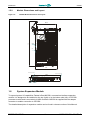
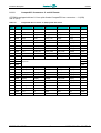
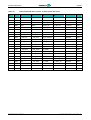
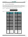
1
CPC508
3U CompactPCI
CPU Module
User Manual
Rev. 001 E
December 2012
The product described in this manual is compliant
with all related CE standards.
Product Title:
Document name:
Manual version:
Ref. docs:
CPC508
CPC508 User Manual
001 E
CPC508-UM-v1.02-R (IMES.467444.062 RE)
Copyright © 2012 Fastwel Co. Ltd. All rights reserved.
Revision Record
Rev. Index
Brief Description
Product Index
Date
001
Initial version
CPC508, MIC589
December 2012
Contact Information
Fastwel Co. Ltd
Fastwel Corporation US
Address:
108 Profsoyuznaya st.,
Moscow 117437,
Russian Federation
45 Main Street, Suite 319
Brooklyn, New York 11201
USA
Tel.:
+7 (495) 232-1681
+1 (718) 554-3686
Fax:
+7 (495) 232-1654
+1 (718) 797-0600
Toll free:
E-mail:
[email protected]
Web:
http://www.fastwel.com/
+1 (877) 787-8443 (1-877-RURUGGED)
CPC508
Table of Contents
Table of Contents ..............................................................................................................................................1
List of Tables .....................................................................................................................................................2
List of Figures ....................................................................................................................................................3
Notation Conventions.........................................................................................................................................4
General Safety Precautions................................................................................................................................5
Unpacking, Inspection and Handling...................................................................................................................6
Three Year Warranty..........................................................................................................................................7
1
Introduction...................................................................................................................................... 8
1.1
1.2
1.3
1.4
1.5
1.6
2
Functional Description ...................................................................................................................14
2.1
2.2
3
3.5
Safety Regulations ................................................................................................................................24
Installation Procedure............................................................................................................................25
Removal Procedure...............................................................................................................................25
Peripheral Devices Installation...............................................................................................................26
3.4.1
CompactFlash Cards Installation ...........................................................................................26
3.4.2
USB Devices Installation .......................................................................................................26
3.4.3
Battery Replacement.............................................................................................................26
Installation of MIC589 Mezzanine Expansion Module .............................................................................27
Configuration and Programming....................................................................................................28
4.1
4.2
5
Module Interfaces..................................................................................................................................14
2.1.1
CompactPCI Bus Connectors................................................................................................14
2.1.1.1
CompactPCI Connector Color Coding....................................................................14
2.1.1.2
CompactPCI Connectors J1 and J2 Pinouts...........................................................15
2.1.2
Connector for Mezzanine Module ..........................................................................................17
2.1.3
Keyboard/Mouse Interface ....................................................................................................18
2.1.4
USB Interfaces......................................................................................................................18
2.1.5
Graphics Controller ...............................................................................................................19
2.1.5.1
VGA Interface and Connector................................................................................19
2.1.5.2
LVDS Interface .....................................................................................................19
2.1.6
Serial Interfaces (RS232 and RS422/485)..............................................................................20
2.1.7
Gigabit Ethernet....................................................................................................................20
2.1.8
SATA Ports...........................................................................................................................21
2.1.9
HD Audio..............................................................................................................................21
2.1.10
CompactFlash Socket ...........................................................................................................21
2.1.11
LED Indicators L1 and L2......................................................................................................22
Data Storage Subsystem for CPC508 ....................................................................................................23
Installation.......................................................................................................................................24
3.1
3.2
3.3
3.4
4
Overview ................................................................................................................................................8
Technical Characteristics.........................................................................................................................8
CPC508 Versions..................................................................................................................................10
Delivery Checklist..................................................................................................................................11
CPC508 Diagrams ................................................................................................................................11
1.5.1
Block Diagram ......................................................................................................................12
1.5.2
Module Dimensions and Layout.............................................................................................13
System Expansion Module ....................................................................................................................13
WDT Operation .....................................................................................................................................28
L1 User LED Control .............................................................................................................................28
Phoenix® BIOS Setup .....................................................................................................................29
5.1
5.2
CP C5 0 8
Starting BIOS Setup..............................................................................................................................29
Main Menu............................................................................................................................................30
Us e r
M a n u a l
1
© 2 0 1 2
F a s t w e l
V e r . 0 0 1
E
CPC508
5.3
5.4
5.5
5.6
5.7
5.8
6
Additional Information ....................................................................................................................40
6.1
7
7.3
7.4
7.5
Introduction...........................................................................................................................................41
MIC589 Diagrams .................................................................................................................................41
7.2.1
MIC589 Block Diagram .........................................................................................................41
7.2.2
MIC589 Connectors Layout ...................................................................................................42
7.2.3
MIC589 Components Layout .................................................................................................43
Specifications........................................................................................................................................44
MIC589 Delivery Checklist.....................................................................................................................45
MIC589 Interfaces.................................................................................................................................45
7.5.1
MIC589 Interfaces List ..........................................................................................................45
7.5.1.1
Front Panel (4HP) Interfaces .................................................................................45
7.5.1.2
Interfaces Routed to CPCI J2 Connector ...............................................................45
Supplementary Information............................................................................................................46
8.1
9
System Power.......................................................................................................................................40
MIC589 Mezzanine Expansion Module...........................................................................................41
7.1
7.2
8
5.2.1
IDE Primary/Master...............................................................................................................31
5.2.2
SATA Port 1 – Port 3.............................................................................................................32
5.2.3
Memory Cache .....................................................................................................................32
5.2.4
Boot Features .......................................................................................................................33
Advanced Menu ....................................................................................................................................33
5.3.1
PnP Configuration Submenu .................................................................................................34
Intel Menu.............................................................................................................................................34
5.4.1
CPU Control Submenu..........................................................................................................35
5.4.2
Video (Intel IGD) Control Submenu........................................................................................35
5.4.3
ICH Control Submenu ...........................................................................................................36
5.4.3.1
PCI Express Control Submenu..............................................................................36
5.4.3.2
ICH USB Control Submenu ...................................................................................37
Security Menu.......................................................................................................................................37
Boot Menu ............................................................................................................................................38
Custom Menu .......................................................................................................................................38
5.7.1
MIC589 Peripheral ................................................................................................................39
Exit Menu .............................................................................................................................................39
Related Standards and Specifications....................................................................................................46
Useful Abbreviations, Acronyms and Short-cuts............................................................................47
List of Tables
Table 2-1:
Table 2-2:
Table 2-3:
Table 2-4:
Table 2-5:
Table 2-6:
Table 2-7:
Table 2-8:
Table 6-1:
Table 9-1:
Table 9-2:
CP C5 0 8
CompactPCI Connector Coding Colors .......................................................................................14
CompactPCI Bus Connector J1 (XS8) System Slot Pinout ...........................................................15
32-bit CompactPCI Bus Connector J2 (XS7) System Slot Pinout..................................................16
Pinout of XS6 Connector for MIC589 Mezzanine Module.............................................................17
USB1 and USB2 Pinouts (CPC508 Front Panel)..........................................................................18
VGA (XS1) Front Panel Connector Pinout ...................................................................................19
Gigabit Ethernet Connectors Pinouts...........................................................................................20
L1 and L2 LEDs Functions..........................................................................................................22
DC Input Voltage Ranges and Limits...........................................................................................40
Related Standards......................................................................................................................46
Related Specifications ................................................................................................................46
Us e r
M a n u a l
2
© 2 0 1 2
F a s t w e l
V e r . 0 0 1
E
CPC508
List of Figures
Figure 1-1:
Figure 1-2:
Figure 2-1:
Figure 2-2:
Figure 2-3:
Figure 2-4:
Figure 2-5:
Figure 2-6:
Figure 2-7:
Figure 5-1:
Figure 5-2:
Figure 5-3:
Figure 5-4:
Figure 5-5:
Figure 5-6:
Figure 5-7:
Figure 5-8:
Figure 5-9:
Figure 5-10:
Figure 5-11:
Figure 5-12:
Figure 5-13:
Figure 5-14:
Figure 5-15:
Figure 5-16:
Figure 5-17:
Figure 7-1:
Figure 7-2:
Figure 7-3:
CPC508 Block Diagram..............................................................................................................12
CPC508 Module Dimensions and Layout ....................................................................................13
CompactPCI Connectors J1 and J2 à ........................................................................................14
XS6 Expansion Connector for MIC589 Mezzanine Module...........................................................17
USB1 (XS2) and USB2 (XS3) Sockets ........................................................................................18
VGA (XS1) Front Panel Connector..............................................................................................19
Ethernet Connectors...................................................................................................................20
CompactFlash Socket.................................................................................................................21
Data Storage Subsystem ............................................................................................................23
POST Screen Image ..................................................................................................................29
Main Menu Screen .....................................................................................................................30
IDE Primary/Master Screen ........................................................................................................31
Memory Cache Screen ...............................................................................................................32
Boot Features ............................................................................................................................33
Advanced Menu Screen..............................................................................................................33
PnP Configuration Submenu Screen ...........................................................................................34
Intel Menu Screen ......................................................................................................................34
CPU Control Submenu Screen ...................................................................................................35
Video (Intel IGD) Control Submenu Screen .................................................................................35
ICH Control Sub-Menu Screen....................................................................................................36
PCI Express Control Submenu Screen........................................................................................36
ICH USB Control Submenu Screen .............................................................................................37
Security Menu Screen ................................................................................................................37
Boot Menu Screen......................................................................................................................38
Custom Menu Screen .................................................................................................................38
Exit Menu Screen .......................................................................................................................39
MIC589 Block Diagram...............................................................................................................41
MIC589 Connectors Layout ........................................................................................................42
MIC589 Components Layout and Dimensions (Top) ....................................................................43
All information in this document is provided for reference only, with no warranty of its suitability for any specific purpose. This information has been thoroughly checked and
is believed to be entirely reliable and consistent with the product that it describes. However, Fastwel accepts no responsibility for inaccuracies, omissions or their
consequences, as well as liability arising from the use or application of any product or example described in this document.
Fastwel Co. Ltd. reserves the right to change, modify, and improve this document or the products described in it, at Fastwel's discretion without further notice. Software
described in this document is provided on an “as is” basis without warranty. Fastwel assumes no liability for consequential or incidental damages originated by the use of
this software.
This document contains information, which is property of Fastwel Co. Ltd. It is not allowed to reproduce it or transmit by any means, to translate the document or to convert
it to any electronic form in full or in parts without antecedent written approval of Fastwel Co. Ltd. or one of its officially authorized agents.
Fastwel and Fastwel logo are trademarks owned by Fastwel Co. Ltd., Moscow, Russian Federation. CompactPCI is a trademark of the PCI industrial Computers
Manufacturers Group. Ethernet is a registered trademark of Xerox Corporation. IEEE is a registered trademark of the Institute of Electrical and Electronics Engineers Inc.
Intel is a trademark of Intel Corporation. Pentium M and Celeron M are trademarks of Intel Corporation. Microsoft is a trademark of the Microsoft corporation. In addition,
this document may include names, company logos and trademarks, which are registered trademarks and, therefore, are property of their respective owners.
Fastwel welcomes suggestions, remarks and proposals regarding the form and the content of this Manual.
CP C5 0 8
Us e r
M a n u a l
3
© 2 0 1 2
F a s t w e l
V e r . 0 0 1
E
CPC508
Notation Conventions
Warning, ESD Sensitive Device!
This symbol draws your attention to the information related to electro static sensitivity of your
product and its components. To keep product safety and operability it is necessary to handle
it with care and follow the ESD safety directions.
Warning!
This sign marks warnings about hot surfaces. The surface of the heatsink and some
components can get very hot during operation. Take due care when handling, avoid
touching hot surfaces!
Caution: Electric Shock!
This symbol warns about danger of electrical shock (> 60 V) when touching products or
parts of them. Failure to observe the indicated precautions and directions may expose your
life to danger and may lead to damage to your product.
Warning!
Information marked by this symbol is essential for human and equipment safety.
Read this information attentively, be watchful.
Note...
This symbol and title marks important information to be read attentively for your own benefit.
CP C5 0 8
Us e r
M a n u a l
4
© 2 0 1 2
F a s t w e l
V e r . 0 0 1
E
CPC508
General Safety Precautions
This product was developed for fault-free operation. Its design provides conformance to all related
safety requirements. However, the life of this product can be seriously shortened by improper
handling and incorrect operation. That is why it is necessary to follow general safety and
operational instructions below.
Warning!
All operations on this device must be carried out by sufficiently
skilled personnel only.
Warning!
When handling this product, special care must be taken not to hit
the heatsink (if installed) against another rigid object. Also, be
careful not to drop the product, since this may cause damage
to the heatsink, CPU or other sensitive components as well.
Please, keep in mind that any physical damage to this product
is not covered under warranty.
Note:
This product is guaranteed to operate within the published
temperature ranges and relevant conditions. However, prolonged
operation near the maximum temperature is not recommended by
Fastwel or by electronic chip manufacturers due to thermal stress
related failure mechanisms. These mechanisms are common to all
silicon devices, they can reduce the MTBF of the product by
increasing the failure probability. Prolonged operation at the lower
limits of the temperature ranges has no limitations.
Caution, Electric Shock!
Before installing this product into a system and before installing
other devices on it, always ensure that your mains power is switched
off.
Always disconnect external power supply cables during all handling
and maintenance operations with this module to avoid serious
danger of electrical shock.
CP C5 0 8
Us e r
M a n u a l
5
© 2 0 1 2
F a s t w e l
V e r . 0 0 1
E
CPC508
Unpacking, Inspection and Handling
Please read the manual carefully before unpacking the module or mounting the device into your
system. Keep in mind the following:
ESD Sensitive Device!
Electronic modules and their components are sensitive to static
electricity. Even a non-perceptible by human being static discharge
can be sufficient to destroy or degrade a component's operation!
Therefore, all handling operations and inspections of this product
must be performed with due care, in order to keep product integrity
and operability:
n
Preferably, unpack or pack this product only at EOS/ESD safe workplaces. Otherwise, it is
important to be electrically discharged before touching the product. This can be done by
touching a metal part of your system case with your hand or tool. It is particularly important
to observe anti-static precautions when setting jumpers or replacing components.
n
If the product contains batteries for RTC or memory back-up, ensure that the module is not
placed on conductive surfaces, including anti-static mats or sponges. This can cause shortcircuit and result in damage to the battery and other components.
Store this product in its protective packaging while it is not used for operational purposes.
n
Unpacking
The product is carefully packed in an antistatic bag and in a carton box to protect it against
possible damage and harmful influence during shipping. Unpack the product indoors only at a
temperature not less than +15°C and relative humidity not more than 70%. Please note, that if the
product was exposed to the temperatures below 0°С for a long time, it is necessary to keep it at
normal conditions for at least 24 hours before unpacking. Do not keep the product close to a heat
source.
Following ESD precautions, carefully take the product out of the shipping carton box. Proper
handling of the product is critical to ensure correct operation and long-term reliability. When
unpacking the product, and whenever handling it thereafter, be sure to hold the module preferably
by the front panel, card edges or ejector handles. Avoid touching the components and connectors.
Retain all original packaging at least until the warranty period is over. You may need it for
shipments or for storage of the product.
Initial Inspection
Although the product is carefully packaged, it is still possible that shipping damages may occur.
Careful inspection of the shipping carton can reveal evidence of damage or rough handling. Should
you notice that the package is damaged, please notify the shipping service and the manufacturer
as soon as possible. Retain the damaged packing material for inspection.
After unpacking the product, you should inspect it for visible damage that could have occurred
during shipping or unpacking. If damage is observed (usually in the form of bent component leads
or loose socketed components), contact Fastwel's official distributor from which you have
purchased the product for additional instructions. Depending on the severity of the damage, the
product may even need to be returned to the factory for repair. DO NOT apply power to the product
if it has visible damage. Doing so may cause further, possibly irreparable damage, as well as result
in a fire or electric shock hazard.
If the product contains socketed components, they should be inspected to make sure they are
seated fully in their sockets.
CP C5 0 8
Us e r
M a n u a l
6
© 2 0 1 2
F a s t w e l
V e r . 0 0 1
E
CPC508
Handling
In performing all necessary installation and application operations, please follow only the
instructions supplied by the present manual.
In order to keep Fastwel’s warranty, you must not change or modify this product in any way, other
than specifically approved by Fastwel or described in this manual.
Technical characteristics of the systems in which this product is installed, such as operating
temperature ranges and power supply parameters, should conform to the requirements stated by
this document.
Retain all the original packaging, you will need it to pack the product for shipping in warranty cases
or for safe storage. Please, pack the product for transportation in the way it was packed by the
supplier.
When handling the product, please, remember that the module, its components and connectors
require delicate care. Always keep in mind the ESD sensitivity of the product.
Three Year Warranty
Fastwel Co. Ltd. (Fastwel), warrants that its standard hardware products will be free from defects
in materials and workmanship under normal use and service for the currently established warranty
period. Fastwel’s only responsibility under this warranty is, at its option, to replace or repair any
defective component part of such products free of charge.
Fastwel neither assumes nor authorizes any other liability in connection with the sale, installation
or use of its products. Fastwel shall have no liability for direct or consequential damages of any
kind arising out of sale, delay in delivery, installation, or use of its products.
If a product should fail through Fastwel's fault during the warranty period, it will be repaired free of
charge. For out of warranty repairs, the customer will be invoiced for repair charges at current
standard labor and materials rates.
Warranty period for Fastwel products is 36 months since the date of purchase.
The warranty set forth above does not extend to and shall not apply to:
1.
Products, including software, which have been repaired or altered by other than
Fastwel personnel, unless Buyer has properly altered or repaired the products in
accordance with procedures previously approved in writing by Fastwel.
2.
Products, which have been subject to power, supply reversal, misuse, neglect,
accident, or improper installation.
Returning a product for repair
1.
Apply to Fastwel company or to any of the Fastwel's official representatives for the
Product Return Authorization.
2.
Attach a failure inspection report with a product to be returned in the form, accepted by
customer, with a description of the failure circumstances and symptoms.
3.
Carefully package the product in the antistatic bag, in which the product had been
supplied. Failure to package in antistatic material will VOID all warranties. Then
package the product in a safe container for shipping.
4.
The customer pays for shipping the product to Fastwel or to an official Fastwel
representative or dealer.
CP C5 0 8
Us e r
M a n u a l
7
© 2 0 1 2
F a s t w e l
V e r . 0 0 1
E
Introduction
CPC508
1
Introduction
1.1
Overview
The product described in this Manual is CPC508 – a 3U CompactPCI PlusIO (PICMG 2.30)
CPU module.
For high-speed data exchange CPC508 employs 32-bit PCI bus together with two Gigabit
Ethernet channels, four x1 PCI Express lanes, DVI and eight USB 2.0 channels .
Modular design allows flexible system configuration, thus providing optimum price to
performance ratio. To expand the functionality of CPC508, the MIC589 mezzanine
interface expansion module is used.
The operational stability of CPC508 make it perfect for use in industrial applications.
1.2
Technical Characteristics
n
n
n
n
n
CP C5 0 8
Intel® processors:
Low power Atom core, integrated memory and graphics controllers
§
Intel Pineview-M, single core (N450, for CPC508-01)
§
Intel Pineview-D, dual core (D510, for CPC508-03)
§
IA 32-bit & 64-bit technology;
§
Intel SIMD2 & 3 (SSE2 + SSE3 + SSSE3);
§
Hyperthreading Technology (2 threads);
§
Level 1 cache memory (32 KB instructions, 24 KB data);
§
Level 2 cache memory: 512 KB (N450), 1 MB (D510);
§
Intel SpeedStep Technology
Intel chipset: ICH8M
System memory:
§
DDR2 SDRAM 667 MHz w/o ECC
§
1 GB, soldered, 64-bit addressing
Integrated high performance graphics controller:
§
VGA front panel connector, CRT displays support with resolutions of up to
1400x1050 60 Hz for N450 and up to 2048×1536 60 Hz for D510;
§
LVDS interface (resolutions up to 1280x800 60 Hz for N450 and 1366x768 60 Hz for
D510, single channel, 18-bit), routed to mezzanine connector, available via MIC589
module
PCI bus:
§
Routed to CPCI J1 connector
§
Spec. v.2.3 support
§
32-bit / 33 MHz
§
Support for up to 7 bus master devices
Us e r
M a n u a l
8
© 2 0 1 2
F a s t w e l
V e r . 0 0 1
E
Introduction
n
n
n
n
n
n
n
n
n
n
n
n
n
n
CP C5 0 8
CPC508
LPC bus:
§
Routed to mezzanine connector
§
Spec. v1.0 compatibility
§
Support for two Master/DMA devices
PCI Express: four x1 lanes
§
Routed to CPCI J2 connector
§
Spec 1.1 compatibility
§
Support for up to four x1 devices (up to 2.5 Gbit/s)
Flash BIOS:
§
SPI interface, 16 Mbit
§
In-system modification
NAND flash disk:
§
4 GB NAND flash, dual channel, soldered
§
SATA interface (50 MB/s read, 45 MB/s write)
§
Can be used as boot device
CompactFlash Type II socket:
§
Support for PIO & UDMA modes
§
UltraATA 100/66/33
SATA interface:
§
Up to 300 MB/s
§
Two ports
§
Routed to CPCI J2 connector
Gigabit Ethernet interfaces:
§
Two PCI-E controllers
§
10/100/1000 Mbps
§
Two RJ-45 frontpanel connectors
§
Front/rear switchable
USB:
§
1.1 and 2.0 support,
§
Up to 8 devices: two at CPC508 front panel, two via MIC589 (mezzanine connector),
four via CPCI J2 available at the backplane
FRAM:
§
Available via SMBus
§
64 Kbit, 256 B RAM for BIOS Setup parameters storage
Real-time clock
§
Integrated in ICH8M
§
CR2032 battery backup (3V)
Audio
§
Discrete HD audio
§
Routed to mezzanine connector
Watchdog timer:
§
Fixed timeout period (1.6 s)
§
Reset source
Hardware monitor
§
Available via SMBus
§
Power voltages monitoring
§
CPU and PCB temperatures monitoring
Front panel LED indicators
§
Disk drives activity LED
§
Programmable user LED
Us e r
M a n u a l
9
© 2 0 1 2
F a s t w e l
V e r . 0 0 1
E
Introduction
n
CPC508
Mezzanine connector:
§
Used for connection of MIC589 interface expansion module
§
HD Audio, two USB ports, LVDS, 8-bit local bus
Weight: 0.450 kg max
Dimensions: 130.5 mm × 213.0 mm х 20.32 mm
Power voltage: +5 V ± 5% from CPCI connector
Consumption current:
§
CPC508-01: 2.8 A
§
CPC508-03: 3.1 A
MTBF: 140000 hours
OS compatibility:
§
FreeDOS
§
Windows XP (Embedded)
§
Linux 2.6
§
QNX 6.5
n
n
n
n
n
n
1.3
CPC508 Versions
CPC508 is available in two versions:
1
–
1
2
–
3
\
4
Basic product name:
CPC508
2
3
Version:
Version
CPU
01
Intel Pineview-M (N450)
03
Intel Pineview-D (D510)
Operating temperature range:
I
4
Industrial, -40°C … +85°C
Other options:
Coating
\COATED
Protective coating
Operating System
\XPE
\LNX
CP C5 0 8
Us e r
M a n u a l
Windows XP Embedded
Linux 2.6
10
© 2 0 1 2
F a s t w e l
V e r . 0 0 1
E
Introduction
1.4
CPC508
Delivery Checklist
The CPC508 delivery set includes:
1.
2.
3.
4.
CPC508 processor module
MIC 23008 CompactFlash memory module with preinstalled Windows XPe
(only if \XPE option is selected)
Antistatic bag
Consumer carton box (~ 230×155×45 mm, gross weight 0.650 kg max)
Note:
Keep the antistatic bag and the original package at least until
the warranty period is over. It can be used for future storage or
warranty shipments.
1.5
CPC508 Diagrams
The diagrams in this section give visual information about the CPC508 module design, connectors
and components layout. The diagrams may not reflect insignificant differences between the
CPC508 versions.
6
CP C5 0 8
Us e r
M a n u a l
11
© 2 0 1 2
F a s t w e l
V e r . 0 0 1
E
Introduction
1.5.1
CPC508
Block Diagram
Figure 1-1:
CPC508 Block Diagram
Soldered
NAND Flash
4 GB
Soldered
DDR2 SDRAM
1 GB
XS1
SATA NAND
Flash
Controller
PineView-M
VGA
CRT
Gigabit
Ethernet
i82574
XS4
XS2
XS3
Gigabit
LAN 1, 2
Gigabit
Ethernet
Multiplexor
USB 1
Gigabit
Ethernet
i82574
IDE
Compact
Flash
SATA
SATA
Ports 1-2
x4 DMI
XP5
Gigabit
LAN 1
Gigabit
LAN 2
PCIE
PCIE
PCIE
USB 2
XS7(J2)
PCI-E 1-4
ICH8-M
USB 5-8
PCI
PCI-PCI
Bridge
SMBus
32-bit
PCI Bus
Hardware
Monitor
LM87
FRAM
CK-505
& SS
Clocking
XS8 (J1)
SPI BIOS
16 Mbit
LPC Bus
FPGA
Supervisor
WDT
CPU Core VR
Chipset VR
Memory VR
Power Supply
HD Link
USB 3-4
8-bit Local
Bus
LVDS
XS6
CP C5 0 8
Us e r
M a n u a l
12
© 2 0 1 2
F a s t w e l
V e r . 0 0 1
E
Introduction
1.5.2
CPC508
Module Dimensions and Layout
Figure 1-2:
CPC508 Module Dimensions and Layout
88.89
1
1
XS5
XS6
212.5
CPC508
Reset
XP3
1
XP4
2
1
CF
1
(J1)
100
(J2)
Lower Fixing Screw
Upper Fixing Screw
130.5
Eth1
20.32
Eth2
Handle
1.6
L2 USB2 USB1
L1
SVGA
Lock Button
System Expansion Module
To expand system I/O capabilities Fastwel offers MIC589, a mezzanine interface expansion
module. It is designed to be installed on the top (right) or on the bottom side (left) of CPC508
processor module and is connected via XS6 connector. MIC589 is supplied with the adaptor
connector to enable connection to CPC508.
The detailed description of expansion module can be found in relevant section of this Manual.
CP C5 0 8
Us e r
M a n u a l
13
© 2 0 1 2
F a s t w e l
V e r . 0 0 1
E
Functional Description
CPC508
2
Functional Description
2.1
Module Interfaces
22
2.1.1
CompactPCI Bus Connectors
Figure 2-1:
CompactPCI Connectors J1 and J2 à
J2
The CPC508 is designed for a CompactPCI bus architecture,
but it utilizes only two of standard CompactPCI connectors –
J1 and J2. The CompactPCI standard is electrically identical
to the PCI local bus. However, these systems are improved to
support multiple slots and to operate in harsh industrial
environments.
1
25
J1 stadard CompactPCI connector is marked as XS8 on
board, J2 (CompactPCI 2.30) is marked as XS7.
2.1.1.1
J1
CompactPCI Connector Color Coding
Guide lugs on CompactPCI connectors serve to ensure a
correct mating of connectors. A proper mating is guaranteed
also by the use of color coded keys for 3.3V and 5V
operation. Color coded keys prevent accidental installation of
a 5V module into a 3.3V slot. CompactPCI backplane
connectors' keying depends always on the signaling (VIO)
level. On universal backplanes supporting both sinalling
levels, VIO level is selected by a jumper on the backplane.
Note:
Pinrows
F and Z
are
GND pins
1
F
E DC BA
Z
CPC508 is a universal module with 3.3V or 5V signalling
voltage level.
Coding key colors are described below:
Table 2-1:
CompactPCI Connector Coding Colors
Voltage Level
Key Color
3.3 V
Cadmium Yellow
5V
Brilliant Blue
Universal module (5V and 3.3V)
None
CompactPCI connector pinouts appear on the following pages.
CP C5 0 8
Us e r
M a n u a l
14
© 2 0 1 2
F a s t w e l
V e r . 0 0 1
E
Functional Description
2.1.1.2
CPC508
CompactPCI Connectors J1 and J2 Pinouts
CPC508 is equipped with two 2´2 mm pitch female CompactPCI bus connectors – J1 (XS8)
and J2 (XS7).
Table 2-2:
CompactPCI Bus Connector J1 (XS8) System Slot Pinout
Pin
Z
A
B
C
D
E
F
25
GND
5V
REQ64#
ENUM#
3.3V
5V
GND
24
GND
AD[1]
5V
LNG_VIO
AD[0]
ACK64#
GND
23
GND
3.3V
AD[4]
AD[3]
LNG_5V
AD[2]
GND
22
GND
AD[7]
GND
LNG_3.3V
AD[6]
AD[5]
GND
21
GND
3.3V
AD[9]
AD[8]
M66EN
C/BE[0]#
GND
20
GND
AD[12]
GND
VIO
AD[11]
AD[10]
GND
19
GND
3.3V
AD[15]
AD[14]
LNG_GND
AD[13]
GND
18
GND
SERR#
GND
3.3V
PAR
C/BE[1]#
GND
17
GND
3.3V
IPMB_SCL
IPMB_SDA
LNG_GND
PERR#
GND
16
GND
DEVSEL#
GND
VIO
STOP#
LOCK#
GND
15
GND
3.3V
FRAME#
IRDY#
SHRT_GND
TRDY#
GND
14
GND
13
GND
12
GND
11
GND
AD[18]
AD[17]
AD[16]
LNG_GND
C/BE[2]#
GND
10
GND
AD[21]
GND
3.3V
AD[20]
AD[19]
GND
9
GND
C/BE[3]#
SHRT_GND
AD[23]
LNG_GND
AD[22]
GND
8
GND
AD[26]
GND
VIO
AD[25]
AD[24]
GND
7
GND
AD[30]
AD[29]
AD[28]
LNG_GND
AD[27]
GND
6
GND
REQ0#
GND
LNG_3.3V
CLK0
AD[31]
GND
5
GND
BRSVP1A5
BRSVP1B5
RST#
LNG_GND
GNT0#
GND
4
GND
IPMB_PWR
HEALTHY#
LNG_VIO
INTP
INTS
GND
3
GND
INTA#
INTB#
INTC#
LNG_5V
INTD#
GND
2
GND
TCK
5V
TMS
TDO
TDI
GND
1
GND
5V
-12V
TRST#
+12V
5V
GND
CP C5 0 8
Us e r
GND
Key Area
GND
GND
M a n u a l
15
© 2 0 1 2
F a s t w e l
V e r . 0 0 1
E
Functional Description
Table 2-3:
CPC508
32-bit CompactPCI Bus Connector J2 (XS7) System Slot Pinout
Pin
Z
A
B
C
D
E
F
22
GND
GA4
GA3
GA2
GA1
GA0
GND
21
GND
CLK6
GND
2_ETH_B+
1_ETH_D+
1_ETH_B+
GND
20
GND
CLK5
GND
2_ETH_B-
1_ETH_D-
1_ETH_B-
GND
19
GND
GND
GND
2_ETH_A+
1_ETH_C+
1_ETH_A+
GND
18
GND
2_ETH_D+
2_ETH_C+
2_ETH_A-
1_ETH_C-
1_ETH_A-
GND
17
GND
2_ETH_D-
2_ETH_C-
PRST#
REQ6#
GNT6#
GND
16
GND
4_PE_CLK-
2_PE_CLK+
DEG#
GND
Reserved
GND
15
GND
4_PE_CLK+
2_PE_CLK-
FAL#
REQ5#
GNT5#
GND
14
GND
3_PE_CLK-
1_PE_CLK+
4_PE_CLKE#
–
Reserved
GND
13
GND
3_PE_CLK+
1_PE_CLK-
3_PE_CLKE#
–
–
GND
12
GND
4_PE_Rx00+
1_PE_CLKE#
2_PE_CLKE#
–
–
GND
11
GND
4_PE_Rx00-
4_PE_Tx00+
4_USB2+
–
–
GND
10
GND
3_PE_Rx00+
4_PE_Tx00-
4_USB2-
–
–
GND
9
GND
3_PE_Rx00-
3_PE_Tx00+
3_USB2+
–
–
GND
8
GND
2_PE_Rx00+
3_PE_Tx00-
3_USB2-
–
2_SATA_Rx+
GND
7
GND
2_PE_Rx00-
2_PE_Tx00+
2_USB2+
2_SATA_Tx+
2_SATA_Rx-
GND
6
GND
1_PE_Rx00+
2_PE_Tx00-
2_USB2-
2_SATA_Tx-
1_SATA_Rx+
GND
5
GND
1_PE_Rx00-
1_PE_Tx00+
1_USB2+
1_SATA_Tx+
1_SATA_Rx-
GND
4
GND
VIO
1_PE_Tx00-
1_USB2-
1_SATA_Tx-
Reserved
GND
3
GND
CLK4
GND
GNT3#
REQ4#
GNT4#
GND
2
GND
CLK2
CLK3
SYSEN#
GNT2#
REQ3#
GND
1
GND
CLK1
GND
REQ1#
GNT1#
REQ2#
GND
CP C5 0 8
Us e r
M a n u a l
16
© 2 0 1 2
F a s t w e l
V e r . 0 0 1
E
Functional Description
2.1.2
CPC508
Connector for Mezzanine Module
MIC589 mezzanine module is used to enhance I/O capabilities of CPC508. It is installed on the top
side (to the right) of CPC508 processor module or on the bottom side (to the left) using adapter
connector. 72-contact XS6 high speed through connector socket is used for connection of MIC589.
See description of MIC589 expansion module in the relevant section of this document.
Figure 2-2:
XS6 Expansion Connector for MIC589 Mezzanine Module
2
1
Table 2-4:
CP C5 0 8
Us e r
Pinout of XS6 Connector for MIC589 Mezzanine Module
Contact
Signal
Contact
Signal
1
3
5
7
9
11
13
15
17
19
21
23
25
27
29
31
33
35
37
39
41
43
45
47
49
51
53
55
57
59
61
63
65
67
69
71
GND
LED1
USB_4_5_OC#
USB4+
USB4+5V
LED2
AD3.3V(1)
AD3.3V(3)
AD3.3V(5)
AD3.3V(7)
ALE
IOW#
SW_COM3
SW_CAN_1
CSA1#
CSA2#
CAN_CS1#
GND
INT1
INT3
INT5
+5V
COM3_ON
COM3_TE
GND
SMBCLK
INT4
INT6
COM4_ON
COM4_TE
GND
GND
AC_SYNC
AC_SDOUT
GND
2
4
6
8
10
12
14
16
18
20
22
24
26
28
30
32
34
36
38
40
42
44
46
48
50
52
54
56
58
60
62
64
66
68
70
72
GND
USB5USB5+
AD3.3V(0)
CAN1_RESET#
+5V
CAN2_RESET#
AD3.3V(2)
AD3.3V(4)
AD3.3V(6)
DIR
IOR#
RESET#
SW_COM4
SW_CAN2
CSB1#
CSB2#
CAN_CS2#
GND
INT2
LVDS_A(0)#
LVDS_A(0)
+5V
LVDS_A(1)#
LVDS_A(1)
GND
SMBDAT
LVDS_A(2)
LVDS_A(2)#
LVDS_A_CK#
LVDS_A_CK
GND
AC_BITCLK
AC_SDIN0
AC_RST#
GND
M a n u a l
17
© 2 0 1 2
F a s t w e l
V e r . 0 0 1
E
Functional Description
2.1.3
CPC508
Keyboard/Mouse Interface
A keyboard and a mouse can be connected to CPC508 using front panel USB sockets.
CPC508 includes 8042-compatible keyboard controller emulator realized on FPGA.
2.1.4
USB Interfaces
The CPC508 supports eight USB 2.0 ports. Two ports (USB1 and USB2) are available on CPC508
front panel via two Type A connectors (XS2 and XS3). Two ports (USB3 and USB4) are routed to
XS6 connector and are available at MIC589 mezzanine module. Four USB ports (USB5...USB8)
are routed to J2 CompactPCI connector (PICMG 2.30) of CPC508.
Figure 2-3:
1
USB1 (XS2) and USB2 (XS3) Sockets
2
3
All ports support high-speed, full-speed, and low-speed operation.
Hi-speed USB 2.0 supports data transfer rate of up to 480 Mb/s.
One USB device may be connected to each port. To connect more
than eight USB devices use an external hub.
4
The USB power supply is protected by a self-resettable 500 mA
fuse.
Table 2-5:
USB1 and USB2 Pinouts (CPC508 Front Panel)
Pin Number
Signal
Function
In/Out
1
VCC
VCC signal
–
2
UV0-
Differential USB-
–
3
UV0+
Differential USB+
–
4
GND
GND signal
–
CP C5 0 8
Us e r
M a n u a l
18
© 2 0 1 2
F a s t w e l
V e r . 0 0 1
E
Functional Description
2.1.5
CPC508
Graphics Controller
A highly integrated 2D/3D graphics accelerator is included in the CPU. The internal graphics
controller provides interfaces to a standard analog monitor (VGA connector on CPC508 front
panel) or/and to digital displays. Dual monitor clone/extended desktop configurations are
supported.
2.1.5.1
VGA Interface and Connector
Figure 2-4:
VGA (XS1) Front Panel Connector
6
1
11
The 15-pin female D-Sub connector (XS1) on CPC508 front panel
is used to connect a CRT monitor to the CPC508 module.
Resolutions: CPC508-01 – up to 1400×1050, 60 Hz
CPC508-03 – up to 2048×1536, 60 Hz
5
10
Table 2-6:
15
Its pinout is in the table below.
VGA (XS1) Front Panel Connector Pinout
Pin Number
Signal
Function
In/Out
1
Red
Red video signal output
Out
2
Green
Green video signal output
Out
3
Blue
Blue video signal output
Out
12
DDCdata
I2C™ data
In/Out
13
Hsync
Horizontal sync.
TTL out
14
Vsync
Vertical sync.
TTL out
2
15
DDCclk
I C™ clock
Out
5, 6, 7, 8, 10
GND
Signal ground
–
4, 11, 9
NC
–
–
2.1.5.2
LVDS Interface
LVDS is routed to XS6 mezzanine connector to be available at MIC589 expansion module.
Single channel LVDS mode is supported, up to 18 bit/pixel, 25-112 MHz.
LCD panels (LVDS 18-bit) are supported with following resolutions:
CPC508-01 – 1280×800, 60 Hz,
CPC508-03 – 1366×768, 60 Hz.
CP C5 0 8
Us e r
M a n u a l
19
© 2 0 1 2
F a s t w e l
V e r . 0 0 1
E
Functional Description
2.1.6
CPC508
Serial Interfaces (RS232 and RS422/485)
Serial interfaces are available only if MIC589 interface expansion module is installed. There are
four serial ports available via MIC589 connectors and on backplane via CPCI J2 connector of
MIC589. See details in the relevant section of this document.
2.1.7
Gigabit Ethernet
The CPC508 board includes two 10Base-T/100Base-TX/1000Base-T Ethernet ports based on
Intel® 82574L Gigabit Ethernet PCI-E bus controllers. The Intel® 82574L Gigabit Ethernet
controller architecture combines high performance and low power consumption. The controller's
features include independent transmit and receive queues to limit PCI-E bus traffic, and a PCI-E
interface providing efficient bus utilization by increased use of bursts.
Figure 2-5:
Act
Ethernet Connectors
Link
Two RJ45 Gigabit Ethernet connectors are located on CPC508
front panel (XS4).
The interfaces provide auto-detection and switching between
10Base-T, 100Base-TX and 1000Base-T operation modes.
1
1
Each of the two Ethernet channels are software switchable to XS7 (CPCI J2, PICMG 2.30) to
provide system flexibility.
Table 2-7:
Gigabit Ethernet Connectors Pinouts
10Base-T
Pin
100Base-TX
1000Base-T
I/O
Signal
I/O
Signal
I/O
Signal
1
O
TX+
O
TX+
I/O
BI_DA+
2
O
TX–
O
TX–
I/O
BI_DA–
3
I
RX+
I
RX+
I/O
BI_DB+
4
–
–
–
–
I/O
BI_DC+
5
–
–
–
–
I/O
BI_DC–
6
I
RX–
I
RX–
I/O
BI_DB–
7
–
–
–
–
I/O
BI_DD+
8
–
–
–
–
I/O
BI_DD–
MDI / Standard Ethernet Cable
Integrated Ethernet LEDs
Line (green): This LED indicates network connection. The LED lights up when the line is
connected.
Act (green): This LED monitors network activity. The LED lights up when network packets are sent
or received through the RJ45 port. When this LED is not lit, it means that the computer is not
sending or receiving network data.
CP C5 0 8
Us e r
M a n u a l
20
© 2 0 1 2
F a s t w e l
V e r . 0 0 1
E
Functional Description
2.1.8
CPC508
SATA Ports
Two SATA ports are routed to CPCI J2 connector (PICMG 2.30).
2.1.9
HD Audio
CPC508 provides digital High Definition Audio interface routed via XS6 mezzanine connector to
MIC589 module and firther to the backplane via CPCI J2 connector of MIC589. The interface
includes line input/output and microphone input channels.
2.1.10
CompactFlash Socket
Figure 2-6:
CompactFlash Socket
To enable usage of CF memory cards CPC508 has a
CompactFlash Type I/II socket located on the top side of
the board. CF removable mass storage devices are fully
compatible with 16-bit ATA/ATAPI-4 IDE interface with
DMA support (CF Specification v.4.1).
CompactFlash socket is connected to the IDE port at the current version of CPC508. There is a bracket for
fixing a CF card in the socket.
Table 2-1:
CompactFlash Socket Pinout
Pin Number
Signal
Function
In/Out
1
2
3
4
5
6
7
8
9
10
11
12
13
14
15
16
17
18
19
20
21
22
23
24
25
26
27
28
29
30
31
32
33
34
35
36
GND
D03
D04
D05
D06
D07
IDE_CS0
GND
GND
GND
GND
GND
3.3 V
A06
A05
A04
A03
A02
A01
A00
D00
D01
D02
IOCS16
CD2
CD1
D11
D12
D13
D14
D15
IDE_CS1
VS1
IORD
IOWR
3.3 V WE
Ground signal
Data 3
Data 4
Data 5
Data 6
Data 7
Chip select 0
–
–
–
–
–
3.3 V power
–
–
–
–
Address 2
Address 1
Address 0
Data 0
Data 1
Data 2
–
–
–
Data 11
Data 12
Data 13
Data 14
Data 15
Chip select 1
–
I/O read
I/O write
3.3 V power
–
In/Out
In/Out
In/Out
In/Out
In/Out
Out
–
–
–
–
–
–
–
–
–
–
Out
Out
Out
In/Out
In/Out
In/Out
–
–
–
In/Out
In/Out
In/Out
In/Out
In/Out
Out
–
Out
Out
–
CP C5 0 8
Us e r
M a n u a l
21
© 2 0 1 2
F a s t w e l
V e r . 0 0 1
E
Functional Description
CPC508
Pin Number
Signal
Function
In/Out
37
38
39
40
41
42
43
44
45
46
47
48
49
50
INTRQ
3.3 V
CSEL
VS2
Reset
IORDY
INPACK
REG
ACTIVE
PDIAG
D08
D09
D10
GND
Interrupt
3.3 V power
Master/Slave
–
Reset
I/O ready
DMA Request
DMA Acknowledge
IDE Activity
DMA Mode Detect
Data 08
Data 09
Data 10
–
In
–
Out
–
Out
In
Out
–
–
–
In/Out
In/Out
In/Out
–
2.1.11
LED Indicators L1 and L2
There are two LED indicators at the front panel L1 and L2 described in the tablebelow.
Table 2-8:
L1 and L2 LEDs Functions
Function
Name
L1
Power indicator/
user LED
Color
Description
Green
After switching power on lights green. Also can
be controlled via LED1_EN bit as user LED.
Can be controlled via LED2_EN bit as user
LED.
Red
L2
CP C5 0 8
Drives activity indicator
Us e r
M a n u a l
Green
SATA, NAND and Flash drives activity.
22
© 2 0 1 2
F a s t w e l
V e r . 0 0 1
E
Functional Description
2.2
CPC508
Data Storage Subsystem for CPC508
According to PICMG 2.30 specification, CPC508 supports data storage devices installed in Serial
backplane slots. Slot names (1_SATA – 4_SATA) are shown in the figure below.
Figure 2-7:
Data Storage Subsystem
CPC508 supports two SATA channels. These drives are installed in slots 1 and 2 (5-J1 и 6-J1).
SATA drives operation in slots 7-J1 and 8-J1 is not supported. Fastwel KIC550 or other modules
can be used as carrier boards.
CP C5 0 8
Us e r
M a n u a l
23
© 2 0 1 2
F a s t w e l
V e r . 0 0 1
E
Installation
3
CPC508
Installation
The CPC508 is easy to install. However, it is necessary to follow the procedures and safety
regulations below to install the module correctly without damage to the hardware, or harm to
personnel.
The installation of the peripheral drivers is described in the accompanying information files. For
details on installation of an operating system, please refer to the relevant software documentation.
3.1
Safety Regulations
The following safety regulations must be observed when installing or operating the CPC508.
Fastwel assumes no responsibility for any damage resulting from infringement of these rules.
Warning!
When handling or operating the module, special attention should be
paid to the heatsink, because it can get very hot during operation.
Do not touch the heatsink when installing or removing the module.
Moreover, the module should not be placed on any surface or in any
kind of package until the module and its heatsink have cooled down
to ambient temperature.
Caution!
If your module does not allow hotswapping, switch off the system
power before installing the module in a free slot. Disregarding this
requirement could be harmful for your life or health and can damage
the module or entire system.
ESD Sensitive Equipment!
This product comprises electrostatically sensitive components.
Please follow the ESD safety instructions to ensure module's
operability and reliability:
n
n
Use grounding equipment, if working at an anti-static
workbench. Otherwise, discharge yourself and the tools
in use before touching the sensitive equipment.
Try to avoid touching contacts, leads and components.
Extra caution should be taken in cold and dry weather.
CP C5 0 8
Us e r
M a n u a l
24
© 2 0 1 2
F a s t w e l
V e r . 0 0 1
E
Installation
CPC508
3.2
Installation Procedure
To install CPC508 in a system, follow the instructions below.
1.
Keep to the safety regulations of the Section 3.1 when performing the following
operations.
Warning!
Failure to accomplish the following instruction may damage the
module or result in incorrect system operation.
2.
Ensure that the module configuration corresponds to the application requirements before
installing. For information regarding the configuration of the CPC508, refer to Chapter 4.
For the installation of CPC508 specific peripheral devices and I/O devices refer to the
appropriate sections in Chapter 3. For details on installation of expansion modules, refer
to respective sections of this document.
3.
If the module is intended for operation with a mezzanine module, install the mezzanine
module following corresponding instructions.
4.
To install the CPC508:
1.
Make sure that no power is connected to the system.
2.
Avoiding contact with other modules of the system, carefully insert the module into
the chosen slot until it contacts the backplane connectors. Do not apply force
pushing the module into the backplane connectors.
3.
Using the front panel ejector handle (handles), engage the module with the
backplane. The module is completely engaged, when the ejector handle is locked.
If the mezzanine module is installed, ensure simultaneous locking of both handles.
4.
Fix the module with the front panel retaining screws.
5.
Connect the required external interfacing cables to the module's connectors and
make sure that the module and all connected cables are properly fixed.
The CPC508 is now ready for operation. Please, refer to appropriate software, application, and
system manuals to get further instructions.
3.3
Removal Procedure
To remove the module from the system case do the following:
1.
When performing the next actions, keep to safety regulations of the Section 3.1.
Pay special attention to the temperature of the heatsink!
2.
Ensure that the system power is switched off before proceeding.
3.
Disconnect all cables that may be connected to the module.
4.
Unscrew the front panel retaining screws.
5.
Unlock the module ejection handle(s) by pressing the integrated button(s), and then press
on the handle(s) until the module connectors are disconnected from the backplane.
6.
Carefully pull the module out of the slot. Do not touch the heatsink, since it can get very
hot during operation.
CP C5 0 8
Us e r
M a n u a l
25
© 2 0 1 2
F a s t w e l
V e r . 0 0 1
E
Installation
7.
3.4
CPC508
Dispose of the module at your discretion. The module should not be placed on any
surface or in any form of package until the board and the heatsink have cooled down to
room temperature.
Peripheral Devices Installation
A lot of peripheral devices can be connected to the CPC508. Their installation procedures differ
significantly. Therefore the following sections provide mainly general guidelines regarding
installation of peripheral devices.
3.4.1
CompactFlash Cards Installation
CompactFlash socket of CPC508 supports CompactFlash Type I/II cards with operating voltage of
3.3 V.
Attention!
Installation of CompactFlash cards while the system power is on can
damage the system.
Carefully slide in the correctly oriented card and gently press to engage the contacts completely.
Please remember that the heatsink may be hot after operation.
Note:
It is recommended to use CompactFlash-cards, which has been
initialized and formatted in this module.
By default, CPC508 utilizes LBA mode. Utilization of CompactFlash
cards, which has been initialized and formatted in another mode,
may lead to errors in operation of the module.
3.4.2
USB Devices Installation
The CPC508 can accept Plug&Play connection of USB 2.0 computer peripheral devices (printers,
keyboards, mice, etc.) All USB devices may be connected or disconnected while the host power is
on.
3.4.3
Battery Replacement
The lithium battery must be replaced with Panasonic BR2032 or a battery with similar
characteristics.
The expected life of a 190 mAh battery in case of operation for 8 hours a day at 30°C is about
5 years. However, this typical value may vary because battery life depends on the operating
temperature and the shutdown time of the system in which the battery is installed.
CP C5 0 8
Us e r
M a n u a l
26
© 2 0 1 2
F a s t w e l
V e r . 0 0 1
E
Installation
CPC508
Note...
It is recommended to replace the battery after approximately 4 years
to be sure it is operational.
Important:
Replacing the battery, make sure the polarity is correct ("+" up).
Dispose of used batteries according to the local regulations.
3.5
Installation of MIC589 Mezzanine Expansion Module
Installation of MIC589 mezzanine expansion module on CPC508 is described in relevant section of
this document.
CP C5 0 8
Us e r
M a n u a l
27
© 2 0 1 2
F a s t w e l
V e r . 0 0 1
E
Configuration and Programming
CPC508
4
Configuration and Programming
4.1
WDT Operation
(TBA)
4.2
L1 User LED Control
(TBA)
CP C5 0 8
Us e r
M a n u a l
28
© 2 0 1 2
F a s t w e l
V e r . 0 0 1
E
Phoenix® BIOS Setup
5
CPC508
Phoenix® BIOS Setup
The Phoenix® BIOS in your SBC is an adapted version of a standard BIOS for IBM PC
AT-compatible personal computers equipped with Intel®x86 and compatible processors. The BIOS
provides low-level support for the central processing, memory, and I/O system units.
5.1
Starting BIOS Setup
With the help of BIOS Setup program, you can modify the BIOS configuration parameters and
control the special features of your module. The Setup program is started by pressing the F2 key
during POST procedure and offers a convenient menu interface to modify basic system
configuration settings and switching between the subsystems operation modes. These settings are
stored in a dedicated battery-backed memory, CMOS RAM, that keeps the information when the
power is switched off. For increased security, the CMOS data and some of the service parameters
are stored also in a nonvolatile FRAM memory. This allows to restore the critical data in
emergency cases after battery failure.
Figure 5-1:
CP C5 0 8
Us e r
POST Screen Image
M a n u a l
29
© 2 0 1 2
F a s t w e l
V e r . 0 0 1
E
Phoenix® BIOS Setup
5.2
CPC508
Main Menu
After pressing F2 the Main Menu screen is shown.
Figure 5-2:
Main Menu Screen
Use <Up> and <Down> cursor keys or <Tab> key to move between menu items. Use <Left> and
<Right> keys to move between tabs. <Enter> selects the item and allows to proceed with the
command or opens the submenu screen. Use <Esc> key to exit submenu. To change values in the
selected item use <+> and <-> on the numeric keypad. This legend applies to all other tabs in
BIOS Setup.
CP C5 0 8
Us e r
M a n u a l
30
© 2 0 1 2
F a s t w e l
V e r . 0 0 1
E
Phoenix® BIOS Setup
5.2.1
CPC508
IDE Primary/Master
This submenu allows to set parameters of IDE drive. CompactFlash is IDE Primary Master device.
На рисунке ниже показан вид экрана подменю «IDE Primary/Master».
Figure 5-3:
Type:
IDE Primary/Master Screen
Drive type selection:
[Auto] – Auto selection
[None] – ATA drive disabled
[ATAPI Removable], [IDE Removable] – removable devices
[CD-ROM] – CD-ROM drive selection
[Other ATAPI] – Other ATAPI devices
[User] – User selected ATA device parameters
Multi-Sector Transfers: Multi-sector data transfers control
LBA Mode Control: LBA mode control
32 Bit I/O:
32-bit data transfer mode control
Transfer Mode: Data transfer mode selection (PIO, DMA)
Ultra DMA Mode: Ultra DMA mode selection
SMART Monitoring: S.M.A.R.T. mode control
CP C5 0 8
Us e r
M a n u a l
31
© 2 0 1 2
F a s t w e l
V e r . 0 0 1
E
Phoenix® BIOS Setup
5.2.2
CPC508
SATA Port 1 – Port 3
These submenus allow to setup SATA drives parameters. SATA Port 1 and SATA Port 3 – SATA
drives installed in Serial backplane slots, SATA Port 2 – onboard Fastwel Flash Disk.
Parameters of these submenus are identical to «IDE Primary/Master» parameters.
5.2.3
Memory Cache
Figure 5-4:
CP C5 0 8
Us e r
Memory Cache Screen
M a n u a l
32
© 2 0 1 2
F a s t w e l
V e r . 0 0 1
E
Phoenix® BIOS Setup
5.2.4
CPC508
Boot Features
Figure 5-5:
Boot Features
Summary screen: System configuration information screen at startup
Boot-time Diagnostic Screen: Diagnostic screen at startup
QuickBoot Mode: Quick boot enable/disable (allows to skip some tests)
Extended Memory Testing: Extended memory check mode selection
5.3
Advanced Menu
Figure 5-6:
Advanced Menu Screen
(TBA)
CP C5 0 8
Us e r
M a n u a l
33
© 2 0 1 2
F a s t w e l
V e r . 0 0 1
E
Phoenix® BIOS Setup
5.3.1
CPC508
PnP Configuration Submenu
Figure 5-7:
PnP Configuration Submenu Screen
(TBA)
5.4
Intel Menu
Figure 5-8:
Intel Menu Screen
(TBA)
CP C5 0 8
Us e r
M a n u a l
34
© 2 0 1 2
F a s t w e l
V e r . 0 0 1
E
Phoenix® BIOS Setup
5.4.1
CPC508
CPU Control Submenu
Figure 5-9:
CPU Control Submenu Screen
(TBA)
5.4.2
Video (Intel IGD) Control Submenu
Figure 5-10:
Video (Intel IGD) Control Submenu Screen
(TBA)
CP C5 0 8
Us e r
M a n u a l
35
© 2 0 1 2
F a s t w e l
V e r . 0 0 1
E
Phoenix® BIOS Setup
5.4.3
CPC508
ICH Control Submenu
Figure 5-11:
ICH Control Sub-Menu Screen
(TBA)
5.4.3.1
PCI Express Control Submenu
Figure 5-12:
PCI Express Control Submenu Screen
(TBA)
CP C5 0 8
Us e r
M a n u a l
36
© 2 0 1 2
F a s t w e l
V e r . 0 0 1
E
Phoenix® BIOS Setup
5.4.3.2
ICH USB Control Submenu
Figure 5-13:
ICH USB Control Submenu Screen
CPC508
(TBA)
5.5
Security Menu
Figure 5-14:
Security Menu Screen
(TBA)
CP C5 0 8
Us e r
M a n u a l
37
© 2 0 1 2
F a s t w e l
V e r . 0 0 1
E
Phoenix® BIOS Setup
5.6
CPC508
Boot Menu
Figure 5-15:
Boot Menu Screen
(TBA)
5.7
Custom Menu
Figure 5-16:
Custom Menu Screen
(TBA)
CP C5 0 8
Us e r
M a n u a l
38
© 2 0 1 2
F a s t w e l
V e r . 0 0 1
E
Phoenix® BIOS Setup
5.7.1
CPC508
MIC589 Peripheral
Available if MIC589 is installed.
5.8
Exit Menu
Figure 5-17:
Exit Menu Screen
(TBA)
CP C5 0 8
Us e r
M a n u a l
39
© 2 0 1 2
F a s t w e l
V e r . 0 0 1
E
Additional Information
CPC508
6
Additional Information
6.1
System Power
CPC508 uses +5V±5% from CPCI backplane. The CPC508 module itself has been designed to
provide best possible power supply for each system unit. However, in order to guarantee reliable
and faultless operation the following requirements must be taken into account. Absolute maximum
input voltages presented in the table below must not be exceeded to guarantee that the CPC508 is
not damaged. The ranges for the different input power voltages, within which the module is
functional, are also presented.
Table 6-1:
DC Input Voltage Ranges and Limits
Power Voltage, V
Maximum Permitted Value, V
+5
+5.5
Recommended Range, V
4.75
to
5.25
Nominal voltage transition time of the power supply should not exceed 200 ms.
Consumption currents for CPC508 internal devices are: +5 V – 2.8 A (CPC508-01) or
3.1 A (CPC508-03).
Power supplies to be used with the CPC508 should comply with these requirements.
Input power connections to the backplane itself should provide minimum power loss. Avoid using
long input lines, low carrying capacity cables, high resistance connections.
To select the appropriate system power supply, it is necessary to consider the CPC508 own power
consumption, the consumption of the other system components, possible variations of power
consumption during operation (e.g. due to temperature changes) and some reserve.
CP C5 0 8
Us e r
M a n u a l
40
© 2 0 1 2
F a s t w e l
V e r . 0 0 1
E
MIC589 Mezzanine Expansion Module
CPC508
7
MIC589 Mezzanine Expansion Module
7.1
Introduction
MIC589 mezzanine expansion module is designed for installation on Fastwel's CPC506
CompactPCI 3U processor module. This mezzanine I/O module expands functionality and I/O
capability of the CPC506. MIC589 module is installed on the top or on bottom side of the CPC506
processor module and connected via the adapter connector.
7.2
MIC589 Diagrams
The figures in this section are supposed to help you to locate and identify the module's
components and connectors. Our constant efforts in improving our products may result in minor
differences between the real module and its depictions.
7.2.1
MIC589 Block Diagram
Figure 7-1:
MIC589 Block Diagram
Front Panel
RS-485/
422
RS-485/422
isolated
RS-485/
422
RS-485/422
isolated
CPCI J2
Connector
LVDS Panel
LVDS 18-Bit
HD Audio
Line In
Line Out
AUDIO
Mic
Mezz
Connector
LED1
LED2
USB3
2x UART
UART4
XR16C2850IM
Exar
UART3
2x UART
UART2
XR16C2850IM
Exar
UART1
RS-232
COM4
RS-232
COM3
Switch
COM2
COM1
Switch
CAN1
SJA1000T
Philips
USB4
CAN1
Switch
CAN2
SJA1000T
Philips
CAN2
CAN
Isolated
CAN1
CAN
Isolated
CAN2
Switch
(TBA)
CP C5 0 8
Us e r
M a n u a l
41
© 2 0 1 2
F a s t w e l
V e r . 0 0 1
E
MIC589 Mezzanine Expansion Module
MIC589 Connectors Layout
MIC589 Connectors Layout
HD
Figure 7-2:
Audio
7.2.2
CPC508
The module's components layout may slightly differ for various versions of the module.
CP C5 0 8
Us e r
M a n u a l
42
© 2 0 1 2
F a s t w e l
V e r . 0 0 1
E
MIC589 Mezzanine Expansion Module
7.2.3
CPC508
MIC589 Components Layout
Figure 7-3:
MIC589 Components Layout and Dimensions (Top)
MIC589
Lower Retaining Screw
Upper Retaining Screw
L1
USB3 USB4
CAN1
CAN2
SERIAL1
SERIAL2
L2
RS422/RS485
Handle
Button
The module's components layout may slightly differ for various versions of the module.
CP C5 0 8
Us e r
M a n u a l
43
© 2 0 1 2
F a s t w e l
V e r . 0 0 1
E
MIC589 Mezzanine Expansion Module
7.3
CPC508
Specifications
n Audio controller: High Definition Audio compatible codec
§ Line In, Line Out and Mic In interfaces are routed to CPCI J2
n LVDS
§ Routed from mezzanine connector to CPCI J2
§ 18-bit
n Two USB ports:
§ Conform to USB 2.0 specification;
§ Front panel connectors;
§ Routed from CPC506 via mezzanine connector.
n Four serial ports:
§ COM1, COM2 – 1000 V isolated RS-422/485 ports, front panel connectors;
without isolation and transceivers switched to CPCI J2
§ COM3, COM4 – non-isolated RS-232 ports; CPCI J2;
n CAN interfaces:
§ CAN1 and CAN2 available at front panel, 1000 V isolation;
without isolation and transceivers switched to CPCI J2
n LEDs:
§ Two programmable user LEDs at front panel;
n Does not require forced air cooling
n MTBF: not less than 730000 hours
n Power:
§ +5 V ±5%, 0.3 A
§ Powered from CPC506 mezzanine connector
n Mechanical stability:
§ Vibration (10-500 Hz): 5g
§ Single shock:
100g
§ Multiple shock:
50g
n Weight:
§ 0.160 kg
n Dimensions:
§ 3U cPCI: 131 mm × 210 × 20.32 mm, 4HP.
n Operating temperature range:
§ -40°C … +85°C
CP C5 0 8
Us e r
M a n u a l
44
© 2 0 1 2
F a s t w e l
V e r . 0 0 1
E
MIC589 Mezzanine Expansion Module
7.4
CPC508
MIC589 Delivery Checklist
The MIC589 supplied set includes:
1.
MIC589 mezzanine module
2.
One jumper for MJ2-2
3.
Six jumpers for MJ-0
4.
A set for linking handles; Schroff p.n. 20817-672, 1 package (10 pcs.)
5.
Adapter connector (for connection to CPU module) Samtec DWM-36-61-G-D-496
6.
Two WAGO p.n. 733-103 connectors
7.
Two WAGO p.n. 733-105 connectors
8.
Antistatic bag for MIC589
9.
Consumer package
Note:
Keep all the original packaging material (antistatic bag and
consumer package) for future storage or warranty shipments.
7.5
MIC589 Interfaces
7.5.1
MIC589 Interfaces List
7.5.1.1
Front Panel (4HP) Interfaces
The following interfaces are available at the MIC589 front panel:
n
n
n
n
7.5.1.2
COM1, COM2 (RS422/485) interfaces, 1000 V isolation
Two USB 2.0 4-contact sockets (USB3 and USB4), type А
Two user programmable LEDs
CAN1, CAN2 ports, 1000 V isolation
Interfaces Routed to CPCI J2 Connector
The following interfaces are routed to CPCI J2 connector:
n
n
n
n
n
COM1, COM2 (RS422/485) without isolation
COM3, COM4 (RS232) interfaces without isolation
Audio interface: Line In, Line Out, Mic In
CAN1, CAN2 without isolation
LVDS 18-bit
(TBA)
¨¨¨
CP C5 0 8
Us e r
M a n u a l
45
© 2 0 1 2
F a s t w e l
V e r . 0 0 1
E
Supplementary Information
CPC508
8
Supplementary Information
8.1
Related Standards and Specifications
The Fastwel’s CompactPCI modules comply with the requirements of the following standards:
Table 8-1:
Related Standards
Type
Standard
Test Parameters
CE: Emission
EN50081-1
–
CE: Immission
EN61000-6-2
–
CE: Electrical safety
EN60950-2002
–
Mechanical dimensions
IEEE 1101.10
–
Vibration (sinusoidal)
IEC60068-2-6-82; Fc
5 g / 10-500 Hz / 10
(acceleration / frequency range / test cycles per axis)
Permanent shock
IEC60068-2-29-87; Eb
50 g / 11 ms / 1000±10 / 1 s
(peak acceleration / shock duration half sine /
number of shocks / recovery time)
Single shock
IEC60068-2-27-87; Ea
100 g / 9 ms / 18 / 3 s
(peak acceleration / shock duration / number of shocks /
recovery time in seconds)
Important...
Some versions of the module may have the test results differing from the
ones presented in the above table. For more information please contact
Fastwel’s official representatives.
Extreme vibration conditions may require additional fixing of USB devices,
for example, using compound.
Information related to this product and its components can be found in the following specifications:
Table 8-2:
Related Specifications
Product
Specification
CompactPCI Systems and Boards
CompactPCI Specification 2.0, Rev. 3.0
CompactPCI PlusIO
PICMG 2.30
CP C5 0 8
Us e r
M a n u a l
46
© 2 0 1 2
F a s t w e l
V e r . 0 0 1
E
Useful Abbreviations, Acronyms and Short-cuts
9
CPC508
Useful Abbreviations, Acronyms and Short-cuts
Abbreviation
Meaning
BMC
Baseboard Management Controller
PM
Peripheral Management Controller
IPMI
Intelligent Platform Management Interface
IPMB
Intelligent Platform Management Bus
2
I C™
Inter Integrated Circuit
Two-thread serial protocol, used in SMB and IPMI
KCS interface
Keyboard Controller Style interface
Interface for communication between control software and BMC,
similar to a keyboard controller interface
BT interface
Block Transfer interface
Block transfer interface for communication between control software and BMC
DDR SDRAM
Double Data Rate Synchronous Dynamic Random Access Memory
SODIMM
Small Outline Dual In-Line Memory Module
ECC
Error Correction Code
Data error correction technology used in memory modules
FWH
Firmware Hub
Nonvolatile memory chip, part of Intel chipset,
used for main and reserve BIOS copies in CPC508
GMCH
Graphics and Memory Controller Hub
DAC
Digital-Analog Converter
USB
Universal Serial Bus
LPC
Low Pin Count
External devices communication interface
SMB
System Management Bus
UART
Universal Asynchronous Receiver-Transmitter
UHCI
Universal Host Controller Interface
USB Host Controller Interface
EHCI
Enhanced Host Controller Interface (Universal Serial Bus specification)
UTP
Unshielded Twisted Pair
CRT-display
Cathode Ray Tube Display
PMC
PCI (Peripheral Component Interconnect) Mezzanine Card
CMC
Common Mezzanine Card
LVDS
Low Voltage Differential Signal
Digital monitors communication specification
RTC
Real Time Clock
BIOS
Basic Input-Output System
PC
Personal Computer
PICMG
PCI Industrial Computer Manufacturers Group
AHA
Accelerated Hub Architecture
GMCH and ICH communication bus specification
CP C5 0 8
Us e r
M a n u a l
47
© 2 0 1 2
F a s t w e l
V e r . 0 0 1
E
Useful Abbreviations, Acronyms and Short-cuts
CPC508
Abbreviation
Meaning
AGP
Accelerated Graphics Port
AGTL
Advanced Gunning Transceiver Logic
PSB (Processor Side Bus) signal exchange specification
SMBus
System Management Bus
EEPROM
Electrically Erasable Programmable Read-Only Memory
NAND Flash
Not And (electronic logic gate)
Flash memory specification
SSD
Solid State Disk
PLCC
Plastic Leaded Chip Carrier
RAMDAC
Random Access Memory Digital-to-Analog Converter
DAC
Digital-to-Analog Converter
DVMT
Dynamic Video Memory Technology
TTL
Transistor-Transistor Logic
ECP/EPP
Extended Capabilities Port / Enhanced Parallel Port
Parallel port specifications
FDD
Floppy Disk Drive
EIDE
Enhanced Integrated Drive Electronics
Mass storage devices interface
DMA
Direct Memory Access
PIO
Programmed Input/Output
EIDE: Directly processor controlled data exchange
Rear I/O Board
Rear Input-Output Board
Auxiliary interface board, which is connected to the cPCI backplane rear connectors
PWM output
Pulse-Width Modulation
Cooling fan control technique
ESD
Electrostatically Sensitive Device
Electrostatic Discharge
ACPI
Advanced Configuration and Power Interface
POST
Power On Self Test
cPCI
CompactPCI
Industrial automation systems standard
EOS
Electrical Overstress
MDI
Media Dependent Interface
Interface with connection type automatical detection
CP C5 0 8
Us e r
M a n u a l
48
© 2 0 1 2
F a s t w e l
V e r . 0 0 1
E