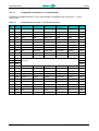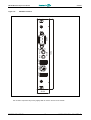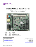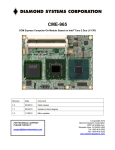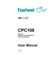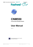
1
CPC504
3U CompactPCI
Intel Core 2 Duo Based
Processor Module
User Manual
Rev. 002a E
October 2011
The product described in this manual is compliant
with all related CE standards.
Product Title:
Document name:
Manual version:
Ref. docs:
CPC504
CPC504 User Manual
002a E
CPC504-UM-v1.05-R
Copyright © 2011 Fastwel Co. Ltd. All rights reserved.
Revision Record
Rev. Index
Brief Description
Product Index
Date
001
Initial preliminary version
CPC504, MIC584, MIC588
October 2010
002
Multiple amendments
CPC504, MIC584, MIC588
September 2011
002a
Reviewed names of connectors
CPC504, MIC584, MIC588
October 2011
Contact Information
Fastwel Co. Ltd
Fastwel Corporation US
Address:
108 Profsoyuznaya st.,
Moscow 117437,
Russian Federation
45 Main Street, Suite 319
Brooklyn, New York 11201
USA
Tel.:
+7 (495) 232-1681
+1 (718) 554-3686
Fax:
+7 (495) 232-1654
+1 (718) 797-0600
Toll free:
E-mail:
[email protected]
Web:
http://www.fastwel.com/
+1 (877) 787-8443 (1-877-RURUGGED)
CPC504
Table of Contents
Table of Contents ..............................................................................................................................................1
List of Tables .....................................................................................................................................................3
List of Figures ....................................................................................................................................................4
Notation Conventions.........................................................................................................................................5
General Safety Precautions................................................................................................................................6
Unpacking, Inspection and Handling...................................................................................................................7
Three Year Warranty..........................................................................................................................................8
1
Introduction...................................................................................................................................... 9
1.1
1.2
1.3
1.4
1.5
1.6
2
Overview ................................................................................................................................................9
CPC504 Versions..................................................................................................................................11
CPC504 Diagrams ................................................................................................................................12
1.3.1
Block Diagram ......................................................................................................................13
1.3.2
Module Appearance..............................................................................................................14
1.3.3
Module Layout ......................................................................................................................17
1.3.4
Module Dimensions...............................................................................................................19
1.3.5
Front Panel...........................................................................................................................21
Technical Characteristics.......................................................................................................................23
1.4.1
Processor, Memory and Chipset............................................................................................23
1.4.2
Interfaces .............................................................................................................................24
1.4.3
Control and Monitoring..........................................................................................................26
1.4.4
General ................................................................................................................................27
1.4.5
Software...............................................................................................................................27
Delivery Checklist..................................................................................................................................28
System Expansion Modules...................................................................................................................28
Detailed Description .......................................................................................................................30
2.1
2.2
2.3
CP C5 0 4
Processor, Memory and Chipset ............................................................................................................30
2.1.1
Processor .............................................................................................................................30
2.1.2
System Memory....................................................................................................................30
2.1.3
Intel® Chipset .......................................................................................................................31
Internal Peripherals ...............................................................................................................................31
2.2.1
Timers ..................................................................................................................................31
2.2.1.1
Watchdog Timer ...................................................................................................32
2.2.2
Battery..................................................................................................................................38
2.2.3
Local SMBus Devices ...........................................................................................................38
2.2.4
Flash Memory.......................................................................................................................39
2.2.4.1
NAND Flash .........................................................................................................39
2.2.4.2
Secure Digital Socket............................................................................................39
2.2.4.3
FRAM Emergency Storage for User Data ..............................................................39
Module Interfaces..................................................................................................................................42
2.3.1
CompactPCI Bus Connectors................................................................................................42
2.3.1.1
CompactPCI Connector Color Coding....................................................................42
2.3.1.2
CompactPCI Connectors J1 and J2 Pinouts...........................................................43
2.3.2
Connectors for Mezzanine Modules.......................................................................................45
2.3.3
Keyboard/Mouse Interface ....................................................................................................46
2.3.4
USB Interfaces......................................................................................................................46
2.3.5
Graphics Controller ...............................................................................................................47
2.3.5.1
DVM Technology ..................................................................................................47
2.3.5.2
Supported Resolutions..........................................................................................47
2.3.5.3
CRT Interface and Connector................................................................................48
2.3.6
Serial Interfaces (RS232 and RS485) ....................................................................................49
2.3.7
Parallel Port Interface............................................................................................................49
Us e r
M a n u a l
1
© 2 0 1 1
F a s t w e l
V e r . 0 0 2 a
E
CPC504
2.3.8
2.3.9
2.3.10
3
Installation.......................................................................................................................................53
3.1
3.2
3.3
3.4
3.5
4
6.2
Temperature Control .............................................................................................................................59
6.1.1
Passive Regulation ...............................................................................................................59
6.1.2
Active Regulation..................................................................................................................60
System Power.......................................................................................................................................60
MIC584 Mezzanine Expansion Module...........................................................................................61
7.1
7.2
7.3
7.4
7.5
8
Boot Details ..........................................................................................................................................58
5.1.1
Booting without a Monitor, Keyboard or Mouse ......................................................................58
5.1.2
Booting from USB .................................................................................................................58
Thermal and Power Issues .............................................................................................................59
6.1
7
PCI Express Operation Modes...............................................................................................................57
Clear CMOS .........................................................................................................................................57
Phoenix® BIOS Setup .....................................................................................................................58
5.1
6
Safety Regulations ................................................................................................................................53
Installation Procedure............................................................................................................................54
Removal Procedure...............................................................................................................................54
Peripheral Devices Installation...............................................................................................................55
3.4.1
USB Devices Installation .......................................................................................................55
3.4.2
Secure Digital Cards Installation............................................................................................55
3.4.3
Battery Replacement.............................................................................................................55
Installation of MIC584 Mezzanine Expansion Module .............................................................................56
Configuration ..................................................................................................................................57
4.1
4.2
5
Gigabit Ethernet....................................................................................................................49
Socket for Secure Digital Card...............................................................................................50
LED Indicators ......................................................................................................................50
2.3.10.1 L2 Indicator Configuration and Control Registers ...................................................51
2.3.10.2 LED Register Initialization .....................................................................................51
2.3.10.3 LED Register Bits .................................................................................................52
Introduction...........................................................................................................................................61
7.1.1
MIC584 Versions ..................................................................................................................61
7.1.2
MIC584 Delivery Checklist ....................................................................................................61
MIC584 Appearance and Layout............................................................................................................62
7.2.1
MIC584 Appearance .............................................................................................................62
7.2.2
MIC584 Components Layout .................................................................................................64
Specifications........................................................................................................................................68
MIC584 Block Diagram..........................................................................................................................69
MIC584 Interfaces.................................................................................................................................70
7.5.1
MIC584 Interfaces List ..........................................................................................................70
7.5.1.1
Front Panel (4HP) Interfaces .................................................................................70
7.5.1.2
Internal Interfaces .................................................................................................70
7.5.2
MIC584 Interfaces Detailed Description .................................................................................71
7.5.2.1
Serial Interfaces....................................................................................................71
7.5.2.2
USB Interfaces .....................................................................................................72
7.5.2.3
PS/2 Keyboard/Mouse Interface............................................................................73
7.5.2.4
Audio Interface .....................................................................................................73
7.5.2.5
L3 and L4 LEDs....................................................................................................74
7.5.2.6
LPT Interface........................................................................................................74
7.5.2.7
SerialATA Interface...............................................................................................75
MIC588 2×DVI Module .....................................................................................................................76
8.1
8.2
8.3
8.4
8.5
CP C5 0 4
Introduction...........................................................................................................................................76
Specifications........................................................................................................................................76
MIC588 Block Diagram..........................................................................................................................77
MIC588 Layout......................................................................................................................................78
DVI-D Connectors .................................................................................................................................79
Us e r
M a n u a l
2
© 2 0 1 1
F a s t w e l
V e r . 0 0 2 a
E
CPC504
9
Supplementary Information............................................................................................................80
9.1
10
Related Standards and Specifications....................................................................................................80
Useful Abbreviations, Acronyms and Short-cuts............................................................................81
List of Tables
Table 1-1:
Table 1-2:
Table 1-3:
Table 2-1:
Table 2-2:
Table 2-3:
Table 2-4:
Table 2-5:
Table 2-6:
Table 2-7:
Table 2-8:
Table 2-9:
Table 2-10:
Table 2-11:
Table 2-12:
Table 2-13:
Table 4-1:
Table 6-1:
Table 7-1:
Table 7-2:
Table 7-3:
Table 7-4:
Table 7-5:
Table 7-6:
Table 7-7:
Table 7-8:
Table 7-9:
Table 7-10:
Table 8-1:
Table 9-1:
Table 9-2:
CP C5 0 4
Us e r
Off-the-Shelf Configurations of CPC504 ......................................................................................11
Dimensions for Different Types of Heatsinks ...............................................................................19
Interface Expansion Modules ......................................................................................................28
SMBus Devices..........................................................................................................................38
CompactPCI Connector Coding Colors .......................................................................................42
CompactPCI Bus Connector J1 (J6) System Slot Pinout ..............................................................43
32-bit CompactPCI Bus Connector J2 (J3) System Slot Pinout.....................................................44
Pinout of J2 Connector for MIC584 Mezzanine Module................................................................45
USB1 and USB2 Pinouts (CPC504 Front Panel)..........................................................................46
Partial List of Supported Display Modes ......................................................................................48
SVGA (J45) Front Panel Connector Pinout..................................................................................48
Gigabit Ethernet Connectors Pinouts...........................................................................................49
L1 and L2 Front Panel Indicators ................................................................................................50
L2 Indicator Configuration and Control Registers .........................................................................51
LED Control Register Bits ...........................................................................................................52
L2 LED Operation Modes ...........................................................................................................52
PCI Express Operation Mode Selection.......................................................................................57
DC Input Voltage Ranges and Limits...........................................................................................60
MIC584 Versions Differences......................................................................................................61
COM1 Serial Port Pinout.............................................................................................................71
RS-232 COM2-COM4 (XP11-XP13) Pinout.................................................................................71
RS-485 COM5 and COM6 (XP7) Pinout......................................................................................72
USB3 and USB4 Connectors Pinout............................................................................................72
PS/2 Connector Pinout ...............................................................................................................73
"LINE_IN" (XP5) Connector Pinout..............................................................................................73
"LINE_OUT" (XP6) Connector Pinout..........................................................................................74
LPT Connector Pinout ................................................................................................................74
SerialATA Connector Pinout .......................................................................................................75
DVI-D Connector Pinout .............................................................................................................79
Related Standards......................................................................................................................80
Related Specifications ................................................................................................................80
M a n u a l
3
© 2 0 1 1
F a s t w e l
V e r . 0 0 2 a
E
CPC504
List of Figures
Figure 1-1:
Figure 1-2:
Figure 1-3:
Figure 1-4:
Figure 1-5:
Figure 1-6:
Figure 1-7:
Figure 1-8:
Figure 1-9:
Figure 1-10:
Figure 1-11:
Figure 1-12:
Figure 2-1:
Figure 2-2:
Figure 2-3:
Figure 2-4:
Figure 2-5:
Figure 2-6:
Figure 3-1:
Figure 7-1:
Figure 7-2:
Figure 7-3:
Figure 7-4:
Figure 7-5:
Figure 7-6:
Figure 7-7:
Figure 7-8:
Figure 7-9:
Figure 7-10:
Figure 7-11:
Figure 7-12:
Figure 7-13:
Figure 7-14:
Figure 8-1:
Figure 8-2:
CPC504 Block Diagram..............................................................................................................13
CPC504 Module Appearance with R2 Heatsink ...........................................................................14
CPC504 Module Appearance Without Heatsink...........................................................................15
CPC504-03 and -04 Bottom Side ................................................................................................16
CPC504 Module Layout: Top Side ..............................................................................................17
CPC504-03 and -04 Module Layout: Bottom Side........................................................................18
CPC504 Module Dimensions with R1 Heatsink............................................................................19
CPC504-01/02 Module Dimensions with R2 Heatsink (8HP) ........................................................20
CPC504-03/04 Module Dimensions with R1 Heatsink and MIC588 ..............................................20
CPC504-03/04 Module Dimensions with R2 Heatsink and MIC588 ..............................................20
CPC504-01/02 4HP Front Panel .................................................................................................21
CPC504-03/04 Front Panel.........................................................................................................22
CompactPCI Connectors J1 and J2 à ........................................................................................42
J2 Expansion Connector for MIC584 Mezzanine Module .............................................................45
USB1 (J22) и USB2 (J16) Sockets..............................................................................................46
SVGA (J45) Front Panel Connector ............................................................................................48
Ethernet Connectors...................................................................................................................49
SD Card Socket .........................................................................................................................50
Fixing of MIC584 on CPC504......................................................................................................56
MIC584 Appearance...................................................................................................................62
MIC584 Appearance with SATA SSD Installed ............................................................................63
MIC584 Components Layout and Dimensions (Top) ....................................................................64
MIC584 Components Layout (Bottom).........................................................................................65
MIC584 with 160 GB SSD Installed.............................................................................................66
MIC584 Front Panel ...................................................................................................................67
CPC504 Block Diagram..............................................................................................................69
COM1 Front Panel Connector.....................................................................................................71
COM2-COM6 Serial Ports IDC2-10 Connector ............................................................................71
USB3 and USB4 Connectors ......................................................................................................72
PS/2 Connector..........................................................................................................................73
LINE_IN (XP5) and LINE_OUT (XP6) Connectors .......................................................................73
LPT Connector (ХР2) .................................................................................................................74
SerialATA Connector..................................................................................................................75
MIC588 Block Diagram...............................................................................................................77
MIC588 Layout (Side Facing CPC504)........................................................................................78
All information in this document is provided for reference only, with no warranty of its suitability for any specific purpose. This information has been thoroughly checked and
is believed to be entirely reliable and consistent with the product that it describes. However, Fastwel accepts no responsibility for inaccuracies, omissions or their
consequences, as well as liability arising from the use or application of any product or example described in this document.
Fastwel Co. Ltd. reserves the right to change, modify, and improve this document or the products described in it, at Fastwel's discretion without further notice. Software
described in this document is provided on an “as is” basis without warranty. Fastwel assumes no liability for consequential or incidental damages originated by the use of
this software.
This document contains information, which is property of Fastwel Co. Ltd. It is not allowed to reproduce it or transmit by any means, to translate the document or to convert
it to any electronic form in full or in parts without antecedent written approval of Fastwel Co. Ltd. or one of its officially authorized agents.
Fastwel and Fastwel logo are trademarks owned by Fastwel Co. Ltd., Moscow, Russian Federation. CompactPCI is a trademark of the PCI industrial Computers
Manufacturers Group. Ethernet is a registered trademark of Xerox Corporation. IEEE is a registered trademark of the Institute of Electrical and Electronics Engineers Inc.
Intel is a trademark of Intel Corporation. Pentium M and Celeron M are trademarks of Intel Corporation. Microsoft is a trademark of the Microsoft corporation. In addition,
this document may include names, company logos and trademarks, which are registered trademarks and, therefore, are property of their respective owners.
Fastwel welcomes suggestions, remarks and proposals regarding the form and the content of this Manual.
CP C5 0 4
Us e r
M a n u a l
4
© 2 0 1 1
F a s t w e l
V e r . 0 0 2 a
E
CPC504
Notation Conventions
Warning, ESD Sensitive Device!
This symbol draws your attention to the information related to electro static sensitivity of your
product and its components. To keep product safety and operability it is necessary to handle
it with care and follow the ESD safety directions.
Warning!
This sign marks warnings about hot surfaces. The surface of the heatsink and some
components can get very hot during operation. Take due care when handling, avoid
touching hot surfaces!
Caution: Electric Shock!
This symbol warns about danger of electrical shock (> 60 V) when touching products or
parts of them. Failure to observe the indicated precautions and directions may expose your
life to danger and may lead to damage to your product.
Warning!
Information marked by this symbol is essential for human and equipment safety.
Read this information attentively, be watchful.
Note...
This symbol and title marks important information to be read attentively for your own benefit.
CP C5 0 4
Us e r
M a n u a l
5
© 2 0 1 1
F a s t w e l
V e r . 0 0 2 a
E
CPC504
General Safety Precautions
This product was developed for fault-free operation. Its design provides conformance to all related
safety requirements. However, the life of this product can be seriously shortened by improper
handling and incorrect operation. That is why it is necessary to follow general safety and
operational instructions below.
Warning!
All operations on this device must be carried out by sufficiently
skilled personnel only.
Warning!
When handling this product, special care must be taken not to hit
the heatsink (if installed) against another rigid object. Also, be
careful not to drop the product, since this may cause damage
to the heatsink, CPU or other sensitive components as well.
Please, keep in mind that any physical damage to this product
is not covered under warranty.
Note:
This product is guaranteed to operate within the published
temperature ranges and relevant conditions. However, prolonged
operation near the maximum temperature is not recommended by
Fastwel or by electronic chip manufacturers due to thermal stress
related failure mechanisms. These mechanisms are common to all
silicon devices, they can reduce the MTBF of the product by
increasing the failure probability. Prolonged operation at the lower
limits of the temperature ranges has no limitations.
Caution, Electric Shock!
Before installing this product into a system and before installing
other devices on it, always ensure that your mains power is switched
off.
Always disconnect external power supply cables during all handling
and maintenance operations with this module to avoid serious
danger of electrical shock.
CP C5 0 4
Us e r
M a n u a l
6
© 2 0 1 1
F a s t w e l
V e r . 0 0 2 a
E
CPC504
Unpacking, Inspection and Handling
Please read the manual carefully before unpacking the module or mounting the device into your
system. Keep in mind the following:
ESD Sensitive Device!
Electronic modules and their components are sensitive to static
electricity. Even a non-perceptible by human being static discharge
can be sufficient to destroy or degrade a component's operation!
Therefore, all handling operations and inspections of this product
must be performed with due care, in order to keep product integrity
and operability:
n
Preferably, unpack or pack this product only at EOS/ESD safe workplaces. Otherwise, it is
important to be electrically discharged before touching the product. This can be done by
touching a metal part of your system case with your hand or tool. It is particularly important
to observe anti-static precautions when setting jumpers or replacing components.
n
If the product contains batteries for RTC or memory back-up, ensure that the module is not
placed on conductive surfaces, including anti-static mats or sponges. This can cause shortcircuit and result in damage to the battery and other components.
Store this product in its protective packaging while it is not used for operational purposes.
n
Unpacking
The product is carefully packed in an antistatic bag and in a carton box to protect it against
possible damage and harmful influence during shipping. Unpack the product indoors only at a
temperature not less than +15°C and relative humidity not more than 70%. Please note, that if the
product was exposed to the temperatures below 0°С for a long time, it is necessary to keep it at
normal conditions for at least 24 hours before unpacking. Do not keep the product close to a heat
source.
Following ESD precautions, carefully take the product out of the shipping carton box. Proper
handling of the product is critical to ensure correct operation and long-term reliability. When
unpacking the product, and whenever handling it thereafter, be sure to hold the module preferably
by the front panel, card edges or ejector handles. Avoid touching the components and connectors.
Retain all original packaging at least until the warranty period is over. You may need it for
shipments or for storage of the product.
Initial Inspection
Although the product is carefully packaged, it is still possible that shipping damages may occur.
Careful inspection of the shipping carton can reveal evidence of damage or rough handling. Should
you notice that the package is damaged, please notify the shipping service and the manufacturer
as soon as possible. Retain the damaged packing material for inspection.
After unpacking the product, you should inspect it for visible damage that could have occurred
during shipping or unpacking. If damage is observed (usually in the form of bent component leads
or loose socketed components), contact Fastwel's official distributor from which you have
purchased the product for additional instructions. Depending on the severity of the damage, the
product may even need to be returned to the factory for repair. DO NOT apply power to the product
if it has visible damage. Doing so may cause further, possibly irreparable damage, as well as result
in a fire or electric shock hazard.
If the product contains socketed components, they should be inspected to make sure they are
seated fully in their sockets.
CP C5 0 4
Us e r
M a n u a l
7
© 2 0 1 1
F a s t w e l
V e r . 0 0 2 a
E
CPC504
Handling
In performing all necessary installation and application operations, please follow only the
instructions supplied by the present manual.
In order to keep Fastwel’s warranty, you must not change or modify this product in any way, other
than specifically approved by Fastwel or described in this manual.
Technical characteristics of the systems in which this product is installed, such as operating
temperature ranges and power supply parameters, should conform to the requirements stated by
this document.
Retain all the original packaging, you will need it to pack the product for shipping in warranty cases
or for safe storage. Please, pack the product for transportation in the way it was packed by the
supplier.
When handling the product, please, remember that the module, its components and connectors
require delicate care. Always keep in mind the ESD sensitivity of the product.
Three Year Warranty
Fastwel Co. Ltd. (Fastwel), warrants that its standard hardware products will be free from defects
in materials and workmanship under normal use and service for the currently established warranty
period. Fastwel’s only responsibility under this warranty is, at its option, to replace or repair any
defective component part of such products free of charge.
Fastwel neither assumes nor authorizes any other liability in connection with the sale, installation
or use of its products. Fastwel shall have no liability for direct or consequential damages of any
kind arising out of sale, delay in delivery, installation, or use of its products.
If a product should fail through Fastwel's fault during the warranty period, it will be repaired free of
charge. For out of warranty repairs, the customer will be invoiced for repair charges at current
standard labor and materials rates.
Warranty period for Fastwel products is 36 months since the date of purchase.
The warranty set forth above does not extend to and shall not apply to:
1.
Products, including software, which have been repaired or altered by other than
Fastwel personnel, unless Buyer has properly altered or repaired the products in
accordance with procedures previously approved in writing by Fastwel.
2.
Products, which have been subject to power, supply reversal, misuse, neglect,
accident, or improper installation.
Returning a product for repair
1.
Apply to Fastwel company or to any of the Fastwel's official representatives for the
Product Return Authorization.
2.
Attach a failure inspection report with a product to be returned in the form, accepted by
customer, with a description of the failure circumstances and symptoms.
3.
Carefully package the product in the antistatic bag, in which the product had been
supplied. Failure to package in antistatic material will VOID all warranties. Then
package the product in a safe container for shipping.
4.
The customer pays for shipping the product to Fastwel or to an official Fastwel
representative or dealer.
CP C5 0 4
Us e r
M a n u a l
8
© 2 0 1 1
F a s t w e l
V e r . 0 0 2 a
E
Introduction
CPC504
1
Introduction
1.1
Overview
The product described in this Manual is CPC504 – a 3U CompactPCI PICMG 2.0 host
processor module based on low power dual-core Intel Сore™ 2 Duo CPUs operating at
1.6 GHz or 2.2 GHz with 4 MB level 2 cache and featuring 800 MHz system bus. The
processor executes up to 8 floating point operations per clock cycle and can address up to
4 GB of soldered DDR2 system memory in 64-bit mode. The list of processors includes
also an ultra low voltage Intel Celeron 573 with 512 KB L2 cache operating at 1 GHz
supporting 533 MHz FSB.
An increased heatsink for CPU and chipset cooling with effective surface area of up to
682 cm2 allows efficient heat dissipation within wide ambient air temperature range.
For high-speed data exchange CPC504 employs two Gigabit Ethernet channels, four x1
PCI Express lanes configurable also as one x4 slot, and 32-bit PCI bus. The integrated
graphics controller of Intel 965GME supports output of two independent video streams to
VGA interface or to two DVI-D interfaces available at MIC588 mezzanine expansion
module.
The firmware of CPC504 supports booting from LAN, from the onboard SD cards, from
soldered 4 GB NAND flash memory disk, or from SATA II (up to 300 MB/s) drives located
on MIC584 mezzanine expansion module or on a rear I/O module.
The MIC584 mezzanine module supports two SATA II interfaces with option to mount
either SATA DOM solid-state modules or one standard 1.8” SATA disk drive. Six COM
ports, two USB 2.0, PS/2, and audio interfaces are available via the MIC584 module as
well.
CPC504 supports FreeDOS, Windows XP Embedded, and Linux 2.6 operating systems.
(TBA)
CP C5 0 4
Us e r
M a n u a l
9
© 2 0 1 1
F a s t w e l
V e r . 0 0 2 a
E
Introduction
CPC504
Some of the CPC504's basic features are:
n
n
n
n
n
n
n
n
n
n
n
n
n
n
n
n
n
n
n
n
n
n
n
n
n
n
4HP, 3U CompactPCI form-factor
Intel® processors:
§
Celeron ULV 573, 1.0 GHz, 512 KB L2 cache, 533 MHz FSB
§
Core™ 2 Duo L7500, 1.6 GHz, 4 MB L2 cache, 800 MHz FSB
§
Core™ 2 Duo T7500, 2.2 GHz, 4 MB L2 cache, 800 MHz FSB
Intel chipset: 82965GME GMCH and ICH8M
Up to 4 GB of soldered dual channel DDR2 SDRAM memory with 64-bit addressing
PCI bus: 32-bit / 33 MHz (System master)
PCI Express: four x1 or one x4 routed to rear I/O (*)
Flash BIOS:
§
SPI interface, 8 Mbit
§
In-system modification
CMOS+SFRAM for configuration parameters storage
FRAM: 31 KB available to user
Watchdog timer:
§
Programmable timeout period
§
NMI, IRQ or Reset signals generation
FPGA firmware upgrade capability
Integrated high performance graphics controller:
§
2D accelerator
§
Up to 384 MB memory shared with system
§
CRT displays support with resolutions of up to 2048×1536, 32 bits at 75 Hz
§
Dual SDVO support, front/rear output capability (*)
§
VGA, two DVI-D interfaces
§
External graphics controller support via x16 PCI-E (*)
Secure Digital card socket
Up to 4 GB soldered NAND flash disk with IDE interface
SATA interface: 3 ports, SATA and SATA II support (*)
Gigabit Ethernet interfaces:
§
Two PCI-E controllers
§
10/100/1000 Mbps
§
Front/rear switchable
USB: 1.1 and 2.0 support, up to five devices (*)
Six serial ports via LPC interface (*)
Parallel port: IEEE1284, ECP/EPP, available at MIC584
HD audio interface; Line In, Line Out, Headphones Out and Mic In (*)
PS/2 keyboard and mouse interface (*)
Real-time clock with battery backup; batteryless operation capability
Self-control and monitoring system
LED indicators
Programmable ejector switch
Phoenix® BIOS
(*) – Available either on the CPC504, on Rear I/O or on mezzanine modules
CP C5 0 4
Us e r
M a n u a l
10
© 2 0 1 1
F a s t w e l
V e r . 0 0 2 a
E
Introduction
1.2
CPC504
CPC504 Versions
At the present time, the module is offered in flexible configuration. The options include different
processors, the size of soldered system memory, and other options described in this section.
Versions -03 and -04 of CPC504 are supplied with MIC588 expansion module (dual DVI-D
interface) installed to the left of processor module.
All variants except C2D2.2 are available in two versions, for industrial (-40°C to +85°C) and for
commercial (0°C to 70°C) temperature ranges. C2D2.2 is available for commercial temperature
range only. At the present time CPC504 is available in the following off-the-shelf configurations:
Table 1-1:
Off-the-Shelf Configurations of CPC504
Configuration
Variants
CPC504-01-C2D1.6-RAM4096-R1-C
CPC504-01-C2D1.6-RAM4096
CPC504-01-C2D1.6-RAM4096-R2-I
CPC504-02-CS1.0-RAM2048-R1-C
CPC504-02-CS1.0-RAM2048
CPC504-02-CS1.0-RAM2048-R1-I
CPC504-02-C2D1.6-RAM2048-R1-C
CPC504-02-C2D1.6-RAM2048
CPC504-02-C2D1.6-RAM2048-R2-I
CPC504-02-C2D2.2-RAM4096
CPC504-02-C2D2.2-RAM4096-R2-C (commercial range only)
PC504-03-C2D2.2-RAM4096
CPC504-03-C2D2.2-RAM4096-R2-С (commercial range only)
CPC504-04-C2D1.6-RAM4096-R1-С
CPC504-04-C2D1.6-RAM4096
CPC504-04-C2D1.6-RAM4096-R2-I
Other configuration options are available upon request. The customer can choose necessary
configuration options using the following template:
1
–
1
2
–
3
–
4
–
5
–
6
\
7
Basic product name:
CPC504
2
3
Version:
Version
NAND Flash 4096
2xDVI-D
01
+
–
02
–
–
03
+
+
04
–
+
Processor:
CS1.0
C2D1.6
C2D2.2
CP C5 0 4
Us e r
M a n u a l
Intel Celeron ULV 573 (512 KB L2 cache, 1.00 GHz, 533 MHz FSB), 10 W
Intel Core 2 Duo L7500 (4 MB L2 cache, 1.6 GHz, 800 MHz FSB), 17 W
Intel Core 2 Duo T7500 (4 MB L2 cache, 2.2 GHz, 800 MHz FSB), 35 W
(C2D2.2 - commercial range only)
11
© 2 0 1 1
F a s t w e l
V e r . 0 0 2 a
E
Introduction
4
CPC504
System memory:
RAM2048
RAM4096
5
2048 MB soldered DDR2 SDRAM
4096 MB soldered DDR2 SDRAM
Heatsinks:
R1
R2
6
Low profile, 4HP
High profile, 8HP
Operating temperature range:
7
C
Commercial, 0°C to +70°C
I
Industrial, -40°C to +85°C
Other options:
Coating
\COATED
Protective Coating
Operating System
\XPE
\LNX
Windows XP Embedded
Linux 2.6
Example:
CPC504 – 01 – CS1.0 – RAM2048 – R1 – C
3U CompactPCI processor module,
4096 MB soldered NAND flash disk,
Intel Celeron ULV 573 CPU (512 KB L2 cache,1.0 GHz, 533 MHz FSB),
2048 MB soldered DDR2 SDRAM,
Low profile heatsink,
Commercial operating temperature range, 0°C to +70°C
1.3
CPC504 Diagrams
The diagrams in this section give visual information about the CPC504 module design, its
appearance, connectors and components layout. The diagrams may not reflect insignificant
differences between the CPC504 versions.
6
CP C5 0 4
Us e r
M a n u a l
12
© 2 0 1 1
F a s t w e l
V e r . 0 0 2 a
E
Introduction
Block Diagram
CPC504 Block Diagram
VGA
HDD, SD
LED
Figure 1-1:
Soldered
DDR II
SDRAM
PCI-Express x16/
SDVO
Intel
Core 2 Duo
Processor
up to 4 GB
SMBus
NAND
Flash
HD Link
Mezzanine Connector
(J1)
Hardware
Monitor
up to 4 GB
LPC
Interface
RST/Power
Switch
GP1, GP2
LEDs
CK-410 &
SS Clocking
10/100/1000
BaseT
SATA
Port 3
965GME
GMCH
VGA
IDE to
NAND
Bridge
USB
Port 5
Gigabit
Ethernet
Controller
10/100/1000
BaseT
GbEthernet
Multiplexor
ICH8M
8 Mbit
Gigabit
Ethernet
Controller
10/100/1000
BaseT
PCI-E Bus
Secure
Digital
Card Socket
PCI-PCI
Bridge
FRAM
Mezzanine Connector (J2)
Power Supply
CP C5 0 4
Us e r
M a n u a l
13
© 2 0 1 1
F a s t w e l
cPCI:J1 (J6)
32-bit PCI Bus
DDR VR
32-bit
PCI Bus
USB
Ports 3, 4
GMCH VR
SATA 1, 2
FPGA
LPC
Interface
CPU Core VR
HD Link
10/100/1000
BaseT
USB
Port 1, 2
USB to
Secure
Digital
Bridge
SPI Flash
BIOS
PCI-E x4
Front Panel
FSB 800 MHz
cPCI:J2 (J3)
1.3.1
CPC504
V e r . 0 0 2 a
E
Introduction
1.3.2
CPC504
Module Appearance
Figure 1-2:
CPC504 Module Appearance with R2 Heatsink
The appearance may vary for different versions of the module.
CP C5 0 4
Us e r
M a n u a l
14
© 2 0 1 1
F a s t w e l
V e r . 0 0 2 a
E
Introduction
Figure 1-3:
CPC504
CPC504 Module Appearance Without Heatsink
The appearance may vary for different versions of the module.
CP C5 0 4
Us e r
M a n u a l
15
© 2 0 1 1
F a s t w e l
V e r . 0 0 2 a
E
Introduction
Figure 1-4:
CPC504
CPC504-03 and -04 Bottom Side
The appearance may vary for different versions of the module.
MIC588 is not shown. Versions -01 and -02 are not equipped with J1 connector.
CP C5 0 4
Us e r
M a n u a l
16
© 2 0 1 1
F a s t w e l
V e r . 0 0 2 a
E
Introduction
1.3.3
CPC504
Module Layout
Figure 1-5:
CPC504 Module Layout: Top Side
Front
Panel
DDR2
SDRAM
Buzzer
GMCH
CPU
J3 (cPCI J2)
CPC504 v.1.0
SVGA
USB1
USB2
Status LEDs
Ethernet
J2
Ejector Handle
NAND Flash
Battery
J18 J6 (cPCI J1)
SD Memory Card
The layout may slightly differ for various versions of the module.
Heatsink is not shown.
CP C5 0 4
Us e r
M a n u a l
17
© 2 0 1 1
F a s t w e l
V e r . 0 0 2 a
E
Introduction
Figure 1-6:
CPC504
CPC504-03 and -04 Module Layout: Bottom Side
PCI-PCI
Bridge
ICH8M
J1
DDR2
SDRAM
The layout may slightly differ for various versions of the module.
MIC588 is not shown. Versions -01 and -02 are not equipped with J1 connector.
CP C5 0 4
Us e r
M a n u a l
18
© 2 0 1 1
F a s t w e l
V e r . 0 0 2 a
E
Introduction
1.3.4
CPC504
Module Dimensions
CPC504 Module Dimensions with R1 Heatsink
130.5
3 max
Figure 1-7:
U27
3 max
U28
165.5
34.7
3.05
A
B
C
211.7
Table 1-2:
Dimensions for Different Types of Heatsinks
Fastwel Code
Heatsink Model & Manufacturer
Type
A
B
C
301415.019
0SX77 AavidThermalloy
R1
17.5
20
20.5
301415.019-02
0SX98 AavidThermalloy
R2
29
31.5
32
301415.019-03
SK463 FischerElektronik
R2
33
35.5
36
301415.019-01
SK120 FischerElektronik
R2
38
40.5
41
CP C5 0 4
Us e r
M a n u a l
19
© 2 0 1 1
F a s t w e l
V e r . 0 0 2 a
E
Introduction
CPC504
CPC504-01/02 Module Dimensions with R2 Heatsink (8HP)
Figure 1-9:
CPC504-03/04 Module Dimensions with R1 Heatsink and MIC588
40,9*
41,1*
35,5*
Figure 1-8:
CPC504-03/04 Module Dimensions with R2 Heatsink and MIC588
40,5*
56,1*
Figure 1-10:
The appearance may vary for different versions of the module.
CP C5 0 4
Us e r
M a n u a l
20
© 2 0 1 1
F a s t w e l
V e r . 0 0 2 a
E
Introduction
1.3.5
CPC504
Front Panel
Figure 1-11:
CPC504-01/02 4HP Front Panel
20.32
19.98
SVGA
Upper Retaining Screw
USB2 USB1
L1
L2
USB Sockets
Eth2
122.4
130.5
SVGA Connector
Status LEDs: L1 and L2
Eth1
Gigabit Ethernet 2 Socket
Gigabit Ethernet 1 Socket
Ejector Handle
Programmable Switch
Lower Retaining Screw
The appearance may slightly differ for various versions of the module.
CP C5 0 4
Us e r
M a n u a l
21
© 2 0 1 1
F a s t w e l
V e r . 0 0 2 a
E
Introduction
L1
USB2 USB1
Eth2
Eth1
DVI2
L2
ACT
SVGA
CPC504-03/04 Front Panel
DVI1
Figure 1-12:
CPC504
40,64*
The appearance may slightly differ for various versions of the module.
The buttons of ejector handles are used to unlock the assembly. Moreover, the right button is a
programmable switch that can be used to initialize the system manually.
CP C5 0 4
Us e r
M a n u a l
22
© 2 0 1 1
F a s t w e l
V e r . 0 0 2 a
E
Introduction
CPC504
1.4
Technical Characteristics
1.4.1
Processor, Memory and Chipset
CPU
CPC504 supports the following Intel processors:
Name
L2 Cache
Clock Speed
FSB Speed
TDP
Intel Celeron ULV 573
512 KB
1.00 GHz
533 MHz
10 W
Intel Core 2 Duo L7500
4 MB
1.6 GHz
800 MHz
17 W
Intel Core 2 Duo T7500
4 MB
2.2 GHz
800 MHz
35 W
System Memory
n
n
n
n
Up to 4 GB of soldered DDR2 SDRAM, w/o ECC
DDR2-667 standard (PC2-5300)
I/O bus clock: 333 MHz
Dual channel mode enabled
Chipset
GMCH: Intel® 82965GME
n
n
n
n
Integrated dual-channel DDR2 memory controller
FSB interface at 800 MHz
Integrated high-performance graphics controller with analog and digital output
Support for external graphics controller with PCI Express x16 interface
Intel® ICH8M I/O Controller Hub
n
n
n
n
n
n
n
n
n
n
n
n
n
n
CP C5 0 4
Us e r
PCI Rev. 2.2 compliant with support for 33 MHz/32-bit PCI bus
Configurable PCI Express interface
Serial ATA II controller, 3 channels
Integrated IDE controller Ultra ATA100, one channel
USB 2.0 host interface, 10 ports
Low Pin Count (LPC) interface
HD-audio interface
SPI bus support
Integrated RTC with CMOS
Power management controller with ACPI and APM support
System Management Bus
Firmware Hub (FWH) interface support
Enhanced DMA controller, interrupt controller, and timer
Additional timers
M a n u a l
23
© 2 0 1 1
F a s t w e l
V e r . 0 0 2 a
E
Introduction
1.4.2
CPC504
Interfaces
CompactPCI Bus Interface
Compliant with CompactPCI Specification PICMG® 2.0 R3.0
n
n
n
n
n
n
System master operation
32-bit / 33 MHz master interface
3.3V / 5.0V compatible
Up to 7 bus master devices
Individual clocks for PCI devices
PCI-PCI bridge asinchronous mode support
PCI Express
n
n
Routed to Rear I/O module connector
Configurable as one x4 or four x1
Serial Ports
n
n
Connectors on mezzanine or Rear I/O module
Realized via LPC interface
Parallel Port
n
n
Connector on MIC584 mezzanine or Rear I/O module
IEEE1284, ECP/EPP
USB Interface
Five USB 2.0 ports:
n
n
n
USB1 and USB2: two Type A connectors on the CPC504 front panel
USB3 and USB4: routed to MIC584 via J2 connector
USB5 available via Rear I/O
Gigabit Ethernet
Two 10/100/1000 Mb/s Gigabit Ethernet interfaces based on the
Intel 82574L GbE PCI Express bus controllers.
n
n
n
n
n
Two RJ45 connectors on the front panel
Switchable between front panel and Rear I/O
Automatic mode recognition
Automatic cabling configuration recognition
Cabling requirement: Category 5, UTP, four-pair cabling
Graphics
Built-in graphics controller
n
n
n
n
n
n
CP C5 0 4
Us e r
High performance Intel® Graphics Media Accelerator (GMA)
Video memory up to 384 MB shared with system
CRT monitors with resolutions of up to 2048 x 1536, 32 bit at 75 Hz
Dual SDVO support, available via two DVI-D connectors at MIC588 module
Video output switchable between front panel and Rear I/O
External graphics controller support via PCI-E x16
M a n u a l
24
© 2 0 1 1
F a s t w e l
V e r . 0 0 2 a
E
Introduction
CPC504
HD Audio
n
n
n
n
n
Realized on mezzanine (MIC584) or on Rear I/O module
Line input/output (optional)
Microphone input
Headphones output
5.1 and 7.1 modes supported
Keyboard and Mouse
n
n
USB KB and MS can be directly connected to CPC504
PS/2 port is available at MIC584 front panel, mouse and keyboard simultaneous
connection is possible via Y-cable
Secure Digital Socket
n
n
Connected to internal USB 2.0 port
Up to 16 GB cards supported
n
n
n
n
Soldered NAND flash disk 4 GB (ver. -01 and -03)
IDE interface (up to 50 MB/s)
Software disconnectable
Can be used as bootable disk
n
n
1 KB is used by the manufacturer
31 available to user
n
n
n
Keyboard controller functionality
LED indicators control
Watchdog timer control
Flash Disk
FRAM
FPGA
SATA Interface
n
n
Three ports: two connectors on mezzanine module, one – on Rear I/O
SATA and SATA II modes supported
Flash BIOS
n
n
CP C5 0 4
Us e r
8 Mb serial EEPROM with SPI interface
In-system modification
M a n u a l
25
© 2 0 1 1
F a s t w e l
V e r . 0 0 2 a
E
Introduction
1.4.3
CPC504
Control and Monitoring
LED Indicators
System status:
n
n
L1: Activity indicator
Yellow: SD memory card
Red: SATA or flash disks
L2:
– Startup process monitoring
– Special system states indication
– Programmable by user
(see details in LED Indicators section)
Gigabit Ethernet status (1 and 2):
n
n
Line (green): Line connected
Act (green): Network activity
Programmable Switch
n
n
Can be used for manual initialization of the system
Integrated into the ejector handle
Thermal Management
Processor is protected from overheating by:
n
n
n
n
Internal processor temperature control unit, which initiates CPU shut down
Processor die temperature monitor
Memory chips temperature monitor
Custom designed heatsinks
Temperature Monitors
n
n
LM87 hardware monitor is used for supervision of the on-die CPU temperature and the
board surface temperature
LM95235 for the memory chips temperature monitoring
Real Time Clock
n
Built in ICH8M
Watchdog Timer
n
n
n
CP C5 0 4
Us e r
Realized in FPGA
Programmable timeout period
Selectable NMI, IRQ, or Reset signals generation
M a n u a l
26
© 2 0 1 1
F a s t w e l
V e r . 0 0 2 a
E
Introduction
1.4.4
CPC504
General
Mechanical
3U CompactPCI form factor
Dimensions:
130.4 × 212.5 × 20.32 mm (5.13” × 8.37” × 0.8”)
Module Weight:
380 g max
Power Supply
+5 V ±5%; +3.3 V ±5% (from CompactPCI connector)
See Section 6.2 for details on power supply requirements
Temperature Ranges
Operational:
CPC504-I
CPC504-C
-40°C ... +85°C
0°C ... +70°C
Storage:
-55°C ... +85°C
Humidity
0 to 80% RH, non-condensing
Battery
3.0 V lithium battery for RTC in a battery holder.
Use Panasonic BR2032 or compatible
1.4.5
Software
Software BIOS
Flash memory based enhanced Phoenix® BIOS has the following features:
n
n
n
n
n
n
n
n
n
n
BIOS boot support for USB keyboards
Software enable/disable function for the Rear I/O, Ethernet, and COM ports configuration
Plug&Play capability
Ethernet boot option
Onboard peripherals enable/disable function
CPU power management features
Programmable handle switch function
Programmable LED control
FRAM enable option
MIC584&MIC588 configuration options
Operating Systems
Supported operating systems:
n
n
n
CP C5 0 4
Us e r
FreeDOS, preinstalled
Microsoft® Windows® XPe
Linux® 2.6
M a n u a l
27
© 2 0 1 1
F a s t w e l
V e r . 0 0 2 a
E
Introduction
1.5
CPC504
Delivery Checklist
The CPC504 delivery set includes:
1.
2.
3.
4.
CPC504 processor module
PCI Express configuration jumper
Antistatic bag
Consumer carton box
Note:
Keep the antistatic bag and the original package at least until
the warranty period is over. It can be used for future storage or
warranty shipments.
1.6
System Expansion Modules
To expand system I/O capabilities Fastwel offers a number of interface modules. Each of these
modules is available in two versions, differing in operating temperature range.
Table 1-3:
Interface Expansion Modules
Name
Description
Connection
MIC584
Mezzanine kit interface module
Via J2 mezzanine connector
MIC588
Mezzanine DVI module
Via J1 mezzanine connector. Installed on CPC504-03/-04
RIO588*
Rear DVI module for MIC588
cPCI connector
(*) The module is developed on order.
MIC584 is a mezzanine interface expansion module. It is designed to be installed on the top side of
CPC504 processor module and is connected via J2 connector. An 1.8” SATA HDD or SSD can be
installed on MIC584 using KIB584 adapter module.
MIC584 has the following interfaces and connectors:
n
n
n
n
n
n
n
CP C5 0 4
Six RS232 and RS485 serial ports – one D-Sub connector on the front panel (COM1)
and four IDC connectors on board
Two USB 2.0 ports (Type A front panel connectors)
One LPT on-board header for connection of a PC-compatible printer or
other devices with parallel interface
Two SerialATA connectors on board
Audio Interface, front panel sockets for connection of a microphone (Mic) and
headphones (Phone) and Line In/Out headers onboard
6-pin PS/2 keyboard/mouse front panel connector
Two LEDs on the front panel
Us e r
M a n u a l
28
© 2 0 1 1
F a s t w e l
V e r . 0 0 2 a
E
Introduction
CPC504
MIC588 mezzanine interface expansion module is designed to be installed on the bottom side of
CPC504 and connected to the processor module via J1 connector (versions -03 and -04). This
module occupies the next slot to the left of CPC504 and is powered via the backplane. Additionally,
they provide possibility to direct video output to the RIO588 rear expansion module.
The detailed description of expansion modules can be found in relevant sections of this Manual.
CP C5 0 4
Us e r
M a n u a l
29
© 2 0 1 1
F a s t w e l
V e r . 0 0 2 a
E
Detailed Description
CPC504
2
Detailed Description
2.1
Processor, Memory and Chipset
2.1.1
Processor
CPC504 can be equipped with the following Intel processors:
Name
L2 Cache
Clock Speed
FSB Speed
TDP
Intel Celeron ULV 573
512 KB
1.0 GHz
533 MHz
10 W
Intel Core 2 Duo L7500
4 MB
1.6 GHz
800 MHz
17 W
Intel Core 2 Duo T7500
4 MB
2.2 GHz
800 MHz
35 W
Supported features of Core™ 2 Duo CPUs are:
n
n
n
n
n
n
n
n
n
n
n
n
Intel® Core™ Microarchitecture
Dual Execution Cores
Intel® EM64T
SSE2, SSE3, SSSE3
Advanced Transfer Cache Architecture
Intel® Dynamic Acceleration
Intel® Thermal monitor with Adaptive Thermal Monitor 2 enhancement
Manufactured on 65 nm process
Enhanced Intel Speedstep® Technology
Dynamic FSB Frequency Switching
Intel® Virtualization Technology
Execute Disable Bit
Intel® Celeron® ULV 573 processor offers low TDP and provides high performance to power
dissipation ratio. Having single core, it has the same microarchitecture and supports virtually the
same main features.
The CPU is soldered to provide excellent shock and vibration stability.
2.1.2
System Memory
Total capacity of the soldered DDR2 SDRAM chips can be up to 4 GB. The installed memory is
DDR2-667 (PC2-5300) compliant and supports PC SPD (Serial Presence Detect) Specification.
Dual channel mode is supported.
CP C5 0 4
Us e r
M a n u a l
30
© 2 0 1 1
F a s t w e l
V e r . 0 0 2 a
E
Detailed Description
2.1.3
CPC504
Intel® Chipset
The chipset consists of the following devices:
n
n
82965GME Graphics and Memory Controller Hub (GMCH)
ICH8M I/O Controller Hub
North Bridge
The 965GME GMCH provides interfaces with the CPU via Front Side Bus (FSB), with dual channel
DDR2 SDRAM system memory, interface to high performance internal graphics controller or
external graphics controller via x16 PCIe link. It also provides DMI interface to the ICH.
The internal graphics controller allows connection of analog and digital displays.
Power management features include ACPI 3.0 support and Dynamic FSB frequency switching.
South Bridge
The ICH8M (82801HBM) is a multifunctional I/O Controller Hub that provides interface to the 32-bit
PCI Bus and configurable PCI Express bus, as well as to such PC interfaces as one UltraDMA100
IDE channel, three SATA II channels, ten USB 2.0 ports, internal real time clock with CMOS,
power controller supporting ACPI and APM. Support for LPC interface, HD audio, and SPI is also
provided.
2.2
Internal Peripherals
The following internal peripherals are available on the CPC504 module:
2.2.1
Timers
CPC504 is equipped with the following timers:
¢ RTC – Real-Time Clock
The ICH contains a MC146818A-compatible real-time clock. The RTC includes 256 bytes of
battery-backed CMOS RAM. The RTC features include timekeeping with alarm function and
100-year calendar, as well as programmable periodic interrupt. A coin-cell battery powers the realtime clock and CMOS memory.
¢ Counters/Timers
Three 8254-type counters/timers integrated in ICH are available on the CPC504.
¢ Additional Timer
The ICH includes an additional programmable timer, which prevents system hang-ups during startups. After the first time-out period is over, it generates the SMI# signal, which starts the software
hang-up recovery subroutine. If the second timeout ends, the "Reset" signal is issued to recover
the system from the hardware hang-up state.
CP C5 0 4
Us e r
M a n u a l
31
© 2 0 1 1
F a s t w e l
V e r . 0 0 2 a
E
Detailed Description
CPC504
¢ Watchdog Timer
The watchdog timer eliminates system hang-ups both during the start-up process (for example, in
case of mistakes in BIOS, when the additional timer is not able to restart the system) and during
normal operation. The timeout period is set in BIOS Setup program. On the expiry of the timeout
period the watchdog timer issues the "Reset" signal or SMI or an interrupt. During start-up process
watchdog timer monitors the BIOS code execution and resets the system in case of activation
error. The instructions on watchdog timer programming can be found in the following subsections.
2.2.1.1
Watchdog Timer
Watchdog timer is realized in FPGA (XC3S250E) as a LPC device. Watchdog timer consists of
24-bit Counter register (Timer Current Value Register) decremented with frequency of 32.768 kHz
and Initial value register (Timer Initial Value Register). On expiry of the timeout period either
interrupt, or SMI, or Reset signal is generated. It is possible to set the timeout period from 0 to 512
seconds with increments of 30.52 ms by changing the decimal value in BIOS Setup.
By default, without prior initialization, the watchdog timeout period is set to maximum that is 512
seconds. The equation below can be used to calculate the timeout TWD in ms as a function of the
decimal value in the Timer Initial Value Register (KWD):
TWD [ms] = KWD * 106 / 215
For example, decimal value "1" of KWD (000001h) corresponds to the timeout of 30.52 ms, and
KWD = 16777215 (FFFFFFh) to 512 seconds.
Strobing of the watchdog timer is performed in one of the following ways:
n
n
n
Writing any value in the Timer Current Value Register
Writing any value in 80h port (this mode is enabled in Timer Init Register)
Writing to or reading from two windows. The address is set in appropriate Window
Base Address registers, the address mask is set in Windows 1&2 Address mask
register, the mode is set in Timer Init Register. The Window size is from 1 to 16 bytes
depending on the value in the Mask register.
Access to Watchdog Registers
The unit's configuration is based on Plug-and-Play architecture. Access to watchdog registers is
available via standard I/O registers (index and data) in configuration mode.
Port
Address
Function
CONFIG PORT
302h
Write
INDEX PORT
302h
Read/Write
DATA PORT
303h
Read/Write
Configuration Mode
To enter the configuration mode write <46h><57h> key to CONFIG PORT. To exit the
configuration mode write <57h><46h> key to CONFIG PORT. INDEX and DATA ports are
available in configuration mode only.
CP C5 0 4
Us e r
M a n u a l
32
© 2 0 1 1
F a s t w e l
V e r . 0 0 2 a
E
Detailed Description
CPC504
Watchdog Timer Programming
The procedures of watchdog programming is described below:
·
Enter configuration mode
MOV
MOV
OUT
MOV
OUT
·
DX,
AL,
DX,
AL,
DX,
Write to LDN register a logic device number (watchdog timer has logical number 1)
MOV
MOV
OUT
MOV
MOV
OUT
·
DX,
AL,
DX,
DX,
AL,
DX,
302H
7
AL
303H
1
AL
Watchdog timer registers are available for read and write now.
For example, to read status register 3Eh and to write the value from it back:
MOV
MOV
OUT
MOV
IN
OUT
·
302H
46H
AL
57H
AL
DX,
AL,
DX,
DX,
AL,
DX,
302H
3EH
AL
303H
DX
AL
To exit configuration mode:
MOV
MOV
OUT
MOV
OUT
DX,
AL,
DX,
AL,
DX,
302H
57H
AL
46H
AL
Global Configuration Registers
Index
Type
Hard Reset
Configuration Register
7h
R/W
01h
Logical Device Number
Logical Device Number register (index 7h)
Index = 7h
Bit
Name
Description
7:0
LDN
Write/Read:
Writing to this register selects logical device.
CP C5 0 4
Us e r
M a n u a l
33
© 2 0 1 1
F a s t w e l
V e r . 0 0 2 a
E
Detailed Description
CPC504
Logical Device 1 Configuration Registers (Watchdog Timer)
Index
I/O Port Address
Type
Hard Reset
Configuration Register
30h
-
R/W
Activate
38h
Base+0
R/W
Timer current value [7:0]
39h
Base+1
R/W
Timer current value [15:8]
3ah
Base+2
R/W
Timer current value [23:16]
3bh
Base+3
R/W
00h
Timer initial value [7:0]
3ch
Base+4
R/W
40h
Timer initial value [15:8]
3dh
Base+5
R/W
00h
Timer initial value [23:16]
3eh
Base+6
R/W
00h
Status register
3fh
Base+7
R/W
03h
Control register
60h
-
R/W
Base[15:8] - I/O port base address
bits [15:8]
61h
-
R/W
Base[7:3] - I/O port base address bits [7:3]
Base[2:0] – should be 0;
70h
-
R/W
00h
Primary interrupt select
F0h
-
R/W
00h
Reserved
F1h
-
R/W
00h
Timer Init Register
F2h
-
R/W
00h
Window 1 base address bits [7:0]
F3h
-
R/W
00h
Window 1 base address bits [15:8]
F4h
-
R/W
00h
Window 2 base address bits [7:0]
F5h
-
R/W
00h
Window 2 base address bits [15:8]
F6h
-
R/W
FFh
Window 1 Mask bits [7:4]
Window 2 Mask bits [3:0]
Activate register
Index = 30h
Bit
Name
Description
7:1
-
Not used
0
Activate
Write/Read:
1 – Current logical device enabled
0 – Current logical device disabled
CP C5 0 4
Us e r
M a n u a l
34
© 2 0 1 1
F a s t w e l
V e r . 0 0 2 a
E
Detailed Description
CPC504
I/O port base address registers
Index = 60h
Bit
Name
Description
7:0
I/O_Base_Adress[15:8]
Write/Read:
Current logical device base address bits 15:8
Index = 61h
Bit
Name
Description
7:0
I/O_Base_Adress[7:0]
Write/Read:
Current logical device base address bits 7:0
Primary interrupt select register
Index = 70h
Bit
Name
Description
7:4
–
Not used
3:0
Interrupt_select
Write/Read:
00h – Interrupt disabled
01h – IRQ1
02h – SMI
03h – IRQ3
04h – IRQ4
05h – IRQ5
06h – IRQ6
07h – IRQ7
08h – IRQ8. Interrupt disabled
09h – IRQ9
0ah – IRQ10
0bh – IRQ11
0ch – IRQ12
0dh – IRQ13. Interrupt disabled
0eh – IRQ14. Interrupt disabled
0fh – IRQ15. Interrupt disabled
CP C5 0 4
Us e r
M a n u a l
35
© 2 0 1 1
F a s t w e l
V e r . 0 0 2 a
E
Detailed Description
CPC504
Timer Init register
Index = F1h
Bit
Name
Description
7:5
–
Not used
P80E
Write/Read:
Counter reset on writing to 80h port
1 – Enabled
0 – Disabled
WND2_WR_EN
Write/Read:
Counter reset on writing cycle to window 2
1 – Enabled
0 – Disabled
WND2_RD_EN
Write/Read:
Counter reset on reading cycle from window 2
1 – Enabled
0 – Disabled
WND1_WR_EN
Write/Read:
Counter reset on writing cycle to window 1
1 – Enabled
0 – Disabled
WND1_RD_EN
Write/Read:
Counter reset on reading cycle from window 1
1 – Enabled
0 – Disabled
4
3
2
1
0
Window 1 port base address registers
Index = F2h
Bit
Name
Description
7:0
Window1_Base_Adress[7:0]
Write/Read:
Bits 7:0 of Window 1 base address
Bit
Name
Description
7:0
Window1_Base_Adress[15:8]
Write/Read:
Bits 15:8 of Window 1 base address
Index = F3h
Window 2 port base address registers
Index = F4h
Bit
Name
Description
7:0
Window2_Base_Adress[7:0]
Write/Read:
Bits 7:0 of Window 2 base address
Bit
Name
Description
7:0
Window2_Base_Adress[15:8]
Write/Read:
Bits 15:8 of Window 2 base address
Index = F5h
CP C5 0 4
Us e r
M a n u a l
36
© 2 0 1 1
F a s t w e l
V e r . 0 0 2 a
E
Detailed Description
CPC504
Windows 1&2 address mask register
Index = F6h
Bit
Name
Description
7:4
Window1_MASK[3:0]
Write/Read:
Bits 3:0 Window 1 address mask
3:0
Window2_MASK[3:0]
Write/Read:
Bits 3:0 Window 2 address mask
WDT Controller I/O Registers
Timer Current Value Register [23:0]
Base+0h
Bit
Name
Description
7:0
Timer_Current_Value[7:0]
Write/Read:
Bits 7:0 of the current timer value
Bit
Name
Description
7:0
Timer_Current_Value[15:8]
Write/Read:
Bits 15:8 of the current timer value
Bit
Name
Description
7:0
Timer_Current_Value[23:16]
Write/Read:
Bits 23:16 of the current timer value
Base+1h
Base+2h
Timer Initial Value Register [23:0]
Base+3h
Bit
Name
Description
7:0
Timer_Initial_Value[7:0]
Write/Read:
Bits 7:0 of the initial timer value
Bit
Name
Description
7:0
Timer_Initial_Value[15:8]
Write/Read:
Bits 15:8 of the initial timer value
Bit
Name
Description
7:0
Timer_Initial_Value[23:16]
Write/Read:
Bits 23:16 of the initial timer value
Base+4h
Base+5h
CP C5 0 4
Us e r
M a n u a l
37
© 2 0 1 1
F a s t w e l
V e r . 0 0 2 a
E
Detailed Description
CPC504
Status Register
Base+6h
Bit
Name
Description
7:3
–
Reserved
2
STM
Write/Read:
Second timeout flag. It is set to “1”, if TMF=1 and RSTE=1.
Cleared by writing “1” into this bit.
1
SME
Read:
SMI enabled on timeout flag. It is set to “1”, if SMI mode is enabled
in Primary interrupt select register (index 70h).
TMF
Write/Read:
Timeout flag. It is set to “1” on expiry of the timeout. This flag
enables interrupt generation. Cleared by writing “1” into this bit, or
by writing to 80h port, or on access to windows 1 or 2 on condition
that one of these modes is enabled.
0
Control Register
Base+7h
Bit
Name
Description
7:3
–
Reserved
1
CNTE
Write/Read:
Writing “1” enables watchdog countdown.
0
RSTE
Write/Read:
Writing “1” enables Reset on timeout.
2.2.2
Battery
The CPC504 utilizes a 3.0 V lithium battery for the RTC and CMOS memory backup. Use
Panasonic BR2032 or compatible. Batteryless operation is possible with no RTC function.
2.2.3
Local SMBus Devices
The CPC504 incorporates a System Management Bus to access several system monitoring and
control devices via a two-wire I2C™ bus interface. The following table presents functions and
addresses of onboard SMBus devices.
Table 2-1:
SMBus Devices
№
SMB Address
Device
1
0D2H
SLG8SP533V System clock generator
2
0A0H and 0A2H
SPD EEPROM module
3
5CH
LM87 PCB & CPU temperature sensor
4
4CH
LM95235 RAM temperature sensor
Upon request, temperature monitors can report information on temperatures of system
components to system control facilities ensuring safe operation.
CP C5 0 4
Us e r
M a n u a l
38
© 2 0 1 1
F a s t w e l
V e r . 0 0 2 a
E
Detailed Description
2.2.4
CPC504
Flash Memory
2.2.4.1
NAND Flash
The CPC504 (versions -01 and -03) is equipped with soldered NAND flash memory modules with
IDE interface (up to 50 MB/s) having total capacity of up to 4 GB for storing user programs and
data. It can be used as a boot disk.
2.2.4.2
Secure Digital Socket
The CPC504 has a standard socket for SD cards connected to an internal USB 2.0 port. Maximum
capacity of SD cards is 16 GB.
2.2.4.3
FRAM Emergency Storage for User Data
Fast serial FRAM (32 KB) is installed on the module. 1 KB is used by manufacturer, 31 KB is
available for storage of critical user data in case of power supply failure. FRAM device registers
and programming is described below.
FRAM Registers (Logical device 3)
Index
I/O Port Address
Type
Hard Reset
Configuration Register
30h
-
R/W
Base+0
R/W
00h
FRAM address value [7:0]
Base+1
R/W
00h
FRAM address value [14:8]
Base+2
R/W
00h
FRAM data value [7:0]
Base+3
R/W
00h
FRAM Control register
[7:1] – reserved
[0] – autoincrement mode
60h
-
R/W
Base[15:8] - I/O port base address
bits [15:8]
61h
-
R/W
Base[7:3] - I/O port base address bits [7:3]
Base[2:0] – must be 0
Activate
To work with FRAM it is necessary to set the base address for the device (LDN=3) and activate it
the same way it is done for the watchdog timer. Subsequent operation is performed in I/O area in
relation to the specified base address. Bit <0> of the Control register (Base+3) enables the
address autoincrement mode for reading from/writing to the Data register (Base+2).
FRAM Programming
The procedures of FRAM programming is described below:
·
Enter configuration mode:
MOV
MOV
OUT
MOV
OUT
CP C5 0 4
Us e r
DX,
AL,
DX,
AL,
DX,
302H
46H
AL
57H
AL
M a n u a l
39
© 2 0 1 1
F a s t w e l
V e r . 0 0 2 a
E
Detailed Description
·
Write to LDN register a logic device number (FRAM has logical number 3):
MOV
MOV
OUT
MOV
MOV
OUT
·
302H
7
AL
303H
3
AL
DX,
AL,
DX,
DX,
AL,
DX,
DX,
AL,
DX,
DX,
AL,
DX,
302H
60H
AL
303H
3H
AL
302H
61H
AL
303H
10H
AL
Activate the device:
MOV
MOV
OUT
MOV
MOV
OUT
·
DX,
AL,
DX,
DX,
AL,
DX,
Set base address for the device in I/O area (for example, 310h):
MOV
MOV
OUT
MOV
MOV
OUT
MOV
MOV
OUT
MOV
MOV
OUT
·
CPC504
DX,
AL,
DX,
DX,
AL,
DX,
302H
30H
AL
303H
1H
AL
To exit configuration mode:
MOV
MOV
OUT
MOV
OUT
DX,
AL,
DX,
AL,
DX,
302H
57H
AL
46H
AL
Further operations with FRAM are performed in I/O area at addresses 310h-313h.
·
Write data byte (32h) to FRAM address 144h:
MOV
MOV
OUT
MOV
MOV
OUT
MOV
MOV
OUT
CP C5 0 4
Us e r
DX,
AL,
DX,
DX,
AL,
DX,
DX,
AL,
DX,
310H
44H
AL
311H
01H
AL
312h
32h
AL
M a n u a l
40
© 2 0 1 1
F a s t w e l
V e r . 0 0 2 a
E
Detailed Description
·
Reading data byte from FRAM address 101h:
MOV
MOV
OUT
MOV
MOV
OUT
MOV
IN
CP C5 0 4
CPC504
Us e r
DX,
AL,
DX,
DX,
AL,
DX,
DX,
AL,
310H
01H
AL
311H
10H
AL
312h
DX
M a n u a l
41
© 2 0 1 1
F a s t w e l
V e r . 0 0 2 a
E
Detailed Description
CPC504
2.3
Module Interfaces
2.3.1
CompactPCI Bus Connectors
22
Figure 2-1:
CompactPCI Connectors J1 and J2 à
J2
The CPC504 is designed for a CompactPCI bus architecture,
but it utilizes only two of standard CompactPCI connectors –
J1 and J2. The CompactPCI standard is electrically identical
to the PCI local bus. However, these systems are improved to
support multiple slots and to operate in harsh industrial
environments.
1
25
J1 stadard CompactPCI connector is marked as J6 on board,
J2 is marked as J3.
J1
2.3.1.1
CompactPCI Connector Color Coding
Guide lugs on CompactPCI connectors serve to ensure a
correct mating of connectors. A proper mating is guaranteed
also by the use of color coded keys for 3.3V and 5V
operation. Color coded keys prevent accidental installation of
a 5V module into a 3.3V slot. CompactPCI backplane
connectors' keying depends always on the signaling (VIO)
level. On universal backplanes supporting both sinalling
levels, VIO level is selected by a jumper on the backplane.
Note:
Pinrows
F and Z
are
GND pins
1
F
E DC BA
Z
CPC504 is a universal module with 3.3V or 5V signalling
voltage level.
Coding key colors are described below:
Table 2-2:
CompactPCI Connector Coding Colors
Voltage Level
Key Color
3.3 V
Cadmium Yellow
5V
Brilliant Blue
Universal module (5V and 3.3V)
None
CompactPCI connector pinouts appear on the following pages.
CP C5 0 4
Us e r
M a n u a l
42
© 2 0 1 1
F a s t w e l
V e r . 0 0 2 a
E
Detailed Description
2.3.1.2
CPC504
CompactPCI Connectors J1 and J2 Pinouts
CPC504 is equipped with two 2´2 mm pitch female CompactPCI bus connectors – J1 (J6)
and J2 (J3).
Table 2-3:
CompactPCI Bus Connector J1 (J6) System Slot Pinout
Pin
Z
A
B
C
D
E
F
25
GND
5V
REQ64#
ENUM#
3.3V
5V
GND
24
GND
AD[1]
5V
LNG_VIO
AD[0]
ACK64#
GND
23
GND
3.3V
AD[4]
AD[3]
LNG_5V
AD[2]
GND
22
GND
AD[7]
GND
LNG_3.3V
AD[6]
AD[5]
GND
21
GND
3.3V
AD[9]
AD[8]
M66EN
C/BE[0]#
GND
20
GND
AD[12]
GND
VIO
AD[11]
AD[10]
GND
19
GND
3.3V
AD[15]
AD[14]
LNG_GND
AD[13]
GND
18
GND
SERR#
GND
3.3V
PAR
C/BE[1]#
GND
17
GND
3.3V
IPMB_SCL
IPMB_SDA
LNG_GND
PERR#
GND
16
GND
DEVSEL#
GND
VIO
STOP#
LOCK#
GND
15
GND
3.3V
FRAME#
IRDY#
SHRT_GND
TRDY#
GND
14
GND
13
GND
12
GND
11
GND
AD[18]
AD[17]
AD[16]
LNG_GND
C/BE[2]#
GND
10
GND
AD[21]
GND
3.3V
AD[20]
AD[19]
GND
9
GND
C/BE[3]#
SHRT_GND
AD[23]
LNG_GND
AD[22]
GND
8
GND
AD[26]
GND
VIO
AD[25]
AD[24]
GND
7
GND
AD[30]
AD[29]
AD[28]
LNG_GND
AD[27]
GND
6
GND
REQ0#
GND
LNG_3.3V
CLK0
AD[31]
GND
5
GND
BRSVP1A5
BRSVP1B5
RST#
LNG_GND
GNT0#
GND
4
GND
IPMB_PWR
HEALTHY#
LNG_VIO
INTP
INTS
GND
3
GND
INTA#
INTB#
INTC#
LNG_5V
INTD#
GND
2
GND
TCK
5V
TMS
TDO
TDI
GND
1
GND
5V
-12V
TRST#
+12V
5V
GND
CP C5 0 4
Us e r
GND
Key Area
GND
GND
M a n u a l
43
© 2 0 1 1
F a s t w e l
V e r . 0 0 2 a
E
Detailed Description
Table 2-4:
CPC504
32-bit CompactPCI Bus Connector J2 (J3) System Slot Pinout
Pin
Z
A
B
C
D
E
F
22
GND
GA4
GA3
GA2
GA1
GA0
GND
21
GND
CLK6
GND
+3.3V
AC_SDIN
AC_BIT_CLK
GND
20
GND
CLK5
GND
AC_SDOUT
AC_RST#
AC_SYNC
GND
19
GND
GND
GND
BP(I/O)
BP(I/O)
BP(I/O)
GND
18
GND
GBE2_MD3N
GBE2_MD1N
GND
PCI_RST#
PCI_SERIRQ
GND
17
GND
GBE2_MD3P
GBE2_MD1P
PRST#
REQ6#
GNT6#
GND
16
GND
GBE2_MD2N
GBE2_MD0N
DEG#
GND
PCI_CLK
GND
15
GND
GBE2_MD2P
GBE2_MD0P
FAL#
REQ5#
GNT5#
GND
14
GND
VGA_BLUE
VGA_HSYNC
GBE1_MD2N
VGA_VSYNC
GBE1_MD0N
GND
13
GND
VGA_GREEN
GBE1_MD3N
GBE1_MD2P
GBE1_MD1N
GBE1_MD0P
GND
12
GND
VGA_RED
GBE1_MD3P
VGA_DDCCLK
GBE1_MD1P
VGA_DDCDAT
GND
11
GND
USB_DATA#
SATA2_RXN
+5V
+5V
SMB_DATA
GND
10
GND
USB_DATA
SATA2_RXP
SATA2_TXN
SMB_CLK
GND
GND
9
GND
LPC_LAD3
LPC_LFRAME#
SATA2_TXP
GND
PE_CLK_N
GND
8
GND
LPC_LAD2
PE4_TN
GND
PE4_RN
PE_CLK_P
GND
7
GND
LPC_LAD1
PE4_TP
PE3_TN
PE4_RP
PE3_RN
GND
6
GND
LPC_LAD0
PE2_TN
PE3_TP
PE2_RN
PE3_RP
GND
5
GND
LPC_LDRQ
PE2_TP
PE1_TN
PE2_RP
PE1_RN
GND
4
GND
V(I/O)
GND
PE1_TP
GND
PE1_RP
GND
3
GND
CLK4
GND
GNT3#
REQ4#
GNT4#
GND
2
GND
CLK2
CLK3
SYSEN#
GNT2#
REQ3#
GND
1
GND
CLK1
GND
REQ1#
GNT1#
REQ2#
GND
CP C5 0 4
Us e r
M a n u a l
44
© 2 0 1 1
F a s t w e l
V e r . 0 0 2 a
E
Detailed Description
2.3.2
CPC504
Connectors for Mezzanine Modules
A number of interface expansion modules are used to enhance I/O capabilities of CPC504.
MIC584 mezzanine module is installed on the top side (to the right) of CPC504 processor module;
60-contact J2 high speed connector socket is used for connection of MIC584.
MIC588 mezzanine module is installed on the bottom side (to the left) of the CPC504 versions -03
and -04 and occupies the backplane connector next to CPC504; 80-contact J1 high-speed
differencial type connector socket is used for connection. The pinout of J1 connector is not
described in this document, since MIC588 and CPC504-03/-04 are supplied bodily.
Figure 2-2:
Table 2-5:
CP C5 0 4
Us e r
J2 Expansion Connector for MIC584 Mezzanine Module
B1
B30
А1
А30
Pinout of J2 Connector for MIC584 Mezzanine Module
Contact
Signal
Contact
Signal
A1
A2
A3
A4
A5
A6
A7
A8
A9
A10
A11
A12
A13
A14
A15
A16
A17
A18
A19
A20
A21
A22
A23
A24
A25
A26
A27
A28
A29
A30
+5V
+5V
USB_PN0
USB_PP0
GND
SATA_TXN0
SATA_TXP0
GND
SATA_TXN1
SATA_TXP1
GND
AZ_BITCLK
GND
AZ_SYNC
AZ_RST#
AZ_SDIN
AZ_SDOUT
+3.3V
KBRST#
A20GATE
+3.3V
PLT_RST#
GND
CLK_33MHz
GND
CLK_14MHz
GND
CLK_32kHz
GND
+5VA
B1
B2
B3
B4
B5
B6
B7
B8
B9
B10
B11
B12
B13
B14
B15
B16
B17
B18
B19
B20
B21
B22
B23
B24
B25
B26
B27
B28
B29
B30
+5V
+5V
USB_PN1
USB_PP1
GND
SATA_RXN0
SATA_RXP0
GND
SATA_RXN1
SATA_RXP1
GND
LPC_AD0
LPC_AD1
LPC_AD2
LPC_AD3
LPC_FRAME#
GND
SERIRQ
+3.3V
DRQ0#
+3.3V
SMB_CLK
SMB_DATA
GND
USB_OC#0
USB_OC#1
+3.3VA
INIT_3V3
BIOS_DIS#
+5VA
M a n u a l
45
© 2 0 1 1
F a s t w e l
V e r . 0 0 2 a
E
Detailed Description
2.3.3
CPC504
Keyboard/Mouse Interface
A keyboard and a mouse can be connected to CPC504 using front panel USB sockets. Moreover,
PS/2 mouse and keyboard can be connected to a standard 6-contact MiniDIN connector on
MIC584 front panel. Mouse and keyboard can be connected simultaneously using Y-cable.
CPC504 includes 8042-compatible keyboard controller emulator realized on FPGA. This is
necessary for correct operation of supported operating systems when CPC504 is used without
MIC584.
2.3.4
USB Interfaces
The CPC504 supports five USB 2.0 ports. Two ports (USB1 and USB2) are available on CPC504
front panel via two Type A connectors. Two ports (USB3 and USB4) are routed to J2 connector
and are available at MIC584 mezzanine module. One more port (USB5) is routed to CompactPCI
connector to be used via a rear I/O module.
USB1 (J22) и USB2 (J16) Sockets
Figure 2-3:
1
2
3
All ports support high-speed, full-speed, and low-speed operation.
Hi-speed USB 2.0 supports data transfer rate of up to 480 Mb/s.
One USB device may be connected to each port. To connect more
than five USB devices use an external hub.
4
The USB power supply is protected by a self-resettable 500 mA
fuse.
Table 2-6:
USB1 and USB2 Pinouts (CPC504 Front Panel)
Pin Number
Signal
Function
In/Out
1
VCC
VCC signal
–
2
UV0-
Differential USB-
–
3
UV0+
Differential USB+
–
4
GND
GND signal
–
CP C5 0 4
Us e r
M a n u a l
46
© 2 0 1 1
F a s t w e l
V e r . 0 0 2 a
E
Detailed Description
2.3.5
CPC504
Graphics Controller
A highly integrated 2D/3D graphics accelerator is included in the 965GME chipset. The internal
graphics controller provides interfaces to a standard analog monitor (SVGA connector on CPC504
front panel) or/and to a digital displays. External video adapters with PCI Express x16 interface are
supported.
Integrated 2D/3D Graphics features:
n
n
n
n
n
n
2D accelerator
Up to 384 MB video memory shared with system
Support for RGB monitors with resolutions up to 2048´1536, 32 bit at 75 Hz
Dual DVI support, possibility to switch graphics output to rear panel
Support for external video adapters with PCI-E x16 interface
Support for DirectX 10.0, Open GL 2.0, Shader Model 4.0:
§
Core frequency up to 333 MHz;
§
Rendering frequency up to 500 MHz
2.3.5.1
DVM Technology
The 965GME chipset supports the Dynamic Video Memory Technology (DVMT). This technology
provides use of all available memory in the most efficient way for maximum graphics performance.
DVMT dynamically responds to requests from applications allocating the required amount of video
memory. The Intel® 965GME graphics driver is allowed to request up to 384 MB of system
memory. When not needed by the graphics subsystem, the memory is freed up for other
applications. Thus, memory usage is balanced for optimal graphics and system memory
performance.
To support legacy VGA devices the internal video-controller needs at least 1 MB of system
memory. Thus, the reported system memory size is always 1 MB less than available amount of
physical memory.
2.3.5.2
Supported Resolutions
The integrated 400 MHz RAMDAC of the 965GME chipset allows direct connection of a
progressive scan analog monitor with a resolution of up to 2048 ´ 1536 at 75 Hz. The supported
resolution depends on the color depth and on the vertical scanning frequency, as illustrated in the
table below.
CP C5 0 4
Us e r
M a n u a l
47
© 2 0 1 1
F a s t w e l
V e r . 0 0 2 a
E
Detailed Description
Table 2-7:
CPC504
Partial List of Supported Display Modes
Color Resolution vs. Vertical Frequency
Display Mode
8-bit Indexed
16- bit
32- bit
60
75
85
100
60
75
85
100
60
75
85
100
640 ´ 480
´
´
´
´
´
´
´
´
´
´
´
´
800 ´ 600
´
´
´
´
´
´
´
´
´
´
´
´
1024 ´ 768
´
´
´
´
´
´
´
´
´
´
´
´
1280 ´ 1024
´
´
´
´
´
´
´
´
´
´
´
´
1600 ´ 1200
´
´
´
´
´
´
´
´
´
´
´
´
1920 ´ 1440
´
´
´
´
´
´
´
´
´
2048 ´ 1536
´
´
´
´
´
´
2.3.5.3
CRT Interface and Connector
Figure 2-4:
SVGA (J45) Front Panel Connector
6
1
11
The 15-pin female D-Sub connector (J45) on CPC504 front panel is
used to connect a CRT monitor to the CPC504 module.
Its pinout is in the table below.
5
10
Table 2-8:
15
SVGA (J45) Front Panel Connector Pinout
Pin Number
Signal
Function
In/Out
1
Red
Red video signal output
Out
2
Green
Green video signal output
Out
3
Blue
Blue video signal output
Out
9
VCC
Power +5V DC 200 mA
Out
12
DDCdata
I2C™ data
In/Out
13
Hsync
Horizontal sync.
TTL out
14
Vsync
Vertical sync.
TTL out
2
15
DDCclk
I C™ clock
Out
5, 6, 7, 8, 10
GND
Signal ground
–
4, 11
–
Free (reserved)
–
CP C5 0 4
Us e r
M a n u a l
48
© 2 0 1 1
F a s t w e l
V e r . 0 0 2 a
E
Detailed Description
2.3.6
CPC504
Serial Interfaces (RS232 and RS485)
Serial interfaces are available only on MIC584 interface expansion module. There are six serial
ports available via MIC584 connectors:
n
n
n
COM1 – RS232, 9-pin D-Sub front panel connector;
COM2-COM4 – RS232, three IDC2-10 onboard connectors (XP11-XP13);
COM5, COM6 – RS485, one IDC2-10 onboard connector (XP7).
All COM ports are fully compatible with the 16C550 controller and include a complete set of
handshaking and modem control signals, maskable interrupt generation and data transfer of up to
460.8 Kb/s.
2.3.7
Parallel Port Interface
Standard parallel port (IEEE1284, SPP/ECP/EPP) is available only on MIC584 mezzanine module.
2.3.8
Gigabit Ethernet
The CPC504 board includes two 10Base-T/100Base-TX/1000Base-T Ethernet ports based on
Intel® 82574L Gigabit Ethernet PCI-E bus controllers. The Intel® 82574L Gigabit Ethernet
controller architecture combines high performance and low power consumption. The controller's
features include independent transmit and receive queues to limit PCI-E bus traffic, and a PCI-E
interface providing efficient bus utilization by increased use of bursts.
Figure 2-5:
Act
Ethernet Connectors
Link
Two RJ45 Gigabit Ethernet connectors are located on CPC504
front panel (J24).
The interfaces provide auto-detection and switching between
10Base-T, 100Base-TX and 1000Base-T operation modes.
1
1
Each of the two Ethernet channels may be software switched to rear I/O to provide system
flexibility.
Table 2-9:
Gigabit Ethernet Connectors Pinouts
10Base-T
100Base-TX
1000Base-T
Pin
I/O
Signal
I/O
Signal
I/O
Signal
1
O
TX+
O
TX+
I/O
BI_DA+
2
O
TX–
O
TX–
I/O
BI_DA–
3
I
RX+
I
RX+
I/O
BI_DB+
4
–
–
–
–
I/O
BI_DC+
5
–
–
–
–
I/O
BI_DC–
6
I
RX–
I
RX–
I/O
BI_DB–
7
–
–
–
–
I/O
BI_DD+
8
–
–
–
–
I/O
BI_DD–
MDI / Standard Ethernet Cable
CP C5 0 4
Us e r
M a n u a l
49
© 2 0 1 1
F a s t w e l
V e r . 0 0 2 a
E
Detailed Description
CPC504
Integrated Ethernet LEDs
Line (green): This LED indicates network connection. The LED lights up when the line is
connected.
Act (green): this LED monitors network activity. The LED lights up when network packets are sent
or received through the RJ45 port. When this LED is not lit, it means that the computer is not
sending or receiving network data.
2.3.9
Socket for Secure Digital Card
Figure 2-6:
SD Card Socket
To enable usage of SD memory cards CPC504 has a Secure
Digital card socket (J12) on board.
SD interface is connected to an internal USB 2.0 port via SMSC
USB2241 controller. SD cards with maximum capacity of 16 GB
are supported.
2.3.10
LED Indicators
Two LED indicators L1 and L2 are located on the CPC504 front panel.
Table 2-10:
L1 and L2 Front Panel Indicators
Name
Purpose
Color
Function
L1
Activity indicator
Yellow
SD memory card activity
Red
SATA or Flash drive activity
Green, fast blinking (8 Hz)
The module is powered. The system is
activated
Green, slowly blinking (1 Hz)
POST (Power-On Self Test) in process
Green, steady light
OS is being loaded
Red, steady light
Activation error
(wrong slot, incomplete insertion of the
module, power supply failure)
Red, fast blinking (8 Hz)
Clear CMOS mode activated, pending
Programmable switch release
Orange, steady light
S5 (soft off) mode.
The active mode is enabled by momentary
pressing on Programmable switch.
Orange, slowly blinking
(0.5 Hz)
S3 (Suspend-To-RAM) mode.
The active mode is enabled by momentary
pressing on Programmable switch.
L2
CPC504 boot process
monitoring
System state
indication
Programmed by user
After initialization and OS loading, L2 indicator can be used as programmable LED. L2 modes
programming is described below.
CP C5 0 4
Us e r
M a n u a l
50
© 2 0 1 1
F a s t w e l
V e r . 0 0 2 a
E
Detailed Description
2.3.10.1
CPC504
L2 Indicator Configuration and Control Registers
Table 2-11:
L2 Indicator Configuration and Control Registers
Index
I/O Port Address
Type
Hard Reset
Configuration Register
30h
-
R/W
00h
Activate. Bit[0] to «1» – LED module is
active.
-
Base+0
R/W
01h
LED data register [3:0].
The rest bits are nonsignificant;
are read as «0».
60h
-
R/W
Base[15:8] - I/O port base address
bits[15:8]
61h
-
R/W
Base[7:0] - I/O port base address bits[7:0]
To work with L2 indicator it is necessary to set the base address for the device (LDN=5) and
activate it as it is done for the watchdog timer or FRAM module. L2 indicator is controlled via LED
register. Subsequent operation is performed in I/O area in relation to the specified base address.
2.3.10.2
LED Register Initialization
To initialize the register follow the following procedure:
·
Enter configuration mode:
MOV
MOV
OUT
MOV
OUT
·
DX,
AL,
DX,
DX,
AL,
DX,
302H
7
AL
303H
5
AL
Set base address for the device in I/O area (for example, 31dh):
MOV
MOV
OUT
MOV
MOV
OUT
MOV
MOV
OUT
MOV
MOV
OUT
CP C5 0 4
302H
46H
AL
57H
AL
Write to LDN register a logic device number (LED register has logical number 5):
MOV
MOV
OUT
MOV
MOV
OUT
·
DX,
AL,
DX,
AL,
DX,
Us e r
DX,
AL,
DX,
DX,
AL,
DX,
DX,
AL,
DX,
DX,
AL,
DX,
302H
60H
AL
303H
3H
AL
302H
61H
AL
303H
1dH
AL
M a n u a l
51
© 2 0 1 1
F a s t w e l
V e r . 0 0 2 a
E
Detailed Description
·
Activate the device:
MOV
MOV
OUT
MOV
MOV
OUT
·
DX,
AL,
DX,
DX,
AL,
DX,
302H
30H
AL
303H
1H
AL
To exit configuration mode:
MOV
MOV
OUT
MOV
OUT
2.3.10.3
DX,
AL,
DX,
AL,
DX,
302H
57H
AL
46H
AL
LED Register Bits
Table 2-12:
Bit7
CPC504
Bit6
LED Control Register Bits
Bit5
Bit4
Reserve bits are read as "0".
Bit3
Bit2
Bit1
Bit0
Red LED
Bit1
Red LED
Bit0
Green LED
Bit1
Green LED
Bit0
L2 LED indicator consists of two independent red and green LEDs. Thus, it can glow green, red
or orange (red and green are both on). Each LED is independently controlled via the LED register
bits. Operation mode for each LED is set by values in two bits as shown in the table below.
Table 2-13:
L2 LED Operation Modes
Bit1
Bit0
Operation Mode
0
0
LED is off
0
1
Fast blinking (8 Hz)
1
0
Slow blinking (1 Hz)
1
1
Steady light
CP C5 0 4
Us e r
M a n u a l
52
© 2 0 1 1
F a s t w e l
V e r . 0 0 2 a
E
Installation
3
CPC504
Installation
The CPC504 is easy to install. However, it is necessary to follow the procedures and safety
regulations below to install the module correctly without damage to the hardware, or harm to
personnel.
The installation of the peripheral drivers is described in the accompanying information files. For
details on installation of an operating system, please refer to the relevant software documentation.
3.1
Safety Regulations
The following safety regulations must be observed when installing or operating the CPC504.
Fastwel assumes no responsibility for any damage resulting from infringement of these rules.
Warning!
When handling or operating the module, special attention should be
paid to the heatsink, because it can get very hot during operation.
Do not touch the heatsink when installing or removing the module.
Moreover, the module should not be placed on any surface or in any
kind of package until the module and its heatsink have cooled down
to ambient temperature.
Caution!
If your module does not allow hotswapping, switch off the system
power before installing the module in a free slot. Disregarding this
requirement could be harmful for your life or health and can damage
the module or entire system.
ESD Sensitive Equipment!
This product comprises electrostatically sensitive components.
Please follow the ESD safety instructions to ensure module's
operability and reliability:
n
n
Use grounding equipment, if working at an anti-static
workbench. Otherwise, discharge yourself and the tools
in use before touching the sensitive equipment.
Try to avoid touching contacts, leads and components.
Extra caution should be taken in cold and dry weather.
CP C5 0 4
Us e r
M a n u a l
53
© 2 0 1 1
F a s t w e l
V e r . 0 0 2 a
E
Installation
CPC504
3.2
Installation Procedure
To install CPC504 in a system, follow the instructions below.
1.
Keep to the safety regulations of the Section 3.1 when performing the following
operations.
Warning!
Failure to accomplish the following instruction may damage the
module or result in incorrect system operation.
2.
Ensure that the module configuration corresponds to the application requirements before
installing. For information regarding the configuration of the CPC504, refer to Chapter 4.
For the installation of CPC504 specific peripheral devices and I/O devices refer to the
appropriate sections in Chapter 3. For details on installation of expansion modules, refer
to respective sections of this document.
3.
To install the CPC504:
1.
Make sure that no power is connected to the system.
2.
Avoiding contact with other modules of the system, carefully insert the module into
the chosen slot until it contacts the backplane connectors. Do not apply force
pushing the module into the backplane connectors.
3.
Using the front panel ejector handle, engage the module with the backplane. The
module is completely engaged, when the ejector handle is locked. For versions -03
and -04 ensure simultaneous locking of both handles.
4.
Fix the module with the front panel retaining screws.
5.
Connect the required external interfacing cables to the module's connectors and
make sure that the module and all connected cables are properly fixed.
The CPC504 is now ready for operation. Please, refer to appropriate software, application, and
system manuals to get further instructions.
3.3
Removal Procedure
To remove the module from the system case do the following:
1.
When performing the next actions, keep to safety regulations of the Section 3.1.
Pay special attention to the temperature of the heatsink!
2.
Ensure that the system power is switched off before proceeding.
3.
Disconnect all cables that may be connected to the module.
4.
Unscrew the front panel retaining screws.
5.
Unlock the module ejection handle(s) by pressing the integrated button(s), and then press
on the handle(s) until the module connectors are disconnected from the backplane.
6.
Carefully pull the module out of the slot. Do not touch the heatsink, since it can get very
hot during operation.
7.
Dispose of the module at your discretion. The module should not be placed on any
surface or in any form of package until the board and the heatsink have cooled down to
room temperature.
CP C5 0 4
Us e r
M a n u a l
54
© 2 0 1 1
F a s t w e l
V e r . 0 0 2 a
E
Installation
3.4
CPC504
Peripheral Devices Installation
A lot of peripheral devices can be connected to the CPC504. Their installation procedures differ
significantly. Therefore the following sections provide mainly general guidelines regarding
installation of peripheral devices.
3.4.1
USB Devices Installation
The CPC504 can accept Plug&Play connection of USB 2.0 computer peripheral devices (printers,
keyboards, mice, etc.) All USB devices may be connected or disconnected while the host power is
on.
3.4.2
Secure Digital Cards Installation
SD socket of CPC504 (J12) supports SD cards with operating voltage of 3.3 V.
Note:
SD cards may be connected or disconnected while the system
power is on.
Carefully slide in the correctly oriented card and gently press to engage the contacts completely.
Please remember that the heatsink may be hot after operation.
Note:
It is recommended to use SD cards, which has been initialized and
formatted in this module.
3.4.3
Battery Replacement
The lithium battery must be replaced with Panasonic BR2032 or a battery with similar
characteristics.
The expected life of a 190 mAh battery in case of operation for 8 hours a day at 30°C is about
5 years. However, this typical value may vary because battery life depends on the operating
temperature and the shutdown time of the system in which the battery is installed.
Note...
It is recommended to replace the battery after approximately 4 years
to be sure it is operational.
Important:
Replacing the battery, make sure the polarity is correct ("+" up).
Dispose of used batteries according to the local regulations.
CP C5 0 4
Us e r
M a n u a l
55
© 2 0 1 1
F a s t w e l
V e r . 0 0 2 a
E
Installation
3.5
CPC504
Installation of MIC584 Mezzanine Expansion Module
Figure 3-1:
Fixing of MIC584 on CPC504
A
B
D
J2
C
To install MIC584 mezzanine expansion module on CPC504 do the following:
1.
Unscrew the В and С screws fixing the heatsink.
2.
Install standoffs into A, B, C, and D openings.
3.
Install MIC584 module engaging its XS6 connector with J2 connector of CPC504
and fix with screws at positions A, B, C, and D.
The details on connection of external devices to MIC584 module can be found in Section 7 of this
manual.
CP C5 0 4
Us e r
M a n u a l
56
© 2 0 1 1
F a s t w e l
V e r . 0 0 2 a
E
Configuration
CPC504
4
Configuration
4.1
PCI Express Operation Modes
J18 jumper located on the top side of the CPC504 module is used for switching between two
PCI Express operation modes – one х4 link or four х1.
Table 4-1:
PCI Express Operation Mode Selection
J18
4.2
Contacts
PCI Express Lanes Configuration
Closed
One х4
Open
Four х1
Clear CMOS
If the system is not booted (for example, due to incorrect BIOS settings), it is possible to clear
BIOS Setup parameters stored in CMOS memory using Programmable switch. To clear CMOS
memory, follow the procedure below:
1.
2.
3.
4.
5.
CP C5 0 4
Switch power off.
Press the button «Programmable switch» on the ejector handle and slightly open the
ejector handle but do not move the module out of its slot.
Switch power on.
Wait until L2 red LED starts blinking fast and move the ejector handle back to the locked
position by lifting it until the click.
Start BIOS Setup utility (F2) to configure the system.
Us e r
M a n u a l
57
© 2 0 1 1
F a s t w e l
V e r . 0 0 2 a
E
Phoenix® BIOS Setup
5
CPC504
Phoenix® BIOS Setup
The Phoenix® BIOS in your SBC is an adapted version of a standard BIOS for IBM PC
AT-compatible personal computers equipped with Intel®x86 and compatible processors. The BIOS
provides low-level support for the central processing, memory, and I/O system units.
With the help of BIOS Setup program, you can modify the BIOS configuration parameters and
control the special features of your module. The Setup program is started by pressing the F2 key
and offers a convenient menu interface to modify basic system configuration settings and switching
between the subsystems operation modes. These settings are stored in a dedicated batterybacked memory, CMOS RAM, that keeps the information when the power is switched off. For
increased security, the CMOS data and some of the service parameters are stored also in a
nonvolatile serial EEPROM memory. This allows to restore the critical data in emergency cases
after battery failure.
5.1
Boot Details
5.1.1
Booting without a Monitor, Keyboard or Mouse
To boot without a monitor, keyboard or mouse set the item "POST Errors" to "Disabled" at the
page "Main" in PhoenixBIOS Setup program. This setting is a default one.
Note!
If the module was booted without a connected monitor, the display
will be empty, even if a monitor is connected later during operation.
To get the correct display output it is necessary to reboot the module
with a connected monitor. This is a Intel VideoBIOS particularity.
5.1.2
Booting from USB
To boot from a device connected to USB:
n
n
n
n
Connect the device to boot from to a USB port. The appropriate USB controller should
be enabled;
Enter the PhoenixBIOS Setup program;
Find this USB device at the "Boot" page and use «+» «–» buttons to move it in order to
change its boot priority;
Save changes and reboot the module.
To get the on-line help about the details of BIOS Setup program operation, please apply to the
screen tips and the integrated help system.
CP C5 0 4
Us e r
M a n u a l
58
© 2 0 1 1
F a s t w e l
V e r . 0 0 2 a
E
Thermal and Power Issues
CPC504
6
Thermal and Power Issues
6.1
Temperature Control
Intensive operation of Intel Core 2 Duo processor in harsh environment requires a special
technology to keep the processor’s die temperature within allowed limits. The following sections
provide system integrators with the information, which will help to meet thermal requirements when
developing systems based on CPC504.
6.1.1
Passive Regulation
The thermal management concept of CPC504 module includes several separate but correlated
functions. Their main purpose is to protect the processor from overheating and reduce its power
consumption. Dedicated thermal control subsystem allows the processor to operate within safe
temperature range without the need for special software or interrupt handling.
1.
Catastrophic Shutdown Detector technology allows to automatically switch the
processor off when the processor die temperature reaches approximately 125°C due to,
for example, the cooling system failure. The catastrophic shutdown detector is based on
an internal thermal diode used to detect internal core processor temperature. This function
is always active to protect the processor in any case. Processor execution is halted until
the next reset cycle. Once this function is activated, the system does not return to the
normal operation mode automatically, it is necessary to reset the BIOS settings and to
cold restart the system.
2.
The Intel® Core 2 Duo processor supports the Enhanced Intel SpeedStep® technology.
It allows to dynamically switch the processor core voltage and frequency without resetting
the system, when the processor core temperature reaches 100°C. For example, the Core
2 Duo L7500 processor operating at 1.6 GHz and 1.2 V can be switched down to
800 MHz and 0.95 V, thus reducing the processor power dissipation.
External thermal monitor (LM87) gathers information about the processor and board
surface temperatures from two sensors. One additional thermal monitor is used to watch
the memory modules temperature. This information may then be requested by a program
to undertake the appropriate actions.
4.
Recommendations
Generally, there is no need to enable the Thermal Management functions if the module is operated
in a optimally designed environment with sufficient air flow. However, to guarantee a stable system
in unsteady industrial environment, both the internal and the external thermal monitors should be
enabled. These two monitors protect the processor and the whole system against overheating.
Note:
Thermal Management functions should be disabled when performing
Benchmarks and performance tests, otherwise the results will be
incorrect due to the power reduction processes influence.
CP C5 0 4
Us e r
M a n u a l
59
© 2 0 1 1
F a s t w e l
V e r . 0 0 2 a
E
Thermal and Power Issues
6.1.2
CPC504
Active Regulation
To provide controlled active heat dissipation CPC504 is equipped with a specially designed
heatsinks. Together with a system chassis with adjustable forced air flow capability this provides a
basis for reliable and steady operation. Forced air flow of sufficient volume is vital for high
performance processors operating in high temperature environments.
When developing applications using the CPC504, the system integrator must take into account the
overall system thermal requirements. System chassis must satisfy these requirements. When
performing thermal calculations for certain application, the developer must consider the
contribution of peripherals to be used with the CPC504 to the total heat emission. These devices
must also be capable to operate at the temperatures within the system operating range, especially
those, which are attached directly to the CPC504 processor module.
Warning!!!
Since Fastwel does not assume responsibility for any damage to the
CPC504 module or other system parts resulting from overheating of
the central processor, it is important to ensure that the CPC504
operational environment parameters conform to the thermal
requirements described in this Manual.
6.2
System Power
The Intel Core 2 Duo processor family require special characteristics of the power supply unit and
the backplane.
The CPC504 module itself has been designed to provide best possible power supply for each
system unit. However, in order to guarantee reliable and faultless operation the following
requirements must be taken into account. Absolute maximum input voltages presented in the table
below must not be exceeded to guarantee that the CPC504 is not damaged. The ranges for the
different input power voltages, within which the module is functional, are also presented.
Table 6-1:
DC Input Voltage Ranges and Limits
Power Voltage, V
Maximum Permitted Value, V
Recommended Range, V
+3.3
+3.6
3.135
to
3,465
+5
+5.5
4.75
to
5.25
Power supplies to be used with the CPC504 should comply with these requirements.
Only backplanes which have two power layers for each of the +3.3V and the +5V supply voltage
are recommended for CPC504. Input power connections to the backplane itself should provide
minimum power loss. Avoid using long input lines, low carrying capacity cables, high resistance
connections.
To select the appropriate system power supply, it is necessary to consider the CPC504 own power
consumption (about 35 watts), the consumption of the remaining system components, possible
variations of power consumption during operation (e.g. due to temperature changes) and some
reserve. Taking all this into account, it is recommended to use a 150 watt power supply. If possible,
power supplies with voltage sensing should be used. This may require an appropriate backplane.
Consumption currents for CPC504 are: +3.3 V – 2 A, +5 V – 6 A.
CP C5 0 4
Us e r
M a n u a l
60
© 2 0 1 1
F a s t w e l
V e r . 0 0 2 a
E
MIC584 Mezzanine Expansion Module
CPC504
7
MIC584 Mezzanine Expansion Module
7.1
Introduction
MIC584 mezzanine expansion module is designed for installation on Fastwel's CPC504
CompactPCI 3U processor module. This mezzanine I/O module expands functionality and I/O
capability of the CPC504. MIC584 module is installed on the top side of the CPC504 processor
module and connected via the J2 connector.
7.1.1
MIC584 Versions
At the present time the module is supplied in two versions: MIC584-01-I and MIC584-01-C. They
have the same functionality, and differ in the operating temperature range, as shown in the table
below:
Table 7-1:
MIC584 Versions Differences
Operating Temperature Range, °С
Version (Order Code)
MIC58401-I
MIC58401-C
-40
to
+85
0
to
+70
Protective coating can be applied as an option (\COATED).
7.1.2
MIC584 Delivery Checklist
The MIC584 supplied set includes:
1.
MIC584 mezzanine module
2.
PS/2 Y-cable
3.
Two SATA data cables
4.
SATA power cable
5.
Two jumpers for ХР3, ХР4
6.
MIC584 and HD mounting kit
7.
Antistatic bag for MIC584
8.
Consumer package
Note:
Keep all the original packaging material (antistatic bag and
consumer package) for future storage or warranty shipments.
CP C5 0 4
Us e r
M a n u a l
61
© 2 0 1 1
F a s t w e l
V e r . 0 0 2 a
E
MIC584 Mezzanine Expansion Module
7.2
CPC504
MIC584 Appearance and Layout
The figures in this section are supposed to help you to locate and identify the module's
components and connectors. Our constant efforts in improving our products may result in minor
differences between the real module and its depictions.
7.2.1
MIC584 Appearance
Figure 7-1:
MIC584 Appearance
The appearance of your product may slightly differ from the shown above.
CP C5 0 4
Us e r
M a n u a l
62
© 2 0 1 1
F a s t w e l
V e r . 0 0 2 a
E
MIC584 Mezzanine Expansion Module
Figure 7-2:
CPC504
MIC584 Appearance with SATA SSD Installed
Draft. The appearance of your product may slightly differ from the shown above.
CP C5 0 4
Us e r
M a n u a l
63
© 2 0 1 1
F a s t w e l
V e r . 0 0 2 a
E
MIC584 Mezzanine Expansion Module
7.2.2
CPC504
MIC584 Components Layout
Figure 7-3:
MIC584 Components Layout and Dimensions (Top)
100
2
1
10
0
9
2
1
10
9
2
1
10
9
2
1
10
9
MIC584
88.3
The module's components layout may slightly differ for various versions of the module.
CP C5 0 4
Us e r
M a n u a l
64
© 2 0 1 1
F a s t w e l
V e r . 0 0 2 a
E
MIC584 Mezzanine Expansion Module
Figure 7-4:
CPC504
MIC584 Components Layout (Bottom)
The module's components layout may slightly differ for various versions of the module.
CP C5 0 4
Us e r
M a n u a l
65
© 2 0 1 1
F a s t w e l
V e r . 0 0 2 a
E
MIC584 Mezzanine Expansion Module
Figure 7-5:
CPC504
MIC584 with 160 GB SSD Installed
Front panel and
onboard components
are not shown
Adapter Plate
(KIB584 Kit)
KIB584 v.2.0
Support
(KIB584 Kit)
Angle Bar
SSD
(KIB584 Kit)
The module's components layout may slightly differ for various versions of the module.
SSD is not included in the MIC584 supplied set, it is ordered separately. The capacity of the SSD
can be 160 GB or 80 GB.
CP C5 0 4
Us e r
M a n u a l
66
© 2 0 1 1
F a s t w e l
V e r . 0 0 2 a
E
MIC584 Mezzanine Expansion Module
MIC584 Front Panel
128.4
L3
USB4
PS/2
USB3
MIC
Sound
Phone
L4
COM1
Figure 7-6:
CPC504
20.32
The module's components layout may slightly differ for various versions of the module.
CP C5 0 4
Us e r
M a n u a l
67
© 2 0 1 1
F a s t w e l
V e r . 0 0 2 a
E
MIC584 Mezzanine Expansion Module
7.3
CPC504
Specifications
n Audio controller: High Definition Audio compatible codec
§ Line input: UIN=1 V (RMS); XP5 3-pin onboard connector;
§ Line output: output resistance Z=10 K; XP6 3-pin onboard connector;
§ Microphone input: UIN=1 V (RMS) at 0 db amplification;
UIN=0.1 V (RMS) at 20 db amplification; front panel connector
§ Headphones output: output resistance Z=65 ohm; front panel connector
n Two USB ports:
§ Conform to USB 2.0 specification;
§ Front panel connectors;
§ Routed from CPC504 via XS6 connector.
n Parallel port (IEEE 1284) (SMSC SCH3116 Super I/O):
§ Standard mode: Bi-directional SPP;
§ Enhanced mode: EPP v.1.7 and v.1.9;
§ High-speed mode: ECP, IEEE 1284;
§ Onboard connector (IDC2-26).
n PS/2 interface (SMSC SCH3116 Super I/O):
§ Standard 6-contact Mini-DIN front panel connector;
§ Y-cable included in supplied set for connection of PS/2 keyboard and mouse.
n Six serial ports (6×16C550 UART) (SMSC SCH3116 Super I/O):
§ COM1 – non-isolated RS-232 port, D-Sub9M front panel connector;
§ COM2, COM3, COM4 – non-isolated RS-232 ports; IDC2-10 onboard connectors;
§ COM5, COM6 – non-isolated RS-485 ports; IDC2-10 onboard connector;
n Serial ATA interface (2 channels):
§ Connection of up to two external SATA devices using standard cables
included in supplied set;
§ One channel can be used for connection of 1.8” SATA HDD or SSD mounted
onboard using KIB584 adapter plate;
§ Two onboard connectors.
n Additional features:
§ The PCB is reduced to provide better cooling of CPC504 module
n Does not require forced air cooling
n MTBF: not less than 700000 hours
n Dimensions:
§ Reduced 3U cPCI: 88.3 mm × 100 mm (without front panel), 4HP.
n Power:
§ +3.3 V ±5%, 1 A
§ +5 V ±5%, 2 A
§ Powered from CPC504
CP C5 0 4
Us e r
M a n u a l
68
© 2 0 1 1
F a s t w e l
V e r . 0 0 2 a
E
MIC584 Mezzanine Expansion Module
7.4
CPC504
MIC584 Block Diagram
Figure 7-7:
CPC504 Block Diagram
COM3
RS232
Super I/O
COM4
RS232
GPIO LEDs
COM1
RS232
COM2
RS232
COM5
RS485
LPT
USB
Ports 3, 4
Front Panel
PS/2
COM6
RS485
Mezzanine Connector
2xUSB, LPC, 2xSATA II, HD-Link
Interfaces
SATA Port 1
Phones
SATA Port 2
Audio
Line Out
HD-Link
Codec
AD1986
Mic-In
Audio
Line In
CP C5 0 4
Us e r
M a n u a l
69
© 2 0 1 1
F a s t w e l
V e r . 0 0 2 a
E
MIC584 Mezzanine Expansion Module
7.5
MIC584 Interfaces
7.5.1
MIC584 Interfaces List
7.5.1.1
Front Panel (4HP) Interfaces
CPC504
The following interfaces are available at the MIC584 front panel:
n
n
n
n
n
7.5.1.2
COM1 (RS232) interface, 9-pin D-Sub connector
Two USB 2.0 4-contact sockets (USB3 and USB4), type А
Two user programmable LEDs: L3 and L4
PS/2 interface, 6-contact MiniDIN connector for mouse and/or keyboard
Audio Interface: Phone – output to headphones; Mic – input from microphone
Internal Interfaces
The following interfaces are available via the on-board connectors:
n
n
n
n
n
CP C5 0 4
Parallel interface (LPT) connector (26-pin, 2-row, 2.54 mm pitch)
COM2-COM4 (RS232) interfaces: IDC connectors
(10-pin, 2-row, 2.54 mm, XP11-XP13)
COM5-COM6 (RS485) interfaces: IDC connector
(10-pin, 2-row, 2.54 mm, XP7)
Serial ATA interface: two 7-contact standard connectors
Audio interface: Line In (3-pin XP5) and Line Out (3-pin XP6)
Us e r
M a n u a l
70
© 2 0 1 1
F a s t w e l
V e r . 0 0 2 a
E
MIC584 Mezzanine Expansion Module
7.5.2
CPC504
MIC584 Interfaces Detailed Description
7.5.2.1
Serial Interfaces
Serial ports are realized in SMSC SCH3116 Super I/O chip.
Figure 7-8:
COM1 Front Panel Connector
5
9
1
6
Table 7-2:
COM1 is a non-isolated RS-232 serial port. It is routed to 9-pin
D-Sub connector at MIC584 front panel. Its pinout is presented in
the table below.
COM1 Serial Port Pinout
Pin #
Signal
Pin #
Signal
1
DCD
6
DSR
2
RXD
7
RTS
3
TXD
8
CTS
4
DTR
9
RIN
5
GND
Figure 7-9:
COM2-COM6 Serial Ports IDC2-10 Connector
2
1
10
9
Table 7-3:
COM2-COM6 non-isolated serial ports are routed to 2-row 10-pin
(IDC2-10) onboard connectors XP11-XP13. Their pinout is
presented in the table below.
RS-232 COM2-COM4 (XP11-XP13) Pinout
Pin #
Signal
Pin #
Signal
1
DCD
6
CTS
2
DSR
7
DTR
3
RXD
8
RIN
4
RTS
9
GND
5
TXD
10
NC
COM5 and COM6 non-isolated RS-485 serial ports are routed to XP7 IDC2-10 onboard connector;
its pinout is presented in the table below.
CP C5 0 4
Us e r
M a n u a l
71
© 2 0 1 1
F a s t w e l
V e r . 0 0 2 a
E
MIC584 Mezzanine Expansion Module
Table 7-4:
CPC504
RS-485 COM5 and COM6 (XP7) Pinout
Pin #
Signal
1
P1_DATA
2
P1_DATA#
3
GND
4
GND
5
P2_DATA
6
P2_DATA#
7-10
Not used
СОМ5
СОМ6
If the port is at the end of the line, connection of 120 ohm terminating resistor is required.
It is done by closing pins of XP3 (COM5) and XP4 (COM6) 2-pin contacts.
7.5.2.2
USB Interfaces
Figure 7-10:
1
USB3 and USB4 Connectors
2
Table 7-5:
3
MIC584 has two USB Type A front panel connectors for
connection of USB 2.0 devices. USB interfaces provide
480 Kb/s transfer rate. One device can be connected to each
port. For connection of more than two devices to MIC584 module
use external USB hub.
4
USB3 and USB4 Connectors Pinout
Pin #
Signal
Function
In/Out
1
VCC
VCC signal
–
2
UV0-
Differential USB-
In/Out
3
UV0+
Differential USB+
In/Out
4
GND
GND signal
–
Note:
For each USB port maximum current is 0.5 A. All signal lines
are EMI filtered.
CP C5 0 4
Us e r
M a n u a l
72
© 2 0 1 1
F a s t w e l
V e r . 0 0 2 a
E
MIC584 Mezzanine Expansion Module
7.5.2.3
CPC504
PS/2 Keyboard/Mouse Interface
Figure 7-11:
PS/2 Connector
3
5
PS/2 interface is realized in SMSC SCH3116 Super I/O chip.
Standard 6-pin PS/2 MiniDIN connector is located on the front
panel of MIC584. PS/2 keyboard and mouse can be connected
simultaneously using Y-cable supplied with MIC584 module.
1
2
6
4
Table 7-6:
PS/2 Connector Pinout
Pin #
Signal
Function
In/Out
1
KDATA
Keyboard data
In/Out
2
MDATA
Mouse data
In/Out
3
GND
GND signal
–
4
VCC
VCC signal
–
5
KCLK
Keyboard clock
Out
6
MCLK
Mouse clock
Out
Note:
Keyboard/mouse power supply unit is protected by a 500 mA fuse.
All signal lines are EMI filtered.
7.5.2.4
Audio Interface
Two standard audio connectors are located on MIC584 front panel; they are used for connection of
headphones (Phone) and a microphone (Mic).
Figure 7-12:
LINE_IN (XP5) and LINE_OUT (XP6) Connectors
MIC584 also has two 3-pin onboard connectors: LINE_IN (XP5)
and LINE_OUT (XP6). Their pinouts are presented in the tables
below.
1
Table 7-7:
"LINE_IN" (XP5) Connector Pinout
Pin #
Signal
Function
In/Out
1
LEFT
Left channel Input
In
2
GND
Ground
–
3
RIGHT
Right channel Input
In
CP C5 0 4
Us e r
M a n u a l
73
© 2 0 1 1
F a s t w e l
V e r . 0 0 2 a
E
MIC584 Mezzanine Expansion Module
Table 7-8:
CPC504
"LINE_OUT" (XP6) Connector Pinout
Pin #
Signal
Function
In/Out
1
LEFT
Left channel output
Out
2
GND
Ground
–
3
RIGHT
Right channel output
Out
7.5.2.5
L3 and L4 LEDs
There are two programmable LED indicators (L3 and L4) on the front panel of MIC584.
7.5.2.6
LPT Interface
Parallel port interface of MIC584 is realized in SMSC SCH3116 Super I/O chip and is routed to
2-row 26-pin onboard LPT connector (XP2). For connection of a standard parallel cable an adaptor
is needed.
Figure 7-13:
LPT Connector (ХР2)
2
26
1
25
Table 7-9:
LPT contacts numbering;
the pinout is in the table below.
LPT Connector Pinout
Pin #
Signal
In/Out
Pin #
Signal
In/Out
1
STROBE
Out
14
GND
–
2
AUTOFD
Out
15
PD6
In/Out
3
PD0
In/Out
16
GND
–
4
ERROR
In
17
PD7
In/Out
5
PD1
In/Out
18
GND
–
6
INIT
Out
19
ACK
In
7
PD2
In/Out
20
GND
–
8
SLCTIN
Out
21
BUSY
In
9
PD3
In/Out
22
GND
–
10
GND
–
23
PE
In
11
PD4
In/Out
24
GND
–
12
GND
–
25
SLCT
In
13
PD5
In/Out
26
GND
–
CP C5 0 4
Us e r
M a n u a l
74
© 2 0 1 1
F a s t w e l
V e r . 0 0 2 a
E
MIC584 Mezzanine Expansion Module
7.5.2.7
CPC504
SerialATA Interface
External SATA drives can be connected to MIC584 via two standard onboard SerialATA
connectors – ХР8 and ХР10. For installation of a 1.8” disk drive on MIC584 the KIB584 adaptor is
used; power to the drive is supplied via XP9 connector. KIB584 adaptor is a part of ACS20044 set
which is not supplied with MIC584 and can be ordered separately.
Figure 7-14:
SerialATA Connector
Recommended SATA cable length – 45 cm.
The pinout is in the table below.
7
1
Table 7-10:
SerialATA Connector Pinout
Pin #
Signal
Pin #
Signal
1
GND
5
RXN
2
TXP
6
RXP
3
TXN
7
GND
4
GND
CP C5 0 4
Us e r
M a n u a l
75
© 2 0 1 1
F a s t w e l
V e r . 0 0 2 a
E
MIC588 2×DVI Module
CPC504
8
MIC588 2×DVI Module
8.1
Introduction
MIC588 is a mezzanine 3U cPCI interface expansion module equipped with two DVI-D connectors.
It is designed to be installed on the bottom side of Fastwel's CPC504 CompactPCI 3U processor
module (versions CPC504-03 and -04 only) and connected via the J1 connector. Video output can
be directed either to the MIC588 front panel or to CompactPCI connectors to be available via
RIO588 rear I/O module. The output is switched with the help of BIOS Setup utility on CPC504.
Front panel output is indicated by the ACT LED.
MIC588 is powered via CompactPCI backplane.
MIC588 is included in the supplied set of versions -03 and -04 of the CPC504 processor module
and normally is not supplied separately.
8.2
n
Specifications
SDVO-DVI transmitters:
§ MIC588 includes two SDVO-DVI transmitters;
§ Transmission rate: 165 megapixels/s;
§ Resolution: up to UXGA (1600×1200) (single-channel DVI-D).
n
Two DVI-D ports:
§ Front panel connectors;
§ Software switchable output to front panel or rear I/O.
n
Other:
§ The module is connected to CPC504 processor module via Samtec
high-speed differential connector;
§ Front panel output mode indicator.
n
Does not require forced air cooling
n
Dimensions:
§ 3U cPCI: 181.3 мм x 100 mm, 4HP.
n Power:
§ +3.3 V ±5%, 200 mA
§ +5 V ±5%, 380 mA
n Shock/Vibration stability:
§ Vibration:
5g
§ Single shock: 100g
§ Multiple shock: 50g
CP C5 0 4
Us e r
M a n u a l
76
© 2 0 1 1
F a s t w e l
V e r . 0 0 2 a
E
MIC588 2×DVI Module
8.3
CPC504
MIC588 Block Diagram
Figure 8-1:
MIC588 Block Diagram
+2.5V
CPCI J1
Voltage
Regulator
CPCI Connectors
CPCI J2
DVI-D Connector 2
CH7307 DVI
Transmitter
CH7307 DVI
Transmitter
+5V +3.3V
SDVO Ch1
Direction signal
DVI Ch1
DVI/DDC
Switch
DVI Ch2
DVI/DDC
Switch
SDVO Ch2
DVI-D Connector 1
Front Panel
DIR
LED
CPC504 Mezzanine Connector (2x SDVO Channels)
CP C5 0 4
Us e r
M a n u a l
77
© 2 0 1 1
F a s t w e l
V e r . 0 0 2 a
E
MIC588 2×DVI Module
8.4
CPC504
MIC588 Layout
Figure 8-2:
MIC588 Layout (Side Facing CPC504)
XS4
XS3
XS2
XS5
XS1
The layout of your product may slightly differ from the shown above.
CP C5 0 4
Us e r
M a n u a l
78
© 2 0 1 1
F a s t w e l
V e r . 0 0 2 a
E
MIC588 2×DVI Module
8.5
CPC504
DVI-D Connectors
Two digital monitors can be connected to MIC588 front panel connectors; the pinout is shown
below.
Table 8-1:
DVI-D Connector Pinout
Pin #
Signal
Pin #
Signal
1
DATA2-
16
HP_DETECT
2
DATA2+
17
DATA0 -
3
DTA2/ SHIELD
18
DATA0+
4
NC
19
DTA0_SHIELD
5
NC
20
NC
6
DDC_CLK
21
NC
7
DDC_DAT
22
CLK_SHIELD
8
NC
23
CLOCK+
9
DATA1 -
24
CLOCK -
10
DATA1+
25
NC
11
DTA1_SHIELD
26
NC
12
NC
27
NC
13
NC
28
NC
14
+5V_PWR
29
AGND
15
GND
¨¨¨
CP C5 0 4
Us e r
M a n u a l
79
© 2 0 1 1
F a s t w e l
V e r . 0 0 2 a
E
Supplementary Information
CPC504
9
Supplementary Information
9.1
Related Standards and Specifications
The Fastwel’s CompactPCI modules comply with the requirements of the following standards:
Table 9-1:
Related Standards
Type
Standard
Test Parameters
CE: Emission
EN50081-1
–
CE: Immission
EN61000-6-2
–
CE: Electrical safety
EN60950-2002
–
Mechanical dimensions
IEEE 1101.10
–
Vibration (sinusoidal)
IEC60068-2-6-82; Fc
5 g / 10-500 Hz / 10
(acceleration / frequency range / test cycles per axis)
Permanent shock
IEC60068-2-29-87; Eb
50 g / 11 ms / 1000±10 / 1 s
(peak acceleration / shock duration half sine /
number of shocks / recovery time)
Single shock
IEC60068-2-27-87; Ea
100 g / 9 ms / 18 / 3 s
(peak acceleration / shock duration / number of shocks /
recovery time in seconds)
Important...
Some versions of the module may have the test results differing from the
ones presented in the above table. For more information please contact
Fastwel’s official representatives.
Information related to this product and its components can be found in the following specifications:
Table 9-2:
Related Specifications
Product
Specification
CompactPCI Systems and Boards
CompactPCI Specification 2.0, Rev. 3.0
CP C5 0 4
Us e r
M a n u a l
80
© 2 0 1 1
F a s t w e l
V e r . 0 0 2 a
E
Useful Abbreviations, Acronyms and Short-cuts
10
CPC504
Useful Abbreviations, Acronyms and Short-cuts
Abbreviation
Meaning
BMC
Baseboard Management Controller
PM
Peripheral Management Controller
IPMI
Intelligent Platform Management Interface
IPMB
Intelligent Platform Management Bus
2
I C™
Inter Integrated Circuit
Two-thread serial protocol, used in SMB and IPMI
KCS interface
Keyboard Controller Style interface
Interface for communication between control software and BMC,
similar to a keyboard controller interface
BT interface
Block Transfer interface
Block transfer interface for communication between control software and BMC
DDR SDRAM
Double Data Rate Synchronous Dynamic Random Access Memory
SODIMM
Small Outline Dual In-Line Memory Module
ECC
Error Correction Code
Data error correction technology used in memory modules
FWH
Firmware Hub
Nonvolatile memory chip, part of Intel chipset,
used for main and reserve BIOS copies in CPC504
GMCH
Graphics and Memory Controller Hub
DAC
Digital-Analog Converter
USB
Universal Serial Bus
LPC
Low Pin Count
External devices communication interface
SMB
System Management Bus
UART
Universal Asynchronous Receiver-Transmitter
UHCI
Universal Host Controller Interface
USB Host Controller Interface
EHCI
Enhanced Host Controller Interface (Universal Serial Bus specification)
UTP
Unshielded Twisted Pair
CRT-display
Cathode Ray Tube Display
PMC
PCI (Peripheral Component Interconnect) Mezzanine Card
CMC
Common Mezzanine Card
LVDS
Low Voltage Differential Signal
Digital monitors communication specification
RTC
Real Time Clock
BIOS
Basic Input-Output System
PC
Personal Computer
PICMG
PCI Industrial Computer Manufacturers Group
AHA
Accelerated Hub Architecture
GMCH and ICH communication bus specification
CP C5 0 4
Us e r
M a n u a l
81
© 2 0 1 1
F a s t w e l
V e r . 0 0 2 a
E
Useful Abbreviations, Acronyms and Short-cuts
CPC504
Abbreviation
Meaning
AGP
Accelerated Graphics Port
AGTL
Advanced Gunning Transceiver Logic
PSB (Processor Side Bus) signal exchange specification
SMBus
System Management Bus
EEPROM
Electrically Erasable Programmable Read-Only Memory
NAND Flash
Not And (electronic logic gate)
Flash memory specification
SSD
Solid State Disk
PLCC
Plastic Leaded Chip Carrier
RAMDAC
Random Access Memory Digital-to-Analog Converter
DAC
Digital-to-Analog Converter
DVMT
Dynamic Video Memory Technology
TTL
Transistor-Transistor Logic
ECP/EPP
Extended Capabilities Port / Enhanced Parallel Port
Parallel port specifications
FDD
Floppy Disk Drive
EIDE
Enhanced Integrated Drive Electronics
Mass storage devices interface
DMA
Direct Memory Access
PIO
Programmed Input/Output
EIDE: Directly processor controlled data exchange
Rear I/O Board
Rear Input-Output Board
Auxiliary interface board, which is connected to the cPCI backplane rear connectors
PWM output
Pulse-Width Modulation
Cooling fan control technique
ESD
Electrostatically Sensitive Device
Electrostatic Discharge
ACPI
Advanced Configuration and Power Interface
POST
Power On Self Test
cPCI
CompactPCI
Industrial automation systems standard
EOS
Electrical Overstress
MDI
Media Dependent Interface
Interface with connection type automatical detection
CP C5 0 4
Us e r
M a n u a l
82
© 2 0 1 1
F a s t w e l
V e r . 0 0 2 a
E