1
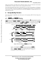
Freescale Semiconductor, Inc.
Freescale Semiconductor, Inc...
MPC107 Revision 1.3 and
1.4: Comparison and
Compatibility
Doug McQuaid
CPD Applications
risc10@email.
sps.mot.com
This document describes electrical and functional differences between Rev 1.3 and Rev 1.4 of
the MPC107 PCI Bridge/Memory Controller, which provides a bridge between the Peripheral
Component Interconnect (PCI) bus and the MPC603e, MPC740, MPC750, MPC745,
MPC755, MPC7400 and MPC7410 PowerPC™ host processors.
This document covers the following topics:
Topic
Section 1, “Overview”
Section 2, “Electrical Differences”
Section 3, “Functional Differences”
Section 4, “Compatibility Factors”
Section 5, “Conclusion”
Section 6, “Document Revision History”
1
Page
1
2
3
5
7
7
Overview
For a few years now, the production revision of the MPC107 has been Rev 1.3. However, this
version of the device is limited to a processor/memory bus frequency of 100 MHz and has
errata that some customers have deemed unsuitable for their design requirements. Recently a
new revision of the MPC107, Rev 1.4, was introduced to implement fixes for the errata to
make it more suitable for new designs. Specification changes that manufacturing supports also
addressed the frequency limitation. Because many existing designs are unaffected by the
100-MHz limit and the errata on Rev 1.3, and because Rev 1.4 introduces timing and
functional changes to the 107, many customers choose to continue specifying Rev 1.3 in their
designs. This document, which describes the differences between Rev 1.3 and Rev 1.4,
provides help to assess which revision is appropriate for a specific design and what changes
might be necessary when migrating a system design from Rev 1.3 to Rev 1.4.
© Freescale Semiconductor, Inc., 2004. All rights reserved.
For More Information On This Product,
Go to: www.freescale.com
Freescale Semiconductor, Inc.
Electrical Differences
Table 1 describes how to distinguish between Rev 1.3 and Rev 1.4 devices. The orderable part number and
the part marking contain a revision code that refers to the die mask revision number. Reading the Revision
ID register at configuration address offset 0x08 can determine the revision level of an installed device.
Table 1. Identifying Revision Level
MPC107 Die Mask Revision Level
Revision Code
Revision ID Register (offset 0x08)
1.3
C
0x13
1.4
D
0x14
Freescale Semiconductor, Inc...
Some of the MPC107 documentation is not updated to reflect the differences between Rev 1.3 and Rev 1.4
of the device. The following documents were written before the changes in Rev 1.4 of the MPC107 were
known:
•
•
MPC107 PCI Bridge/Memory Controller User’s Manual (MPC107UM/AD), Rev 0. 11/2000
Application notes
— Designing a Local Bus Slave Interface (AN1846/D), Rev 0, 3/2000
— MPC107 Design Guide (AN1849/D), Rev 0.8, 8/2000
These documents will be updated, but until their revision date surpasses the initial date of this application
note, they will not contain the information presented herein regarding Rev 1.4.
The following documents have been updated to reflect the Rev 1.4 changes:
•
•
•
2
MPC107 PCI Bridge/Memory Controller Hardware Specifications (MPC107EC/D), Rev 2,
12/2002
MPC107 Part Number Specification for the XPC107APXnnnWx Series (MPC107APXPNS/D), Rev
1, 11/2002
MPC107 PCI Bridge/Memory Controller Chip Errata (MPC107CE/D), Rev 5, 7/2002
Electrical Differences
The only changes in the electrical specifications are to allow the MPC107 to achieve 133-MHz
processor/memory bus operation timing. Note that these are specification changes that manufacturing
supports, and are not design changes. Therefore, Rev 1.4 devices marked for 100-MHz operation have the
same electrical characteristics as Rev 1.3 devices. The MPC107 Part Number Specification for the
XPC107APXnnnWx Series document describes the electrical differences for the 133-MHz-rated device in
detail. Table 2 summarizes the changes for the 133-MHz-rated Rev 1.4 MPC107.
Table 2. Electrical Differences—100 MHz/133 MHz
Rev 1.3/Rev 1.4
(100-MHz Device)
Rev 1.4
(133-MHz Device Only)
Maximum 60x and memory bus
frequency
100 MHz
133 MHz
Supply voltages—core, PLL,
and DLL
(VDD, AVDD, and LAVDD)
2.5 VDC
2.7 VDC
Electrical Characteristic
MPC107 Revision 1.3 and 1.4: Comparison and Compatibility
For More Information On This Product,
Go to: www.freescale.com
Freescale Semiconductor, Inc.
Functional Differences
Table 2. Electrical Differences—100 MHz/133 MHz (continued)
Rev 1.3/Rev 1.4
(100-MHz Device)
Rev 1.4
(133-MHz Device Only)
5.5 nsec
4.5 nsec
105 ˚C
85 ˚C
Power consumption
See MPC107 hardware specifications
Slightly higher due to elevated supply
voltage
I2C frequencies
See MPC107 hardware specifications
Higher due to higher memory bus
frequency of 133 MHz (the divisors are
the same)
Frequency range limited to 100 MHz for
PLL[0:4] configurations 0x5, 0x8, and
0xC
Frequency range higher for PLL[0:4]
configurations 0x5, 0x8, and 0xC
Electrical Characteristic
60x and memory interface
signals
—output valid time (Specs 12 b
and 12e)
Freescale Semiconductor, Inc...
Maximum die junction
temperature (Tj)
PLL[0:4] configurations
3
Functional Differences
Rev 1.3 of the MPC107 has known errata that affect functionality. Rev 1.4 fixes some of those errata, but
implementing the fixes introduced functionality changes. The following sections describe the specific Rev
1.3 errata that Rev 1.4 addressed.
3.1 Fast Back-to-Back Capability
For all revisions of the MPC107 before Rev 1.4, bit 7 of the PCI status register is hardwired to 1, indicating
the MPC107 can support fast back-to-back transactions. Due to a chip errata (#17), if an external PCI master
issues a type 2 fast back-to-back transaction (read or write) to a MPC107, the transaction causes data
corruption. (Type 2 fast back-to-back transactions access multiple targets sequentially.)
The suggested work-around for this errata is to use software to disable the ability to run fast back-to-back
transactions on any potential master devices by clearing bit 9 of the PCI command register in the master
device. The solution implemented in Revision 1.4 of the MPC107 is to hardwire bit 7 of the PCI status
register to 0, indicating that it is not capable of accepting fast back-to back transactions as a target.
3.2 MPC7450 Compatibility
Revisions of the MPC107 before Rev 1.4 have compatibility issues with the MPC7450 and its derivatives.
The compatibility issues are documented as Errata # 18 in the MPC107 chip errata. The MPC7450
implementation of the 60x bus protocol is slightly more restrictive in that data must never be transferred
before the last cycle of the ARTRY window (the cycle after AACK is asserted). Similarly, TEA must not be
asserted to terminate a data tenure before the last cycle of the ARTRY window.
The actual protocol restriction for the MPC7450 is that any transaction receiving a simultaneous AACK and
TA/TEA must not be retried. Improperly forwarded data causes data corruption in the code stream. In
addition, any transaction that requires a data tenure that follows a transaction receiving a simultaneous
MPC107 Revision 1.3 and 1.4: Comparison and Compatibility
For More Information On This Product,
Go to: www.freescale.com
Freescale Semiconductor, Inc.
Functional Differences
AACK and TA/TEA must not be retried. When the MPC7450 receives a simultaneous AACK and TA/TEA,
it sets an internal sticky flag that causes the next transaction to ignore ARTRY.
For revisions of the MPC107 before Rev 1.4, data is returned to the processor starting with the cycle when
AACK is asserted, which is one cycle before that permitted by the MPC7450. Before Rev 1.4, the MPC107
may drive DBGn (and DBGLB) as early as the cycle in which TS is asserted.
The problem is aggravated in dual-processor systems and systems where PCI accesses to memory cause
significant snoop or retry activity on the 60x bus where 60x bus traffic is high.
Beginning with Rev 1.4, the MPC107 no longer issues the first TA (or TEA) for a data tenure simultaneously
with the associated AACK for any transactions. To guarantee that TA is not asserted on or before AACK,
the timings for DBGn and DBGLB were also changed.
Freescale Semiconductor, Inc...
3.2.1 Local Bus Slave Parameters
To implement the fix for MPC7450 compatibility, two local bus slave parameters, PICR1[CF_LBA_EN]
and PICR2[CF_LBCLAIM_WS], were eliminated beginning with Rev 1.4. The CF_LBA_EN parameter
enables or disables the local bus slave functionality on revisions before Rev 1.4 whereas, starting with Rev
1.4, local bus slave functionality is always enabled.
The CF_LBCLAIM_WS parameter controls when the 107 samples the LBCLAIM input signal from the
local bus slave on revisions before 1.4. Starting with Rev 1.4 of the 107, the PICR2[CF_APHASE_WS]
parameter controls the timing of both the address phase and the sampling of LBCLAIM.
3.3 Latency for PCI Accesses to Local Memory
Due to a chip errata (#19) on revisions of the MPC107 before Rev 1.4, the processor can prevent a PCI agent
or DMA transfer from accessing the SDRAM and thereby affect the minimum PCI and/or DMA access
latency if the processor is performing a series of pipelined reads or writes. PCI and DMA accesses to local
memory may stall if snooping is disabled (PICR2[NO_SNOOP_EN] = 1) because pipelined processor
transactions have a priority 1.5 (see Table 12-2 of the MPC107 Bridge/Memory Controller User’s Manual).
The suggested work-around is to enable snooping (PICR2[NO_SNOOP_EN] = 1), even though the
hardware-managed coherency is not needed. As an additional step, in single-processor systems, the GBL
signal to the processor may be pulled down to eliminate false ARTRYs due to pipeline collisions.
Adding fairness to the internal arbitration logic that does not allow the pipelined 60x transaction to keep
winning over non-snooped PCI/DMA initiated read transactions in Rev 1.4 of the MPC107 fixed the errata.
3.4 60x Bus Grants After sync or eieio Broadcasts
Due to a chip errata (#20) on MPC107 devices before Rev 1.4, if the processor issues a sync or eieio
instruction to the MPC107, the MPC107 does not grant the 60x bus to any processor until all the internal
write buffers are empty. These buffers are the processor-to-PCI-write data buffers (PRPWB0 and
PRPWB1), the PCI-to-local-memory-write buffers (PCMWB0, and PCMWB1), and the copyback buffer.
In this case, a PCI device can perform continuous accesses into SDRAM so that the internal buffers
(PCMWB0, PCMWB1, and copyback) are never empty. In such a case, the processor is prevented from
progressing beyond the sync/eieio address broadcast.
The suggested work-around is to disable broadcasts of address-only transactions (HID0[ABE]=0) on
processors that implement the ABE bit. For systems using processors that do not implement the ABE bit
(such as the MPC7410), the work-around is much more difficult, involving external logic that decodes
MPC107 Revision 1.3 and 1.4: Comparison and Compatibility
For More Information On This Product,
Go to: www.freescale.com
Freescale Semiconductor, Inc.
Compatibility Factors
address-only broadcasts and inhibits the PCI arbitration signals to allow for transactions in the internal
PCMWBs buffers to complete to memory before resuming normal operation.
The solution implemented in Revision 1.4 of the MPC107 is to remove the dependency on flushing the
PCI-to-local-memory-write buffers (PCMWBs) after a sync/eieio broadcast before the 107 can grant the bus
to the processor. Thus, only the processor-to-PCI-write buffers (PRPWBs) are flushed before the bus is
granted to the processor.
4
Compatibility Factors
Freescale Semiconductor, Inc...
This section describes compatibility issues that may arise when migrating a MPC107-based design from
Rev 1.3 to Rev 1.4.
4.1 DBGn and DBGLB Timing
As described in Section 3.2, “MPC7450 Compatibility,” to guarantee that TA is not asserted on or before
AACK, the timings for DBGn and DBGLB were changed in Rev 1.4 to fix the MPC7450-compatibility
problem. Before Rev 1.4, the MPC107 may drive DBGn (and DBGLB) as early as the cycle in which TS is
asserted. Figure 1 shows the signal timing for DBGn and DBGLB on Rev 1.3 and Rev 1.4 devices.
60x Bus Clock
TS
AACK
60x Address
DBGn
Rev 1.3
TA
Data
DBGn
Rev 1.4
TA
Data
Single Beat
Burst
Figure 1. Rev 1.3 and Rev 1.4 DBGn Signal Timing
NOTE
For Rev 1.4 of the MPC107, DBGn is asserted coincident with AACK. If
a Rev 1.3 system design incorporates external logic that depends on the
timing of DBGn or DBGLB, the external logic must be modified to
accommodate the altered timing of Rev 1.4.
MPC107 Revision 1.3 and 1.4: Comparison and Compatibility
For More Information On This Product,
Go to: www.freescale.com
Freescale Semiconductor, Inc.
Compatibility Factors
4.2 Local Bus Slave Compatibility
As described in Section 3.2.1, “Local Bus Slave Parameters,” an impact occurs on local bus slave
functionality when moving from Rev 1.3 to Rev 1.4. Two local bus slave parameters, PICR1[CF_LBA_EN]
and PICR2[CF_LBCLAIM_WS] were eliminated
Freescale Semiconductor, Inc...
Even though the CF_LBA_EN parameter was eliminated in Rev 1.4, initialization software that sets this bit
to enable the local bus slave functionality do not cause any errors. Software that clears CF_LBA_EN to
disable the local bus slave functionality does not cause any errors; however, the functionality is always
enabled in Rev 1.4 and the clearing of this bit is ignored. A Rev 1.3 design has no reason to rely on disabling
the local bus slave functionality, and thus software should not be impacted.
The elimination of the CF_LBCLAIM_WS parameter in Rev 1.4 may affect initialization software. Starting
with Rev 1.4 of the MPC107, the PICR2[CF_APHASE_WS] parameter controls the timing of both the
address phase and the sampling of LBCLAIM. Software that attempts to program CF_LBCLAIM_WS does
not cause any errors on Rev 1.4, but the LBCLAIM sampling logic ignores the parameter. Consider this
situation to assert LBCLAIM in the appropriate cycle.
Many customers use equal settings for CF_APHASE_WS and CF_LBCLAIM_WS, and the change does
not affect them. However, if the initialization code is setting CF_APHASE_WS greater than
CF_LBCLAIM_WS and a local bus slave asserts LBCLAIM before CF_APHASE_WS expires, a Rev 1.4
MPC107 does not recognize the assertion of LBCLAIM and asserts the appropriate number of TAs for the
transaction. Typically in this situation, the system eventually hangs. The work-around is to adjust
CF_APHASE_WS for a shorter duration to accommodate the assertion of LBCLAIM or to modify the local
bus slave to delay the assertion of LBCLAIM until CF_APHASE_WS expires.
4.3 Migrating from 100 MHz to 133 MHz
If the purpose of migrating to Rev 1.4 is to increase the processor/memory bus frequency from 100 MHz to
133 MHz, the system design must account for the electrical differences that Table 2 describes. Note that not
all Rev 1.4 devices are rated for 133-MHz operation. In 133-MHz systems, use only those devices that are
specifically rated for 133-MHz operation.
Most, but not necessarily all, system designs should be re-laid out to operate properly at 133 MHz. Because
the 133-MHz Rev 1.4 MPC107 requires 2.7 VDC supply voltages for the core, PLL, and DLL, the power
supply of an existing Rev 1.3 design should be augmented to support the additional increased supply
voltage. Follow the recommendations in the MPC107 Hardware Specifications and in the MPC107 design
guide application note (AN1849/D) concerning memory timing. In general, for best signal integrity, keep
trace lengths for SDRAM signals as short as possible and keep capacitive loads to a minimum (or use
registered DIMMs that buffer the memory control signals).
MPC107 Revision 1.3 and 1.4: Comparison and Compatibility
For More Information On This Product,
Go to: www.freescale.com
Freescale Semiconductor, Inc.
Conclusion
5
Conclusion
Table 3 provides a summary of which revision of the MPC107 is appropriate for specific design
requirements. For designs that do not depend on the listed requirements, either revision provides the
functionality described in the MPC107 user’s manual.
Table 3. Which Revision To Use?
Design Requirement
MPC107 Rev 1.3
MPC107 Rev 1.4
Not suitable
Suitable (with
133 MHz-rated part)
May not be suitable
(Errata #17)
Suitable, but fast
back-to-back transactions
to the 107 are still not
supported. See
Section 3.1, “Fast
Back-to-Back Capability,”
for more information.
Not-suitable
(Errata #18)
Suitable
Local bus slave device
Suitable
Existing logic/initialization
software may need
modification. See
Section 4.2, “Local Bus
Slave Compatibility,” for
more information.
External logic that relies on DBGn or DBGLB timing
Suitable
Existing logic may need
modification. See
Section 4.1, “DBGn and
DBGLB Timing,” for more
information.
Snooping of PCI-to-local memory transactions disabled
(PICR2[NO_SNOOP_EN] = 1)
May not be suitable
(Errata #19)
Suitable
MPC7400/MPC7410 processor
May not be suitable
(Errata #20)
Suitable
133-MHz processor/memory bus
Freescale Semiconductor, Inc...
External PCI masters that may run Type 2 fast-back-to-back
transactions
MPC7450 family processor
6
Document Revision History
Table 4 details revisions and changes to this application note.
Table 4. Document Revisions
Rev. No.
Substantive Changes
0.0
Initial release
0.1
Nontechnical reformatting
MPC107 Revision 1.3 and 1.4: Comparison and Compatibility
For More Information On This Product,
Go to: www.freescale.com
Freescale Semiconductor, Inc.
How to Reach Us:
Home Page:
www.freescale.com
Freescale Semiconductor, Inc...
E-mail:
[email protected]
USA/Europe or Locations Not Listed:
Freescale Semiconductor
Technical Information Center, CH370
1300 N. Alma School Road
Chandler, Arizona 85224
+1-800-521-6274 or +1-480-768-2130
[email protected]
Europe, Middle East, and Africa:
Freescale Halbleiter Deutschland GmbH
Technical Information Center
Schatzbogen 7
81829 Muenchen, Germany
+44 1296 380 456 (English)
+46 8 52200080 (English)
+49 89 92103 559 (German)
+33 1 69 35 48 48 (French)
[email protected]
Japan:
Freescale Semiconductor Japan Ltd.
Headquarters
ARCO Tower 15F
1-8-1, Shimo-Meguro, Meguro-ku,
Tokyo 153-0064
Japan
0120 191014 or +81 3 5437 9125
[email protected]
Asia/Pacific:
Freescale Semiconductor Hong Kong Ltd.
Technical Information Center
2 Dai King Street
Tai Po Industrial Estate
Tai Po, N.T., Hong Kong
+800 2666 8080
[email protected]
For Literature Requests Only:
Freescale Semiconductor Literature Distribution Center
P.O. Box 5405
Denver, Colorado 80217
1-800-441-2447 or 303-675-2140
Fax: 303-675-2150
[email protected]
Information in this document is provided solely to enable system and software
implementers to use Freescale Semiconductor products. There are no express or
implied copyright licenses granted hereunder to design or fabricate any integrated
circuits or integrated circuits based on the information in this document.
Freescale Semiconductor reserves the right to make changes without further notice to
any products herein. Freescale Semiconductor makes no warranty, representation or
guarantee regarding the suitability of its products for any particular purpose, nor does
Freescale Semiconductor assume any liability arising out of the application or use of
any product or circuit, and specifically disclaims any and all liability, including without
limitation consequential or incidental damages. “Typical” parameters which may be
provided in Freescale Semiconductor data sheets and/or specifications can and do
vary in different applications and actual performance may vary over time. All operating
parameters, including “Typicals” must be validated for each customer application by
customer’s technical experts. Freescale Semiconductor does not convey any license
under its patent rights nor the rights of others. Freescale Semiconductor products are
not designed, intended, or authorized for use as components in systems intended for
surgical implant into the body, or other applications intended to support or sustain life,
or for any other application in which the failure of the Freescale Semiconductor product
could create a situation where personal injury or death may occur. Should Buyer
purchase or use Freescale Semiconductor products for any such unintended or
unauthorized application, Buyer shall indemnify and hold Freescale Semiconductor
and its officers, employees, subsidiaries, affiliates, and distributors harmless against all
claims, costs, damages, and expenses, and reasonable attorney fees arising out of,
directly or indirectly, any claim of personal injury or death associated with such
unintended or unauthorized use, even if such claim alleges that Freescale
Semiconductor was negligent regarding the design or manufacture of the part.
AN2455 Rev 0.1
For More Information On This Product,
Go to: www.freescale.com