1
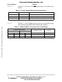
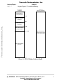
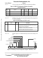
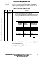
Freescale Semiconductor, Inc.
Order Number: MPC107UMAD/D
Rev. 0, 2/2001
Semiconductor Products Sector
Freescale Semiconductor, Inc...
™
Errata to
MPC107 PCI Bridge/Memory Controller User’s Manual,
rev. 0
This errata describes corrections to the MPC107 PCI Bridge/Memory Controller User’s
Manual, rev 0. For convenience, the section number and page number of the errata item in
the user’s manual are provided.
To locate any published updates for this document, refer to the world-wide web at http://
www.mot.com/powerpc.
© Motorola, Inc., 2001. All rights reserved.
For More Information On This Product,
Go to: www.freescale.com
Freescale Semiconductor, Inc.
Section #/Page #
2.1.2, 2-7
Changes
In Table 2–2, the state of the INT signal during reset should read as
follows:
Table 2–2. Output Signal States During System Reset
Interface
State During System Reset
—
—
—
EPIC control
INT
Driven (unknown until HRESET is negated), then negated.
—
—
—
3.1, 3–2
Freescale Semiconductor, Inc...
Signal
In Table 3–1, the PCI address range for the processor address range
8000_0000 through FDFF–FFFF should read as follows:
Table 3–1. Address Map B—Processor View in Host Mode
Processor Address Range
PCI Address Range
Hex
2
Definition
Decimal
—
—
—
—
—
—
8000_0000
FDFF_FFFF
2G
4G - 32M - 1
8000_0000–FDFF_FFFF
PCI memory space3
—
—
—
—
—
—
MPC107 PCI Bridge/Memory Controller User’s Manual, rev. 0
For More Information On This Product,
Go to: www.freescale.com
Freescale Semiconductor, Inc.
Section #/Page #
3.1, 3–7
Changes
Replace Figure 3–3 with the following:
MPC107
Memory Controller
PCI Master
I/O Space
0
Addressable by
local processor
64KB
Not addressable by
processor
8MB
Freescale Semiconductor, Inc...
Addressable by
processor
12MB
Not addressable by
local processor
1GB - 8MB
MPC107 does not
respond as a target
to PCI I/O accesses
Not addressable by
processor
4GB
Figure 3-3. PCI I/O Master Address Map B
MPC107 PCI Bridge/Memory Controller User’s Manual, rev. 0
For More Information On This Product,
Go to: www.freescale.com
3
Freescale Semiconductor, Inc.
Section #/Page #
Changes
4.1, 4–7
The reset value for the MCCR4 register should read as follows:
Table 4–2. MPC107 Configuration Registers Accessible
from the Processor
Address
Offset
—
0xFC
Freescale Semiconductor, Inc...
—
Register
Size
Program
Access
Size (Bytes)
Access
Reset Value
—
—
—
—
MCCR4
4 bytes
1, 2, or 4
Read/Write 0x0010_0000
—
—
—
—
4.7, 4–33
—
—
In Table 4–28, replace the name and description of the setting for bit
29 with the following:
Table 4–28. Bit Settings for PICR2—0xAC
Bits
29
Reset
Value
Name
SERIALIZE_ON_CFG
0
Description
This bit controls whether the MPC107 serializes configuration writes
to PCI devices from the processor. Note that the sense of this bit is
the opposite of that on the MPC8240.
0 Configuration writes to PCI devices from the processor do not cause
serialization. The internal buffers are not flushed.
1 Configuration writes to PCI devices from the processor cause the
MPC107 to serialize and flush the internal buffers.
4.10, 4–47
Replace Figure 4–30 with the following. Note the name change to bit
18.
EDO
ECC_EN
INLINE_RD_EN
REFINT
INLINE_WR_EN
INLINE_PAR_NOT_ECC
RSV_PG
ASFALL[0–3]
ASRISE[0–3]
RMW_
PAR
TS_WAIT_TIMER[0–2]
31 30 29 28
25 24
21 20 19 18 17 16 15
2
1
Figure 4–30. Memory Control Configuration Register 2 (MCCR2)—0xF4
4
MPC107 PCI Bridge/Memory Controller User’s Manual, rev. 0
For More Information On This Product,
Go to: www.freescale.com
0
Freescale Semiconductor, Inc.
Section #/Page #
4.10, 4–48
Changes
In Table 4-40, replace the “Wait States for ROM High Impedance”
table in the description for bits 31–29 with the following. Note the
addition of rows for 011 and 110.
Table4–40. Bit Settings for MCCR2–0xF4
Bits
TS_WAIT_
TIMER[0–2]
Freescale Semiconductor, Inc...
31–29
Name
Reset
Value
000
Description
Transaction start wait states timer. The minimum time allowed for ROM/Flash/Port
X devices to enter high impedance is 2 memory system clocks.
TS_WAIT_TIMER[0–2] adds wait states before the subsequent transaction starts in
order to account for longer disable times of a ROM/Flash/Port X device. This delay
is enforced after all ROM and Flash accesses, delaying the next memory access
from starting (for example, DRAM after ROM access, SDRAM after Flash access,
ROM after Flash access).
Note that this parameter is supported for SDRAM systems only. For EDO/FPM
DRAM systems, TS_WAIT_TIMER[0–2] must = 000.
Bits
Wait States for ROM High Impedance
Reads with
wide data path
(32 or 64-bit)
Reads with gather
data path in
flow-through or
registered buffer
mode (8, 16, 32-bit)
All writes1, 2 and reads
with gather data path
in in-line buffer mode
(8, 16, 32,-bit)
000
2 clocks
5 clocks
6 clocks
001
2 clocks
5 clocks
6 clocks
010
3 clocks
5 clocks
6 clocks
011
4 clocks
5 clocks
6 clocks
100
5 clocks
6 clocks
7 clocks
101
6 clocks
7 clocks
8 clocks
110
7 clocks
7 clocks
7 clocks
111
8 clocks
9 clocks
10 clocks
Note 1. In this context, Flash writes are defined as any write to RCS0 or
RCS1.
Note 2: For Flash writes, add the write recovery time, ROMNAL, to the
given wait states for ROM high-impedance time.
7.4, 7–19
In the bulleted list beneath the sentence “As a target, the MPC107
responds to a transaction with a retry due to the following,” the fourth
item should read as follows:
A configuration write to a PCI device is underway and
PICR2[SERIALIZE_ON_CFG] = 1.
MPC107 PCI Bridge/Memory Controller User’s Manual, rev. 0
For More Information On This Product,
Go to: www.freescale.com
5
Freescale Semiconductor, Inc.
Section #/Page #
Changes
8.7.2, 8–19
In Table 8–4, replace the description for bit 1 with the following:
Freescale Semiconductor, Inc...
Table 8–4. DSR Field Descriptions—Offsets 0x104, 0x204
Bits
Name
Reset
Value
—
—
—
—
1
EOSI
0
R/W
End-of-segment interrupt
Write1 clears 0 No end-of-segment condition. When this bit is set, it can only be cleared
by writing a 1 to it or by a hard reset.
1 After the block of data has finished transferring, this bit is set. If
CDAR[EOSIE] = 1, an interrupt is generated. Otherwise, no interrupt is
generated.
12.1.2.1, 12-4
R/W
Description
—
Replace the third paragraph of section 12–4 with the following
paragraph. The only change occurs in the fourth sentence.
When the processor requests data from PCI space, the data received
from PCI is stored in the PRPRB until all requested data has been
latched. The CCU does not terminate the address tenure of the internal
transaction until all requested data is latched in the PRPRB. If the PCI
target disconnects in the middle of the data transfer and an alternate
PCI master acquires the bus and initiates a local memory access, the
CCU retries the ongoing transaction with the processor so that the
incoming PCI transaction can be snooped. A PCI-initiated access to
local memory may require a snoop transaction on the 60x bus and also
a copyback. The CCU does not provide the data to the 60x bus (for the
processor to PCI read transaction) until all outstanding snoops for PCI
writes to local memory have completed.
13.3, 13–6
Replace the last sentence in the first paragraph of section 13.3 with the
following. Note the different ErrDR2 bits.
(The error detection bits are specifically bits 15, 13, and 12 in the PCI
status register, bits 7–4 and 2–0 in ErrDR1, bits 6, 3, 2, and 0 in
ErrDR2, and bits 8, 7, and 4 in the IMISR.)
B.1, B–1
Replace the final paragraph of section B–1 with the following:
In addition, the PCI bus uses a bit format where the most-significant
bit (msb) for data is AD31, while the 60x data bus use a bit format
where the msb is DH0. Thus, PCI data bit AD31 equates to the
processor’s data bits DH0 and DL0, while PCI data bit AD0 equates
to the processor’s data bits DH31 and DL31.
6
MPC107 PCI Bridge/Memory Controller User’s Manual, rev. 0
For More Information On This Product,
Go to: www.freescale.com
Freescale Semiconductor, Inc.
Section #/Page #
B.3, B–3
Changes
Replace the final paragraph on page B–3 with the following:
Freescale Semiconductor, Inc...
Note that the MSB on the 60x bus, D0, is placed on byte lane 0
(AD[7–0]) on the PCI bus. This occurs so D0 appears at address
0xnnnn_nn00 and not at address 0xnnnn_nn03 in the PCI space.
MPC107 PCI Bridge/Memory Controller User’s Manual, rev. 0
For More Information On This Product,
Go to: www.freescale.com
7
Freescale Semiconductor, Inc...
Freescale Semiconductor, Inc.
DigitalDNA is a trademark of Motorola, Inc.
The PowerPC name, the PowerPC logotype, and PowerPC 603e are trademarks of International Business Machines Corporation used by Motorola
under license from International Business Machines Corporation.
Information in this document is provided solely to enable system and software implementers to use PowerPC microprocessors. There are no express
or implied copyright licenses granted hereunder to design or fabricate PowerPC integrated circuits or integrated circuits based on the information in
this document.
Motorola reserves the right to make changes without further notice to any products herein. Motorola makes no warranty, representation or guarantee
regarding the suitability of its products for any particular purpose, nor does Motorola assume any liability arising out of the application or use of any
product or circuit, and specifically disclaims any and all liability, including without limitation consequential or incidental damages. “Typical” parameters
can and do vary in different applications. All operating parameters, including “Typicals” must be validated for each customer application by customer’s
technical experts. Motorola does not convey any license under its patent rights nor the rights of others. Motorola products are not designed, intended,
or authorized for use as components in systems intended for surgical implant into the body, or other applications intended to support or sustain life,
or for any other application in which the failure of the Motorola product could create a situation where personal injury or death may occur. Should Buyer
purchase or use Motorola products for any such unintended or unauthorized application, Buyer shall indemnify and hold Motorola and its officers,
employees, subsidiaries, affiliates, and distributors harmless against all claims, costs, damages, and expenses, and reasonable attorney fees arising
out of, directly or indirectly, any claim of personal injury or death associated with such unintended or unauthorized use, even if such claim alleges that
Motorola was negligent regarding the design or manufacture of the part.
Motorola and
are registered trademarks of Motorola, Inc. Motorola, Inc. is an Equal Opportunity/Affirmative Action Employer.
Motorola Literature Distribution Centers:
USA/EUROPE: Motorola Literature Distribution; P.O. Box 5405; Denver, Colorado 80217; Tel.: 1-800-441-2447 or 1-303-675-2140;
World Wide Web Address: http://ldc.nmd.com/
JAPAN: Nippon Motorola Ltd SPD, Strategic Planning Office 4-32-1, Nishi-Gotanda Shinagawa-ku, Tokyo 141, Japan Tel.: 81-3-5487-8488
ASIA/PACIFIC: Motorola Semiconductors H.K. Ltd Silicon Harbour Centre 2, Dai King Street Tai Po Industrial Estate Tai Po, New Territories, Hong
Kong
Technical Information: Motorola Inc. SPS Customer Support Center 1-800-521-6274; electronic mail address: [email protected].
Document Comments: FAX (512) 933-2625, Attn: RISC Applications Engineering.
World Wide Web Addresses: http://www.motorola.com/PowerPC
http://www.motorola.com/netcomm
http://www.motorola.com/Coldfire
MPC107UMAD/D
For More Information On This Product,
Go to: www.freescale.com