1
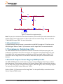
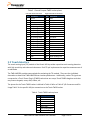
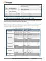
TWR-K40X256 Tower Module
User's Manual
Rev. 1.0
Freescale Semiconductor Inc.
Table of Contents
1 TWR-K40X256 and TWR-K40X256-KIT Overview ......................................................................4
1.1 Contents .................................................................................................................................................................................. 5
1.2 Features .................................................................................................................................................................................. 5
1.3 Getting Started ..................................................................................................................................................................... 7
1.4 Reference Documents ....................................................................................................................................................... 7
2 Hardware Description ...........................................................................................................................7
2.1 K40X256 Microcontroller ............................................................................................................................................... 8
2.2 Clocking .................................................................................................................................................................................. 9
2.3 System Power .................................................................................................................................................................... 10
2.3.1 RTC VBAT ........................................................................................................................................................................................... 10
2.4 Debug Interface ................................................................................................................................................................ 10
2.4.1 OSJTAG ................................................................................................................................................................................................. 10
2.4.2 Cortex Debug+ETM Connector .................................................................................................................................................. 11
2.5 Infrared Port ...................................................................................................................................................................... 11
2.6 Accelerometer ................................................................................................................................................................... 12
2.7 Potentiometer, Pushbuttons, LEDs .......................................................................................................................... 12
2.8 General Purpose Tower Plug-in (TWRPI) Socket............................................................................................... 12
2.9 Touch Interface................................................................................................................................................................. 13
2.10 Segment LCD ................................................................................................................................................................... 14
2.11 USB ...................................................................................................................................................................................... 14
2.12 Secure Digital Card Slot .............................................................................................................................................. 14
2.13 External Bus Interface – FlexBus ............................................................................................................................ 15
3 Jumper Table.......................................................................................................................................... 15
4 Input/Output Connectors and Pin Usage Table ......................................................................... 16
5 Tower Elevator Connections ............................................................................................................ 18
TWR-K40X256 Tower Module User's Manual
Page 2 of 21
List of Figures
Figure 1. Freescale Tower System Overview .............................................................................................. 4
Figure 2. Callouts on front side of the TWR-K40X256 ................................................................................ 6
Figure 3. Front side of TWR-K40X256 with TWRPI-SLCD attached............................................................. 6
Figure 4. Callouts on back side of the TWR-K40X256 ................................................................................. 7
Figure 5. TWR-K40X256 Block Diagram ...................................................................................................... 8
Figure 6. External clock source circuitry ..................................................................................................... 9
Figure 7. Infrared Port Implementation ................................................................................................... 12
Figure 8. Flexbus Connections for External Memory Port Sizes (CSCRn[BLS] = 1) ................................... 15
List of Tables
Table 1. MCG oscillator input selection resistor settings ......................................................................... 10
Table 2. Cortex Debug+ETM Connector Pinout ........................................................................................ 11
Table 3. General Purpose TWRPI socket pinout ....................................................................................... 13
Table 4. Touch TWRPI socket pinout ........................................................................................................ 13
Table 5. TWR-K40X256 Jumper Table ....................................................................................................... 15
Table 6. I/O Connectors and Pin Usage Table........................................................................................... 16
Table 7. TWR-K40X256 Primary Connector Pinout................................................................................... 18
Table 8. TWR-K40X256 Secondary Connector Pinout .............................................................................. 19
Revision History
Revision
1.0
Date
Nov 9, 2010
Changes
Initial Release for PWA 700-26547 Rev A
TWR-K40X256 Tower Module User's Manual
Page 3 of 21
1 TWR-K40X256 and TWR-K40X256-KIT Overview
The TWR-K40X256 is a Tower Controller Module compatible with the Freescale Tower System. It can
function as a stand-alone, low-cost platform for the evaluation of the Kinetis K30 and K40 family of
microcontroller (MCU) devices. The TWRPI-SLCD segment LCD daughter card is included as part of the
TWR-K40X256.
The TWR-K40X256 features the Kinetis K40 low-power microcontroller based on the ARM® Cortex™M4 architecture with USB 2.0 full-speed OTG and segment LCD display controllers. The K40X256
includes 256Kbytes of program flash storage and an additional 256Kbytes of FlexMemory non-volatile
storage that can be used as additional program flash memory, data flash, or variable size/endurance
EEPROM.
The TWR-K40X256 is available as a stand-alone product or as a kit (TWR-K40X256-KIT) with the Tower
Elevator Modules (TWR-ELEV) and the Tower Serial Module (TWR-SER). The TWR-K40X256 can also be
combined with other Freescale Tower peripheral modules to create development platforms for a wide
variety of applications. Figure 1 provides an overview of the Freescale Tower System.
Figure 1. Freescale Tower System Overview
TWR-K40X256 Tower Module User's Manual
Page 4 of 21
1.1 Contents
The TWR-K40X256 contents include:
TWR-K40X256 board assembly
Segment LCD Tower Plug-in module, TWRPI-SLCD
3ft USB cable
Interactive DVD with software installers and documentation
Quick Start Guide
The TWR-K40X256-KIT contains:
TWR-K40X256 MCU module
TWR-ELEV – Primary and Secondary Elevator Modules
TWR-SER – Serial module including USB host/device/OTG, Ethernet, CAN, RS232 and RS485
1.2 Features
Figure 2, Figure 3 and Figure 4 show the TWR-K40X256 with some of the key features called out. The
following list summarizes the features of the TWR-K40X256 Tower MCU Module:
Tower compatible microcontroller module
MK40X256VMD100: K40X256 in a 144 MAPBGA with 100MHz operation
Touch and Segment LCD Tower Plug-in Socket
Segment LCD Tower Plug-in module, TWRPI-SLCD
General purpose Tower Plug-in (TWRPI) socket
On-board JTAG debug circuit (OSJTAG) with virtual serial port
Three axis accelerometer (MMA7660)
Four (4) user-controllable LEDs
Four (4) capacitive touch pads
Two (2) user pushbutton switches
Potentiometer
Battery Holder for 20mm lithium battery (e.g. 2032, 2025)
SD Card slot
TWR-K40X256 Tower Module User's Manual
Page 5 of 21
Figure 2. Callouts on front side of the TWR-K40X256
Figure 3. Front side of TWR-K40X256 with TWRPI-SLCD attached
TWR-K40X256 Tower Module User's Manual
Page 6 of 21
Figure 4. Callouts on back side of the TWR-K40X256
1.3 Getting Started
Follow the Quick Start Guide found printed in the TWR-K40X256 box or the interactive DVD for the list
of recommended steps for getting started. There are also lab walk-through guides available on the
tool support page for the TWR-K40X256: http://www.freescale.com/TWR-K40X256.
1.4 Reference Documents
The documents listed below should be referenced for more information on the Kinetis family, Tower
System, and MCU Modules. These can be found in the documentation section of freescale.com/TWRK40X256 or freescale.com/kinetis.
TWR-K40X256-QSG: Quick Start Guide
TWR-K40X256-SCH: Schematics
TWR-K40X256-PWA: Design Package
TWRPI-SLCD-SCH: Schematics
TWRPI-SLCD-PWA: Design Package
K40 Family Product Brief
K40 Family Reference Manual
Kinetis Quick Reference User Guide (QRUG)
Tower Configuration Tool
2 Hardware Description
The TWR-K40X256 is a Tower Controller Module featuring the MK40X256VMD100—an ARM CortexM4 based microcontroller with segment LCD and USB 2.0 full-speed OTG controllers in a 144 MAPBGA
package with a maximum core operating frequency of 100MHz. It is intended for use in the Freescale
Tower System but can operate stand-alone. An on-board debug circuit, OSJTAG, provides a JTAG
debug interface and a power supply input through a single USB mini-AB connector. Figure 5 shows a
block diagram of the TWR-K40X256. The following sections describe the hardware in more detail.
TWR-K40X256 Tower Module User's Manual
Page 7 of 21
Tower Elevator Expansion Connectors
SDHC, I2S, SPI, I2C, ADC, USB, DAC, PWM, UARTs, Flexbus, Segment LCD
5.0V
8 MHz XTAL
32.768 KHz XTAL
IR Output
Comparator
5.0V
USB
Mini-B
OSJTAG
JTAG, Power, SCI
K40X256
144 MAPBGA
GPIO / Interrupts
VBAT (RTC)
ADC
TSI, GPIO
I2C
SPI, I C, ADC, GPIO
General Purpose
Tower Plug-in
(TWRPI)
Freescale Device
LED
LED
2
SD Card Slot
LED
LED
Reset
SDHC
Infrared Port
JTAG
SCI
Battery
Holder
3.3V
Touch & Segment LCD
Tower Plug-in (TWRPI)
MMA7660
External Connectors
Interface Circuits
Capacitive
Touch
Pads
Power
Figure 5. TWR-K40X256 Block Diagram
2.1 K40X256 Microcontroller
The TWR-K40X256 module features the MK40X256VMD100. The K40 microcontroller family is part of
the Kinetis portfolio of devices built around an ARM Cortex-M4 core. Refer to the K40 Family Product
Brief and the K40 Family Reference Manual for comprehensive information on the MK40X256VMD100
device. The key features are listed here:
32-bit ARM Cortex-M4 core with DSP instructions
100MHz maximum core operating frequency
144 MAPBGA, 13mm x 13mm, 1.0mm pitch package
1.71V – 3.6V operating voltage input range
256 Kbytes of program flash, 64 Kbytes of static RAM
FlexMemory consisting of 256 Kbytes of FlexNVM (non-volatile flash memory that can be used
as program flash, data flash, backup EEPROM of variable endurance and size) and 4 Kbytes of
FlexRAM (RAM memory that can be used as traditional RAM, as high-endurance EEPROM
storage, or flash programming acceleration RAM)
External bus interface
Power management controller with 10 different power modes
Multi-purpose clock generator with PLL and FLL operation modes
16-bit SAR ADC, 12-bit DAC
High-speed analog comparator with 6-bit DAC
Programmable voltage reference
TWR-K40X256 Tower Module User's Manual
Page 8 of 21
USB full-speed/low-speed OTG/Host/Device controller with device charge detect
SPI, I2C (w/ SMBUS support), UART (w/ ISO7816 and IrDA), CAN, I2S
SD Host Controller (SDHC)
GPIO with pin interrupt support, DMA request capability, digital glitch filtering
Capacitive touch sensing inputs (TSI)
LCD display driver supporting 3V and 5V glass, configurable frontplane and backplane pins, and
segment failure detection
Debug interfaces: JTAG, cJTAG, SWD
Trace: TPIO, FPB, DWT, ITM, ETM, ETB
2.2 Clocking
The Kinetis MCUs start up from an internal digitally controlled oscillator (DCO). Software can enable
one or two external oscillators if desired. The external oscillator for the Multipurpose Clock Generator
(MCG) module can range from 32.768 KHz up to a 32 MHz crystal or ceramic resonator. The external
oscillator for the Real Time Clock (RTC) module accepts a 32.768 kHz crystal.
DNP
32KHz_XTL
18PF
1
C31
Y3
32.768KHz
R93
R94
1.0M
R91
DNP
C37
2
DNP
32KHz_EXTL
18PF
XTAL32_RTC
0
0
DNP
R95
EXTAL32_RTC
0
R97
0
DNP
DNP
0
0
R87
R88
R81
DNP
0
DNP
R89
0
8MHz_XTL_R
R86
0
XTAL_MAIN
8MHz_EXTL
R83
0
EXTAL_MAIN
CLKIN0
R84
0
1
8MHz_XTL
X3
8.00MHZ
3
2
8
R85
1.0M
DNP
Figure 6. External clock source circuitry
The clocking circuitry on the TWR-K40X256 is shown on sheet 4 of the schematics and in Figure 6. An
8.0 MHz ceramic resonator with built-in load capacitors is the default external source for the MCG
oscillator inputs (XTAL/EXTAL_MAIN). A 32.768 KHz crystal is connected to the RTC oscillator inputs by
default. There are optional resistors (not populated by default) to allow for the MCG oscillator inputs
to be routed from any one of the 8.0 MHz resonator, the 32.678 KHz crystal, or the clock input pin
CLKIN0 from the Primary Connector (pin B24). Table 1 shows the resistor settings for each of the MCG
oscillator input options.
TWR-K40X256 Tower Module User's Manual
Page 9 of 21
Table 1. MCG oscillator input selection resistor settings
MCG Oscillator Input
R93 R91 R95 R97 R81 R88 R87 R86 R83 R84
X
―
X
―
―
―
―
X
X
―
8.0 MHz Resonator
―
X
―
X
X
X
―
―
―
―
32.768 KHz RTC Crystal
X
―
X
―
―
―
X
―
―
X
Clock Input from CLKIN0
"X" indicates that the resistor is installed; "―" indicates that the resistor is not
populated. All resistor values are 0 ohm.
2.3 System Power
In stand-alone operation, the power source for the TWR-K40X256 module is derived from the 5.0V
input from either the USB mini-B connector, J16, or the debug header, J14, when a shunt is placed on
jumper J15. A low-dropout regulator provides a 3.3V supply from the 5.0V input voltage. Refer to
sheet 5 of the TWR-K40X256 schematics for more details.
When installed into a Tower System, the TWR-K40X256 can be powered from either an on-board
source or from another source in the assembled Tower System. If both the on-board and off-board
sources are available, the TWR-K40X256 will default to the off-board source.
The 3.3V power supplied to the MCU is routed through a jumper, J11. The jumper shunt can be
removed to allow for either 1) alternate MCU supply voltages to be injected or 2) the measurement of
power consumed by the MCU.
2.3.1 RTC VBAT
The Real Time Clock (RTC) module on the K40 has two modes of operation, system power-up and
system power-down. During system power-down, the RTC is powered from the backup power supply,
VBAT. The TWR-K40X256 provides a battery holder for a coin cell battery that can be used as the VBAT
supply. The holder can accept common 20mm diameter 3V lithium coin cell batteries (e.g. 2032,
2025). Refer to the description J12 in Table 5 “TWR-K40X256 Jumper Table” for more information.
2.4 Debug Interface
There are two debug interface options provided: the on-board OSJTAG circuit and an external Cortex
Debug+ETM connector.
2.4.1 OSJTAG
An on-board MC9S08JM60 based Open Source JTAG (OSJTAG) circuit provides a JTAG debug interface
to the K40X256. A standard USB A male to Mini-B male cable (provided) can be used for debugging via
the USB connector, J16. The OSJTAG interface also provides a USB to serial bridge. Drivers for the
OSJTAG interface are provided in the P&E Micro Kinetis Tower Toolkit (available on the included DVD).
Note: The port pins connected to the OSJTAG USB-to-serial bridge (PTD6 and PTD7) are also connected
to the infrared interface. Refer to Table 6 “I/O Connectors and Pin Usage Table” and Table 5 “TWRK40X256 Jumper Table” for more information.
TWR-K40X256 Tower Module User's Manual
Page 10 of 21
2.4.2 Cortex Debug+ETM Connector
The Cortex Debug+ETM connector is a 20-pin (0.05") connector providing access to the SWD, SWV,
JTAG, cJTAG, EzPort and ETM trace (4-bit) signals available on the K40 device. The pinout and K40 pin
connections to the debug connector, J14, is shown in Table 2Table 2.
Table 2. Cortex Debug+ETM Connector Pinout
Pin
1
2
3
4
5
6
7
8
9
10
11
12
13
14
15
16
17
18
19
20
Function
VTref
TMS / SWDIO
GND
TCK / SWCLK
GND
TDO / SWO
Key
TDI
GNDDetect
nRESET
Target Power
TRACECLK
Target Power
TRACEDATA[0]
GND
TRACEDATA[1]
GND
TRACEDATA[2]
GND
TRACEDATA[3]
TWR-K40X256 Connection
3.3V MCU supply (P3V3_MCU)
PTA3/SCI0_RTS_b/FTM0_CH0/JTAG_MS/SWD_DIO
GND
PTA0/SCI0_CTS_b/FTM0_CH5/JTAG_CLK/SWD_CLK/EZP_CLK
GND
PTA2/SCI0_TX/FTM0_CH7/JTAG_DO/TRACE_SWO/EZP_DO
―
PTA1/SCI0_RX/FTM0_CH6/JTAG_DI/EZP_DI
PTA4/FTM0_CH1/MS/NMI_b/EZP_CS_b
RESET_b
5V supply (via J15)
PTA6/FTM0_CH3/FB_CLKOUT/TRACE_CLKOUT
5V supply (via J15)
PTA10/FTM2_CH0/FB_AD15/FTM2_QD_PHA/TRACE_D0
GND
PTA9/FTM1_CH1/FB_AD16/FTM1_QD_PHB/TRACE_D1
GND
PTA8/FTM1_CH0/FB_AD17/FTM1_QD_PHA/TRACE_D2
GND
PTA7/FTM0_CH4/FB_AD18/TRACE_D3
Note: Many of the trace signals connected to the debug connector are also connected elsewhere on
the TWR-K40X256. Refer to Table 6 “I/O Connectors and Pin Usage Table” and Table 7 “TWR-K40X256
Primary Connector Pinout” for more information.
2.5 Infrared Port
An infrared transmit and receive interface is implemented as shown in Figure 7 below. The CMT_IRO
pin directly drives an infrared diode. The receiver uses an infrared phototransistor connected to an onchip analog comparator through a low-pass filter. Internal to the K40 device, the output of the analog
comparator can be routed to a UART module for easier processing of the incoming data stream.
TWR-K40X256 Tower Module User's Manual
Page 11 of 21
P3V3
R24
1.54K
R25
2
IRDA_SEN
CMP0_IN0
1.0K
Q3
QTLP610CPD
C5
0.1UF
CMT_IRO
2
1
1
PTD7
PTC6
IRDAJ
2
D3
R23
1
IRDAR
QTLP610CIR
J6
33
HDR 1X2 TH
Default: no shunt
(Disable IRDA)
Figure 7. Infrared Port Implementation
Note: The port pins connected to the infrared interface (PTD6 and PTD7) are also connected to the
OSJTAG USB-to-serial bridge. Refer to Table 6 “I/O Connectors and Pin Usage Table” and Table 5
“TWR-K40X256 Jumper Table” for more information.
2.6 Accelerometer
An MMA7660 digital accelerometer is connected to the K40 MCU through an I2C interface and a
GPIO/IRQ signal. Refer to Table 6 “I/O Connectors and Pin Usage Table” for connection details.
2.7 Potentiometer, Pushbuttons, LEDs
The TWR-K40X256 features two pushbutton switches connected to GPIO/interrupt signals, one
pushbutton connected to the master reset signal, four capacitive touch pad electrodes, four usercontrollable LEDs, and a potentiometer connected to an ADC input signal. Refer to Table 6 “I/O
Connectors and Pin Usage Table” for information about which port pins are connected to these
features.
2.8 General Purpose Tower Plug-in (TWRPI) Socket
The TWR-K40X256 features a socket that can accept a variety of different Tower Plug-in modules
featuring sensors, RF transceivers, and more. The General Purpose TWRPI socket provides access to
I2C, SPI, IRQs, GPIOs, timers, analog conversion signals, TWRPI ID signals, reset, and voltage supplies.
The pinout for the TWRPI Socket is defined in Table 3.
Refer to Table 6 “I/O Connectors and Pin Usage Table” for the specific K40 pin connections to the
General Purpose TWRPI socket.
TWR-K40X256 Tower Module User's Manual
Page 12 of 21
Table 3. General Purpose TWRPI socket pinout
Left-side 2x10 Connector
Pin Description
1
5V VCC
2
3.3 V VCC
3
GND
4
3.3V VDDA
5
VSS (Analog GND)
6
VSS (Analog GND)
7
VSS (Analog GND)
8
ADC: Analog 0
9
ADC: Analog 1
10 VSS (Analog GND)
11 VSS (Analog GND)
12 ADC: Analog 2
13 VSS (Analog GND)
14 VSS (Analog GND)
15 GND
16 GND
17 ADC: TWRPI ID 0
18 ADC: TWRPI ID 1
19 GND
20 Reset
Right-side 2x10 Connector
Pin Description
1
GND
2
GND
3
I2C: SCL
4
I2C: SDA
5
GND
6
GND
7
GND
8
GND
9
SPI: MISO
10 SPI: MOSI
11 SPI: SS
12 SPI: CLK
13 GND
14 GND
15 GPIO: GPIO0/IRQ
16 GPIO: GPIO1/IRQ
17 GPIO: GPIO2
18 GPIO: GPIO3
19 GPIO: GPIO4/Timer
20 GPIO: GPIO5/Timer
2.9 Touch Interface
The touch sensing input (TSI) module of the Kinetis MCUs provides capacitive touch sensing detection
with high sensitivity and enhanced robustness. Each TSI pin implements the capacitive measurement of
an electrode.
The TWR-K40X256 provides two methods for evaluating the TSI module. There are four individual
electrodes on-board the TWR-K40X256 that simulate pushbuttons. Additionally, twelve TSI signals are
connected to a Touch Tower Plug-in (TWRPI) socket that can accept Touch TWRPI daughter cards that
may feature keypads, rotary dials, sliders, etc.
The pinout for the Touch TWRPI socket is defined in Table 4. Refer to Table 6 “I/O Connectors and Pin
Usage Table” for the specific K40 pin connections to the Touch TWRPI socket.
Table 4. Touch TWRPI socket pinout
Pin
1
2
3
4
5
6
7
Description
5V VCC
3.3 V VCC
Electrode 0
3.3V VDDA
Electrode 1
VSS (Analog GND)
Electrode 2
TWR-K40X256 Tower Module User's Manual
Page 13 of 21
Pin
8
9
10
11
12
13
14
15
16
17
18
19
20
Description
Electrode 3
Electrode 4
Electrode 5
Electrode 6
Electrode 7
Electrode 8
Electrode 9
Electrode 10
Electrode 11
ADC: TWRPI ID 0
ADC: TWRPI ID 1
GND
Reset
2.10 Segment LCD
The segment LCD signals on the K40 devices are multiplexed with many other interface signals
including several TSI signals that are accessible on the Touch TWRPI socket. Therefore, the Touch
TWRPI socket on the TWR-K40X256 may also be used to evaluate the segment LCD controller of the
K40 device. The TWRPI-SLCD daughter card included with the TWR-K40X256 plugs into the Touch
TWRPI socket and provides a 28-segment LCD that can be driven directly by the K40 MCU. Refer to
Table 6 “I/O Connectors and Pin Usage Table” for the segment LCD signals connection details.
Additionally, many more segment LCD signals are routed to the Secondary Connector on the TWRK40X256 and can be accessed from another Tower module or on the expansion connectors of the
Secondary Elevator. Refer to Table 8 “TWR-K40X256 Secondary Connector Pinout” for connection
details.
2.11 USB
The K40X256 features a USB full-speed/low-speed OTG/Host/Device controller with built-in
transceiver. The TWR-K40X256 routes the USB D+ and D- signals from the K40 MCU to the Primary
Connector, allowing the connection to USB connectors or additional circuitry on a Tower peripheral
module.
The TWR-SER module included as part of the TWR-K40X256-KIT provides a USB OTG/Host/Device
interface with a mini-AB USB connector. There are many configuration options that can be selected to
evaluate different USB modes of operation. By default, the TWR-SER is configured for USB Device
operation. Please refer to the documentation included with the TWR-SER for more information on the
configuration options.
2.12 Secure Digital Card Slot
A Secure Digital (SD) card slot is available on the TWR-K40X256 connected to the SD Host Controller
(SDHC) signals of the K40 MCU. This slot will accept SD memory cards as well as Secure Digital Input
Output (SDIO) cards. Refer to Table 6 “I/O Connectors and Pin Usage Table” for the SDHC signal
connection details.
TWR-K40X256 Tower Module User's Manual
Page 14 of 21
2.13 External Bus Interface – FlexBus
The K40 device features a multi-function external bus interface called the FlexBus interface controller
capable of interfacing to slave-only devices. The FlexBus interface is not used directly on the TWRK40X256. Instead, a subset of the FlexBus is connected to the Primary Connector so that the external
bus can access devices on Tower peripheral modules.
The Primary Connector supports up to 20 address lines, 8 data lines, 2 chip-selects, read/write, and
output enable signals. The SDHC signals of the K40 are multiplexed over the upper FlexBus address
signals (FB_AD[27:23]), so a multiplexed mode of operation is used on the TWR-K40X256. An address
latch is provided to de-multiplex the address and data signals prior to connecting them to the Primary
Connector. Refer to sheet 8 of the TWR-K40X256 schematics for more details.
Note: The K40 Flexbus implementation provides an option for byte lane alignment. On the TWRK40X256, FB_AD[7:0] are used for the data byte. Therefore, for proper operation software must set the
CSCRx[BLS] bit to shift the data bus to the right byte lane. Refer to the FlexBus chapter in the K40
Family Reference Manual for more information.
Figure 8. Flexbus Connections for External Memory Port Sizes (CSCRn[BLS] = 1)
3 Jumper Table
There are several jumpers on the TWR-K40X256 that provide configuration selection and signal
isolation. Refer to the following table for details. The default installed jumper settings are shown in
bold with asterisks.
Table 5. TWR-K40X256 Jumper Table
Jumper
Option
Setting
*ON*
Description
Connect USB0_VBUS from Primary Elevator (A57) to VREGIN
J3
USB VREGIN Power
Connection
J5
Flexbus Address Latch
Selection
J6
Infrared Transmitter
Connection
*OFF*
Disconnect PTD7/CMT_IRO/UART0_TX from IR Transmitter (D3)
J11
MCU Power Connection
*ON*
Connect on-board 3.3V supply to MCU
OFF
Disconnect VREGIN from Primary Elevator
1-2
Flexbus address latch disabled
*2-3*
Flexbus address latch enabled
ON
Connect PTD7/CMT_IRO/UART0_TX to IR Transmitter (D3)
TWR-K40X256 Tower Module User's Manual
Page 15 of 21
OFF
*1-2*
J12
VBAT Power Selection
J13
OSJTAG Mode Selection
J15
JTAG Power Connection
2-3
ON
*OFF*
ON
*OFF*
Isolate MCU from power supply (allows for external supply or
power measurements)
Connect VBAT to on-board 3.3V supply
Connect VBAT to the higher voltage between on-board 3.3V
supply or coin-cell supply
OSJTAG bootloader mode (OSJTAG firmware reprogramming)
Debugger mode
Connect on-board 5V supply to JTAG port (supports powering
board from external JTAG probe)
Disconnect on-board 5V supply from JTAG port
4 Input/Output Connectors and Pin Usage Table
The following table provides details on which K40X256 pins are using to communicate with the LEDs,
switches, and other I/O interfaces onboard the TWR-K40X256.
Note: Some port pins are used in multiple interfaces on-board and many are potentially connected to
off-board resources via the Primary and Secondary Connectors. Take care to avoid attempted
simultaneous usage of mutually exclusive features.
Table 6. I/O Connectors and Pin Usage Table
Feature
OSJTAG USB-toSerial Bridge
SD Card Slot
Infrared Port
Pushbuttons
Touch Pads
LEDs
Connection
OSJTAG Bridge RX Data
OSJTAG Bridge TX Data
SD Clock
SD Command
SD Data0
SD Data1
SD Data2
SD Data3
SD Card Detect
SD Write Protect
IR Transmit
IR Receive
SW3 (IRQ0)
SW4 (IRQ1)
SW5 (RESET)
E1 / Touch
E2 / Touch
E3 / Touch
E4 / Touch
E1 / Orange LED
E2 / Yellow LED
Port Pin
PTD6
PTD7
PTE2
PTE3
PTE1
PTE0
PTE5
PTE4
PTA16
PTE27
PTD7
PTC6
PTC5
PTC13
RESET_b
PTB17
PTB18
PTB19
PTB16
PTC7
PTC8
Pin Function
UART0_RX
UART0_TX
SDHC0_DCLK
SDHC0_CMD
SDHC0_D0
SDHC0_D1
SDHC0_D2
SDHC0_D3
PTA16
PTE27
CMT_IRO
CMP0_IN0
PTC5
PTC13
RESET_b
TSI0_CH10
TSI0_CH11
TSI0_CH12
TSI0_CH9
PTC7
PTC8
TWR-K40X256 Tower Module User's Manual
Page 16 of 21
Potentiometer
SSI0 Access Header
Accelerometer
General Purpose
TWRPI Socket
Touch Pad /
Segment LCD TWRPI
Socket
E3 / Green LED
E4 / Blue LED
Potentiometer (R71)
SSI Header (J4 Pin 1)
SSI Header (J4 Pin 2)
SSI Header (J4 Pin 3)
SSI Header (J4 Pin 4)
SSI Header (J4 Pin 5)
SSI Header (J4 Pin 6)
SSI Header (J4 Pin 7)
I2C SDA
I2C SCL
IRQ
TWRPI AN0 (J8 Pin 8)
TWRPI AN1 (J8 Pin 9)
TWRPI AN2 (J8 Pin 12)
TWRPI ID0 (J8 Pin 17)
TWRPI ID1 (J8 Pin 18)
TWRPI I2C SCL (J9 Pin 3)
TWRPI I2C SDA (J9 Pin 4)
TWRPI SPI MISO (J9 Pin 9)
TWRPI SPI MOSI (J9 Pin
10)
TWRPI SPI SS (J9 Pin 11)
TWRPI SPI CLK (J9 Pin 12)
TWRPI GPIO0 (J9 Pin 15)
TWRPI GPIO1 (J9 Pin 16)
TWRPI GPIO2 (J9 Pin 17)
TWRPI GPIO3 (J9 Pin 18)
TWRPI GPIO4 (J9 Pin 19)
Electrode 0 (J7 Pin 3)
Electrode 1 (J7 Pin 5)
Electrode 2 (J7 Pin 7)
Electrode 3 (J7 Pin 8)
Electrode 4 (J7 Pin 9)
Electrode 5 (J7 Pin 10)
Electrode 6 (J7 Pin 11)
Electrode 7 (J7 Pin 12)
Electrode 8 (J7 Pin 13)
Electrode 9 (J7 Pin 14)
Electrode 10 (J7 Pin 15)
Electrode 11 (J7 Pin 16)
TWRPI ID0 (J7 Pin 17)
PTC9
PTB11
―
PTA16
PTA13
PTA12
PTA15
PTA5
PTA14
PTA17
PTC11
PTC10
PTC12
―
―
―
―
―
PTC10
PTC11
PTB23
PTC9
PTB11
ADC1_DM1
SSI0_RX_FS
SSI0_TX_FS
SSI0_TXD
SSI0_RXD
SSI_RX_BCLK
SSI0_TX_BCLK
SSI0_MCLK/SSI0_CLKIN
I2C1_SDA
I2C1_SCL
PTC12
ADC0_DP0/ADC1_DP3
ADC0_DM0/ADC1_DM3
ADC1_DP0/ADC0_DP3
ADC0_DP1
ADC0_DM1
I2C1_SCL
I2C1_SDA
SPI2_SIN
PTB22
PTB20
PTB21
PTC12
PTB9
PTB10
PTC5
PTA5
PTB0
PTB1
PTB2
PTB3
PTC0
PTC1
PTC2
PTA4
PTB16
PTB17
PTB18
PTB19
―
SPI2_SOUT
SPI2_PCS0
SPI2_SCK
PTC12
PTB9
PTB10
PTC5
PTA5
TSI0_CH0 / LCD_P0
TSI0_CH6 / LCD_P1
TSI0_CH7 / LCD_P2
TSI0_CH8 / LCD_P3
TSI0_CH13 / LCD_P20
TSI0_CH14 / LCD_P21
TSI0_CH15 / LCD_P22
TSI0_CH5
TSI0_CH9 / LCD_P12
TSI0_CH10 / LCD_P13
TSI0_CH11 / LCD_P14
TSI0_CH12 / LCD_P15
ADC1_DP1
TWR-K40X256 Tower Module User's Manual
Page 17 of 21
TWRPI ID1 (J7 Pin 18)
―
ADC1_DM0/ADC0_DM3
5 Tower Elevator Connections
The TWR-K40X256 features two expansion card-edge connectors that interface to the Primary and
Secondary Elevator boards in a Tower system. The Primary Connector (comprised of sides A and B)
and Secondary Connector (comprised of sides C and D) are both utilized by the TWR-K40X256. Table 7
provides the pinout for the Primary Connector. Table 8 provides the pinout for the Secondary
Connector.
Table 7. TWR-K40X256 Primary Connector Pinout
Pin
#
B1
B2
B3
B4
B5
B6
B7
B8
B9
B10
B11
B12
B13
B14
B15
B16
B17
B18
B19
B20
B21
B22
B23
B24
B25
B26
B27
B28
B29
B30
B31
B32
B33
B34
B35
B36
B37
B38
B39
B40
B41
B42
B43
Side B
Name
Usage
5V
5.0V Power
GND
Ground
3.3V
3.3V Power
ELE_PS_SENSE
Elevator Power Sense
GND
Ground
GND
Ground
SDHC_CLK / SPI1_CLK
PTE2
SDHC_D3 / SPI1_CS1_b
SDHC_D3 / SPI1_CS0_b
PTE4
SDHC_CMD / SPI1_MOSI
PTE1
SDHC_D0 / SPI1_MISO
PTE3
ETH_COL
ETH_RXER
ETH_TXCLK
ETH_TXEN
ETH_TXER
ETH_TXD3
ETH_TXD2
ETH_TXD1
ETH_TXD0
GPIO1 / RTS1
GPIO2 / SDHC_D1
GPIO3
CLKIN0
CLKOUT1
GND
AN7
AN6
AN5
AN4
GND
DAC1
TMR3
TMR2
GPIO4
3.3V
PWM7
PWM6
PWM5
PWM4
CANRX0
CANTX0
1WIRE
PTC18
PTE0
PTE28
PTA18
PTE26
Ground
PTB0
PTB1
PTB2
PTB3
Ground
DAC1_OUT
PTC5
PTD6
PTB9
3.3V Power
PTA2
PTA1
PTD5
PTD4
PTE25
PTE24
Pin
#
Side A
A1
A2
A3
A4
A5
A6
A7
A8
A9
A10
A11
Name
5V
GND
3.3V
3.3V
GND
GND
SCL0
SDA0
GPIO9 / CTS1
GPIO8 / SDHC_D2
GPIO7 / SD_WP_DET
A12
A13
A14
A15
A16
A17
A18
A19
A20
A21
A22
A23
A24
A25
A26
A27
A28
A29
A30
A31
A32
A33
A34
A35
A36
A37
A38
A39
A40
A41
A42
A43
ETH_CRS
ETH_MDC
ETH_MDIO
ETH_RXCLK
ETH_RXDV
ETH_RXD3
ETH_RXD2
ETH_RXD1
ETH_RXD0
SSI_MCLK
SSI_BCLK
SSI_FS
SSI_RXD
SSI_TXD
GND
AN3
AN2
AN1
AN0
GND
DAC0
TMR1
TMR0
GPIO6
3.3V
PWM3
PWM2
PWM1
PWM0
RXD0
TXD0
RXD1
TWR-K40X256 Tower Module User's Manual
Usage
5.0V Power
Ground
3.3V Power
3.3V Power
Ground
Ground
PTC10
PTC11
PTC19
PTE5
PTE27
PTA17
PTA14
PTA13
PTA15
PTA12
Ground
PGA0_DP/ADC0_DP0/ADC1_DP3
PGA0_DM/ADC0_DM0/ADC1_DM3
PGA1_DP/ADC1_DP0/ADC0_DP3
PGA1_DM/ADC1_DM0/ADC0_DM3
Ground
DAC0_OUT
PTA9
PTA8
PTB10
3.3V Power
PTC4
PTC3
PTC2
PTC1
PTC14
PTC15
PTC16
Page 18 of 21
Pin
#
B44
B45
B46
B47
B48
B49
B50
B51
B52
B53
B54
B55
B56
B57
B58
B59
B60
B61
B62
B63
B64
B65
B66
B67
B68
B69
B70
B71
B72
B73
B74
B75
B76
B77
B78
B79
B80
B81
B82
Side B
Name
Usage
SPI0_MISO
PTD3
SPI0_MOSI
PTD2
SPI0_CS0_b
PTD0
SPI0_CS1_b
PTC3
SPI0_CLK
PTD1
GND
Ground
SCL1
PTB2
SDA1
PTB3
GPIO5 / SD_CARD_DET
PTA16
USB0_DP_PDOWN
USB0_DM_PDOWN
IRQ_H
PTB5
IRQ_G
PTB5
IRQ_F
PTB6
IRQ_E
PTB6
IRQ_D
PTB7
IRQ_C
PTB7
IRQ_B
PTB8
IRQ_A
PTB8
EBI_ALE / EBI_CS1_b
PTE6
EBI_CS0_b
PTE7
GND
Ground
PTA10
EBI_AD15
PTA9
EBI_AD16
PTA8
EBI_AD17
PTA7
EBI_AD18
EBI_AD19
PTA29
EBI_R/W_b
PTD15
EBI_OE_b
PTA11
EBI_D7
PTD12
EBI_D6
PTD13
EBI_D5
PTD14
EBI_D4
PTE8
EBI_D3
PTE9
EBI_D2
PTE10
EBI_D1
PTE11
EBI_D0
PTE12
GND
Ground
3.3V
3.3V Power
Pin
#
A44
A45
A46
A47
A48
A49
A50
A51
A52
A53
A54
A55
A56
A57
A58
A59
A60
A61
A62
A63
A64
A65
A66
A67
A68
A69
A70
A71
A72
A73
A74
A75
A76
A77
A78
A79
A80
A81
A82
Side A
Name
TXD1
VSS
VDDA
VREFA1
VREFA2
GND
GPIO14
GPIO15
GPIO16
GPIO17
USB0_DM
USB0_DP
USB0_ID
USB0_VBUS
TMR7
TMR6
TMR5
TMR4
RSTIN_b
RSTOUT_b
CLKOUT0
GND
EBI_AD14
EBI_AD13
EBI_AD12
EBI_AD11
EBI_AD10
EBI_AD9
EBI_AD8
EBI_AD7
EBI_AD6
EBI_AD5
EBI_AD4
EBI_AD3
EBI_AD2
EBI_AD1
EBI_AD0
GND
3.3V
Usage
PTC17
VSSA
VDDA
VREFH
VREFL
Ground
USB0_DM
USB0_DP
VREGIN
RESET_b
RESET_b
PTA6
Ground
PTA24
PTA25
PTA26
PTA27
PTA28
PTA29
PTD11
LATCH_FBA7
LATCH_FBA6
LATCH_FBA5
LATCH_FBA4
LATCH_FBA3
LATCH_FBA2
LATCH_FBA1
LATCH_FBA0
Ground
3.3V Power
Table 8. TWR-K40X256 Secondary Connector Pinout
Pin
#
Side D
D1
D2
D3
D4
D5
D6
D7
D8
D9
D10
D11
Name
5V
GND
3.3V
ELE_PS_SENSE
GND
GND
SPI2_CLK
SPI2_CS1_b
SPI2_CS0_b
SPI2_MOSI
SPI2_MISO
D12
D13
ETH_COL
ETH_RXER
Usage
5.0V Power
Ground
3.3V Power
Elevator Power Sense
Ground
Ground
Pin
#
Side C
C1
C2
C3
C4
C5
C6
C7
C8
C9
C10
C11
Name
5V
GND
3.3V
3.3V
GND
GND
SCL2
SDA2
GPIO25
ULPI_STOP
ULPI_CLK
C12
C13
GPIO26
ETH_MDC
TWR-K40X256 Tower Module User's Manual
Usage
5.0V Power
Ground
3.3V Power
3.3V Power
Ground
Ground
Page 19 of 21
Pin
#
D14
D15
D16
D17
D18
D19
D20
D21
D22
D23
D24
D25
D26
D27
D28
D29
D30
D31
D32
D33
D34
D35
D36
D37
D38
D39
D40
D41
D42
D43
D44
D45
D46
D47
D48
D49
D50
D51
D52
D53
D54
D55
D56
D57
D58
D59
D60
D61
D62
D63
D64
D65
D66
D67
D68
D69
D70
D71
Side D
Name
Usage
ETH_TXCLK
ETH_TXEN
GPIO18
GPIO19 / SDHC_D4
GPIO20 / SDHC_D5
ETH_TXD1
ETH_TXD0
ULPI_NEXT / USB1_DM
ULPI_DIR / USB1_DP
UPLI_DATA5 / USB2_DM
ULPI_DATA6 / USB2_DP
ULPI_DATA7
GND
Ground
LCD_HSYNC / LCD_P24
PTB9
LCD_VSYNC / LCD_P25
PTB10
AN13
AN12
GND
Ground
LCD_CLK / LCD_P26
PTB11
TMR11
TMR10
GPIO21
3.3V
3.3V Power
PWM15
PWM14
PWM13
PWM12
CANRX1
CANTX1
GPIO22
LCD_OE / LCD_P27
PTB20
LCD_D0 / LCD_P0
PTC16
LCD_D1 / LCD_P1
PTC17
LCD_D2 / LCD_P2
PTC18
LCD_D3 / LCD_P3
PTC19
GND
Ground
GPIO23
GPIO24
LCD_D12 / LCD_P12
PTC7
LCD_D13 / LCD_P13
PTC8
LCD_D14 / LCD_P14
PTC9
IRQ_P / SPI2_CS2_b
IRQ_O / SPI2_CS3_b
IRQ_N
IRQ_M
IRQ_L
IRQ_K
IRQ_J
IRQ_I
LCD_D18 / LCD_P18
PTC15
LCD_D19 / LCD_P19
PTB5
GND
Ground
EBI_AD20 / LCD_P42
EBI_AD21 / LCD_P43
EBI_AD22 / LCD_P44
EBI_AD23 / LCD_P45
EBI_AD24 / LCD_P46
EBI_AD25 / LCD_P47
Pin
#
C14
C15
C16
C17
C18
C19
C20
C21
C22
C23
C24
C25
C26
C27
C28
C29
C30
C31
C32
C33
C34
C35
C36
C37
C38
C39
C40
C41
C42
C43
C44
C45
C46
C47
C48
C49
C50
C51
C52
C53
C54
C55
C56
C57
C58
C59
C60
C61
C62
C63
C64
C65
C66
C67
C68
C69
C70
C71
Side C
Name
ETH_MDIO
ETH_RXCLK
ETH_RXDV
GPIO27 / SDHC_D6
GPIO28 / SDHC_D7
ETH_RXD1
ETH_RXD0
ULPI_DATA0 / USB3_DM
ULPI_DATA1 / USB3_DP
ULPI_DATA2 / USB4_DM
ULPI_DATA3 / USB4_DP
ULPI_DATA4
GND
AN11
AN10
AN9
AN8
GND
GPIO29
TMR9
TMR8
GPIO30
3.3V
PWM11
PWM10
PWM9
PWM8
RXD2 / TSI0
TXD2 / TSI1
RTS2 / TSI2
CTS2 / TSI3
RXD3 / TSI4
TXD3 / TSI5
RTS3 / TSI6
CTS3 / TSI7
GND
LCD_D4 / LCD_P4
LCD_D5 / LCD_P5
LCD_D6 / LCD_P6
LCD_D7 / LCD_P7
LCD_D8 / LCD_P8
LCD_D9 / LCD_P9
LCD_D10 / LCD_P10
LCD_D11 / LCD_P11
TMR16
TMR15
TMR14
TMR13
LCD_D15 / LCD_P15
LCD_D16 / LCD_P16
LCD_D17 / LCD_P17
GND
EBI_BE_32_24_b / LCD_P28
EBI_BE_23_16_b / LCD_P29
EBI_BE_15_8_b / LCD_P30
EBI_BE_7_0_b / LCD_P31
EBI_TSIZE0 / LCD_P32
EBI_TSIZE1 / LCD_P33
TWR-K40X256 Tower Module User's Manual
Usage
Ground
Ground
3.3V Power
Ground
PTD0
PTD1
PTD2
PTD3
PTD4
PTD5
PTC4
PTC5
PTC12
PTC13
PTC14
Ground
PTB21
PTB22
PTB23
PTC3
PTC10
PTC11
Page 20 of 21
Pin
#
D72
D73
D74
D75
D76
D77
D78
D79
D80
D81
D82
Side D
Name
EBI_AD26 / LCD_P48
EBI_AD27 / LCD_P49
EBI_AD28 / LCD_P50
EBI_AD29 / LCD_P51
EBI_AD30 / LCD_P52
EBI_AD31 / LCD_P53
LCD_D20 / LCD_P20
LCD_D21 / LCD_P21
LCD_D22 / LCD_P22
GND
3.3V
Usage
PTB6
PTB7
PTB8
Ground
3.3V Power
Pin
#
C72
C73
C74
C75
C76
C77
C78
C79
C80
C81
C82
Side C
Name
EBI_TS_b / LCD_P34
EBI_TBST_b / LCD_P35
EBI_TA_b / LCD_P36
EBI_CS4_b / LCD_P37
EBI_CS3_b / LCD_P38
EBI_CS2_b / LCD_P39
EBI_CS1_b / LCD_P40
GPIO31 / LCD_P41
LCD_D23 / LCD_P23
GND
3.3V
TWR-K40X256 Tower Module User's Manual
Usage
Ground
3.3V Power
Page 21 of 21