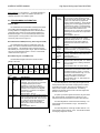
1
Series 9325
High Speed Analog Input Board With RAM
USER’S MANUAL
ACROMAG INCORPORATED
30765 South Wixom Road
P.O. BOX 437
Wixom, MI 48393-7037 U.S.A.
Tel: (248) 624-1541
Fax: (248) 624-9234
Copyright 1994, Acromag, Inc., Printed in the USA.
Data and specifications are subject to change without notice.
8500-243-A94J008
AVME9325 USER'S MANUAL
High Speed Analog Input Board With RAM
___________________________________________________________________________________________
The information contained in this manual is subject to change
without notice. Acromag, Inc. makes no warranty of any kind with
regard to this material, including, but not limited to, the implied
warranties of merchantability and fitness for a particular purpose.
Further, Acromag, Inc. assumes no responsibility for any errors that
may appear in this manual and makes no commitment to update, or
keep current, the information contained in this manual. No part of
this manual may be copied or reproduced in any form, without the
prior written consent of Acromag, Inc.
Table of Contents
1.0 GENERAL INFORMATION..............................................
KEY AVME9325 FEATURES..........................................
VMEbus INTERFACE FEATURES..................................
2.0 PREPARATION FOR USE...............................................
UNPACKING AND INSPECTION....................................
CARD CAGE CONSIDERATIONS..................................
BOARD CONFIGURATION.............................................
Default Jumper Configuration........................................
Address Decode Jumpers.............................................
Address Modifier Selection............................................
Interrupt Level Selection.................................................
Analog Input Type..........................................................
Analog Input Ranges......................................................
Analog Input Data Format..............................................
Unipolar Straight Binary.(USB)..............................
Bipolar Offset Binary (BOB) and
Bipolar Two's Complement (BTC)..........................
ANALOG INPUT CONNECTOR.......................................
EXTERNAL TRIGGER CONNECTOR.............................
TRIGGER OUTPUT CONNECTOR.................................
VMEbus CONNECTIONS.................................................
3.0 PROGRAMMING INFORMATION...................................
MEMORY MAPS...............................................................
Board Identification PROM.............................................
Board Status Register....................................................
Vector Register..............................................................
Board Control Register...................................................
Scan Programming Register..........................................
Start Conversion Register..............................................
Counter Control Register................................................
Timer Prescaler Register...............................................
Conversion Timer Register.............................................
Conversion Count Register............................................
Pre-Trigger Data Pointer................................................
Dual Port RAM...............................................................
MODES OF OPERATION.................................................
Initialization.....................................................................
Block Mode.....................................................................
Continuous Mode...........................................................
Pre-, Post-Trigger Acquisition........................................
INITIATING ANALOG-TO-DIGITAL CONVERSIONS.....
Software Triggering - Register Access..........................
External Triggering - TTL Input......................................
Timed Periodic Triggering..............................................
TRIGGER OUTPUT..........................................................
GENERAL PROGRAMMING CONSIDERATIONS..........
Board Diagnostics..........................................................
Treatment of Data..........................................................
Page
3
3
3
3
3
3
3
3
4
4
4
4
4
4
4
5
5
5
5
5
6
6
6
6
7
7
8
8
8
9
9
9
9
9
9
9
10
10
10
10
10
10
10
11
11
11
11
-2-
Table of Contents
PROGRAMMING EXAMPLES..........................................
Using the Block Mode Without Interrupts......................
Using the Block Mode With Interrupts...........................
Using the Continuous Mode With Interrupts..................
Post-Trigger Acquisition................................................
4.0 THEORY OF OPERATION...............................................
VMEbus INTERFACE.......................................................
Bus Control Logic...........................................................
VMEbus Interrupter Logic..............................................
DC-to-DC Converter.......................................................
ON BOARD ADDRESSING..............................................
Scan Program Resister..................................................
Dual Port RAM...............................................................
ANALOG INPUT SECTION..............................................
Analog Input Multiplexer.................................................
Instrumentation Amplifier................................................
Programmable Gain Circuit............................................
Sample and Hold Circuit.................................................
Analog to Digital Converter.............................................
ACQUISITION CONTROL LOGIC....................................
EXTERNAL TRIGGER......................................................
TIMED PERIODIC TRIGGER CIRCUIT...........................
TRIGGER OUTPUT..........................................................
5.0 SERVICE AND REPAIR....................................................
SERVICE AND REPAIR ASSISTANCE...........................
PRELIMINARY SERVICE PROCEDURE........................
CALIBRATION PROCEDURES.......................................
Instrumentation Amplifier Calibration.............................
Input Offset Calibration for Programmable Gain Stage..
Sample and Hold Offset Calibration..............................
± 10V Bipolar Calibration...............................................
± 5V Bipolar Calibration.................................................
Unipolar Calibration.......................................................
REPLACEABLE PARTS
6.0 SPECIFICATIONS.............................................................
GENERAL SPECIFICATIONS..........................................
ANALOG INPUT SECTION.............................................
Page
11
11
12
12
12
13
13
13
13
14
14
14
14
14
14
14
14
14
15
15
15
15
15
15
15
15
16
16
16
16
16
17
17
17
18
18
18
DRAWINGS
4500-940 Jumper Location................................................
4500-941 Connections Diagrams......................................
4500-938 AVME9325 Schematic & Parts Location...........
4500-939 AVME9325 Block Diagram...............................
Page
19
20
21
27
IMPORTANT SAFETY CONSIDERATIONS
It is very important for the user to consider the possible adverse
effects of power, wiring, component, sensor, or software failures in
designing any type of control or monitoring system. This is
especially important where economic property loss or human life is
involved. It is important that the user employ satisfactory overall
system design. It is agreed between the Buyer and Acromag, that
this is the Buyer's responsibility.
AVME9325 USER'S MANUAL
High Speed Analog Input Board With RAM
___________________________________________________________________________________________
1.0 GENERAL INFORMATION
This board is physically protected with
packing material and electrically
protected with an anti static bag during
shipment. It is recommended that the
board be visually inspected for
evidence of mishandling prior to
applying power.
Models AVME9325-10 and AVME9325-5 are 12 bit analog input
boards with on board RAM for data storage. These boards act as
VMEbus slaves with analog throughput times of 10uS and 5uS
respectively. These boards include many features which make them
an ideal choice for a broad range of analog input applications.
The board utilizes static sensitive
components and should only be
handled at a static-safe workstation.
KEY AVME9325 FEATURES
12 bit High-Speed - 12-bit A/D with 10uS per channel
•
(AVME9325-10) throughput, or 5uS per channel throughput
(AVME9325-5).
High Channel Count - High level non-isolated inputs - 16
•
Differential/32 Single-Ended (jumper selectable).
Programmable Input Ranges - Jumper Programmable Input
•
Ranges: ±5V, ±10V, 0 to 10V.
Programmable Gain - Gain x1, x2, x4, and x8.
•
Data Storage RAM - 128KB Dual Port RAM Storage Buffer.
•
Scanning - Configuration of Scan via codes in Scan Program
•
RAM. Codes allow scan order and gain to be programmed on
an individual channel basis.
Block Mode - Performs a specified number of conversions.
•
Continuous Mode - Performs conversions continuously.
•
Pre-trigger & Post-trigger acquisition - A trigger may be
•
used to stop acquisition. Acquisition is stopped by performing
the specified number of post-trigger A/D conversions.
Flexible Triggering - Internally Timed Periodic Trigger for
•
precise sampling intervals. External Trigger (BNC connector)
for synchronization with external events. Software Trigger.
BNC Trigger Output Connector - May be used to provide a
•
sync so that other boards can trigger on the same input trigger
pulse (external, internal, or timed). This provides for multiple
axis sampling.
Interrupts - Jumper programmable level, software
•
programmable vector. On the completion of a block of
conversions or as each half of dual port RAM is filled.
CARD CAGE CONSIDERATIONS
Refer to the specifications for bus loading and power
requirements. Be sure that the system power supplies are able to
accommodate the additional requirements within the voltage
tolerances specified.
IMPORTANT: Adequate air circulation must be provided to prevent
a temperature rise above the maximum operating temperature.
BOARD CONFIGURATION
The AVME9325 board may be configured in a variety of ways
for many different applications. Each possible jumper setting will be
discussed in the following sections. The jumper locations are shown
in Drawing 4500-940.
Default Jumper Configuration
A board is shipped from the factory configured as follows:
VMEbus Interface Configuration
VMEbus Standard Address of 800000H.
•
Set to respond to both Address Modifiers 39H and 3DH.
•
Interrupt Level: None. Therefore, even if interrupts are
•
enabled through the Board Status Register, no interrupts
will be caused.
VMEBUS INTERFACE FEATURES
A24:D16/D8(EO), DTB SLAVE, AM CODES: 39H, 3DH.(i.e.,
•
standard address space)
I (1-7) Interrupter - jumper programmable interrupt level,
•
software programmable interrupt vector. Release On
Acknowledge (ROAK) type.
Address decode on 256K byte boundaries (6 jumpers).
•
Analog Inputs
16 Differential Input Channels numbered 0 through 15.
•
-10V to +10V Input Range calibrated for Binary 2's
•
complement data as follows:
Analog
Input Voltage
+9.9951 V
+9.9902 V
.
.
.
+0.0049 V
0.0000 V
-0.0049 V
.
.
.
-9.9951 V
-10.0000 V
2.0 PREPARATION FOR USE
UNPACKING AND INSPECTION
Upon receipt of this product, inspect the shipping carton for
evidence of mishandling during transit. If the shipping carton is
badly damaged or water stained, request that the carrier's agent be
present when the carton is opened. If the carrier's agent is absent
when the carton is opened and the contents of the carton are
damaged, keep the carton and packing material for the agent's
inspection.
For repairs to a product damaged in shipment, refer to the
Acromag Service Policy to obtain return instructions. It is suggested
that salvageable shipping cartons and packing material be saved for
future use in the event the product must be shipped.
- 17-
A/D Data
(12 Bits Left Justified)
7FF0 H
7FE0 H
.
.
.
0010 H
0000 H
FFF0 H
.
.
.
8010 H
8000 H
AVME9325 USER'S MANUAL
High Speed Analog Input Board With RAM
___________________________________________________________________________________________
Address Decode Jumpers
Configuration
16 Channel
Differential
32 Channel
Single-Ended
The board interfaces with the VMEbus as a 256K block of
address locations in the VMEbus Standard Address space. J9
decodes the six most significant address lines A18 through A23 to
provide 64 segments of 256K address space. The configurations of
the jumpers for different base address locations are shown below.
("In" means that the pins are shorted together with a shorting clip.
"Out" indicates that the clip has been removed).
BASE
ADDR
000000H
040000H
080000H
0C0000H
100000H
Pins
11 &12
OUT
OUT
OUT
OUT
OUT
EC0000H
F00000H
F40000H
F80000H
FC0000H
.
.
IN
IN
IN
IN
IN
Pins OF J9
Pins
Pins
9 & 10
7&8
OUT
OUT
OUT
OUT
OUT
OUT
OUT
OUT
OUT
OUT
.
.
IN
IN
IN
IN
IN
.
.
IN
IN
IN
IN
IN
Pins
5&6
OUT
OUT
OUT
OUT
IN
Pins
3&4
OUT
OUT
IN
IN
OUT
Pins
2&1
OUT
IN
OUT
IN
OUT
.
.
OUT
IN
IN
IN
IN
.
.
IN
OUT
OUT
IN
IN
.
.
IN
OUT
IN
OUT
IN
Connect
Pins of J8
Connect
Pins of J2
Channel
Address
2 and 3
1 and 2,
3 and 4
None
0 thru 15
1 and 2
0 thru 31
Analog Input Ranges
The Analog Input Ranges may be selected through J3, J4, and
J5 (J5 is used only on model AVME9325-5). The basic analog input
ranges are ±10V Bipolar, ±5V Bipolar, and 0 to +10V Unipolar.
Other ranges may be obtained by changing the Software
Programmable Gain (See Board Control Register Description,
Section 3) from x1 to x2, x4 or x8. Input ranges may be
selected as follows:
Configuration
(at Gain = x1)
±10V Bipolar
± 5V Bipolar
0 to 10V Unipolar
Connect
J4 Pins
1 and 2
2 and 3
2 and 3
Connect
J3 Pins
2 and 3
2 and 3
1 and 2
(AVME 9325-5)
Connect
J5 Pins
None
None
1 and 2
Note: When changing the analog input range it will be necessary to
recalibrate the A/D Converter. See Calibration Procedures,
Section 5, for details.
Address Modifier Selection
The VMEbus Address Modifier jumper, J10, permits the board
to respond to the Address Modifier Code 3DH, the Standard
Supervisory data access, and 39H, the Standard Non-privileged data
access. With jumper J10 in place, the board will respond to 39H
and 3DH. If not in place, the board will respond only to 3DH.
Analog Input Data Format
The Analog Input Data can appear as Unipolar Straight Binary
(USB), Bipolar Offset Binary (BOB) or Bipolar Two's Complement
(BTC). The data format is determined by the Analog Input Range
and the configuration of J1.
Interrupt Level Selection
The Interrupt Level is selected by configuring Jumper J7 as
follows:
Desired
Data Format
USB
BOB
BTC
Pins OF J7
Interrupt Level
5 and 6
3 and 4
1 and 2
None
OUT
OUT
OUT
1
OUT
OUT
IN
2
OUT
IN
OUT
3
OUT
IN
IN
4
IN
OUT
OUT
5
IN
OUT
IN
6
IN
IN
OUT
7
IN
IN
IN
"IN" means that the pins are shorted together with a shorting clip.
"OUT" indicates that the clip has been removed.
Analog Input Range
Unipolar
Bipolar
Bipolar
Connect
Pins of J1
2 and 3
2 and 3
1 and 2
Assuming standard calibration, the following tables indicate the
relationship between Data Format and actual Analog Input Voltage.
Unipolar Straight Binary (USB)
USB is used for the Unipolar 0V to +10V range:
Analog Input Voltage
9.9976 V
9.9951 V
.
.
.
0.0024 V
0.0000 V
Analog Input Type
The AVME9325 board can accept either 16 channels of
differential input or 32 channels of single-ended input. The selection
is made by configuring J8 and J2 as follows:
USB Data
FFF0 H
FFE0 H
.
.
.
0010 H
0000 H
Bipolar Offset Binary(BOB) & Bipolar Two's Complement(BTC)
BOB & BTC are used for the bipolar -10V to +10V and -5V to +5V
analog input ranges:
- 17-
AVME9325 USER'S MANUAL
High Speed Analog Input Board With RAM
___________________________________________________________________________________________
± 10V
+9.9951 V
+9.9902 V
.
.
.
+0.0049 V
0.0000 V
-0.0049 V
.
.
.
-9.9951 V
-10.0000 V
± 5V
+4.9976 V
+4.9952 V
.
.
.
+0.0024 V
0.0000 V
-0.0024 V
.
.
.
-4.9976 V
-5.0000 V
BOB Data
FFF0 H
FFE0 H
.
.
.
8010 H
8000 H
7FF0 H
.
.
.
0010 H
0000 H
EXTERNAL TRIGGER CONNECTOR
BTC Data
7FF0 H
7FE0 H
.
.
.
0010 H
0000 H
FFF0 H
.
.
.
8010 H
8000 H
The External Trigger signal is connected to the AVME9325
board via a front-panel BNC connector (P3). Analog-to-Digital
conversions may be synchronized to external events using an
external trigger source. The External Trigger must be a debounced
TTL compatible signal. A conversion is triggered on the falling edge
of a low pulse. A 100 nanosecond minimum low pulse width is
required.
TRIGGER OUTPUT CONNECTOR
A trigger output signal is provided via a front panel BNC
connector (P4). This signal may be used to provide a sync, so that
other boards can trigger on the same input pulse (external, software,
or timed-periodic triggering). This provides for multi-axis sampling.
An output trigger pulse occurs whenever a Software Trigger occurs
if the Software Trigger type has been selected. Likewise, an output
trigger pulse will occur whenever an External Trigger occurs if the
external trigger type has been selected. The internally generated
Timed Periodic Triggers will also cause output triggers.
ANALOG INPUT CONNECTOR
Analog inputs are connected to the AVME9325 board via
Connector P2. Table 2.1 defines the pin assignment. These
connections can be easily accommodated through the use of
Acromag Termination Panels and Ribbon Cable Assemblies or
through the use of a user defined Termation Panel. Note: Ribbon
cable length should be kept under ten feet to avoid noise problems.
VMEbus CONNECTIONS
Figures 2.2 & 2.3 of 4500-941 illustrate methods for connecting
analog signals to the board. Refer to Section 2 (Analog Input Type)
for details concerning the correct jumper configuration for each input
type. A Sense input is provided for single-ended inputs and is
connected to the "-" input of the instrumentation amplifier when the
board is configured for single-ended inputs. Connect the Sense
input to signal common for single-ended operation. Note that for
both single-ended and differential operation, this input must be
referenced to analog (system) common for the instrumentation
amplifier to function properly. Connection to analog common is
available at the P2 connector (COM).
Table 2.1: P2 Connector (Single-Ended & Differential):
SINGLE
DIFFER
Pin
Pin
DIFFER
8A
8C
SHIELD
NC
NC
COM
COM
9A
9C
COM
CH30 In
-CH14 In
10A
10C
-CH15 In
CH22 In
+CH14 In
11A
11C
+CH15 In
SENSE
12A
12C
CH28 In
-CH12 In
13A
13C
-CH13 In
CH20 In
+CH12 In
14A
14C
+CH13 In
15A
15C
NC
NC
NC
CH26 In
-CH10 In
16A
16C
-CH11 In
CH18 In
+CH10 In
17A
17C
+CH11 In
18A
18C
NC
NC
NC
CH24 In
-CH8 In
19A
19C
-CH9 In
CH16 In
+CH8 In
20A
20C
+CH9 In
21A
21C
NC
NC
NC
CH14 In
-CH6 In
22A
22C
-CH7 In
CH6 In
+CH6 In
23A
23C
+CH7 In
24A
24C
NC
NC
NC
CH12 In
-CH4 In
25A
25C
-CH5 In
CH4 In
+CH4 In
26A
26C
+CH5 In
27A
27C
NC
NC
NC
CH10 In
-CH2 In
28A
28C
-CH3 In
CH2 In
+CH2 In
29A
29C
+CH3 In
+BIAS
+BIAS
30A
30C
-BIAS
CH8 In
-CH0 In
31A
31C
-CH1 In
CH0 In
+CH0 In
32A
32C
+CH1 In
NOTE: “NC” denotes No Connection.
Table 2.2 indicates the P1 pin assignments for the VMEbus
signals. The P1 connector is the upper connector on the board as
viewed from the front. The connector consists of 32 rows of three
pins labeled A, B, and C. Pin A1 is located at the upper left hand
corner of the connector.
Table 2.2: P1 Bus Signals
PIN
DESCR.
PIN
1A
D00
1B
2A
D01
2B
3A
D02
3B
4A
D03
4B
5A
D04
5B
6A
D05
6B
7A
D06
7B
8A
D07
8B
9A
GND
9B
10A
SYSCLK
10B
11A
GND
11B
12A
DS1*
12B
13A
DS0*
13B
14A
WRITE*
14B
15A
GND
15B
16A
DTACK*
16B
17A
GND
17B
18A
AS*
18B
19A
GND
19B
20A
IACK*
20B
21A
IACKIN*
21B
22A
IACKOUT*
22B
23A
AM4
23B
24A
A07
24B
25A
A06
25B
26A
A05
26B
27A
A04
27B
28A
A03
28B
29A
A02
29B
30A
A01
30B
31A
-12V
31B
32A
+5V
32B
SINGLE
SHIELD
COM
CH31 In
CH23 In
SENSE
CH29 In
CH21 In
NC
CH27 In
CH19 In
NC
CH25 In
CH17 In
NC
CH15 In
CH7 In
NC
CH13 In
CH5 In
NC
CH11 In
CH3 In
-BIAS
CH9 In
CH1 In
- 17-
DESCR.
BBSY*
BCLR*
ACFAIL*
BG0IN*
BG0OUT*
BG1IN*
BG1OUT*
BG2IN*
BG2OUT*
BG3IN*
BG3OUT*
BR0*
BR1*
BR2*
BR3*
AM0
AM1
AM2
AM3
GND
SERCLK (#)
SERDAT*(#)
GND
IRQ7*
IRQ6*
IRQ5*
IRQ4*
IRQ3*
IRQ2*
IRQ1*
+5V STDBY
+5V
PIN
1C
2C
3C
4C
5C
6C
7C
8C
9C
10C
11C
12C
13C
14C
15C
16C
17C
18C
19C
20C
21C
22C
23C
24C
25C
26C
27C
28C
29C
30C
31C
32C
DESCR.
D08
D09
D10
D11
D12
D13
D14
D15
GND
SysFAIL*
BERR*
SysRESET*
LWORD*
AM5
A23
A22
A21
A20
A19
A18
A17
A16
A15
A14
A13
A12
A11
A10
A09
A08
+12V
+5V
AVME9325 USER'S MANUAL
High Speed Analog Input Board With RAM
___________________________________________________________________________________________
Notes (Table 2.2): # - No connection; * - An asterisk indicates that
the signal is active low. Refer to the VMEbus specification for
additional information on the VMEbus signals.
BIT
Bit 5
NAME
Missed
Trigger
Input (R)
Bit 4
Software
Reset
(W)
3.0 PROGRAMMING INFORMATION
MEMORY MAPS
The AVME9325 board is addressable on 256K byte boundaries
in the VMEbus Standard Address space (See Section 2). All
Acromag VMEbus non-intelligent slaves have a standard interface
configuration which consists of a 32 byte board ID PROM and a
Board Status Register. The rest of the 256K byte address space
contains registers or memory specific to the function of the board.
The memory map is shown in Figure 3.1.
Board Identification PROM (Read Only, 01H through 3FH ODD)
The AVME9325 board contains an identification section (ID
PROM). This section of data describes the board model number
and manufacturer. The identification section starts at the board's
base address plus 1 and is 32 bytes in length. Bytes are addressed
using only the odd addresses between 1 and 63. The ID PROM
contents are shown in Figure 3.2.
Bit 3
Bit 2
Board Status Register - (Read/Write, 81H)
Bit 1
The Board Status Register reflects and controls functions
globally on the board.
MSB
7
Acq
Comp
6
Memory
5
Miss
Trig.
Input
Where:
BIT
NAME
Bit 7
Acquisition
Complete
(R)
Bit 6
Memory
(R)
4
SW
Reset
3
Global
Int.
Enable
2
Global
Int.
Pend.
1
Grn.
LED
LSB
0
Red
LED
Bit 0
DESCRIPTION
This bit is set to a "1" when a programmed
sequence of data acquisitions has been
completed. This bit is set to a "0" at the start
of a programmed sequence of data
acquisitions. This bit can be polled to
determine when the number of conversions
specified in the Conversion Count Register
(see Section 3, Conversion Count Register)
has been completed.
Reset Condition: Set to “0”.
This bit is set to a "0" when the first half of the
Dual Port RAM Data Storage Buffer has been
most recently filled with data. This bit is set to
a "1" when the second half has been most
recently filled. This bit can be polled to
determine when half of the data buffer has
been filled.
Reset Condition: Set to "1"
Global
Interrupt
Enable
(R/W)
Global
Interrupt
Pending
(R)
Green
LED
(R/W)
Red LED
(R/W)
DESCRIPTION
This bit is set to a "1" if a trigger occurs after an
A/D conversion has been initiated and before
the next channel has had time to settle. This bit
is set to a "0" at the start of a programmed
sequence of data acquisitions. This bit will flag
triggering errors such as triggering faster than
the hardware can support. This bit will also be
set to a "1" if a trigger occurs in the block mode
when the value in the Conversion Count
Register is zero (i.e., perform zero conversions)
indicating that a conversion was not performed
on the trigger.
Reset Condition: Set to "0".
Writing a "1" to this bit causes a software reset.
Writing "0" or reading the bit has no effect.
This bit will always read as a "0". The effect of
a software reset on the various registers is
determined in the discussion of each of the
registers.
Writing a "1" to this bit enables interrupts to
occur from the board. A "0" prevents interrupts.
Reset Condition: Set to "0", interrupts disabled.
This bit will be a "1" when there is an interrupt
pending. This bit will be "0" when there is no
interrupt pending.
Reset condition: Set to "0".
This bit, when written, will control the state of
the green LED on the front panel. A "1" will turn
it on, a "0" will turn it off. Reading it will reflect
its current state.
Reset Condition: Set to "0", Green LED off.
This bit, when written, will control the state of
the Red LED on the front panel and the state of
the VMEbus SYSFAIL* signal. A "1" will turn
the LED off and set SYSFAIL* high, a "0" will
turn the LED on and set SYSFAIL* low.
Reading it will reflect its current state.
Reset Condition: Set to "0", Red LED lit, and
SYSFAIL* is set low.
The Status Register bits 1 and 0 along with the green and red
LEDs provide the user with a means of keeping track of a board's
functionality in the system. Since there is no intelligence on the
board, the host computer controls these bits. The following
paragraphs are possible uses of the bits in the status register and
the LEDs on the front panel.
On power-up, the status register bits read low, the green LED is
OFF, the red LED ON, and the SYSFAIL* signal is low. This
indicates that the board has failed or that it hasn't been tested yet.
The Status Register Bit 1 reads low and Bit 0 reads high. The
LEDs will both be off and SYSFAIL* is high. This indicates an
inactive board.
The Status Register Bit 1 reads high and Bit 0 reads low. The
LEDs will both be lit and SYSFAIL* is low. This indicates the board
is undergoing a diagnostic checkout.
- 17-
AVME9325 USER'S MANUAL
High Speed Analog Input Board With RAM
___________________________________________________________________________________________
The Status Register Bits 1 and 0 read high. The Green LED will
be ON with the Red LED OFF and SYSFAIL* HIGH. This indicates
the board is fully functional.
Figure 3.1: Analog Input Board Memory Map
EVEN
Base
EVEN Byte
ODD Byte
Addr.+
D15
D08
D07
D00
READ - Module ID
00
UNDEFINED
PROM
↓
3E
40
UNDEFINED
↓
7E
R/W - Board Status
80
Figure 3.2: Analog Input Board Identification (ID) PROM
Hex Offset
ASCII
Numeric
From Board
Character
Value
Base Address Equivalent
(Hex)
Field Description
01
V
56
All VME Boards
03
M
4D
Have
05
E
45
“VMEID”
07
I
49
09
D
44
ODD
Base
Addr.+
01
↓
3F
41
↓
7F
81
82
R/W - Vector
84
R/W - Board
Control
83
85
86
W - Scan Program
88
W - Start Conversion
8A
W - Timer Prescaler
8C
W - Conversion
Timer
8E
W - Counter Control
0B
0D
0F
A
C
R
41
43
52
Manufacturer
ID - “ACR” for
Acromag
11
13
15
17
19
1B
1D
9
3
2
5
1
0
39
33
32
35
2D
31
30
Board Model No.
Unique for Each
Model
1F
0
30
Number of Kbytes
of Address Space
Used. If equal “0”,
then Address
Space is indicated
at byte 29H.
87
89
21
23
20
20
25
27
20
20
8B
29
2B
2D
2F
8D
0
2
5
6
30
32
35
36
Four Bytes indicating the number of
Kbytes of address
space used (256
for example)
8F
31-3F
90
Undefined
Reserved
W - Conversion Count
91
Vector Register (Read/Write, 83H)
92
The Vector Register maintains the 8 bit interrupt vector which is
provided to the VMEbus Interrupt Handler when an interrupt is being
serviced. The register content is undefined upon reset.
R- PreTrigger Data Pointer
94
↓
1FFFE
20000
↓
3FFFE
Undefined
R/W - Dual Port RAM
93
95
↓
1FFFF
20001
↓
3FFFF
Board Control Register (Read/Write, 85H)
The Control Register contains bits which are used to control
how the board functions.
BOARD CONTROL REGISTER:
MSB
_
_
_
_
_
7
6
5
4
3
2
< ---------RESERVED------- >
CNTEN TRIG
TYPE
- 17-
_
LSB
1
0
INT. MODE
TYPE
AVME9325 USER'S MANUAL
High Speed Analog Input Board With RAM
___________________________________________________________________________________________
Where:
BIT
Bits 4 - 7*
Bit 3*
Bit 2*
Bit 1*
Bit 0*
NAME
CNTEN
Trigger
Type
Interrupt
Type
Mode
Where:
BIT
Bit 7
DESCRIPTION
Reserved - read as "0"
Conversion Timer Enable. A "0"
disables the timer. Writing a "1" to this
bit enables the conversion timer circuit.
See section 3 (Timed Periodic
Triggering).
A "0" selects on-board Software
Triggering via the Start Conversion
Register. A "1" selects External
Triggering.
This bit selects which event will cause
an interrupt when interrupts are
enabled. See section 3 (Board Status
Register) for information on how to
enable interrupts. A "0" will select
Acquisition Complete Interrupts to
occur at the end of a programmed
sequence of data acquisitions, in other
words when the number of conversions
specified in the Conversion Count
Register have been completed.
Acquisition Complete Interrupts will
usually be used in the Block Mode of
operation. A "1" will select Memory
Interrupts to occur after filling each half
of the Dual Port RAM data buffer.
Memory Interrupts will usually be used
in the Continuous mode of operation.
This bit selects the mode in which the
board will operate. See section 3
(Modes of Operaton) for a detailed
discussion of operating modes. The
modes are selected as follows:
MODE
0
1
Bits 5 & 6
NAME
EOS
GAIN
DESCRIPTION
End Of Scan. A "1" indicates to the scan
sequencer that the memory location is the
last one to be used for the group of
channels to be scanned.
These bits select the gain at which the
specified analog input channel will be
read. The Gains are selected as follows:
BIT 6 BIT 5
0
0
0
1
1
0
1
1
Bits 0-4
GAIN
x1
x2
x4
x8
These bits contain the channel number of
the analog input channel to be read.
Reset Condition: Undefined
Start Conversion Register (Write Only, 89H)
The Start Conversion Register is a write-only register and is
used to trigger a conversion when software triggering has been
selected with Bit 2 of the Control Register.
START CONVERSION REGISTER:
MSB
_
_
_
_
_
7
6
5
4
3
2
X
X
X
X
X
X
NOTE: "X" means the bit value does not matter.
_
1
X
LSB
0
X
Counter Control Register (Write Only, 8FH)
The Counter Control Register is used to set up the on-board
counter device when timed periodic conversions are desired.
DESCRIPTION
Block Mode: Convert x times
Continuous Mode: Convert
Continuously
COUNTER CONTROL REGISTER:
MSB
_
_
_
_
_
_
LSB
7
6
5
4
3
2
1
0
<--------------------------Counter Control Codes---------------------------->
The number of times converted is equal
to the value the user has written into the
Conversion Count Register.
Four Counter Control Codes may be written into this register:
CODE
54H
* Reset condition: All bits set to "0"
Scan Programming Register - (Write Only, 87H)
74H
This Register is used to configure the order in which channels
are scanned. It is also used to configure the gain at which each
channel will be converted. There are 256 Scan Program memory
locations accessible through this register. See section 3 (Modes of
Operation) for programming information. The format for each
memory location is as follows:
94H
B4H
SCAN PROGRAMMING REGISTER:
MSB
_
_
_
_
_
_
LSB
7
6
5
4
3
2
1
0
EOS
< GAIN >
<------ CHANNEL NUMBER------>
FUNCTION
Sets up the on-board counter device to
receive the single byte prescaler count in
the Timer Prescaler Register.
Sets up the on-board counter device to
receive the two byte prescaler count in
the Timer Prescaler Register.
Sets up the on-board counter device to
receive the single byte timer count in the
Conversion Timer Register.
Sets up the on-board counter device to
receive the two byte timer count in the
Conversion Timer Register.
See Section 3 (Timed Periodic Triggering) for a detailed
discussion on timed-periodic conversions. The register content is
undefined upon reset.
- 17-
AVME9325 USER'S MANUAL
High Speed Analog Input Board With RAM
___________________________________________________________________________________________
Timer Prescaler Register (Write Only, 8BH)
The Timer Prescaler Register is used to hold the Prescaler
Count.
PRETRIGGER DATA POINTER:
MSB _ _ _ _ _ _ _
_ _ _ _ _ _ _ LSB
15 14 13 12 11 10 9 8
7 6 5 4 3 2 1 0
<-------------------------Pre-Trigger Data Pointer--------------------------->
TIMER PRESCALER REGISTER:
MSB
_
_
_
_
_
_
LSB
7
6
5
4
3
2
1
0
<------------------------PRESCALER COUNT----------------------------->
This register contains a 16-bit number between 0 and 65535
(64K). To find the corresponding address in the 128K of Dual Port
RAM, this number is multiplied by 2 then added to the starting
address of Dual Port RAM.
This 8 or 16-bit number divides a 2 MHz clock signal. The clock
signal is further divided by the number held in the Conversion Timer
Register and the resulting frequency is used to generate periodic
triggers for precisely timed intervals between conversions. A 16-bit
Prescaler Count is entered by writing the least significant byte and
then the most significant byte. The register content is undefined
upon reset.
EXAMPLE: Suppose this register contains the value 1111H, the
corresponding VMEbus address is found by:
Base Address + 20000H + 2(1111H) = Base Address + 22222H.
Where:
Base Address is the base address of the board in the
VMEbus Standard Address range.
20000H is the offset on board to the Dual Port RAM area.
Conversion Timer Register (Write Only, 8DH)
Reset Condition: Undefined
The Conversion Timer Register is used to hold the Timer Count.
Dual Port RAM - (Read/Write, 20000H through 3FFFFH)
CONVERSION TIMER REGISTER:
MSB
_
_
_
_
_
_
LSB
7
6
5
4
3
2
1
0
<------------------------------TIMER COUNT--------------------------------->
Dual Port RAM (128K Bytes) is used to hold the analog input
data. The exact location of the data for each channel is dependent
upon which Mode has been selected and what channels are
included in the scan if scanning has been selected. Data is stored in
Dual Port RAM starting at the lowest address (base address +
20000H). The following data is stored in the next available 16-bits of
memory in an increasing fashion.
This 8 or 16 bit number is the second divisor of a 2MHz clock
signal and is used together with the Timer Prescaler Register to
derive the frequency of periodic triggers for precisely timed intervals
between conversions. A 16-bit Timer Count is entered by
consecutively writing the least significant byte and then the most
significant byte. The register content is undefined upon reset.
Each 16-bit data location in Dual Port RAM will have the
following format:
Conversion Count Register (Write Only, 90H and 91H)
DUAL PORT RAM:
MSB _ _ _ _ _ _ _
_ _ _ _
15 14 13 12 11 10 9 8
7 6 5 4
<------------------Analog Input Data---------------------->
The Conversion Count Register is used to hold the number of
times to perform an A/D conversion in the Block Mode of operation.
It is also used to hold the number of post-trigger A/D conversions to
perform when a trigger is used to stop acquisition in the Continuous
Mode of operation. The Counter must be re-written after it is used.
_
3
0
_ _ LSB
2 1 0
0 0 0
MODES OF OPERATION
Reset condition : Undefined
There are 2 programmable Modes of Operation. In either mode
a single channel or a sequence of channels may be converted. The
initialization required for both modes and a description of the use of
each mode is discussed below.
CONVERSION COUNT REGISTER:
MSB _ _ _ _ _ _ _
_ _ _ _ _ _ _ LSB
15 14 13 12 11 10 9 8
7 6 5 4 3 2 1 0
<---------------------------Conversion Count---------------------------------->
Initialization:
Initialize interrupt vector and enable interrupts if desired.
•
If timed periodic conversions are desired, set up the Counter
•
Control, Timer Prescaler, and Conversion Timer Registers as
necessary. (See Section 3, Timed Periodic Triggering).
Write the correct code to the Control Register for the desired
•
Mode, type of interrupts and type of triggering.
Consecutively write Scan Codes into the Scan Program
•
Register for each channel to be included as part of the Scan.
Channels may be repeated. The total number of channels to be
scanned as a sequence may be as large as 256. BIT 7 (EOS
bit) of the Scan Code of the last channel in the sequence must
be '1'. Single channel operation can be programmed by setting
the EOS bit in the Scan Code for the desired channel and
writing only this Scan Code to the Scan Program Register.
Pre-Trigger Data Pointer - (Read Only, 92H and 93H)
The Pre-Trigger Data Pointer is used to find the location in Dual
Port RAM of the most recent "pre-trigger" A/D data. If a trigger is
used to stop acquisition in the Continuous Mode (See Section 3,
Pre-, Post-Trigger Acquisition) this register can be used to find the
location of the data from the A/D conversion completed just prior to
receiving the trigger. In this way the Dual Port RAM Data Buffer can
be accurately divided into pre- and post-trigger data. During normal
data acquisition this register can be used to find the location of the
most recent A/D data.
- 17-
AVME9325 USER'S MANUAL
High Speed Analog Input Board With RAM
___________________________________________________________________________________________
Block Mode
INITIATING ANALOG-TO-DIGITAL CONVERSIONS
The Block Mode is used to perform A/D conversions the number
of times specified in the Conversion Count Register. Usage is:
Analog-to-Digital conversions may be initiated or triggered in
three different ways. Each way has advantages which will be
discussed in the following subsections.
•
•
•
•
Write the desired number of conversions into the
Conversion Count Register.
Perform a Write operation to the Start Conversion Register
if Software Triggering has been selected or wait for an
External Trigger. If Timed Periodic Triggering has been
selected, then only one Software or External Trigger
should be given. See Section 3 (Timed Periodic
Triggering).
Poll the Board Status Register until the Acquisition is
complete or wait for an interrupt if Acquisition Complete
interrupts have been enabled.
Read data from the Dual Port RAM.
Software Triggering - Register Access
Conversions may be triggered by performing a byte write to the
Start Conversion Register after having enabled Software Triggering
via bit 2 of the Board Control Register. The value of the byte written
does not matter. This method of starting a conversion is most useful
for its simplicity and for when precise time of conversion is not
critical. Typically, Software Triggering is only used for initiating the
first conversion in any of the modes. Be aware that writing a byte at
a precise point in time may be difficult in a multi-tasking system or in
a system with an arbitrated bus.
Continuous Mode
External Triggering - TTL Input
The Continuous Mode is used to perform A/D conversions
continuously. Usage is:
Conversions may be triggered by an external TTL compatible
signal input through the BNC connector on the front panel (P3).
External triggering is enabled via bit 2 of the Board Control Register.
The conversion is initiated on the falling edge of the External Trigger
Signal. See Section 2 (External Trigger Connector) for additional
specifications for this input. This type of conversion triggering is
useful for synchronizing the A/D conversion of analog inputs to
external events.
•
•
•
•
Perform a write operation to the Start Conversion Register
if Software Triggering has been selected or wait for an
External Trigger. If Timed Periodic Triggering has been
selected, then only one Software or External Trigger should
be given. See Section 3 (Timed Periodic Triggering).
Poll the Board Status Register to determine when half of
the Dual Port RAM is full or wait for an interrupt if Memory
interrupts have been enabled.
Read data from the Dual Port RAM.
Repeat.
Precise time intervals between conversions can be achieved
with an external timing device. This can also be accomplished with
Timed Periodic Triggering described in the next subsection.
Timed Periodic Triggering
Pre-Trigger & Post-Trigger Acquisition
Timed periodic triggering can be used to achieve precise time
intervals between conversions. An on-board conversion timer device
must be configured for the desired time interval. The first trigger
must be provided by a Software or External Trigger and thereafter
these triggers are ignored except for a special case (see section 3,
Pre-, Post-Trigger Acquisition). After the first trigger causes a
conversion, subsequent conversions will be caused by the timer.
Triggering will continue until the conversion timer is disabled or the
programmed function is complete.
When using Timed Periodic Triggering in the Continuous Mode,
a trigger may be used to signal when to stop acquisition. A user
trigger (Software or External) is used to start Timed Periodic
Triggering. A second user trigger (Stop Trigger) will cause the
board operation to change from Continuous to Block Mode. The
Conversion Counter contains the number of post-trigger conversions
to be performed. The Pre-Trigger Data Pointer will point to the
address in Dual Port RAM of the data obtained just prior to the Stop
Trigger. In this way the Dual Port RAM Data Buffer can be divided
into pre-trigger and post-trigger data acquisitions. Usage is:
•
•
•
•
•
The conversion timer is implemented by cascading two
counters. The first counter, the Prescaler, is clocked by a 2 MHz
clock signal. The output of this counter is input to the second
counter, the Conversion Timer, and the output is used to generate
periodic trigger pulses. The time period between trigger pulses is
described by the following equation:
Set up for timed periodic conversions.
Write the desired number of post-trigger conversions into
the Conversion Count Register.
Perform a Write operation to the Start Conversion Register
if Software Triggering has been selected or wait for an
External Trigger to start the acquisition sequence.
Perform a Write operation to the Start Conversion Register
if Software Triggering has been selected or wait for an
External Trigger to stop the acquisition sequence.
Poll the Board Status Register until the Acquisition is
complete or wait for an interrupt if Acquisition Complete
interrupts have been enabled.
T = [(N1)•(N2)] ÷ 2
Where:
T = time period between trigger pulses in microseconds.
N1 = Prescaler Count (8 or 16 bit)
N2 = Conversion Timer count (8 or 16 bit)
As can be seen, the maximum period of time which can be
programmed to occur between conversions is 2147 seconds:
[(65535)•( 65535)]÷2 = 2.147 x 10⁹ uS = 2147s or 35min & 47s.
- 17-
AVME9325 USER'S MANUAL
High Speed Analog Input Board With RAM
___________________________________________________________________________________________
After testing each board the system software records which
boards have failed and sets their status to indicate "inactive". By
setting the boards status to inactive, the SYSFAIL* signal is
released and may then be useful for an on-line indication of failure by
other boards. Alternatively, the system software could simply set
the bits and therefore front panel LEDs, to "passed test" as a visual
indication that the presence of the board is recognized.
The minimum period is not defined by the counters but is
defined by the maximum conversion rate of the hardware.
Conversions may occur as frequently as once every 10
microseconds for model AVME9325-10, or once every 5
microseconds for model AVME9325-5. The value written into either
counter must not be less than 2.
The following is the order of steps necessary to setup and
activate the Conversion Timer using an 8-bit Prescaler Count and a
16-bit Timer Count:
Treatment of Data
The input data is 12 bit left justified. When working with bipolar
signals, the user may find it advantageous to treat the data as 16 bit
two's complement numbers. In that way future products with higher
resolution A/D and D/A converters may use the same software
drivers. Similarly, unipolar data may best be treated as 16 bit
unsigned numbers.
1. Write 54H into the Counter Control Register.
2. Write the Prescaler Count (N1) into the Timer Prescaler
Register.
3. Write B4H into the Counter Control Register.
4. Write the least significant byte of the Timer Count (N2) into the
Conversion Timer Register.
5. Write the most significant byte of the Timer Count (N2) into the
Conversion Timer Register.
6. Enable the Conversion Timer by writing a "1" into bit 3 (CNTEN)
of the Board Control Register.
7. Start timed periodic conversions with a single Software or
External Trigger.
PROGRAMMING EXAMPLES
The following examples detail the programming steps required
to configure the board for various functions.
Using Block Mode Without Interrupts & With Ext. Triggering
The objective of this example is to perform 256 A/D conversions
of a single channel (channel 0) at unity gain. The conversions are to
be synchronized to an External Trigger signal. The following steps
are required to configure the Board for this function:
TRIGGER OUTPUT
A BNC connector is provided for a trigger output pulse. This
active low pulse will be asserted whenever any one of the three types
of triggers mentioned above occur. This pulse may be used to
provide a sync so that other boards can trigger on the same input
trigger pulse. This provides for multi-axis sampling.
1. Write 03H to the Status Register:
Turns off the Red LED and negates SYSFAIL* (Bit 0 = 1).
•
Turns on the Green LED (Bit 1 = 1).
•
Disables Interrupts (Bit 3 = 0).
•
2. Write 04H to the Board Control Register:
Selects Block Mode (Bit 0 = 0).
•
Selects External Trigger Type (Bit 2 = 1).
•
Disables Timed Periodic Triggering by disabling the
•
Conversion Timer (Bit 3 = 0).
Note that External Triggers should not be used until the board is
completely configured. Therefore, if the External Trigger input
will be unstable at any time during board configuration, Software
Triggering should be selected until the board is completely
configured. Then, after configuration, External Triggering
should be selected.
3. Write 80H to the Scan Program Register:
Channel 0 (Bits 0-4 = 0).
•
Gain of 1 (Bits 5-6 = 0).
•
Last channel in the scan sequence (since there is only one
•
channel Bit 7 = 1).
4. Write 100H (256 conversions) to the Conversion Count Register.
The board is now configured for the described function and will
cause A/D conversions on each falling edge of the External
Trigger signal. Note that the External Trigger signal frequency
should not be higher than the maximum sampling frequency of
the board (200K samples/s for AVME9325-5, 100K samples/s
for AVME9325-10).
5. Continuously read the contents of the Status Register until bit 7
is set to "1" indicating 256 A/D conversions have been done.
Note this bit will not be cleared to "0" until the first External
Trigger or a reset occurs if it was set prior to configuring the
board.
GENERAL PROGRAMMING CONSIDERATIONS
Board Diagnostics
The Analog Input Board is a non-intelligent slave and does not
perform self diagnostics. It does, however, provide a standard
interface architecture which includes a Board Status Register useful
in system diagnostics. Refer to section 3 (Board Status Register).
Status bits, control of front panel LEDs, and control of the
SYSFAIL* signal are provided through the Board Status Register.
Bits 0 and 1 may be used as follows:
BOARD
STATUS REG.
BIT 1
BIT 0
0
0
LED’s
GRN
RED
OFF
ON
SYSFAIL*
SIGNAL
ON
1
0
ON
ON
ON
1
0
1
1
ON
OFF
OFF
OFF
OFF
OFF
CONDITION
Board failed test or
has not been tested
Board is being
tested
Board passed test
Board is inactive
At power up, the system diagnostic software can test each nonintelligent slave, sequencing the status bits to indicate "undergoing
test" and then to "passed" or "failed".
- 17-
AVME9325 USER'S MANUAL
High Speed Analog Input Board With RAM
___________________________________________________________________________________________
1. Write OBH to the Status Register:
Turns off the Red LED and negates SYSFAIL* (Bit 0 = 1).
•
Turns on the Green LED (Bit 1 = 1).
•
Enables Interrupts (Bit 3 = 1).
•
2. Write 07H to the Board Control Register:
Selects Continuous Mode (Bit 0 = 1).
•
Selects Memory Interrupts (interrupts are caused as each
•
half of Dual Port RAM is filled) (Bit 1 = 1).
Selects External Trigger Type (Bit 2 = 1).
•
Disables Timed Periodic Triggering by disabling the
•
Conversion Timer (Bit 3 = 0).
Note that external triggers should not be used until the board is
completely configured. Therefore, if the External Trigger input
will be unstable at any time during board configuration, Software
Triggering should be selected until the board is completely
configured. Then, after configuration, external triggering should
be selected.
3. Consecutively write the following Scan Codes to the Scan
Program Register: 00, 01, 02, 03, 04, 05, 06, 07, 08, 09, 0AH,
0BH, 0CH, 0DH, 0EH and 8FH. These Scan Codes represent
channels 0 through 15 at unity gain with channel 15 being the
end of scan (Bit 7 = 1).
6. Read 256 consecutive 16-bit data samples from Dual Port RAM
starting at the board's base address plus 20000H. The 12-bit
A/D data is left justified in each 16-bit sample.
Using the Block Mode With Interrupts and Timed Periodic
Triggering.
The objective of this example is to perform a total of 65535 A/D
conversions on two channels (channel 0 and channel 8) each at
unity gain. The conversions are to occur at the maximum sampling
rate (5 microseconds assuming AVME9325-5) by utilizing Timed
Periodic Triggering. When 65535 conversions have been
completed, the board will cause an interrupt. The following steps are
required to configure the board for this function:
1. Write 0BH to the Status Register:
Turns off the Red LED and negates SYSFAIL* (Bit 0 = 1).
•
Turns on the Green LED (Bit 1 = 1).
•
Enables Interrupts (Bit 3 = 1).
•
2. Write the desired interrupt vector to the Vector Register.
3. Write 08H to the Board Control Register:
Selects Block Mode (Bit 0 = 0).
•
Selects Acquisition Complete interrupts (Bit 1 = 0).
•
Selects Software Trigger Type (Bit 2 = 0).
•
Enables Timed Periodic Triggering by enabling the
•
Conversion Timer (Bit 3 = 1).
4. Write 00H to the Scan Program Register:
Channel 0 (Bits 0-4 = 0).
•
Gain of 1 (Bits 5-6 = 0).
•
5. Write 88H to the Scan Program Register:
Channel 8 (Bits 0-4 = 8H).
•
Gain of 1 (Bits 5-6 = 0).
•
End of Scan (Bit 7 = 1).
•
6. Write FFFFH (65535) to the Conversion Count Register.
7. Program Conversion Timer for 5 microseconds:
a) Write 54H to the Counter Control Register.
b) Write 02H to the Timer Prescaler.
c) Write 94H to the Counter Control Register.
d) Write 05H to the Conversion Timer.
8. Write any byte value to the Start Conversion Register to start the
acquisition.
The board is now configured for the described function and will
cause A/D conversions on each falling edge of the External Trigger
Signal. Note that the External Trigger Signal frequency should not
be higher than the maximum sampling frequency of the board (200K
samples/s for AVME9325-5, 100K samples/s for AVME9325-10).
The board will now cause an interrupt after 32768 (32K) A/D
conversions, indicating that the first half of the Dual Port RAM has
been filled with A/D data. The board will again cause an interrupt
after another 32K A/D conversions, indicating that the second half of
the Dual Port RAM has been filled with A/D data. Interrupts will be
generated in this manner after each half of the Dual Port RAM is
filled with A/D data (multiples of 32K A/D conversions).
The Memory Bit (Bit 6 of the Status Register) can be checked to
determine which half of the Dual Port RAM has been most recently
filled with A/D data. The Interrupt Service Routine may then read
32K consecutive 16-bit data samples from Dual Port RAM starting at
the board's base address plus 20000H if the memory bit is a "0", or
starting at the board's base address plus 30000H if the memory bit
is a "1", each time an interrupt occurs. The 12-bit A/D data is left
justified in each 16-bit sample.
The Software Trigger initiates the acquisition sequence by
causing an A/D conversion of channel 0. Thereafter, the Conversion
Timer will cause A/D conversions every 5 microseconds alternating
between channel 8 and back to channel 0. This continues until
65535 A/D conversions have been completed. Upon completion the
Board will cause an interrupt request at the jumper selected interrupt
level. The Interrupt Service Routine may then read the data from
Dual Port RAM starting at the board's base address plus 20000H.
Continuous Acquisition may be halted by disabling the trigger
source (switching to Software Triggering).
Post-Trigger Acquisition
The objective of this example is to perform A/D conversions
continuously on one channel (channel 0) until the user triggers the
board to stop. Upon receiving this stop trigger, the board will
perform 1024 (1K) more A/D (post-trigger) conversions before
stopping, thus dividing the 65536 (64K) A/D data samples in Dual
Port Ram into 63K pre-trigger and lK post-trigger samples. The
conversions are to occur at a precise sampling rate of 100
microseconds through the use of Timed Periodic Triggering.
Using the Continuous Mode With Interrupts and External
Triggering.
The objective of this example is to continuously perform A/D
conversions on all 16 channels at unity gain. The conversions are to
be synchronized to an External Trigger signal. The following steps
are required to configure the board for this function:
- 17-
AVME9325 USER'S MANUAL
High Speed Analog Input Board With RAM
___________________________________________________________________________________________
4.0 THEORY OF OPERATION
The following steps are required to configure the board for this
function:
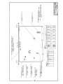
This chapter describes the circuitry of the board. A Block
Diagram of this board is shown in 4500-939.
1. Write 0BH to the Status Register:
Turns off the Red LED (Bit 0 = 1).
•
Turns on the Green LED (Bit 1 = 1).
•
Enables Interrupts (Bit 3 = 1).
•
2. Write the desired interrupt vector to the Vector Register.
3. Write 09H to the Board Control Register:
Selects Continuous Mode (Bit 0 = 1).
•
Allows Acquisition Complete Interrupts to occur (Bit 1 = 0).
•
Selects Software Trigger Type (Bit 2 = 0).
•
Enables Timed Periodic Triggering by enabling the
•
Conversion Timer (Bit 3 = 1).
4. Write 80H to the Scan Program Register:
Channel 0 (Bits 0-4 = 0).
•
Gain of 1 (Bits 5-6 = 0).
•
Single channel in the scan sequence (Bit 7 = 1).
•
5. Write 400H (1024) to the Conversion Count Register.
6. Program Conversion Timer for 100 microseconds:
a) Write 54H to the Counter Control Register.
b) Write 02H to the Timer Prescaler.
c) Write 94H to the Counter Control Register.
d) Write 64H (100) to the Conversion Timer.
7. Write any byte value to the Start Conversion Register to start the
acquisition.
The Software Trigger initiates the acquisition sequence by
causing an A/D conversion of channel 0. Thereafter the
Conversion Timer will cause A/D conversions of channel 0 every
100 microseconds. After filling each half of the Dual Port RAM,
the state of the Memory Bit (Bit 6 of the Board Status Register)
will change to indicate which half was most recently filled. This
bit could be periodically polled (possibly with a separate task) if
more than 63K samples of pre-trigger A/D data are desired.
32768 (32K) consecutive 16-bit data samples may then be read
from Dual Port RAM starting at the board's base address plus
20000H, if the Memory Bit is a "0" or starting at the board's base
address plus 30000H if the Memory Bit is a "1". The 12-bit A/D
data is left justified in each 16-bit sample.
8. Write any byte value to the Start Conversion Register to stop the
acquisition.
VMEbus INTERFACE
The VMEbus Interface is composed of four functional circuit
areas:
•
•
•
•
Address and data buffers (U41, U42, U55, U58, U59).
Bus control & address decoding (U57, U56, U40, U43,
U34, & U15).
Interrupter (U54, U53, U16).
DC-to-DC Converter (U39).
Bus Control Logic
Comparator U57 decodes the upper 6 address lines (A18-A23)
to see if they correspond to the base address jumper setting (J9).
U57 also makes sure that the VMEbus control lines IACK* and
LWORD* are valid. Programmable Logic Device (PLD) U56
determines if a valid VMEbus data transfer is occuring by monitoring
the output of the comparator, the state of the address modifiers
(AM0-AM5), the address modifier jumper setting (J10) and the
VMEbus data strobes (DS0* and DS1*). U56 also monitors a
control line from the VMEbus Interrupter (IVAL*) to determine if a
valid interrupt acknowledge cycle is occuring. The local control lines
produced by U56 will signal other logic circuits on the board that a
valid data bus transfer is occurring.
U56 also contains the local data bus arbitration circuit for the
Dual Port RAM. This circuit arbitrates the local data bus between a
VMEbus data transfer and the Acquisition Control Logic which
"writes" the A/D data into the Dual Port RAM.
VMEbus Interrupter Logic
PLD U53 inputs control lines which signal when to cause an
interrupt. If interrupts have been enabled and that type of interrupt
has been selected U53 will output an active interrupt pending signal
(IPEND*). The interrupt pending signal causes decoder U54 to drive
one of seven interrupt request lines low (IRQ1*-IRQ7*) depending
on the interrupt level selected by J7. Note that if all three positions of
J7 are open, corresponding to an interrupt level of "0", no interrupt
will be caused even though interrupts may be enabled.
The Software Trigger causes the board to operate in the Block
Mode. The board will now perform 1024 A/D conversions and then
stop, causing an interrupt.
The Interrupt Service Routine may then read 65536 (64K) 16-bit
data samples from Dual Port RAM, starting at the board's base
address plus 20000H, and separate the pre-trigger and post-trigger
data samples.
U53 also monitors the VMEbus interrupt acknowledge input
signal (IACKIN*) and drives the VMEbus interrupt acknowledge
output signal (IACKOUT*). When an active interrupt acknowledge
input occurs U53 first checks to see if the interrupt level of the
interrupt acknowledge (A1-A3) is the same as the interrupt level of
the board as selected by J7. If the interrupt levels match, and U53
has caused an interrupt, then U53 signals the Bus Control Logic that
a valid interrupt acknowledge cycle is occuring. The Vector Register
(U16) contains the interrupt vector which is read during an interrupt
acknowledge cycle. If the interrupt levels do not match, or U53 has
not caused an interrupt, then U53 drives the interrupt acknowledge
output (IACKOUT*) low, passing the interrupt acknowledge on to the
next card.
The last 1024 data samples have been stored sequentially in the
Dual Port RAM starting after the address pointed to by the PreTrigger Data Pointer. This address is found as follows:
a) Read Pre-Trigger-Data-Pointer (PTDP).
b) Multiply PTDP by 2.
c) Add the result from (b) to 20000H.
The address containing last Pre-Trigger Data equals the board's
base address plus 20000H + 2(PTDP).
- 17-
AVME9325 USER'S MANUAL
High Speed Analog Input Board With RAM
___________________________________________________________________________________________
DC-To-DC Converter
ANALOG INPUT SECTION
U39 is a hybrid, regulated DC-to-DC converter which provides
+15 volts and -15 volts from the +5 volt supply available on the
VMEbus through the P1 connector. The ±15 volt supplies are
required for the analog circuitry on the board. ±15 volt supplies are
used rather than the ±12 volt supplies available on the VMEbus to
accommodate the ±10 volt input span of the analog circuitry.
The various functional areas comprising the analog input
circuitry are described in the following subsections.
Analog Input Multiplexer
The Input configuration consists of four 8-input, CMOS analog
multiplexers (U48-51) and accepts 16 differential or 32 single-ended
inputs via the Analog Input Connector, P2. The three least
significant channel bits of the Scan Program Register are applied to
each of the 8-input multiplexers to determine which one of the eight
inputs will be activated. When configured for single-ended operation,
only one of the analog multiplexers is enabled at a time. For
differential operation, two analog multiplexers are enabled
simultaneously.
ON BOARD ADDRESSING
On-Board addresses are decoded through U43, U34 and U15.
The registers themselves are implemented as follows:
•
•
•
•
•
•
•
•
•
•
I.D. PROM (U17)
Board Status Register (U23, U24)
Interrupt Vector Register (U16)
Board Control Register (U12, U13)
Scan Program Register (U1, U2, U3)
Timer Prescaler, Conversion Timer & Counter Control (U4)
Conversion Counter (U11, U33)
Pre-Trigger Data Pointer (U14, U25)
Dual Port RAM (U18, U19, U20, U26, U27, U28, U29)
The Start Conversion Register is implemented only as an
address.
PLD U30 decodes the higher order channel bits from the Scan
Program Register and is jumper programmed for either differential or
single-ended operation via J2.
Jumper J8 is used to connect the outputs of the analog
multiplexers to the instrumentation amplifier (U52). In the differential
configuration, a pair of multiplexers is connected to the
instrumentation amplifier. In the single-ended configuration, each
multiplexer is connected to the '+' input of the instrumentation
amplifier and the SENSE input, which is the single-ended reference
for all 32 channels, is connected to the '-' input of the
instrumentation amplifier.
Scan Program Register
The Scan Program Register is configured as a 256 x 8-bit FIFO.
Writing Scan Codes to this register will increment the Scan Program
Memory Pointer (U1), a counter which drives the address lines of a
Static RAM IC (U2), allowing the next Scan Code to be written into
the following memory location. Writing a Scan Code with BIT 7 set
to a "1" will cause U46 to reset after that Scan Code has been
loaded. Once U1 has been reset the Static RAM will output the first
Scan Code written to the Scan Program Register. The Scan
Program Register is also reset at the end of a programmed
sequence of data acquisitions and on a board reset.
Instrumentation Amplifier
The instrumentation amplifier is made up of three op-amps,
which are part of a four high-speed op-amp IC (U52), four matched
resistors (R22, R23, R24, R25) and common mode adjust (R27).
The common mode rejection ratio is maximized when the ratio
R24/R22 is equal to the ratio R25/R23. The common mode adjust is
used to compensate for errors due to the tolerance of the resistors
used. The gain of the instrumentation amplifier is set by the ratio
R24/R22. The circuit has been designed for unity gain.
Once a sequence of Scan Codes have been written to the Scan
Program Register they will remain in the FIFO until they are
overwritten. Resetting the board will not reset the contents of the
FIFO, rather it will reset the counter to point to the first Scan Code
allowing the same Scan sequence to be repeated.
Programmable Gain Circuit
PLD U30 decodes the two gain bits from the Scan Program
Register into four control lines. These control lines are used to
enable one of four CMOS switches contained in U31. The switches
select one of four possible feedback voltages for the programmable
gain amplifier (U35). These voltages are generated by a matched
resistor set and provide the programmable gains of x1, x2, x4 and
x8.
Dual Port RAM
The Dual Port RAM is made up of four 32K x 8-bit Static RAM
IC's providing a total of 128K bytes of memory. Since the 12 bit A/D
data is stored in a 2 byte field, the Dual Port RAM will hold a
maximum of 64K data samples. Local data bus arbitration (U56)
provides the Dual Port architecture. This architecture may result in a
delay in the bus access time if the access occurs while the
Acquisition Controller is storing the latest sampled data into the Dual
Port RAM. A 16-bit counter (U18, U19, U20) drives the address
lines of the RAM IC's and is incremented by the Acquisition Control
Logic to store data sequentially in the Dual Port RAM beginning at
the starting location of Dual Port RAM in the board's address space.
After a reset or the end of a programmed sequence of data
acquisitions, data for the next sequence of data acquisitions will
again be stored beginning at the starting location of Dual Port RAM.
Sample and Hold Circuit
The Sample and Hold circuit consists of two sample and hold
devices (U36 and U37) which operate in parallel. The outputs of
sample and holds are connected together through CMOS switches
(U38) which are buffered from the A/D by the fourth high-speed opamp (U52). By operating two sample and hold devices in parallel,
the reacquisition delay typical of a single such device is eliminated.
This provides for an increase in the throughput rate of the board.
- 17-
AVME9325 USER'S MANUAL
High Speed Analog Input Board With RAM
___________________________________________________________________________________________
In this way the two 16-bit counters are cascaded to provide
variable time periods anywhere from 2 microseconds to over 35
minutes. The output of the second counter is used by the
Acquisition Control Logic to cause A/D conversions if Timed
Periodic Triggering has been enabled.
The hold task is alternated from one device to the other giving
each device ample time to reacquire the next channel before it is to
be converted. The control of the Sample and Hold circuit is
performed by the Acquisition Control logic.
Analog to Digital Converter
TRIGGER OUTPUT
The Analog to Digital (A/D) Converter (U32) consists of a 12-bit
Analog-to-Digital converter, a precision reference, a high speed
comparator, successive approximation register, converter control
circuitry, a clock and a digital interface. The A/D Converter used on
model AVME9325-5 (U32A) will perform an A/D conversion in 3
microseconds, and the A/D Converter used on model AVME9325-10
(U32B) will perform an A/D conversion in 8.5 microseconds.
The trigger output connection is made via BNC connector P4 at
the front panel. The trigger output signal is an active-low signal
which goes low on a conversion trigger. The pulse width of this
signal can vary depending on which type of triggering is being used.
The minimum low pulse width of 150 nanoseconds will occur with
External or Software Triggering. The maximum low pulse width will
occur with Timed Periodic Triggering. This pulse width is a function
of the count value in the Timer Prescaler and varies from 1
microsecond to 32.8 milliseconds.
ACQUISITION CONTROL LOGIC
The Acquisition Control Logic is responsible for controlling the
operation of a user programmed sequence of data acquisitions.
This programming consists of the following:
•
•
•
•
•
5.0 SERVICE AND REPAIR
Setting up the board for interrupts if desired.
Setting up the programmable timer for timed periodic
conversions if desired.
Selecting the desired mode and type of triggering.
Writing the Scan Code(s) to the Scan Program Register.
Writing the desired number of conversions to the
Conversion Counter if Block Mode or Post-Trigger
Acquisition is desired.
This section provides calibration procedures, service diagrams
and instructions on how to obtain service and repair assistance.
SERVICE AND REPAIR ASSISTANCE
It is highly recommended that a non-functioning board be
returned to Acromag for repair. Acromag uses tested and burned-in
parts, and in some cases, parts that have been selected for
characteristics beyond that specified by the manufacturer. Acromag
has automated test equipment that thoroughly checks the
performance of each board. When a board is first produced and
when any repair is made, it is tested, placed in a burn-in room at
elevated temperature, and retested before shipment.
Once the board has been programmed, the Acquisition Control
Logic performs the following:
•
•
•
•
•
•
•
Control of the Sample and Hold Circuit.
Control of the A/D Converter.
Increments the Scan Program Memory Pointer after each
conversion.
Sets appropriate status bits in the Status Register.
Writes data into Dual Port RAM.
Sends a local Interrupt Request to the Interrupter.
Stops data acquisition when the count in the conversion
counter reaches zero.
Please refer to Acromag's Service Policy Bulletin or contact
Acromag for complete details on how to obtain parts and repair.
PRELIMINARY SERVICE PROCEDURE
Before beginning calibration or repair, be sure that all of the
procedures in Section 2, Preparation For Use, Have been followed.
The procedures are necessary since the board has switches and
jumpers that must be properly configured.
EXTERNAL TRIGGER
The External Trigger connection is made via BNC connector P3
at the front panel. The falling edge of the External Trigger input
triggers a mono-stable multivibrator (U21). U21 outputs a short
pulse on the falling edge of the External Trigger which is used by the
Acquisition Control Logic to start an A/D conversion. Once the
External Trigger signal has been driven low it should remain low for
at least 100 nanoseconds. The signal must return high for a
minimum of 100 nanoseconds before going low again.
NOTE: It has been observed that on occasion a "boot" program for
a disk operating system will "hang" waiting for the VMEbus
SYSFAIL* signal to be released by an intelligent disk controller
board. Acromag's non-intelligent slave boards assert the SYSFAIL*
signal as described in the VMEbus Specification Rev.C.1 and,
therefore, the disk operating system will remain "hung". The best
solution to this process is to correct the boot program so that it is no
longer dependent upon the SYSFAIL* signal. When this solution is
not practical, it is possible to disconnect the SYSFAIL* signal from
the circuitry on the Acromag board by cutting a PC board foil
between the two pads for J11. Caution should be exercised so as
not to cut any other foils nor to damage the board in any other way.
Call Acromag's Applications Engineering Department for assistance.
TIMED PERIODIC TRIGGER CIRCUIT
Timed Periodic Triggering is provided by two 16-bit
programmable counters within U4. A binary counter (U46) divides
the 16MHz system clock available on the VMEbus (SYSCLK*) down
to a 2MHz clock, which is used to clock the first counter (Timer
Prescaler). The output of the first counter is then used to clock the
second counter (Conversion Timer).
CAUTION: POWER MUST BE TURNED OFF BEFORE
REMOVING OR INSERTING BOARDS
- 17-
AVME9325 USER'S MANUAL
High Speed Analog Input Board With RAM
___________________________________________________________________________________________
1. Configure the board for differential inputs.
2. Connect the DVM signal and ground leads to pins 1 and 2
respectively of test point 2 (TP2).
3. Apply 0V to channel 0.
4. Setup the board so that channel 0 and gain of 8 are selected
(write E0H to Scan Program Register).
5. Adjust R20 until the voltage at TP2 is 0V (within 25uV).
CALIBRATION PROCEDURES
The analog input is calibrated at the factory for +/-10V bipolar
analog inputs. Should another input range be desired or should
recalibration ever become necessary, the board may be calibrated in
the field or may be returned to the factory for calibration. Care
should be taken to insure the integrity of any adjustments being
made. Refer to 4500-938 for Parts Location and Schematic
Drawings.
Sample And Hold Offset Calibration
The dual sample and hold circuit must be calibrated in order to
match the offsets of the two sample and hold devices. The sample
and hold offset calibration is performed as follows:
The following equipment will be required in order to calibrate the
analog input:
•
•
•
•
A frequency generator capable of +/-10V of output.
An oscilloscope.
A precision adjustable voltage source with 0 to 10V output
range, 0.001% accuracy and isolated output.
A precision Digital Voltmeter (DVM) with 0.001% accuracy
and isolated input.
1. Configure the board for the +/-10V bipolar configuration,
differential inputs, and bipolar two's complement data format
(See Section 2 for details).
2. Connect the precision voltage source to channel 0 and connect
the voltage source signal ground to analog common on the
board. These connections can be made at P2 or on a
termination panel if one is available.
3. Setup the board so that channel 0 and gain of 1 are selected
(write 80H to Scan Program Register).
4. Apply 0V to channel 0.
5. Adjust R21 until the data corresponding to the first sample and
hold (U36) matches the data corresponding to the second
sample and hold (U37).
6. Verify the calibration by applying a DC input equivalent to 1/2
LSB above 0V (i.e. : +0.0024 volts) and repeating step 5.
Note that the calibration of the analog input must be performed
in the following order:
1.
2.
3.
4.
Instrumentation Amplifier Calibration
Programmable Gain Stage Offset Calibration
Sample And Hold Offset Calibration
A/D Converter Calibration
If the board is calibrated for one input range and a different input
range is desired, then only the A/D Converter Calibration for the new
input range is necessary.
±10V Bipolar Calibration
Instrumentation Amplifier Calibration
Perform this Calibration as follows:
The instrumentation amplifier must be calibrated before any
other stage can be calibrated. The common mode adjustment (R27)
is used to precisely match the resistance in the instrumentation
amplifier so that differential inputs are accurately converted to singleended signals. The common mode rejection calibration is performed
as follows:
1. Configure the board for the +/-10V bipolar configuration,
differential inputs, and bipolar two's complement data format
(See Section 2 for details).
2. Connect the precision voltage source to channel 0 and connect
the voltage source signal ground to analog common on the
board. These connections can be made at P2 or on a
termination panel if one is available.
3. Setup the board so that channel 0 and gain of 1 are selected
(write 80H to Scan Program Register).
4. Apply a DC input voltage equivalent to 1/2 LSB above -10V (9.9976V). Assuming bipolar two's complement data format,
adjust R9 until data read on channel 0 toggles evenly between
8000 and 8010 (remember that the 12-bit data is left justified in
memory).
5. Apply a DC input voltage equivalent to 1 and 1/2 LSB less than
10V (+9.9927V). Assuming bipolar two's complement data
format, adjust R10 until data read on channel 0 toggles evenly
between 7FE0H and 7FF0H (remember that the 12-bit data is
left justified in memory).
1. Configure the board for differential inputs.
2. Connect the oscilloscope's signal and ground leads to pins 1
and 2, respectively, of test point 2 (TP2).
3. Setup the frequency generator for a +/-10V square wave output
at 60 Hz.
4. Connect the frequency generator's signal lead to the plus and
minus input of channel 0 and connect the ground lead to analog
common on the Board.
5. Setup the board so that channel number 0 and gain of 8 are
selected (write E0H to Scan Program Register).
6. Adjust R27 for the minimum AC signal at TP2.
Input Offset Calibration For The Programmable Gain Stage
The offset calibration for the programmable gain stage must
always be performed before calibration of the following stages. The
input offset must be nulled separately so that offset errors prior to
the programmable gain stage are not multiplied by that gain. The
offset calibration is performed as follows:
- 17-
AVME9325 USER'S MANUAL
High Speed Analog Input Board With RAM
___________________________________________________________________________________________
±5V Bipolar Calibration
Table 5.1: Replacement Parts
ACROMAG
REFERENCE
PART NO.
U1
1033-710
U2
1033-471
U3,12,20,24,42
1033-273
U4
1033-671
U5,6,14,16,25,41
1033-283
U7
5016-574
U8
5016-575
U9,45
1033-255
U10
1033-253
U11,33
1033-708
U13
1033-670
U15
5016-576
U18,19
1033-707
U21,22
1033-276
U23
1033-657
U26-29
1033-410
U30
5016-577
U31,38
1033-705
U34
5016-578
U35
1033-725
U36
1033-677
U39
4001-035
U40
1033-709
U43
5016-579
U44
1033-623
U46
1033-284
U47
1033-658
U48
1033-292
U52
1033-726
U53
5016-580
U54
1033-048
U55
1033-728
U56
5016-581
U57
1033-626
U58,59
1033-627
Perform this Calibration as follows:
1. Configure the board for the ±5V bipolar configuration, differential
inputs, and bipolar two's complement data format (See Section 2
for details).
2. Connect the precision voltage source to channel 0 and connect
the voltage source signal ground to analog common on the
Board. These connections can be made at P2 or on a
termination panel if one is available.
3. Setup the board so that channel 0 and gain of 1 are selected
(write 80H to Scan Program Register).
4. Apply a DC input voltage equivalent to 1/2 LSB above -5V
(-4.9988V). Assuming bipolar two's complement data format,
adjust R9 until data read on channel 0 toggles evenly between
8000H and 8010H (remember that the 12-bit data is left justified
in memory).
5. Apply a DC input voltage equivalent to 1 and 1/2 LSB less than
5V (+4.9963V). Assuming bipolar two's complement data
format, adjust R10 until data read on channel 0 toggles evenly
between 7FE0H and 7FF0H (remember that the 12-bit data is
left justified in memory).
Unipolar Calibration
Perform this Calibration as follows:
1. Configure the board for the 0 to 10V unipolar configuration,
differential inputs, and unipolar straight binary data format (See
Section 2 for details).
2. Connect the precision voltage source to channel 0 and connect
the voltage source signal ground to analog common on the
board. These connections can be made at P2 or on a
termination panel if one is available.
3. Setup the board so that channel 0 and gain of 1 are selected
(write 80H to Scan Program Register).
4. Apply a DC input voltage equivalent to 1/2 LSB above 0V
(+0.0012V). Assuming unipolar straight binary data format,
adjust R11 until data read on channel 0 toggles evenly between
0000 and 0010 (remember that the 12-bit data is left justified in
memory).
5. Apply a DC input voltage equivalent to 1 and 1/2 LSB less than
10V (+9.9963V). Assuming unipolar straight binary data format,
adjust R10 until data read on channel 0 toggles evenly between
FFE0H and FFF0H (remember that the 12-bit data is left
justified in memory).
REPLACEABLE PARTS
The Replaceable Parts List (Table 5.1) is provided as an aid to
the user in troubleshooting the board. Replacement parts and repair
services are available from Acromag. If parts are replaced in the
analog circuitry, recalibration may be required. If repair is deemed
necessary in this circuitry, it is highly recommended that the board
be returned to Acromag for repair and recalibration.
Changes are sometimes made to improve the product, to
facilitate delivery, or to control cost. It is therefore important to
include the reference Number, the Acromag Part Number, the Board
Model Number, and the Board Serial Number when providing
information to order parts.
- 17-
DESCRIPTION
74F579
TMM2015AP-15
74LS244
8254-5
74LS373
PLS153
PLS153
74LS04
74LS02
74F779
74LS174
PLS153
74LS590
74LS423
74LS175
HM62256LP-12
PLS153
HI-201HS-7
PLS173
OPA602AP
SCH5320KH
DC - DC CONVERTER
74LS33
PLS173
74F38
74LS393
74LS164
HI-508A-7
OPA404KP
PLS153
7445
74F373
PLS153
AM25LS2521
74LS645-1ND
R1,3
R4
R5
R9, 10
R15,14,13,12
1006-760
1006-789
1100-268
1100-139
1100-522
R16-19
R20
R21
(R22,24), (R23,25)
R27
R28, 29
R30
R31
1006-741
1100-149
1100-145
1100-262
1100-138
1006-693
1100-494
1000-834
4.99K
10K
9 X 4.7K NETWORK
100 OHM POT
MATCHED SET (4K, 2K,
1K, & 1K, respectively)
3.16K
100K POT
10K POT
MATCHED PAIRS, 10K
50 OHM POT
1K
7 X 1K NETWORK
1.8K
L1-L9
1016-005
47 UHF INDUCTOR
D1
D2
D3-10
1001-165
1001-166
1001-113
GREEN LED
RED LED
DIODE 1N914B
AVME9325 USER'S MANUAL
High Speed Analog Input Board With RAM
___________________________________________________________________________________________
Replacement Parts Continued...
ACROMAG
REFERENCE
PART NO.
C1-23,26-34,38-40,
C43,44,46-55,
1002-530
C57-70, 75-81
C24,37
1002-545
C35,42,45,72,73,
1002-321
C84,85,87,88
C36,56
1002-549
C71,74
1002-422
C82,83
1002-313
DESCRIPTION
0.1uF CAP
22pF CAP
10uF CAP
100pF CAP
33pF CAP
68uF CAP
TP1, J1, J3, J4.
J8
J7
TP2, J2, J10-11
J9
J6
1004-333
1004-365
1004-374
1004-410
1004-383
1004-411
1 X 3 POS.
1 X 4 POS.
2 X 6 POS.
1 X 2 POS.
2 X 12 POS.
2 X 4 POS.
P1
P2
P3, 4
1004-505
1004-528
1004-529
96 POS CONNECTOR
64 POS. CONNECTOR
BCN CON.
Model AVME9325-5 Special Parts
U17
5016-582
U32A
1033-703
ANALOG INPUT SECTION
Input type............................................
Input configuration..............................
Input range.........................................
Programmable gain.............................
Input overvoltage protection................
Input resistance..................................
Input bias current................................
Common Mode Rejection Ratio..........
Channel to Channel Rejection Ratio...
RFI resistance @27MHz, 151 MHz,
and 467 MHz......................................
Settling time: (to 0.01% of 20V step):
AVME9325-5.................................
AVME9325-10...............................
A/D conversion time:
AVME9325-5.................................
AVME9325-10...............................
A/D resolution.....................................
No missing codes over temperature...
A/D nonlinearity..................................
System Accuracy................................
Overall throughput rate:
AVME9325-5.................................
TBP18S030
AD578LN
R2
R6, 26
R7
R11
1006-793
1006-685
1100-334
1100-145
11K
825 OHMS
0 OHMS
10K POT
C25
C41
C86
1002-549
1002-321
1002-545
100 pF CAP
10 uF CAP
22pF CAP
J5
1004-410
1 X 2 POS.
Model AVME9325-10 Special Parts
U17
5016-583
U32B
1033-673
Mating connectors:
P1..................................................
P2..................................................
P3, P4............................................
Power requirements:
+ 5 Volts +0.25/-0.125...................
+ 12 Volts......................................
- 12Volts........................................
VMEbus Access:
Time (Typical, Measured from
the falling edge of Dsx* to the
falling edge of DTACK*)................
If A/D conversion
(Dual Port RAM Arbitration)
is in progress.................................
TBP18S030
HI1-774K
R2
R7
R8
R11
1006-760
1006-597
1006-885
1100-149
4.99K
100 OHMS
100K
100K POT
C25
C86
1002-545
1002-422
22pF CAP
33pF CAP
AVME9325-10...............................
Gain temperature coefficient...............
Offset temperature coefficient............
6.0 SPECIFICATIONS
GENERAL SPECIFICATIONS
Operating temperature........................
Storage temperature...........................
Physical Characteristics:
Length............................................
Width.............................................
Board thickness.............................
Component height..........................
Recommended card spacing..............
0 to +70° C
-25 to +85°C
9.187 in. (233.3 mm)
6.299 in. (160 mm)
0.062. in. (1.59 mm)
0.55 in. (13.97 mm)
0.8 in. (20.32 mm)
- 17-
96 pin 603-2-IEC class 2
64 pin 603-2-IEC class 2
BNC jack
3.0 Amps Typical
No load
No load
370 nS typical
700nS Max
Non-isolated voltage
16 differential or 32 singleended
±5, ±10 Volts bipolar or 0
to 10 Volts unipolar
x1, x2, x4, x8
32 Volts continuous
5,000 Megohms
150pA typical
90db, Typical, 60Hz
90db, Typical, 60Hz
< 0.25% of FSR at 10V/m
field intensity
4us typical
7us typical
3us max.
9us max.
12 bits
12 bits
±1/2 LSB
0.04% of FSR
200,000 conversions per
second (5us/conversion)
100,000 conversions per
second (10us/conversion)
±50 ppm/°C Max
±24 ppm/°C Max