1
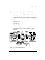
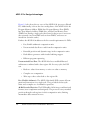
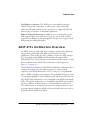
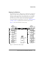
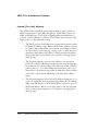
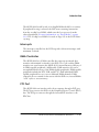
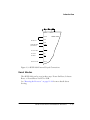
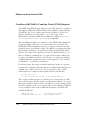
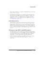
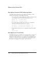
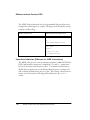
1 INTRODUCTION
Figure 1-0.
Table 1-0.
Listing 1-0.
Purpose
The ADSP-219x/2192 DSP Hardware Reference provides architectural
information on the ADSP-219x modified Harvard architecture Digital
Signal Processor (DSP) core and ADSP-2192 DSP product. The architectural descriptions cover functional blocks, buses, and ports, including all
features and processes they support. For programming information, see
the ADSP-219x DSP Instruction Set Reference.
Audience
DSP system designers and programmers who are familiar with signal processing concepts are the primary audience for this manual. This manual
assumes that the audience has a working knowledge of microcomputer
technology and DSP-related mathematics.
DSP system designers and programmers who are unfamiliar with signal
processing can use this manual, but they should supplement this manual
with other texts that describe DSP techniques.
All readers, particularly system designers, should refer to the DSP’s data
sheet for timing, electrical, and package specifications. For additional suggested reading, see “For More Information About Analog Products” on
page 1-23.
ADSP-219x/2192 DSP Hardware Reference
1-1
Overview—Why Fixed-Point DSP?
Overview—Why Fixed-Point DSP?
A digital signal processor’s data format determines its ability to handle signals of differing precision, dynamic range, and signal-to-noise ratios.
Because 16-bit, fixed-point DSP math is required for certain DSP coding
algorithms, using a 16-bit, fixed-point DSP can provide all the features
needed for certain algorithm and software development efforts. Also, a
narrower bus width (16-bit as opposed to 32- or 64-bit wide) leads to
reduced power consumption and other design savings. The extent to
which this is true depends on the fixed-point processor’s architecture.
High-level language programmability, large address spaces, and wide
dynamic range allow system development time to be spent on algorithms
and signal processing concerns, rather than assembly language coding,
code paging, and error handling. The ADSP-2192 DSP is a highly integrated, 16-bit fixed-point DSP that provides many of these design
advantages.
ADSP-219x Design Advantages
The ADSP-219x family DSPs are high-performance 16-bit DSPs for communications, instrumentation, industrial/control, voice/speech, medical,
military, and other applications. These DSPs provide a DSP core that is
compatible with previous ADSP-2100 family DSPs, but they also provide
many additional features. The ADSP-219x core combines with on-chip
peripherals to form a complete system-on-a-chip. The off-core peripherals
add on-chip SRAM, integrated I/O peripherals, timer, and interrupt
controller.
The ADSP-219x architecture balances a high performance processor core
with high performance buses (PM, DM, DMA). In the core, every computational instruction can execute in a single cycle. The buses and
instruction cache provide rapid, unimpeded data flow to the core to maintain the execution rate.
1-2
ADSP-219x/2192 DSP Hardware Reference
Introduction
Figure 1-1 shows a detailed block diagram of the ADSP-2192 processor,
illustrating the following architectural features:
• Computation units for the ADSP-219x family—multiplier, ALU,
shifter, and data register file
• Program sequencer for the ADSP-219x family, with related instruction cache, interval timer, and Data Address Generators (DAG1 and
DAG2)
• PCI/USB Host port
• AC’97 codec port
• SRAM for the ADSP-2192
• Input/Output (I/O) processor with integrated DMA controllers
• JTAG Test Access Port for board test and emulation on the
ADSP-2192
ⴛ ⴛ ⴛ ⴛ ⴛ #$
%
!"
&
Figure 1-1. ADSP-2192 Block Diagram
ADSP-219x/2192 DSP Hardware Reference
1-3
ADSP-219x Design Advantages
Figure 1-1 also shows the two cores of the ADSP-2192 (processors P0 and
P1). Additionally, it shows the four on-chip buses of the ADSP-2192: the
Program Memory Address (PMA) bus, Program Memory Data (PMD)
bus, Data Memory Address (DMA) bus, and the Data Memory Data
(DMD) bus. During a single cycle, these buses let the processor access two
data operands (one from PMD and one from DMD), and access an
instruction (from the cache).
Further, the ADSP-219x addresses the five central requirements for DSPs:
• Fast, flexible arithmetic computation units
• Unconstrained data flow to and from the computation units
• Extended precision and dynamic range in the computation units
• Dual address generators with circular buffering support
• Efficient program sequencing
Unconstrained Data Flow. The ADSP-219x has a modified Harvard
architecture combined with a data register file. In every cycle, the DSP
can:
• Read two values from memory or write one value to memory
• Complete one computation
• Write up to three values back to the register file
Fast, Flexible Arithmetic. The ADSP-219x family DSPs execute all computational instructions in a single cycle. They provide both fast cycle
times and a complete set of arithmetic operations.
40-Bit Extended Precision. The DSP handles 16-bit integer and fractional
formats (twos-complement and unsigned). The processors carry extended
precision through result registers in their computation units, limiting
intermediate data truncation errors.
1-4
ADSP-219x/2192 DSP Hardware Reference
Introduction
Dual Address Generators. The DSP has two data address generators
(DAGs) that provide immediate or indirect (pre- and post-modify)
addressing. Modulus and bit-reverse operations are supported with only
memory page constraints on data buffer placement.
Efficient Program Sequencing. In addition to zero-overhead loops, the
DSP supports quick setup and exit for loops. Loops are both nestable
(eight levels in hardware) and interruptable. The processors support both
delayed and non-delayed branches.
ADSP-219x Architecture Overview
An ADSP-219x is a single-chip microcomputer optimized for digital signal processing (DSP) and other high speed numeric processing
applications. These DSPs provide a complete system-on-a-chip, integrating a large, high-speed SRAM and I/O peripherals supported by a
dedicated I/O bus. The following sections summarize the features of each
functional block in the ADSP-219x architecture, which appears in
Figure 1-1 on page 1-3.
The ADSP-2192 combines the ADSP-219x family base architecture (three
computational units, two data address generators, and a program
sequencer) with PCI/USB interface, AC’97 serial port, a programmable
timer, a DMA controller, general purpose Programmable Flag pins, extensive interrupt capabilities, and on-chip program and data memory blocks.
The ADSP-2192 architecture is code compatible with ADSP-218x family
DSPs. Though the architectures are compatible, the ADSP-2192 architecture has a number of enhancements over the ADSP-218x architecture.
The enhancements to computational units, data address generators, and
program sequencer make the ADSP-2192 more flexible and even easier to
program than the ADSP-218x DSPs.
ADSP-219x/2192 DSP Hardware Reference
1-5
ADSP-219x Architecture Overview
Indirect addressing options provide addressing flexibility—pre-modify
with no update, pre- and post-modify by an immediate 8-bit, two’s-complement value and base address registers for easier implementation of
circular buffering.
The ADSP-2192 integrates 128K words of on-chip memory configured as
32K words (24-bit) of program RAM (16K words each on DSP P0 and
DSP P1) and 96K words (16-bit) of data RAM (64K words on DSP P0
and 32K words on DSP P1). Power-down circuitry is also provided to
meet the low power needs of battery operated portable equipment.
The ADSP-2192’s flexible architecture and comprehensive instruction set
support multiple operations in parallel. For example, in one processor
cycle, each core of the ADSP-2192 can:
• Generate an address for the next instruction fetch
• Fetch the next instruction
• Perform one or two data moves
• Update one or two data address pointers
• Perform a computational operation
DSP Core Architecture
The ADSP-219x instruction set provides flexible data moves and multifunction (one or two data moves with a computation) instructions. Every
single-word instruction can be executed in a single processor cycle. The
ADSP-219x assembly language uses an algebraic syntax for ease of coding
and readability. A comprehensive set of development tools supports program development.
Figure 1-1 on page 1-3 shows the architecture of the ADSP-219x core. It
contains three independent computational units: the ALU, the multiplier/accumulator, and the shifter.
1-6
ADSP-219x/2192 DSP Hardware Reference
Introduction
The computational units process 16-bit data from the register file and
have provisions to support multiprecision computations. The ALU performs a standard set of arithmetic and logic operations; division primitives
also are supported. The multiplier performs single-cycle multiply, multiply/add, and multiply/subtract operations. The multiplier now has two
40-bit accumulator results. The shifter performs logical and arithmetic
shifts, normalization, denormalization, and derive exponent operations.
The shifter can efficiently implement numeric format control, including
multiword and block floating-point representations.
Register-usage rules influence placement of input and results within the
computational units. For all unconditional, non-multi-function instructions, the computational units’ data registers act as a data register file,
permitting any input or result register to provide input to any unit for a
computation. For feedback operations, the computational units let the
output (result) of any unit be input to any unit on the next cycle. For conditional or multifunction instructions, there are restrictions limiting
which data registers may provide inputs or receive results from each computational unit. For more information, see “Multifunction
Computations” on page 2-60.
A powerful program sequencer controls the flow of instruction execution.
The sequencer supports conditional jumps, subroutine calls, and low
interrupt overhead. With internal loop counters and loop stacks, the
ADSP-2192 executes looped code with zero overhead; no explicit jump
instructions are required to maintain loops.
Two data address generators (DAGs) provide addresses for simultaneous
dual operand fetches (from data memory and program memory). Each
DAG maintains and updates four 16-bit address pointers. Whenever the
pointer is used to access data (indirect addressing), it is pre- or post-modified by the value of one of four possible modify registers. A length value
and base address may be associated with each pointer to implement automatic modulo addressing for circular buffers.
ADSP-219x/2192 DSP Hardware Reference
1-7
ADSP-219x Architecture Overview
Page registers in the DAGs allow circular addressing within 64K word
boundaries of each of the 256 memory pages, but these buffers may not
cross page boundaries. Secondary registers duplicate all the primary registers in the DAGs; switching between primary and secondary registers
provides a fast context switch.
Efficient data transfer in the core is achieved by using internal buses:
• Program Memory Address (PMA) Bus
• Program Memory Data (PMD) Bus
• Data Memory Address (DMA) Bus
• Data Memory Data (DMD) Bus
• IO or DMA Address Bus
• IO or DMA Data Bus
Program memory can store both instructions and data, permitting the
ADSP-219x to fetch two operands in a single cycle, one from program
memory and one from data memory. The DSP’s dual memory buses also
let the ADSP-219x core fetch an operand from data memory and the next
instruction from program memory in a single cycle.
DSP Peripherals Architecture
Figure 1-1 on page 1-3 shows the DSP’s on-chip peripherals, as part of a
typical ADSP-2192 system with peripheral connections.The ADSP-2192
has a 16-bit PCI/USB host port. This port provides either PCI or USB
functionality via the Peripheral Device Control (PDC) bus.
The ADSP-2192 can respond to up to thirteen interrupts, using a priority
scheme implemented by the interrupt controller.
1-8
ADSP-219x/2192 DSP Hardware Reference
Introduction
Memory Architecture
The ADSP-2192 integrates 128K words of on-chip memory configured as
32K words (24-bit) of program RAM (16K words each on DSP P0 and
DSP P1) and 96K words (16-bit) of data RAM (64K words on DSP P0
and 32K words on DSP P1). Power-down circuitry is also provided to
meet the low power needs of battery operated portable equipment.
For more information on these blocks, see the section “ADSP-2192 Memory Map” on page 5-8, which discusses the memory map in detail.
Figure 1-2 shows the ADSP-2192’s memory map.
Figure 1-2. ADSP-2192 Memory Maps
ADSP-219x/2192 DSP Hardware Reference
1-9
ADSP-219x Architecture Overview
Internal (On-chip) Memory
The ADSP-2192’s unified program and data memory space consists of
16M locations that are accessible through two 24-bit address buses, the
PMA and DMA buses. The DSP uses slightly different mechanisms to
generate a 24-bit address for each bus. The DSP has three functions that
support access to the full memory map.
• The DAGs generate 24-bit addresses for data fetches from the entire
DSP memory address range. Because DAG index (address) registers
are 16 bits wide and hold the lower 16-bits of the address, each of
the DAGs has its own 8-bit page register (DMPGx) to hold the most
significant eight address bits. Before a DAG generates an address,
the program must set the DAG’s DMPGx register to the appropriate
memory page.
• The Program Sequencer generates the addresses for instruction
fetches. For relative addressing instructions, the program sequencer
bases addresses for relative jumps, calls, and loops on the 24-bit Program Counter (PC). For direct addressing instructions (two-word
instructions), the instruction provides an immediate 24-bit address
value. The PC allows linear addressing of the full 24 bit address
range.
• The Program Sequencer relies on an 8-bit Indirect Jump page (IJPG)
register to supply the most significant eight address bits for indirect
jumps and calls that use a 16-bit DAG address register for part of
the branch address. Before a cross page jump or call, the program
must set the program sequencer’s IJPG register to the appropriate
memory page.
1-10
ADSP-219x/2192 DSP Hardware Reference
Introduction
The ADSP-2192 has 4K words of on-chip ROM that holds boot routines.
If peripheral booting is selected, the DSP starts executing instructions
from the on-chip boot ROM, which starts the boot process from the
selected peripheral. For more information, see “Reset Modes” on page
1-13. The on-chip boot ROM is located on Page 255 in the DSP’s memory map.
Interrupts
The interrupt controller lets the DSP respond to thirteen interrupts with
minimum overhead.
DMA Controller
The ADSP-2192 has a DMA controller that supports automated data
transfers with minimal overhead for the DSP core. Cycle stealing DMA
transfers can occur between the ADSP-2192’s internal memory and any of
its DMA capable peripherals. Additionally, DMA transfers also can be
accomplished between any of the DMA capable peripherals. DMA capable
peripherals include the PCI, USB, and AC’97. Each individual DMA
capable peripheral has one or more dedicated DMA channels. DMA
sequences do not contend for bus access with the DSP core, instead DMAs
“steal” cycles to access memory.
PCI Port
The ADSP-2192 can interface with a host computer through a PCI port.
The PCI port accesses the DSPs via the Peripheral Device Control (PDC)
bus. The PCI port connects through the internal PCI interface to the
PDC bus.
ADSP-219x/2192 DSP Hardware Reference
1-11
ADSP-219x Architecture Overview
USB Port
The ADSP-2192 can interface with a host computer through a USB port.
The USB port accesses the DSPs via the Peripheral Device Control (PDC)
bus. The USB port connects through the internal USB interface to the
PDC bus.
AC’97 Interface
The ADSP-2192 includes an AC’97 interface that complies with the
AC’97 specification. The AC’97 interface connects the host’s Digital Controller (DC) chip set and between one and four analog codecs.
Low Power Operation
All pins on the ADSP-2192 remain active as long as power is maintained
to the chip. This chip does not have a specifically-defined powerdown
state; at any time either or both of the two processors can be in a low
power state, and any or all of the interfaces can be in a low power state.
Additionally, each peripheral interface (USB, PCI, and AC’97) can be put
into a low power mode, as described in “System Design” on page 11-1.
Clock Signals
The ADSP-2192 can be clocked by a crystal oscillator. If a crystal oscillator is used, the crystal should be connected across the XTALI/O pins, with
two capacitors connected as shown in Figure 1-3 on page 1-13. Capacitor
values are dependent on crystal type and should be specified by the crystal
manufacturer. A parallel-resonant, fundamental frequency, microprocessor-grade 24.576 MHz crystal should be used for this configuration.
1-12
ADSP-219x/2192 DSP Hardware Reference
Introduction
ADSP-2192
Figure 1-3. ADSP-2192 External Crystal Connections
Reset Modes
The ADSP-2192 can be reset in three ways: Power On Reset, Software
Reset, or Forced Reset Via PCI or USB.
See “Resetting the Processor” on page 11-14 for more details about
booting.
ADSP-219x/2192 DSP Hardware Reference
1-13
Development Tools
JTAG Port
The ADSP-2192 includes a JTAG port. Emulators use the JTAG port to
monitor and control the DSP during emulation. Emulators using this port
provide full-speed emulation with access to inspect and modify memory,
registers, and processor stacks. JTAG-based emulation is non-intrusive
and does not affect target system loading or timing. Note that the
ADSP-2192 JTAG does not support boundary scan.
Development Tools
The ADSP-219x is supported by VisualDSP++, an easy-to-use project
management environment, comprised of an Integrated Development and
Debugging Environment (IDDE). VisualDSP++ lets you manage projects
from start to finish from within a single, integrated interface. Because the
project development and debug environments are integrated, you can
move easily between editing, building, and debugging activities.
Flexible Project Management. The IDDE provides flexible project management for the development of DSP applications. It provides you with
access to all the activities necessary to create and debug DSP projects. You
can create or modify source files or view listing or map files with the
IDDE Editor. This powerful Editor includes multiple language syntax
highlighting, OLE drag and drop, bookmarks, and standard editing operations such as undo/redo, find/replace, copy/paste/cut, and go to.
VisualDSP++ includes access to the DSP C/C++ Compiler, C Run-time
Library, Assembler, Linker, Loader, Splitter, and Simulator. You specify
options for these Tools through property page dialog boxes. These options
control how the tools process inputs and generate outputs, and the
options have a one-to-one correspondence to the tools’ command-line
switches. You can define these options once or modify them to meet
changing development needs. You also can access the Tools from the operating system command line if you choose.
1-14
ADSP-219x/2192 DSP Hardware Reference
Introduction
Greatly Reduced Debugging Time. VisualDSP++ has an easy-to-use,
common interface for all processor simulators and emulators available
through Analog Devices and third parties or custom developments. It has
many features that greatly reduce debugging time. You can view C source
interspersed with the resulting Assembly code. You can profile execution
of a range of instructions in a program; set simulated watch points on
hardware and software registers, program and data memory; and trace
instruction execution and memory accesses.
These features enable you to correct coding errors, identify bottlenecks,
and examine DSP performance. You can select any combination of registers to view in a single customizable window. VisualDSP++ can also
generate inputs, outputs, and interrupts, so you can simulate real-world
application conditions.
Software Development Tools. Software development tools, which support
the ADSP-219x family, let you develop applications that take full advantage of the DSP architecture, including shared memory and memory
overlays. Software development tools include the C/C++ Compiler,
C Run-time Library, DSP and Math Libraries, Assembler, Linker, Loader,
Splitter, and Simulator.
C/C++ Compiler & Assembler. The C/C++ Compiler generates efficient
code that is optimized for both code density and execution time. The
C/C++ Compiler allows you to include Assembly language statements
inline. Because of this, you can program in C/C++ and still use Assembly
for time-critical loops.
You can also use pretested Math, DSP, and C Run-time Library routines
to help shorten your time to market. The ADSP-219x family assembly
language is based on an algebraic syntax that is easy to learn, program, and
debug.
ADSP-219x/2192 DSP Hardware Reference
1-15
Differences from Previous DSPs
Linker & Loader. The Linker provides flexible system definition through
Linker Description Files (.LDF). In a single LDF, you can define different
types of executables for a single processor or multiprocessor system. The
Linker resolves symbols over multiple executables, maximizes memory use,
and easily shares common code among multiple processors. The Loader
allows multiprocessor system configuration with smaller code and faster
boot time.
Differences from Previous DSPs
This section identifies differences between the ADSP-219x DSPs and previous ADSP-2100 family DSPs: ADSP-210x, ADSP-211x, ADSP-217x,
and ADSP-218x. The ADSP-219x preserves much of the core ADSP-2100
family architecture, while extending performance and functionality. For
background information on previous ADSP-2100 family DSPs, see the
ADSP-2100 Family User’s Manual. For background information on the
ADSP-218x family DSPs, see the ADSP-218x DSP Hardware Reference.
The sections that follow describe key differences and enhancements of the
ADSP-219x over previous ADSP-2100 family DSPs. These enhancements
also lead to some differences in the instruction sets between DSP families.
For more information, see the ADSP-219x DSP Instruction Set Reference.
Computational Units and Data Register File
The ADSP-219x DSP’s computational units differ from those of the
ADSP-218x’s, because the ADSP-219x data registers act as a register file
for unconditional, single-function instructions. In these instructions, any
data register may be an input to any computational unit. For conditional
and/or multifunction instructions, the ADSP-219x and ADSP-218x DSP
families have the same data register usage restrictions — AX and AY for
ALU, MX and MY for the multiplier, and SI for shifter inputs. For more
information, see “Computational Units” on page 2-1.
1-16
ADSP-219x/2192 DSP Hardware Reference
Introduction
Shifter Result (SR) Register as Multiplier Dual Accumulator
The ADSP-219x architecture introduces a new 16-bit register in addition
to the SR0 and SR1 registers, the combination of which composes the
40-bit wide SR register on the ADSP-218x DSPs. This new register, called
SR2, can be used in multiplier or shift operations (lower 8 bits) and as a
full 16-bit-wide scratch register. As a result, the ADSP-219x DSP has two
40-bit-wide accumulators, MR and SR. The SR dual accumulator has
replaced the multiplier feedback register MF, as shown in the following
example:
ADSP-218x Instruction
ADSP-219x Instruction (Replacement)
MF=MR+MX0*MY1(UU);
MR=MR+MX0*MY1(UU);
IF NOT MV MR=AR*MF;
IF NOT MV MR=AR*SR2;
Shifter Exponent (SE) Register is not Memory Accessible
The ADSP-218x DSPs use SE as a data or scratch register. The SE register
of the ADSP-219x architecture is not accessible from the data or program
memory buses. Therefore, the multifunction instructions of the
ADSP-218x that use SE as a data or scratch register, should use one of the
data file registers (DREG) as a scratch register on the ADSP-219x DSP.
ADSP-218x Instruction
ADSP-219x Instruction (Replacement)
SR=Lshift MR1(HI),
SE=DM(I6,M5);
SR=Lshift MR1(HI),
AX0=DM(I6,M5);
ADSP-219x/2192 DSP Hardware Reference
1-17
Differences from Previous DSPs
Conditions (SWCOND) & Condition Code (CCODE) Register
The ADSP-219x DSP changes support for the ALU Signed (AS) condition
and supports additional arithmetic and status condition testing with the
Condition Code (CCODE) register and Software Condition (SWCOND) test.
The two conditions are SWCOND and Not SWCOND. The usage of the
ADSP-219x’s and most ADSP-218x’s arithmetic conditions (EQ, NE, GE,
GT, LE, LT , AV, Not AV, AC, Not AC, MV, Not MV) are compatible.
The new Shifter Overflow (SV) condition of the ADSP-219x architecture
is a good example of how the CCODE register and SWCOND test work. The
ADSP-219x DSP’s Arithmetic Status (ASTAT) register contains a bit indicating the status of the shifter’s result. The shifter is a computational unit
that performs arithmetic or logical bitwise shifts on fields within a data
register. The result of the operation goes into the Shifter Result (SR2, SR1,
and SR0, which are combined into SR) register. If the result overflows the
SR register, the Shifter Overflow ( SV) bit in the ASTAT register records this
overflow/underflow condition for the SR result register (0 = No overflow
or underflow, 1 = Overflow or underflow).
For the most part, bits (status condition indicators) in the ASTAT register
correspond to condition codes that appear in conditional instructions. For
example, the AZ (ALU Zero) bit in ASTAT corresponds to the EQ (ALU
result equals zero) condition and would be used in code like this:
IF EQ AR = AX0 + AY0;
/* if the ALU result (AR) register is zero, add AX0 and AY0 */
The SV status condition in the ASTAT bits does not correspond to a condition code that can be directly used in a conditional instruction. To test for
this status condition, software selects a condition to test by loading a value
into the Condition Code (CCODE) register and uses the Software Condition
(SWCOND) condition code in the conditional instruction. The DSP code
would look like this:
CCODE = 0x09; Nop;
IF SWCOND SR = MR0 * SR1 (UU);
1-18
// set CCODE for SV condition
// mult unsigned X and Y
ADSP-219x/2192 DSP Hardware Reference
Introduction
The Nop after loading the CCODE register accommodates the one cycle effect
latency of the CCODE register.
The ADSP-218x DSP supports two conditions to detect the sign of the
ALU result. On the ADSP-219x, these two conditions (Pos and Neg) are
supported as AS and Not AS conditions in the CCODE register. For more
information on CCODE register values and SWCOND conditions, see “Conditional Sequencing” on page 3-39.
Unified Memory Space
The ADSP-219x architecture has a unified memory space with separate
memory blocks to differentiate between 24- and 16-bit memory. In the
unified memory, the term program or data memory only has semantic significance; a physical address determines the “PM” or “DM” functionality. It
is best to revise any code with non-symbolic addressing in order to use the
new tools.
Data Memory Page (DMPG1 and DMPG2) Registers
The ADSP-219x processor introduces a paged memory architecture that
uses 16-bit DAG registers to access 64K pages. The 16-bit DAG registers
correspond to the lower 16 bits of the DSP’s address buses, which are
24-bit wide. To store the upper 8 bits of the 24-bit address, the
ADSP-219x DSP architecture uses two additional registers, DMPG1 and
DMPG2. DMPG1 and DMPG2 work with the DAG registers I0-I3 and I4-I7,
respectively.
ADSP-219x/2192 DSP Hardware Reference
1-19
Differences from Previous DSPs
Data Address Generator (DAG) Addressing Modes
The ADSP-219x architecture provides additional flexibility over the
ADSP-218x DSP family in DAG addressing modes:
• Pre-modify without update addressing in addition to the post-modify with update mode of the ADSP-218x instruction set:
DM(IO+M1) = AR;
/* pre-modify syntax */
DM(IO+=M1) = AR;
/* post-modify syntax */
• Pre-modify and post-modify with an 8-bit two’s-complement
immediate modify value instead of an M register:
AX0 = PM(I5+-4);
/* pre-modify syntax (for modifier = -4)*/
AX0 = PM(I5+=4); /* post-modify syntax (for modifier = 4) */
• DAG modify with an 8-bit two’s-complement immediate-modify
value:
Modify(I7+=0x24);
Base Registers for Circular Buffers.
The ADSP-219x processor eliminates the existing hardware restriction of
the ADSP-218x DSP architecture on a circular buffer starting address.
ADSP-219x enables declaration of any number of circular buffers by designating B0-B7 as the base registers for addressing circular buffers; these
base registers are mapped to the “register” space on the core.
1-20
ADSP-219x/2192 DSP Hardware Reference
Introduction
Program Sequencer, Instruction Pipeline, and Stacks
The ADSP-219x DSP core and inputs to the sequencer differ for various
members of the ADSP-219x family DSPs. The main differences between
the ADSP-218x and ADSP-219x sequencers are that the ADSP-219x
sequencer has:
• A 6-stage instruction pipeline, which works with the sequencer’s
loop and PC stacks, conditional branching, interrupt processing,
and instruction caching.
• A wider branch execution range, supporting:
• 13-bit non-delayed or delayed relative conditional Jump
• 16-bit non-delayed or delayed relative unconditional Jump or
Call
• Conditional non-delayed or delayed indirect Jump or Call
with address pointed to by a DAG register
• 24-bit conditional non-delayed absolute long Jump or Call
• A narrowing of the Do/Until termination conditions to Counter
Expired (CE) and Forever.
Conditional Execution (Difference in Flag Input Support)
Unlike the ADSP-218x DSP family, the ADSP-219x processors do not
directly support a conditional Jump/Call instruction execution based on flag
input. Instead, the ADSP-219x supports this type of conditional execution with the CCODE register and SWCOND condition. For more information,
see “Conditions (SWCOND) & Condition Code (CCODE) Register” on
page 1-18.
ADSP-219x/2192 DSP Hardware Reference
1-21
Differences from Previous DSPs
The ADSP-219x architecture has 16 programmable flag pins that can be
configured as either inputs or outputs. The flags can be checked by using a
software condition flag.
ADSP-218x Instruction
ADSP-219x Instruction Replacement
If Not FLAG_IN AR=MR0 And 8192;
CCODE=0x03;
NOP;
If Not SWCOND AR=MR0 And 8192;
IOPG = 0x06;
AX0=IO();
AR=Tstbit 11 OF AXO;
If EQ AR=MRO And 8192;
Execution Latencies (Different for JUMP Instructions)
The ADSP-219x processor has an instruction pipeline (unlike ADSP-218x
DSPs) and branches execution for immediate Jump and Call instructions
in four clock cycles if the branch is taken. To minimize branch latency,
ADSP-219x programs can use the delayed branch option on jumps and
calls, reducing branch latency by two cycles. This savings comes from executing of two instructions following the branch before the Jump/Call
occurs.
1-22
ADSP-219x/2192 DSP Hardware Reference
Introduction
Instruction Set Enhancements
ADSP-219x provides near source code compatibility with the previous
family members, easing the process of porting code. All computational
instructions (but not all registers) from previous ADSP-2100 family DSPs
are available in ADSP-219x. New instructions, control registers, or other
facilities, required to support the new feature set of ADSP-219x core are:
• Program flow control differences (pipeline execution and changes to
looping)
• Memory accessing differences (DAG support and memory map)
• Peripheral I/O differences (additional ports and added DMA functionality)
For more information, see the ADSP-219x DSP Instruction Set Reference.
For More Information About Analog
Products
Analog Devices is online on the internet at http://www.analog.com. Our
Web pages provide information on the company and products, including
access to technical information and documentation, product overviews,
and product announcements.
You may also obtain additional information about Analog Devices and its
products in any of the following ways:
• Visit our World Wide Web site at www.analog.com
• FAX questions or requests for information to 1(781)461-3010.
• Access the DSP Division File Transfer Protocol (FTP) site at ftp
ftp.analog.com or ftp 137.71.23.21 or ftp://ftp.analog.com.
ADSP-219x/2192 DSP Hardware Reference
1-23
For Technical or Customer Support
For Technical or Customer Support
You can reach our Customer Support group in the following ways:
• E-mail questions to [email protected] or
[email protected] (European customer support)
• Telex questions to 924491, TWX:710/394-6577
• Cable questions to ANALOG NORWOODMASS
• Contact your local ADI sales office or an authorized ADI distributor
• Send questions by mail to:
Analog Devices, Inc.
DSP Division
One Technology Way
P.O. Box 9106
Norwood, MA 02062-9106
USA
What’s New in This Manual
This is the first edition of the ADSP-219x/2192 DSP Hardware Reference.
Summaries of changes between editions will start with the next edition.
Related Documents
For more information about Analog Devices DSPs and development
products, see the following documents:
• ADSP-2192 DSP Microcomputer Data Sheet
• ADSP-219x DSP Instruction Set Reference
1-24
ADSP-219x/2192 DSP Hardware Reference
Introduction
• VisualDSP++ 2.0 Getting Started Guide for ADSP-21xx DSPs
• VisualDSP++ 2.0 User’s Guide for ADSP-21xx DSPs
• VisualDSP++ 2.0 C/C++ Compiler and Library Manual for
ADSP-219x DSPs
• VisualDSP++ 2.0 Assembler and Preprocessor Manual for
ADSP-219x DSPs
• VisualDSP++ 2.0 Linker and Utilities Manual for ADSP-21xx DSPs
• VisualDSP++ Kernel (VDK) User’s Guide
All the manuals are included in the software distribution CD-ROM. To
access these documents within VisualDSP++:
1. Choose Help Topics from the VisualDSP++ Help menu.
2. Select the Reference book icon.
3. Select the Online Manuals topic.
4. Click the “Click
here to view online manuals”
button.
A list of manuals displays.
5. Select the document you want to view.
If you are not using VisualDSP++, you can manually access these PDF
files from the CD-ROM using Adobe Acrobat PDF format.
ADSP-219x/2192 DSP Hardware Reference
1-25
Conventions
Conventions
Table 1-1 identifies and describes text conventions used in this manual.
conventions, which apply only to specific chapters,
L Additional
appear throughout this document.
Table 1-1. Notation Conventions
Example
Description
AX0, SR, PX
Register names appear in UPPERCASE and keyword font
TMR0E, RESET
Pin names appear in UPPERCASE and keyword font ; active
low signals appear with an OVERBAR.
DRx, MS3-0
Register and pin names in the text may refer to groups of registers or pins. When a lowercase “x” appears in a register name
(e.g., DRx ), that indicates a set of registers (e.g., DR0, DR1, and
DR2). A range also may be shown with a hyphen (e.g., MS3-0
indicates MS3, MS2, MS1, and MS0).
If, Do/Until
Assembler instructions (mnemonics) appear in mixed-case and
keyword font
[this,that]
|this,that|
Assembler instruction syntax summaries show optional items in
two ways. When the items are optional and none is required,
the list is shown enclosed in square brackets, []. When the
choices are optional, but one is required, the list is shown
enclosed in vertical bars, ||.
0xabcd, b#1111
A 0x prefix indicates hexadecimal; a b# prefix indicates binary
L
A note, providing information of special interest or identifying
a related DSP topic.
1-26
ADSP-219x/2192 DSP Hardware Reference
Introduction
Table 1-1. Notation Conventions
Example
Description
[
A caution, providing information on critical design or programming issues that influence operation of the DSP.
Click Here
In the online version of this document, a cross reference acts as
a hypertext link to the item being referenced. Click on blue references (Table, Figure, or section names) to jump to the location.
ADSP-219x/2192 DSP Hardware Reference
1-27
Conventions
1-28
ADSP-219x/2192 DSP Hardware Reference