1
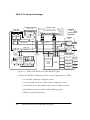
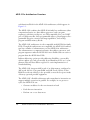
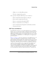
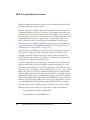
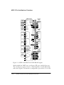
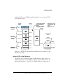
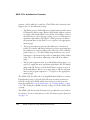
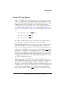
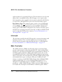
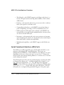
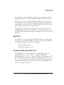
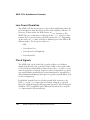
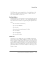
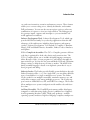
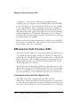
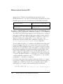
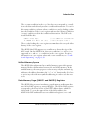
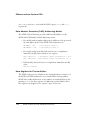
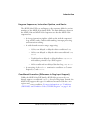
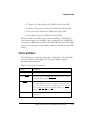
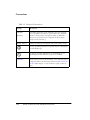
1 INTRODUCTION
Figure 1-0.
Table 1-0.
Listing 1-0.
Purpose
The ADSP-219x/2191 DSP Hardware Reference provides architectural
information on the ADSP-219x modified Harvard architecture Digital
Signal Processor (DSP) core and ADSP-2191 DSP product. The architectural descriptions cover functional blocks, buses, and ports, including all
the features and processes they support. For programming information,
see the ADSP-219x DSP Instruction Set Reference.
Audience
DSP system designers and programmers who are familiar with signal processing concepts are the primary audience for this manual. This manual
assumes that the audience has a working knowledge of microcomputer
technology and DSP-related mathematics.
DSP system designers and programmers who are unfamiliar with signal
processing can use this manual, but should supplement this manual with
other texts, describing DSP techniques.
All readers, particularly system designers, should refer to the DSP’s data
sheet for timing, electrical, and package specifications. For additional suggested reading, see “For more Information about Analog Products” on
page 1-31.
ADSP-219x/2191 DSP Hardware Reference
1-1
Overview—Why Fixed-Point DSP?
Overview—Why Fixed-Point DSP?
A digital signal processor’s data format determines its ability to handle signals of differing precision, dynamic range, and signal-to-noise ratios.
Because 16-bit, fixed-point DSP math is required for certain DSP coding
algorithms, using a 16-bit, fixed-point DSP can provide all the features
needed for certain algorithm and software development efforts. Also, a
narrower bus width (16-bit as opposed to 32- or 64-bit wide) leads to
reduced power consumption and other design savings. The extent to
which this is true depends on the fixed-point processor’s architecture.
High-level language programmability, large address spaces, and wide
dynamic range allow system development time to be spent on algorithms
and signal processing concerns, rather than assembly language coding,
code paging, and error handling. The ADSP-2191 DSP is a highly integrated, 16-bit fixed-point DSP that provides many of these design
advantages.
ADSP-219x Design Advantages
The ADSP-219x family DSPs are high-performance 16-bit DSPs for communications, instrumentation, industrial/control, voice/speech, medical,
military, and other applications. These DSPs provide a DSP core that is
compatible with previous ADSP-2100 family DSPs, but provides many
additional features. The ADSP-219x core combines with on-chip peripherals to form a complete system-on-a-chip. The off-core peripherals add
on-chip SRAM, integrated I/O peripherals, timer, and interrupt
controller.
The ADSP-219x architecture balances a high performance processor core
with high performance buses (PM, DM, DMA). In the core, every computational instruction can execute in a single cycle. The buses and
instruction cache provide rapid, unimpeded data flow to the core to maintain the execution rate.
1-2
ADSP-219x/2191 DSP Hardware Reference
Introduction
Figure 1-1 shows a detailed block diagram of the processor, illustrating the
following architectural features:
• Computation units—multiplier, ALU, shifter, and data register file
• Program sequencer with related instruction cache, interval timer,
and Data Address Generators (DAG1 and DAG2)
• Dual-blocked SRAM
• External ports for interfacing to off-chip memory, peripherals, and
hosts
• Input/Output (I/O) processor with integrated DMA controllers,
serial ports (SPORTs), serial peripheral interface (SPI) ports, and a
UART port
• JTAG Test Access Port for board test and emulation
Figure 1-1 also shows the three on-chip buses of the ADSP-219x: the Program Memory (PM) bus, Data Memory (DM) bus, and Direct Memory
Accessing (DMA) bus. The PM bus provides access to either instructions
or data. During a single cycle, these buses let the processor access two data
operands (one from PM and one from DM), and access an instruction
(from the cache).
The buses connect to the ADSP-219x’s external port, which provides the
processor’s interface to external memory, I/O memory-mapped, and boot
memory. The external port performs bus arbitration and supplies control
signals to shared, global memory and I/O devices.
ADSP-219x/2191 DSP Hardware Reference
1-3
ADSP-219x Design Advantages
AD D RESS
64× 24- B I T
DAG2
4×4×16
DA T A
AD D RESS
DA T A
JTAG
BLOCK1
TWO INDEPENDENT BLO CKS
CACHE
DAG1
BL OCK 0
ADSP-219x
DSP CORE
4×4×16
INTERN AL S RAM
INT ERRUPT CONT ROL LER/
TIM ER S/F L AG S
PROGRAM
SEQUENCER
6
TEST &
EM UL ATIO N
EXTERNAL
PORT
PM ADDRESS BUS
24
DM ADDRESS BUS
24
22
DMA
24 A D D R E S S
24
ADDR BUS
MUX
DMA
DATA
EXT ERNAL MEM ORY
INTERFACE
PM DATA BUS
24
DM DATA BUS
16
16
BUS
CONNECT
(PX)
DATA BUS
MUX
CORE
INT ERFACE
DATA
REGISTER
FILE
I/O PROCESSOR
24
INPUT
REG IST ERS
HOST PO RT
I/O R EG IST ER S
( M E MOR Y M A P PED )
RESUL T
REG IST ERS
MULT
16 × 16-BIT
BARREL
SHIF TER
ALU
CO NT ROL
ST AT US
BUF FERS
18
DMA
CONTROL LER
SERIAL PORTS
(3)
6
SPI P O RT S
(2)
2
UART PORT
(1)
Figure 1-1. ADSP-219x/ADSP-2191 DSP Block Diagram
Further, the ADSP-219x addresses the five central requirements for DSPs:
• Fast, flexible arithmetic computation units
• Unconstrained data flow to and from the computation units
• Extended precision and dynamic range in the computation units
• Dual address generators with circular buffering support
• Efficient program sequencing
1-4
ADSP-219x/2191 DSP Hardware Reference
Introduction
Unconstrained Data Flow. The ADSP-219x has a modified Harvard
architecture combined with a data register file. In every cycle, the DSP
can:
• Read two values from memory or write one value to memory
• Complete one computation
• Write up to three values back to the register file
Fast, Flexible Arithmetic. The ADSP-219x family DSPs execute all computational instructions in a single cycle. They provide both fast cycle
times and a complete set of arithmetic operations.
40-Bit Extended Precision. The DSP handles 16-bit integer and fractional
formats (two’s-complement and unsigned). The processors carry extended
precision through result registers in their computation units, limiting
intermediate data truncation errors.
Dual Address Generators. The DSP has two data address generators
(DAGs) that provide immediate or indirect (pre- and post-modify)
addressing. Modulus and bit-reverse operations are supported with memory page constraints on data buffer placement only.
Efficient Program Sequencing. In addition to zero-overhead loops, the
DSP supports quick setup and exit for loops. Loops are both nestable
(eight levels in hardware) and interruptable. The processors support both
delayed and non-delayed branches.
ADSP-219x Architecture Overview
An ADSP-219x is a single-chip microcomputer optimized for digital signal processing (DSP) and other high speed numeric processing
applications. These DSPs provide a complete system-on-a-chip, integrating a large, high-speed SRAM and I/O peripherals supported by a
dedicated DMA bus. The following sections summarize the features of
ADSP-219x/2191 DSP Hardware Reference
1-5
ADSP-219x Architecture Overview
each functional block in the ADSP-219x architecture, which appears in
Figure 1-1.
The ADSP-2191 combines the ADSP-219x family base architecture (three
computational units, two data address generators, and a program
sequencer) with three serial ports, two SPI-compatible ports, one UART
port, a DMA controller, three programmable timers, general-purpose Programmable Flag pins, extensive interrupt capabilities, and on-chip
program and data memory blocks.
The ADSP-2191 architecture is code compatible with ADSP-218x family
DSPs. Though the architectures are compatible, the ADSP-2191 architecture has a number of enhancements over the ADSP-218x architecture.
The enhancements to computational units, data address generators, and
program sequencer make the ADSP-2191 more flexible and even easier to
program than the ADSP-218x DSPs.
Indirect addressing options provide addressing flexibility—pre-modify
with no update, pre- and post-modify by an immediate 8-bit, two’s-complement value and base address registers for easier implementation of
circular buffering.
The ADSP-2191 integrates 64K words of on-chip memory configured as
32K words (24-bit) of program RAM, and 32K words (16-bit) of data
RAM. Power-down circuitry is also provided to meet the low power needs
of battery operated portable equipment.
The ADSP-2191’s flexible architecture and comprehensive instruction set
support multiple operations in parallel. For example, in one processor
cycle, the ADSP-2191 can:
• Generate an address for the next instruction fetch
• Fetch the next instruction
• Perform one or two data moves
1-6
ADSP-219x/2191 DSP Hardware Reference
Introduction
• Update one or two data address pointers
• Perform a computational operation
These operations take place while the processor continues to:
• Receive and transmit data through two serial ports
• Receive and/or transmit data from a host
• Receive or transmit data through the UART
• Receive or transmit data over two SPI ports
• Access external memory through the external memory interface
• Decrement the timers
DSP Core Architecture
The ADSP-219x instruction set provides flexible data moves and multifunction (one or two data moves with a computation) instructions. Every
single-word instruction can be executed in a single processor cycle. The
ADSP-219x assembly language uses an algebraic syntax for ease of coding
and readability. A comprehensive set of development tools supports program development.
Figure 1-1 on page 1-4 shows the architecture of the ADSP-219x core. It
contains three independent computational units: the ALU, the multiplier/accumulator, and the shifter. The computational units process 16-bit
data from the register file and have provisions to support multiprecision
computations. The ALU performs a standard set of arithmetic and logic
operations; division primitives also are supported. The multiplier performs single-cycle multiply, multiply/add, and multiply/subtract
operations. The multiplier has two 40-bit accumulators, which help with
overflow. The shifter performs logical and arithmetic shifts, normalization, denormalization, and derive exponent operations. The shifter can
ADSP-219x/2191 DSP Hardware Reference
1-7
ADSP-219x Architecture Overview
efficiently implement numeric format control, including multiword and
block floating-point representations.
Register-usage rules influence placement of input and results within the
computational units. For most operations, the computational units’ data
registers act as a data register file, permitting any input or result register to
provide input to any unit for a computation. For feedback operations, the
computational units let the output (result) of any unit be input to any
unit on the next cycle. For conditional or multifunction instructions,
there are restrictions limiting which data registers may provide inputs or
receive results from each computational unit. For more information, see
“Multifunction Computations” on page 2-58.
A powerful program sequencer controls the flow of instruction execution.
The sequencer supports conditional jumps, subroutine calls, and low
interrupt overhead. With internal loop counters and loop stacks, the
ADSP-2191 executes looped code with zero overhead; no explicit jump
instructions are required to maintain loops.
Two data address generators (DAGs) provide addresses for simultaneous
dual operand fetches (from data memory and program memory). Each
DAG maintains and updates four 16-bit address pointers. Whenever the
pointer is used to access data (indirect addressing), it is pre- or post-modified by the value of one of four possible modify registers. A length value
and base address may be associated with each pointer to implement automatic modulo addressing for circular buffers. Page registers in the DAGs
allow circular addressing within 64K word boundaries of each of the 256
memory pages, but these buffers may not cross page boundaries. Secondary registers duplicate all the primary registers in the DAGs; switching
between primary and secondary registers provides a fast context switch.
Efficient data transfer in the core is achieved by using internal buses:
• Program Memory Address (PMA) Bus
• Program Memory Data (PMD) Bus
1-8
ADSP-219x/2191 DSP Hardware Reference
Introduction
• Data Memory Address (DMA) Bus
• Data Memory Data (DMD) Bus
• DMA Address Bus
• DMA Data Bus
The internal address buses share a single external address bus, allowing
memory to be expanded off-chip, and the data buses share a single external
data bus. Boot memory space and external I/O memory space also share
the external buses.
Program memory can store both instructions and data, permitting the
ADSP-219x to fetch two operands in a single cycle, one from program
memory and one from data memory. The DSP’s dual memory buses also
let the ADSP-219x core fetch an operand from data memory and the next
instruction from program memory in a single cycle.
DSP Peripherals Architecture
Figure 1-1 on page 1-4 shows the DSP’s on-chip peripherals, which
include the external memory interface, host port, serial ports, SPI compatible ports, UART port, JTAG test and emulation port, timers, flags, and
interrupt controller. Figure 1-2 illustrates a typical ADSP-2191 system
with peripheral connections.
The ADSP-2191 has a 16-bit host port with DMA capability that provides external hosts access to on-chip memory. This parallel port consists
of a multiplexed data/address bus and provides a low-service overhead data
move capability. Configurable for 8- or 16-bit data bus widths, this port
provides a glueless interface to a wide variety of 8- and 16-bit microcontrollers. Two chip-selects provide hosts access to the DSP’s entire memory
map. The DSP is bootable through this port.
The ADSP-2191 also has an external memory interface that is shared by
the DSP’s core, the DMA controller, and DMA capable peripherals,
ADSP-219x/2191 DSP Hardware Reference
1-9
ADSP-219x Architecture Overview
ADSP-2191M
XTA L
ADDR21–0
ADDR21–0
DATA15–8
DATA15–8
TMR2–0
BOOT
AND OP
MODE
MS3–0
CS
RD
OE
DF /PF 7
WR
WE
BYPA SS
ACK
ACK
CONT ROL
BMODE1–0
OPM OD E
DATA15–8
DATA7–0
TF S0
BMS
DT0
( O PT IO N A L )
OE
RFS0
WE
ACK
SPOR T 1
BR
TCLK1
BG
BGH
TF S1
( O PT IO N A L )
EXTERNAL
I/O M EM O RY
( O P T IO N A L )
DT1
ADDR21–0
RCLK1
DATA15–8
DATA7–0
RFS1
DR1
SER IA L
DEVICE
CS
RCLK0
DR0
SER IA L
DEVICE
B O OT
MEMOR Y
( O PT IO N A L )
ADDR21–0
SPOR T 0
TCLK0
SER IA L
DEVICE
DATA7–0
DATA7–0
MSEL6–0/PF6–0
CLOCK
M UL T IPLY
AND
RANGE
( O PT IO N A L )
CLKOUT
DA T A
TIM ER
OU T OR
CAPTURE
EXT ER NA L
MEMOR Y
CLKIN
AD DRESS
CLOCK
OR
CRYSTAL
IO M S
CS
SPOR T 2
OE
TCLK2/SCK0
WE
TF S2 /M OSI0 SPI0
ACK
DT 2 /M ISO0
HOST
PR OC ESSOR
RCLK2/SCK1
( O PT IO N A L )
( O P T IO N A L )
RF S2/M OSI1 SPI1
DR2 /MISO1
HAD15–0
HA16
UART
UART
DEVICE
( O PT IO N A L )
HCMS
ADDR15–0/
DATA15–0
ADDR16
CS0
RXD
HC IO MS
TXD
HRD
RD
RESET
6
JTAG
CS1
HWR
WR
HACK
ACK
HALE
AL E
HACK_P
Figure 1-2. ADSP-219x/ADSP-2191 DSP Block Diagram
which include the UART port, serial ports, SPI ports, and the host port.
The external port consists of an 8- or 16-bit data bus, a 22-bit address bus,
and control signals. The data bus is configurable to provide an 8- or 16-bit
1-10
ADSP-219x/2191 DSP Hardware Reference
Introduction
interface to external memory. Support for word packing lets the DSP
access 16- or 24-bit words from external memory regardless of the external
data bus width. When configured for an 8-bit interface, the unused eight
lines provide eight programmable, bidirectional general purpose Programmable Flag lines, six of which can be mapped to software condition
signals.
The memory DMA controller lets the ADSP-2191 transfer data to and
from internal and external memory. On-chip peripherals also can use this
port for DMA transfers to and from memory.
The ADSP-2191 can respond to up to 16 interrupt sources at any given
time: three internal (stack, emulator kernel, and power-down), two external (emulator and reset), and twelve user-defined (peripherals) interrupt
requests. Programmers assign a peripheral to one of the 12 user defined
interrupt requests. These assignments determine the priority of each
peripheral for interrupt service. Several peripherals can be combined on a
single interrupt request line.
There are three serial ports on the ADSP-2191 that provide a complete
synchronous, full-duplex serial interface. This interface includes optional
companding in hardware and a wide variety of framed or frameless data
transmit and receive modes of operation. Each serial port can transmit or
receive an internal or external, programmable serial clock and frame syncs.
Each serial port supports 128-channel Time Division Multiplexing.
The ADSP-2191 provides up to sixteen general-purpose I/O pins, which
are programmable as either inputs or outputs. Eight of these pins are dedicated general purpose Programmable Flag pins. The other eight are
multifunctional pins, acting as general purpose I/O pins when the DSP
connects to an 8-bit external data bus and acting as the upper eight data
pins when the DSP connects to a 16-bit external data bus. These Programmable Flag pins can implement edge- or level-sensitive interrupts. The
execution of conditional instructions can be based on some of the Programmable Flag pins.
ADSP-219x/2191 DSP Hardware Reference
1-11
ADSP-219x Architecture Overview
Three programmable interval timers generate periodic interrupts. Each
timer can be independently set to operate in one of three modes:
• Pulse Waveform Generation mode
• Pulse Width Count/Capture mode
• External Event Watchdog mode
Each timer has one bi-directional pin and four registers that implement its
mode of operation: a configuration register, a count register, a period register, and a pulsewidth register. A single status register supports all three
timers. A bit in the mode status register globally enables or disables all
three timers, and a bit in each timer’s configuration register enables or disables the corresponding timer independently of the others.
Memory Architecture
The ADSP-2191 provides 64K words of on-chip memory. This memory is
divided into two 32K blocks located on memory Page 0 in the DSP’s
memory map. In addition to the internal and external memory space, the
ADSP-2191 can address two additional and separate memory spaces: I/O
space and boot space.
As shown in Figure 1-3, the DSP’s two internal memory blocks populate
all of Page 0. The entire DSP memory map consists of 256 pages (pages
0−255), and each page is 64K words long. External memory space consists
of four memory banks (banks 3–0) and supports a wide variety of SRAM
memory devices. Each bank is selectable using the memory select pins
(MS3-0) and has configurable page boundaries, waitstates, and waitstate
modes. The 1K word of on-chip boot-ROM populates the lower 1K
addresses of page 255. Other than page 0 and page 255, the remaining
254 pages are addressable off-chip. I/O memory pages differ from external
memory pages in that I/O pages are 1K word long, and the external I/O
pages have their own select pin (IOMS). Pages 0–7 of I/O memory space
reside on-chip and contain the configuration registers for the peripherals.
1-12
ADSP-219x/2191 DSP Hardware Reference
Introduction
Both the DSP core and DMA-capable peripherals can access the DSP’s
entire memory map.
64K WORD
MEMORY
PAGES
ADDRESS
0xFF FFFF
RESERVED
INTERNAL
MEMORY
PAGE 255
BOOT ROM, 24-BIT
0xFF 0400
LOWER PAGE BOUNDARIES
ARE CONFIGURABLE FOR
BANKS OF EXTERNAL
MEMORY.
BOUNDARIES SHOWN ARE
BANK SIZES AT RESET.
MEMORY SELECTS (MS)
FOR PORTIONS OF
THE MEMORY MAP
APPEAR
WITH THE SELECTED
MEMORY.
ADDRESS
0xFF 0000
0xFE FFFF
PAGES 192–254
BANK3
(MS3)
0xC0 0000
I/O MEMORY
PAGES 128–191
0x80 0000
EXTERNAL
MEMORY
PAGES 64–127
(16- BIT)
16- BIT
BANK2
(MS2)
64K WORD
PAGES 1–254
1K WORD
PAGES 0–7
BANK0
(MS0)
BLOCK1, 16-BIT
PAGE 0
BLOCK0, 24-BIT
ADDRESS
0xFF : 0x3FF
0x01 0000
INTERNAL
MEMORY
1K WORD
PAGES 8–255
16- BIT
(BMS)
BANK1
(MS1)
0x40 0000
PAGES 1–63
BOOT
MEMORY
0x00 8000
0x00 0000
0x01 0000
EXTERNAL
(IOMS)
INTERNAL
0x08 : 0x000
0x00 : 0x000
Figure 1-3. ADSP-2191 Internal/External Memory, Boot Memory, and
I/O Memory Maps
Internal (On-chip) Memory
The ADSP-2191’s unified program and data memory space consists of
16M locations that are accessible through two 24-bit address buses, the
PMA and DMA buses. The DSP uses slightly different mechanisms to
ADSP-219x/2191 DSP Hardware Reference
1-13
ADSP-219x Architecture Overview
generate a 24-bit address for each bus. The DSP has three functions that
support access to the full memory map.
• The DAGs generate 24-bit addresses for data fetches from the entire
DSP memory address range. Because DAG index (address) registers
are 16 bits wide and hold the lower 16-bits of the address, each of
the DAGs has its own 8-bit page register (DMPGx) to hold the most
significant eight address bits. Before a DAG generates an address,
the program must set the DAG’s DMPGx register to the appropriate
memory page.
• The program sequencer generates the addresses for instruction
fetches. For relative addressing instructions, the program sequencer
bases addresses for relative jumps, calls, and loops on the 24-bit Program Counter (PC). For direct addressing instructions (two-word
instructions), the instruction provides an immediate 24-bit address
value. The PC allows linear addressing of the full 24 bit address
range.
• The program sequencer relies on an 8-bit Indirect Jump page (IJPG)
register to supply the most significant eight address bits for indirect
jumps and calls that use a 16-bit DAG address register for part of
the branch address. Before a cross page jump or call, the program
must set the program sequencer’s IJPG register to the appropriate
memory page.
The ADSP-2191 has 1K word of on-chip ROM that holds boot routines.
If peripheral booting is selected, the DSP starts executing instructions
from the on-chip boot ROM, which starts the boot process from the
selected peripheral. For more information, see “Booting Modes” on page
1-21. The on-chip boot ROM is located on Page 255 in the DSP’s memory map.
The ADSP-2191 has internal I/O memory for peripheral control and status registers. For more information, see the I/O memory space discussion
on page 1-15.
1-14
ADSP-219x/2191 DSP Hardware Reference
Introduction
External (Off-chip) Memory
Each of the ADSP-2191’s off-chip memory spaces has a separate control
register, so applications can configure unique access parameters for each
space. The access parameters include read and write wait counts, waitstate
completion mode, I/O clock divide ratio, write hold time extension,
strobe polarity, and data bus width. The core clock and peripheral clock
ratios influence the external memory access strobe widths. For more information, see “Clock Signals” on page 1-20. The off-chip memory spaces
are:
• External memory space (MS3-0 pins)
• I/O memory space (IOMS pin)
• Boot memory space (BMS pin)
All of these off-chip memory spaces are accessible through the external
port, which can be configured for 8-bit or 16-bit data widths.
External Memory Space. External memory space consists of four memory
banks. These banks can contain a configurable number of 64K word
pages. At reset, the page boundaries for external memory have Bank 0 containing pages 1−63, Bank 1 containing pages 64−127, Bank 2 containing
pages 128−191, and Bank 3 containing pages 192−254. The MS3-0 memory bank pins select Bank 3-0, respectively. The external memory interface
decodes the eight MSBs of the DSP program address to select one of the
four banks. Both the DSP core and DMA-capable peripherals can access
the DSP’s external memory space.
I/O Memory Space. The ADSP-2191 supports an additional external
memory called I/O memory space. This space is designed to support simple connections to peripherals (such as data converters and external
registers) or to bus interface ASIC data registers. I/O space supports a total
of 256K locations. The first 8K addresses are reserved for on-chip peripherals. The upper 248K addresses are available for external peripheral
devices and are selected with the IOMS pin. The DSP’s instruction set pro-
ADSP-219x/2191 DSP Hardware Reference
1-15
ADSP-219x Architecture Overview
vides instructions for accessing I/O space. These instructions use an 18-bit
address that is assembled from an 8-bit I/O page (IOPG) register and a
10-bit immediate value supplied in the instruction. Both the ADSP-219x
core and a host (through the host port) can access I/O memory space.
Boot Memory Space. Boot memory space consists of one off-chip bank
with 253 pages. The BMS pin selects boot memory space. Both the DSP
core and DMA-capable peripherals can access the DSP’s off-chip boot
memory space. If the DSP is configured to boot from boot memory space,
the DSP starts executing instructions from the on-chip boot ROM, which
starts booting the DSP from boot memory. For more information, see
“Booting Modes” on page 1-21.
Interrupts
The interrupt controller lets the DSP respond to seventeen interrupts with
minimum overhead. The controller implements an interrupt priority
scheme that lets programs assign interrupt priorities to each peripheral.
For more information, see “ADSP-2191 Interrupts” on page C-1.
DMA Controller
The ADSP-2191 has a DMA controller that supports automated data
transfers with minimal overhead for the DSP core. Cycle stealing DMA
transfers can occur between the ADSP-2191’s internal memory and any of
its DMA capable peripherals. Additionally, DMA transfers also can be
accomplished between any of the DMA capable peripherals and external
devices connected to the external memory interface. DMA capable peripherals include the host port, serial ports, SPI ports, UART port, and
memory-to-memory (memDMA) DMA channel. Each individual DMA
capable peripheral has one or more dedicated DMA channels. For a
description of each DMA sequence, the DMA controller uses a set of
parameters—called a DMA descriptor. When successive DMA sequences
are needed, these descriptors can be linked or chained together. When
1-16
ADSP-219x/2191 DSP Hardware Reference
Introduction
chained, the completion of one DMA sequence auto-initiates and starts
the next sequence. DMA sequences do not contend for bus access with the
DSP core, instead DMAs “steal” cycles to access memory.
Host Port
The ADSP-2191’s host port functions as a slave on the external bus of an
external host. The host port interface lets a host read from or write to the
DSP’s memory space, boot space, or internal I/O space. Examples of hosts
include external microcontrollers, microprocessors, or ASICs.
The host port is a multiplexed address and data bus that provides an 8- or
16-bit data path and operates using an asynchronous transmission protocol. To access the DSP’s internal memory space, a host steals one cycle per
access from the DSP. A host access to the DSP’s external memory uses the
external port interface and does not stall (or steal cycles from) the DSP’s
core. Because a host can access internal I/O memory space, a host can control any of the DSP’s I/O mapped peripherals.
DSP Serial Ports (SPORTs)
The ADSP-2191 incorporates three complete synchronous serial ports
(SPORT0, SPORT1, and SPORT2) for serial and multiprocessor communications. The SPORTs support the following features:
• Bidirectional operation—each SPORT has independent transmit
and receive pins.
• Buffered (eight-deep) transmit and receive ports—each port has a
data register for transferring data words to and from other DSP
components and shift registers for shifting data in and out of the
data registers.
• Clocking—each transmit and receive port either can use an external
serial clock (≤75 MHz) or generate its own, in frequencies ranging
from 1144 Hz to 75 MHz.
ADSP-219x/2191 DSP Hardware Reference
1-17
ADSP-219x Architecture Overview
• Word length—each SPORT supports serial data words from 3- to
16-bits in length transferred in big endian (MSB) or little endian
(LSB) format.
• Framing—each transmit and receive port can run with or without
frame sync signals for each data word.
• Companding in hardware—each SPORT can perform A-law or
µ-law companding, according to ITU recommendation G.711.
• DMA operations with single-cycle overhead—each SPORT can
automatically receive and transmit multiple buffers of memory data,
one data word each DSP cycle.
• Interrupts—each transmit and receive port generates an interrupt
upon completing the transfer of a data word or after transferring an
entire data buffer or buffers through DMA.
• Multichannel capability—each SPORT supports the H.100 standard.
Serial Peripheral Interface (SPI) Ports
The DSP has two SPI-compatible ports, which enable the DSP to communicate with multiple SPI compatible devices. These ports are
multiplexed with SPORT2, so either SPORT2 or the SPI ports are active
depending on the state of the OPMODE pin or OPMODE bit. To change the
mode, the pin can be changed during hardware or software reset, or the bit
can be changed at runtime.
The SPI interface uses three pins for transferring data: two data pins (Master Output-Slave Input, MOSIx, and Master Input-Slave Output, MISOx)
and a clock pin (Serial Clock, SCKx). Two SPI chip select input pins
(SPISSx) let other SPI devices select the DSP, and fourteen SPI chip select
output pins (SPIxSEL7-1) let the DSP select other SPI devices. The SPI
select pins are re-configured Programmable Flag pins. Using these pins,
1-18
ADSP-219x/2191 DSP Hardware Reference
Introduction
the SPI ports provide a full duplex, synchronous serial interface, which
supports both master and slave modes and multiple master environments.
Each SPI port’s baud rate and clock phase/polarities are programmable,
and each has an integrated DMA controller, configurable to support both
transmit and receive data streams. The SPI’s DMA controller can only service uni-directional accesses at any given time.
During transfers, the SPI ports simultaneously transmit and receive by
serially shifting data in and out on their two serial data lines. The serial
clock line synchronizes the shifting and sampling of data on the two serial
data lines.
UART Port
The UART port provides a simplified UART interface to another peripheral or host. It performs full duplex, asynchronous transfers of serial data.
The UART port supports two modes of operation:
• PIO (programmed I/O)
• DMA (direct memory access)
Programmable Flag (PFx) Pins
The ADSP-2191 has sixteen bi-directional, general-purpose I/O, Programmable Flag (PF15-0) pins. The PF7-0 pins are dedicated to
general-purpose I/O. The PF15-8 pins serve either as general-purpose I/O
pins (if the DSP is connected to an 8-bit external data bus) or serve as
DATA15-8 lines (if the DSP is connected to a 16-bit external data bus). The
Programmable Flag pins have special functions for clock multiplier selection and for SPI port operation.
ADSP-219x/2191 DSP Hardware Reference
1-19
ADSP-219x Architecture Overview
Low-Power Operation
The ADSP-2191 has four low-power options that significantly reduce the
power dissipation when the device operates under standby conditions. To
enter any of these modes, the DSP executes an IDLE instruction. The
ADSP-2191 uses configuration of the bits in the PLLCTL register to select
between the low-power modes as the DSP executes the Idle. Depending
on the mode, an Idle shuts off clocks to different parts of the DSP in the
different modes. The low-power modes are:
• Idle
• Powerdown Core
• Powerdown Core/Peripherals
• Powerdown All
Clock Signals
The ADSP-2191 can be clocked by a crystal oscillator or a buffered,
shaped clock derived from an external clock oscillator. If a crystal oscillator is used, the crystal should be connected across the CLKIN and XTAL pins,
with two capacitors connected. Capacitor values are dependent on crystal
type and should be specified by the crystal manufacturer. A parallel-resonant, fundamental frequency, microprocessor-grade crystal should be used
for this configuration.
If a buffered, shaped clock is used, this external clock connects to the
DSP’s CLKIN pin. CLKIN input cannot be halted, changed, or operated
below the specified frequency during normal operation. This clock signal
should be a TTL-compatible signal. When an external clock is used, the
XTAL input must be left unconnected.
1-20
ADSP-219x/2191 DSP Hardware Reference
Introduction
The DSP provides a user programmable 1x to 31x multiplication of the
input clock—including some fractional values—to support 128 external-to-internal (DSP core) clock ratios.
Booting Modes
The ADSP-2191 has seven mechanisms for automatically loading internal
program memory after reset. The BMODE2-0 pins, sampled during hardware
reset, and three bits in the Reset Configuration Register implement these
modes:
• Boot from 16-bit external memory
• Boot from 8-bit EPROM
• Boot from host
• Execute from 8-bit external memory (No Boot)
• Boot from UART
• Boot from SPI 4 kbits
• Boot from SPI 512 kbits
JTAG Port
The JTAG port on the ADSP-2191 supports the IEEE standard 1149.1
Joint Test Action Group (JTAG) standard for system test. This standard
defines a method for serially scanning the I/O status of each component in
a system. Emulators use the JTAG port to monitor and control the DSP
during emulation. Emulators using this port provide full-speed emulation
with access to inspect and modify memory, registers, and processor stacks.
JTAG-based emulation is non-intrusive and does not affect target system
loading or timing.
ADSP-219x/2191 DSP Hardware Reference
1-21
Development Tools
Development Tools
The ADSP-219x is supported by VisualDSP®, an easy-to-use project
management environment, comprised of an Integrated Development
Environment (IDE) and Debugger. VisualDSP lets you manage projects
from start to finish from within a single, integrated interface. Because the
project development and debug environments are integrated, you can
move easily between editing, building, and debugging activities.
Flexible Project Management. The IDE provides flexible project management for the development of DSP applications. The IDE includes access
to all the activities necessary to create and debug DSP projects. You can
create or modify source files or view listing or map files with the IDE Editor. This powerful Editor is part of the IDE and includes multiple
language syntax highlighting, OLE drag and drop, bookmarks, and standard editing operations such as undo/redo, find/replace, copy/paste/cut,
and go to.
Also, the IDE includes access to the DSP C Compiler, C Runtime
Library, Assembler, Linker, Loader, Simulator, and Splitter. You specify
options for these Tools through Property Page dialogs. Property Page dialogs are easy to use and make configuring, changing, and managing your
projects simple. These options control how the tools process inputs and
generate outputs, and the options have a one-to-one correspondence to
the tools’ command line switches. You can define these options once or
modify them to meet changing development needs. You also can access
the Tools from the operating system command line if you choose.
Greatly Reduced Debugging Time. The Debugger has an easy-to-use,
common interface for all processor simulators and emulators available
through Analog Devices and third parties or custom developments. The
Debugger has many features that greatly reduce debugging time. You can
view C source interspersed with the resulting Assembly code. You can profile execution of a range of instructions in a program; set simulated
watchpoints on hardware and software registers, program and data mem-
1-22
ADSP-219x/2191 DSP Hardware Reference
Introduction
ory; and trace instruction execution and memory accesses. These features
enable you to correct coding errors, identify bottlenecks, and examine
DSP performance. You can use the custom register option to select any
combination of registers to view in a single window. The Debugger can
also generate inputs, outputs, and interrupts so you can simulate real
world application conditions.
Software Development Tools. Software Development Tools, which support the ADSP-219x family, let you develop applications that take full
advantage of the architecture, including shared memory and memory
overlays. Software Development Tools include C Compiler, C Runtime
Library, DSP and Math Libraries, Assembler, Linker, Loader, Simulator,
and Splitter.
C/C++ Compiler & Assembler. The C/C++ Compiler generates efficient
code that is optimized for both code density and execution time. The
C/C++ Compiler allows you to include Assembly language statements
inline. Because of this, you can program in C and still use Assembly for
time-critical loops. You can also use pretested Math, DSP, and C Runtime
Library routines to help shorten your time to market. The ADSP-219x
family assembly language is based on an algebraic syntax that is easy to
learn, program, and debug.
Linker & Loader. The Linker provides flexible system definition through
Linker Description Files (.LDF). In a single LDF, you can define different
types of executables for a single or multiprocessor system. The Linker
resolves symbols over multiple executables, maximizes memory use, and
easily shares common code among multiple processors. The Loader supports creation of PROM, host, SPI, and UART boot images. The Loader
allows multiprocessor system configuration with smaller code and faster
boot time.
3rd-Party Extensible. The VisualDSP environment enables third-party
companies to add value using Analog Devices’ published set of Application Programming Interfaces (API). Third party products—realtime
operating systems, emulators, high-level language compilers, multiproces-
ADSP-219x/2191 DSP Hardware Reference
1-23
Differences from Previous DSPs
sor hardware —can interface seamlessly with VisualDSP thereby
simplifying the tools integration task. VisualDSP follows the COM API
format. Two API tools, Target Wizard and API Tester, are also available
for use with the API set. These tools help speed the time-to-market for
vendor products. Target Wizard builds the programming shell based on
API features the vendor requires. The API tester exercises the individual
features independently of VisualDSP. Third parties can use a subset of
these APIs that meet their application needs. The interfaces are fully supported and backward compatible.
Further details and ordering information are available in the VisualDSP
Development Tools data sheet. This data sheet can be requested from any
Analog Devices sales office or distributor.
Differences from Previous DSPs
This section identifies differences between the ADSP-219x DSPs and previous ADSP-2100 family DSPs: ADSP-210x, ADSP-211x, ADSP-217x,
and ADSP-218x. The ADSP-219x preserves much of the core ADSP-2100
family architecture, while extending performance and functionality. For
background information on previous ADSP-2100 family DSPs, see the
ADSP-2100 Family User’s Manual.
The following sections describe key differences and enhancements of the
ADSP-219x over previous ADSP-2100 family DSPs. These enhancements
also lead to some differences in the instruction sets between these DSPs.
For more information, see the ADSP-219x DSP Instruction Set Reference.
Computational Units and Data Register File
The ADSP-219x DSP’s computational units differ from the
ADSP-218x’s, because the ADSP-219x data registers act as a register file
for unconditional, single-function instructions. In these instructions, any
data register may be an input to any computational unit. For conditional
1-24
ADSP-219x/2191 DSP Hardware Reference
Introduction
and/or multifunction instructions, the ADSP-219x and ADSP-218x DSP
families have the same data register usage restrictions — AX and AY for
ALU, MX and MY for the multiplier, and SI for shifter inputs. For more
information, see “Computational Units” on page 2-1.
Arithmetic Status (ASTAT) Register Latency
The ADSP-219x ASTAT register has a one cycle effect latency. This issue is
discussed on page 2-18.
Norm and Exp Instruction Execution
The ADSP-219x Norm and Exp instructions execute slightly differently
from previous ADSP-218x DSPs. This issue is discussed on page 2-45.
Shifter Result (SR) Register as Multiplier Dual Accumulator
The ADSP-219x architecture introduces a new 16-bit register in addition
to the SR0 and SR1 registers, the combination of which comprise the 40-bit
wide SR register on the ADSP-218x DSPs. This new register, called SR2,
can be used in multiplier or shift operations (lower 8 bits) and as a full
16-bit-wide scratch register. As a result, the ADSP-219x DSP has two
40-bit-wide accumulators, MR and SR. The SR dual accumulator has
replaced the multiplier feedback register MF, as shown in the following
example:
ADSP-218x Instruction
ADSP-219x Instruction (Replacement)
MF=MR+MX0*MY1(UU);
SR=MR+MX0*MY1(UU);
IF NOT MV MR=AR*MF;
IF NOT MV MR=AR*SR2;
Shifter Exponent (SE) Register is not Memory Accessible
The ADSP-218x DSPs use SE as a data or scratch register. The SE register
of the ADSP-219x architecture is not accessible from the data or program
ADSP-219x/2191 DSP Hardware Reference
1-25
Differences from Previous DSPs
memory buses. Therefore, the multifunction instructions of the
ADSP-218x that use SE as a data or scratch register, should use one of the
data file registers (DREG) as a scratch register on the ADSP-219x DSP.
ADSP-218x Instruction
ADSP-219x Instruction (Replacement)
SR=Lshift MR1(HI),
SE=DM(I6,M5);
SR=Lshift MR1(HI),
AX0=DM(I6,M5);
Conditions (SWCOND) and Condition Code (CCODE) Register
The ADSP-219x DSP changes support for the ALU Signed (AS) condition
and supports additional arithmetic and status condition testing with the
Condition Code (CCODE) register and Software Condition (SWCOND) test.
The two conditions are SWCOND and Not SWCOND. The usage of the
ADSP-219x’s and most ADSP-218x’s arithmetic conditions (EQ, NE, GE,
GT, LE, LT, AV, Not AV, AC, Not AC, MV, Not MV) are compatible.
The new Shifter Overflow (SV) condition of the ADSP-219x architecture
is a good example of how the CCODE register and SWCOND test work. The
ADSP-219x DSP’s Arithmetic Status (ASTAT) register contains a bit indicating the status of the shifter’s result. The shifter is a computational unit
that performs arithmetic or logical bitwise shifts on fields within a data
register. The result of the operation goes into the Shifter Result ( SR2, SR1,
and SR0, which are combined into SR) register. If the result overflows the
SR register, the Shifter Overflow ( SV) bit in the ASTAT register records this
overflow/underflow condition for the SR result register (0 = No overflow
or underflow, 1 = Overflow or underflow).
For the most part, bits (status condition indicators) in the ASTAT register
correspond to condition codes that appear in conditional instructions. For
example, the AZ (ALU Zero) bit in ASTAT corresponds to the EQ (ALU
result equals zero) condition and would be used in code like this:
IF EQ AR = AX0 + AY0;
/* if the ALU result (AR) register is zero, add AX0 and AY0 */
1-26
ADSP-219x/2191 DSP Hardware Reference
Introduction
The SV status condition in the ASTAT bits does not correspond to a condition code that can be directly used in a conditional instruction. To test for
this status condition, software selects a condition to test by loading a value
into the Condition Code (CCODE) register and uses the Software Condition
(SWCOND) condition code in the conditional instruction. The DSP code
would look like this:
CCODE = 0x09; Nop;
IF SWCOND SR = MR0 * SR1 (UU);
// set CCODE for SV condition
// mult unsigned X and Y
The Nop after loading the CCODE register accommodates the one cycle effect
latency of the CCODE register.
The ADSP-218x DSP supports two conditions to detect the sign of the
ALU result. On the ADSP-219x, these two conditions (Pos and Neg) are
supported as AS and Not AS conditions in the CCODE register. For more
information on CCODE register values and SWCOND conditions, see “Conditional Sequencing” on page 3-39.
Unified Memory Space
The ADSP-219x architecture has a unified memory space with separate
memory blocks to differentiate between 24- and 16-bit memory. In the
unified memory, the term program or data memory only has semantic significance; the address determines the “PM” or “DM” functionality. It is best
to revise any code with non-symbolic addressing in order to use the new
tools.
Data Memory Page (DMPG1 and DMPG2) Registers
The ADSP-219x processor introduces a paged memory architecture that
uses 16-bit DAG registers to access 64K pages. The 16-bit DAG registers
correspond to the lower 16 bits of the DSP’s address buses, which are
24-bit wide. To store the upper 8 bits of the 24-bit address, the
ADSP-219x DSP architecture uses two additional registers, DMPG1 and
ADSP-219x/2191 DSP Hardware Reference
1-27
Differences from Previous DSPs
DMPG2. DMPG1
and DMPG2 work with the DAG registers I0-I3 and I4-I7,
respectively.
Data Address Generator (DAG) Addressing Modes
The ADSP-219x architecture provides additional flexibility over the
ADSP-218x DSP family in DAG addressing modes:
• Pre-modify without update addressing in addition to the post-modify with update mode of the ADSP-218x instruction set:
DM(IO+M1) = AR;
/* pre-modify syntax */
DM(IO+=M1) = AR;
/* post-modify syntax */
• Pre-modify and post-modify with an 8-bit two’s-complement
immediate modify value instead of an M register:
AX0 = PM(I5+-4);
/* pre-modify syntax (for modifier = -4)*/
AX0 = PM(I5+=4); /* post-modify syntax (for modifier = 4) */
• DAG modify with an 8-bit two’s-complement immediate-modify
value:
Modify(I7+=0x24);
Base Registers for Circular Buffers
The ADSP-219x processor eliminates the existing hardware restriction of
the ADSP-218x DSP architecture on a circular buffer starting address.
ADSP-219x enables declaration of any number of circular buffers by designating B0-B7 as the base registers for addressing circular buffers; these
base registers are mapped to the “register” space on the core.
1-28
ADSP-219x/2191 DSP Hardware Reference
Introduction
Program Sequencer, Instruction Pipeline, and Stacks
The ADSP-219x DSP core and inputs to the sequencer differ for various
members of the ADSP-219x family DSPs. The main differences between
the ADSP-218x and ADSP-219x sequencers are that the ADSP-219x
sequencer has:
• A 6-stage instruction pipeline, which works with the sequencer’s
loop and PC stacks, conditional branching, interrupt processing,
and instruction caching.
• A wider branch execution range, supporting:
• 13-bit, non-delayed or delayed relative conditional Jump
• 16-bit, non-delayed or delayed relative unconditional Jump
or Call
• Conditional non-delayed or delayed indirect Jump or Call
with address pointed to by a DAG register
• 24-bit conditional non-delayed absolute long Jump or Call
• A narrowing of the Do/Until termination conditions to Counter
Expired (CE) and Forever.
Conditional Execution (Difference in Flag Input Support)
Unlike the ADSP-218x DSP family, ADSP-219x processors do not
directly support a conditional Jump/Call based on flag input. Instead, the
ADSP-219x supports this type of conditional execution with the CCODE
register and SWCOND condition. For more information, see “Conditions
(SWCOND) and Condition Code (CCODE) Register” on page 1-26.
ADSP-219x/2191 DSP Hardware Reference
1-29
Differences from Previous DSPs
The ADSP-219x architecture has 16 programmable flag pins that can be
configured as either inputs or outputs. The flags can be checked either by
reading the FLAGS register, or by using a software condition flag.
ADSP-218x Instruction
ADSP-219x Instruction (Replacement)
If Not FLAG_IN AR=MR0 And 8192; SWCOND=0x03;
If Not SWCOND AR=MR0 And 8192;
IOPG = 0x06;
AX0=IO(FLAGS);
AXO=Tstbit 11 OF AXO;
If EQ AR=MRO And 8192;
Execution Latencies (Different for JUMP Instructions)
The ADSP-219x processor has an instruction pipeline (unlike ADSP-218x
DSPs) and branches execution for immediate Jump and Call instructions
in four clock cycles if the branch is taken. To minimize branch latency,
ADSP-219x programs can use the delayed branch option on jumps and
calls, reducing branch latency by two cycles. This savings comes from execution of two instructions following the branch before the Jump/Call
occurs.
Instruction Set Enhancements
ADSP-219x provides near source code compatibility with the previous
family members, easing the process of porting code. All computational
instructions (but not all registers) from previous ADSP-2100 family DSPs
1-30
ADSP-219x/2191 DSP Hardware Reference
Introduction
are available in ADSP-219x. New instructions, control registers, or other
facilities, required to support the new feature set of ADSP-219x core are:
• Program flow control differences (pipeline execution and changes to
looping)
• Memory accessing differences (DAG support and memory map)
• Peripheral I/O differences (additional ports and added DMA functionality)
For more information, see the ADSP-219x DSP Instruction Set Reference.
For more Information about Analog
Products
Analog Devices is online on the internet at http://www.analog.com. Our
Web pages provide information on the company and products, including
access to technical information and documentation, product overviews,
and product announcements.
You may also obtain additional information about Analog Devices and its
products in any of the following ways:
• Visit our World Wide Web site at www.analog.com
• FAX questions or requests for information to 1(781)461-3010.
• Access the DSP Division File Transfer Protocol (FTP) site at ftp
ftp.analog.com or ftp 137.71.23.21 or ftp://ftp.analog.com.
ADSP-219x/2191 DSP Hardware Reference
1-31
For Technical or Customer Support
For Technical or Customer Support
You can reach our Customer Support group in the following ways:
• E-mail questions to [email protected] or
[email protected] (European customer support)
• Telex questions to 924491, TWX:710/394-6577
• Cable questions to ANALOG NORWOODMASS
• Contact your local ADI sales office or an authorized ADI distributor
• Send questions by mail to:
Analog Devices, Inc.
DSP Division
One Technology Way
P.O. Box 9106
Norwood, MA 02062-9106
USA
What’s New in this Manual
This is the first edition of the ADSP-219x DSP Hardware Reference. Summaries of changes between editions will start with the next edition.
Related Documents
For more information about Analog Devices DSPs and development
products, see the following documents:
• ADSP-2191 DSP Microcomputer Data Sheet
• ADSP-219x DSP Instruction Set Reference
• VisualDSP++ User’s Guide for ADSP-21xx Family DSPs
1-32
ADSP-219x/2191 DSP Hardware Reference
Introduction
• C Compiler and Library Manual for ADSP-219x Family DSPs
• Assembler and Preprocessor Manual for ADSP-219x Family DSPs
• Linker and Utilities Manual for ADSP-219x Family DSPs
• Getting Started Guide for ADSP-219x Family DSPs
All the manuals are included in the software distribution CD-ROM. To
access these manuals, use the Help Topics command in the VisualDSP++
environment’s Help menu and select the Online Manuals. From this Help
topic, you can open any of the manuals, which are in Adobe Acrobat PDF
format.
Conventions
The following are conventions that apply to all chapters. Note that additional conventions, which apply only to specific chapters, appear
throughout this document.
Table 1-1. Notation Conventions
Example
Description
AX0, SR, PX
Register names appear in UPPERCASE and keyword font
TMR0E, RESET
Pin names appear in UPPERCASE and keyword font; active
low signals appear with an OVERBAR.
DRx, MS3-0
Register and pin names in the text may refer to groups of registers or pins. When a lowercase “x” appears in a register name
(e.g., DRx), that indicates a set of registers (e.g., DR0, DR1, and
DR2). A range also may be shown with a hyphen (e.g., MS3-0
indicates MS3, MS2, MS1, and MS0).
If, Do/Until
Assembler instructions (mnemonics) appear in Mixed-case and
keyword font
ADSP-219x/2191 DSP Hardware Reference
1-33
Conventions
Table 1-1. Notation Conventions
Example
Description
[this,that]
|this,that|
Assembler instruction syntax summaries show optional items
two ways. When the items are optional and none is required,
the list is shown enclosed in square brackets, []. When the
choices are optional, but one is required, the list is shown
enclosed in vertical bars, ||.
0xabcd, b#1111
A 0x prefix indicates hexadecimal; a b# prefix indicates binary
A note, providing information of special interest or identifying
a related DSP topic.
A caution, providing information on critical design or programming issues that influence operation of the DSP.
Click Here
1-34
In the online version of this document, a cross reference acts as
a hypertext link to the item being referenced. Click on blue references (Table, Figure, or section names) to jump to the location.
ADSP-219x/2191 DSP Hardware Reference