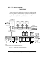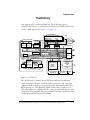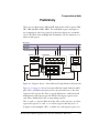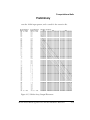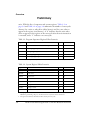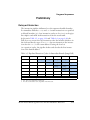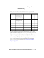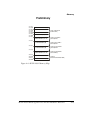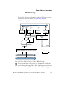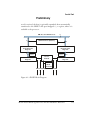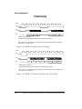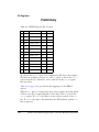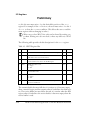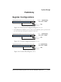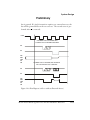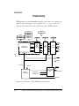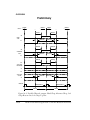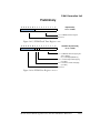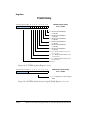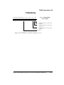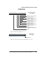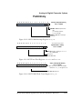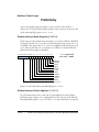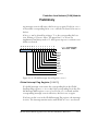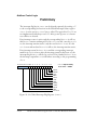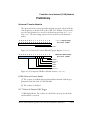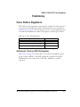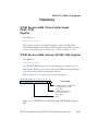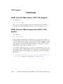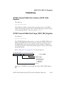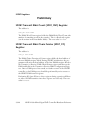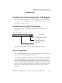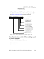
1
Preliminary ADSP-2199x Mixed Signal DSP Controller Hardware Reference Preliminary Revision 0, 2003 Part Number: 82-000640-01 Analog Devices, Inc. Digital Signal Processor Division One Technology Way Norwood, Mass. 02062-9106 Preliminary Copyright Information © 03 Analog Devices, Inc., ALL RIGHTS RESERVED. This document may not be reproduced in any form without prior, express written consent from Analog Devices, Inc. Printed in the USA. Disclaimer Analog Devices, Inc. reserves the right to change this product without prior notice. Information furnished by Analog Devices is believed to be accurate and reliable. However, no responsibility is assumed by Analog Devices for its use; nor for any infringement of patents or other rights of third parties which may result from its use. No license is granted by implication or otherwise under the patent rights of Analog Devices, Inc. Trademark and Service Mark Notice The Analog Devices logo, EZ-ICE, EZ-LAB, SHARC, the SHARC logo, TigerSHARC, the TigerSHARC logo, VisualDSP, and the VisualDSP logo are registered trademarks of Analog Devices, Inc. Apex-ICE, Blackfin, the Blackfin logo, CROSSCORE, the CROSSCORE logo, EZ-KIT Lite, ICEPAC, Mountain-ICE, SHARCPAC, Summit-ICE, Trek-ICE, VisualDSP++ and the VisualDSP++ logo are trademarks of Analog Devices, Inc. All other brand and product names are trademarks or service marks of their respective owners. CONTENTS Preliminary CONTENTS PREFACE Purpose ...................................................................................... xxxiii Instruction Set Enhancements ............................................... xxxiii For more Information about Analog Products ............................. xxxiv For Technical or Customer Support ............................................ xxxv What’s New in this Manual ......................................................... xxxv Related Documents .................................................................... xxxvi Conventions ............................................................................. xxxvii INTRODUCTION Overview—Why Fixed-Point DSP? ............................................... 1-1 ADSP-2199x Design Advantages ................................................... 1-2 ADSP-2199x Architecture Overview .............................................. 1-6 DSP Core Architecture ............................................................ 1-9 DSP Peripherals Architecture ................................................. 1-11 Memory Architecture ............................................................ 1-12 Internal (On-chip) Memory .............................................. 1-13 ADSP-2199x Mixed Signal DSP Controller Hardware Reference iii CONTENTS Preliminary External (Off-chip) Memory ............................................. 1-14 Interrupts ............................................................................. 1-16 DMA Controller ................................................................... 1-16 DSP Serial Port (SPORT) ..................................................... 1-17 Serial Peripheral Interface (SPI) Port ...................................... 1-18 Controller Area Network (CAN) Module ............................... 1-18 Analog To Digital Conversion System .................................... 1-19 PWM Generation Unit ......................................................... 1-20 Auxiliary PWM Generation Unit ........................................... 1-20 Encoder Interface Unit .......................................................... 1-21 Flag I/O (FIO) Peripheral Unit ............................................. 1-22 Low-Power Operation ........................................................... 1-22 Clock Signals ........................................................................ 1-23 Booting Modes ..................................................................... 1-23 JTAG Port ............................................................................ 1-24 Development Tools ..................................................................... 1-24 Differences from Previous DSPs .................................................. 1-27 Computational Units and Data Register File .......................... 1-27 Arithmetic Status (ASTAT) Register Latency .......................... 1-27 Norm and Exp Instruction Execution .................................... 1-27 Shifter Result (SR) Register as Multiplier Dual Accumulator .. 1-28 Shifter Exponent (SE) Register is not Memory Accessible ....... 1-28 Conditions (SWCOND) and Condition Code (CCODE) Register . 1-29 Unified Memory Space .......................................................... 1-30 iv ADSP-2199x Mixed Signal DSP Controller Hardware Reference CONTENTS Preliminary Data Memory Page (DMPG1 and DMPG2) Registers ............ 1-30 Data Address Generator (DAG) Addressing Modes ................. 1-31 Base Registers for Circular Buffers .......................................... 1-31 Program Sequencer, Instruction Pipeline, and Stacks .............. 1-32 Conditional Execution (Difference in Flag Input Support) ...... 1-32 Execution Latencies (Different for JUMP Instructions) ........... 1-33 COMPUTATIONAL UNITS Overview ...................................................................................... 2-1 Using Data Formats ...................................................................... 2-4 Binary String ........................................................................... 2-5 Unsigned ................................................................................. 2-5 Signed Numbers: Two’s Complement ....................................... 2-5 Signed Fractional Representation: 1.15 .................................... 2-5 ALU Data Types ...................................................................... 2-6 Multiplier Data Types .............................................................. 2-7 Shifter Data Types ................................................................... 2-8 Arithmetic Formats Summary .................................................. 2-8 Setting Computational Modes ..................................................... 2-10 Latching ALU Result Overflow Status .................................... 2-10 Saturating ALU Results on Overflow ...................................... 2-11 Using Multiplier Integer and Fractional Formats .................... 2-11 Rounding Multiplier Results .................................................. 2-13 Unbiased Rounding .......................................................... 2-14 Biased Rounding ............................................................... 2-15 ADSP-2199x Mixed Signal DSP Controller Hardware Reference v CONTENTS Preliminary Using Computational Status ....................................................... 2-16 Arithmetic Logic Unit (ALU) ...................................................... 2-17 ALU Operation ..................................................................... 2-17 ALU Status Flags ................................................................... 2-18 ALU Instruction Summary .................................................... 2-19 ALU Data Flow Details ......................................................... 2-21 ALU Division Support Features ............................................. 2-24 Multiply—Accumulator (Multiplier) ........................................... 2-29 Multiplier Operation ............................................................. 2-29 Placing Multiplier Results in MR or SR Registers .............. 2-31 Clearing, Rounding, or Saturating Multiplier Results ......... 2-32 Multiplier Status Flags ........................................................... 2-33 Saturating Multiplier Results on Overflow ............................. 2-33 Multiplier Instruction Summary ............................................ 2-35 Multiplier Data Flow Details ................................................. 2-37 Barrel-Shifter (Shifter) ................................................................ 2-39 Shifter Operations ................................................................. 2-39 Derive Block Exponent ..................................................... 2-41 Immediate Shifts .............................................................. 2-42 Denormalize ..................................................................... 2-45 Normalize, Single-Precision Input ..................................... 2-47 Normalize, ALU Result Overflow ...................................... 2-48 Normalize, Double-Precision Input ................................... 2-50 Shifter Status Flags ................................................................ 2-53 vi ADSP-2199x Mixed Signal DSP Controller Hardware Reference CONTENTS Preliminary Shifter Instruction Summary .................................................. 2-54 Shifter Data Flow Details ....................................................... 2-55 Data Register File ........................................................................ 2-61 Secondary (Alternate) Data Registers ........................................... 2-63 Multifunction Computations ...................................................... 2-64 PROGRAM SEQUENCER Overview ...................................................................................... 3-1 Instruction Pipeline ...................................................................... 3-7 Instruction Cache ....................................................................... 3-10 Using the Cache .................................................................... 3-13 Optimizing Cache Usage ....................................................... 3-13 Branches and Sequencing ............................................................ 3-15 Indirect Jump Page (IJPG) Register ........................................ 3-18 Conditional Branches ............................................................ 3-18 Delayed Branches .................................................................. 3-19 Loops and Sequencing ................................................................. 3-23 Managing Loop Stacks ........................................................... 3-26 Restrictions on Ending Loops ................................................ 3-26 Interrupts and Sequencing ........................................................... 3-26 Stacks and Sequencing ................................................................ 3-32 Conditional Sequencing .............................................................. 3-37 Sequencer Instruction Summary .................................................. 3-40 ADSP-2199x Mixed Signal DSP Controller Hardware Reference vii CONTENTS Preliminary MEMORY Overview ...................................................................................... 4-1 Internal Address and Data Buses .............................................. 4-6 External Address and Data Buses ............................................. 4-7 Internal Data Bus Exchange .................................................... 4-8 ADSP-2199x Memory Organization ........................................... 4-11 Shadow Write FIFO .............................................................. 4-16 Data Move Instruction Summary ................................................ 4-17 DATA ADDRESS GENERATORS Overview ...................................................................................... 5-1 Setting DAG Modes ..................................................................... 5-4 Secondary (Alternate) DAG Registers ...................................... 5-4 Bit-Reverse Addressing Mode .................................................. 5-6 DAG Page Registers (DMPGx) ................................................ 5-7 Using DAG Status ........................................................................ 5-8 DAG Operations .......................................................................... 5-9 Addressing with DAGs ............................................................ 5-9 Addressing Circular Buffers ................................................... 5-12 Addressing with Bit-Reversed Addresses ................................. 5-16 Modifying DAG Registers ..................................................... 5-20 DAG Register Transfer Restrictions ............................................. 5-20 DAG Instruction Summary ......................................................... 5-22 viii ADSP-2199x Mixed Signal DSP Controller Hardware Reference CONTENTS Preliminary I/O PROCESSOR Overview ...................................................................................... 6-1 Descriptor-Based DMA Transfers ............................................. 6-5 Autobuffer-Based DMA Transfers ............................................ 6-8 Interrupts from DMA Transfers ............................................... 6-9 Setting Peripheral DMA Modes ................................................... 6-10 MemDMA DMA Settings ...................................................... 6-14 Serial Port DMA Settings ....................................................... 6-15 SPI Port DMA Settings .......................................................... 6-16 Working with Peripheral DMA Modes ......................................... 6-17 Using MemDMA DMA ......................................................... 6-17 Using Serial Port (SPORT) DMA .......................................... 6-18 Descriptor-Based SPORT DMA ........................................ 6-18 Autobuffer-Based SPORT DMA ........................................ 6-19 SPORT DMA Data Packed/Unpacked Enable ................... 6-20 Using Serial Peripheral Interface (SPI) Port DMA ................... 6-21 SPI DMA in Master Mode ................................................ 6-21 SPI DMA in Slave Mode ................................................... 6-23 SPI DMA Errors ............................................................... 6-25 Boot Mode DMA Transfers ......................................................... 6-27 Code Example: Internal Memory DMA ....................................... 6-28 EXTERNAL PORT Overview ...................................................................................... 7-1 ADSP-2199x Mixed Signal DSP Controller Hardware Reference ix CONTENTS Preliminary Setting External Port Modes .......................................................... 7-3 Memory Bank and Memory Space Settings .............................. 7-3 External Bus Settings ............................................................... 7-5 Bus Master Settings ................................................................. 7-7 Boot Memory Space Settings ................................................... 7-7 Working with External Port Modes ............................................... 7-8 Using Memory Bank/Space Waitstates Modes .......................... 7-9 Using Memory Bank/Space Clock Modes .............................. 7-10 Using External Memory Banks and Pages ............................... 7-11 Using Memory Access Status ................................................. 7-11 Using Bus Master Modes ....................................................... 7-12 Using Boot Memory Space .................................................... 7-14 Reading from Boot Memory ............................................. 7-14 Writing to Boot Memory .................................................. 7-15 Interfacing to External Memory .................................................. 7-15 Data Alignment—Logical versus Physical Address .................. 7-15 Memory Interface Pins .......................................................... 7-20 Memory Interface Timing ..................................................... 7-24 Code Example: BMS Runtime Access .......................................... 7-28 SERIAL PORT Overview ...................................................................................... 8-1 SPORT Operation .................................................................. 8-6 SPORT Disable ...................................................................... 8-7 Setting SPORT Modes .................................................................. 8-8 x ADSP-2199x Mixed Signal DSP Controller Hardware Reference CONTENTS Preliminary Transmit and Receive Configuration Registers (SP_TCR, SP_RCR) 8-10 Register Writes and Effect Latency ......................................... 8-16 Transmit and Receive Data Buffers (SP_TX, SP_RX) ............. 8-17 Clock and Frame Sync Frequencies ........................................ 8-18 Maximum Clock Rate Restrictions .................................... 8-20 Frame Sync and Clock Example ......................................... 8-20 Data Word Formats ............................................................... 8-20 Word Length .................................................................... 8-21 Endian Format .................................................................. 8-21 Data Type ......................................................................... 8-21 Companding ..................................................................... 8-22 Clock Signal Options ............................................................ 8-22 Frame Sync Options .............................................................. 8-23 Framed versus Unframed ................................................... 8-23 Internal versus External Frame Syncs ................................. 8-25 Active Low versus Active High Frame Syncs ....................... 8-26 Sampling Edge for Data and Frame Syncs .......................... 8-26 Early versus Late Frame Syncs (Normal and Alternate Timing) 8-27 Data-Independent Transmit Frame Sync ............................ 8-29 Multichannel Operation ........................................................ 8-29 Frame Syncs in Multichannel Mode ................................... 8-32 Multichannel Frame Delay ................................................ 8-33 Window Size ..................................................................... 8-33 Window Offset ................................................................. 8-33 ADSP-2199x Mixed Signal DSP Controller Hardware Reference xi CONTENTS Preliminary Other Multichannel Fields in SP_TCR, SP_RCR .............. 8-34 Channel Selection Registers .............................................. 8-35 Multichannel Enable ......................................................... 8-36 Multichannel DMA Data Packing ..................................... 8-36 Multichannel Mode Example ............................................ 8-37 Moving Data Between SPORTS and Memory ............................. 8-38 SPORT DMA Autobuffer Mode Example .............................. 8-39 SPORT Descriptor-Based DMA Example .............................. 8-40 Support for Standard Protocols ................................................... 8-42 2X Clock Recovery Control ................................................... 8-43 SPORT Pin/Line Terminations ................................................... 8-43 Timing Examples ........................................................................ 8-43 SERIAL PERIPHERAL INTERFACE (SPI) PORT Overview ...................................................................................... 9-1 Interface Signals ........................................................................... 9-4 Serial Peripheral Interface Clock Signal (SCK) ......................... 9-5 Serial Peripheral Interface Slave Select Input Signal (SPISS) ..... 9-5 Master Out Slave In (MOSI) ................................................... 9-6 Master In Slave Out (MISO) ................................................... 9-6 Interrupt Behavior .................................................................. 9-7 SPI Registers ................................................................................ 9-8 SPI Baud Rate (SPIBAUD) Register ....................................... 9-8 SPI Control (SPICTL) Register ............................................... 9-9 SPI Flag (SPIFLG) Register ................................................... 9-11 xii ADSP-2199x Mixed Signal DSP Controller Hardware Reference CONTENTS Preliminary Slave-Select Inputs ............................................................ 9-13 Use of FLS Bits in SPIFLG for Multiple-Slave SPI Systems 9-13 SPI Status (SPIST) Register ................................................... 9-15 Transmit Data Buffer (TDBR) Register .................................. 9-17 Receive Data Buffer (RDBR) Register .................................... 9-17 Data Shift (SFDR) Register ................................................... 9-18 Register Mapping .................................................................. 9-18 SPI Transfer Formats ................................................................... 9-19 SPI General Operation ................................................................ 9-22 Clock Signals ........................................................................ 9-23 Master Mode Operation ........................................................ 9-24 Transfer Initiation from Master (Transfer Modes) ................... 9-26 Slave Mode Operation ....................................................... 9-26 Slave Ready for a Transfer .................................................. 9-28 Error Signals and Flags ................................................................ 9-28 Mode-Fault Error (MODF) ................................................... 9-28 Transmission Error (TXE) Bit ................................................ 9-30 Reception Error (RBSY) Bit ................................................... 9-30 Transmit Collision Error (TXCOL) Bit .................................. 9-30 Beginning and Ending of an SPI Transfer .................................... 9-31 DMA .......................................................................................... 9-32 TIMER Overview .................................................................................... 10-1 Pulsewidth Modulation (PWMOUT) Mode ........................... 10-7 ADSP-2199x Mixed Signal DSP Controller Hardware Reference xiii CONTENTS Preliminary PWM Waveform Generation ............................................ 10-8 Single-Pulse Generation .................................................. 10-11 Pulsewidth Count and Capture (WDTH_CAP) Mode ......... 10-11 External Event Watchdog (EXT_CLK) Mode ...................... 10-14 Code Examples ......................................................................... 10-14 Timer Example Steps .......................................................... 10-15 Timer0 Initialization Routine .............................................. 10-18 Timer Interrupt Routine ..................................................... 10-20 JTAG TEST-EMULATION PORT Overview .................................................................................... 11-1 JTAG Test Access Port ................................................................ 11-2 INSTRUCTION Register ........................................................... 11-3 BYPASS Register ........................................................................ 11-4 BOUNDARY Register ................................................................ 11-4 IDCODE Register ...................................................................... 11-4 References .................................................................................. 11-5 SYSTEM DESIGN Overview .................................................................................... 12-1 Pin Descriptions ......................................................................... 12-1 Recommendations for Unused Pins ....................................... 12-5 Pin States at Reset ....................................................................... 12-6 Resetting the Processor (“Hard Reset”) ...................................... 12-10 Resetting the Processor (“Soft Reset”) ........................................ 12-11 xiv ADSP-2199x Mixed Signal DSP Controller Hardware Reference CONTENTS Preliminary Booting the Processor (“Boot Loading”) .................................... 12-13 Booting Modes .................................................................... 12-13 Boot from External 8-Bit Memory (EPROM) over EMI ... 12-13 Execute from External 8-Bit Memory .............................. 12-14 Execute from External 16-Bit Memory ............................ 12-14 Boot from SPI0 with < 4k bits ......................................... 12-14 Boot from SPI0 with > 4k bits ......................................... 12-15 Bootstream Format .............................................................. 12-15 Managing DSP Clocks .............................................................. 12-21 Phase Locked Loop (PLL) ......................................................... 12-23 Clock Generation (CKGEN) Module ........................................ 12-25 Overview of CKGEN Functionality ..................................... 12-25 Hardware Reset Generation ................................................. 12-26 Software Reset Logic ............................................................ 12-27 Clock Generation & PLL Control ........................................ 12-28 Lock Counter ...................................................................... 12-31 Powerdown Control/Modes ....................................................... 12-32 Idle Mode ........................................................................... 12-32 Powerdown Core Mode ....................................................... 12-33 Powerdown Core/Peripherals Mode ...................................... 12-33 Powerdown All Mode .......................................................... 12-34 Register Configurations ............................................................. 12-35 Working with External Bus Masters ........................................... 12-36 Recommended Reading ............................................................. 12-40 ADSP-2199x Mixed Signal DSP Controller Hardware Reference xv CONTENTS Preliminary PERIPHERAL INTERRUPT CONTROLLER Overview .................................................................................... 13-1 ADSP-2199x PERIPHERAL INTERRUPT CONTROLLER ...... 13-2 GENERAL OPERATION .......................................................... 13-3 REGISTERS .............................................................................. 13-5 WATCHDOG TIMER Overview .................................................................................... 14-1 General Operation ...................................................................... 14-1 Registers ..................................................................................... 14-3 POWER ON RESET Overview .................................................................................... 15-1 ENCODER INTERFACE UNIT Overview .................................................................................... 16-1 Encoder Loop Timer .................................................................. 16-4 Encoder Interface Structure & Operation .................................... 16-5 Introduction ......................................................................... 16-5 Programmable Input Noise Filtering of Encoder Signals ......... 16-5 Encoder Counter Direction ................................................... 16-9 Alternative Frequency and Direction Inputs ......................... 16-10 Encoder Counter Reset ....................................................... 16-10 Registration Inputs & Software Zero Marker ....................... 16-12 Single North Marker Mode ................................................. 16-14 xvi ADSP-2199x Mixed Signal DSP Controller Hardware Reference CONTENTS Preliminary Encoder Error Checking ...................................................... 16-14 EIU Input Pin Status ........................................................... 16-14 Interrupts ............................................................................ 16-15 32-bit Register Accesses ....................................................... 16-15 Encoder Event Timer ................................................................ 16-17 Introduction & Overview .................................................... 16-17 Latching Data from the EET ............................................... 16-18 EET Status Register ............................................................. 16-20 EIU/EET Registers ................................................................... 16-21 Inputs/Outputs ......................................................................... 16-27 AUXILIARY PWM GENERATION UNIT Overview .................................................................................... 17-1 Independent Mode ...................................................................... 17-2 Offset Mode ............................................................................... 17-4 Operation Features ...................................................................... 17-5 AUXTRIP Shutdown .................................................................. 17-6 AUXSYNC Operation ................................................................. 17-7 Registers ..................................................................................... 17-8 PWM GENERATION UNIT OVERVIEW ............................................................................... 18-1 GENERAL OPERATION ..................................................... 18-7 FUNCTIONAL DESCRIPTION .......................................... 18-8 Three-Phase Timing & Dead Time Insertion Unit ............. 18-8 ADSP-2199x Mixed Signal DSP Controller Hardware Reference xvii CONTENTS Preliminary PWM Switching Frequency, PWMTM Register ................. 18-8 PWM Switching Dead Time, PWMDT Register ............... 18-9 PWM Operating Mode, PWMCTRL & PWMSTAT Registers .. 18-10 PWM Duty Cycles, PWMCHA, PWMCHB, PWMCHC Registers 18-12 Special Consideration for PWM Operation in Over-Modulation 18-16 PWM Timer Operation .................................................. 18-19 Effective PWM Accuracy ................................................ 18-20 Switched Reluctance Mode ............................................. 18-21 Output Control Unit ...................................................... 18-21 Crossover Feature ........................................................... 18-22 Output Enable Function ................................................. 18-22 Brushless DC Motor (Electronically Commutated Motor) Control 18-23 GATE DRIVE UNIT ......................................................... 18-25 High Frequency Chopping .............................................. 18-25 PWM Polarity Control, PWMPOL Pin ........................... 18-26 Output Control Feature Precedence ................................ 18-27 Switched Reluctance Mode ............................................. 18-27 PWMSYNC Operation ................................................... 18-31 Internal PWMSYNC generation ..................................... 18-31 External PWMSYNC operation ...................................... 18-31 PWM Shutdown & Interrupt Control Unit ..................... 18-32 xviii ADSP-2199x Mixed Signal DSP Controller Hardware Reference CONTENTS Preliminary Registers ................................................................................... 18-33 ANALOG TO DIGITAL CONVERTER SYSTEM Overview .................................................................................... 19-1 ADC Inputs ................................................................................ 19-2 Analog to Digital Converter and Input Structure ......................... 19-2 ADC Control Module ................................................................. 19-6 ADC Clock ........................................................................... 19-6 ADC Data Formats ............................................................... 19-7 Convert Start Trigger ............................................................. 19-8 ADC Time Counters ............................................................. 19-9 Conversion Modes ............................................................... 19-10 Simultaneous Sampling Mode ......................................... 19-11 Latch Mode .................................................................... 19-12 Offset Calibration Mode ................................................. 19-12 DMA Single Channel Acquisition Mode .......................... 19-13 DMA Dual Channel Acquisition Mode ........................... 19-14 DMA Quad Channel Acquisition Mode .......................... 19-14 DMA Octal Channel Acquisition Mode ........................... 19-15 DMA Operation Overview .................................................. 19-15 Voltage Reference ...................................................................... 19-16 Registers ................................................................................... 19-17 FLAG I/O (FIO) PERIPHERAL UNIT Overview .................................................................................... 20-1 ADSP-2199x Mixed Signal DSP Controller Hardware Reference xix CONTENTS Preliminary Operation of the FIO Block ........................................................ 20-3 Flag Register ......................................................................... 20-3 Flag as Output ...................................................................... 20-3 Flag as Input ......................................................................... 20-4 Interrupt Outputs ................................................................. 20-4 Flag Wake-up output ............................................................ 20-5 FIO Lines as PWM Shutdown Sources. ................................. 20-5 FIO Lines as SPI Slave Select Lines ........................................ 20-6 Configuration Registers ......................................................... 20-6 Flag Configuration Registers ................................................. 20-7 FIO Direction Control (DIR) Register .............................. 20-8 Flag Control (FLAGC and FLAGS) Registers .................... 20-8 Flag Interrupt Mask (MASKAC, MASKAS, MASKBC, and MASKBS) Registers ....................................................... 20-8 FIO Polarity Control (POLAR) Register ........................... 20-9 FIO Edge/Level Sensitivity Control (EDGE and BOTH) Registers 20-10 Power-Down Modes ............................................................ 20-10 Idle Mode ...................................................................... 20-11 Power-Down Core Mode ................................................ 20-11 Power-Down Core/Peripherals Mode ............................... 20-12 Power-Down All Mode ................................................... 20-13 Reset State .......................................................................... 20-13 Registers ................................................................................... 20-14 xx ADSP-2199x Mixed Signal DSP Controller Hardware Reference CONTENTS Preliminary CONTROLLER AREA NETWORK (CAN) MODULE Overview .................................................................................... 21-1 CAN Module Registers ............................................................... 21-4 Master Control Register (CANMCR) ..................................... 21-4 CCR CAN Configuration Mode Request ........................... 21-4 CSR CAN Suspend Mode Request .................................... 21-5 SMR Sleep Mode Request ................................................. 21-6 WBA Wake Up on CAN Bus Activity ................................ 21-6 TxPrio Transmit Priority by message identifier (if implemented) ............................................................ 21-6 ABO Auto Bus On ............................................................ 21-6 DNM Device Net Mode (if implemented) ......................... 21-7 SRS Software Reset ........................................................... 21-7 Global Status Register (CANGSR) ......................................... 21-8 Rec Receive Mode ............................................................. 21-9 Trm Transmit Mode .......................................................... 21-9 MBptr Mail Box Pointer ................................................... 21-9 CCA CAN Configuration Mode Acknowledge ................... 21-9 CSA CAN Suspend Mode Acknowledge ............................ 21-9 SMA Sleep Mode Acknowledge ....................................... 21-10 EBO CAN Error Bus Off Mode ...................................... 21-10 EP CAN Error Passive Mode ........................................... 21-10 WR CAN Receive Warning Flag ...................................... 21-10 WT CAN Transmit Warning Flag .................................... 21-10 ADSP-2199x Mixed Signal DSP Controller Hardware Reference xxi CONTENTS Preliminary CAN Configuration Registers ................................................... 21-11 Bit Configuration Register 0 (CANBCR0) ........................... 21-12 Bit Configuration Register 1 (CANBCR1) ........................... 21-13 CAN Configuration Register (CANCNF) ............................ 21-13 TEST Enable for the special functions ............................ 21-14 MRB Mode Read Back ................................................... 21-14 MAA Mode Auto Acknowledge ....................................... 21-15 DIL Disable CAN Internal Loop ..................................... 21-15 DTO Disable CAN TX Output ...................................... 21-15 DRI Disable CAN RX Input ........................................... 21-15 DEC Disable CAN Error Counter .................................. 21-15 Version Code Register (CANVERSION) ............................. 21-16 CAN Error Counter Register (CANCEC) ............................ 21-16 Interrupt Register (CANINTR) ........................................... 21-17 Rx Serial Input from CAN Bus Line (from Transceiver) ... 21-18 TX Serial Output to CAN Bus Line (to Transceiver) ........ 21-18 SMACK Sleep Mode Acknowledge .................................. 21-19 GIRQ Global Interrupt Output ...................................... 21-19 MBTIF Mailbox Transmit Interrupt Output ................... 21-19 MBRIF Mailbox Receive Interrupt Output ..................... 21-19 Data Storage ............................................................................. 21-20 Mailbox Layout ................................................................... 21-21 Mailbox Area ...................................................................... 21-23 Mailbox Types .................................................................... 21-24 xxii ADSP-2199x Mixed Signal DSP Controller Hardware Reference CONTENTS Preliminary Mailbox Control Logic .............................................................. 21-24 Mailbox Configuration (CANMC / CANMD) ..................... 21-24 Receive Logic ...................................................................... 21-26 Acceptance Filter / Data Acceptance Filter ............................ 21-27 Acceptance Mask Register .................................................... 21-29 FDF Filtering on Data Field (if enabled) .......................... 21-30 FMD Full Mask Data Field ............................................. 21-30 AMIDE Acceptance Mask Identifier Extension ................ 21-31 BaseId Base Identifier ...................................................... 21-31 ExtId Extended Identifier ................................................ 21-31 DFM Data Field Mask .................................................... 21-31 Receive Control Registers .................................................... 21-31 Receive Message Pending Register (CANRMP) ................ 21-31 Receive Message Lost Register (CANRML) ...................... 21-32 Overwrite Protection / Single Shot Transmission Register (CANOPSS) ................................................................ 21-32 Transmit Logic ................................................................ 21-33 Retransmission ................................................................ 21-34 Single Shot Transmission ................................................. 21-35 Transmit Priority defined by Mailbox Number ................. 21-35 Transmit Control Registers .............................................. 21-35 Transmission Request Set Register (CANTRS) ................. 21-36 Transmission Request Reset Register (CANTRR) ............. 21-36 Abort Acknowledge Register (CANAA) ............................ 21-38 Transmission Acknowledge Register (CANTA) ................. 21-39 ADSP-2199x Mixed Signal DSP Controller Hardware Reference xxiii CONTENTS Preliminary Temporary Mailbox Disable Feature (CANMBTD) ......... 21-39 Remote Frame Handling Register (CANRFH) ................. 21-41 Mailbox Interrupts .............................................................. 21-43 Mailbox Interrupt Mask Register (CANMBIM) .............. 21-43 Mailbox Transmit Interrupt Flag Register (CANMBTIF) . 21-44 Mailbox Receive Interrupt Flag Register (CANMBRIF) ... 21-45 Global Interrupt ................................................................. 21-46 ADI Access Denied Interrupt .......................................... 21-46 EXTI External Trigger Output Interrupt ......................... 21-46 UCE Universal Counter Event ........................................ 21-47 RMLI Receive Message Lost Interrupt ............................. 21-47 AAI Abort Acknowledge Interrupt .................................. 21-47 UIAI Access to Unimplemented Address Interrupt ........... 21-48 WUI Wake Up Interrupt ................................................ 21-48 BOI Bus-Off Interrupt ................................................... 21-48 EPI Error-Passive Interrupt ............................................. 21-48 EWRI Error Warning Receive Interrupt .......................... 21-49 EWTI Error Warning Transmit Interrupt ........................ 21-49 Global Interrupt Logic .................................................... 21-49 Global Interrupt Mask Register (CANGIM) .................... 21-50 Global Interrupt Status Register (CANGIS) .................... 21-50 Global Interrupt Flag Register (CANGIF) ....................... 21-51 Universal Counter Module .............................................. 21-53 UCEN Universal Counter Enable ............................... 21-53 xxiv ADSP-2199x Mixed Signal DSP Controller Hardware Reference CONTENTS Preliminary UCCT Universal Counter CAN Trigger ....................... 21-53 UCRC Universal Counter Reload / Clear ..................... 21-54 UCCNF Universal Counter Mode ............................... 21-54 Event Counter Modes ................................................. 21-55 Time Stamp Counter Mode ............................................. 21-56 Error Status Register (CANESR) ..................................... 21-57 FER Form Error Flag ...................................................... 21-57 BEF Bit Error Flag .......................................................... 21-57 SA1 Stuck at dominant Error .......................................... 21-58 CRCE CRC Error ........................................................... 21-58 SER Stuff Error ............................................................... 21-58 ACKE Acknowledge Error ............................................... 21-58 Programmable Warning Limit for REC and TEC ............. 21-58 ADSP-2199X DSP CORE REGISTERS Overview .................................................................................... 22-1 Core Registers Summary ........................................................ 22-2 Register Load Latencies ......................................................... 22-4 Core Status Registers ................................................................... 22-7 Arithmetic Status (ASTAT) Register ....................................... 22-7 Mode Status (MSTAT) Register ............................................. 22-8 System Status (SSTAT) Register ........................................... 22-10 Computational Unit Registers ................................................... 22-11 Data Register File (Dreg) Registers ....................................... 22-11 ALU X- & Y-Input (AX0, AX1, AY0, AY1) Registers ............ 22-12 ADSP-2199x Mixed Signal DSP Controller Hardware Reference xxv CONTENTS Preliminary ALU Results (AR) Register .................................................. 22-12 ALU Feedback (AF) Register ............................................... 22-12 Multiplier X- & Y-Input (MX0, MX1, MY0, MY1) Registers 22-12 Multiplier Results (MR2, MR1, MR0) Registers .................. 22-13 Shifter Input (SI) Register ................................................... 22-13 Shifter Exponent (SE) & Block Exponent (SB) Registers ...... 22-13 Shifter Results (SR2, SR1, SR0) Registers ............................ 22-13 Program Sequencer Registers ..................................................... 22-14 Interrupt Mask (IMASK) & Latch (IRPTL) Registers .......... 22-15 Interrupt Control (ICNTL) Register .................................... 22-16 Indirect Jump Page (IJPG) Register ..................................... 22-16 PC Stack Page (STACKP) and PC Stack Address (STACKA) Registers ............................. 22-17 Loop Stack Page (LPSTACKP) and Loop Stack Address (LPSTACKA) Register ....................... 22-17 Counter (CNTR) Register ................................................... 22-18 Condition Code (CCODE) Register .................................... 22-18 Cache Control (CACTL) Register ....................................... 22-20 Data Address Generator Registers .............................................. 22-20 Index (Ix) Registers ............................................................. 22-21 Modify (Mx) Registers ........................................................ 22-21 Length and Base (Lx,Bx) Register ........................................ 22-21 Data Memory Page (DMPGx) Registers ............................... 22-22 Memory Interface Registers ....................................................... 22-22 PM Bus Exchange (PX) Register .......................................... 22-22 xxvi ADSP-2199x Mixed Signal DSP Controller Hardware Reference CONTENTS Preliminary I/O Memory Page (IOPG) Register ...................................... 22-22 Register & Bit #Defines File (def219x.h) ................................... 22-23 ADSP-2199X DSP I/O REGISTERS Overview .................................................................................... 23-1 I/O Processor (Memory Mapped) Registers .................................. 23-2 Clock and System Control Registers .......................................... 23-11 PLL Control (PLLCTL) Register ......................................... 23-11 PLL Lock Counter (LOCKCNT) Register ............................ 23-12 Software Reset (SWRST) Register ...................................... 23-13 Next System Configuration (NXTSCR) Register .................. 23-14 System Configuration (SYSCR) Register .............................. 23-15 DMA Controller Registers ......................................................... 23-16 DMA, MemDMA Channel Write Pointer (DMACW_PTR) Register 23-16 DMA, MemDMA Channel Write Configuration (DMACW_CFG) Register ............................................................................ 23-17 DMA, MemDMA Channel Write Start Page (DMACW_SRP) Register 23-19 DMA, MemDMA Channel Write Start Address (DMACW_SRA) Register ............................................................................ 23-19 DMA, MemDMA Channel Write Count (DMACW_CNT) Register 23-19 DMA, MemDMA Channel Write Chain Pointer (DMACW_CP) Register ............................................................................ 23-20 DMA, MemDMA Channel Write Chain Pointer Ready (DMACW_CPR) Register ................................................ 23-20 ADSP-2199x Mixed Signal DSP Controller Hardware Reference xxvii CONTENTS Preliminary DMA, MemDMA Channel Write Interrupt (DMACW_IRQ) Register 23-20 DMA, MemDMA Channel Read Pointer (DMACR_PTR) Register 23-21 DMA, MemDMA Channel Read Configuration (DMACR_CFG) Register ............................................................................ 23-21 DMA, MemDMA Channel Read Start Page (DMACR_SRP) Register 23-22 DMA, MemDMA Channel Read Start Address (DMACR_SRA) Register ............................................................................ 23-22 DMA, MemDMA Channel Read Count (DMACR_CNT) Register 23-22 DMA, MemDMA Channel Read Chain Pointer (DMACR_CP) Register 23-23 DMA, MemDMA Channel Read Chain Pointer Ready (DMACR_CPR) Register ............................................................................ 23-23 DMA, MemDMA Channel Read Interrupt (DMACR_IRQ) Register 23-23 SPORT Registers ...................................................................... 23-24 SPORT Transmit Configuration (SP_TCR) Register ............ 23-24 SPORT Receive Configuration (SP_RCR) Register .............. 23-28 SPORT Transmit Data (SP_TX) Register ............................ 23-29 SPORT Receive Data (SP_RX) Register ............................... 23-29 SPORT Transmit (SP_TSCKDIV) and (SP_RSCKDIV) Serial Clock Divider Registers ............................................................. 23-30 SPORT Transmit (SP_TFSDIV) and Receive (SP_RFSDIV) Frame Sync Divider Registers ...................................................... 23-31 SPORT Status (SP_STATR) Register ................................... 23-31 xxviii ADSP-2199x Mixed Signal DSP Controller Hardware Reference CONTENTS Preliminary SPORT Multi-Channel Transmit Select (SP_MTCSx) Registers 23-33 SPORT Multi-Channel Receive Select (SP_MRCSx) Registers 23-34 SPORT Multi-Channel Configuration (SP_MCMCx) Registers 23-35 SPORT DMA Receive Pointer (SPDR_PTR) Register .......... 23-39 SPORT Receive DMA Configuration (SPDR_CFG) Register 23-39 SPORT Receive DMA Start Page (SPDR_SRP) Register ....... 23-41 SPORT Receive DMA Start Address (SPDR_SRA) Register .. 23-41 SPORT Receive DMA Count (SPDR_CNT) Register .......... 23-42 SPORT Receive DMA Chain Pointer (SPDR_CP) Register .. 23-42 SPORT Receive DMA Chain Pointer Ready (SPDR_CPR) Register ............................................................................ 23-43 SPORT Receive DMA Interrupt (SPxDR_IRQ) Register ...... 23-43 SPORT Transmit DMA Pointer (SPDT_PTR) Register ........ 23-44 SPORT Transmit DMA Configuration (SPDT_CFG) Register 23-44 SPORT Transmit DMA Start Address (SPDT_SRA) Register 23-45 SPORT Transmit DMA Start Page (SPDT_SRP) Register .... 23-45 SPORT Transmit DMA Count (SPDT_CNT) Register ........ 23-46 SPORT Transmit DMA Chain Pointer (SPDT_CP) Register 23-46 SPORT Transmit DMA Chain Pointer Ready (SPDT_CPR) Register ............................................................................ 23-47 SPORT Transmit DMA Interrupt (SPDT_IRQ) Register ..... 23-47 Serial Peripheral Interface Registers ............................................ 23-48 SPI Control (SPICTL) Register ............................................ 23-48 SPI Flag (SPIFLG) Register ................................................. 23-51 SPI Status (SPIST) Register ................................................. 23-52 ADSP-2199x Mixed Signal DSP Controller Hardware Reference xxix CONTENTS Preliminary SPI Transmit Buffer (TDBR) Register ................................. 23-54 Receive Buffer, SPI (RDBR) Register ................................... 23-54 Receive Data Buffer Shadow, SPI (RDBRS) Register ............ 23-55 SPI Baud Rate (SPIBAUD) Register .................................... 23-55 SPI DMA Current Pointer (SPID_PTR) Register ................. 23-55 SPI DMA Configuration (SPID_CFG) Register ................... 23-56 SPI DMA Start Page (SPID_SRP) Register .......................... 23-58 SPI DMA Start Address (SPID_SRA) Register ..................... 23-58 SPI DMA Word Count (SPID_CNT) Register .................... 23-58 SPI DMA Next Chain Pointer (SPID_CP) Register ............. 23-58 SPI DMA Chain Pointer Ready (SPID_CPR) Register ......... 23-59 SPI DMA Interrupt (SPID_IRQ) Register ........................... 23-59 Timer Registers ........................................................................ 23-59 Timer Global Status and Control (T_GSRx) Registers ......... 23-60 Timer Configuration (T_CFGRx) Registers ......................... 23-62 Timer Counter, low word (T_CNTLx) and high word (T_CNTHx) Registers .......................................................................... 23-63 Timer Period, low word (T_PRDLx) and high word (T_PRDHx) Registers .......................................................................... 23-65 Timer Width, low word (T_WLRx) and high word (T_WHRx) Register 23-66 External Memory Interface Registers ......................................... 23-68 External Memory Interface Control/Status (E_STAT) Register 23-68 External Memory Interface Control (EMICTL) Register ...... 23-69 Boot Memory Select Control (BMSCTL) Register ............... 23-70 xxx ADSP-2199x Mixed Signal DSP Controller Hardware Reference CONTENTS Preliminary Memory Select Control (MSxCTL) Registers ....................... 23-72 I/O Memory Select Control (IOMSCTL) Register .............. 23-73 External Port Status (EMISTAT) Register ............................. 23-73 Memory Page (MEMPGx) Registers ..................................... 23-75 NUMERIC FORMATS Overview .................................................................................... 24-1 Un/Signed: Two’s-Complement Format ....................................... 24-1 Integer or Fractional .................................................................... 24-2 Binary Multiplication .................................................................. 24-4 Fractional Mode and Integer Mode ........................................ 24-5 Block Floating-Point Format ....................................................... 24-6 INDEX ADSP-2199x Mixed Signal DSP Controller Hardware Reference xxxi Preliminary -xxxii ADSP-2199x Mixed Signal DSP Controller Hardware Reference Preface Preliminary PREFACE Purpose The ADSP-2199x Mixed Signal DSP Controller Hardware Reference provides architectural information on the ADSP-2199x family of DSP products and the ADSP-219x modified Harvard architecture Digital Signal Processor (DSP) core. The architectural descriptions cover functional blocks, buses, and ports, including all the features and processes they support. Instruction Set Enhancements The ADSP-2199x provides near source code compatibility with the previous family members, easing the process of porting code. All computational instructions (but not all registers) from previous ADSP-2100 family DSPs ADSP-2199x Mixed Signal DSP Controller Hardware Reference xxxiii For more Information about Analog Products Preliminary are available in the ADSP-2199x. New instructions, control registers, or other facilities, required to support the new feature set of the ADSP-219x core are: • Program flow control differences (pipeline execution and changes to looping) • Memory accessing differences (DAG support and memory map) • Peripheral I/O differences (additional ports and added DMA functionality) For programming information, see the ADSP-219x DSP Instruction Set Reference. For more Information about Analog Products Analog Devices is online on the internet at http://www.analog.com. Our Web pages provide information on the company and products, including access to technical information and documentation, product overviews, and product announcements. You may also obtain additional information about Analog Devices and its products in any of the following ways: Visit our World Wide Web site at www.analog.com • FAX questions or requests for information to 1(781)461-3010. • Access the DSP Division File Transfer Protocol (FTP) site at ftp ftp.analog.com or ftp 137.71.23.21 or ftp://ftp.analog.com. xxxiv ADSP-2199x Mixed Signal DSP Controller Hardware Reference Preface Preliminary For Technical or Customer Support You can reach our Customer Support group in the following ways: E-mail questions to [email protected] or [email protected] (European customer support) • Telex questions to 924491, TWX:710/394-6577 • Cable questions to ANALOG NORWOODMASS • Contact your local ADI sales office or an authorized ADI distributor • Send questions by mail to: Analog Devices, Inc. DSP Division One Technology Way P.O. Box 9106 Norwood, MA 02062-9106 USA What’s New in this Manual This is the first edition of the Mixed Signal DSP Controller Hardware Reference. Summaries of changes between editions will start with the next edition. ADSP-2199x Mixed Signal DSP Controller Hardware Reference xxxv Related Documents Preliminary Related Documents For more information about Analog Devices DSPs and development products, see the following documents: • ADSP-2199x Mixed Signal DSP Data Sheet • ADSP-219x DSP Instruction Set Reference • VisualDSP++ User’s Guide for ADSP-21xx Family DSPs • C Compiler and Library Manual for ADSP-219x Family DSPs • Assembler and Preprocessor Manual for ADSP-219x Family DSPs • Linker and Utilities Manual for ADSP-219x Family DSPs • Getting Started Guide for ADSP-219x Family DSPs All the manuals are included in the software distribution CD-ROM. To access these manuals, use the Help Topics command in the VisualDSP++ environment’s Help menu and select the Online Manuals. From this Help topic, you can open any of the manuals, which are in Adobe Acrobat PDF format. xxxvi ADSP-2199x Mixed Signal DSP Controller Hardware Reference Preface Preliminary Conventions The following are conventions that apply to all chapters. Note that additional conventions, which apply only to specific chapters, appear throughout this document. Table -1. Notation Conventions Example Description AX0, SR, PX Register names appear in UPPERCASE and keyword font TMR0E, RESET Pin names appear in UPPERCASE and keyword font; active low signals appear with an OVERBAR. DRx, MS3-0 Register and pin names in the text may refer to groups of registers or pins. When a lowercase “x” appears in a register name (e.g., DRx), that indicates a set of registers (e.g., DR0, DR1, and DR2). A range also may be shown with a hyphen (e.g., MS3-0 indicates MS3, MS2, MS1, and MS0). If, Do/Until Assembler instructions (mnemonics) appear in Mixed-case and keyword font [this, that] |this, that| Assembler instruction syntax summaries show optional items two ways. When the items are optional and none is required, the list is shown enclosed in square brackets, []. When the choices are optional, but one is required, the list is shown enclosed in vertical bars, ||. 0xabcd, b#1111 A 0x prefix indicates hexadecimal; a b# prefix indicates binary L [ A note, providing information of special interest or identifying a related DSP topic. Click Here In the online version of this document, a cross reference acts as a hypertext link to the item being referenced. Click on blue references (Table, Figure, or section names) to jump to the location. A caution, providing information on critical design or programming issues that influence operation of the DSP. ADSP-2199x Mixed Signal DSP Controller Hardware Reference xxxvii Conventions Preliminary xxxviii ADSP-2199x Mixed Signal DSP Controller Hardware Reference Introduction Preliminary 1 INTRODUCTION Overview—Why Fixed-Point DSP? A digital signal processor’s data format determines its ability to handle signals of differing precision, dynamic range, and signal-to-noise ratios. Because 16-bit, fixed-point DSP math is required for certain DSP coding algorithms, using a 16-bit, fixed-point DSP can provide all the features needed for certain algorithm and software development efforts. Also, a narrower bus width (16-bit as opposed to 32- or 64-bit wide) leads to reduced power consumption and other design savings. The extent to which this is true depends on the fixed-point processor’s architecture. High-level language programmability, large address spaces, and wide dynamic range allow system development time to be spent on algorithms and signal processing concerns, rather than assembly language coding, code paging, and error handling. The ADSP-2199x DSP is a highly integrated, 16-bit fixed-point DSP that provides many of these design advantages. ADSP-2199x Mixed Signal DSP Controller Hardware Reference 1-1 ADSP-2199x Design Advantages Preliminary ADSP-2199x Design Advantages The ADSP-2199x family DSPs are mixed-signal DSP controllers based on the ADSP-219x DSP core, suitable for a variety of high-performance industrial motor control and signal processing applications that require the combination of a high-performance DSP and the mixed-signal integration of embedded control peripherals such as analog to digital conversion with communications interfaces such as CAN and SPI. The ADSP-2199x integrates the 160 MIPS, fixed point ADSP-219x family base architecture with a serial port, an SPI compatible port, a DMA controller, three programmable timers, general purpose Programmable Flag pins, extensive interrupt capabilities, on-chip program and data memory spaces, and a complete set of embedded control peripherals that permits fast motor control and signal processing in a highly integrated environment. The ADSP-219x architecture balances a high-performance processor core with high performance buses (PM, DM, DMA). In the core, every computational instruction can execute in a single cycle. The buses and instruction cache provide rapid, unimpeded data flow to the core to maintain the execution rate. Figure 1-2 on page 1-7 shows a detailed block diagram of the processor, illustrating the following architectural features: • Computation units—multiplier, ALU, shifter, and data register file • Program sequencer with related instruction cache, interval timer, and Data Address Generators (DAG1 and DAG2) • Dual-blocked SRAM • External ports for interfacing to off-chip memory, peripherals, and hosts 1-2 ADSP-2199x Mixed Signal DSP Controller Hardware Reference Introduction Preliminary • Communications ports such as a serial port (SPORT), serial peripheral interface (SPI) port, and a CAN Module (ADSP-21992 only) • Mixed signal and embedded control peripherals such as analog to digital conversion, Encoder Interface Unit, PWM Generator, etc., that permit fast motor control and signal processing in a highly integrated environment. • JTAG Test Access Port for board test and emulation Figure 1-1 on page 1-4 also shows the three on-chip buses of the ADSP-2199x: the Program Memory (PM) bus, Data Memory (DM) bus, and Direct Memory Accessing (DMA) bus. The PM bus provides access to either instructions or data. During a single cycle, these buses let the processor access two data operands (one from PM and one from DM), and access an instruction (from the cache). ADSP-2199x Mixed Signal DSP Controller Hardware Reference 1-3 ADSP-2199x Design Advantages Preliminary The buses connect to the ADSP-2199x’s external port, which provides the processor’s interface to external memory, I/O memory-mapped, and boot memory. The external port performs bus arbitration and supplies control signals to shared, global memory and I/O devices. CLOC K GEN ERA TOR / PLL 1 60 M H Z JTAG TES T & EM ULA TION A D SP -2 19 X PM R AM (B LO C K 0) D M RAM (B LOCK 1 ) (SEE N OTE 2 ) (SE E NOTE 2) PM R OM (B LOC K 2) (SEE N OTE 2 ) DS P A DD R ESS I/O BUS EXT ERN A L M E MOR Y IN TE R FAC E (EM I) PM A DDR ES S/D A TA D ATA C ON TR OL D M A D DR E SS/D A TA I/O R EGI STERS SP I SPO RT C O NTR OLLER AR EA N E TW OR K (CA N ) M EM OR Y D M A CO N TR OLLE R (S EE N OTE 1 ) TIME R 0 PW M GEN ER A TION U NIT E NC O DE R IN TE R FAC E U NI T (AN D EE T) A UX ILIA R Y PW M U NIT TIME R 1 TIME R 2 FLA G I/O W ATC H DO G TIME R INTER R UP T C ON TR OLLER (I CN TL) AD C C O NTR OL PIPE LIN E FLA S H AD C V RE F P OR N O TE S: 1 . TH E CON TR OLLE R AR EA N ETW OR K (CA N ) AP PLIES O NLY TO TH E A D SP -2 19 92. 2 . R E FE R TO TH E M EM OR Y CH A PTE R FOR S IZES OF TH E M E MOR Y B LOC K S. Figure 1-1. ADSP-2199x DSP Block Diagram 1-4 ADSP-2199x Mixed Signal DSP Controller Hardware Reference Introduction Preliminary Further, the ADSP-2199x addresses the five central requirements for DSPs: • Fast, flexible arithmetic computation units Fast, Flexible Arithmetic. The ADSP-2199x family DSPs execute all computational instructions in a single cycle. They provide both fast cycle times and a complete set of arithmetic operations. • Unconstrained data flow to and from the computation units Unconstrained Data Flow. The ADSP-2199x has a modified Harvard architecture combined with a data register file. In every cycle, the DSP can: — Read two values from memory or write one value to memory — Complete one computation — Write up to three values back to the register file • Extended precision and dynamic range in the computation units 40-Bit Extended Precision. The DSP handles 16-bit integer and fractional formats (two’s-complement and unsigned). The processors carry extended precision through result registers in their computation units, limiting intermediate data truncation errors. • Dual address generators with circular buffering support Dual Address Generators. The DSP has two data address generators (DAGs) that provide immediate or indirect (pre- and post-modify) addressing. Modulus and bit-reverse operations are supported with memory page constraints on data buffer placement only. ADSP-2199x Mixed Signal DSP Controller Hardware Reference 1-5 ADSP-2199x Architecture Overview Preliminary • Efficient program sequencing Efficient Program Sequencing. In addition to zero-overhead loops, the DSP supports quick setup and exit for loops. Loops are both nestable (eight levels in hardware) and interruptable. The processors support both delayed and non-delayed branches. ADSP-2199x Architecture Overview The ADSP-2199x Family DSPs are mixed-signal DSP controllers based on the ADSP-219x DSP core, suitable for a variety of high-performance industrial motor control and signal processing applications that require the combination of a high-performance DSP and the mixed-signal integration of embedded control peripherals These DSPs provide a complete system-on-a-chip, integrating a large, high-speed SRAM and I/O periph- 1-6 ADSP-2199x Mixed Signal DSP Controller Hardware Reference Introduction Preliminary erals supported by a dedicated DMA bus. The following sections summarize the features of each functional block in the ADSP-2199x architecture, which appears in Figure 1-1 on page 1-4. DAG2 DAG1 4 X 4 X 16 4 X 4 X 16 PROGRAM SEQUENCER BLOCK2 CACHE 64 X 24-BIT BLOCK3 DATA ADDRESS 24 BIT DATA ADDRESS 24 BIT ADDRESS 16 BIT DATA DATA ADDRESS 16 BIT ADSP-219X DSP CORE BLOCK0 BLOCK1 INTERNAL MEMORY FOUR INDEPENDENT BLOCKS JTAG TEST AND EMULATION 6 EXTERNAL PORT PM ADDRESS BUS ADDR BUS MUX I/O ADDRESS 18 24 DM ADDRESS BUS 24 DMA CONNECT DATA REGISTER FILE MULT DATA BUS MUX DMA DATA 24 PX PM DATA BUS 22 DMA ADDRESS 24 24 16 DM DATA BUS 16 I/O DATA INPUT REGISTERS RESULT REGISTERS 16 X 16-BIT 16 I/O PROCESSOR I/O REGISTERS (MEMORY-MAPPED) BARREL SHIFTER ALU CONTROL STATUS BUFFERS EMBEDDED CONTROL PERIPHERALS AND COMMUNICATIONS PORTS DMA CONTROLLER SYSTEM INTERRUPT CONTROLLER PROGRAMMABLE FLAGS (16) TIMERS (3) 3 Figure 1-2. DSP Core The ADSP-2199x combines the ADSP-219x family base architecture (three computational units, two data address generators, and a program sequencer) with an Analog to Digital Converter, Encoder Interface Unit, PWM generator, a CAN Module (ADSP-21992 only) a serial port, an SPI-compatible port, a DMA controller, three programmable timers, general-purpose Programmable Flag pins, extensive interrupt capabilities, and on-chip program and data memory blocks. ADSP-2199x Mixed Signal DSP Controller Hardware Reference 1-7 ADSP-2199x Architecture Overview Preliminary The ADSP-2199x architecture is code compatible with ADSP-218x family DSPs. Though the architectures are compatible, the ADSP-2199x architecture has a number of enhancements over the ADSP-218x architecture. The enhancements to computational units, data address generators, and program sequencer make the ADSP-2199x more flexible and even easier to program than the ADSP-218x DSPs. Indirect addressing options provide addressing flexibility—pre-modify with no update, pre- and post-modify by an immediate 8-bit, two’s-complement value and base address registers for easier implementation of circular buffering. The ADSP-2199x DSPs integrate various amounts of on-chip memory. Please refer to “ADSP-2199x Memory Organization” in Chapter 4, Memory for the memory configuration for each device in the ADSP-2199x family of DSPs. Power-down circuitry is also provided to meet the low power needs of battery operated portable equipment. The ADSP-2199x’s flexible architecture and comprehensive instruction set support multiple operations in parallel. For example, in one processor cycle, the ADSP-2199x can: • Generate an address for the next instruction fetch • Fetch the next instruction • Perform one or two data moves • Update one or two data address pointers • Perform a computational operation These operations take place while the processor continues to: • Receive and transmit data through the serial port • Receive or transmit data over the SPI port • Access external memory through the external memory interface 1-8 ADSP-2199x Mixed Signal DSP Controller Hardware Reference Introduction Preliminary • Decrement the timers • Operate the embedded control peripherals (ADC, PWM, EIU, etc. DSP Core Architecture The ADSP-219x instruction set provides flexible data moves and multifunction (one or two data moves with a computation) instructions. Every single-word instruction can be executed in a single processor cycle. The ADSP-219x assembly language uses an algebraic syntax for ease of coding and readability. A comprehensive set of development tools supports program development. Figure 1-2 on page 1-7 shows the architecture of the ADSP-219x core. It contains three independent computational units: the ALU, the multiplier/accumulator, and the shifter. The computational units process 16-bit data from the register file and have provisions to support multiprecision computations. The ALU performs a standard set of arithmetic and logic operations; division primitives also are supported. The multiplier performs single-cycle multiply, multiply/add, and multiply/subtract operations. The multiplier has two 40-bit accumulators, which help with overflow. The shifter performs logical and arithmetic shifts, normalization, denormalization, and derive exponent operations. The shifter can efficiently implement numeric format control, including multiword and block floating-point representations. Register-usage rules influence placement of input and results within the computational units. For most operations, the computational units’ data registers act as a data register file, permitting any input or result register to provide input to any unit for a computation. For feedback operations, the computational units let the output (result) of any unit be input to any unit on the next cycle. For conditional or multifunction instructions, there are restrictions limiting which data registers may provide inputs or receive results from each computational unit. For more information, see “Multifunction Computations” on page 2-64. ADSP-2199x Mixed Signal DSP Controller Hardware Reference 1-9 ADSP-2199x Architecture Overview Preliminary A powerful program sequencer controls the flow of instruction execution. The sequencer supports conditional jumps, subroutine calls, and low interrupt overhead. With internal loop counters and loop stacks, the ADSP-2199x executes looped code with zero overhead; no explicit jump instructions are required to maintain loops. Two data address generators (DAGs) provide addresses for simultaneous dual operand fetches (from data memory and program memory). Each DAG maintains and updates four 16-bit address pointers. Whenever the pointer is used to access data (indirect addressing), it is pre- or post-modified by the value of one of four possible modify registers. A length value and base address may be associated with each pointer to implement automatic modulo addressing for circular buffers. Page registers in the DAGs allow circular addressing within 64K word boundaries of each of the 256 memory pages, but these buffers may not cross page boundaries. Secondary registers duplicate all the primary registers in the DAGs; switching between primary and secondary registers provides a fast context switch. Efficient data transfer in the core is achieved by using internal buses: • Program Memory Address (PMA) Bus • Program Memory Data (PMD) Bus • Data Memory Address (DMA) Bus • Data Memory Data (DMD) Bus • DMA Address Bus • DMA Data Bus The internal address buses share a single external address bus, allowing memory to be expanded off-chip, and the data buses share a single external data bus. Boot memory space and external I/O memory space also share the external buses. 1-10 ADSP-2199x Mixed Signal DSP Controller Hardware Reference Introduction Preliminary Program memory can store both instructions and data, permitting the DSP core to fetch two operands in a single cycle, one from program memory and one from data memory. The DSP’s dual memory buses also let the DSP core fetch an operand from data memory and the next instruction from program memory in a single cycle. DSP Peripherals Architecture Figure 1-1 on page 1-4 shows the DSP’s on-chip peripherals, which include the external memory interface, JTAG test and emulation port, communications ports, mixed signal peripherals, timers, flags, and interrupt controller. The ADSP-2199x also has an external memory interface that is shared by the DSP’s core, the DMA controller, and DMA capable peripherals, which include the serial port, SPI port, and the Analog to Digital Converter. The external port consists of an 8- or 16-bit data bus, a 22-bit address bus, and control signals. The data bus is configurable to provide an 8- or 16-bit interface to external memory. Support for word packing lets the DSP access 16- or 24-bit words from external memory regardless of the external data bus width. The memory DMA controller lets the ADSP-2199x transfer data to and from internal and external memory. On-chip peripherals also can use this port for DMA transfers to and from memory. The ADSP-2199x can respond to up to 17 interrupt sources at any given time: three internal (stack, emulator kernel, and power-down), two external (emulator and reset), and twelve user-defined (peripherals) interrupt requests. Programmers assign a peripheral to one of the 12 user defined interrupt requests. These assignments determine the priority of each peripheral for interrupt service. Several peripherals can be combined on a single interrupt request line. ADSP-2199x Mixed Signal DSP Controller Hardware Reference 1-11 ADSP-2199x Architecture Overview Preliminary There is a serial port on the ADSP-2199x that provides a complete synchronous, full-duplex serial interface. This interface includes optional companding in hardware and a wide variety of framed or frameless data transmit and receive modes of operation. Each serial port can transmit or receive an internal or external, programmable serial clock and frame syncs. Each serial port supports 128-channel Time Division Multiplexing. Three programmable interval timers generate periodic interrupts. Each timer can be independently set to operate in one of three modes: • Pulse Waveform Generation mode • Pulse Width Count/Capture mode • External Event Watchdog mode Each timer has one bi-directional pin and four registers that implement its mode of operation: a configuration register, a count register, a period register, and a pulsewidth register. A single status register supports all three timers. A bit in the mode status register globally enables or disables all three timers, and a bit in each timer’s configuration register enables or disables the corresponding timer independently of the others. Memory Architecture The ADSP-2199x DSPs integrate various amounts of on-chip memory. Please refer to “ADSP-2199x Memory Organization” in Chapter 4, Memory for the memory configuration for each device in the ADSP-2199x family of DSPs. This memory is located on memory Page 0 in the DSP’s memory map. In addition to the internal and external memory space, the ADSP-2199x can address two additional and separate memory spaces: I/O space and boot space. The DSP’s two internal memory blocks populate all of Page 0. The entire DSP memory map consists of 256 pages (pages 0-255), and each page is 64K words long. External memory space consists of four memory banks 1-12 ADSP-2199x Mixed Signal DSP Controller Hardware Reference Introduction Preliminary (banks 3:0) and supports a wide variety of SRAM memory devices. Each bank is selectable using the memory select pins (MS3-0) and has configurable page boundaries, waitstates, and waitstate modes. The 4K word of on-chip boot-ROM populates the lower 1K addresses of page 255. Other than page 0 and page 255, the remaining 254 pages are addressable off-chip. I/O memory pages differ from external memory pages in that I/O pages are 1K word long, and the external I/O pages have their own select pin (IOMS). Pages 0–7 of I/O memory space reside on-chip and contain the configuration registers for the peripherals. Both the DSP core and DMA-capable peripherals can access the DSP’s entire memory map. Internal (On-chip) Memory The ADSP-2199x’s unified program and data memory space consists of 16M locations that are accessible through two 24-bit address buses, the PMA and DMA buses. The DSP uses slightly different mechanisms to generate a 24-bit address for each bus. The DSP has three functions that support access to the full memory map. • The DAGs generate 24-bit addresses for data fetches from the entire DSP memory address range. Because DAG index (address) registers are 16 bits wide and hold the lower 16-bits of the address, each of the DAGs has its own 8-bit page register (DMPGx) to hold the most significant eight address bits. Before a DAG generates an address, the program must set the DAG’s DMPGx register to the appropriate memory page. • The program sequencer generates the addresses for instruction fetches. For relative addressing instructions, the program sequencer bases addresses for relative jumps, calls, and loops on the 24-bit Program Counter (PC). For direct addressing instructions ADSP-2199x Mixed Signal DSP Controller Hardware Reference 1-13 ADSP-2199x Architecture Overview Preliminary (two-word instructions), the instruction provides an immediate 24-bit address value. The PC allows linear addressing of the full 24 bit address range. • The program sequencer relies on an 8-bit Indirect Jump page (IJPG) register to supply the most significant eight address bits for indirect jumps and calls that use a 16-bit DAG address register for part of the branch address. Before a cross page jump or call, the program must set the program sequencer’s IJPG register to the appropriate memory page. The ADSP-2199x has 4K word of on-chip ROM that holds boot routines. If peripheral booting is selected, the DSP starts executing instructions from the on-chip boot ROM, which starts the boot process from the selected peripheral. For more information, see “Booting Modes” on page 1-23. The on-chip boot ROM is located on Page 255 in the DSP’s memory map. The ADSP-2199x has internal I/O memory for peripheral control and status registers. For more information, see the I/O memory space discussion on page 1-15. External (Off-chip) Memory Each of the ADSP-2199x’s off-chip memory spaces has a separate control register, so applications can configure unique access parameters for each space. The access parameters include read and write wait counts, waitstate completion mode, I/O clock divide ratio, write hold time extension, strobe polarity, and data bus width. The core clock and peripheral clock 1-14 ADSP-2199x Mixed Signal DSP Controller Hardware Reference Introduction Preliminary ratios influence the external memory access strobe widths. For more information, see “Clock Signals” on page 1-23. The off-chip memory spaces are: • External memory space (MS3-0 pins) • I/O memory space (IOMS pin) • Boot memory space (BMS pin) All of these off-chip memory spaces are accessible through the external port, which can be configured for 8-bit or 16-bit data widths. External Memory Space.External memory space consists of four memory banks. These banks can contain a configurable number of 64K word pages. At reset, the page boundaries for external memory have Bank 0 containing pages 1-63, Bank 1 containing pages 64-127, Bank 2 containing pages 128-191, and Bank 3 containing pages 192-254. The MS3-0 memory bank pins select Bank 3-0, respectively. The external memory interface decodes the eight MSBs of the DSP program address to select one of the four banks. Both the DSP core and DMA-capable peripherals can access the DSP’s external memory space. I/O Memory Space. The ADSP-2199x supports an additional external memory called I/O memory space. This space is designed to support simple connections to peripherals (such as data converters and external registers) or to bus interface ASIC data registers. I/O space supports a total of 256K locations. The first 8K addresses are reserved for on-chip peripherals. The upper 248K addresses are available for external peripheral devices and are selected with the IOMS pin. The DSP’s instruction set provides instructions for accessing I/O space. These instructions use an 18-bit address that is assembled from an 8-bit I/O page (IOPG) register and a 10-bit immediate value supplied in the instruction. Boot Memory Space. Boot memory space consists of one off-chip bank with 253 pages. The BMS pin selects boot memory space. Both the DSP core and DMA-capable peripherals can access the DSP’s off-chip boot ADSP-2199x Mixed Signal DSP Controller Hardware Reference 1-15 ADSP-2199x Architecture Overview Preliminary memory space. If the DSP is configured to boot from boot memory space, the DSP starts executing instructions from the on-chip boot ROM, which starts booting the DSP from boot memory. For more information, see “Booting Modes” on page 1-23. Interrupts The interrupt controller lets the DSP respond to seventeen interrupts with minimum overhead. The controller implements an interrupt priority scheme that lets programs assign interrupt priorities to each peripheral. For more information, see “Peripheral Interrupt Controller” on page 13-1. DMA Controller The ADSP-2199x has a DMA controller that supports automated data transfers with minimal overhead for the DSP core. Cycle stealing DMA transfers can occur between the ADSP-2199x’s internal memory and any of its DMA capable peripherals. Additionally, DMA transfers also can be accomplished between any of the DMA capable peripherals and external devices connected to the external memory interface. DMA capable peripherals include the serial port, SPI port, ADC and memory-to-memory (memDMA) DMA channel. Each individual DMA capable peripheral has one or more dedicated DMA channels. For a description of each DMA sequence, the DMA controller uses a set of parameters—called a DMA descriptor. When successive DMA sequences are needed, these descriptors can be linked or chained together. When chained, the completion of one DMA sequence auto-initiates and starts the next sequence. DMA sequences do not contend for bus access with the DSP core, instead DMAs “steal” cycles to access memory. 1-16 ADSP-2199x Mixed Signal DSP Controller Hardware Reference Introduction Preliminary DSP Serial Port (SPORT) The ADSP-2199x incorporates a complete synchronous serial port for serial and multiprocessor communications. The SPORT supports the following features: • Bidirectional operation—the SPORT has independent transmit and receive pins. • Buffered (eight-deep) transmit and receive ports—the SPORT has a data register for transferring data words to and from other DSP components and shift registers for shifting data in and out of the data registers. • Clocking—each transmit and receive port either can use an external serial clock (≤80 MHz) or generate its own, in frequencies ranging from 1144 Hz to 80 MHz. • Word length—the SPORT supports serial data words from 3- to 16-bits in length transferred in big endian (MSB) or little endian (LSB) format. • Framing—each transmit and receive port can run with or without frame sync signals for each data word. • Companding in hardware—the SPORT can perform A-law or µ-law companding, according to ITU recommendation G.711. • DMA operations with single-cycle overhead—the SPORT can automatically receive and transmit multiple buffers of memory data, one data word each DSP cycle. • Interrupts—each transmit and receive port generates an interrupt upon completing the transfer of a data word or after transferring an entire data buffer or buffers through DMA. • Multichannel capability—the SPORT supports the H.100 standard. ADSP-2199x Mixed Signal DSP Controller Hardware Reference 1-17 ADSP-2199x Architecture Overview Preliminary Serial Peripheral Interface (SPI) Port The ADSP-2199x has one independent Serial Peripheral Interface (SPI) port, SPI, that provides an I/O interface to a wide variety of SPI-compatible peripheral devices. The SPI port has its own set of control registers and data buffers. With a range of configurable options, the SPI port provides a glueless hardware interface with other SPI-compatible devices. SPI is a 4-wire interface consisting of two data pins, a device-select pin, and a clock pin. SPI is a full-duplex synchronous serial interface, supporting master modes, slave modes, and multi-master environments. For a multi-slave environment, the ADSP-2199x can make use of 7 programmable flags, PF1 - PF7, to be used as dedicated SPI slave-select signals for the SPI slave devices. The SPI port’s baud rate and clock phase/polarities are programmable, and each has an integrated DMA controller, configurable to support both transmit and receive data streams. The SPI’s DMA controller can only service uni-directional accesses at any given time. During transfers, the SPI port simultaneously transmits and receives by serially shifting data in and out on their two serial data lines. The serial clock line synchronizes the shifting and sampling of data on the two serial data lines. Controller Area Network (CAN) Module The ADSP-21992 contains a CAN Module designed to conform to the CAN V2.0B standard. The CAN Module is a low baud rate serial interface intended for use in applications where baud rates are typically under 1 Mbit/ sec. The CAN protocol incorporates a data CRC check, message error tracking and fault node confinement as means to improve network reliability to the level required for control applications. The interface to the CAN bus is a simple two-wire line: an input pin Rx and an output pin Tx. 1-18 ADSP-2199x Mixed Signal DSP Controller Hardware Reference Introduction Preliminary The CAN module architecture is based around a 16-entry mailbox RAM. The mailbox is accessed sequentially by the CAN serial interface or the host CPU. Each mailbox consists of eight 16-bit data words. The data is divided into fields, which includes a message identifier, a time stamp, a byte count, up to 8 bytes of data, and several control bits. Each node monitors the messages being passed on the network. If the identifier in the transmitted message matches an identifier in one of its mailboxes, then the module knows that the message was meant for it, passes the data into its appropriate mailbox, and signals the host of its arrival with an interrupt. Analog To Digital Conversion System The ADSP-2199x contains a fast, high accuracy, multiple input analog to digital conversion system with simultaneous sampling capabilities. This A/D conversion system permits the fast, accurate conversion of analog signals needed in high performance embedded systems. The ADC system is based on a pipeline flash converter core, and contains dual input Sample and Hold amplifiers so that simultaneous sampling of two input signals is supported. The ADC system provides an analog input voltage range of 2.0Vpp and provides 14-bit performance with a clock rate of up to 20 MHz. The ADC system can be programmed to operate at a clock rate that is programmable from HCLK./4 to HCLK./30, to a maximum of 20 MHz. The ADC input structure supports 8 independent analog inputs; 4 of which are multiplexed into one sample and hold amplifier (A_SHA) and 4 of which are multiplexed into the other sample and hold amplifier (B_SHA). At the 20 MHz HCLK rate, the first data value is valid approximately 375 ns after the Convert Start command. All 8 channels are converted in approximately 725 ns. ADSP-2199x Mixed Signal DSP Controller Hardware Reference 1-19 ADSP-2199x Architecture Overview Preliminary PWM Generation Unit The ADSP-2199x integrates a flexible and programmable, three-phase PWM waveform generator that can be programmed to generate the required switching patterns to drive a three-phase voltage source inverter for ac induction (ACIM) or permanent magnet synchronous (PMSM) motor control. In addition, the PWM block contains special functions that considerably simplify the generation of the required PWM switching patterns for control of the electronically commutated motor (ECM) or brushless dc motor (BDCM). Tying a dedicated pin, PWMSR, to GND, enables a special mode, for switched reluctance motors (SRM). The six PWM output signals consist of three high side drive pins (AH, BH and CH) and three low side drive signals pins (AL, BL and CL). The polarity of the generated PWM signals may be set via hardware by the PWMPOL input pin, so that either active HI or active LO PWM patterns can be produced. The switching frequency of the generated PWM patterns is programmable using the 16-bit PWMTM register. The PWM generator is capable of operating in two distinct modes, single update mode or double update mode. In single update mode the duty cycle values are programmable only once per PWM period, so that the resultant PWM patterns are symmetrical about the midpoint of the PWM period. In the double update mode, a second updating of the PWM registers is implemented at the midpoint of the PWM period. In this mode, it is possible to produce asymmetrical PWM patterns. that produce lower harmonic distortion in three phase PWM inverters. Auxiliary PWM Generation Unit The ADSP-2199x integrates a two channel, 16-bit, auxiliary PWM output unit that can be programmed with variable frequency, variable duty cycle values and may operate in two different modes, independent mode or offset mode. In independent mode, the two auxiliary PWM generators are completely independent and separate switching frequencies and duty cycles may be programmed for each auxiliary PWM output. In offset 1-20 ADSP-2199x Mixed Signal DSP Controller Hardware Reference Introduction Preliminary mode the switching frequency of the two signals on the AUX0 and AUX1 pins is identical. Bit 4 of the AUXCTRL register places the auxiliary PWM channel pair in independent or offset mode. The Auxiliary PWM Generation unit provides two chip output pins, AUX0 and AUX1 (on which the switching signals appear) and one chip input pin, AUXTRIP, which can be used to shutdown the switching signals, for example in a fault condition. Encoder Interface Unit The ADSP-2199x incorporates a powerful encoder interface block to incremental shaft encoders that are often used for position feedback in high performance motion control systems. The encoder interface unit (EIU) includes a 32-bit quadrature up/down counter, programmable input noise filtering of the encoder input signals and the zero markers, and has four dedicated chip pins. The quadrature encoder signals are applied at the EIA and EIB pins. Alternatively, a frequency and direction set of inputs may be applied to the EIA and EIB pins. In addition, two north marker/strobe inputs are provided on pins EIZ and EIS. These inputs may be used to latch the contents of the encoder quadrature counter into dedicated registers, EIZLATCH and EISLATCH, on the occurrence of external events at the EIZ and EIS pins. These events may be programmed to be either rising edge only (latch event) or rising edge if the encoder is moving in the forward direction and falling edge if the encoder is moving in the reverse direction (software latched north marker functionality). The encoder interface unit incorporates programmable noise filtering on the four encoder inputs to prevent spurious noise pulses from adversely affecting the operation of the quadrature counter. The encoder interface unit operates at a clock frequency equal to the HCLK rate. The encoder interface unit operates correctly with encoder signals at frequencies of up ADSP-2199x Mixed Signal DSP Controller Hardware Reference 1-21 ADSP-2199x Architecture Overview Preliminary to 13.25 MHz, corresponding to a maximum quadrature frequency of 53 MHz (assuming an ideal quadrature relationship between the input EIA and EIB signals). Flag I/O (FIO) Peripheral Unit The ADSP-2199x contains a programmable FIO module which is a generic parallel I/O interface that supports sixteen bidirectional multifunction flags or general purpose digital I/O signals (PF15-PF0). All sixteen FLAG bits can be individually configured as an input or output based on the content of the direction (DIR) register, and can also be used as an interrupt source for one of two FIO interrupts. Low-Power Operation The ADSP-2199x has four low-power options that significantly reduce the power dissipation when the device operates under standby conditions. To enter any of these modes, the DSP executes an IDLE instruction. The ADSP-2199x uses configuration of the bits in the PLLCTL register to select between the low-power modes as the DSP executes the Idle. Depending on the mode, an Idle shuts off clocks to different parts of the DSP in the different modes. The low-power modes are: • Idle • Powerdown Core • Powerdown Core/Peripherals • Powerdown All 1-22 ADSP-2199x Mixed Signal DSP Controller Hardware Reference Introduction Preliminary Clock Signals The ADSP-2199x can be clocked by a crystal oscillator or a buffered, shaped clock derived from an external clock oscillator. If a crystal oscillator is used, the crystal should be connected across the CLKIN and XTAL pins, with two capacitors connected. Capacitor values are dependent on crystal type and should be specified by the crystal manufacturer. A parallel-resonant, fundamental frequency, microprocessor-grade crystal should be used for this configuration. If a buffered, shaped clock is used, this external clock connects to the DSP’s CLKIN pin. CLKIN input cannot be halted, changed, or operated below the specified frequency during normal operation. This clock signal should be a TTL-compatible signal. When an external clock is used, the XTAL input must be left unconnected. The DSP provides a user programmable 1x to 32x multiplication of the input clock—including some fractional values—to support 128 external-to-internal (DSP core) clock ratios. Booting Modes The ADSP-2199x supports a number of different boot modes that are controlled by the three dedicated hardware boot mode control pins (BMODE2, BMODE1 and BMODE0). The use of three boot mode control pins means that up to eight different boot modes are possible. Of these only five modes are valid on the ADSP-2199x. The ADSP-2199x exposes the boot mechanism to software control by providing a nonmaskable boot interrupt that vectors to the start of the on-chip ROM memory block (at address 0xFF0000). A boot interrupt is automatically initiated following either a hardware initiated reset, via the RESET pin, or a software initiated reset, via writing to the Software Reset register. Following either a hardware or a software reset, execution always starts from the boot ROM at ADSP-2199x Mixed Signal DSP Controller Hardware Reference 1-23 Development Tools Preliminary address 0xFF0000, irrespective of the settings of the BMODE2, BMODE1 and BMODE0 pins. The dedicated BMODE2, BMODE1 and BMODE0 pins are sampled during hardware reset. JTAG Port The JTAG port on the ADSP-2199x supports the IEEE standard 1149.1 Joint Test Action Group (JTAG) standard for system test. This standard defines a method for serially scanning the I/O status of each component in a system. Emulators use the JTAG port to monitor and control the DSP during emulation. Emulators using this port provide full-speed emulation with access to inspect and modify memory, registers, and processor stacks. JTAG-based emulation is non-intrusive and does not affect target system loading or timing. Development Tools The ADSP-2199x is supported by VisualDSP®, an easy-to-use project management environment, comprised of an Integrated Development Environment (IDE) and Debugger. VisualDSP lets you manage projects from start to finish from within a single, integrated interface. Because the project development and debug environments are integrated, you can move easily between editing, building, and debugging activities. Flexible Project Management. The IDE provides flexible project management for the development of DSP applications. The IDE includes access to all the activities necessary to create and debug DSP projects. You can create or modify source files or view listing or map files with the IDE Editor. This powerful Editor is part of the IDE and includes multiple language syntax highlighting, OLE drag and drop, bookmarks, and standard editing operations such as undo/redo, find/replace, copy/paste/cut, and go to. 1-24 ADSP-2199x Mixed Signal DSP Controller Hardware Reference Introduction Preliminary Also, the IDE includes access to the DSP C Compiler, C Runtime Library, Assembler, Linker, Loader, Simulator, and Splitter. You specify options for these Tools through Property Page dialogs. Property Page dialogs are easy to use and make configuring, changing, and managing your projects simple. These options control how the tools process inputs and generate outputs, and the options have a one-to-one correspondence to the tools’ command line switches. You can define these options once or modify them to meet changing development needs. You also can access the Tools from the operating system command line if you choose. Greatly Reduced Debugging Time. The Debugger has an easy-to-use, common interface for all processor simulators and emulators available through Analog Devices and third parties or custom developments. The Debugger has many features that greatly reduce debugging time. You can view C source interspersed with the resulting Assembly code. You can profile execution of a range of instructions in a program; set simulated watchpoints on hardware and software registers, program and data memory; and trace instruction execution and memory accesses. These features enable you to correct coding errors, identify bottlenecks, and examine DSP performance. You can use the custom register option to select any combination of registers to view in a single window. The Debugger can also generate inputs, outputs, and interrupts so you can simulate real world application conditions. Software Development Tools. Software Development Tools, which support the ADSP-2199x family, let you develop applications that take full advantage of the architecture, including shared memory and memory overlays. Software Development Tools include C Compiler, C Runtime Library, DSP and Math Libraries, Assembler, Linker, Loader, Simulator, and Splitter. C/C++ Compiler & Assembler. The C/C++ Compiler generates efficient code that is optimized for both code density and execution time. The C/C++ Compiler allows you to include Assembly language statements inline. Because of this, you can program in C and still use Assembly for ADSP-2199x Mixed Signal DSP Controller Hardware Reference 1-25 Development Tools Preliminary time-critical loops. You can also use pretested Math, DSP, and C Runtime Library routines to help shorten your time to market. The ADSP-219x family assembly language is based on an algebraic syntax that is easy to learn, program, and debug. Linker & Loader. The Linker provides flexible system definition through Linker Description Files (.LDF). In a single LDF, you can define different types of executables for a single or multiprocessor system. The Linker resolves symbols over multiple executables, maximizes memory use, and easily shares common code among multiple processors. The Loader supports creation of PROM, and SPI boot images. The Loader allows multiprocessor system configuration with smaller code and faster boot time. 3rd-Party Extensible. The VisualDSP environment enables third-party companies to add value using Analog Devices’ published set of Application Programming Interfaces (API). Third party products—realtime operating systems, emulators, high-level language compilers, multiprocessor hardware —can interface seamlessly with VisualDSP thereby simplifying the tools integration task. VisualDSP follows the COM API format. Two API tools, Target Wizard and API Tester, are also available for use with the API set. These tools help speed the time-to-market for vendor products. Target Wizard builds the programming shell based on API features the vendor requires. The API tester exercises the individual features independently of VisualDSP. Third parties can use a subset of these APIs that meet their application needs. The interfaces are fully supported and backward compatible. Further details and ordering information are available in the VisualDSP Development Tools data sheet. This data sheet can be requested from any Analog Devices sales office or distributor. 1-26 ADSP-2199x Mixed Signal DSP Controller Hardware Reference Introduction Preliminary Differences from Previous DSPs This section identifies differences between the ADSP-2199x DSPs and previous ADSP-2100 family DSPs: ADSP-210x, ADSP-211x, ADSP-217x, and ADSP-218x. The ADSP-219x preserves much of the core ADSP-2100 family architecture, while extending performance and functionality. For background information on previous ADSP-2100 family DSPs, see the ADSP-2100 Family User’s Manual. The following sections describe key differences and enhancements of the ADSP-219x over previous ADSP-2100 family DSPs. These enhancements also lead to some differences in the instruction sets between these DSPs. For more information, see the ADSP-219x DSP Instruction Set Reference. Computational Units and Data Register File The ADSP-2199x DSP’s computational units differ from the ADSP-218x’s, because the ADSP-2199x data registers act as a register file for unconditional, single-function instructions. In these instructions, any data register may be an input to any computational unit. For conditional and/or multifunction instructions, the ADSP-219x and ADSP-218x DSP families have the same data register usage restrictions — AX and AY for ALU, MX and MY for the multiplier, and SI for shifter inputs. For more information, see “Computational Units” on page 2-1. Arithmetic Status (ASTAT) Register Latency The ADSP-2199x ASTAT register has a one cycle effect latency. This issue is discussed on page 2-18. Norm and Exp Instruction Execution The ADSP-2199x Norm and Exp instructions execute slightly differently from previous ADSP-218x DSPs. This issue is discussed on page 2-49. ADSP-2199x Mixed Signal DSP Controller Hardware Reference 1-27 Differences from Previous DSPs Preliminary Shifter Result (SR) Register as Multiplier Dual Accumulator The ADSP-2199x architecture introduces a new 16-bit register in addition to the SR0 and SR1 registers, the combination of which comprise the 40-bit wide SR register on the ADSP-218x DSPs. This new register, called SR2, can be used in multiplier or shift operations (lower 8 bits) and as a full 16-bit-wide scratch register. As a result, the ADSP-2199x DSP has two 40-bit-wide accumulators, MR and SR. The SR dual accumulator has replaced the multiplier feedback register MF, as shown in the following example: ADSP-218x Instruction ADSP-219x Instruction (Replacement) MF=MR+MX0*MY1(UU); IF NOT MV MR=AR*MF; SR=MR+MX0*MY1(UU); IF NOT MV MR=AR*SR2; Shifter Exponent (SE) Register is not Memory Accessible The ADSP-218x DSPs use SE as a data or scratch register. The SE register of the ADSP-2199x architecture is not accessible from the data or program memory buses. Therefore, the multifunction instructions of the ADSP-218x that use SE as a data or scratch register, should use one of the data file registers (DREG) as a scratch register on the ADSP-2199x DSP. ADSP-218x Instruction ADSP-219x Instruction (Replacement) SR=Lshift MR1(HI), SE=DM(I6,M5); SR=Lshift MR1(HI), AX0=DM(I6,M5); 1-28 ADSP-2199x Mixed Signal DSP Controller Hardware Reference Introduction Preliminary Conditions (SWCOND) and Condition Code (CCODE) Register The ADSP-2199x DSP changes support for the ALU Signed (AS) condition and supports additional arithmetic and status condition testing with the Condition Code (CCODE) register and Software Condition (SWCOND) test. The two conditions are SWCOND and Not SWCOND. The usage of the ADSP-2199x’s and most ADSP-218x’s arithmetic conditions (EQ, NE, GE, GT, LE, LT, AV, Not AV, AC, Not AC, MV, Not MV) are compatible. The new Shifter Overflow (SV) condition of the ADSP-2199x architecture is a good example of how the CCODE register and SWCOND test work. The ADSP-2199x DSP’s Arithmetic Status (ASTAT) register contains a bit indicating the status of the shifter’s result. The shifter is a computational unit that performs arithmetic or logical bitwise shifts on fields within a data register. The result of the operation goes into the Shifter Result (SR2, SR1, and SR0, which are combined into SR) register. If the result overflows the SR register, the Shifter Overflow (SV) bit in the ASTAT register records this overflow/underflow condition for the SR result register (0 = No overflow or underflow, 1 = Overflow or underflow). For the most part, bits (status condition indicators) in the ASTAT register correspond to condition codes that appear in conditional instructions. For example, the AZ (ALU Zero) bit in ASTAT corresponds to the EQ (ALU result equals zero) condition and would be used in code like this: IF EQ AR = AX0 + AY0; /* if the ALU result (AR) register is zero, add AX0 and AY0 */ The SV status condition in the ASTAT bits does not correspond to a condition code that can be directly used in a conditional instruction. To test for this status condition, software selects a condition to test by loading a value ADSP-2199x Mixed Signal DSP Controller Hardware Reference 1-29 Differences from Previous DSPs Preliminary into the Condition Code (CCODE) register and uses the Software Condition (SWCOND) condition code in the conditional instruction. The DSP code would look like this: CCODE = 0x09; Nop; // set CCODE for SV condition IF SWCOND SR = MR0 * SR1 (UU); // mult unsigned X and Y The Nop after loading the CCODE register accommodates the one cycle effect latency of the CCODE register. The ADSP-218x DSP supports two conditions to detect the sign of the ALU result. On the ADSP-2199x, these two conditions (Pos and Neg) are supported as AS and Not AS conditions in the CCODE register. For more information on CCODE register values and SWCOND conditions, see “Conditional Sequencing” on page 3-37. Unified Memory Space The ADSP-2199x architecture has a unified memory space with separate memory blocks to differentiate between 24- and 16-bit memory. In the unified memory, the term program or data memory only has semantic significance; the address determines the “PM” or “DM” functionality. It is best to revise any code with non-symbolic addressing in order to use the new tools. Data Memory Page (DMPG1 and DMPG2) Registers The ADSP-2199x processor introduces a paged memory architecture that uses 16-bit DAG registers to access 64K pages. The 16-bit DAG registers correspond to the lower 16 bits of the DSP’s address buses, which are 24-bit wide. To store the upper 8 bits of the 24-bit address, the ADSP-2199x DSP architecture uses two additional registers, DMPG1 and DMPG2. DMPG1 and DMPG2 work with the DAG registers I0-I3 and I4-I7, respectively. 1-30 ADSP-2199x Mixed Signal DSP Controller Hardware Reference Introduction Preliminary Data Address Generator (DAG) Addressing Modes The ADSP-2199x architecture provides additional flexibility over the ADSP-218x DSP family in DAG addressing modes: • Pre-modify without update addressing in addition to the post-modify with update mode of the ADSP-218x instruction set: DM(IO+M1) = AR; /* pre-modify syntax */ DM(IO+=M1) = AR; /* post-modify syntax */ • Pre-modify and post-modify with an 8-bit two’s-complement immediate modify value instead of an M register: AX0 = PM(I5+-4); /* pre-modify syntax (for modifier = -4)*/ AX0 = PM(I5+=4); /* post-modify syntax (for modifier = 4) */ • DAG modify with an 8-bit two’s-complement immediate-modify value: Modify(I7+=0x24); Base Registers for Circular Buffers The ADSP-2199x processor eliminates the existing hardware restriction of the ADSP-218x DSP architecture on a circular buffer starting address. ADSP-2199x enables declaration of any number of circular buffers by designating B0-B7 as the base registers for addressing circular buffers; these base registers are mapped to the “register” space on the core. ADSP-2199x Mixed Signal DSP Controller Hardware Reference 1-31 Differences from Previous DSPs Preliminary Program Sequencer, Instruction Pipeline, and Stacks The ADSP-2199x DSP core and inputs to the sequencer differ for various members of the ADSP-219x family DSPs. The main differences between the ADSP-218x and ADSP-2199x sequencers are that the ADSP-2199x sequencer has: • A 6-stage instruction pipeline, which works with the sequencer’s loop and PC stacks, conditional branching, interrupt processing, and instruction caching. • A wider branch execution range, supporting: — 13-bit, non-delayed or delayed relative conditional Jump — 16-bit, non-delayed or delayed relative unconditional Jump or Call — Conditional non-delayed or delayed indirect Jump or Call with address pointed to by a DAG register — 24-bit conditional non-delayed absolute long Jump or Call • A narrowing of the Do/Until termination conditions to Counter Expired (CE) and Forever. Conditional Execution (Difference in Flag Input Support) Unlike the ADSP-218x DSP family, ADSP-2199x processors do not directly support a conditional Jump/Call based on flag input. Instead, the ADSP-2199x supports this type of conditional execution with the CCODE register and SWCOND condition. For more information, see “Conditions (SWCOND) and Condition Code (CCODE) Register” on page 1-29. 1-32 ADSP-2199x Mixed Signal DSP Controller Hardware Reference Introduction Preliminary The ADSP-2199x architecture has 16 programmable flag pins that can be configured as either inputs or outputs. The flags can be checked either by reading the FLAGS register, or by using a software condition flag. ADSP-218x Instruction ADSP-219x Instruction (Replacement) If Not FLAG_IN AR=MR0 And 8192; SWCOND=0x03; If Not SWCOND AR=MR0 And 8192; IOPG = 0x06; AX0=IO(FLAGS); AXO=Tstbit 11 OF AXO; If EQ AR=MRO And 8192; Execution Latencies (Different for JUMP Instructions) The ADSP-2199x processor has an instruction pipeline (unlike ADSP-218x DSPs) and branches execution for immediate Jump and Call instructions in four clock cycles if the branch is taken. To minimize branch latency, ADSP-2199x programs can use the delayed branch option on jumps and calls, reducing branch latency by two cycles. This savings comes from execution of two instructions following the branch before the Jump/ Call occurs. ADSP-2199x Mixed Signal DSP Controller Hardware Reference 1-33 Differences from Previous DSPs Preliminary 1-34 ADSP-2199x Mixed Signal DSP Controller Hardware Reference Computational Units Preliminary 2 COMPUTATIONAL UNITS Overview The DSP’s computational units perform numeric processing for DSP algorithms. The three computational units are the arithmetic/logic unit (ALU), multiplier/accumulator (multiplier), and shifter. These units get data from registers in the data register file. Computational instructions for these units provide fixed-point operations, and each computational instruction can execute in a single cycle. The computational units handle different types of operations. The ALU performs arithmetic and logic operations. The multiplier does multiplication and executes multiply/add and multiply/subtract operations. The shifter executes logical shifts and arithmetic shifts. Also, the shifter can derive exponents. Data flow paths through the computational units are arranged in parallel, as shown in Figure 2-1 on page 2-3. The output of any computational unit may serve as the input of any computational unit on the next instruction cycle. Data moving in and out of the computational units goes through a data register file, consisting of sixteen primary registers and six- ADSP-2199x Mixed Signal DSP Controller Hardware Reference 2-1 Overview Preliminary teen secondary registers. Two ports on the register file connect to the PM and DM data buses, allowing data transfer between the computational units and memory. The DSP’s assembly language provides access to the data register file. The syntax lets programs move data to and from these registers and specify a computation’s data format at the same time. For information on the data registers, see “Data Register File” on page 2-61. Figure 2-1 on page 2-3 provides a graphical guide to the other topics in this chapter. First, a description of the MSTAT register shows how to set rounding, data format, and other modes for the computational units. Next, an examination of each computational unit provides details on operation and a summary of computational instructions. Looking at inputs to the computational units, details on register files, and data buses identify how to flow data for computations. Finally, details on the DSP’s advanced parallelism reveal how to take advantage of conditional and multifunction instructions. The diagrams in Figure 2-1 on page 2-3 describes the relationship between the ADSP-219x data register file and computational units: multiplier, ALU, and shifter. The ALU stores the computation results either in AR or in AF, where only AR is part of the register file. The AF register is intended for intermediate ALU data store and has a dedicated feedback path to the ALU. It cannot be accessed by move instructions. 2-2 ADSP-2199x Mixed Signal DSP Controller Hardware Reference Computational Units Preliminary There are two 40-bit units, MR and SR, built by the 16-bit registers SR2, SR1, SR0 and MR2, MR1, MR0. The individual register may input to any computation unit, but grouped together they function as accumulators for the MAC unit (multiply and accumulate). SR also functions as a shifter result register. DM DATA BUS PM DATA BUS IO DATA BUS EXPONENT SE STATUS REGISTER FILE SB MX0 MY0 MX1 MY1 SI AX0 AX1 AY0 AY1 AR ASTAT MSTAT I SHIFTER E R SR2 SR1 SR0 ALU R Y X X MAC Y R MR2 MR1 MR0 AF Figure 2-1. Register Access—Unconditional, Single-Function Instructions Figure 2-1 on page 2-3 shows how unconditional, single-function multiplier, ALU, and shifter instructions have unrestricted access to the data registers in the register file. Due to opcode limitations, conditional and multi-function instructions provide ADSP-218x legacy register access only. Please find details in the corresponding sections. The MR2 and SR2 registers differ from the other results registers. As a data register file register, MR2 and SR2 are 16-bit registers that may be X- or Y-inputs to the multiplier, ALU, or shifter. As result registers (part of MR ADSP-2199x Mixed Signal DSP Controller Hardware Reference 2-3 Using Data Formats Preliminary or SR), only the lower 8-bits of MR2 or SR2 hold data (the upper 8-bits are sign extended). This difference (16-bits as input, 8-bits as output) influences how code can use the MR2 and SR2 registers. This sign extension appears in Figure 2-12 on page 2-31. Using register-to-register move instructions, the data registers can load (or be loaded from) the Shifter Block (SB) and Shifter Exponent (SE) registers, but the SB and SE registers may not provide X- or Y-input to the computational units. The SB and SE registers serve as additional inputs to the shifter. The shaded boxes behind the data register file and the SB, SE, and AF registers indicate that secondary registers are available for these registers. There are two sets of data registers. Only one bank is accessible at a time. The additional bank of registers can be activated (such as during an interrupt service routine) for extremely fast context switching. A new task, like an interrupt service routine, can be executed without transferring current states to storage. For more information, see “Secondary (Alternate) Data Registers” on page 2-63. The Mode Status (MSTAT) register input sets arithmetic modes for the computational units, and the Arithmetic Status (ASTAT) register records status/conditions for the computation operations’ results. Using Data Formats ADSP-219x DSPs are 16-bit, fixed-point machines. Most operations assume a two’s complement number representation, while others assume unsigned numbers or simple binary strings. Special features support multiword arithmetic and block floating-point. For detailed information on each number format, see “Numeric Formats” on page 24-1. In ADSP-219x family arithmetic, signed numbers are always in two’s complement format. These DSPs do not use signed magnitude, one’s complement, BCD, or excess-n formats. 2-4 ADSP-2199x Mixed Signal DSP Controller Hardware Reference Computational Units Preliminary Binary String This format is the least complex binary notation; sixteen bits are treated as a bit pattern. Examples of computations using this format are the logical operations: NOT, AND, OR, XOR. These ALU operations treat their operands as binary strings with no provision for sign bit or binary point placement. Unsigned Unsigned binary numbers may be thought of as positive, having nearly twice the magnitude of a signed number of the same length. The DSP treats the least significant words of multiple precision numbers as unsigned numbers. Signed Numbers: Two’s Complement In ADSP-219x DSP arithmetic, the term “signed” refers to two’s complement. Most ADSP-219x family operations presume or support two’s complement arithmetic. Signed Fractional Representation: 1.15 ADSP-219x DSP arithmetic is optimized for numerical values in a fractional binary format denoted by 1.15 (“one dot fifteen”). In the 1.15 format, there is one sign bit (the MSB) and fifteen fractional bits representing values from –1 up to one LSB less than +1. ADSP-2199x Mixed Signal DSP Controller Hardware Reference 2-5 Using Data Formats Preliminary Figure 2-2 on page 2-6 shows the bit weighting for 1.15 numbers. These are examples of 1.15 numbers and their decimal equivalents. 1.15 NUMBER (HEXADECIMAL) 0X0001 0X7FFF 0XFFFF 0X8000 –2 0 2 –1 2 –2 2 –3 2 –4 2 –5 2 –6 2 –7 DECIMAL EQUIVALENT 0.000031 0.999969 –0.000031 –1.000000 2 –8 2 –9 –10 –11 –12 –13 –14 –15 2 2 2 2 2 2 Figure 2-2. Bit Weighting for 1.15 Numbers ALU Data Types All operations on the ALU treat operands and results as 16-bit binary strings, except the signed division primitive (Divs). ALU result status bits treat the results as signed, indicating status with the overflow (AV) condition code and the negative (AN) flag. The logic of the overflow bit (AV) is based on two’s complement arithmetic. It is set if the MSB changes in a manner not predicted by the signs of the operands and the nature of the operation. For example, adding two positive numbers generates a positive result; a change in the sign bit signifies an overflow and sets AV. Adding a negative and a positive may result in either a negative or positive result, but cannot overflow. The logic of the carry bit (AC) is based on unsigned-magnitude arithmetic. It is set if a carry is generated from bit 16 (the MSB). The (AC) bit is most useful for the lower word portions of a multiword operation. ALU results generate status information. For more information on using ALU status, see “ALU Status Flags” on page 2-18. 2-6 ADSP-2199x Mixed Signal DSP Controller Hardware Reference Computational Units Preliminary Note that, except for division, the ALU operations do not need to distinguish between signed or unsigned, integer or fractional formats. Formats are a matter of result interpretation only. Multiplier Data Types The multiplier produces results that are binary strings. The inputs are “interpreted” according to the information given in the instruction itself (signed times signed, unsigned times unsigned, a mixture, or a rounding operation). The 32-bit result from the multiplier is assumed to be signed, in that it is sign-extended across the full 40-bit width of the MR or SR register set. The ADSP-219x DSPs support two modes of format adjustment: fractional mode for fractional operands (1.15 format with 1 signed bit and 15 fractional bits) and integer mode for integer operands (16.0 format). When the processor multiplies two 1.15 operands, the result is a 2.30 (2 sign bits and 30 fractional bits) number. In fractional mode, the multiplier automatically shifts the multiplier product (P) left one bit before transferring the result to the multiplier result register (MR). This shift causes the multiplier result to be in 1.31 format, which can be rounded to 1.15 format. This result format appears in Figure 2-3 on page 2-12. In integer mode, the left shift does not occur. For example, if the operands are in the 16.0 format, the 32-bit multiplier result would be in 32.0 format. A left shift is not needed; it would change the numerical representation. This result format appears in Figure 2-4 on page 2-13. Multiplier results generate status information. For more information on using multiplier status, see “Multiplier Status Flags” on page 2-33. ADSP-2199x Mixed Signal DSP Controller Hardware Reference 2-7 Using Data Formats Preliminary Shifter Data Types Many operations in the shifter are explicitly geared to signed (two’s complement) or unsigned values: logical shifts assume unsigned-magnitude or binary string values, and arithmetic shifts assume two’s complement values. The exponent logic assumes two’s complement numbers. The exponent logic supports block floating-point, which is also based on two’s complement fractions. Shifter results generate status information. For more information on using shifter status, see “Shifter Status Flags” on page 2-53. Arithmetic Formats Summary Table 2-1 on page 2-8, Table 2-2 on page 2-9, and Table 2-3 on page 2-12 summarize some of the arithmetic characteristics of computational operations. Table 2-1. ALU Arithmetic Formats Operation Operands Formats Result Formats Addition Signed or unsigned Interpret flags Subtraction Signed or unsigned Interpret flags Logical Operations Binary string 2-8 same as operands Division Explicitly signed/unsigned same as operands ALU Overflow Signed same as operands ALU Carry Bit 16-bit unsigned same as operands ALU Saturation Signed same as operands ADSP-2199x Mixed Signal DSP Controller Hardware Reference Computational Units Preliminary Table 2-2. Multiplier Arithmetic Formats Operation (by Mode) Operands Formats Result Formats Multiplier, Fractional Mode Multiplication (MR/SR) 1.15 Explicitly signed/unsigned 2.30 shifted to 1.31 Mult / Add 1.15 Explicitly signed/unsigned 2.30 shifted to 1.31 Mult / Subtract 1.15 Explicitly signed/unsigned 2.30 shifted to 1.31 Multiplier Saturation Signed same as operands Multiplier, Integer Mode Multiplication (MR/SR) 16.0 Explicitly signed/unsigned 32.0 no shift Mult / Add 16.0 Explicitly signed/unsigned 32.0 no shift Mult / Subtract 16.0 Explicitly signed/unsigned 32.0 no shift Multiplier Saturation Signed same as operands Table 2-3. Shifter Arithmetic Formats Operation Operands Formats Result Formats Logical Shift Unsigned / binary string same as operands Arithmetic Shift Signed same as operands Exponent Detection Signed same as operands ADSP-2199x Mixed Signal DSP Controller Hardware Reference 2-9 Setting Computational Modes Preliminary Setting Computational Modes The MSTAT and ICNTL registers control the operating mode of the computational units. Table 22-6 on page 22-6]>-9 lists all the bits in MSTAT, and Table 22-11 on page 22-11]>-16 lists all the bits in ICNTL. The following bits in MSTAT and ICNTL control computational modes: • ALU overflow latch mode. MSTAT Bit 2 (AV_LATCH) determines how the ALU overflow flag, AV, gets cleared (0=AV is “not-sticky”, 1=AV is “sticky”). • ALU saturation mode. MSTAT Bit 3 (AR_SAT) determines (for signed values) whether ALU AR results that overflowed or underflowed are saturated or not (0=unsaturated, 1=saturated). • Multiplier result mode. MSTAT Bit 4 (M_MODE) selects fractional 1.15 format (=0) or integer 16.0 format (=1) for all multiplier operations. The multiplier adjusts the format of the result according to the selected mode. • Multiplier biased rounding mode. ICNTL Bit 7 (BIASRND) selects unbiased (=0) or biased (=1) rounding for multiplier results. Latching ALU Result Overflow Status The DSP supports an ALU overflow latch mode with the AV_LATCH bit in the MSTAT register. This bit determines how the ALU overflow flag, AV, gets cleared. If AV_LATCH is disabled (=0), the AV bit is “not-sticky”. When an ALU overflow sets the AV bit in the ASTAT register, the AV bit only remains set until cleared by a subsequent ALU operation that does not generate an overflow (or is explicitly cleared). 2-10 ADSP-2199x Mixed Signal DSP Controller Hardware Reference Computational Units Preliminary If AV_LATCH is enabled (=1), the AV bit is “sticky”. When an ALU overflow sets the AV bit in the ASTAT register, the AV bit remains set until the application explicitly clears it. Saturating ALU Results on Overflow The DSP supports an ALU saturation mode with the AR_SAT bit in the MSTAT register. This bit determines (for signed values) whether ALU AR results that overflowed or underflowed are saturated or not. This bit enables (if set, =1) or disables (if cleared, =0) saturation for all subsequent ALU operations. If AR_SAT is disabled, AR results remain unsaturated and is returned unchanged. If AR_SAT is enabled, AR results are saturated according to the state of the AV and AC status flags in ASTAT shown in Table 2-4 on page 2-11. Table 2-4. ALU Result Saturation With AR_SAT Enabled AV AC AR register 0 0 ALU output not saturated 0 1 ALU output not saturated 1 0 ALU output saturated, maximum positive 0x7FFF 1 1 ALU output saturated, maximum negative 0x8000 bit in L The results written to the only affects the AR register. Only the AR register are saturated. If results are written to the AF register, wraparound occurs, but the AV and AC flags reflect the saturated result. AR_SAT MSTAT Using Multiplier Integer and Fractional Formats For multiply/accumulate functions, the DSP provides two modes: fractional mode for fractional numbers (1.15), and integer mode for integers (16.0). ADSP-2199x Mixed Signal DSP Controller Hardware Reference 2-11 Setting Computational Modes Preliminary In the fractional mode, the 32-bit Product output is format adjusted— sign-extended and shifted one bit to the left—before being added to MR. For example, bit 31 of the Product lines up with bit 32 of MR (which is bit 0 of MR2) and bit 0 of the Product lines up with bit 1 of MR (which is bit 1 of MR0). The LSB is zero-filled. The fractional multiplier result format appears in Figure 2-3 on page 2-12. After adjustment the result of a 1.15 by 1.15 fractional multiplication is available in 1.31 format (MR1:MR0 or SR1:SR0). If 32-bit precision is not required MR1 or SR1 hold the result in 1.15 data representation. MR2 and SR2 don't contain multiplication results. They are needed for accumulation only. shifted out zero filled P SIGN, 7 bits MULTIPLIER P OUTPUT 31 31 31 31 31 31 31 31 31 30 29 28 27 26 25 24 23 22 21 20 19 18 17 16 15 14 13 12 11 10 9 8 7 6 5 4 3 2 1 MR2 0 15 14 13 12 11 10 9 8 7 6 5 4 3 2 1 0 15 14 13 12 11 10 9 MR1 7 6 5 4 3 2 1 0 8 7 6 5 4 3 2 1 0 MR0 Figure 2-3. Fractional Multiplier Results Format 2-12 ADSP-2199x Mixed Signal DSP Controller Hardware Reference Computational Units Preliminary In integer mode, the 32-bit Product register is not shifted before being added to MR. Figure 2-4 on page 2-13 shows the integer-mode result placement. After a 16.0 by 16.0 multiplication MR1:MR0 (SR1:SR0) hold the 32.0 result. P SIGN, 8 bits MULTIPLIER P OUTPUT 31 31 31 31 31 31 31 31 31 30 29 28 27 26 25 24 23 22 21 20 19 18 17 16 15 14 13 12 11 10 9 8 7 6 5 4 3 2 1 0 7 8 7 6 5 4 3 2 1 0 6 5 4 3 MR2 2 1 0 15 14 13 12 11 10 9 8 7 6 5 4 3 2 1 0 15 14 13 12 11 10 9 MR1 MR0 Figure 2-4. Integer Multiplier Results Format The mode is selected by the M_MODE bit in the Mode Status (MSTAT) register. If M_MODE is set (=1), integer mode is selected. If M_MODE is cleared (=0), fractional mode is selected. In either mode, the multiplier output Product is fed into a 40-bit adder/subtracter, which adds or subtracts the new product with the current contents of the MR register to form the final 40-bit result. Rounding Multiplier Results The DSP supports multiplier results rounding (Rnd option) on most multiplier operations. With the Biasrnd bit in the ICNTL register, programs select whether the Rnd option provides biased or unbiased rounding. ADSP-2199x Mixed Signal DSP Controller Hardware Reference 2-13 Setting Computational Modes Preliminary Unbiased Rounding Unbiased rounding uses the multiplier’s capability for rounding the 40-bit result at the boundary between bit 15 and bit 16. Rounding can be specified as part of the instruction code. The rounded output is directed to either MR or SR. When rounding is selected, MR1/SR1 contains the rounded 16-bit result; the rounding effect in MR1/SR1 affects MR2/SR2 as well. The MR2/MR1 and SR2/SR1 registers represent the rounded 24-bit result. The accumulator uses an unbiased rounding scheme. The conventional method of biased rounding is to add a 1 into bit position 15 of the adder chain. This method causes a net positive bias, because the midway value (when MR0=0x8000) is always rounded upward. The accumulator eliminates this bias by forcing bit 16 in the result output to zero when it detects this midway point. This has the effect of rounding odd MR1 values upward and even MR1 values downward, yielding a zero large-sample bias assuming uniformly distributed values. Using x to represent any bit pattern (not all zeros), here are two examples of rounding. The example in Figure 2-5 on page 2-14 shows a typical rounding operation for MR; these also apply for SR. Unrounded value: Add 1 and carry: Rounded value: …MR2…………|………………MR1…………………|…………………MR0……………… xxxxxxxx|xxxxxxxx00100101|1xxxxxxxxxxxxxxx ……………………|…………………………………………|1……………………………………… xxxxxxxx|xxxxxxxx00100110|0xxxxxxxxxxxxxxx Figure 2-5. Typical Unbiased Multiplier Rounding Operation 2-14 ADSP-2199x Mixed Signal DSP Controller Hardware Reference Computational Units Preliminary The compensation to avoid net bias becomes visible when the lower 15 bits are all zero and bit 15 is one (the midpoint value) as shown in Figure 2-6 on page 2-15. Unrounded value: Add 1 and carry: MR bit 16=1: Rounded value: ………MR2……|…………………MR1………………|…………………MR0……………… xxxxxxxx|xxxxxxxx01100110|1000000000000000 ……………………|…………………………………………|1……………………………………… xxxxxxxx|xxxxxxxx01100111|0000000000000000 xxxxxxxx|xxxxxxxx01100110|0000000000000000 Figure 2-6. Avoiding Net Bias in Unbiased Multiplier Rounding Operation In Figure 2-6 on page 2-15, MR bit 16 is forced to zero. This algorithm is employed on every rounding operation, but is only evident when the bit patterns shown in the lower 16 bits of the last example are present. Biased Rounding The Biasrnd bit in the ICNTL register enables biased rounding. When the Biasrnd bit is cleared (=0), the Rnd option in multiplier instructions uses the normal unbiased rounding operation (as discussed in “Unbiased Rounding” on page 2-14). When the Biasrnd bit is set to 1, the DSP uses biased rounding instead of unbiased rounding. When operating in biased ADSP-2199x Mixed Signal DSP Controller Hardware Reference 2-15 Using Computational Status Preliminary rounding mode, all rounding operations with MR0 set to 0x8000 round up, rather than only rounding odd MR1 values up. For an example, see Figure 2-7 on page 2-16. MR before RND Biased RND result Unbiased RND result 0x 00 0 0 00 8 00 0 0x 00 0 0 01 8 00 0 0x 00 0 0 00 8 00 1 0x 00 0 0 01 8 00 1 0x 00 0 0 00 7 FF F 0x 00 0 0 01 7 FF F 0 x0 0 0 00 1 00 0 0 0 x0 0 0 00 2 00 0 0 0 x0 0 0 00 1 00 0 1 0 x0 0 0 00 2 00 0 1 0 x0 0 0 00 0 FF F F 0 x0 0 0 00 1 FF F F 0x 0 0 00 0 0 0 0 00 0x 0 0 00 0 2 0 0 00 0x 0 0 00 0 1 0 0 01 0x 0 0 00 0 2 0 0 01 0x 0 0 00 0 0 F F FF 0x 0 0 00 0 1 F F FF Figure 2-7. Bias Rounding in Multiplier Operation This mode only has an effect when the MR0 register contains 0x8000; all other rounding operations work normally. This mode allows more efficient implementation of bit-specified algorithms that use biased rounding, for example the GSM speech compression routines. Unbiased rounding is preferred for most algorithms. Note that the content of MR0 and SR0 is invalid after rounding. Using Computational Status The multiplier, ALU, and shifter update overflow and other status flags in the DSP’s arithmetic status (ASTAT) register. To use status conditions from computations in program sequencing, use conditional instructions to test the exception flags in the ASTAT register after the instruction executes. This method permits monitoring each instruction’s outcome. 2-16 ADSP-2199x Mixed Signal DSP Controller Hardware Reference Computational Units Preliminary More information on ASTAT appears in the sections that describe the computational units. For summaries relating instructions and status bits, see “ALU Status Flags” on page 2-18, “Multiplier Status Flags” on page 2-33, and “Shifter Status Flags” on page 2-53. Arithmetic Logic Unit (ALU) The ALU performs arithmetic and logical operations on fixed-point data. ALU fixed-point instructions operate on 16-bit fixed-point operands and output 16-bit fixed-point results. ALU instructions include: • Fixed-point addition and subtraction • Fixed-point add with carry, subtract with borrow, increment, decrement • Logical And, Or, Xor, Not • Functions: Abs, Pass, division primitives ALU Operation ALU instructions take one or two inputs: X input and Y input. For unconditional, single-function instructions, these inputs (also known as operands) can be any data registers in the register file. Most ALU operations return one result, but in NONE= operations the ALU operation returns no result (only status flags are updated). ALU results are written to the ALU Result (AR) or ALU Feedback (AF) register. The DSP transfers input operands from the register file during the first half of the cycle and transfers results to the result register during the second half of the cycle. With this arrangement, the ALU can read and write the AR register file location in a single cycle. ADSP-2199x Mixed Signal DSP Controller Hardware Reference 2-17 Arithmetic Logic Unit (ALU) Preliminary ALU Status Flags ALU operations update status flags in the DSP’s Arithmetic Status (ASTAT) register. Table 22-5 on page 22-8 lists all the bits in this register. Table 2-5 on page 2-18 shows the bits in ASTAT that flag ALU status (a 1 indicates the condition is true) for the most recent ALU operation. Table 2-5. ALU Status Bits in the ASTAT Register Flag Name Definition AZ Zero Logical NOR of all the bits in the ALU result register. True if ALU output equals zero. AN Negative Sign bit of the ALU result. True if the ALU output is negative. AV Overflow Exclusive-OR of the carry outputs of the two most significant adder stages. True if the ALU overflows. AC Carry Carry output from the most significant adder stage. AS Sign Sign bit of the ALU X input port. Affected only by the ABS instruction. AQ Quotient Quotient bit generated only by the DIVS and DIVQ instructions. Flag updates occur at the end of the cycle in which the status is generated and are available in the next cycle. 16-bit, fixed-point DSPs (ADSP-2100 family), the L On previous ( bit =1) and ( bit =0) conditions permit checking the Pos AS Neg AS ALU result’s sign. On ADSP-219x based DSPs, the CCODE register and SWCOND condition support this feature. previous ADSP-218x DSPs, writes on ADSP-219x L Unlike based DSPs have a one cycle effect latency. Code being ported ASTAT from ADSP-218x to ADSP-2199x based DSPs that checks ALU status during the instruction following an ASTAT clear (ASTAT=0) instruction may not function as intended. Re-arranging the order of instructions to accommodate the one cycle effect latency on the ADSP-219x based DSP ASTAT register corrects this issue. 2-18 ADSP-2199x Mixed Signal DSP Controller Hardware Reference Computational Units Preliminary ALU Instruction Summary Table 2-6 on page 2-19 lists the ALU instructions and describes how they relate to ASTAT flags. As indicated by the table, the ALU handles flags the same whether the result goes to the AR or AF registers. For more information on assembly language syntax, see the ADSP-219x DSP Instruction Set Reference. In Table 2-6 on page 2-15, note the meaning of the following symbols: • Dreg, Dreg1, Dreg2 indicate any register file location • Xop, Yop indicate any X- and Y-input registers, indicating a register usage restriction for conditional and/or multifunction instructions. For more information, see “Multifunction Computations” on page 2-64. • * indicates the flag may be set or cleared, depending on results of instruction • 0 indicates the flag is cleared, regardless of the results of instruction • – indicates no effect Table 2-6. ALU Instruction Summary Instruction ASTAT Status Flags AZ AV AN AC AS AQ |AR, AF| = Dreg1 + |Dreg2, Dreg2 + C, C |; * * * * – – [IF Cond] |AR, AF| = Xop + |Yop, Yop + C, C, Const, Const + C|; * * * * – – |AR, AF| = Dreg1 -|Dreg2, Dreg2 + C -1, +C -1|; * * * * – – [IF Cond]|AR,AF| = Xop - |Yop,Yop+C-1,+C-1,Const,Const+C -1|; * * * * – – |AR, AF| = Dreg2 -|Dreg1, Dreg1 + C -1|; * * * * – – [IF Cond] |AR, AF| = Yop - |Xop, Xop+C-1|; * * * * – – [IF Cond] |AR,AF| = - |Xop+C -1, Xop+Const, Xop+Const+C-1|; * * * * – – |AR, AF| = Dreg1 |AND, OR, XOR| Dreg2; * 0 * 0 – – ADSP-2199x Mixed Signal DSP Controller Hardware Reference 2-19 Arithmetic Logic Unit (ALU) Preliminary Table 2-6. ALU Instruction Summary (Cont’d) Instruction ASTAT Status Flags [IF Cond] |AR, AF| = Xop |AND, OR, XOR| |Yop, Const|; * 0 * 0 – – [IF Cond]|AR,AF| = |TSTBIT,SETBIT,CLRBIT,TGLBIT| n of Xop; * 0 * 0 – – |AR, AF| = PASS |Dreg1, Dreg2, Const|; * 0 * 0 – – |AR, AF| = PASS 0; 0 0 * 0 – – [IF Cond] |AR, AF| = PASS |Xop, Yop, Const|; * 0 * 0 – – |AR, AF| = NOT |Dreg|; * 0 * 0 – – [IF Cond] |AR, AF| = NOT |Xop, Yop|; * 0 * 0 – – |AR, AF| = ABS Dreg; * 0 0 0 * – [IF Cond] |AR, AF| = ABS Xop; * 0 0 0 * – |AR, AF| = Dreg +1; * * * * – – [IF Cond] |AR, AF| = Yop +1; * * * * – – |AR, AF| = Dreg -1; * * * * – – [IF Cond] |AR, AF| = Yop -1; * * * * – – DIVS Yop, Xop; – – – – – * DIVQ Xop; – – – – – * AZ AV AN AC AS AQ 2-20 ADSP-2199x Mixed Signal DSP Controller Hardware Reference Computational Units Preliminary ALU Data Flow Details Figure 2-8 on page 2-22 shows a more detailed diagram of the ALU, ADSP-2199x Mixed Signal DSP Controller Hardware Reference 2-21 Arithmetic Logic Unit (ALU) Preliminary which appears in Figure 2-1 on page 2-3. REGISTER FILE MR2 MR1 MR0 AX0 AY0 MX0 MY0 SI AR SR1 SR0 AX1 AY1 MX1 MY1 SR2 CONSTANT 16 16 X Y AQ AQ AC AC ALU AV AF AZ AR_SAT AN AV_LATCH AS R 16 16 AR Figure 2-8. ALU Block Diagram 2-22 ADSP-2199x Mixed Signal DSP Controller Hardware Reference Computational Units Preliminary The ALU is 16 bits wide with two 16-bit input ports, X and Y, and one output port, R. The ALU accepts a carry-in signal (CI) which is the carry bit (AC) from the processor arithmetic status register (ASTAT). The ALU generates six status signals: the zero (AZ) status, the negative (AN) status, the carry (AC) status, the overflow (AV) status, the X-input sign (AS) status, and the quotient (AQ) status. All arithmetic status signals are latched into the arithmetic status register (ASTAT) at the end of the cycle. For information on how each instruction affects the ALU flags, see Table 2-6 on page 2-19. Unless a NONE= instruction is executed, the output of the ALU goes into either the ALU feedback (AF) register or the ALU result (AR) register, which is part of the register file. The AF register is an ALU internal register. In unconditional and single-function instructions, both the X and the Y port may read any register of the register file including AR. Alternatively, the Y port may access the local feedback register AF. For conditional and multi-function instructions only, a subset of registers can be used as input operands. For legacy support this register usage restriction mirrors the ADSP-218x instruction set. Then the X port can access the register AR, SR1, SR0, MR2, MR1, MR0, AX0 and AX1. The Y port accesses AY0, AY1 and AF. If the X port accesses either AR, SR1, SR0, MR2, MR1, MR0, AX0 or AX1, the Y operator may be a constant coded in the instruction word. more information on register usage restrictions in conditional L For and multifunction instructions, see “Multifunction Computations” on page 2-64. The ALU can read and write any of its associated registers in the same cycle. Registers are read at the beginning of the cycle and written at the end of the cycle. A register read gets the value loaded at the end of a previous cycle. A new value written to a register cannot be read out until a subsequent cycle. This read/write pattern lets an input register provide an ADSP-2199x Mixed Signal DSP Controller Hardware Reference 2-23 Arithmetic Logic Unit (ALU) Preliminary operand to the ALU at the beginning of the cycle and be updated with the next operand from memory at the end of the same cycle. Also, this read/write pattern lets a result register be stored in memory and updated with a new result in the same cycle. Multiprecision operations are supported in the ALU with the carry-in signal and ALU carry (AC) status bit. The carry-in signal is the AC status bit that was generated by a previous ALU operation. The “add with carry” (+C) operation is intended for adding the upper portions of multiprecision numbers. The “subtract with borrow” (C–1 is effectively a “borrow”) operation is intended for subtracting the upper portions of multiprecision numbers. ALU Division Support Features The ALU supports division with two special divide primitives. These instructions (Divs, Divq) let programs implement a non-restoring, conditional (error checking), add-subtract division algorithm. The division can be either signed or unsigned, but the dividend and divisor must both be of the same type. More details on using division and programming examples are available in the ADSP-219x DSP Instruction Set Reference. A single-precision divide, with a 32-bit dividend (numerator) and a 16-bit divisor (denominator), yielding a 16-bit quotient, executes in 16 cycles. Higher- and lower-precision quotients can also be calculated. The divisor can be stored in AX0, AX1, or any of the R registers. The upper half of a signed dividend can start in either AY1 or AF. The upper half of an unsigned dividend must be in AF. The lower half of any dividend must be in AY0. At the end of the divide operation, the quotient is in AY0. The first of the two primitive instructions “divide-sign” (Divs) is executed at the beginning of the division when dividing signed numbers. This operation computes the sign bit of the quotient by performing an exclusive OR of the sign bits of the divisor and the dividend. The AY0 register is shifted one place so that the computed sign bit is moved into the LSB position. 2-24 ADSP-2199x Mixed Signal DSP Controller Hardware Reference Computational Units Preliminary The computed sign bit is also loaded into the AQ bit of the arithmetic status register. The MSB of AY0 shifts into the LSB position of AF, and the upper 15 bits of AF are loaded with the lower 15 R bits from the ALU, which simply passes the Y input value straight through to the R output. The net effect is to left shift the AF-AY0 register pair and move the quotient sign bit into the LSB position. The operation of Divs is illustrated in Figure 2-9 on page 2-25. 15 AX0 AX1 AY1 AF LSB LEFT SHIFT LOWER DIVIDEND 16 MUX AY0 MUX UPPER DIVIDEND MSB MSB DIVISOR AQ R-BUS X Y ALU R = PASS Y 15 LSBs Figure 2-9. DIVS Operation ADSP-2199x Mixed Signal DSP Controller Hardware Reference 2-25 Arithmetic Logic Unit (ALU) Preliminary When dividing unsigned numbers, the Divs operation is not used. Instead, the AQ bit in the arithmetic status register (ASTAT) should be initialized to zero by manually clearing it. The AQ bit indicates to the following operations that the quotient should be assumed positive. The second division primitive is the “divide-quotient” (Divq) instruction, which generates one bit of quotient at a time and is executed repeatedly to compute the remaining quotient bits. For unsigned single-precision divides, the Divq instruction is executed 16 times to produce 16 quotient bits. For signed single-precision divides, the Divq instruction is executed 15 times after the sign bit is computed by the Divs operation. Divq instruction shifts the AY0 register left by one bit so that the new quotient bit can be moved into the LSB position. The status of the AQ bit generated from the previous operation determines the ALU operation to calculate the partial remainder. If AQ = 1, the ALU adds the divisor to the partial remainder in AF. If AQ = 0, the ALU subtracts the divisor from the partial remainder in AF. 2-26 ADSP-2199x Mixed Signal DSP Controller Hardware Reference Computational Units Preliminary The ALU output R is offset loaded into AF just as with the Divs operation. The AQ bit is computed as the exclusive-OR of the divisor MSB and the ALU output MSB, and the quotient bit is this value inverted. The quotient bit is loaded into the LSB of the AY0 register which is also shifted left by one bit. The Divq operation is illustrated in Figure 2-10 on page 2-27. 15 AF AX1 AX0 LSB LEFT SHIFT AY0 LOWER DIVIDEND PARTIAL REMAINDER MUX 16 DIVISOR R-BUS MSB X Y AQ ALU R=Y+X IF AQ=1 R=Y-X IF AQ=0 1 MSB 15 LSBs Figure 2-10. DIVQ Operation ADSP-2199x Mixed Signal DSP Controller Hardware Reference 2-27 Arithmetic Logic Unit (ALU) Preliminary The format of the quotient for any numeric representation can be determined by the format of the dividend and divisor as shown in Figure 2-11 on page 2-28. Let NL represent the number of bits to the left of the binary point, let NR represent the number of bits to the right of the binary point of the dividend, let DL represent the number of bits to the left of the binary point, and let DR represent the number of bits to the right of the binary point of the divisor. Then, the quotient has NL–DL+1 bits to the left of the binary point and has NR–DR–1 bits to the right of the binary point. D iv id e n d B B BB B . B B B B B B B B B B B B B B B B B B B B B B B B B B B N L b it s D iv is o r BB . BBBBBBBBBBBBBB D L b its Q u o t ie n t N R b its D R b its BBBB . BBBBBBBBBBBB (N L – D L + 1 ) b its (N R – D R – 1 ) b it s Figure 2-11. Quotient Format Some format manipulation may be necessary to guarantee the validity of the quotient. For example, if both operands are signed and fully fractional (dividend in 1.31 format and divisor in 1.15 format) the result is fully fractional (in 1.15 format), and the dividend must be smaller than the divisor for a valid result. To divide two integers (dividend in 32.0 format and divisor in 16.0 format) and produce an integer quotient (in 16.0 format), the program must shift the dividend one bit to the left (into 31.1 format) before dividing. Additional discussion and code examples can be found in the ADSP-219x DSP Instruction Set Reference. 2-28 ADSP-2199x Mixed Signal DSP Controller Hardware Reference Computational Units Preliminary The algorithm overflows if the result cannot be represented in the format of the quotient as calculated in Figure 2-11 on page 2-28 or when the divisor is zero or less than the dividend in magnitude. For additional information see the section "Divide Primitives: DIVS and DIVQ" in the ADSP-219x DSP Instruction Set Reference. Multiply—Accumulator (Multiplier) The multiplier performs fixed-point multiplication and multiply/accumulate operations. Multiply/accumulates are available with either cumulative addition or cumulative subtraction. Multiplier fixed-point instructions operate on 16-bit fixed-point data and produce 40-bit results. Inputs are treated as fractional or integer, unsigned or two’s complement. Multiplier instructions include: • Multiplication • Multiply/accumulate with addition, rounding optional • Multiply/accumulate with subtraction, rounding optional • Rounding, saturating, or clearing result register Multiplier Operation The multiplier takes two inputs: X input and Y input. For unconditional, single-function instructions, these inputs (also known as operands) can be any data registers in the register file. The multiplier accumulates results in either the Multiplier Result (MR) or Shifter Result (SR) register. The results can also be rounded or saturated. previous 16-bit, fixed-point DSPs (ADSP-2100 family), only L On the multiplier results ( ) register can accumulate results for the MR multiplier. On ADSP-219x DSPs, both MR and SR registers can accumulate multiplier results. ADSP-2199x Mixed Signal DSP Controller Hardware Reference 2-29 Multiply—Accumulator (Multiplier) Preliminary The multiplier transfers input operands during the first half of the cycle and transfers results during the second half of the cycle. With this arrangement, the multiplier can read and write the same result register in a single cycle. Depending on the multiplier mode (M_MODE) setting, operands are either both in integer format or both in fractional format. The format of the result matches the format of the inputs. Each operand may be either an unsigned or a two’s complement value. If inputs are fractional, the multiplier automatically shifts the result left one bit to remove the redundant sign bit. Multiplier instruction options (required within the multiplier instruction) specify inputs’ data format(s)—SS for signed, UU for unsigned, SU for signed X-input and unsigned Y-input, and US for unsigned X-input and signed Y-input. In fractional mode the multiplier expects data in 1.15 format (SS). The primary intention of the (UU), (SU) and (US) options is to enable multiprecision multiplication such as 1.31 by 1.31. Therefore all multiplication types perform an implicit left shift in fractional mode. 2-30 ADSP-2199x Mixed Signal DSP Controller Hardware Reference Computational Units Preliminary Placing Multiplier Results in MR or SR Registers As shown in Figure 2-12 on page 2-31, the MR register is divided into three sections: MR0 (bits 0-15), MR1 (bits 16-31), and MR2 (bits 32-39). Similarly, the SR register is divided into three sections: SR0 (bits 0-15), SR1 (bits 16-31), and SR2 (bits 32-39). Each of these registers is part of the register file 39 39 0 0 mR 15 8 7 mR2 0 15 sR 0 15 mR1 0 15 mR0 Sign extension (when placing results) Sign extension (explict write) 8 7 sR2 0 15 0 15 sR1 0 sR0 Sign extension (when placing results) Sign extension (explict write) Figure 2-12. Placing Multiplier Results When the multiplier writes to either of the result registers, the 40-bit result goes into the lower 40 bits of the combined register (MR2, MR1, and MR0 or SR2, SR1, and SR0), and the MSB is sign extended into the upper eight bits of the uppermost register (MR2 or SR2). When an instruction explicitly loads the middle result register (MR1 or SR1), the DSP also sign extends the MSB of the data into the related uppermost register (MR2 or SR2). These sign extension operations appear in Figure 2-12 on page 2-31. To load the MR2 register with a value other than MR1’s sign extension, programs must load MR2 after MR1 has been loaded. Loading MR0 affects neither MR1 nor MR2; no sign extension occurs in MR0 loads. This technique also applies to SR2, SR1, and SR0. ADSP-2199x Mixed Signal DSP Controller Hardware Reference 2-31 Multiply—Accumulator (Multiplier) Preliminary Clearing, Rounding, or Saturating Multiplier Results Besides using the results registers to accumulate, the multiplier also can clear, round, or saturate result data in the results registers. These operations work as follows: • The clear operation—[MR,SR]=0—clears the specified result register to zero. All three 16-bit registers MR2 (SR2), MR1 (SR1) and MR0 (SR0) are cleared at once. • The rounding operation—[MR,SR]=Rnd [MR,SR]—applies only to fractional results—integer results are not affected. This explicit rounding operation generates the same results as using the Rnd option in other multiplier instructions. For more information, see “Rounding Multiplier Results” on page 2-13. • The saturate operation—Sat [MR,SR]—sets the specified result register to the maximum positive or negative value if an overflow or underflow has occurred. The saturation operation depends on the overflow status bit (MV or SV) and the MSB of the corresponding result register (MR2 or SR2). For more information, see “Saturating Multiplier Results on Overflow” on page 2-33. 2-32 ADSP-2199x Mixed Signal DSP Controller Hardware Reference Computational Units Preliminary Multiplier Status Flags Multiplier operations update two status flags in the computational unit’s arithmetic status register (ASTAT). Table 22-5 on page 22-8 lists all the bits in these registers. The following bits in ASTAT flag multiplier status (a 1 indicates the condition) for the most recent multiplier operation: • Multiplier overflow. Bit 6 (MV) records an overflow/underflow condition for MR result register. If cleared (=0), no overflow or underflow has occurred. If set (=1), an overflow or underflow has occurred. • Shifter overflow. Bit 8 (SV) records an overflow/underflow condition for SR result register. If cleared (=0) no overflow or underflow has occurred. If set (=1), an overflow or underflow has occurred. Flag updates occur at the end of the cycle in which the status is generated and are available on the next cycle. The MV overflow flags are not updated if the individual 16-bit registers are loaded by move instructions. In such cases the proper update of MV can be forced with the pseudo instruction MR=MR;. The assembler translates that into MR=MR+MX0*0(SS); opcode. Similarly, use SR=SR; to update SV. Saturating Multiplier Results on Overflow The adder/subtracter generates overflow status signal every time a multiplier operation is executed. When the accumulator result in MR or SR interpreted as a two’s complement number crosses the 32-bit (MR1/MR2) boundary (overflows), the multiplier sets the MV or SV bit in the ASTAT register. The multiplier saturation instruction provides control over a multiplication result that has overflowed or underflowed. It saturates the value in the specified register only for the cycle in which it executes. It does not enable a mode that continuously saturates results until disabled like the ALU, because accumulation of saturated values mathematically returns errone- ADSP-2199x Mixed Signal DSP Controller Hardware Reference 2-33 Multiply—Accumulator (Multiplier) Preliminary ous results. Used at the end of a series of multiply and accumulate operations, the saturation instruction prevents the algorithm from postprocessing overflowed results, when reading MR1 (SR1) without caring about MR2 (SR2). For every operation it performs, the multiplier generates an overflow status signal MV (SV when SR is the specified result register), which is recorded in the ASTAT status register. The multiplier sets MV = 1 when the upper-nine bits in MR are anything other than all 0s or all 1s, setting MV when the accumulator result—interpreted as a signed, two’s complement number—crosses the 32-bit boundary and spills over from MR1 into MR2. Otherwise, the multiplier clears MV = 0. The explicit saturation instructions SAT MR; and SAT SR; evaluate the content of the 40-bit MR and SR registers rather than just testing the overflow flags MV and SV. The instructions examine whether the 9 MSBs of MR/SR are all 0 or all 1. If no overflow occurred (all 9 MSBs either equal 0 or 1), the instructions do not alter the MR1/SR1 and MR0/SR0 registers, but the 8 MSBs of MR2/SR2 are signed-extended. If the SAT MR/SR; instructions detect an overflow (any of the 9 MSBs of the 40-bit accumulator differs from the others) bit 7 of MR2/SR2 is used to determine whether an overflow or an underflow occurred. If this bit is zero, MR2/SR2 is set to 0x0000, MR1/SR1 to 0x7FFF and MR0/SR0 to 0xFFFF, representing the maximum positive 32-bit value. If this bit reads one, MR2/SR2 is set to 0xFFFF, MR1/SR1 to 0x8000 and MR0/SR0 to 0x0000, representing the maximum negative 32-bit value. result overflows beyond the MSB of the result register. In L Avoid such a case, the true sign bit of the result is irretrievably lost, and saturation may not produce a correct result. It takes over 255 overflows to lose the sign. 2-34 ADSP-2199x Mixed Signal DSP Controller Hardware Reference Computational Units Preliminary Multiplier Instruction Summary Table 2-7 on page 2-35 lists the multiplier instructions and how they relate to ASTAT flags. For more information on assembly language syntax, see the ADSP-219x DSP Instruction Set Reference. In Table 2-7 on page 2-35, note the meaning of the following symbols: • Dreg1, Dreg2 indicate any register file location • Xop, Yop indicate any X- and Y-input registers, indicating a register usage restriction for conditional and/or multifunction instructions. For more information, see “Multifunction Computations” on page 2-64. • * indicates the flag may be set or cleared, depending on results of instruction • 0 indicates the flag is cleared, regardless of the results of instruction • – indicates no effect Table 2-7. Multiplier Instruction Summary Instruction ASTAT Status Flags MV SV |MR, SR| = Dreg1 * Dreg2 [(|RND, SS, SU, US, UU|)]; * * [IF Cond] |MR, SR| = Xop * Yop [(|RND, SS, SU, US, UU|)]; * * [IF Cond] |MR, SR| = Yop * Xop [(|RND, SS, SU, US, UU|)]; * * |MR, SR| = |MR, SR| + Dreg1 * Dreg2 [(|RND, SS, SU, US, UU|)]; * * [IF Cond]|MR, SR| = |MR, SR| + Xop * Yop [(|RND, SS, SU, US, UU|)]; * * [IF Cond] |MR, SR| = |MR, SR| + Yop * Xop [(|RND, SS, SU, US, UU|)]; * * |MR, SR| = |MR, SR| -Dreg1 * Dreg2 [(|RND, SS, SU, US, UU|)]; * * [IF Cond] |MR, SR| = |MR, SR| - Xop * Yop [(|RND, SS, SU, US, UU|)]; * * [IF Cond] |MR, SR| = |MR, SR| - Yop * Xop [(|RND, SS, SU, US, UU|)]; * * [IF Cond] |MR, SR| = 0; 0 0 ADSP-2199x Mixed Signal DSP Controller Hardware Reference 2-35 Multiply—Accumulator (Multiplier) Preliminary Table 2-7. Multiplier Instruction Summary (Cont’d) Instruction ASTAT Status Flags MV SV [IF Cond] MR = MR (RND); * – [IF Cond] SR = SR[(RND); – * SAT [MR,SR]; – – 2-36 ADSP-2199x Mixed Signal DSP Controller Hardware Reference Computational Units Preliminary Multiplier Data Flow Details Figure 2-13 on page 2-37 shows a more detailed diagram of the multiplier/accumulator, which appears in Figure 2-1 on page 2-3. REGISTER FILE MR2 MR1 MR0 MX0 MY0 AX0 AY0 SI AR SR1 SR0 MX1 MY1 AX1 AY1 SR2 0 16 16 X M_MODE Y MULTIPLIER R 32 MV ADD / SUB BIASRND SV 40 40 MR 40 40 SR Figure 2-13. Multiplier Block Diagram ADSP-2199x Mixed Signal DSP Controller Hardware Reference 2-37 Multiply—Accumulator (Multiplier) Preliminary The multiplier has two 16-bit input ports X and Y, and a 32-bit product output port Product. The 32-bit product is stored in the multiplier result (MR or SR) register immediately, or passed to a 40-bit adder/subtracter, which adds or subtracts the new product to/from the previous content of the MR or SR registers. For accumulation, the MR and SR registers are 40 bits wide. These registers each consist of smaller 16-bit registers which are part of the register file: MR0, MR1, MR2, SR0, SR1, and SR2. For more information on these registers, see Figure 2-12 on page 2-31. The adder/subtracters are greater than 32 bits to allow for intermediate overflow in a series of multiply/accumulate operations. A multiply overflow (MV or SV) status bit is set when an accumulator has overflowed beyond the 32-bit boundary—when there are significant (non-sign) bits in the top nine bits of the MR or SR registers (based on two’s complement arithmetic). Register usage restrictions apply only to conditional and multi-function instructions. Then the multiplier's X port can read the registers MX0, MX1, AR, MR2, MR1, MR0, SR1 and SR2, and the Y port can read MY0, MY1 and SR1 (due to a special pipe). The Y port can also be redirected to the X port to square a single X operand. previous 16-bit, fixed-point DSPs (ADSP-2100 family), a dedL On icated multiplier feedback ( ) register is available. On ADSP-219x MF DSPs, there is no MF register, instead code should use SR1. more information on register usage restrictions in conditional L For and multifunction instructions, see “Multifunction Computations” on page 2-64. The multiplier reads and writes any of its associated registers within the same cycle. Registers are read at the beginning of the cycle and written at the end of the cycle. A register read gets the value loaded at the end of a previous cycle. A new value written to a register cannot be read out until a subsequent cycle. This read/write pattern lets an input register provide an operand to the multiplier at the beginning of the cycle and be updated 2-38 ADSP-2199x Mixed Signal DSP Controller Hardware Reference Computational Units Preliminary with the next operand from memory at the end of the same cycle. This pattern also lets a result register be stored in memory and updated with a new result in the same cycle. Barrel-Shifter (Shifter) The shifter provides bitwise shifting functions for 16-bit inputs, yielding a 40-bit output (SR). These functions include arithmetic shift (Ashift), logical shift (Lshift), and normalization (Norm). The shifter also performs derivation of exponent (Exp) and derivation of common exponent (Expadj) for an entire block of numbers. These shift functions can be combined to implement numerical format control, including full floating-point representation and multiprecision operations. Shifter Operations The shifter instructions (Ashift, Lshift, Norm, Exp, and Expadj) can be used in a variety of ways, depending on the underlying arithmetic requirements. The following sections present single- and multiple-precision examples for these functions: • “Derive Block Exponent” on page 2-41 • “Immediate Shifts” on page 2-42 • “Denormalize” on page 2-45 • “Normalize, Single-Precision Input” on page 2-47 The shift functions (arithmetic shift, logical shift, and normalize) can be optionally specified with [SR Or] to facilitate multiprecision operations. [SR Or] logically ORs the shift result with the current contents of SR. This option is used to join 16-bit inputs with the 40-bit value in SR. When [SR Or] is not used, the shift value is passed through to SR directly. ADSP-2199x Mixed Signal DSP Controller Hardware Reference 2-39 Barrel-Shifter (Shifter) Preliminary Almost all shifter instructions have two or three options: (Hi), (Lo), and (Hix). Each option enables a different exponent detector mode that operates only while the instruction executes. The shifter interprets and handles the input data according to the selected mode. For the derive exponent (Exp) and block exponent adjust (Expadj) operations, the shifter calculates the shift code—the direction and number of bits to shift—then stores the value in SE (for Exp) or SB (for Expadj). For the Ashift, Lshift, and Norm operations, a program can supply the value of the shift code directly to the SE register or use the result of a previous Exp or Expadj operation. For the Ashift, Lshift, and Norm operations: (Hi) Operation references the upper half of the output field. (Lo) Operation references the lower half of the output field. For the exponent derive (Exp) operation: • (Hix) Use this mode for shifts and normalization of results from ALU operations. Input data is the result of an add or subtract operation that may have overflowed. The shifter examines the ALU overflow bit AV. If AV=1, the effective exponent of the input is +1 (this value indicates that overflowed occurred before the Exp operation executed). If AV=0, no overflow occurred and the shifter performs the same operations as the (HI) mode. 2-40 ADSP-2199x Mixed Signal DSP Controller Hardware Reference Computational Units Preliminary • (Hi) Input data is a single-precision signed number or the upper half of a double-precision signed number. The number of leading sign bits in the input operand, which equals the number of sign bits minus one, determines the shift code. By default, the Expadj operation always operates in this mode. • (Lo) Input data is the lower half of a double-precision signed number. To derive the exponent on a double-precision number, the program must perform the Exp operation twice, once on the upper half of the input, and once on the lower half. Derive Block Exponent The Expadj instruction detects the exponent of the number largest in magnitude in an array of numbers. The steps for a typical block exponent derivation are as follows: 1. Load SB with –16. The SB register contains the exponent for the entire block. The possible values at the conclusion of a series of Expadj operations range from –15 to 0. The exponent compare ADSP-2199x Mixed Signal DSP Controller Hardware Reference 2-41 Barrel-Shifter (Shifter) Preliminary logic updates the SB register if the new value is greater than the current value. Loading the register with –16 initializes it to a value certain to be less than any actual exponents detected. 2. Process the first array element as follows: Array(1) = 11110101 Exponent =–3 –3 > SB (–16) SB gets–3 10110001 3. Process next array element as follows: Array(2)= 00000001 Exponent =–6 –6 < –3 SB remains–3 01110110 4. Continue processing array elements. When and if an array element is found whose exponent is greater than SB, that value is loaded into SB. When all array elements have been processed, the SB register contains the exponent of the largest number in the entire block. No normalization is performed. Expadj is purely an inspection operation. The value in SB could be transferred to SE and used to normalize the block on the next pass through the shifter. Or, SB could be associated with that data for subsequent interpretation. Immediate Shifts An immediate shift shifts the input bit pattern to the right (downshift) or left (upshift) by a given number of bits. Immediate shift instructions use the data value in the instruction itself to control the amount and direction of the shifting operation. For examples using this instruction, see the ADSP-219x DSP Instruction Set Reference. The data value controlling the shift is an 8-bit signed number. The SE register is not used or changed by an immediate shift. 2-42 ADSP-2199x Mixed Signal DSP Controller Hardware Reference Computational Units Preliminary The following example shows the input value downshifted relative to the upper half of SR (SR1). This is the (Hi) version of the shift: SI = 0xB6A3; SR = Lshift SI By –5 (Hi); Input (SI): 1011 0110 1010 0011 Shift value:–5 SR (shifted by): 0000 0000 0000 0101 1011 0101 0001 1000 0000 0000 ---sr2---|--------sr1---------|--------sr0---------| This next example uses the same input value, but shifts in the other direction, referenced to the lower half (Lo) of SR: SI = 0xB6A3; SR = Lshift SI By 5 (LO); Input (SI):1011 0110 1010 0011 Shift value:+5 SR (shifted by): 0000 0000 0000 0000 0001 0110 1101 0100 0110 0000 ---sr2-----|--------sr1---------|--------sr0--------- Note that a negative shift cannot place data (except a sign extension) into SR2, but a positive shift with value greater than 16 puts data into SR2. This next example also sets the SV bit (because the MSB of SR1 does not match the value in SR2): SI = 0xB6A3; SR = Lshift SI By 17 (Lo); Input (SI):1011 0110 1010 0011 Shift value:+17 ADSP-2199x Mixed Signal DSP Controller Hardware Reference 2-43 Barrel-Shifter (Shifter) Preliminary SR (shifted by): 0000 0001 0110 1101 0100 0110 0000 0000 0000 0000 ---sr2-----|--------sr1---------|--------sr0---------| In addition to the direction of the shifting operation, the shift may be either arithmetic (Ashift) or logical (Lshift). For example, the following shows a logical shift, relative to the upper half of SR (Hi): SI = 0xB6A3; SR = Lshift SI By –5 (HI); Input (SI): 10110110 10100011 Shift value:-5 SR (shifted by): 0000 0000 0000 0101 1011 0101 0001 1000 0000 0000 ---sr2-----|--------sr1---------|--------sr0---------- This next example uses the same input value, but performs an arithmetic shift: SI = 0xB6A3; SR = Ashift SI By –5 (HI); Input (SI):10110110 10100011 Shift value:-5 SR (shifted by): 1111 1111 1111 1101 1011 0101 0001 1000 0000 0000 ---sr2-----|--------sr1---------|--------sr0--------- 2-44 ADSP-2199x Mixed Signal DSP Controller Hardware Reference Computational Units Preliminary Denormalize Denormalizing refers to shifting a number according to a predefined exponent. The operation is effectively a floating-point to fixed-point conversion. Denormalizing requires a sequence of operations. First, the SE register must contain the exponent value. This value may be explicitly loaded or may be the result of some previous operation. Next, the shift itself is performed, taking its shift value from the SE register, not from an immediate data value. Two examples of denormalizing a double-precision number follow. The first example shows a denormalization in which the upper half of the number is shifted first, followed by the lower half. Because computations may produce output in either order, the second example shows the same operation in the other order—lower half first. This first de-normalization example processes the upper half first. Some important points here are: (1) always select the arithmetic shift for the higher half (Hi) of the two’s complement input (or logical for unsigned), and (2) the first half processed does not use the [SR Or] option. SI = 0xB6A3; {first input, upper half result} SE = -3; {shifter exponent} SR = Ashift SI By –3 (HI); {must use HI option} First input (SI):1011011010100011 SR (shifted by): 1111 1111 1111 0110 1101 0100 0110 0000 0000 0000 ---sr2----|--------sr1----------|--------sr0--------- ADSP-2199x Mixed Signal DSP Controller Hardware Reference 2-45 Barrel-Shifter (Shifter) Preliminary Continuing this example, next, the lower half is processed. Some important points here are: (1) always select a logical shift for the lower half of the input, and (2) the second half processed must use the [SR Or] option to avoid overwriting the previous half of the output value. SI = 0x765D; {second input, lower half result} {SE = -3 still} SR = SR Or Lshift SI By –3 (Lo); {must use Lo option} Second input (SI):0111 0110 0101 1101 SR (ORed, shifted): 1111 1111 1111 0110 1101 0100 0110 1110 1100 1011 ---sr2-----|--------sr1---------|--------sr0--------- This second de-normalization example uses the same input, but processes it in the opposite (lower half first) order. The same important points from before apply: (1) the high half is always arithmetically shifted, (2) the low half is logically shifted, (3) the first input is passed straight through to SR, and (4) the second half is ORed, creating a double-precision value in SR. SI = 0x765D; {first input, lower half result} SE = -3; {shifter exponent} SR = Lshift SI By –3 (LO); {must use LO option} SI = 0xB6A3; {second input, upper half result} SR = SR Or Ashift SI By –3 (Hi); {must use Hi option} First input (SI):0111 0110 0101 1101 SR (shifted by): 0000 0000 0000 0000 0000 0000 0000 1110 1100 1011 ---sr2-----|--------sr1---------|--------sr0--------- 2-46 ADSP-2199x Mixed Signal DSP Controller Hardware Reference Computational Units Preliminary Second input (SI):1011 0110 1010 0011 SR (ORed, shifted): 1111 1111 1111 0110 1101 0100 0110 1110 1100 1011 ---sr2---|--------sr1--------|--------sr0-------- Normalize, Single-Precision Input Numbers with redundant sign bits require normalizing. Normalizing a number is the process of shifting a two’s complement number within a field so that the rightmost sign bit lines up with the MSB position of the field and recording how many places the number was shifted. The operation can be thought of as a fixed-point to floating-point conversion, generating an exponent and a mantissa. Normalizing is a two-stage process. The first stage derives the exponent. The second stage does the actual shifting. The first stage uses the Exp instruction, which detects the exponent value and loads it into the SE register. The Exp instruction recognizes a (Hi) and (Lo) modifier. The second stage uses the Norm instruction. Norm recognizes (Hi) and (Lo) and also has the [SR Or] option. Norm uses the negated value of the SE register as its shift control code. The negated value is used so that the shift is made in the correct direction. This is a normalization example for a single-precision input. First, the Exp instruction derives the exponent: AR = 0xF6D4; {single-precision input} SE = Exp AR (Hi); {Detects Exponent With Hi Modifier} Input (AR):1111 0110 1101 0100 Exponent (SE):–3 ADSP-2199x Mixed Signal DSP Controller Hardware Reference 2-47 Barrel-Shifter (Shifter) Preliminary Next for this single-precision example, the Norm instruction normalizes the input using the derived exponent in SE: SR = Norm AR (Hi); Input (AR):1111 0110 1101 0100 SR (Normalized): 1111 1111 1011 0110 1010 0000 0000 0000 0000 0000 ---sr2-----|--------sr1---------|--------sr0---------- For a single-precision input, the normalize operation can use either the (Hi) or (Lo) modifier, depending on whether the result is needed in SR1 or SR0. Normalize, ALU Result Overflow For single-precision data, there is a special normalization situation—normalizing ALU results (AR) that may have overflowed—that requires the Hi-extended (Hix) modifier. When using this modifier, the shifter reads the arithmetic status word (ASTAT) overflow bit (AV) and the carry bit (AC) in conjunction with the value in AR. If AV is set (=1), an overflow has occurred. AC contains the true sign of the two’s complement value. Given the following conditions, the normalize operation is as follows: AR =1111 1010 0011 0010 AV =1 (indicating overflow) AC =0 (the true sign bit of this value) SE = Exp AR (HIX); SR = Norm AR (HI); 1. Detect Exponent, Modifier = Hix SE gets set to:+1 2-48 ADSP-2199x Mixed Signal DSP Controller Hardware Reference Computational Units Preliminary 2. Normalize, Modifier = Hi, SE = 1 AR =1111 1010 0011 0010 SR (Normalized): 0000 0000 0111 1101 0001 1001 0000 0000 0000 0000 ---sr2-----|--------sr1---------|--------sr0--------- The AC bit is supplied as the sign bit, MSB of SR above. instruction differs slightly between the ADSP-2199x and L The previous 16-bit, fixed-point DSPs in the ADSP-2100 family. The Norm difference only can be seen when performing overflow normalization. • On the ADSP-2199x, the Norm instruction checks only that (SE == +1) for performing the shift in of the AC flag (overflow normalization). • On previous ADSP-2100 family DSP’s, the Norm instruction checks both that (SE == +1) and (AV == 1) before shifting in the AC flag. The Exp (HIX) instruction always sets (SE = +1) when the AV flag is set, so this execution difference only appears when Norm is used without a preceding Exp instruction. ADSP-2199x Mixed Signal DSP Controller Hardware Reference 2-49 Barrel-Shifter (Shifter) Preliminary The Hix operation executes properly whether or not there has actually been an overflow as demonstrated by this second example: AR 1110 0011 0101 1011 AV = 0 (indicating no overflow) AC =0 (not meaningful if AV = 0) 1. Detect Exponent, Modifier = Hix SE set to –2 2. Normalize, Modifier = Hi, SE = –2 AR =1110 0011 0101 1011 SR (Normalized): 1111 1111 1000 1101 0110 1000 0000 0000 0000 0000 ---sr2----|--------sr1---------|--------sr0--------- The AC bit is not used as the sign bit. As Figure 2-15 on page 2-59 shows, the Hix mode is identical to the Hi mode when AV is not set. When the Norm, Lo operation is done, the extension bit is zero; when the Norm, Hi operation is done, the extension bit is AC. Normalize, Double-Precision Input For double-precision values, the normalization process follows the same general scheme as with single-precision values. The first stage detects the exponent and the second stage normalizes the two halves of the input. For normalizing double-precision values, there are two operations in each stage. For the first stage, the upper half of the input must be operated on first. This first exponent derivation loads the exponent value into SE. The second exponent derivation, operating on the lower half of the number does not alter the SE register unless SE = –15. This happens only when the first 2-50 ADSP-2199x Mixed Signal DSP Controller Hardware Reference Computational Units Preliminary half contained all sign bits. In this case, the second operation loads a value into SE (see Figure 2-16 on page 2-62). This value is used to control both parts of the normalization that follows. For the second stage, now that SE contains the correct exponent value, the order of operations is immaterial. The first half (whether Hi or Lo) is normalized without the [SR Or] and the second half is normalized with [SR Or] to create one double-precision value in SR. The (Hi) and (Lo) modifiers identify which half is being processed. The following example normalizes double-precision values: 1. Detect Exponent, Modifier = Hi First Input: 1111 SE set to: -3 0110 1101 0100 (upper half) 2. Detect Exponent, Modifier = Lo Second Input: 0110 SE unchanged:-3 1110 1100 1011 Normalize, Modifier = Hi, No [SR First Input: 1111 SR Or], SE = –3 0110 1101 0100 (Normalized): 1111 1111 1011 0110 1010 0000 0000 0000 0000 0000 ---sr2---|--------sr1--------|--------sr0-------- 3. Normalize, Modifier = Lo, [SR Or], SE = –3 ADSP-2199x Mixed Signal DSP Controller Hardware Reference 2-51 Barrel-Shifter (Shifter) Preliminary Second Input: 0110 SR 1110 1100 1011 (Normalized): 1111 1111 1011 0110 1010 0011 0111 0110 0101 1000 ---sr2---|--------sr1--------|--------sr0-------- If the upper half of the double-precision input contains all sign bits, the SE register value is determined by the second derive exponent operation as shown in this second double-precision normalization example: 1. Detect Exponent, Modifier = Hi First Input: 1111 SE set to: -15 1111 1111 1111 (upper half) 2. Detect Exponent, Modifier = Lo Second Input: 1111 SE now set to:-19 0110 1101 0100 3. Normalize, Modifier = Hi, No [SR First Input: 1111 SR Or], SE = –19 (negated) 1111 1111 1111 (Normalized): 0000 0000 0000 0000 0000 0000 0000 0000 0000 0000 ---sr2---|--------sr1--------|--------sr0-------- Note that all values of SE less than –15 (resulting in a shift of +16 or more) upshift the input completely off scale. 4. Normalize, Modifier = Lo, [SR 2-52 Or], SE = –19 (negated) ADSP-2199x Mixed Signal DSP Controller Hardware Reference Computational Units Preliminary Second Input: 1111 SR 0110 1101 0100 (Normalized): 1111 1111 1011 0110 1010 0000 0000 0000 0000 0000 ---sr2---|--------sr1--------|--------sr0-------- Shifter Status Flags The shifter’s logical shift, arithmetic shift, normalize, and derive exponent operations update status flags in the computational unit’s arithmetic status register (ASTAT). Table 22-5 on page 22-8 lists all the bits in this register. The following bits in ASTAT flag shifter status (a 1 indicates the condition) for the most recent shifter derive exponent operation: • Shifter result overflow. Bit 7 (SV) indicates overflow (if set, =1) when the MSB of SR1 does not match the eight LSBs of SR2 or indicates no overflow (if clear, =0). The SV is set by multiply/accumulate and shift instructions. • Shifter input sign for exponent extract only. Bit 8 (SS) The SS flag is updated if by derive exponent instructions with the (HI) or (HIX) options set and inputs to the subsequent (LO) instruction. Flag updates occur at the end of the cycle in which the status is generated and are available on the next cycle. previous 16-bit, fixed-point DSPs (ADSP-2100 family), the L On Shifter Results ( ) register is 32 bits wide and has no overflow SR detection. On ADSP-2199x DSPs, the SR register is 40 bits wide, and overflow in SR is indicated with the SV flag. ADSP-2199x Mixed Signal DSP Controller Hardware Reference 2-53 Barrel-Shifter (Shifter) Preliminary Shifter Instruction Summary Table 2-8 on page 2-54 lists the shifter instructions and indicate how they relate to ASTAT flags. For more information on assembly language syntax, see the ADSP-219x DSP Instruction Set Reference. In Table 2-8 on page 2-54, note the meaning of the following symbols: • Dreg indicates any register file location • * indicates the flag may be set or cleared, depending on results of instruction • – indicates no effect Table 2-8. Shifter Instruction Summary Instruction ASTAT Status Flags SV SS [IF Cond] SR = [SR OR] ASHIFT Dreg [(|HI, LO|)]; * – SR = [SR OR] ASHIFT Dreg BY <Imm8> [(|HI, LO|)]; * – [IF Cond] SR = [SR OR] LSHIFT Dreg [(|HI, LO|)]; * – SR = [SR OR] LSHIFT Dreg BY <Imm8> [(|HI, LO|)]; * – [IF Cond] SR = [SR OR] NORM Dreg [(|HI, LO|)]; * – [IF Cond] SR = [SR OR] NORM Dreg BY<Imm8> [(|HI, LO|)]; * – [IF Cond] SE = EXP Dreg [(|HIX, HI, LO|)]; – *1 [IF Cond] SB = EXPADJ Dreg; – – 1 The SS bit is the MSB of input for the HI option. For the HIX option, the SS bit is the MSB of input (for AV = 0) or inverted MSB of input (for AV = 1). There is no effect on SS flag for the LO option. 2-54 ADSP-2199x Mixed Signal DSP Controller Hardware Reference Computational Units Preliminary Shifter Data Flow Details Figure 2-14 on page 2-55 shows a more detailed diagram of the shifter, which appears in Figure 2-1 on page 2-3. The shifter has the following components: the shifter array, the OR/PASS logic, the exponent detector, and the exponent compare logic. REGISTER FILE MR2 MR1 MR0 AR MX0 MY0 AX0 AY0 SR2 SR1 SR0 SI MX0 MY1 AX1 AY1 16 AV SS 16 I I SS HI / LO EXPONENT DETECTOR SHIFTER ARRAY AC SV CONSTANT HIX / HI / LO 8 O C O 40 COMPARE NEGATE 40 5 SB OR / PASS SE 40 SR Figure 2-14. Shifter Block Diagram ADSP-2199x Mixed Signal DSP Controller Hardware Reference 2-55 Barrel-Shifter (Shifter) Preliminary The shifter array is a 16x40 barrel shifter. It accepts a 16-bit input and can place it anywhere in the 40-bit output field, from off-scale right to off-scale left, in a single cycle. This spread gives 57 possible placements within the 40-bit field. The placement of the 16 input bits is determined by a shift control code (C) and a Hi/Lo option. Most shifter instructions accept any register of the data register file as an input. This includes immediate shift instructions as well as conditional and multi-function instructions with register to register moves. Restrictions apply to multi-function instructions with parallel data load/store from/to memory. Then, the shifter still accepts SI, AR, MR2, MR1, MR0, SR2, SR1 and SR0. more information on register usage restrictions in conditional L For and multifunction instructions, see “Multifunction Computations” on page 2-64. The shifter input provides input to the shifter array and the exponent detector. The shifter result (SR) register is 40 bits wide and is divided into three sections: SR0, SR1, and SR2. These individual 16-bit registers are part of the register file. The SR register is also fed back to the OR/PASS logic to allow double-precision shift operations. The SE register ("shifter exponent") holds the exponent during normalize and denormalize operations. Although it is a 16-bit register for general purposes, shifter operations only use the 8 LSBs. Derive-exponent instructions sign-extend the results to 16 bit. SE is not part of the register file but may be accessed through the DM and the PM bus. The SB register (“shifter block”) is important in block floating-point operations where it holds the block exponent value, which is the value by which the block values must be shifted to normalize the largest value. SB holds the most recent block exponent value. Although it is a 16-bit register for general purposes, block exponent operations use the 5 LSBs only, but sign-extend to 16 bits. SB is not part of the register file but can be accessed through DM and PM bus.It is a two’s complement, 5.0 value. 2-56 ADSP-2199x Mixed Signal DSP Controller Hardware Reference Computational Units Preliminary Any of the SI, SE, or SR registers can be read and written in the same cycle. Registers are read at the beginning of the cycle and written at the end of the cycle. All register reads get values loaded at the end of a previous cycle. A new value written to a register cannot be read out until a subsequent cycle. This allows an input register to provide an operand to the shifter at the beginning of the cycle and be updated with the next operand at the end of the same cycle. It also allows a result register to be stored in memory and updated with a new result in the same cycle. The shifting of the input is determined by a control code (C) and a Hi/Lo option. The control code is an 8-bit signed value which indicates the direction and number of places the input is to be shifted. Positive codes indicate a left shift (upshift) and negative codes indicate a right shift (downshift). The control code can come from three sources: the content of the shifter exponent (SE) register, the negated content of the SE register, or an immediate value from the instruction. The ASHIFT and LSHIFT instructions use SE directly, whereas the NORM instructions take the negated SE. The Hi/Lo option determines the reference point for the shifting. In the Hi state, all shifts are referenced to SR1 (the upper half of the output field), and in the Lo state, all shifts are referenced to SR0 (the lower half). The Hi/Lo feature is useful when shifting 32-bit values because it allows both halves of the number to be shifted with the same control code. Hi/Lo option is selectable each time the shifter is used. The shifter fills any bits to the right of the input value in the output field with zeros, and bits to the left are filled with the extension bit. The extension bit can be fed by three possible sources depending on the instruction being performed. The three sources are the MSB of the input, the AC bit from the arithmetic status register (ASTAT), or a zero. ADSP-2199x Mixed Signal DSP Controller Hardware Reference 2-57 Barrel-Shifter (Shifter) Preliminary Figure 2-15 on page 2-59 shows the shifter array output as a function of the control code and Hi/Lo signal. In the figure, ABCDEFGHIJKLMNPR repre- 2-58 ADSP-2199x Mixed Signal DSP Controller Hardware Reference Computational Units Preliminary sents the 16-bit input pattern, and X stands for the extension bit. HI Reference Shift Value +24 to +127 +23 +22 +21 +20 +19 +18 +17 +16 +15 +14 +13 +12 +11 +10 + 9 + 8 + 7 + 6 + 5 + 4 + 3 + 2 + 1 0 - 1 - 2 - 3 - 4 - 5 - 6 - 7 - 8 - 9 -10 -11 -12 -13 -14 -15 -16 -17 -18 -19 -20 -21 -22 -23 -24 -25 -26 -27 -28 -29 -30 -31 -32 to -128 LO Reference Shift Value +40 to +127 +39 +38 +37 +36 +35 +34 +33 +32 +31 +30 +29 +28 +27 +26 +25 +24 +23 +22 +21 +20 +19 +18 +17 +16 +15 +14 +13 +12 +11 +10 + 9 + 8 + 7 + 6 + 5 + 4 + 3 + 2 + 1 0 - 1 - 2 - 3 - 4 - 5 - 6 - 7 - 8 - 9 -10 -11 -12 -13 -14 -15 -16 to -128 Shifter Results ---SR2--|-------SR1-------|-------SR0------00000000 00000000 00000000 00000000 00000000 R0000000 00000000 00000000 00000000 00000000 PR000000 00000000 00000000 00000000 00000000 NPR00000 00000000 00000000 00000000 00000000 MNPR0000 00000000 00000000 00000000 00000000 LMNPR000 00000000 00000000 00000000 00000000 KLMNPR00 00000000 00000000 00000000 00000000 JKLMNPR0 00000000 00000000 00000000 00000000 IJKLMNPR 00000000 00000000 00000000 00000000 HIJKLMNP R0000000 00000000 00000000 00000000 GHIJKLMN PR000000 00000000 00000000 00000000 FGHIJKLM NPR00000 00000000 00000000 00000000 EFGHIJKL MNPR0000 00000000 00000000 00000000 DEFGHIJK LMNPR000 00000000 00000000 00000000 CDEFGHIJ KLMNPR00 00000000 00000000 00000000 BCDEFGHI JKLMNPR0 00000000 00000000 00000000 ABCDEFGH IJKLMNPR 00000000 00000000 00000000 XABCDEFG HIJKLMNP R0000000 00000000 00000000 XXABCDEF GHIJKLMN PR000000 00000000 00000000 XXXABCDE FGHIJKLM NPR00000 00000000 00000000 XXXXABCD EFGHIJKL MNPR0000 00000000 00000000 XXXXXABC DEFGHIJK LMNPR000 00000000 00000000 XXXXXXAB CDEFGHIJ KLMNPR00 00000000 00000000 XXXXXXXA BCDEFGHI JKLMNPR0 00000000 00000000 XXXXXXXX ABCDEFGH IJKLMNPR 00000000 00000000 XXXXXXXX XABCDEFG HIJKLMNP R0000000 00000000 XXXXXXXX XXABCDEF GHIJKLMN PR000000 00000000 XXXXXXXX XXXABCDE FGHIJKLM NPR00000 00000000 XXXXXXXX XXXXABCD EFGHIJKL MNPR0000 00000000 XXXXXXXX XXXXXABC DEFGHIJK LMNPR000 00000000 XXXXXXXX XXXXXXAB CDEFGHIJ KLMNPR00 00000000 XXXXXXXX XXXXXXXA BCDEFGHI JKLMNPR0 00000000 XXXXXXXX XXXXXXXX ABCDEFGH IJKLMNPR 00000000 XXXXXXXX XXXXXXXX XABCDEFG HIJKLMNP R0000000 XXXXXXXX XXXXXXXX XXABCDEF GHIJKLMN PR000000 XXXXXXXX XXXXXXXX XXXABCDE FGHIJKLM NPR00000 XXXXXXXX XXXXXXXX XXXXABCD EFGHIJKL MNPR0000 XXXXXXXX XXXXXXXX XXXXXABC DEFGHIJK LMNPR000 XXXXXXXX XXXXXXXX XXXXXXAB CDEFGHIJ KLMNPR00 XXXXXXXX XXXXXXXX XXXXXXXA BCDEFGHI JKLMNPR0 XXXXXXXX XXXXXXXX XXXXXXXX ABCDEFGH IJKLMNPR XXXXXXXX XXXXXXXX XXXXXXXX XABCDEFG HIJKLMNP XXXXXXXX XXXXXXXX XXXXXXXX XXABCDEF GHIJKLMN XXXXXXXX XXXXXXXX XXXXXXXX XXXABCDE FGHIJKLM XXXXXXXX XXXXXXXX XXXXXXXX XXXXABCD EFGHIJKL XXXXXXXX XXXXXXXX XXXXXXXX XXXXXABC DEFGHIJK XXXXXXXX XXXXXXXX XXXXXXXX XXXXXXAB CDEFGHIJ XXXXXXXX XXXXXXXX XXXXXXXX XXXXXXXA BCDEFGHI XXXXXXXX XXXXXXXX XXXXXXXX XXXXXXXX ABCDEFGH XXXXXXXX XXXXXXXX XXXXXXXX XXXXXXXX XABCDEFG XXXXXXXX XXXXXXXX XXXXXXXX XXXXXXXX XXABCDEF XXXXXXXX XXXXXXXX XXXXXXXX XXXXXXXX XXXABCDE XXXXXXXX XXXXXXXX XXXXXXXX XXXXXXXX XXXXABCD XXXXXXXX XXXXXXXX XXXXXXXX XXXXXXXX XXXXXABC XXXXXXXX XXXXXXXX XXXXXXXX XXXXXXXX XXXXXXAB XXXXXXXX XXXXXXXX XXXXXXXX XXXXXXXX XXXXXXXA XXXXXXXX XXXXXXXX XXXXXXXX XXXXXXXX XXXXXXXX Figure 2-15. Shifter Array Output Placement ADSP-2199x Mixed Signal DSP Controller Hardware Reference 2-59 Barrel-Shifter (Shifter) Preliminary The OR/PASS logic allows the shifted sections of a multiprecision number to be combined into a single quantity. In some shifter instructions, the shifted output may be logically ORed with the contents of the SR register; the shifter array is bitwise ORed with the current contents of the SR register before being loaded there. When the [SR Or] option is not used in the instruction, the shifter array output is passed through and loaded into the shifter result (SR) register unmodified. The exponent detector derives an exponent for the shifter input value. The exponent detector operates in one of three ways, which determine how the input value is interpreted. In the Hi state, the input is interpreted as a single-precision number or the upper half of a double-precision number. The exponent detector determines the number of leading sign bits and produces a code, which indicates how many places the input must be up-shifted to eliminate all but one of the sign bits. The code is negative so that it can become the effective exponent for the mantissa formed by removing the redundant sign bits. In the Hi-extend state (Hix), the input is interpreted as the result of an add or subtract performed in the ALU which may have overflowed. So, the exponent detector takes the arithmetic overflow (AV) status into consideration. If AV is set, a +1 exponent is output to indicate an extra bit is needed in the normalized mantissa (the ALU carry bit); if AV is not set, Hi-extend functions exactly like the Hi state. When performing a derive exponent function in Hi or Hi-extend modes, the exponent detector also outputs a shifter sign (SS) bit which is loaded into the arithmetic status register (ASTAT). The sign bit is the same as the MSB of the shifter input except when AV is set; when AV is set in Hi-extend state, the MSB is inverted to restore the sign bit of the overflowed value. In the Lo state, the input is interpreted as the lower half of a double-precision number. In the Lo state, the exponent detector interprets the SS bit in the arithmetic status register (ASTAT) as the sign bit of the number. The SE register is loaded with the output of the exponent detector only if SE contains –15. This occurs only when the upper half–which must be processed 2-60 ADSP-2199x Mixed Signal DSP Controller Hardware Reference Computational Units Preliminary first–contained all sign bits. The exponent detector output is also offset by –16, because the input is actually the lower 16 bits of a 40-bit value. Figure 2-16 on page 2-62 gives the exponent detector characteristics for all three modes. The exponent compare logic is used to find the largest exponent value in an array of shifter input values. The exponent compare logic in conjunction with the exponent detector derives a block exponent. The comparator compares the exponent value derived by the exponent detector with the value stored in the shifter block exponent (SB) register and updates the SB register only when the derived exponent value is larger than the value in SB register. Data Register File The DSP’s computational units have a data register file: a set of data registers that transfer data between the data buses and the computation units. DSP programs use these registers for local storage of operands and results. The register file appears in Figure 2-1 on page 2-3. The register file consists of 16 primary registers and 16 secondary (alternate) registers. All of the data registers are 16 bits wide. Program memory data accesses and data memory accesses to/from the register file occur on the PM data bus and DM data bus, respectively. One PM data bus access and/or one DM data bus access can occur in one cycle. Transfers between the register files and the DM or PM data buses can move up to 16-bits of valid data on each bus. If an operation specifies the same register file location as both an input and output, the read occurs in the first half of the cycle and the write in the second half. With this arrangement, the DSP uses the old data as the operand, before updating the location with the new result data. If writes to the same location take place in the same cycle, only the write with ADSP-2199x Mixed Signal DSP Controller Hardware Reference 2-61 Data Register File Preliminary S = Sign bit N = Non-sign bit D = Don’t care bit HI Mode HIX Mode Shifter Array Input Output AV Shifter Array Input Output SNDDDDDD SSNDDDDD SSSNDDDD SSSSNDDD SSSSSNDD SSSSSSND SSSSSSSN SSSSSSSS SSSSSSSS SSSSSSSS SSSSSSSS SSSSSSSS SSSSSSSS SSSSSSSS SSSSSSSS SSSSSSSS 0 -1 -2 -3 -4 -5 -6 -7 -8 -9 -10 -11 -12 -13 -14 -15 1 0 0 0 0 0 0 0 0 0 0 0 0 0 0 0 0 DDDDDDDD SNDDDDDD SSNDDDDD SSSNDDDD SSSSNDDD SSSSSNDD SSSSSSND SSSSSSSN SSSSSSSS SSSSSSSS SSSSSSSS SSSSSSSS SSSSSSSS SSSSSSSS SSSSSSSS SSSSSSSS SSSSSSSS +1 0 -1 -2 -3 -4 -5 -6 -7 -8 -9 -10 -11 -12 -13 -14 -15 DDDDDDDD DDDDDDDD DDDDDDDD DDDDDDDD DDDDDDDD DDDDDDDD DDDDDDDD NDDDDDDD SNDDDDDD SSNDDDDD SSSNDDDD SSSSNDDD SSSSSNDD SSSSSSND SSSSSSSN SSSSSSSS DDDDDDDD DDDDDDDD DDDDDDDD DDDDDDDD DDDDDDDD DDDDDDDD DDDDDDDD DDDDDDDD NDDDDDDD SNDDDDDD SSNDDDDD SSSNDDDD SSSSNDDD SSSSSNDD SSSSSSND SSSSSSSN SSSSSSSS LO Mode SS Shifter Array Input Output S S S S S S S S S S S S S S S S S NDDDDDDD SNDDDDDD SSNDDDDD SSSNDDDD SSSSNDDD SSSSSNDD SSSSSSND SSSSSSSN SSSSSSSS SSSSSSSS SSSSSSSS SSSSSSSS SSSSSSSS SSSSSSSS SSSSSSSS SSSSSSSS SSSSSSSS -15 -16 -17 -18 -19 -20 -21 -22 -23 -24 -25 -26 -27 -28 -29 -30 -31 DDDDDDDD DDDDDDDD DDDDDDDD DDDDDDDD DDDDDDDD DDDDDDDD DDDDDDDD DDDDDDDD NDDDDDDD SNDDDDDD SSNDDDDD SSSNDDDD SSSSNDDD SSSSSNDD SSSSSSND SSSSSSSN SSSSSSSS Figure 2-16. Exponent Detector Characteristics 2-62 ADSP-2199x Mixed Signal DSP Controller Hardware Reference Computational Units Preliminary higher precedence actually occurs. The DSP determines precedence for the write from the type of the operation; from highest to lowest, the precedence is: 1. Move operations: register-to-register, register-to-memory, or memory-to-register 2. Compute operations: ALU, multiplier, or shifter Secondary (Alternate) Data Registers Computational units have a secondary register set. To facilitate fast context switching, the DSP includes secondary register sets for data, results, and data address generator registers. Bits in the MSTAT register control when secondary registers become accessible. While inaccessible, the contents of secondary registers are not affected by DSP operations. The secondary register sets for data and results are described in this section. is a one-cycle latency between writing to and being L There able to access an secondary register set. more information on secondary data address generator regisL For ters, see the “Secondary (Alternate) DAG Registers” on page 5-4. MSTAT The MSTAT register controls access to the secondary registers. Table 22-6 on page 22-9 lists all the bits in MSTAT. The SEC_REG bit in MSTAT controls secondary registers (a 1 enables the secondary set). When set (=1), secondary registers are enabled for the AX0, AX1, AY0, AY1, MX0, MX1, MY0, MY1, SI, SB, SE, AR, AF, MR0, MR1, MR2, SR0, SR1 and SR2 registers. The following example demonstrates how code should handle the one cycle of latency from the instruction, setting the bit in MSTAT to when the secondary registers may be accessed. AR = MSTAT; AR = Setbit SEC_REG Of AR; ADSP-2199x Mixed Signal DSP Controller Hardware Reference 2-63 Multifunction Computations Preliminary MSTAT=AR;/* activate secondary reg. file */ Nop;/* wait for access to secondaries */ AX0 = 7; It is more efficient (no latency) to use the mode enable instruction to select secondary registers. In the following example, note that the swap to secondary registers is immediate: Ena SEC_REG;/* activate secondary reg. file */ AX0 = 7;/* now use the secondaries */ Multifunction Computations Using the many parallel data paths within its computational units, the DSP supports multiple-parallel (multifunction) computations. These instructions complete in a single cycle, and they combine parallel operation of the multiplier, ALU, or shifter with data move operations. The multiple operations perform the same as if they were in corresponding single-function computations. Multifunction computations also handle flags in the same way as the single-function computations. To work with the available data paths, the computation units constrain which data registers may hold the input operands for multifunction computations. These constraints limit which registers may hold the X-input and Y-input for the ALU, multiplier, and shifter. For details, refer to the ALU, multiplier and shifter sections of this manual and to the ADSP-219x DSP Instruction Set Reference. 2-64 ADSP-2199x Mixed Signal DSP Controller Hardware Reference Computational Units Preliminary For unconditional, single-function instructions, any of the registers within the register file may serve as X- or Y-inputs (see Figure 2-1 on page 2-3). The following code example shows the differences between conditional versus unconditional instructions and single-function versus multifunction instructions. /* Conditional computation instructions begin with an IF clause. The DSP tests whether the condition is true before executing the instruction. */ AR = AX0 + AY0; /*unconditional: add X and Y ops*/ If EQ AR = AX0 + AY0; /*conditional: if AR=0, add X and Y ops*/ /* Multifunction instructions are sets of instruction that execute in a single cycle. The instructions are delimited with commas, and the combined multifunction instruction is terminated with a semicolon. */ AR = AX0-AY0; AX0 = MR1; /* single function ALU subtract */ /* single function register-to-register move */ AR = AX0-AY0, AX0 = MR1; /* multifunction, both in 1 cycle */ The upper part of the Shifter Results register may not serve as feedback to ALU and multiplier. For information on the SR2, SB, SE, MSTAT, and ASTAT registers see the discussion on page 2-3. Only the ALU and multiplier X- and Y-operand registers (MX0, MX1, MY0, MY1, AX0, AY1) have memory data bus access in dual-memory read multifunction instructions. ADSP-2199x Mixed Signal DSP Controller Hardware Reference 2-65 Multifunction Computations Preliminary Table 2-9 on page 2-66 lists the multifunction instructions. For more information on assembly language syntax, see the ADSP-219x DSP Instruction Set Reference. In these tables, note the meaning of the following symbols: • ALU, MAC, SHIFT indicate any ALU, multiplier, or shifter instruction • Dreg indicates any register file location • Xop, Yop indicate any X- and Y-input registers, indicating a register usage restriction for conditional and/or multifunction instructions. Table 2-9. ADSP-219x Multifunction Instruction Summary Instruction1 |<ALU>, <MAC>|, Xop = DM(Ia += Mb), Yop = PM(Ic += Md); Xop = DM(Ia += Mb), Yop = PM(Ic += Md); |<ALU>, <MAC>,<SHIFT> |, Dreg = |DM(Ia += Mb), PM(Ic += Md)|; |<ALU>, <MAC>, <SHIFT>|, |DM(Ia += Mb), PM(Ic += Md)| = Dreg; |<ALU>, <MAC>, <SHIFT>|, Dreg = Dreg; 1 Multifunction instructions are sets of instruction that execute in a single cycle. The instructions are delimited with commas, and the combined multifunction instruction is terminated with a semicolon. 2-66 ADSP-2199x Mixed Signal DSP Controller Hardware Reference Program Sequencer Preliminary 3 PROGRAM SEQUENCER Overview The DSP’s program sequencer controls program flow, constantly providing the address of the next instruction to be executed by other parts of the DSP. Program flow in the DSP is mostly linear with the processor executing program instructions sequentially. This linear flow varies occasionally when the program uses non-sequential program structures, such as those illustrated in Figure 3-1 on page 3-2. Non-sequential structures direct the DSP to execute an instruction that is not at the next sequential address. These structures include: • Loops. One sequence of instructions executes several times with near-zero overhead. • Subroutines. The processor temporarily interrupts sequential flow to execute instructions from another part of program memory. • Jumps. Program flow transfers permanently to another part of program memory. ADSP-2199x Mixed Signal DSP Controller Hardware Reference 3-1 Overview Preliminary • Interrupts. Subroutines in which a runtime event triggers the execution of the routine. • Idle. An instruction that causes the processor to cease operations, holding its current state until an interrupt occurs. Then, the processor services the interrupt and continues normal execution. LINEAR FLOW LOOP JUMP AD DR ES S: N I N S T R U C T IO N D O U N T IL JUM P N +1 I N S T R U C T IO N I N S T RU C T IO N I NS T RU C T IO N N +2 I N S T R U C T IO N I N S T RU C T IO N I NS T RU C T IO N N +3 I N S T R U C T IO N I N S T RU C T IO N N T I M ES I NS T RU C T IO N N +4 I N S T R U C T IO N I N S T RU C T IO N I NS T RU C T IO N N +5 I N S T R U C T IO N I N S T RU C T IO N I NS T RU C T IO N SU BROUTINE INTERRUPT I DLE IR Q C AL L I N S T RU C T IO N I N S T R U C T IO N I N S T RU C T IO N I N S T R U C T IO N I N S T RU C T IO N ID L E I NS T RU C T IO N W AI T IN G F O R IR Q I NS T RU C T IO N VE CT O R I NS T RU C T IO N … … I NS T RU C T IO N I N S T R U C T IO N I N S T RU C T IO N I NS T RU C T IO N I N S T R U C T IO N I N S T RU C T IO N I NS T RU C T IO N I N S T R U C T IO N I N S T RU C T IO N I NS T RU C T IO N RTS R TI Figure 3-1. Program Flow Variations 3-2 ADSP-2199x Mixed Signal DSP Controller Hardware Reference Program Sequencer Preliminary The sequencer manages execution of these program structures by selecting the address of the next instruction to execute. As part of this process, the sequencer handles the following tasks: • Increments the fetch address • Maintains stacks • Evaluates conditions • Decrements the loop counter • Calculates new addresses • Maintains an instruction cache • Handles interrupts To accomplish these tasks, the sequencer uses the blocks shown in Figure 3-2 on page 3-4. The sequencer’s address multiplexer selects the value of the next fetch address from several possible sources. The fetched address enters the instruction pipeline, ending with the program counter (PC). The pipeline contains the 24-bit addresses of the instructions currently being fetched, decoded, and executed. The PC couples with the PC stack, which stores return addresses. All addresses generated by the sequencer are 24-bit program memory instruction addresses. 3-2 on page 3-4 uses the following abbreviations: L Figure ADDR=address, BRAN=branch, IND=indirect, DIR=direct, RT=return, RB=rollback, INCR=increment, PC-REL=PC relative, PC=program counter. The diagram in Figure 3-2 on page 3-4 also describes the relationL ship between the program sequencer in the ADSP-219x DSP core and inputs to that sequencer that differ for various members of the ADSP-219x family DSPs. ADSP-2199x Mixed Signal DSP Controller Hardware Reference 3-3 Overview Preliminary ADSP-2 199 X D SP SPECIFIC ADSP-2 199 X D SP COR E (C OM MON T O AD SP-219X F AMIL Y) P M DA TA BUS PROGRA MM ABL E FL AGS C OU N T ER E XPI R ED (C E) ST AT U S & CO ND I TI ON A R I TH M ET IC ST A TU S L OOP S T AT US AD DR ESS F ROM D AGS INS TR CA CHE P C ST A TU S I NST R L AT CH LOO P & B RAN CH CONT RO L + IN TERR UPT S IN TER RU P T C ON T RO LL E R VEC TO R AD D R LOOP S TAC K I ND DI R PC- REL B RAN BR AN B RAN LOOP ADD R PC ST A CK RT A DDR +1 RB INC R A DD R ADD R INSTR U CTION PIPEL INE LO O K A H E A D A D D R E SS (LA ) P R E FE TC H A D D R E S S ( PA ) F E TC H A D D R E S S (FA ) DMA REQU ESTS A D D R ES S D E C O D E (A D ) DM A C ON TR OLL ER IN S TR U C T IO N D E C O D E (ID ) STA C K A D D R ES S E XE C U T E (P C ) PM ADD R ESS B US Figure 3-2. Program Sequencer Block Diagram 3-4 ADSP-2199x Mixed Signal DSP Controller Hardware Reference Program Sequencer Preliminary To manage events, the sequencer’s interrupt controller handles interrupt processing, determines whether an interrupt is masked, and generates the appropriate interrupt vector address. With selective caching, the instruction cache lets the DSP access data in memory and fetch an instruction (from the cache) in the same cycle. The program sequencer uses the cache if there is a data access which uses the PM bus (called a PM data access) or if a data access over the DM bus uses the same block of memory as the current instruction fetch (a block conflict). In addition to providing data addresses, the Data Address Generators (DAGs) provide instruction addresses for the sequencer’s indirect branches. The sequencer evaluates conditional instructions and loop termination conditions using information from the status registers. The loop stacks support nested loops. The status stack stores status registers for implementing interrupt service routines. Table 3-1 on page 3-6 and Table 3-2 on page 3-6 list the registers within and related to the program sequencer. All registers in the program sequencer are Register Group 1 (Reg1), 2 (Reg2), or 3 (Reg3) registers, so they are accessible to other data (Dreg) registers and to memory. All the sequencer’s registers are directly readable and writable, except for the PC. Manual pushing or popping the PC stack is done using explicit instructions and the PC stack page (STACKP) and address (STACKA) registers, which are readable and writable. Pushing or popping the loop stacks and status stack also requires explicit instructions. For information on using these stacks, see “Stacks and Sequencing” on page 3-32. A set of system control registers configures or provides input to the sequencer. These registers include ASTAT, MSTAT, CCODE, IMASK, IRPTL, and ICNTL. Writes to some of these registers do not take effect on the next cycle. For example, after a write to the MSTAT register to enable ALU saturation mode, the change does not take effect until one cycles after the ADSP-2199x Mixed Signal DSP Controller Hardware Reference 3-5 Overview Preliminary write. With the lists of sequencer and system registers, Table 3-1 on page 3-6 and Table 3-2 on page 3-6 summarize the number of extra cycles (latency) for a write to take effect (effect latency) and for a new value to appear in the register (read latency). A “0” indicates that the write takes effect or appears in the register on the next cycle after the write instruction is executed, and a “1” indicates one extra cycle. Table 3-1. Program Sequencer Register Effect Latencies Register Contents Bits Effect Latency CNTR loop count loaded on next Do/Until loop 16 11 IJPG Jump Page (upper eight bits of address) 8 1 IOPG I/O Page (upper eight bits of address) 8 1 DMPG1 DAG1 Page (upper eight bits of address) 8 1 DMPG2 DAG2 Page (upper eight bits of address) 8 1 1 CNTR has a one-cycle latency before an If Not CE instruction, but has zero latency otherwise. Table 3-2. System Register Effect Latencies Register Contents Bits Effect Latency ASTAT Arithmetic status 9 1 MSTAT Mode status 7 01 SSTAT System status 8 n/a CCODE Condition Code 16 1 IRPTL Interrupt latch 16 1 IMASK Interrupt mask 16 1 ICNTL Interrupt control 16 1 CACTL Cache control 3 52 1 2 3-6 Changing MSTAT bits with the Ena or Dis mode instruction has a 0 effect latency; when writing to MSTAT or performing a Pop Sts, the effect latencies vary based on the altered bits. Except for the CFZ bit, which has an effect latency of four cycles. ADSP-2199x Mixed Signal DSP Controller Hardware Reference Program Sequencer Preliminary The following sections in this chapter explain how to use each of the functional blocks in Figure 3-2 on page 3-4: • “Instruction Pipeline” on page 3-7 • “Instruction Cache” on page 3-10 • “Branches and Sequencing” on page 3-15 • “Loops and Sequencing” on page 3-23 • “Interrupts and Sequencing” on page 3-26 • “Stacks and Sequencing” on page 3-32 • “Conditional Sequencing” on page 3-37 • “Sequencer Instruction Summary” on page 3-40 Instruction Pipeline The instruction pipeline takes account for memory read latencies. Once an address emits to on-chip memory it takes two cycles until the data is available to the core. That is why the LA stage generates the address for the instruction fetched in the FA stage, and the AD stage outputs the address(es) for the data read in the PC cycle. The program sequencer determines the next instruction address by examining both the current instruction being executed and the current state of the processor. If no conditions require otherwise, the DSP executes ADSP-2199x Mixed Signal DSP Controller Hardware Reference 3-7 Instruction Pipeline Preliminary instructions from program memory in sequential order by incrementing the look-ahead address. Using its instruction pipeline, the DSP processes instructions in six clock cycles: • Look-Ahead Address (LA). The DSP determines the source for the instruction from inputs to the look-ahead address multiplexer. • Prefetch Address (PA) and Fetch Address (FA). The DSP reads the instruction from either the on-chip instruction cache or from program memory. • Address Decode (AD) and Instruction Decode (ID). The DSP decodes the instruction, generating conditions that control instruction execution. • Execute (PC). The DSP executes the instruction; the operations specified by the instruction complete in a single cycle. These cycles overlap in the pipeline, as shown in Table 3-3 on page 3-9. In sequential program flow, when one instruction is being fetched, the instruction fetched three cycles previously is being executed. With few exceptions, sequential program flow has a throughput of one instruction 3-8 ADSP-2199x Mixed Signal DSP Controller Hardware Reference Program Sequencer Preliminary per cycle. The exceptions are the two-cycle instructions: 16- or 24-bit immediate data write to memory with indirect addressing, long jump (Ljump), and long call (Lcall). Table 3-3. Pipelined Execution Cycles Cycles LA PA FA AD ID PC 1 0x08 >> 2 0x09 >> 0x08 >> 3 0x0A >> 0x09 >> 0x08 >> 4 0x0B >> 0x0A >> 0x09 >> 0x08 >> 5 0x0C >> 0x0B >> 0x0A >> 0x09 >> 0x08 >> 6 0x0D >> 0x0C >> 0x0B >> 0x0A >> 0x09 >> 0x08 7 0x0E >> 0x0D >> 0x0C >> 0x0B >> 0x0A >> 0x09 8 0x0F 0x0E 0x0D 0x0C 0x0B 0x0A Look Ahead Address (LA). Prefetch Address (PA). Fetch Address (FA). Address Decode (AD). Instruction Decode (ID). Execute (PC). ADSP-2199x Mixed Signal DSP Controller Hardware Reference 3-9 Instruction Cache Preliminary Any non-sequential program flow can potentially decrease the DSP’s instruction throughput. Non-sequential program operations include: • Data accesses that conflict with instruction fetches • Jumps • Subroutine calls and returns • Interrupts and return • Loops (of less than five instructions) Instruction Cache Usually, the sequencer fetches an instruction from memory on each cycle. Occasionally, bus constraints prevent some of the data and instructions from being fetched in a single cycle. To alleviate these data flow constraints, the DSP has an instruction cache, which appears in Figure 3-3 on page 3-12. When the DSP executes an instruction that requires data access over the PM data bus, there is a bus conflict because the sequencer uses the PM data bus for fetching instructions. When a data transfer over the DM bus accesses the same memory block from which the DSP is fetching an instruction, there is a block conflict because only one bus can access a block at a time. To avoid bus and block conflicts, the DSP caches these instructions, reducing delays. Except for enabling or disabling the cache, its operation requires no intervention. For more information, see “Using the Cache” on page 3-13 and “Optimizing Cache Usage” on page 3-13. 3-10 ADSP-2199x Mixed Signal DSP Controller Hardware Reference Program Sequencer Preliminary The first time the DSP encounters a fetch conflict, the DSP must wait to fetch the instruction on the following cycle, causing a delay. The DSP automatically writes the fetched instruction to the cache to prevent the same delay from happening again. The sequencer checks the instruction cache on every PM data access or block conflict. If the needed instruction is in the cache, the instruction fetch from the cache happens in parallel with the program memory data access, without incurring a delay. Because of the six-stage instruction pipeline, as the DSP executes an instruction (at address n) that requires a PM data access or block conflict, this execution creates a conflict with the instruction fetch (at address n+3), assuming sequential execution. The cache stores the fetched instruction (n+3), not the instruction requiring the data access. If the instruction needed to avoid a conflict is in the cache, the cache provides the instruction while the data access is performed. If the needed instruction is not in the cache, the instruction fetch from memory takes place in the cycle following the data access, incurring one cycle of overhead. If the cache is enabled and not frozen, the fetched instruction is loaded into the cache, so that it is available the next time the same conflict occurs. Figure 3-3 on page 3-12 shows a block diagram of the instruction cache. The cache holds 64 instruction-address pairs. These pairs (or cache entries) are arranged into 32 (31-0) cache sets according to the instruction address’ five least significant bits (4-0). The two entries in each set (entry ADSP-2199x Mixed Signal DSP Controller Hardware Reference 3-11 Instruction Cache Preliminary 0 and entry 1) have a valid bit, indicating whether the entry contains a valid instruction. The least recently used (LRU) bit for each set indicates which entry was not used last (0=entry 0, and 1=entry 1). LRU BIT S ET 0 V A L ID B IT IN S T R U C T IO N S EN T R Y 0 A D D R ES S E S B IT S (2 3 - 5 ) A D D R E S S ES B IT S (4 -0 ) 00000 EN T R Y 1 S ET 1 EN T R Y 0 00001 EN T R Y 1 S ET 2 EN T R Y 0 00010 EN T R Y 1 SE T 2 9 EN T R Y 0 11101 EN T R Y 1 SE T 3 0 EN T R Y 0 11110 EN T R Y 1 SE T 3 1 EN T R Y 0 11111 EN T R Y 1 Figure 3-3. Instruction Cache Architecture The cache places instructions in entries according to the five LSBs of the instruction’s address. When the sequencer checks for an instruction to fetch from the cache, it uses the five address LSBs as an index to a cache set. Within that set, the sequencer checks the addresses and valid bits of the two entries, looking for the needed instruction. If the cache contains the instruction, the sequencer uses the entry and updates the LRU bit to indicate the entry did not contain the needed instruction. When the cache does not contain a needed instruction, the cache loads a new instruction and its address, placing these in the least recently used entry of the appropriate cache set and toggling the LRU bit. 3-12 ADSP-2199x Mixed Signal DSP Controller Hardware Reference Program Sequencer Preliminary Using the Cache After a DSP reset, the cache starts cleared (containing no instructions), unfrozen, and enabled. From then on, the CACTL register controls the operating mode of the instruction cache. As an system control register, CACTL can be accessed by "reg(CACTL)=dreg;" and "dereg=reg(CACTL);" instructions. Table 22-13 on page 22-20 lists all the bits in CACTL. The following bits in CACTL control cache modes: • Cache DM bus access Enable. Bit 5 (CDE) directs the sequencer to cache conflicting DM bus accesses (if 1) or not to cache conflicting DM bus accesses (if 0). • Cache Freeze. Bit 6 (CFZ) directs the sequencer to freeze the contents of the cache (if 1) or let new entries displace the entries in the cache (if 0). • Cache PM bus access Enable. Bit 7 (CPE) directs the sequencer to cache conflicting PM bus accesses (if 1) or not to cache conflicting PM bus accesses (if 0). After reset CDE and CPE are set and CFZ is cleared. program memory changes, programs need to resynchronize L When the instruction cache with program memory using the Flush Cache instruction. This instruction flushes the instruction cache, invalidating all instructions currently cached, so the next instruction fetch results in a memory access. Optimizing Cache Usage Usually, cache operation is efficient and requires no intervention, but certain ordering of instructions can work against the cache’s architecture and can degrade cache efficiency. When the order of PM bus data accesses or ADSP-2199x Mixed Signal DSP Controller Hardware Reference 3-13 Instruction Cache Preliminary block conflicts and instruction fetches continuously displaces cache entries and loads new entries, the cache is not being efficient. Rearranging the order of these instructions remedies this inefficiency. An example of code that works against cache efficiency appears in Table 3-4 on page 3-15. The program memory data access at address 0x0100 in the loop, Outer, causes the cache to load the instruction at 0x0103 (into set 19). Each time the program calls the subroutine, Inner, the program memory data accesses at 0x0300 and 0x500 displace the instruction at 0x0103 by loading the instructions at 0x0303 and 0x0503 (also into set 19). If the program only calls the Inner subroutine rarely during the Outer loop execution, the repeated cache loads do not greatly influence performance. If the program frequently calls the subroutine while in the loop, the cache inefficiency has a noticeable effect on performance. To improve cache efficiency on this code (if for instance, execution of the Outer loop is time-critical), it would be good to rearrange the order of some instructions. Moving the subroutine call up one location (starting at 0x02FE) would work here, because with that order the two cached instructions end up in cache set 18 instead of set 19. the least significant five address bits determine which L Because cache set stores an instruction, instructions in the same cache set are multiples of 64 address locations apart. As demonstrated in the 3-14 ADSP-2199x Mixed Signal DSP Controller Hardware Reference Program Sequencer Preliminary optimization example, it is a rare combination of instruction sequences that can lead to “cache thrashing”—iterative swapping of cache entries. Table 3-4. Cache-Inefficient Code Address Instruction 0x00FE CNTR=1024; 0x00FF Do Outer Until CE; 0x0100 AX0=DM(I0+=M0), PM(I4+=M4)=AY0; ... 0x0103 If EQ Call Inner; 0x0104 AR=AX1 + AY1; 0x0105 MR=MX0*MY0 (SS); 0x0106 Outer: SR=MX1*MY1(SS); 0x0107 PM(I7+=M7)=SR1; ... 0x02FF Inner: SR0=AY0; 0x0300 AY0=PM(I5+=M5); ... 0x0500 PM(I5+=M5)=AY1; ... 0x05FF Rts; Branches and Sequencing One of the types of non-sequential program flow that the sequencer supports is branching. A branch occurs when a Jump or Call/return instruction begins execution at a new location, other than the next ADSP-2199x Mixed Signal DSP Controller Hardware Reference 3-15 Branches and Sequencing Preliminary sequential address. For descriptions on how to use the Jump and Call/return instructions, see the ADSP-219x DSP Instruction Set Reference. Briefly, these instructions operate as follows: • A Jump or a Call/return instruction transfers program flow to another memory location. The difference between a Jump and a Call is that a Call automatically pushes the return address (the next sequential address after the Call instruction) onto the PC stack. This push makes the address available for the Call instruction’s matching return instruction, allowing easy return from the subroutine. • A return instruction causes the sequencer to fetch the instruction at the return address, which is stored at the top of the PC stack. The two types of return instructions are return from subroutine (Rts) and return from interrupt (Rti). While the return from subroutine (Rts) only pops the return address off the PC stack, the return from interrupt (Rti) pops the return address and pops the status stack. 3-16 ADSP-2199x Mixed Signal DSP Controller Hardware Reference Program Sequencer Preliminary There are a number of parameters that programs can specify for branches: • Jump and Call/return instructions can be conditional. The program sequencer can evaluate status conditions to decide whether to execute a branch. If no condition is specified, the branch is always taken. For more information on these conditions, see “Conditional Sequencing” on page 3-37. • Jump • Jump and Call/return instructions can be immediate or delayed. Because of the instructions pipeline, an immediate branch incurs four lost (overhead) cycles. A delayed branch incurs two cycles of overhead. For more information, see “Delayed Branches” on page 3-19. and Call/return instructions can be used within Do/Until counter (CE) or infinite (Forever) loops, but a Jump or Call instruction may not be the last instruction in the loop. For information, see “Restrictions on Ending Loops” on page 3-26. The sequencer block diagram in Figure 3-2 on page 3-4 shows that branches can be direct or indirect. The difference is that the sequencer generates the address for a direct branch, and the PM data address generator (DAG2) produces the address for an indirect branch. Direct branches are Jump or Call/return instructions that use an absolute—not changing at runtime—address (such as a program label) or use a PC-relative 16-bit address. To branch farther, the Ljump or Lcall instructions use a 24-bit address. Some instruction examples that cause a direct branch are: Jump fft1024; {where fft1024 is an address label} Call 10; {where 10 a PC-relative address} ADSP-2199x Mixed Signal DSP Controller Hardware Reference 3-17 Branches and Sequencing Preliminary Indirect branches are Jump or Call/return instructions that use a dynamic—changes at runtime—address that comes from the PM data address generator. For more information on the data address generator, see “DAG Operations” on page 5-9. Some instruction examples that cause an indirect branch are: Jump (I6); {where (i6) is a DAG2 register} Call (I7); {where (i7) is a DAG2 register} Indirect Jump Page (IJPG) Register The IJPG register provides the upper eight address bits for indirect Jump and Call instructions. When performing an indirect branch, the sequencer gets the lower 16 bits of the branch address from the I register specified in the Jump or Call instruction and uses the IJPG register to complete the address. At power up, the DSP initializes the IJPG register to 0x0. Initializing the page register only is necessary when the instruction is located on a page other than the current page. the contents of the sequencer page register is not autoL Changing matic and requires explicit programming. Conditional Branches The sequencer supports conditional branches. These are Jump or Call/return instructions whose execution is based on testing an If condition. For more information on condition types in If condition instructions, see “Conditional Sequencing” on page 3-37. 3-18 ADSP-2199x Mixed Signal DSP Controller Hardware Reference Program Sequencer Preliminary Delayed Branches The instruction pipeline influences how the sequencer handles branches. For immediate branches—Jump and Call/return instructions not specified as delayed branches (DB), four instruction cycles are lost (Nops) as the pipeline empties and refills with instructions from the new branch. As shown in Table 3-5 on page 3-19 and Table 3-6 on page 3-20, the DSP does not execute the four instructions after the branch, which are in the fetch and decode stages. For a Call, the next instruction (the instruction after the Call) is the return address. During the four lost (no-operation) cycles, the pipeline fetches and decodes the first instruction at the branch address. Table 3-5. Pipelined Execution Cycles for Immediate Branch (Jump/Call) Cycles LA PA FA AD ID PC 1 j n+4>nop1 n+3>nop1 n+2>nop1 n+1>nop1 n 2 j+1 j n+4>nop1 n+3>nop1 n+2>nop1 Nop2 3 j+2 j+1 j n+4>nop1 n+3>nop1 Nop 4 j+3 j+2 j+1 j n+4>nop1 Nop 5 j+4 j+3 j+2 j+1 j Nop 6 j+5 j+4 j+3 j+2 j+1 j Note that n is the branching instruction, and j is the instruction branch address. 1 2 n+1, n+2, n+3, and n+4 are suppressed. For call, return address (n+1) is pushed on the PC stack. ADSP-2199x Mixed Signal DSP Controller Hardware Reference 3-19 Branches and Sequencing Preliminary Table 3-6. Pipelined Execution Cycles for Immediate Branch (Return) Cycles LA PA FA AD ID PC 1 r n+4>nop1 n+3>nop1 n+2>nop1 n+1>nop1 n 2 r+1 r n+4>nop1 n+3>nop1 n+2>nop1 Nop2 3 r+2 r+1 r n+4>nop1 n+3>nop1 Nop 4 r+3 r+2 r+1 r n+4>nop1 Nop 5 r+4 r+3 r+2 r+1 r Nop 6 r+5 r+4 r+3 r+2 r+1 r Note that n is the branching instruction, and r is the instruction branch address. 1 2 n+1, n+2, n+3, and n+4 are suppressed. r (n+1 in Table 3-5 on page 3-19) the return address is popped from PC stack. For delayed branches—Jump and Call/return instructions with the delayed branches (DB) modifier, only two instruction cycles are lost in the pipeline, because the DSP executes the two instructions after the branch while the pipeline fills with instructions from the new branch. As shown in Table 3-7 on page 3-21 and Table 3-8 on page 3-21, the DSP executes the two instructions after the branch, while the instruction at the branch address is fetched and decoded. In the case of a Call, the return address is the third instruction after the branch instruction. While delayed branches use the instruction pipeline more efficiently than imme- 3-20 ADSP-2199x Mixed Signal DSP Controller Hardware Reference Program Sequencer Preliminary diate branches, it is important to note that delayed branch code can be harder to understand because of the instructions between the branch instruction and the actual branch. Table 3-7. Pipelined Execution Cycles for Delayed Branch (Jump/Call) Cycles LA PA FA AD ID PC 1 j n+4>nop11 n+3>nop1 n+2 n+1 n 2 j+1 j n+4>nop1 n+3>nop1 n+2 n+12 3 j+2 j+1 j n+4>nop1 n+3>nop1 n+22 4 j+3 j+2 j+1 j n+4>nop1 Nop3 5 j+4 j+3 j+2 j+1 j Nop 6 j+5 j+4 j+3 j+2 j+1 j Note that n is the branching instruction, and j is the instruction branch address. 1 2 3 n+3 and n+4 are suppressed. Delayed branch slots. For call, return address (n+3) is pushed on the PC stack. Table 3-8. Pipelined Execution Cycles for Delayed Branch (Return) Cycles LA PA FA AD ID PC 1 r1 n+4>nop2 n+3>nop2 n+2 n+1 n 2 r+1 r n+4>nop2 n+3>nop2 n+2 n+13 3 r+2 r+1 r n+4>nop2 n+3>nop2 n+23 4 r+3 r+2 r+1 r n+4>nop2 Nop 5 r+4 r+3 r+2 r+1 r Nop 6 r+5 r+4 r+3 r+2 r+1 r Note that n is the branching instruction, and r is the instruction branch address. 1 2 r (n+1 in Table 3-7 on page 3-21) the return address is popped from PC. stackn+3 and n+4 are suppressed. ADSP-2199x Mixed Signal DSP Controller Hardware Reference 3-21 Branches and Sequencing Preliminary 3 Delayed branch slots. Besides being somewhat more challenging to code, there are also some limitations on delayed branches that stem from the instruction pipeline architecture. Because the delayed branch instruction and the two instructions that follow it must execute sequentially, the instructions in the two locations (delayed branch slots) that follow a delayed branch instruction may not be any of the following: • Other branches (no Jump, Call, or Rti/Rts instructions) • Any stack manipulations (no Push or Pop instructions or writes to the PC stack) • Any loops or other breaks in sequential operation (no Do/Until or Idle instructions) • Two-cycle instructions may not appear in the second delay branch slot; these instructions may appear in the first delay branch slot. software for the DSP flags these types of instructions L Development in the two locations after a delayed branch instruction as code errors. Interrupt processing is also influenced by delayed branches and the instruction pipeline. Because the delayed branch instruction and the two instructions that follow it must execute sequentially, the DSP does not immediately process an interrupt that occurs in between a delayed branch instruction and either of the two instructions that follow. Any interrupt that occurs during these instructions is latched, but not processed until the branch is complete. 3-22 ADSP-2199x Mixed Signal DSP Controller Hardware Reference Program Sequencer Preliminary Loops and Sequencing Another type of non-sequential program flow that the sequencer supports is looping. A loop occurs when a Do/Until instruction causes the DSP to repeat a sequence of instructions infinitely (Forever) or until the counter expires (CE). The condition for terminating a loop with the Do/Until logic is loop Counter Expired (CE). This condition tests whether the loop has completed the number of iterations loaded from the CNTR register. Loops that exit with conditions other than CE (using a conditional Jump) have some additional restrictions. For more information, see “Restrictions on Ending Loops” on page 3-26. For more information on condition types in Do/Until instructions, see “Conditional Sequencing” on page 3-37. The Do/Until instruction uses the sequencer’s loop and condition features, which appear in Figure 3-2 on page 3-4. These features provide efficient software loops, without the overhead of additional instructions to branch, test a condition, or decrement a counter. The following code example shows a Do/Until loop that contains three instructions and iterates 30 times. CNTR=30; Do the_end Until CE; {loop iterates 30 times} AX0=DM(I0+=M0), AY0=PM(I4+=M4); AR=AX0-AY0; the_end: DM(I1+=M0)=AR; {last instruction in loop} When executing a Do/Until instruction, the program sequencer pushes the address of the loop’s last instruction and loop’s termination condition onto the loop-end stack. The sequencer also pushes the loop-begin address—address of the instruction following the Do/Until instruction— onto the loop-begin stack. ADSP-2199x Mixed Signal DSP Controller Hardware Reference 3-23 Loops and Sequencing Preliminary The sequencer’s instruction pipeline architecture influences loop termination. Because instructions are pipelined, the sequencer must test the termination condition and decrement the counter at the end of the loop. Based on the test’s outcome, the next fetch either exits the loop or returns to the beginning of the loop. / instruction supports infinite loops, using the L The condition instead of . Software can use a conditional Do Until For- ever CE Jump instruction to exit such an infinite loop. using a conditional to exit any / L When must perform some loop stack maintenance ( loop, software For more information, see “Stacks and Sequencing” on page 3-32. Jump Do Until Pop Loop). The condition test occurs when the DSP is executing the last instruction in the loop (at location e, where e is the end-of-loop address). If the condition tests false, the sequencer repeats the loop, fetching the instruction from the loop-begin address, which is stored on the loop-begin stack. If the condition tests true, the sequencer terminates the loop, fetching the next instruction after the end of the loop and popping the loop stacks. For more information, see “Stacks and Sequencing” on page 3-32. Table 3-9 on page 3-24 and Table 3-10 on page 3-25 show the pipeline states for loop iteration and termination. Table 3-9. Pipelined Execution Cycles for Loop Back (Iteration) Cycles LA PA FA AD ID PC 1 e1 e–1 e–2 e–3 e–4 e–5 2 b2 e e–1 e–2 e–3 e–4 3 b+1 b e e–1 e–2 e–3 4 b+2 b+1 b e e–1 e–2 Note that e is the loop end instruction, and b is the loop begin instruction. 3-24 ADSP-2199x Mixed Signal DSP Controller Hardware Reference Program Sequencer Preliminary Table 3-9. Pipelined Execution Cycles for Loop Back (Iteration) Cycles LA PA FA AD ID PC 5 b+3 b+2 b+1 b e e–1 6 b+43 b+33 b+23 b+13 b3 e3 7 b+5 b+4 b+3 b+2 b+1 b Note that e is the loop end instruction, and b is the loop begin instruction. 1 Termination condition tests false. 2 Loop start address is top of loop-begin stack. 3 For loops of less than six instructions (shorter than the pipeline), the pipeline retains the instructions in the loop (e through b+4). On the first iteration of such a short loop, there is a branch penalty of four Nops while the pipeline sets up for the short loop. Table 3-10. Pipelined Execution Cycles for Loop Termination Cycles LA PA FA AD ID PC 1 e1 e–1 e–2 e–3 e–4 e–5 2 e+1 e e–1 e–2 e–3 e–4 3 e+2 e+1 e e–1 e–2 e–3 4 e+3 e+2 e+1 e e–1 e–2 5 e+4 e+3 e+2 e+1 e e–1 6 e+5 e+4 e+3 e+2 e+1 e 7 e+6 e+5 e+4 e+3 e+2 e+12 Note that e is the loop end instruction. 1 2 Termination condition tests true. Loop aborts and loop stacks pop. ADSP-2199x Mixed Signal DSP Controller Hardware Reference 3-25 Interrupts and Sequencing Preliminary Managing Loop Stacks To support low overhead looping, the DSP stores information for loop processing in three stacks: loop-begin stack, loop-end stack, and counter stack. The sequencer manages these stacks for loops that terminate when the counter expires (Do/Until CE), but does not manage these stacks for loops that terminate with a conditional Jump. For information on managing loop stacks, see “Stacks and Sequencing” on page 3-32. Restrictions on Ending Loops The sequencer’s loop features (which optimize performance in many ways) limit the types of instructions that may appear at or near the end of the loop. The only absolute restriction is that the last instruction in a loop (at the loop end label) may not be a Call/return, a Jump (DB), or a two cycle instruction. There are restrictions on placing nested loops. For example, nested loops may not use the same end-of-loop instruction address. care if using or instruction inside loops. It L Use is best to perform any stack maintenance outside of loops. Push Loop Pop Loop Interrupts and Sequencing Another type of non-sequential program flow that the sequencer supports is interrupt processing. Interrupts may stem from a variety of conditions, both internal and external to the processor. In response to an interrupt, the sequencer processes a subroutine call to a predefined address, the interrupt vector. The DSP assigns a unique vector to each interrupt. The DSP core supports five fixed interrupts sources (specifically the Emulator, Reset, Powerdown, Loop and PC Stack and Emulation Kernel Interrupts). The Emulator Interrupt in non-maskable (i.e. it can not be masked either via the IMASK register or the global interrupt enable/disable bit, GIE, of the 3-26 ADSP-2199x Mixed Signal DSP Controller Hardware Reference Program Sequencer Preliminary register via the DIS INTS instruction). The Powerdown interrupt is maskable only via the GIE bit of the ICNTL register (i.e. global interrupt disable). ICNTL In addition, the DSP core permits up to 12 user assignable interrupts to be connected to the core. The user assignable interrupts are generated by the peripheral units of the particular device, such as the ADSP-2199x, and their connection and prioritization is managed by the Peripheral Interrupt Control Unit that is described in “Peripheral Interrupt Controller” on page 13-1. The masking of the various interrupts is controlled by the IMASK processor register (i.e. not an IO mapped register) and the latching of pending interrupts is controlled by the IRPTL processor register. There are dedicated bits of these registers that are associated with the various fixed and user assign-able interrupt sources. In addition each interrupt has a dedicated 32-word allocation in the interrupt vector table. The Powerdown interrupt's vector table entry starts at address 0x000020. The address at 0x000000 is reserved for the RESET starting of the user program. The assignment of bits and the associated interrupt vector address for the various interrupts is tabulated in Table 3-11 on page 3-27. Table 3-11. ADSP-2199x Interrupt Mask Interrupt Source IRPTL/IMASK Bit Vector Address N/A N/A Reset (non-maskable) 0 0x000000 Powerdown (non-maskable) 1 0x000020 Loop and PC Stack 2 0x000040 Emulation Kernel 3 0x000060 USR0 - user assignable 4 0x000080 USR1 - user assignable 5 0x0000A0 Emulator (non-maskable) highest priority ADSP-2199x Mixed Signal DSP Controller Hardware Reference 3-27 Interrupts and Sequencing Preliminary Table 3-11. ADSP-2199x Interrupt Mask (Cont’d) Interrupt Source IRPTL/IMASK Bit Vector Address USR2 - user assignable 6 0x0000C0 USR3 - user assignable 7 0x0000E0 USR4 - user assignable 8 0x000100 USR5 - user assignable 9 0x000120 USR6 - user assignable 10 0x000140 USR7 - user assignable 11 0x000160 USR8 - user assignable 12 0x000180 USR9 - user assignable 13 0x0001A0 USR10 - user assignable 14 0x0001C0 15 0x00 01E0 USR11 - user assignable lowest priority There is an additional boot interrupt that is somewhat different in so far as it is non-maskable and causes execution to jump to the start of the internal program memory ROM (at address 0xFF0000) where the boot code is stored. Boot loading and the starting of execution of the user code is controlled by the ROM code at address 0xFF0000. Following a successful boot-load, the first instruction of the user code is fetched from address 0x00000, unless one of the no-boot options is selected. For the no-boot options, the first instruction of the user code is fetched from address 0x010000 at the start of memory page 1. Further details of the ADSP-2199x boot loading operation are described in “Booting the Processor (“Boot Loading”)” on page 12-13. 3-28 ADSP-2199x Mixed Signal DSP Controller Hardware Reference Program Sequencer Preliminary An internal interrupt can stem from stack overflows or a program writing to the interrupt's bit in the IRPTL register. Several factors control the DSP's response to an interrupt. The DSP responds to an interrupt request if: • The DSP is executing instructions or is in an Idle state • The interrupt is not masked • Interrupts are globally enabled • A higher priority request is not pending When the DSP responds to an interrupt, the sequencer branches program execution with a call to the corresponding interrupt vector address. To process an interrupt, the DSP's program sequencer does the following: 1. Outputs the appropriate interrupt vector address 2. Pushes the next PC value (the return address) on to the PC stack 3. Pushes the current value of the ASTAT and MSTAT registers onto the status stack 4. Clears the appropriate bit in the interrupt latch register (IRPTL) At the end of the interrupt service routine, the sequencer processes the return from interrupt (RTI) instruction and does following: 1. Returns to the address stored at the top of the PC stack 2. Pops this value off of the PC stack 3. Pops the status stack All interrupt service routines should end with a return-from-interrupt (RTI) instruction. ADSP-2199x Mixed Signal DSP Controller Hardware Reference 3-29 Interrupts and Sequencing Preliminary The sequencer supports interrupt masking-latching an interrupt, but not responding to it. Except for the Emulation, Reset and Powerdown interrupts, all interrupts are maskable. If a masked interrupt is latched, the DSP responds to the latched interrupt if it is later unmasked. Interrupts can be masked globally or selectively. Bits in the ICNTL and IMASK registers control interrupt masking. These bits control interrupt masking as follows: • Global interrupt enable ICNTL Bit 5 (GIE) directs the DSP to enable (if 1) or disable (if 0) all interrupts • Selective interrupt enable IMASK Bits 15-0, direct the DSP to enable (if 1) or disable/mask (if 0) the corresponding interrupt Except for the non-maskable interrupts and boot interrupt, all interrupts are masked at reset. For booting, the DSP automatically unmasks and uses either the selected peripheral as the source for boot data. When the DSP recognizes an interrupt, the DSP's interrupt latch (IRPTL) register latches the interrupts-set a bit to record that the interrupt occurred. The bits in this register indicates all interrupts that are currently being serviced or are pending. Because these registers are readable and write-able, any interrupt can be set or cleared in software. When responding to an interrupt, the sequencer clears the corresponding bit in IRPTL. During execution of the interrupt's service routine, the DSP can latch the same interrupt again while the service routine is executing. The interrupt latch bits in IRPTL correspond to interrupt mask bits in the IMASK register. In both registers, the interrupt bits are arranged in order of priority. The interrupt priority is from 0 (highest) to 15 (lowest). Interrupt priority determines which interrupt is serviced first when more than one occurs in the same cycle. Priority also determines which interrupts are nested when the DSP has interrupt nesting enabled. Depending on the assignment of interrupts to peripherals, one event can cause multiple interrupts, and multiple events can trigger the same interrupt. 3-30 ADSP-2199x Mixed Signal DSP Controller Hardware Reference Program Sequencer Preliminary The sequencer supports interrupt nesting-responding to another interrupt while a previous interrupt is being serviced. Bits in the ICNTL, IMASK, and IRPTL registers control interrupt nesting. These bits control interrupt nesting as follows: • Interrupt nesting enable ICNTL Bit 4 (INE) directs the DSP to enable (if 1) or disable (if 0) interrupt nesting. • Interrupt Mask IMASK 16 Bits selectively mask the interrupts. For each bit's corresponding interrupt, these bits direct the DSP to unmask (enable, if 1) or mask (disable, if 0) the matching interrupt. • Interrupt Latch IRPTL 16 Bits latch interrupts. For each bit's corresponding interrupt, these bits indicate that the DSP has latched (pending, if 1) or not latched (not pending, if 0) the matching interrupt. When interrupt nesting is disabled, a higher priority interrupt can not interrupt a lower priority interrupt's service routine. Other interrupts are latched as they occur, but the DSP processes them after the active routine finishes. When interrupt nesting is enabled, a higher priority interrupt can interrupt a lower priority interrupt's service routine. Lower interrupts are latched as they occur, but the DSP processes them after the nested routines finish. Programs should only change the interrupt nesting enable (INE) bit while outside of an interrupt service routine. If nesting is enabled and a higher priority interrupt occurs immediately after a lower priority interrupt, the service routine of the higher priority interrupt is delayed by up to several cycles. This delay allows the first instruction of the lower priority interrupt routine to be executed, before it is interrupted. If an interrupt re-occurs while its service routine is running and nesting is enabled, the DSP does not latch the re-occurrence in IRPTL. The DSP waits until the return from interrupt (RTI) completes, before permitting the interrupt to latch again. ADSP-2199x Mixed Signal DSP Controller Hardware Reference 3-31 Stacks and Sequencing Preliminary Stacks and Sequencing The sequencer includes five stacks: PC stack, loop-begin stack, loop-end stack, counter stack, and status stack. These stacks preserve information about program flow during execution branches. Figure 3-4 on page 3-33 shows how these stacks relate to each other and to the registers that load (push) or are loaded from (pop) these stacks. Besides showing the operations that occur during explicit push and pop instructions, Figure 3-4 on page 3-33 also indicates which stacks the DSP automatically pushes and pops when processing different types of branches: loops (Do/Until), calls (Call/return), and interrupts. 3-32 ADSP-2199x Mixed Signal DSP Controller Hardware Reference Program Sequencer Preliminary 24 BI TS 24 BIT S DO/UNTIL PC L OO P-END- ADDRESS (IMPLICI T PUSH) 8 BI TS DO/UNTIL, LOOP CALL, ITERATE OR STACKP : 16 BITS 8 BIT S STACKA LPSTACKP : 16 BIT S 16 BITS LPSTA CKA CN TR OR INTERRUPT RETURN ( I M PL I C I T P U S H ) ( I M P L I C I T P O P ) PUSH PC POP PC OR OR LOOP LOOP ( E X P LI C I T PUSH) (EXPLICIT POP) PUSH LOO P POP LOOP POP LOOP ( E X PL I C I T POP) (EXPLICIT POP) DO UNTIL ( E X P LI C I T PUSH) (IMPLICIT PUSH) OR PUSH LOO P ( E X P LI C I T PUSH) PC STAC K LO O P BEG IN STACK LO OP END STA CK CO UNT ER ST ACK ( 33 ENT RIES) ( 8 E NTRIES) (8 ENT RIES) (8 ENTR IES ) 9 BI TS 7 BITS ASTAT MST AT TH E DSP USE S THESE STACKS FOR: INTERRUPT RETURN ( I M P LI C I T P U S H ) (IMPLICIT PO P) OR OR • DO/UNTI L LOOPS • CALL/R ETURN INSTRU CTIONS PUSH STS POP STS (EXPLICIT PUSH ) (EXPLICIT POP) • INTERRUP T SERVICE ROUNTINE S ST ATUS STAC K ( 16 EN TRIES) Figure 3-4. Program Sequencer Stacks ADSP-2199x Mixed Signal DSP Controller Hardware Reference 3-33 Stacks and Sequencing Preliminary These stacks have differing depths. The PC stack is 33 locations deep; the status stack is 16 locations deep; and the loop begin, loop end, and counter stacks are eight locations deep. A stack is full when all entries are occupied. Bits in the SSTAT register indicate the stack status. Table 22-7 on page 22-10 lists the bits in the SSTAT register. The SSTAT bits that indicate stack status are: • PC stack empty. Bit 0 (PCSTKEMPTY) indicates that the PC stack contains at least one pushed address (if 0) or PC stack is empty (if 1). • PC stack full. Bit 1 (PCSTKFULL) indicates that the PC stack contains at least one empty location (if 0) or PC stack is full (if 1). • PC stack level. Bit 2 (PCSTKLVL) indicates that the PC stack contains between 3 and 28 pushed addresses (if 0) or PC stack is at or above the high-water mark—28 pushed addresses, or it is at or below the low-water mark—3 pushed addresses (if 1). • Loop stack empty. Bit 4 (LPSTKEMPTY) indicates that the loop stack contains at least one pushed address (if 0) or Loop stack is empty (if 1). • Loop stack full. Bit 5 (LPSTKFULL) indicates that the loop stack contains at least one empty location (if 0) or Loop stack is full (if 1). • Status stack empty. Bit 6 (STSSTKEMPTY) indicates that the status stack contains at least one pushed status (if 0) or status stack is empty (if 1). • Stacks overflowed. Bit 7 (STKOVERFLOW) indicates that an overflow/underflow has not occurred (if 0) or indicates that at least one of the stacks (PC, loop, counter, status) has overflowed, or the PC 3-34 ADSP-2199x Mixed Signal DSP Controller Hardware Reference Program Sequencer Preliminary or status stack has underflowed (if 1). Note that STKOVERFLOW is only cleared on reset. Loop stack underflow is not detected because it occurs only as a result of a Pop Loop operation. Stack status conditions can cause a STACK interrupt. The stack interrupt always is generated by a stack overflow condition, but also can be generated by ORing together the stack overflow status (STKOVERFLOW) bit and stack high/low level status (PCSTKLVL) bit. The level bit is set when: • The PC stack is pushed and the resulting level is at or above the high water-mark. • The PC stack is popped and the resulting level is at or below the low water-mark. This spill-fill mode (using the stack’s status to generate a stack interrupt) is disabled on reset. Bits in the ICNTL register control whether the DSP generates this interrupt based on stack status. Table 22-11 on page 22-16 lists the bits in the ICNTL register. The bits in ICNTL that enable the STACK interrupt are: • Global interrupt enable. Bit 5 (GIE) globally disables (if 0) or enables (if 1) unmasked interrupts • PC stack interrupt enable. Bit 10 (PCSTKE) directs the DSP to disable (if 0) or enable (if 1) spill-fill mode—ORing of stack status— to generate the STACK interrupt. switching on spill-fill mode, a spurious (low) stack level L When interrupt may occur (depending on the level of the stack). In this case, the interrupt handler should push some values on the stack to raise the level above the low-level threshold. Values move on (push) or off (pop) the stacks through implicit and explicit operations. Implicit stack operations are stack accesses that the DSP performs while executing a branch instruction (Call/return, ADSP-2199x Mixed Signal DSP Controller Hardware Reference 3-35 Stacks and Sequencing Preliminary Do/Until) or while responding to an interrupt. Explicit stack operations are stack accesses that the DSP performs while executing the stack instructions (Push, Pop). As shown in Figure 3-4 on page 3-33, the source for the pushed values and destination for the pop value differs depending on whether the stack operations is implicit or explicit. In implicit stack operations, the DSP places values on the stacks from registers (PC, CNTR, ASTAT, MSTAT) and from calculated addresses (end-of-loop, PC+1). For example, a Call/return instruction directs the DSP to branch execution to the called subroutine and push the return address (PC+1) onto the PC stack. The matching return from subroutine instruction (Rts) causes the DSP to pop the return address off of the PC stack and branch execution to the address following the Call. A second instruction that makes the DSP perform implicit stack operations is the Do/Until instruction. It takes the following steps to set up a Do/Until loop: Load the loop count into the CNTR register • Initiate the loop with a Do/Until instruction • Terminate the loop with an end-of-loop label When executing a Do/Until instruction, the DSP performs the following implicit stack operations: • Pushes the loop count from the CNTR register onto the counter stack • Pushes the start-of-loop address from the PC onto the loop start stack • Pushes the end-of-loop address from the end-of-loop label onto the loop-end stack 3-36 ADSP-2199x Mixed Signal DSP Controller Hardware Reference Program Sequencer Preliminary When the count in the top location of the counter stack expires, the loop terminates, and the DSP pops the three loop stacks, resuming execution at the address after the end of the loop. The count is decremented on the stack, not in the CNTR register. A third condition/instruction that makes the DSP perform implicit stack operations is an interrupt/return instruction. When interrupted, the DSP pushes the PC onto the PC stack, pushes the ASTAT and MSTAT registers onto the status stack, and branches execution to the interrupt service routine’s location (vector). At the end of the routine, the return from interrupt instruction directs the DSP to pop these stacks and branch execution to the instruction after the interrupt (PC+1). In explicit stack operations, a program’s access to the stacks goes through a set of registers: STACKP, STACKA, LPSTACKP, LPSTACKA, CNTR, ASTAT, and MSTAT. A Pop instruction retrieves the value or address from the corresponding stack (PC, Loop, or Sts) and places that value in the corresponding register (as shown in Figure 3-4 on page 3-33). A Push instruction takes the value or address from the register and puts it on the corresponding stack. Programs should use explicit stack operations for stack maintenance, such as managing the stacks when exiting a Do/Until loop with a conditional Jump. Conditional Sequencing The sequencer supports conditional execution with conditional logic that appears in Figure 3-4 on page 3-33. This logic evaluates conditions for conditional (If) instructions and loop (Do/Until) terminations. The conditions are based on information from the arithmetic status registers (ASTAT), the condition code register (CCODE), the flag inputs, and the loop counter. For more information on arithmetic status, see “Using Computational Status” on page 2-16. ADSP-2199x Mixed Signal DSP Controller Hardware Reference 3-37 Conditional Sequencing Preliminary Each condition that the DSP evaluates has an assembler mnemonic. The condition mnemonics for conditional instructions appear in Table 3-12 on page 3-38. For most conditions, the sequencer can test both true and false states. For example, the sequencer can evaluate ALU equal-to-zero (EQ) and ALU not-equal-to-zero (NE). To test conditions that do not appear in Table 3-12 on page 3-38, a program can use the Test Bit (Tstbit) instruction to test bit values loaded from status registers. For more information, see the ADSP-219x DSP Instruction Set Reference. Table 3-12. If Condition and Do/Until Termination Logic Syntax Status Condition True If: Do/Until If cond EQ Equal Zero AZ = 1 x v NE Not Equal Zero AZ = 0 x v LT Less Than Zero AN.XOR. AV = 1 x v GE Greater Than or Equal Zero AN.XOR. AV = 0 x v LE Less Than or Equal Zero (AN.XOR. AV) .OR. AZ = 1 x v GT Greater Than Zero (AN.XOR. AV) .OR. AZ = 0 x v AC ALU Carry AC = 1 x v Not AC Not ALU Carry AC = 0 x v AV ALU Overflow AV = 1 x v Not AV Not ALU Overflow AV = 0 x v MV MAC Overflow MV = 1 x v Not MV Not MAC Overflow MV = 0 x v 3-38 ADSP-2199x Mixed Signal DSP Controller Hardware Reference Program Sequencer Preliminary Table 3-12. If Condition and Do/Until Termination Logic (Cont’d) Syntax Status Condition True If: Do/Until If cond SWCOND Compares value in CCODE register with following DSP conditions: PF0-13 inputs Hi, AS, SV CCODE=SWCOND x v Not SWCOND Compares value in CCODE register with following DSP conditions: PF0-13 inputs Lo, Not AS, Not SV CCODE= Not SWCOND x v CE Counter Expired loop counter = 0 v x Not CE Counter Not Expired loop counter = Not 0 x v Forever Always (Do) v x True Always (If) x v The two conditions that do not have complements are CE/Not CE (loop counter expired/not expired) and True/Forever. The context of these condition codes determines their interpretation. Programs should use True and Not CE in conditional (If) instructions. Programs should use Forever and CE to specify loop (Do/Until) termination. A Do Forever instruction executes a loop indefinitely, until an interrupt, jump, or reset intervenes. There are some restrictions on how programs may use conditions in Do/Until loops. For more information, see “Restrictions on Ending Loops” on page 3-26. ADSP-2199x Mixed Signal DSP Controller Hardware Reference 3-39 Sequencer Instruction Summary Preliminary Sequencer Instruction Summary Table 3-13 on page 3-41 lists the program sequencer instructions and how they relate to SSTAT flags. For more information on assembly language syntax, see the ADSP-219x DSP Instruction Set Reference. In Table 3-13 on page 3-41, note the meaning of the following symbols: • Reladdr# indicates a PC-relative address of #number of bits • Addr24 indicates an absolute 24-bit address • Ireg indicates an Index (I) register in either DAG • Imm4 indicates an immediate 4-bit value • Addr24 indicates an absolute 24-bit address • * indicates the flag may be set or cleared, depending on results of instruction • – indicates no effect 3-40 ADSP-2199x Mixed Signal DSP Controller Hardware Reference Program Sequencer Preliminary Table 3-13. Sequencer Instruction Summary Instruction SSTAT Status Flags LE LF PE PF PL SE SO Do <Reladdr12> Until [CE, Forever]; * * – – – – * [If Cond] Jump <Reladdr13> [(DB)]; – – – – – – – Call <Reladdr16> [(DB)]; – – * * * – * Jump <Reladdr16> [(DB)]; – – – – – – – [If Cond] Lcall <Addr24>; – – * * * – * [If Cond] Ljump <Addr24>; – – – – – – – [If Cond] Call <Ireg> [(DB)]; – – * * * – * [If Cond] Jump <Ireg> [(DB)]; – – – – – – – [If Cond] Rti [(DB)]; – – * * * * – [If Cond] Rts [(DB)]; – – * * * – – Push |PC, Loop, Sts|; * * * * * * * Pop |PC, Loop, Sts|; * * * * * * * Flush Cache; – – – – – – – Setint <Imm4>; – – * * * * * Clrint <Imm4>; – – – – – – – Nop; – – – – – – – Idle; – – – – – – – Ena | MM, AS, OL, BR, SR, SD, INT |; – – – – – – – Dis | MM, AS, OL, BR, SR, SD, INT |; – – – – – – – Abbreviations for SSTAT Flags: LE = LPSTKEMPTY LF = LPSTKFULL PE = PCSTKEMPTY PF = PCSTKFULL PL = PCSTKLVL SE = STSSTKEMPTY SO = STKOVERFLOW ADSP-2199x Mixed Signal DSP Controller Hardware Reference 3-41 Sequencer Instruction Summary Preliminary 3-42 ADSP-2199x Mixed Signal DSP Controller Hardware Reference Memory Preliminary 4 MEMORY Overview The ADSP-2199x contains internal memory and provides access to external memory through the DSP’s external port. This chapter describes the internal memory and how to use it. For information on configuring, connecting, and timing accesses to external memory, see “Interfacing to External Memory” on page 7-15. There are 8K words of internal SRAM memory on the ADSP-21990. This space is divided into two 4K-word blocks: Block 0 (24-bit) and Block 1 (16-bit). There are 40K words of internal SRAM memory on the ADSP-21991. This space is divided into three blocks: two 24-bit wide 16k Blocks (Block 0 and Block 1) and one 16-bit wide 8K word (Block2). There are 48K words of internal SRAM memory on the ADSP-21992. This space is divided into three blocks: two 24-bit wide 16k Blocks (Block 0 and Block 1) and one 16-bit wide 16K word (Block2). In addition, the ADSP-2199x DSPs provide a 4k x 24-bit block of program memory ROM (that s reserved by ADI for routines that control boot loading). ADSP-2199x Mixed Signal DSP Controller Hardware Reference 4-1 Overview Preliminary Including internal and external memory, the DSP core can address 16M words of memory space. The physical external memory addresses are limited by 20 address lines, and are determined by the external data width and packing of the external memory space. The Strobe signals (MS3-0) can be programmed to allow the user to change starting page addresses at run time. External memory connects to the DSP’s external port, which extends the DSP’s address and data buses off the DSP. The DSP can make 16- or 24-bit accesses to external memory for data or instructions. The DSP’s external port automatically packs external data into the appropriate word width during data transfer. Table 4-1 on page 4-2 shows the access types and words for DSP external memory accesses. Table 4-1. Internal-to-External Memory Word Transfers Word Type Transfer Type Instruction 24-bit word transfer1 Data 16-bit word transfer 1 Each packed 24-bit word requires two transfers over 16-bit bus. Most microprocessors use a single address and data bus for memory access. This type of memory architecture is called Von Neumann architecture. But, DSPs require greater data throughput than Von Neumann architecture provides, so many DSPs use memory architectures that have separate buses for program and data storage. The two buses let the DSP get a data word and an instruction simultaneously. This type of memory architecture is called Harvard architecture. The ADSP-2199x family of DSPs goes a step farther by using a modified Harvard architecture. This architecture has program and data buses, but provides a single, unified address space for program and data storage. While the Data Memory (DM) bus only carries data, the Program Memory (PM) bus handles instructions or data, allowing dual-data accesses. 4-2 ADSP-2199x Mixed Signal DSP Controller Hardware Reference Memory Preliminary DSP core and DMA-capable peripherals share accesses to internal memory. Each block of memory can be accessed by the DSP core and DMA-capable peripherals in every cycle, but a DMA transfer is held off if contending with the DSP core for access. A memory access conflict can occur when the processor core attempts two accesses to the same internal memory block in the same cycle. When this conflict happens, an extra cycle is incurred. The DM bus access completes first and the PM bus access completes in the following (extra) cycle. ADSP-2199x Mixed Signal DSP Controller Hardware Reference 4-3 Overview Preliminary 4-4 ADSP-2199x Mixed Signal DSP Controller Hardware Reference Memory Preliminary INTERNAL MEMORY (PAGE 0) EXTERNAL MEMORY (PAGES 1-254) BLOCK 1 (0X8000 - 0XFFFF, 16-BIT WORDS) (STARTING AT 0X01 0000) ADDRESS DATA ADDRESS DATA BLOCK 0 (0X0000 - 0X7FFF, 24-BIT WORDS) ADDRESS DATA 22 8/16 (SEE NOTE) EXTERNAL PORT 24 24 24 24 PM ADDRESS BUS PM DATA BUS 24 24 16 8 16 24 16 24 16 PX BUS EXCHANGE REGISTER 8 DM ADDRESS BUS DM DATA BUS NOTE: · EITHER THE MEMORY BUSES OR A DMA CHANNEL MAY ACCESS MEMORY, BUT NOT BOTH SIMULTANEOUSLY · THE MEMORY BUSES MAY USE ANY TWO PATHS SIMULTANEOUSLY · ADDRESSES AND DATA FOLLOW PARALLEL PATHS DMA DMA ADDR DATA I/O ADDR I/O DATA I/O PROCESSOR ADDR DATA (FOR DMA OR EXT. I /O MEM.) (DMA CONTROLLERS AND DMA CHANNEL ARBITRATION) Figure 4-1. Memory and Internal Buses Block Diagram ADSP-2199x Mixed Signal DSP Controller Hardware Reference 4-5 Overview Preliminary During a single-cycle, dual-data access, the processor core uses the independent PM and DM buses to simultaneously access data from both memory blocks. Though dual-data accesses provide greater data throughput, there are some limitations on how programs may use them. The limitations on single-cycle, dual-data accesses are: • The two pieces of data must come from different memory blocks. If the core tries to access two words from the same memory block (over the same bus) for a single instruction, an extra cycle is needed. For more information on how the buses access these blocks, see Figure 4-1 on page 4-5. • The data access execution may not conflict with an instruction fetch operation. • If the cache contains the conflicting instruction, the data access completes in a single-cycle and the sequencer uses the cached instruction. If the conflicting instruction is not in the cache, an extra cycle is needed to complete the data access and cache the conflicting instruction. For more information, see “Instruction Cache” on page 3-10. Efficient memory usage relies on how the program and data are arranged in memory and varies with how the program accesses the data. For the most efficient (single-cycle) accesses, use the above guidelines for arranging data in memory. Internal Address and Data Buses As shown in Figure 4-1 on page 4-5, the DSP has two internal buses connected to its internal memory, the Program Memory (PM) bus and Data Memory (DM) bus. The I/O processor—which is the global term for the DMA controllers, DMA channel arbitration, and peripheral-to-bus connections—also is connected to the internal memory and external port. The PM bus, DM bus, and I/O processor (for DMAs) share two memory ports; one for each block. Memory accesses from the DSP’s core (compu- 4-6 ADSP-2199x Mixed Signal DSP Controller Hardware Reference Memory Preliminary tational units, data address generators, or program sequencer) use the PM or DM buses. The I/O processor also uses the DM bus for non-DMA memory accesses, but uses a separate connection to the memory’s ports for DMA transfers. Using this separate connection and cycle-stealing DMA, the I/O processor can provide data transfers between internal memory and the DSP’s communication ports (external port, serial port, and SPI port) without hindering the DSP core’s access to memory. While the DSP’s internal memory is divided into blocks, the DSP’s external memory spaces is divided into banks. External memory banks have associated memory select (MS3-0) pins and may be configured for size, clock ratio, and access waitstates. The DSP core’s PM bus and DM bus and I/O processor can try to access internal memory space or external memory space in the same cycle. The DSP has an arbitration system to handle this conflicting access. Arbitration is fixed at the following priority: (highest priority) DM bus, PM bus, and (lowest priority) I/O processor. Also, I/O processor accesses may not be sequential (beyond each burst access), so the DSP core’s buses are never held off for more than four cycles. External Address and Data Buses Figure 4-1 on page 4-5 also shows that the PM buses, DM buses, and I/O processor have access to the external bus (pins DATA15–0, ADDR21–0) through the DSP’s external port. The external port provides access to system (off-chip) memory and peripherals. This port also lets the DSP access shared memory if connected in a multi-DSP system. Addresses for the PM and DM buses come from the DSP’s program sequencer and Data Address Generators (DAGs). The program sequencer and DAGs supply 24-bit addresses for locations throughout the DSP’s memory spaces. The DAGs supply addresses for data reads and writes on both the PM and DM address buses, while the program sequencer uses only the PM address bus for sequencing execution. ADSP-2199x Mixed Signal DSP Controller Hardware Reference 4-7 Overview Preliminary The external address bus is 22 bits wide on the, so the upper two bits of address do not get generated off-chip. For memory accesses by different functional blocks of the DSP, the upper eight bits of the address—the page number—come from different page registers. The Data Address Generators—DAG1 and DAG2—each are associated with a DAG page (DMPG1, DMPG2) register, the program sequencer has a page register (IJPG) for indirect jumps, and I/O memory uses the I/O page (IOPG) register. For more information on address generation, see “Program Sequencer” on page 3-1 or “Data Address Generators” on page 5-1. Because the DSP’s blocks of internal memory are differing widths, placing 16-bit data in block 0 leaves some space unused. The PM data bus is 24 bits wide, and the DM data bus is 16 bits wide. Both data buses can handle data words (16-bit), but only the PM data bus carries instruction words (24-bit). At the processor’s external port, the DSP multiplexes the three memory buses—PM, DM, and I/O—to create a single off-chip data bus (DATA15– 0) and address bus (ADDR21–0). Internal Data Bus Exchange The internal data buses let programs transfer the contents of one register to another or to any internal memory location in a single cycle. As shown in Figure 4-2 on page 4-9, the PM Bus Exchange (PX) register permits data 4-8 ADSP-2199x Mixed Signal DSP Controller Hardware Reference Memory Preliminary to flow between the PM and DM data buses. The PX register holds the lower eight bits during transfers between the PM and DM buses. The alignment of PX register to the buses appears in Figure 4-2 on page 4-9. 23 0 PM Data Bus (24-bit) (upper 16 bits) (lower 8 bits) PX Register 0 15 DM Data Bus (16-bit) Figure 4-2. PM Bus Exchange (PX) Registers The PX register is a Register Group 3 (REG3) register and is accessible for register-to-register transfers. reading data from program memory and data memory L When simultaneously, there is a dedicated path from the upper 16 bits of the PMD bus to the Y registers of the computational units. This read-only path does not use the bus exchange circuit. ADSP-2199x Mixed Signal DSP Controller Hardware Reference 4-9 Overview Preliminary For transferring data from the PMD bus, the PX register is: 1. Loaded automatically whenever data (not an instruction) is read from program memory to any register. For example: AX0 = PM(I4,M4); In this example, the upper 16 bits of a 24-bit program memory word are loaded into AX0 and the lower eight bits are automatically loaded into PX. 2. Read out automatically as the lower eight bits when data is written to program memory. For example: PM(I4,M4) = AX0; In this example, the 16 bits of AX0 are stored into the upper 16 bits of a 24-bit program memory word. The eight bits of PX are automatically stored to the eight lower bits of the memory word. For transferring data from the DMD bus, the PX register may be: • Loaded with a data move instruction, explicitly specifying the PX register as the destination. The lower eight bits of the data value are used and the upper eight are discarded. PX = AX0; • Read with a data move instruction, explicitly specifying the PX register as a source. The upper eight bits of the value read from the register are all zeroes. AX0 = PX; Whenever any register is written out to program memory, the source register supplies the upper 16 bits. The contents of the PX register are automatically added as the lower eight bits. If these lower eight bits of data 4-10 ADSP-2199x Mixed Signal DSP Controller Hardware Reference Memory Preliminary to be transferred to program memory (through the PMD bus) are important, programs should load the PX register from DMD bus before the program memory write operation. ADSP-2199x Memory Organization There are 8K words of internal SRAM memory on the ADSP-21990. This space is divided into three blocks: two 24-bit wide 16k Blocks (Block 0 and Block 1) and one 16-bit wide 8K word (Block2). There are 40K words of internal SRAM memory on the ADSP-21991. This space is divided into two blocks: a 32K word Block 0 (24-bit) and an 8K word Block 1 (16-bit). There are 48K words of internal SRAM memory on the ADSP-21992. This space is divided into three blocks: two 24-bit wide 16k Blocks (Block 0 and Block 1) and one 16-bit wide 16K word (Block2). In addition, the ADSP-2199x DSPs provide a 4k x 24-bit block of program memory ROM (that is reserved by ADI for routines that control boot loading). ADSP-2199x Mixed Signal DSP Controller Hardware Reference 4-11 ADSP-2199x Memory Organization Preliminary The memory map of the ADSP-21990 is illustrated in Figure 4-3 on page 4-12. The memory Map of the ADSP-21991 is illustrated in Figure 4-4 on page 4-13, while the memory Map of the ADSP-21992 is illustrated in Figure 4-5 on page 4-14. 0x00 0000 0x00 0FFF 0x00 1000 0x00 7FFF 0x00 8000 0x00 8FFF 0x00 9000 BLOCK 0: 4K X 24-BIT RAM RESERVED (28K) BLOCK 1: 4K X 16-BIT RAM PAGE 0 (64K) ON-CHIP (O WAIT STATE) RESERVED (28K) 0x00 FFFF 0x01 0000 EXTERNAL MEMORY (4M - 64K) PAGES 1 TO 63 BANK 0 (OFF-CHIP) MS0 0x40 0000 EXTERNAL MEMORY (4M) PAGES 64 TO 127 BANK 1 (OFF-CHIP) MS1 EXTERNAL MEMORY (4M) PAGES 128 TO 191 BANK 2 (OFF-CHIP) MS2 EXTERNAL MEMORY (4M - 64K) PAGES 192 TO 254 BANK 3 (OFF-CHIP MS3) 0x80 0000 0xC0 0000 0xFF 0000 0xFF 0FFF 0xFF1000 BLOCK 2: 4K X 24-BIT PM ROM UNUSED ON-CHIP MEMORY (60K) PAGE 255 (ON-CHIP) 0xFF FFFF Figure 4-3. ADSP-21990 Memory Map 4-12 ADSP-2199x Mixed Signal DSP Controller Hardware Reference Memory Preliminary 0x00 0000 0x00 3FFF 0x00 4000 0x00 7FFF 0x00 8000 0x00 9FFF 0x00 A000 BLOCK 0: 16K X 24-BIT PM RAM BLOCK 1: 16K X 24-BIT PM RAM BLOCK 2: 8K X 16-BIT DM RAM PAGE 0 (64K) ON-CHIP (O WAIT STATE) RESERVED (24K) 0x00 FFFF 0x01 0000 EXTERNAL MEMORY (4M - 64K) PAGES 1 TO 63 BANK 0 (OFF-CHIP) MS0 0x40 0000 EXTERNAL MEMORY (4M) PAGES 64 TO 127 BANK 1 (OFF-CHIP) MS1 EXTERNAL MEMORY (4M) PAGES 128 TO 191 BANK 2 (OFF-CHIP) MS2 EXTERNAL MEMORY (4M - 64K) PAGES 192 TO 254 BANK 3 (OFF-CHIP MS3) 0x80 0000 0xC0 0000 0xFF 0000 0xFF 0FFF 0xFF1000 BLOCK 3: 4K X 24-BIT PM ROM UNUSED ON-CHIP MEMORY (60K) PAGE 255 (INCLUDES ON-CHIP BOOT ROM) 0xFF FFFF Figure 4-4. ADSP-21991 Memory Map ADSP-2199x Mixed Signal DSP Controller Hardware Reference 4-13 ADSP-2199x Memory Organization Preliminary 0x00 0000 0x00 3FFF 0x00 4000 0x00 7FFF 0x00 8000 0x00 BFFF 0x00 C000 BLOCK 0: 16K X 24-BIT PM RAM BLOCK 1: 16K X 24-BIT PM RAM BLOCK 2: 16K X 16-BIT DM RAM PAGE 0 (64K) ON-CHIP (O WAIT STATE) RESERVED (16K) 0x00 FFFF 0x01 0000 EXTERNAL MEMORY (4M - 64K) PAGES 1 TO 63 BANK 0 (OFF-CHIP) MS0 0x40 0000 EXTERNAL MEMORY (4M) PAGES 64 TO 127 BANK 1 (OFF-CHIP) MS1 EXTERNAL MEMORY (4M) PAGES 128 TO 191 BANK 2 (OFF-CHIP) MS2 EXTERNAL MEMORY (4M - 64K) PAGES 192 TO 254 BANK 3 (OFF-CHIP MS3) 0x80 0000 0xC0 0000 0xFF 0000 0xFF 0FFF 0xFF1000 BLOCK 3: 4K X 24-BIT PM ROM UNUSED ON-CHIP MEMORY (60K) PAGE 255 (INCLUDES ON-CHIP BOOT ROM) 0xFF FFFF Figure 4-5. ADSP-21992 Memory Map As shown in Figure 4-3 on page 4-12, Figure 4-4 on page 4-13, and Figure 4-5 on page 4-14, the two internal memory RAM blocks reside in memory page 0. The entire DSP memory map consists of 256 pages (pages 0 to 255), and each page is 64 kWords long. External memory space consists of four memory banks. These banks can contain a configurable number of 64 k-word pages. At reset, the page boundaries for external memory have Bank0 containing pages 1 to 63, Bank1 containing pages 64 to 127, Bank2 containing pages 128 to 191, and Bank3 containing pages 192 to 254. The MS3-0 memory bank pins select Banks 3-0, respectively. Both the DSP core and DMA-capable peripherals can access the DSP’s external memory space. The 4 kWords of on-chip boot-ROM populates the top of page 255. All accesses to external memory are managed by the External Memory Interface Unit (EMI) that is described in “Interfacing to External Memory” on page 7-15. 4-14 ADSP-2199x Mixed Signal DSP Controller Hardware Reference Memory Preliminary The ADSP-2199x supports an additional external memory called I/O memory space. The IO space consists of 256 pages, each containing 1024 addresses. This space is designed to support simple connections to peripherals (such as data converters and external registers) or to bus interface ASIC data registers. I/O space supports a total of 256K locations. The first 32K addresses (IO pages 0 to 31) are reserved for on-chip peripherals. The upper 224k addresses (IO pages 32 to 255) are available for external peripheral devices. External I/O pages have their own select pin (IOMS). The DSP’s instruction set provides instructions for accessing I/O space. These instructions use an 18-bit address that is assembled from the 8-bit I/O page (IOPG) register and a 10-bit immediate value supplied in the instruction. Both the DSP core and DMA-capable peripherals can access the DSP’s entire memory map. Boot memory space consists of one off-chip bank with 253 pages. The BMS memory bank pin selects boot memory space. Both the DSP core and DMA-capable peripherals can access the DSP’s off-chip boot memory space. If the DSP is configured to boot from boot memory space, the DSP starts executing instructions from the on-chip boot ROM, which starts booting the DSP from boot memory. ADSP-2199x Mixed Signal DSP Controller Hardware Reference 4-15 ADSP-2199x Memory Organization Preliminary The IO and Boot memory maps of the ADSP-2199x are illustrated in Figure 4-6 on page 4-16. 0x00::0x000 0x01 0000 ON-CHIP PERIPHERALS 16-BITS 0x1F::0x3FF PAGES 0 TO 31 1024 WORDS/PAGE 2 PERIPHERALS/PAGE 0x20::0x000 OFF-CHIP BOOT MEMORY 16-BITS OFF-CHIP PERIPHERALS 16-BITS PAGES 32 TO 255 1024 WORDS/PAGE 2 PERIPHERALS/PAGE PAGES 1 TO 254 64 WORDS/PAGE BMS IOMS 0xFF::0x3FF 0xFE 0000 I/O MEMORY BOOT MEMORY Figure 4-6. I/O and Boot Memory Maps of the ADSP-2199x. Shadow Write FIFO Because the DSP’s internal memory must operate at high speeds, writes to the memory do not go directly into the internal memory. Instead, writes go to a two-deep FIFO called the shadow write FIFO. 4-16 ADSP-2199x Mixed Signal DSP Controller Hardware Reference Memory Preliminary When an internal memory write cycle occurs, the DSP loads the data in the FIFO from the previous write into memory, and the new data goes into the FIFO. This operation is transparent, because any reads of the last two locations written are intercepted and routed to the FIFO. the ADSP-2199x’s shadow write FIFO automatically L Because pushes the write to internal memory as soon as the write does not compete with a read, this FIFO’s operation is completely transparent to programs, except in software reset/restart situations. To ensure correct operation after a software reset, software must perform two “dummy” writes (repeat last write per block) to internal memory before writing the software reset bit. Data Move Instruction Summary Table 4-2 on page 4-18 lists the data move instructions. For more information on assembly language syntax, see the ADSP-219x DSP Instruction Set Reference. In Table 4-2 on page 4-18, note the meaning of the following symbols: • Dreg, Dreg1, Dreg2 indicate any register file location (Register Group) • Reg1, Reg2, Reg3, or Reg indicate Register Group 1, 2, 3 or any register • Ia and Mb indicate DAG1 I and M registers • Ic and Md indicate DAG2 I and M registers ADSP-2199x Mixed Signal DSP Controller Hardware Reference 4-17 Data Move Instruction Summary Preliminary • Ireg and Mreg indicate I and M registers in either DAG • Imm# and Data# indicate immediate values or data of the # of bits Table 4-2. Data/Register Move Instruction Summary Instruction Reg = Reg; |DM(<Addr16>), PM(<Addr16>)| = |Dreg, Ireg, Mreg|; |Dreg, Ireg, Mreg| = |DM(<Addr16>), PM(<Addr16>)|; |<Dreg>, <Reg1>, <Reg2>| = <Data16>; Reg3 = <Data12>; Io(<Addr10>) = Dreg; Dreg = Io (<Addr10>); Reg(<Addr8>) = Dreg; Dreg = Reg(<Addr8>); 4-18 ADSP-2199x Mixed Signal DSP Controller Hardware Reference Data Address Generators Preliminary 5 DATA ADDRESS GENERATORS Overview The DSP’s Data Address Generators (DAGs) generate addresses for data moves to and from Data Memory (DM) and Program Memory (PM). By generating addresses, the DAGs let programs refer to addresses indirectly, using a DAG register instead of an absolute address. The DAG architecture, which appears in Figure 5-1 on page 5-3, supports several functions that minimize overhead in data access routines. These functions include: • Supply address and post-modify—provides an address during a data move and auto-increments the stored address for the next move. • Supply pre-modified address—provides a modified address during a data move without incrementing the stored address. ADSP-2199x Mixed Signal DSP Controller Hardware Reference 5-1 Overview Preliminary • Modify address—increments the stored address without performing a data move. • Bit-reverse address—provides a bit-reversed address during a data move without reversing the stored address. ADSP-2199x has a unified memory, so Program Memory and L The Data Memory distinction differ from previous ADSP-218x DSPs. For information on the unified memory, see “Overview” on page 4-1. As shown in Figure 5-1 on page 5-3, each DAG has five types of registers. These registers hold the values that the DAG uses for generating addresses. The types of registers are: • Index registers (I0-I3 for DAG1 and I4-I7 for DAG2). An index register holds an address and acts as a pointer to memory. For example, the DAG interprets DM(I0) and PM(I4) syntax in an instruction as addresses. • Modify registers (M0-M3 for DAG1 and M4-M7 for DAG2). A modify register provides the increment or step size by which an index register is pre- or post-modified during a register move. For example, the dm(I0+=M1) instruction directs the DAG to output the address in register I0 then modify the contents of I0 using the M1 register. • Length and Base registers (L0-L3 and B0-B3 for DAG1 and L4-L7 and B4-B7 for DAG2). Length and base registers setup the range of addresses and the starting address for a circular buffer. For more information on circular buffers, see “Addressing Circular Buffers” on page 5-12. • DAG Memory Page registers (DMPG1 for DAG1 and DMPG2 for DAG2). Page registers set the upper eight bits address for DAG memory accesses; the 16-bit Index and Base registers hold the 5-2 ADSP-2199x Mixed Signal DSP Controller Hardware Reference Data Address Generators Preliminary lower 16 bits. For more information on about DAG page registers and addresses from the DAGs, see “DAG Page Registers (DMPGx)” on page 5-7. DM OR P M DAT A BUS IMME DIAT E V AL UE FRO M INS TR UCTIO N 16 I RE G IST E RS 16 16 16 M RE GIS T ERS L REG IS TERS B RE GIS TERS 4 X 16 4 X 16 4 X 16 4 X 16 16 MUX P O ST -MO DIFY ADDRES S ING MO DUL US L OG IC AD D 16 P RE -MO DIFY ADDRE SSING MUX 16 UP DATE 16 D AG PAG E ( DMP G1 O R DMP G2) PR OV IDE S UP P ER 8 BITS O F ADDR ES S ( OP T IONAL BIT- RE VE RSE DOE S NO T AP PLY TO P AGE ) 24 24 MS TAT PM ADDR ES S BUS (EIT HER DAG1 O R DAG 2 ) DM AD DRESS BUS ( EIT HE R DAG 1 OR DA G2) Figure 5-1. Data Address Generator (DAG) Block Diagram not assume that the L registers are automatically initialized to L Do zero for linear addressing. The I, M, L, and B registers contain random values following DSP reset. For each I register used, programs ADSP-2199x Mixed Signal DSP Controller Hardware Reference 5-3 Setting DAG Modes Preliminary must initialize the corresponding L registers to the appropriate value—either 0 for linear addressing or the buffer length for circular buffer addressing. previous 16-bit, fixed-point DSPs (ADSP-218x family), the L On DAG registers are 14-bits wide, instead of 16-bits wide as on the ADSP-2199x DSPs. Because the ADSP-2199x DAG registers are 16-bits wide, the DAGs do not need to perform the zero padding on I and L register writes to memory or the sign extension on M register writes to memory that is required for previous ADSP-218x family DSPs. Setting DAG Modes The MSTAT register controls the operating mode of the DAGs. Table 22-6 on page 22-9 lists all the bits in MSTAT. The following bits in MSTAT control Data Address Generator modes: • Bit-reverse addressing enable. Bit 1 (BIT_REV) enables bit-reversed addressing (if 1) or disables bit-reversed addressing (if 0) for DAG1 Index (I0-I3) registers. • Secondary registers for DAG. Bit 6 (SEC_DAG) selects the corresponding secondary register set (if 1) or selects the corresponding primary register set—the set that is available at reset—(if 0). Secondary (Alternate) DAG Registers Each DAG has an secondary register set. To facilitate fast context switching, the DSP includes secondary register sets for data, results, and data address generator registers. The SEC_DAG bit in the MSTAT register controls when secondary DAG registers become accessible. While inaccessible, the 5-4 ADSP-2199x Mixed Signal DSP Controller Hardware Reference Data Address Generators Preliminary contents of secondary registers are not affected by DSP operations. Figure 5-2 on page 5-5 shows the DAG’s primary and secondary register sets. MSTAT SELECT BIT SE C_DA G DAG 1 REG ISTERS I0 M0 L0 B0 I1 M1 L1 B1 I2 M2 L2 B2 I3 M3 L3 B3 DAG 2 REG ISTERS I4 M4 L4 B4 I5 M5 L5 B5 I6 M6 L6 B6 I7 M7 L7 B7 Figure 5-2. Data Address Generator Primary and Alternate Registers The secondary register sets for the DAGs are described in this section. For more information on secondary data and results registers, see “Secondary (Alternate) Data Registers” on page 2-63. are no secondary registers. Changing between primary L There and secondary DAG registers does not affect the register DMPGx DMPGx settings. System power-up and reset enable the primary set of DAG address registers. To enable or disable the secondary address registers, programs set or clear the SEC_DAG bit in MSTAT. The instruction set provides three methods for swapping the active set. Each method incurs a latency, which is the delay between the time the instruction affecting the change executes until the time the change takes effect and is available to other instructions. Table 22-3 on page 22-5 shows the latencies associated with each method. ADSP-2199x Mixed Signal DSP Controller Hardware Reference 5-5 Setting DAG Modes Preliminary When switching between primary and secondary DAG registers, the program needs to account for the latency associated with the method used. For example, after the MSTAT = data12; instruction, a minimum of three cycles of latency occur before the mode change takes effect. For this method, the program must issue at least three instructions after MSTAT = 0x20; before attempting to use the other set of DAG registers. The Ena/Dis mode instructions are more efficient for enabling and disabling DSP modes because these instructions incur no cycles of effect latency. For example: CCODE = 0x9; Nop; If SWCOND Jump do_data;/* Jump to do_data */ do_data: Ena SEC_REG;/* Switch to 2nd Dregs */ Ena SEC_DAG;/* Switch to 2nd DAGs */ AX0 = DM(buffer);/* if buffer empty, go */ AR = Pass AX0;/* right to fill and */ If EQ Jump fill;/* get new data */ Rti; fill:/* fill routine */ Nop; buffer:/* buffer data */ Nop; previous 16-bit, fixed-point DSPs (ADSP-218x family), there L On are no secondary DAG registers. Bit-Reverse Addressing Mode The BIT_REV bit in the MSTAT register enables bit-reverse addressing mode—outputting addresses in bit-reversed order. When BIT_REV is set (1), the DAG bit-reverses 16-bit addresses output from DAG1 index regis- 5-6 ADSP-2199x Mixed Signal DSP Controller Hardware Reference Data Address Generators Preliminary ters—I0, I1, I2, and I3. Bit-reverse addressing mode affects post-modify operations. For more information, see “Addressing with Bit-Reversed Addresses” on page 5-16. DAG Page Registers (DMPGx) The DAGs and their associated page registers generate 24-bit addresses for accessing the data needed by instructions. For data accesses, the DSP’s unified memory space is organized into 256 pages, with 64K locations per page. The page registers provide the eight MSBs of the 24-bit address, specifying the page on which the data is located. The DAGs provide the sixteen LSBs of the 24-bit address, specifying the exact location of the data on the page. • The DMPG1 page register is associated with DAG1 (registers I0—I3) indirect memory accesses and immediate addressing. • The DMPG2 page register is associated with DAG2 (registers I4—I7) indirect memory accesses. At power up, the DSP initializes both page registers to 0x0. Initializing page registers only is necessary when the data is located on a page other than the current page. Programs should set the corresponding page register when initializing a DAG index register to set up a data buffer. For example, DMPG1 = 0x12; /* set page register */ /* or the syntax:DMPG1 = page(data_buffer); for relative addressing */ I2 = 0x3456; /* init data buffer; 24b addr=0x123456 */ L2 = 0; /* define linear buffer */ M2 = 1; /* increment address by one */ ADSP-2199x Mixed Signal DSP Controller Hardware Reference 5-7 Using DAG Status Preliminary /* two stall cycles inserted here */ DM(I2 += M2) = AX0; /* write data to buffer and update I2 */ register ( , , , , ) loads can incur up to two stall L DAG cycles when a memory access based on the initialized register DMPGx Ix Mx Lx Bx immediately follows the initialization. To avoid stall cycles, programs could perform the memory access sequence as follows: I2 = 0x3456; /* init data buffer; 24b addr=0x123456 */ L2 = 0; /* define linear buffer */ M2 = 1; /* increment address by one */ DMPG1 = 0x12; /* set page register */ /* or use the syntax: DMPG1 = page(data_buffer); for relative addressing */ AX0 = 0xAAAA; AR = AX0 - 1; DM(I2 += M2) = AR; /* write data to buffer and update I2 */ Typically, programs load both page registers with the same page value (0-255), but programs can increase memory flexibility by loading each with a different page value. For example, by loading the page registers with different page values, programs could perform high-speed data transfers between pages. the contents of the DAG page registers is not automatic L Changing and requires explicit programming. Using DAG Status As described in “Addressing Circular Buffers” on page 5-12, the DAGs can provide addressing for a constrained range of addresses, repeatedly cycling through this data (or buffer). A buffer overflow (or wrap around) occurs each time the DAG circles past the buffer’s base address. 5-8 ADSP-2199x Mixed Signal DSP Controller Hardware Reference Data Address Generators Preliminary Unlike the computational units and program sequencer, the DAGs do not generate status information. So, the DAGs do not provide buffer overflow information when executing circular buffer addressing. If a program requires status information for the circular buffer overflow condition, the program should implement an address range checking routine to trap this condition. DAG Operations The DSP’s DAGs perform several types of operations to generate data addresses. As shown in Figure 5-1 on page 5-3, the DAG registers and the MSTAT register control DAG operations. The following sections provide details on DAG operations: • “Addressing with DAGs” on page 5-9 • “Addressing Circular Buffers” on page 5-12 • “Modifying DAG Registers” on page 5-20 An important item to note from Figure 5-1 on page 5-3 is that each DAG automatically uses its DAG memory page (DMPGx) register to include the page number as part of the output address. By including the page, DAGs can generate addresses for the DSP’s entire memory map. For details on these address adjustments, see “DAG Page Registers (DMPGx)” on page 5-7. Addressing with DAGs The DAGs support two types of modified addressing—generating an address that is incremented by a value or a register. In pre-modify addressing, the DAG adds an offset (modifier), either an M register or an immediate value, to an I register and outputs the resulting address. Pre-modify addressing does not change (or update) the I register. The other type of modified addressing is post-modify addressing. In post-mod- ADSP-2199x Mixed Signal DSP Controller Hardware Reference 5-9 DAG Operations Preliminary ify addressing, the DAG outputs the I register value unchanged, then the DAG adds an M register or immediate value, updating the I register value. Figure 5-3 on page 5-10 compares pre- and post-modify addressing. PR E-M ODIFY NO I REGISTER U PDATE SY NT AX : PM(Ix+Mx) DM(Ix+Mx) POST-MO DIFY I R EGISTE R UPD ATE S Y N TA X : PM(Ix+=Mx) DM(Ix+=Mx) 2 . U P D AT E I OU TP UT 1. OUT PU T I + + M M I+ M I+M Figure 5-3. Pre-Modify and Post-Modify Operations The difference between pre-modify and post-modify instructions in the DSP’s assembly syntax is the operator that appears between the index and modify registers in the instruction. If the operator between the I and M registers is += (plus-equals), the instruction is a post-modify operation. If the operator between the I and M registers is + (plus), the instruction is a 5-10 ADSP-2199x Mixed Signal DSP Controller Hardware Reference Data Address Generators Preliminary pre-modify without update operation. The following instruction accesses the program memory location indicated by the value in I7 and writes the value I7 plus M6 to the I7 register: AX0 = PM(I7+=M6); /* Post-modify addressing with update */ By comparison, the following instruction accesses the program memory location indicated by the value I7 plus M6 and does not change the value in I7: AX0 = PM(I7+M6); /* Pre-modify addressing without update */ Modify (M) registers can work with any index (I) register in the same DAG (DAG1 or DAG2). For a list of I and M registers and their DAGs, see Figure 5-2 on page 5-5. previous 16-bit, fixed-point DSPs (ADSP-2180 family), the L On assembly syntax uses a comma between the DAG registers ( I,M indicates post-modify) to select the DAG operation. While the legacy support in the ADSP-219x assembler permits this syntax, updating ported code to use the ADSP-219x syntax (I+M for premodify and I+=M for post-modify) is advised. ADSP-2199x Mixed Signal DSP Controller Hardware Reference 5-11 DAG Operations Preliminary Instructions can use a signed 8-bit number (immediate value), instead of an M register, as the modifier. For all single data access operations, modify values can be from an M register or an 8-bit immediate value. The following example instruction accepts up to 8-bit modifiers: AX0=DM(I1+0x40); /* DM address = I1+0x40 */ Instructions that combine DAG addressing with computations do not accept immediate values for the modifier. In these instructions (multifunction computations), the modify value must come from an M register: AR=AX0+AY0,PM(I4+=m5)=AR; /* PM address = I4, I4=I4+M5 */ that pre- and post-modify addressing operations do not L Note change the memory page of the address. For more information, see “DAG Page Registers (DMPGx)” on page 5-7. Addressing Circular Buffers The DAGs support addressing circular buffers—a range of addresses containing data that the DAG steps through repeatedly, “wrapping around” to repeat stepping through the range of addresses in a circular pattern. To address a circular buffer, the DAG steps the index pointer (I register) through the buffer, post-modifying and updating the index on each access with a positive or negative modify value (M register or immediate value). If the index pointer falls outside the buffer, the DAG subtracts or adds the length of the buffer from or to the value, wrapping the index pointer back to the start of the buffer. The DAG’s support for circular buffer addressing appears in Figure 5-1 on page 5-3, and an example of circular buffer addressing appears in Figure 5-4 on page 5-14. 5-12 ADSP-2199x Mixed Signal DSP Controller Hardware Reference Data Address Generators Preliminary The starting address that the DAG wraps around is called the buffer’s base address (B register). There are no restrictions on the value of the base address for a circular buffer. buffering may only use post-modify addressing. The L Circular DAG’s architecture, as shown in Figure 5-1 on page 5-3, cannot support pre-modify addressing for circular buffering, because circular buffering requires that the index be updated on each access. not place the index pointer for a circular buffer such that it [ Do crosses a memory page boundary during post-modify addressing. All memory locations in a circular buffer must reside on the same memory page. For more information on the DSP’s memory map, see “Memory” on page 4-1. As shown in Figure 5-4 on page 5-14, programs use the following steps to set up a circular buffer: 1. Load the memory page address into the selected DAG’s DMPGx register. This operation is needed only once per page change in a program. 2. Load the starting address within the buffer into an I register in the selected DAG. 3. Load the modify value (step size) into an M register in the corresponding DAG as the I register. For corresponding registers list, see Figure 5-2 on page 5-5. 4. Load the buffer’s length into the L register that corresponds to the I register. For example, L0 corresponds to I0. 5. Load the buffer’s base address into the B register that corresponds to the I register. For example, B0 corresponds to I0. DAG B registers are system control registers. To load these L The instruction. registers, use the Reg( ) ADSP-2199x Mixed Signal DSP Controller Hardware Reference 5-13 DAG Operations Preliminary .Section/DM seg_data; .VAR coeff_buffer[11] = 0,1,2,3,4,5,6,7,8,9,10; .Section/PM seg_code; DMPG1 = Page(coeff_buffer);/* Set the memory page */ I0 = coeff_buffer; /* Set the current addr */ M1 = 4; /* Set the modify value */ L0 = Length(coeff_buffer); /* If L = 0 buffer is linear */ AX0 = I0; /* Copy the base addr into AX0 */ Reg(B0) = AX0; /* Set the buffer’s base addr */ AR = AX1 And AY0; AR = DM(I0 += M1); /* Read 1st buffer location */ CNTR = 11; Do my_cir_buffer Until CE; /* sets up a loop accessing the buffer */ AX0 = DM(I0,M1); /* access using post modify addressing */ Nop; /* other instructions in the loop */ my_cir_buffer: Nop; /* end of my_cir_buffer loop */ 0 1 0 0 0 1 1 2 2 2 3 3 3 4 4 4 3 4 2 4 1 1 7 5 5 6 6 6 7 7 7 8 8 8 7 8 3 9 9 10 10 5 6 5 2 5 8 9 10 10 6 11 9 9 10 THE COLUMNS ABOVE SHOW THE SEQUENCE IN ORD ER OF L OCA TIONS A CCESSED IN ONE PA SS. NOTE THAT "0" AB OVE IS A DDRESS DM(0X1000). THE SEQUENCE REPEATS ON SUB SEQUENT PASSES. Figure 5-4. Circular Data Buffers 5-14 ADSP-2199x Mixed Signal DSP Controller Hardware Reference Data Address Generators Preliminary After this setup, the DAGs use the modulus logic in Figure 5-1 on page 5-3 to process circular buffer addressing. On the first post-modify access to the buffer, the DAG outputs the I register value on the address bus then modifies the address by adding the modify value. If the updated index value is within the buffer length, the DAG writes the value to the I register. If the updated value is outside the buffer length, the DAG subtracts (positive) or adds (negative) the L register value before writing the updated index value to the I register. In equation form, these post-modify and wrap around operations work as follows: If M is positive: Inew = Iold + M if Iold + M < Buffer base + length (end of buffer) Inew = Iold + M-L if Iold + M ≥ Buffer base + length (end of buffer) If M is negative: Inew = Iold + M if Iold + M ≥ Buffer base (start of buffer) Inew = Iold + M+L if Iold + M < Buffer base (start of buffer) The DAGs use all types of DAG registers for addressing circular buffers. These registers operate as follows for circular buffering: The index (I) register contains the value that the DAG outputs on the address bus. • The modify (M) register contains the post-modify amount (positive or negative) that the DAG adds to the I register at the end of each memory access. The M register can be any M register in the same DAG as the I register. The modify value also can be an imme- ADSP-2199x Mixed Signal DSP Controller Hardware Reference 5-15 DAG Operations Preliminary diate value instead of an M register. The size of the modify value, whether from an M register or immediate, must be less than the length (L register) of the circular buffer. • The length (L) register sets the size of the circular buffer and the address range that the DAG circulates the I register through. L is positive and cannot have a value greater than 216 – 1. If an L register’s value is zero, its circular buffer operation is disabled. • The base (B) register, or the B register plus the L register, is the value that the DAG compares the modified I value with after each access. previous 16-bit, fixed-point DSPs (ADSP-218x family), the L On DAGs do not have B registers. When porting code that uses circular buffer addressing, add the instructions needed for loading the ADSP-219x B register that is associated with the corresponding circular buffer. Addressing with Bit-Reversed Addresses Programs need bit-reversed addressing for some algorithms (particularly FFT calculations) to obtain results in sequential order. To meet the needs of these algorithms, the DAG’s bit-reverse addressing feature permits repeatedly subdividing data sequences and storing this data in bit-reversed order. Bit-reversed address output is available on DAG1, while DAG2 always outputs its address bits in normal, Big Endian format. Because the two DAGs operate independently, programs can use them in tandem, with one generating sequentially ordered addresses and the other generating bit-reversed addresses, to perform memory reads and writes of the same data. 5-16 ADSP-2199x Mixed Signal DSP Controller Hardware Reference Data Address Generators Preliminary To use bit-reversed addressing, programs set the BIT_REV bit in MSTAT (Ena BIT_REV). When enabled, DAG1 outputs all addresses generated by its index registers (I0–I3) in bit-reversed order. The reversal applies only to the address value DAG1 outputs, not to the address value stored in the index register, so the address value is stored in Big Endian format. Bit-reversed mode remains in effect until disabled (Dis BIT_REV). Bit reversal operates on the binary number that represents the position of a sample within an array of samples. Using 3-bit addresses, Table 5-1 on page 5-17 shows the position of each sample within an array before and after the bit-reverse operation. Sample 0x4 occupies position b#100 in sequential order and position b#001 in bit-reversed order. Bit reversing transposes the bits of a binary number about its midpoint, so b#001 becomes b#100, b#011 becomes b#110, and so on. Some numbers, like b#000, b#111, and b#101, remain unchanged and retain their original position within the array. Table 5-1. 8-point array sequence before and after bit reversal Sequential Order Bit Reversed Order Sample (hexadecimal) Binary Binary Sample (hexadecimal) 0x0 b#000 b#000 0x0 0x1 b#001 b#100 0x4 0x2 b#010 b#010 0x2 0x3 b#011 b#110 0x6 0x4 b#100 b#001 0x1 0x5 b#101 b#101 0x5 0x6 b#110 b#011 0x3 0x7 b#111 b#111 0x7 ADSP-2199x Mixed Signal DSP Controller Hardware Reference 5-17 DAG Operations Preliminary Bit-reversing the samples in a sequentially ordered array scrambles their positions within the array. Bit-reversing the samples in a scrambled array restores their sequential order within the array. In full 16-bit reversed addressing, bits 7 and 8 of the 16-bit address are the pivot points for the reversal: Table 5-2. Normal 15 14 13 12 11 10 9 8 7 6 5 4 3 2 1 0 Bit-reversed 0 1 2 3 4 5 6 7 8 9 10 11 12 13 14 15 The Fast Fourier Transform (FFT) algorithm is a special case for bit-reversal. FFT operations often need only a few address bits reversed. For example, a 16-point sequence requires four reversed bits, and a 1024-bit sequence requires ten reversed bits. Programs can bit-reverse address values less than 16-bits—which reverses a specified number of LSBs only. Bit-reversing less than the full 16-bit index register value requires that the program adds the correct modify value to the index pointer after each memory access to generate the correct bit-reversed addresses. To set up bit-reversed addressing for address values < 16 bits, determine: 1. The number of bits to reverse (N)—permits calculating the modify value 2. The starting address of the linear data buffer—this address must be zero or an integer multiple of the number of bits to reverse (starting address = 0, N, 2N, …) 3. The initialization value for the index register—the bit-reversed value of the first bit-reversed address the DAG outputs 4. The modify register value for updating (correcting) the index pointer after each memory access—calculated from the formula: Mreg = 2 5-18 (16-N) ADSP-2199x Mixed Signal DSP Controller Hardware Reference Data Address Generators Preliminary The following example, sets up bit-reversed addressing that reverses the eight address LSBs (N = 8) of a data buffer with a starting address of 0x0020 (4N). Following the described steps, the factors to determine are: 1. The number of bits to reverse (N)—eight bits (from description) 2. The starting address of the linear data buffer—0x0020 (4N) (from description) 3. The initialization value for the index register—this is the first bit-reversed address DAG1 outputs (0x0004) with bits 15–0 reversed: 0x2000. Table 5-3. 0x0004 0 0 0 0 0 0 0 0 0 0 0 0 0 1 0 0 0x2000 0 0 1 0 0 0 0 0 0 0 0 0 0 0 0 0 4. The modify register value for updating (correcting) the index pointer after each memory access—this is 216-N, which evaluates to 8 2 or 0x0100. Listing 5-1 implements this example in assembly code. Listing 5-1. Bit-reversed addressing, 8 LSBs br_adds: I4=read_in;/* DAG2 pointer to input samples */ I0=0x0200;/* Base addr of bit_rev output */ M4=1;/* DAG2 increment by 1 */ M0=0x0100;/* DAG1 increment for 8-bit rev. */ L4=0;/* Linear data buffer */ L0=0;/* Linear data buffer */ CNTR=8;/* 8 samples */ Ena BIT_REV;/* Enable DAG1 bit reverse mode */ Do brev Until CE; AY1=DM(I4+=M4);/* Read sequentially */ ADSP-2199x Mixed Signal DSP Controller Hardware Reference 5-19 DAG Register Transfer Restrictions Preliminary brev: DM(I0+=M0)=AY1;/* Write nonsequentially */ Dis BIT_REV;/* Disable DAG1 bit reverse mode */ Rts;/* Return to calling routine */ read_in:/* input buf, could be.extern */ Nop; Modifying DAG Registers The DAGs support an operation that modifies an address value in an index register without outputting an address. The operation, address modify, is useful for maintaining pointers. The Modify instruction modifies addresses in any DAG index register (I0-I7) without accessing memory. If the I register’s corresponding B and L registers are set up for circular buffering, a Modify instruction performs the specified buffer wrap around (if needed). The syntax for Modify is similar to post-modify addressing (index+=modifier). Modify accepts either a signed 8-bit immediate values or an M register as the modifier. The following example adds 4 to I1 and updates I1 with the new value: Modify(I1+=4); DAG Register Transfer Restrictions DAG I, M, and L registers are part of the DSP’s Register Group 1 (Reg1), 2 (Reg2), and 3 (Reg3) register sets; the B registers are in register memory space. Programs may load the DAG registers from memory, from another data register, or with an immediate value. Programs may store DAG registers’ contents to memory or to another data register. 5-20 ADSP-2199x Mixed Signal DSP Controller Hardware Reference Data Address Generators Preliminary While instructions to load and use DAG registers may be sequential, the DAGs insert stall cycles for sequences of instructions that cause instruction pipeline conflicts. The two types of conflicts are: • Using an I register (or its corresponding L or B registers) within two cycles of loading the I register (or its corresponding L or B registers) • Using an M register within two cycles of loading the M register The following code examples and comments demonstrate the conditions under which the DAG inserts stall cycles. These examples also show how to avoid these stall conditions. /* The following sequence of loading and using the DAG registers does NOT force the DAG to insert stall cycles. */ I0=0x1000; M0=1; L0=0xF; Reg(B0)=AX0; AR = AX0 +AY0; MR = MX0 * MY0 (SS); AX1=DM(I0+=M0); /* This sequence of loading and using the DAG registers FORCES the DAG to insert two stall cycles. */ M0=1; L0=0xF; Reg(b0)=ax0; I0=0x1000; AX1=DM(I0+=M0); /* DAG inserts two stall cycles here until i0 can be used */ /* This sequence of loading and using the DAG registers FORCES the DAG to insert two stall cycles. */ I0=0x1000; L0=0xF; Reg(B0)=AX0; ADSP-2199x Mixed Signal DSP Controller Hardware Reference 5-21 DAG Instruction Summary Preliminary M0=1; AX1=DM(I0+=M0); /* DAG inserts two stall cycles here until m0 can be used */ /* This sequence of loading and using the DAG registers FORCES the DAG to insert one stall cycle. */ M0=1; L0=0xF; I0=0x1000; Reg(B0)=AX0; AR = AX0 + AY0; AX1=DM(I0+=M0); /* DAG inserts one stall cycle here until i0 (corresponds to b0) can be used */ DAG Instruction Summary Table 5-2 on page 5-18 lists the DAG instructions. For more information on assembly language syntax, see the ADSP-219x DSP Instruction Set Reference. In Table 5-2 on page 5-18, note the meaning of the following symbols: • Dreg, Dreg1, Dreg2 indicate any register file location (Register Group) • Reg1, Reg2, Reg3, or Reg indicate Register Group 1, 2, 3 or any register • Ia and Mb indicate DAG1 I and M registers • Ic and Md indicate DAG2 I and M registers • Ireg and Mreg indicate I and M registers in either DAG • Imm# and Data# indicate immediate values or data of the # of bits 5-22 ADSP-2199x Mixed Signal DSP Controller Hardware Reference Data Address Generators Preliminary Table 5-4. DAG Instruction Summary Instruction |DM(Ia += Mb), DM(Ic += Md)| = Reg; Reg = |DM(Ia += Mb), DM(Ic += Md)|; |DM(Ia + Mb), DM(Ic + Md)| = Reg; Reg = |DM (Ia + Mb), DM (Ic + Md)|; |PM(Ia += Mb), PM(Ic += Md)| = Reg; Reg = |PM(Ia += Mb), PM(Ic += Md)|; |PM(Ia + Mb), PM(Ic + Md)| = Reg; Reg = |PM(Ia + Mb), PM(Ic + Md)|; DM(Ireg1 += Mreg1) = |Ireg2, Mreg2, Lreg2|, |Ireg2, Mreg2, Lreg2| = Ireg1; Dreg = DM(Ireg += <Imm8>); DM(Ireg += <Imm8>) = Dreg; Dreg = DM(Ireg + <Imm8>); DM(Ireg + <Imm8>) = Dreg; |DM(Ia += Mb), DM (Ic += Md)| = <Data16>; |PM (Ia += Mb), PM (Ic += Md)| = <Data24>:24; |Modify (Ia += Mb), Modify (Ic += Md)|; Modify (Ireg += <Imm8>); ADSP-2199x Mixed Signal DSP Controller Hardware Reference 5-23 DAG Instruction Summary Preliminary 5-24 ADSP-2199x Mixed Signal DSP Controller Hardware Reference I/O Processor Preliminary 6 I/O PROCESSOR Overview The DSP’s I/O processor manages Direct Memory Access (DMA) of DSP memory through the external, serial, and SPI ports. Each DMA operation transfers an entire block of data. By managing DMA, the I/O processor lets programs move data as a background task while using the processor core for other DSP operations. The I/O processor’s architecture, which appears in Figure 6-1 on page 6-3, supports a number of DMA operations. These operations include the following transfer types: • Memory<>Memory or memory-mapped peripherals • Memory<>Serial port I/O • Memory<>Serial Peripheral Interface (SPI) port I/O • Memory<>ADC chapter describes the I/O processor and how the I/O procesL This sor controls external, serial, and SPI port DMA operations. For information on connecting external devices to these ports, see “External Port” on page 7-1, “Serial Port” on page 8-1, or “Serial Peripheral Interface (SPI) Port” on page 9-1. ADSP-2199x Mixed Signal DSP Controller Hardware Reference 6-1 Overview Preliminary The ADSP-2199x’s I/O processor uses a distributed DMA control architecture. Each DMA channel on the chip has a controller to handle its transfers. Each of these channel controllers is similar, but each has some minor difference to accommodate the peripheral port being served by the channel. The common features of all DMA channels are that they use a linked list of “descriptors” to define each DMA transfer, and the DMA transactions take place across an internal DMA bus. DMA-capable peripherals arbitrate for access to the DMA bus, so they can move data to and from memory. Each channel’s DMA controller moves 16-bit or 24-bit data without DSP-core processor intervention. When data is ready to be moved, the DMA channel requests the DMA bus and conducts the desired transaction. To further minimize loading on the processor core, the I/O processor supports chained DMA operations. When using chained DMA, a program can set up a DMA transfer to automatically set up and start the next DMA transfer after the current one completes. Figure 6-1 on page 6-3 shows the DSP’s I/O processor, related ports, and buses. Software accesses the registers shown in this figure using an I/O memory read or write (Io()) instruction. The port, buffer, and DMA status registers configure the ports and show port status. The DMA 6-2 ADSP-2199x Mixed Signal DSP Controller Hardware Reference I/O Processor Preliminary descriptor registers configure and control DMA transfers.The data buffer registers hold data passing to and from each port. These data buffer registers include: IRPTL, IMASK INTERNAL MEMORY ADDRESS DM ADDRESS BUS DM DATA BUS INTERNAL MEMORY DATA DMA DATA DMA ADDRESS I/O MEMORY ADDRESS SPXDT/R_CFG, SPXDT/R_SRP, SPXDT/R_SRA, SPXDT/R_CNT, SPXDT/R_CP, SPXDT/R_CPR SPIXD_CFG, SPIXD_SRP, SPIXD_SRA, SPIXD_CNT, SPIXD_CP, SPIXD_CPR DMACT/R_CFG, DMACT/R_SRP, DMACT/R_SRA, DMACT/R_CNT, DMACT/R_CP, DMACT/R_CPR DMA DESCRIPTOR REGISTERS I/O MEMORY DATA SPX_TCR, SPX_RCR, SPXDT/R_PTR, SPXDT/R_IRQ SPICTLX, SPIFLGX, SPISTX, SPIXD_PTR, SPIXD_IRQ EMICTL, BMSCTL, MSXCTL, IOMSCTL, EMISTAT, MEMPGX, DMACT/R_PTR, DMACT/R_IRQ PORT, BUFFER, AND DMA STATUS REGISTERS SPTX, SPRX TDBRX, RDBRX (N/A AS REGISTERS) SERIAL PORT 2–0 SPI PORT 1–0 EXTERNAL PORT DATA EXTERNAL PORT ADDR DATA BUFFER REGISTERS Figure 6-1. I/O Processor Block Diagram ADSP-2199x Mixed Signal DSP Controller Hardware Reference 6-3 Overview Preliminary • Serial Port Receive Buffer register (SPRX). This receive buffer for the serial port has FIFOs for receiving data when connected to another serial device. For I/O data, the FIFO is two-levels deep. For DMA data, the FIFO is eight-levels deep. • Serial Port Transmit Buffer register (SPTX). This transmit buffer for the serial port has FIFOs for transmitting data when connected to another serial device. For I/O data, the FIFOs are two-level deep. For DMA data, the FIFOs are eight-levels deep. • Serial Peripheral Interface (SPI) Port Receive Buffer registers (RDBRx). These receive buffers for the SPI port have four-level deep FIFOs for receiving data when connected to another SPI device. • Serial Peripheral Interface (SPI) Port Transmit Buffer registers (TDBRx). These transmit buffers for the SPI port have four-level deep FIFOs for transmitting data when connected to another SPI device. The DMA channels for the external port (memDMA) each have four-level deep FIFOs, but these FIFOs are not visible as registers. The transmit and receive channels share the port’s FIFOs. The Port, Buffer, and DMA Status Registers column in Figure 6-1 on page 6-3 shows the control registers for the ports and DMA channels. For more information on these registers, see the corresponding chapter of this text or “ADSP-2199x DSP I/O Registers” on page 23-1. The DMA Descriptor Registers column in Figure 6-1 on page 6-3 shows the descriptor registers for each DMA channel. These configure DMA channels and setup DMA transfers. For detailed information on descriptor registers, see “Setting Peripheral DMA Modes” on page 6-10. 6-4 ADSP-2199x Mixed Signal DSP Controller Hardware Reference I/O Processor Preliminary Descriptor-Based DMA Transfers DMA transfers on the ADSP-2199x can be descriptor-based or autobuffer-based—autobuffering only is available on serial port, SPI port and ADC DMA channels. Descriptor-based DMA has many more features, which requires more setup overhead, but descriptor-based DMA permits chaining varied DMA transfers together. Autobuffer-based DMA is much simpler, requiring minimal initial setup. Autobuffering also has the advantage of not requiring added setup overhead for repeated transfers. Descriptor-based DMA is the default method for describing DMA transfers on the ADSP-2199x. Each descriptor contains all the information on a particular data transfer operation and contains the pointer to the next descriptor. When a transfer is complete, the DMA channel fetches the next descriptor’s information then begins that transfer. The structure of a DMA descriptor appears in the Order of DMA Descriptor column of Table 6-2 on page 6-11 and consists of five register positions HEAD through HEAD+4 DMA descriptors either are active—have been loaded by the peripheral’s DMA controller into registers on Pages 0–7 of internal I/O memory and are being used for an active DMA transfer—or are inactive—have not yet been loaded by a DMA controller. Inactive DMA descriptors are stored in internal data memory (Page 0). For address information on descriptor registers, see “ADSP-2199x DSP I/O Registers” on page 23-1. While descriptors are inactive, the DSP or host sets up descriptors as needed. DMA descriptors become active as each DMA controller fetches its descriptor information from internal I/O memory before beginning a DMA transfer. The dynamic fetching of a descriptor is controlled by the DMA ownership (DOWN) bit in the descriptor. Before loading the descriptor from I/O memory, the DMA controller checks the DOWN bit to determine if the descriptor is configured and ready. If DOWN is set, the DMA controller loads the remaining words of the descriptor. If the ADSP-2199x Mixed Signal DSP Controller Hardware Reference 6-5 Overview Preliminary descriptor is not ready then the DMA controller waits until the DOWN bit is set. Setting Descriptor Ready (DR) bit triggers the DMA controller to load the descriptor from the descriptor registers. Then, the DMA controller uses the descriptor information to carry out the required DMA transfer. The following steps illustrate the typical process for software setting up a DMA descriptor for descriptor-based DMA. Note that steps 2 and 4 only apply for standalone transfers or the first descriptor in a series of chained descriptors. 1. Software writes the descriptor’s HEAD+1 (Start Page), HEAD+2 (Start Address), HEAD+3 (DMA Count), HEAD+4 (Next Descriptor Pointer), and HEAD (DMA Configuration) to consecutive locations in data memory. For this write, the descriptor’s DOWN bit (in HEAD) must be set (=1), indicating that the DMA controller “owns” the descriptor. After completing the transfer, the DMA controller clears (=0) the DOWN bit, returning descriptor ownership to the DSP or host. If a standalone transfer, note that the HEAD+4 (Next Descriptor Pointer) pointer must point to a memory location containing the data 0x0—this pointer should not point to address 0x0. 2. Software writes the address of HEAD to the DMA channel’s Next Descriptor Pointer register I/O memory. This step only is needed if this descriptor is a standalone transfer or the first in a chained series of transfers. 3. Software sets (=1) the DMA channel’s Descriptor Ready (DR) bit in the channel’s Descriptor Ready register in I/O memory, directing the channel’s DMA controller to load the descriptor. The channel’s DMA controller responds by loading the descriptor from data memory into the channel’s DMA control registers in I/O memory. 6-6 ADSP-2199x Mixed Signal DSP Controller Hardware Reference I/O Processor Preliminary 4. Software sets (=1) the DMA channel’s DMA Enable (DEN) bit in the channel’s DMA Configuration register in I/O memory. This final write to the descriptor is only needed if this descriptor is a standalone transfer or the first in a chained series of transfers. After loading the descriptor and detecting that the DMA transfer is enabled, the channel’s DMA controller sets to work on the data transfer. The DMA channel arbitrates for the internal DMA bus as required and (when it gets bus access) performs the transfer. On each peripheral clock cycle, the DMA channel updates the status of the DMA transfer in the channel’s DMA status registers. When the DMA transfer is completed (DMA count has decremented to zero), the DMA controller writes the descriptor’s HEAD value (now with count of 0 and ownership of 0) to the descriptor’s HEAD location in data memory to indicate the final status of the transfer. If enabled in the descriptor’s configuration, the channel also generates a DMA transfer complete interrupt; for more information, see “Interrupts from DMA Transfers” on page 6-9. Next, the channel’s DMA controller fetches the next descriptor HEAD from the location indicated by the channel’s Next Descriptor Pointer register. If the location contains a descriptor HEAD and the channel is configured for chained DMA, the process repeats. If the location contains 0x0, the process stops, because this value disables the DMA channel’s DEN bit. important to note that each descriptor-based transfer requires L Ittheisoverhead of five additional reads and one write transaction to load the descriptor and start the transfer. This overhead is inefficient for very small transfer sizes. This overhead also occurs between chained transfers (loading the next descriptor) and creates a possibility for overflow situations. ADSP-2199x Mixed Signal DSP Controller Hardware Reference 6-7 Overview Preliminary Autobuffer-Based DMA Transfers DMA transfers on the ADSP-2199x can be autobuffer-based or descriptor-based—autobuffering not available on the memDMA DMA channels. Autobuffering has the same setup overhead for the first transfer as descriptor-based DMA. But unlike descriptor-based DMA, autobuffer does not require loading descriptors from internal data memory for each repeated transfer. The DMA setup occurs once, and the transfer (once started) iterates repeatedly without re-loading DMA descriptors. The steps for using autobuffering and the response from the DMA controller in autobuffering are the same as in descriptor-based DMA, except that on completing the transfer the DMA controller re-uses the setup values instead of fetching the next descriptor. This effectively creates a circular buffer that continues to transfer data until disabled by clearing (=0) the DMA channel’s DEN bit. When autobuffering, some bits in the DMA Configuration register in I/O memory become read/write, instead of their read-only state when in descriptor-base DMA mode. If enabled, the DMA controller generates interrupts at the halfway and completion points in the transfer. For more information, see “Interrupts from DMA Transfers” on page 6-9. Note that the corresponding bit in the IMASK register must be set to unmask the interrupt. The following steps illustrate the typical process for software setting up a DMA descriptor for autobuffer-based DMA. Do not set the channel’s DEN bit until the last step. 1. Software writes the descriptor’s HEAD register in I/O memory, only setting (=1) the DMA channel’s DAUTO bit. 2. Software writes the descriptor’s HEAD+1, HEAD+2, and HEAD+3 registers in I/O memory. 6-8 ADSP-2199x Mixed Signal DSP Controller Hardware Reference I/O Processor Preliminary 3. Software writes the descriptor’s HEAD register in I/O memory, configuring the DMA transfer and setting the DEN bit. This final write to the descriptor starts the autobuffering transfer. Interrupts from DMA Transfers The ADSP-2191’s DMA channels can produce two types of interrupts: a completion interrupt and a port-specific DMA error interrupt. DMA interrupt status is distributed because the DMA channels’ operation is recorded in two ways. The status is recorded in the channel’s DMA Configuration (xxxx_CFG) register and in the channel’s DMA Interrupt Status (xxxx_IRQ) register when an interrupt occurs; these registers are in I/O memory. The channel’s xxxx_IRQ register is a sticky two-bit register that records that a DMA interrupt has occurred. These bits stay set until cleared (W1C) through a software write to them. This software write is required to clear the interrupt. The channel’s xxxx_CFG register records a more dynamic status of the DMA interrupts. Because DMA operation typically continues after an interrupt, the status available in the xxxx_CFG register must be used carefully. At the end of a transfer, the DMA controller writes the channel’s xxxx_CFG register in I/O memory, then loads the next descriptor. If the transfer ends between the interrupt occurrence and the software polling the xxxx_CFG register, the software reads the status for the previous transfer as the status for the current transfer. To avoid mismatched status, the software must conduct a full descriptor cleanup after most interrupts. This cleanup implies both checking the status of the current xxxx_CFG register and checking the status of recently completed descriptors in memory to determine the transfer with the error. ADSP-2199x Mixed Signal DSP Controller Hardware Reference 6-9 Setting Peripheral DMA Modes Preliminary The channel’s DMA controller generates a DMA complete interrupt at the end of a transfer. When a transfer completes, the DMA controller clears (=0) the DOWN bit in the descriptor’s HEAD in data memory (returning descriptor ownership to the DSP or host) and sets (=1) the DS bit (indicating DMA status as complete). The channel’s DMA controller generates a port specific DMA error interrupt for errors such as receive overrun, framing errors, and others. For these port specific errors, the DMA controller logs the status in bits 11–9 of the channel’s xxxx_CFG register. For more information on these bits, see “SPI Port DMA Settings” on page 6-16. These port specific bits are sticky and are only cleared at the start of the next transfer. These bits only can indicate that a port DMA error has occurred in the transfer, but cannot identify the exact word. For information on enabling DMA interrupts, see “Setting Peripheral DMA Modes” on page 6-10. Setting Peripheral DMA Modes Each of the ADSP-2199x’s I/O ports has one or more DMA channels. The DMA controller setup and operation for each channel is almost identical. This section describes the settings that are common to all channels. For more information on settings that are unique to a particular DMA channel, see the following sections: • “MemDMA DMA Settings” on page 6-14 • “Serial Port DMA Settings” on page 6-15 • “SPI Port DMA Settings” on page 6-16 6-10 ADSP-2199x Mixed Signal DSP Controller Hardware Reference I/O Processor Preliminary The ADSP-2199x’s DMA channels are listed in order of arbitration priority in Table 6-1 on page 6-11. This table also indicates the channel abbreviation that prefixes each channel’s register names. Table 6-1. I/O Bus Arbitration Priority DMA Bus Master Arbitration Priority SPORT Receive DMA 0—Highest SPORT Transmit DMA 1 ADC Control DMA 2 SPI0 Receive/Transmit DMA 3 Memory DMA 4—Lowest Each DMA channel listed in Table 6-1 on page 6-11 has the registers listed in Table 6-2 on page 6-11. The xxxx in the Table 6-2 on page 6-11 register names are place holders for the DMA channel abbreviations. The following registers control the operating mode of a peripheral’s DMA controller. Table 6-2. DMA Register Descriptions DMA Register Name (in I/O Memory) DMA Register Description Order of DMA Descriptor (in Data Memory) xxxx_PTR Current Pointer. Contains the 16-bit address of the memory location that the DMA controller is reading (for transmit) or writing (for receive) xxxx_CFG DMA Configuration. Contains the DMA configuration for the transfer (see bit descriptions on page 6-12) HEAD xxxx_SRP Start Page. Contains the Memory Space (MS) bit (bit 8, 0=memory, 1=boot) and transfer memory page (MP) bits (bits 7–0); HEAD+1 The xxxx in the register name corresponds to the DMA channels that are listed in Table 6-1 on page 6-11. The empty descriptor positions indicate registers that are not loaded from the DMA descriptor. ADSP-2199x Mixed Signal DSP Controller Hardware Reference 6-11 Setting Peripheral DMA Modes Preliminary Table 6-2. DMA Register Descriptions (Cont’d) DMA Register Name (in I/O Memory) DMA Register Description Order of DMA Descriptor (in Data Memory) xxxx_SRA Start Address. Contains the 16-bit starting memory address of transfer HEAD+2 xxxx_CNT DMA Count. Contains the 16-bit number of words in the transfer HEAD+3 xxxx_CP Next Descriptor Pointer. Contains the 16-bit memory address of the Head of the next DMA descriptor HEAD+4 xxxx_CPR Descriptor Ready. Contains the Descriptor Ready (DR) bit (bit 0) xxxx_IRQ DMA Interrupt Status. Contains the DMA Complete Interrupt Pending (DCOMI) bit (bit 0) and DMA Error Interrupt Pending (DERI) bit (bit 1); 1=pending interrupt, 0=no interrupt The xxxx in the register name corresponds to the DMA channels that are listed in Table 6-1 on page 6-11. The empty descriptor positions indicate registers that are not loaded from the DMA descriptor. Each DMA channel’s xxxx_CFG register contains the following bits. Note that some bits are read-only in registers and only can be loaded when the DMA controller loads the xxxx_CFG register on descriptor load from data memory (see “Descriptor-Based DMA Transfers” on page 6-5). Also, a number of bits are read-only on channels where they are not supported (e.g., the DAUTO bit on the memDMA channel): • DMA Enable. xxxx_CFG bit 0 (DEN). This bit directs the channel’s DMA controller to start (if set, =1) or stop (if cleared, =0) the DMA transfer defined by the DMA descriptor. (read/write) • DMA Transfer Direction Select. xxxx_CFG bit 1 (TRAN). This bit selects the transfer direction as memory write (if set, =1) or memory read (if cleared, =0). (read-only; applies on all I/O channels) 6-12 ADSP-2199x Mixed Signal DSP Controller Hardware Reference I/O Processor Preliminary On the MemDMA channel, a memory write (transmit) uses the start address as the destination, and a memory read (receive) uses the start address as the source. • DMA Interrupt on Completion Enable. xxxx_CFG bit 2 (DCOME). This bit enables (if set, =1) or disables (if cleared, =0) the channel’s DMA complete interrupt. (read-only for descriptor-based DMAs) • DMA Data Type Select. xxxx_CFG bit 3 (DTYPE). This bit—on parallel I/O channels—selects the data format as 24-bit (if set, =1) or 16-bit (if cleared, =0). (read-only; only applies on parallel I/O channels) • DMA Autobuffer/Descriptor Mode Select. xxxx_CFG bit 4 (DAUTO). This bit—on channels that support autobuffer mode— selects autobuffer mode DMA (if set, =1) or descriptor-based DMA (if cleared, =0). (read-only; only applies on autobuffer mode channels) • DMA Buffer & Status Flush. xxxx_CFG bit 7 (FLSH). Setting (writing 1) this bit flushes the channel’s DMA buffer and clears (=0) the channel’s FS and FLSH bits. This bit must be explicitly cleared (W1C); writing 0 to this bit has no effect. (read/write; only write when DEN=0) • DMA Interrupt on Error Enable. xxxx_CFG bit 8 (DERE). This bit enables (if set, =1) or disables (if cleared, =0) the channel’s DMA error interrupt. (read-only) • DMA FIFO Buffer Status. xxxx_CFG bits 13-12 (FS). These bits indicate the status of the channel’s buffer as: 00=empty, 01=partially full, 10=partially empty, or 11=full. (read-only) ADSP-2199x Mixed Signal DSP Controller Hardware Reference 6-13 Setting Peripheral DMA Modes Preliminary • DMA Completion Status. xxxx_CFG bit 14 (DS). This bit indicates whether the DMA transfer completed successfully (=1) or with an error (=0). (read-only) • DMA Ownership Status. xxxx_CFG bits 15 (DOWN). This bit indicates the current “owner” of the DMA descriptor as: 1=DMA controller or 0=DSP. (read-only) some channels have preset directions for transmit or L Although receive, the bit must be set or cleared appropriately to match TRAN the direction of the DMA transfer. bus master settings can lock out DMA requests. For more L Some information, see “Bus Master Settings” on page 7-7. MemDMA DMA Settings There are two MemDMA channels—one for transmit and one for receive. These channels handle memory-to-memory DMA transfers. The transmit channel provides internal memory to external memory transfers, and the receive channel provides external memory to internal memory transfers. These channels have the following DMA configuration differences from other DMA channels: • These DMA channels support Descriptor mode DMA (do not support Autobuffer mode), so this channel’s DAUTO bit is ignored. • Even though each of these DMA channels has a preset direction (transmit or receive), the channels’ TRAN bits must be set or cleared appropriately. • These DMA channels serve a parallel I/O port, so these channels’ DTYPE bits are used. 6-14 ADSP-2199x Mixed Signal DSP Controller Hardware Reference I/O Processor Preliminary For information on these channels’ other settings, see Table 6-1 on page 6-11, Table 6-2 on page 6-11, and the xxxx_CFG register discussion on page 6-12. For information on using these DMA channels, see “Using MemDMA DMA” on page 6-17. Serial Port DMA Settings There are two serial port channels—one for transmit and one for receive. The transmit channels provide memory to SPORT transfers, and the receive channels provide SPORT memory transfers. These channels have the following DMA configuration differences from other DMA channels: • These DMA channels support Descriptor mode DMA and Autobuffer mode, so these channels’ DAUTO bit is used. • Even though each of these DMA channels has a preset direction (transmit or receive), the channels’ TRAN bits must be set or cleared appropriately. • These DMA channels serve a serial I/O port, so these channels’ DTYPE bits are ignored. For information on these channels’ other settings, see Table 6-1 on page 6-11, Table 6-2 on page 6-11, and the xxxx_CFG register discussion on page 6-12. For information on using these DMA channels, see “Using Serial Port (SPORT) DMA” on page 6-18. ADSP-2199x Mixed Signal DSP Controller Hardware Reference 6-15 Setting Peripheral DMA Modes Preliminary SPI Port DMA Settings There is one Serial Peripheral Interface (SPI) port channel. This channel can be set to transmit or receive. A transmit channel provides memory to SPI port transfers, and a receive channel provides SPI port to memory transfers. These channels have the following DMA configuration differences from other DMA channels: • These DMA channels support Descriptor mode DMA and Autobuffer mode, so these channels’ DAUTO bits are used. • These DMA channels serve a serial I/O port, so these channels’ DTYPE bits are ignored. • The SPI ports’ DMA channels’ configuration (SPID_CFG) register have bits that differ from the other channel’s configuration registers: DMA SPI Receive Busy (Overflow Error) Status. SPID_CFG bit 9 (RBSY) This bit—only on an SPI port DMA channel with TRAN=1— indicates that the SPI port buffer has overflowed (if set, =1) or has not overflowed (if cleared, =0). (read-only) DMA SPI Transmit (Underflow) Error Status. SPID_CFG bit 10 (TXE) This bit—only on an SPI port DMA channel with TRAN=0— indicates that the SPI port buffer has underflowed (if set, =1) or has not underflowed (if cleared, =0). (read-only) DMA SPI Mode Fault (Multi-master Error) Status. SPID_CFG bit 11 (MODF) This bit indicates that another SPI master has aborted (if set, =1) or has not aborted (if cleared, =0) the current DMA transfer. (read-only) For information on these channels other settings, see Table 6-1 on page 6-11, Table 6-2 on page 6-11, and the xxxx_CFG register discussion on page 6-12. For information on using these DMA channels, see “Using Serial Peripheral Interface (SPI) Port DMA” on page 6-21. 6-16 ADSP-2199x Mixed Signal DSP Controller Hardware Reference I/O Processor Preliminary Working with Peripheral DMA Modes With some minor differences, the DMA control for all ADSP-2199x DMA channels is identical. For a discussion of the DMA process and how to set it up, see “Descriptor-Based DMA Transfers” on page 6-5 and “Setting Peripheral DMA Modes” on page 6-10. This section provides detailed information on using each DMA-capable port. Using MemDMA DMA The MemDMA channels move 16- or 24-bit data between memory locations. These transfers include internal-to-external, external-to-internal, internal-to-internal, and external-to-external memory transfers. MemDMA can perform DMA transfers between internal, external, or boot memory spaces, but cannot DMA to or from I/O memory space. There are two “halves” to the MemDMA (memory DMA) port: a dedicated “read” channel and a dedicated “write” channel. MemDMA first reads and stores data in an internal four-level deep FIFO, then (when the FIFO is full) MemDMA writes the FIFO’s contents to the memory destination. When the remaining words of a transfer are less than four, the FIFO effectively becomes a single word buffer, which the MemDMA channels alternatively read and write. the halves of MemDMA share their FIFO buffer, the read [ Because and write MemDMA channels must be configured for the same DMA transfer count. Failure to follow this restriction causes the MemDMA transfer to hang. When hung this way, the MemDMA channel releases the internal DMA bus, but does not complete the DMA transfer. Disabling the DMA and performing a buffer clear operation is required to clear this hang condition. ADSP-2199x Mixed Signal DSP Controller Hardware Reference 6-17 Working with Peripheral DMA Modes Preliminary Using Serial Port (SPORT) DMA The SPORT DMA channels move data between the serial port and memory locations. Although the SPORT DMA transfers to and from memory are always performed with 16-bit words, the serial ports can handle word sizes from 3 to 16 bits. No packing of smaller words into the 16-bit DMA transfer word are performed by the SPORT.The SPORT has one channel for receiving data and one for transmitting data. The SPORT DMA channels are assigned higher priority than all other DMA channels (e.g., higher than SPI ports and MemDMA), because the SPORT has a relatively low service rate and is unable to hold off incoming data. Having higher priority causes the SPORT DMA transfers to be performed first when multiple DMA requests occur in the same cycle. Descriptor-Based SPORT DMA Once a DMA descriptor block has been properly generated, the SPORT DMA controller set up, and the DMA enabled (for details, see “Descriptor-Based DMA Transfers” on page 6-5), the SPORT loads the first descriptor block and begins to perform the first DMA transfer. During the DMA transfer, data words received in the receive DMA FIFO are automatically transferred to the data buffer in internal memory. When the serial port is ready to transmit data, a word is automatically transferred from memory to the transmit DMA FIFO. Note that the SPORT DMA controller extends the depth of the receive buffer when receive DMA is enabled from two words to eight words. This buffer extension lets the receive DMA controller correctly operate with long memory arbitration latencies in systems where many DMA peripherals are functioning at once. Similarly, the SPORT DMA controller extends the depth of the transmit buffer when transmit DMA is enabled from two words to eight words. 6-18 ADSP-2199x Mixed Signal DSP Controller Hardware Reference I/O Processor Preliminary DMA operation continues until the entire transfer is complete—when the word count register reaches zero. When the word count register of an active DMA channel reaches zero, the DMA controller generates the DMA complete interrupt (if enabled in the DCOME bit of the descriptor). Also on completion of the DMA, the DMA controller writes status and returns ownership of the descriptor of the just completed DMA operation to the DSP by writing the DMA configuration location of the descriptor. The DMA controller then continues to load the next descriptor in the linked list if the DMA configuration location of the next descriptor has the DOWN bit set and DEN bit set. If a DMA overflow or underflow error occurs during a transfer, the DMA channel’s controller sets the corresponding error status bit. Errors do not terminate the transfer. Error status is summarized in the SPORT Status Register (the TUVF and ROVF bits). Based on this information, software can make a decision to terminate the transfer by clearing (=0) the channel’s DEN bit. If enabled with the DERE bit, this error also can generate an interrupt, setting the DERI bit. If an error occurs, software should flush the channel’s FIFO by setting (=1) the channel’s FLSH bit. This bit should be set following any DMA termination due to an error condition. This bit has write-one-to-clear characteristic. This bit may also be used by a descriptor block load to initialize a DMA FIFO to a cleared condition prior to starting a DMA transfer. The DMA extended buffer not only is cleared, but the SPORT transmit double buffer and receive double buffers also are cleared. Autobuffer-Based SPORT DMA Autobuffering mode is used to remove the overhead of the descriptor based method when only simply circular buffer type transfers are required. This mode provides compatibility with previous ADSP-218x SPORT autobuffering mode. For more information, see “Autobuffer-Based DMA Transfers” on page 6-8. ADSP-2199x Mixed Signal DSP Controller Hardware Reference 6-19 Working with Peripheral DMA Modes Preliminary SPORT DMA Data Packed/Unpacked Enable SPORT DMA supports packed and unpacked data. If in packed mode, the SPORT expects that the data contained by the DMA buffers corresponds only to the enabled SPORT channels. If a MCM Frame contains ten enabled channels, the SPORT expects that the DMA buffer contains ten consecutive words for each of the frames. The DMA buffer size only can be as small as the number of the enabled channels, hence reducing the DMA traffic. that one can not change the total number of the enabled L Note channels without changing DMA buffer size. No mid-frame reconfiguration is allowed. DMA data packed mode is the only type of SPORT operation supported in non-DMA mode If in unpacked mode, the DMA data is assumed to be unpacked. The DMA buffer is expected to have a word for each of the channels in the window (whether enabled or not). The DMA buffer size must be equal to the size of the window. If Channels 1 and 10 are enabled and the window size is 16, the DMA buffer size would have to be 16 words with the data to be transmitted/received placed at address 1 and 10 of the buffer. The content of the rest of the DMA buffer is ignored. The data is considered “unpacked” because the DMA buffer contains “extra” words. The purpose of this mode is to simplify the programming model of the SPORT MCM. For instance, this mode has no restrictions in terms of changing the number of enabled channels mid-frame (unlike in Data Packed mode above). Software should setup the MCM Channel Select registers prior to enabling TX/RX DMA operation, because SPORT FIFO operation begins immediately after TX/RX DMA is enabled and depends on the values of the MCM Channel Select registers. 6-20 ADSP-2199x Mixed Signal DSP Controller Hardware Reference I/O Processor Preliminary Using Serial Peripheral Interface (SPI) Port DMA The SPI has a single DMA controller, which supports either an SPI transmit channel or a receive channel, but not both simultaneously. When configured as a transmit channel, the received data is ignored. When configured as a receive channel, what is transmitted is irrelevant. A four-level deep FIFO is included to improve throughput of the DMA data. changing the direction for SPI port DMA (from TX to RX L When or vice versa), the program must conclude the DMA in one direction, disable the channel, then start the next DMA in the other direction. TX and RX SPI DMA sequences cannot be chained with descriptors. SPI DMA in Master Mode When enabled as a master and the DMA controller is used to transmit or receive data, the SPI interface operates as follows: 1. The core writes to the SPICTL and SPIBAUD registers, enabling the device as a master and configuring the SPI system by selecting the appropriate word length, transfer format, baud rate, etc. The TIMOD field is configured to select “Transmit or Receive with DMA” mode. 2. The core selects the desired SPI slave(s) by setting one or more of the SPI flag select bits. 3. The core defines one or more DMA transfers by generating one or more DMA descriptors in data memory. 4. The core writes to the SPI DMA Configuration register, enabling the SPI DMA controller and configuring access direction. ADSP-2199x Mixed Signal DSP Controller Hardware Reference 6-21 Working with Peripheral DMA Modes Preliminary 5. The DMA controller writes the Head of the descriptor to the SPI DMA Next Descriptor register. To enable a receive operation, it is necessary to set the TRAN bit. In order to be able to set TRAN, it is first necessary to temporarily set the DAUTO bit. This is only necessary for master mode DMA operation. 6. If configured for transmit, as the DMA controller reads data from memory into the SPI DMA buffer, it initiates the transfer on the SPI port. If configured for receive, as the DMA controller reads data from SPI DMA buffer and writes to memory, it initiates the receive transfer. 7. The SPI then generates the programmed clock pulses on SCK and simultaneously shifts data out of MOSI and shifts data in from MISO. For transmit transfers, before starting to shift, the value in the DMA buffer is loaded into the shift register. For receive transfers, at the end of the transfer, the value in the shift register is loaded into the DMA buffer. 8. The SPI keeps sending or receiving words until the SPI DMA Word Count register transitions from 1 to 0. For transmit DMA operations, if the DMA controller is unable to keep up with the transmit stream, perhaps because another DMA controller has been granted access to memory, the transmit port operates according to the state of the SZ bit. If SZ=1 and the DMA buffer is empty, the device repeatedly transmits 0s on the MOSI pin. If SZ=0 and the DMA buffer is empty, it repeatedly transmits the last word it transmitted before the DMA buffer became empty. All aspects of SPI receive operation should be ignored. The data in RDBR is not intended to be used, and the RXS and RBSY bits should be ignored. The RBSY overrun condition can not generate an error interrupt in this mode. For receive DMA operations, if the DMA controller is unable to keep up with the receive data stream, the receive buffer operates according to the state of the GM bit. If GM=1 and the DMA buffer is full, the device contin- 6-22 ADSP-2199x Mixed Signal DSP Controller Hardware Reference I/O Processor Preliminary ues to receive new data from the MISO pin, overwriting the older data in the DMA buffer. If GM=0 and the DMA buffer is full, the incoming data is discarded, and the RDBR register is not updated. While performing a receive DMA, the transmit buffer is assumed to be empty (and TXE is set). If SZ=1, the device repeatedly transmits 0s on the MOSI pin. If SZ=0, it repeatedly transmits the contents of the TDBR register. The TXE underflow condition cannot generate an error interrupt in this mode. Writes to the TDBR register during an active SPI transmit DMA operation should not occur because DMA data is overwritten. Writes to the TDBR register during an active SPI receive DMA operation are allowed. Reads from the RBDR register are allowed at any time. Interrupts are generated based on DMA events and are configured in the SPI DMA Configuration Word of the DMA descriptor. For a transmit DMA operation to start, the transmit buffer must initially be empty (TXS=0). This is normally the case, but means that the TDBR register should not be used for any purpose other than SPI transfers. TDBR should not be used as a “scratch” register for temporary data storage. Writing to TDBR sets the TXS bit. SPI DMA in Slave Mode When enabled as a slave and the DMA controller is used to transmit or receive data, the start of a transfer is triggered by a transition of the SPISS signal to the active-low state or by the first active edge of SCK. The following steps illustrate the SPI receive DMA sequence in an SPI slave: 1. The core writes to the SPICTL register to define the mode of the serial link to be the same as the mode set-up in the SPI master. The TIMOD field is configured to select “Transmit or Receive with DMA” mode. 2. The core defines a DMA receive transfer by generating a receive DMA descriptor in data memory. ADSP-2199x Mixed Signal DSP Controller Hardware Reference 6-23 Working with Peripheral DMA Modes Preliminary 3. The core writes to the SPI DMA Configuration register, enabling the SPI DMA controller and configuring a receive access. The head of the descriptor is written to the SPI DMA Next Descriptor register. 4. Once the slave-select input is active, the slave starts receiving data on active SCK edges. 5. Reception continues until SPI DMA Word Count register transitions from 1 to 0. 6. The core could continue by queuing up the next DMA descriptor. For receive DMA operations, if the DMA controller is unable to keep up with the receive data stream, the receive buffer operates according to the state of the GM bit. If GM=1 and the DMA buffer is full, the device continues to receive new data from the MOSI pin, overwriting the older data in the DMA buffer. If GM=0 and the DMA buffer is full, the incoming data is discarded. While performing receive DMA, the transmit buffer is assumed to be empty. If SZ=1, the device repeatedly transmits 0s on the MISO pin. If SZ=0, it repeatedly transmits the contents of the TDBR register. The following steps illustrate the SPI transmit DMA sequence in an SPI slave: 1. The core writes to the SPICTL register to define the mode of the serial link to be the same as the mode set-up in the SPI master. The TIMOD field is configured to select “Transmit or Receive with DMA” mode. 2. The core defines a DMA receive work unit by generating a receive DMA descriptor in data memory. 3. The core writes to the SPI DMA Configuration register, enabling the SPI DMA controller and configuring a transmit operation. The head of the DMA descriptor is written to the SPI DMA Next Descriptor register. 6-24 ADSP-2199x Mixed Signal DSP Controller Hardware Reference I/O Processor Preliminary 4. Once the slave-select input is active, the slave starts transmitting data on active SCK edges. 5. Transmission continues until the SPI DMA Word Count register transitions to 0. 6. The core could continue by queuing up the next DMA descriptor. For transmit DMA operations, if the DMA controller is unable to keep up with the transmit stream, the transmit port operates according to the state of the SZ bit. If SZ=1 and the DMA buffer is empty, the device repeatedly transmits 0s on the MISO pin. If SZ=0 and the DMA buffer is empty, it repeatedly transmits the last word it transmitted before the DMA buffer became empty. All aspects of SPI receive operation should be ignored. The data in RDBR is not intended to be used, and the RXS and RBSY bits should be ignored. The RBSY overrun condition can not generate an error interrupt in this mode. Writes to the TDBR register during an active SPI transmit DMA operation should not occur. Writes to the TDBR register during an active SPI receive DMA operation are allowed. Reads from the RBDR register are allowed at any time. Interrupts are generated based on DMA events and are configured in the SPI DMA Configuration Word of the DMA descriptor. In order for a transmit DMA operation to execute properly, it is necessary for the transmit buffer to initially be empty (TXS=0). This is normally the case, but means that the TDBR register should not be used for any purpose other than SPI transfers. TDBR should not be used as a “scratch” register for temporary data storage. Writing to TDBR sets the TXS bit. SPI DMA Errors SPI DMA provides SPI-specific DMA error modes. Mode-Fault Error (MODF). The MODF bit is set in the SPIST register when the SPISSx input pin of a device enabled as a master is driven low by some other device in the system. This occurs in multiple master systems when ADSP-2199x Mixed Signal DSP Controller Hardware Reference 6-25 Working with Peripheral DMA Modes Preliminary another device is also trying to be the master. This contention between two drivers can potentially cause damage to the driving pins. To enable this feature, the PSSE bit in SPICTL must be set. As soon as this error is detected, the following actions take place: 1. The MSTR control bit in SPICTL is cleared, configuring the SPI interface as a slave. 2. The SPE control bit in SPICTL is cleared, disabling the SPI system. 3. The MODF status bit in SPIST is set. 4. An SPI interrupt is generated. These conditions persist until the MODF bit is cleared, which is accomplished by a write-1 (W1C) software operation. Until the MODF bit is cleared, the SPI can not be re-enabled, even as a slave. Hardware prevents the user from setting either SPE or MSTR while MODF is set. When MODF is cleared, the interrupt is deactivated. Before attempting to re-enable the SPI as a master, the state of the SPISS input pin should be checked to make sure the pin is high; otherwise, once SPE and MSTR are set, another mode-fault condition occurs again immediately. As a result of SPE and MSTR being cleared, the SPI data and clock pin drivers are disabled (MOSI, MISO, and SCK), but the slave-select output pins revert to being controlled by the Programmable Flag registers. This change could lead to contention on the slave-select lines if these lines are still being driven by the DSP. To assure that the slave-select output drivers are disabled once a MODF error occurs, configure the Programmable Flag registers appropriately. When enabling the MODF feature, configure all the PFx pins that serve as slave-selects as inputs. Accomplish this configuration by writing to the DIR register prior to configuring the SPI port. If configured this way, when the MODF error occurs, the slave-selects are automatically reconfigured as PFx pins, disabling the slave-select output drivers. 6-26 ADSP-2199x Mixed Signal DSP Controller Hardware Reference I/O Processor Preliminary Transmission Error (TXE). This error bit is set in the SPIST register when all the conditions of transmission are met and there is no new data in TDBR (TDBR is empty). In this case, what is transmitted depends on the state of the SZ bit in the SPICTL register. The TXE bit is cleared by a write-1 (W1C) software operation. Reception Error (RBSY). The RBSY flag is set in the SPIST register when a new transfer has completed before the previous data could be read from the RDBR register. This bit indicates that a new word was received while the receive buffer was full. The RBSY bit is cleared by a software write-1 (W1C) operation. The state of the GM bit in the SPICTL register determines whether or not the RDBR register is updated with the newly received data. Transmit Collision Error (TXCOL). The TXCOL flag is set in the SPIST register when a write to the TDBR register coincides with the load of the shift register. The write to TDBR could be direct or through DMA. This bit indicates that corrupt data may have been loaded into the shift register and transmitted; in this case, the data which is in TDBR may not match what was transmitted. It is important to note that this bit is never set when the SPI is configured as a slave with CPHA=0; the collision error may occur, but it can not be detected. In any case, this error can easily be avoided by proper software control. The TXCOL bit is cleared by a software write-1 (W1C) operation. Boot Mode DMA Transfers The ADSP-2199x uses DMA for external port booting only. This section provides a brief description of the DMA processes involved in booting. For a description of the booting process for all peripherals, see “Booting the Processor (“Boot Loading”)” on page 12-13. After reading the header for external port booting, the loader kernel polls the DMA ownership bit within the configuration word to determine completion of DMA. The loader kernel parses the header and sets up another ADSP-2199x Mixed Signal DSP Controller Hardware Reference 6-27 Code Example: Internal Memory DMA Preliminary DMA descriptor to load in the actual data following this header. While this DMA is in progress, the Boot ROM routine polls the DMA ownership bit to determine whether the DMA has completed or not. This process repeats for all the blocks that need to be transferred. The last block to be read/initialized is the “final DM” block. This final block does not use a DMA descriptor, rather it is a direct core accesses. The interrupt service routine performs some housecleaning, transfers program control to location 0x0000, and begins running. Code Example: Internal Memory DMA This example demonstrates multiple internal to internal DMA transfers within the memory of the ADSP-2199x. The example uses two methods to check for DMA completion: • Interrupts—at the end of the first transfer a DMA completion interrupt is generated. • Ownership bit of the Configuration word—the second DMA polls this bit in memory to see if it is cleared. At the end of the transfer, the DMA engine writes a 0 (zero) to this bit in memory in order to transfer the control of DMA descriptor block to the DSP. #include "def2199x.h" #define N 20 .section/dm data1; .var SOURCE[N] = 0x1111, 0x2222, 0x3333, 0x4444, 0x5555, 0x6666, 0x7777, 0x8888, 0x9999, 0xaaaa, 0xbbbb, 0xcccc, 0xdddd, 0xeeee, 0xffff, 0xbade, 0xdeed, 0xfeed, 0xbead, 0xcafe; .VAR DESTINATION2[N/2]; 6-28 ADSP-2199x Mixed Signal DSP Controller Hardware Reference I/O Processor Preliminary /* Config word ------ Start page ------ start DMA Next descriptor address count pointer ------ ----- ------ .var WR_DMA_WORD_CONFIG[5] = 0x8007, 0x0000, 0x0000, .var RD_DMA_WORD_CONFIG[5] */ N, 0x0000; N, 0x0000; = 0x8001, 0x0000, 0x0000, .var WR_DMA_WORD_CONFIG2[5] = 0x0003, 0x0000, 0x0000, .var RD_DMA_WORD_CONFIG2[5] 0x0001, 0x0000, 0x0000, N/2, 0x0000; N/2, 0x0000; = .var end_dma = 0x0; /* to stop the DMA Next Address Pointer needs to point to a buffer which contains ZERO */ .section/pm data2; .var DESTINATION[N]; .var SOURCE2[N/2] = 0x1111, 0x2222, 0x3333, 0x4444, 0x5555, 0x6666, 0x7777, 0x8888, 0x9999, 0xaaaa; .section/pm IVreset; JUMP start; /* INTERRUPT SERVICE ROUTINE */ .section/pm IVint4; ADSP-2199x Mixed Signal DSP Controller Hardware Reference 6-29 Code Example: Internal Memory DMA Preliminary iopg = Memory_DMA_Controller_Page; ax0 = 0x1; io(DMACW_IRQ) = ax0; /* writing a 1 to this register clears the interrupt */ /* write the Configuration words for the 2nd transfer, setting the Ownership and DMA enable bits **/ ax0 = 0x8003; ax1 = 0x8001; dm(WR_DMA_WORD_CONFIG2) = ax0; dm(RD_DMA_WORD_CONFIG2) = ax1; ax0 = 0x1; io(DMACW_CPR) = ax0; /* Set the descriptor ready bit in both Write and Read chans */ io(DMACR_CPR) = ax0; /* to signal to the DMA engine that the down bit has been set */ rti; /* Return from interrupt */ /* MAIN PROGRAM */ .section/pm program; start: /* Interrupt Priority Configuration */ iopg = Interrupt_Controller_Page; ax0 = 0xB0BB; 6-30 ADSP-2199x Mixed Signal DSP Controller Hardware Reference I/O Processor Preliminary io(IPR3) = ax0; /* assign DSP's interrupt priority 4 to the Memory DMA port */ ax0 = 0xBBBB; io(IPR0) = ax0; /* set all other interrupts to the lowest priority */ io(IPR1) = ax0; io(IPR2) = ax0; ICNTL = 0X0; /* Disable nesting */ IRPTL = 0X0; /* Clear pending interrupts */ imask = 0x0010; /* unmask interrupt 4 */ /* Setting up the 1st set of descriptor blocks in memory */ /* Write channel */ ax0 = WR_DMA_WORD_CONFIG2; ax1 = DESTINATION; dm(WR_DMA_WORD_CONFIG + 2) = ax1; /* write start address word (start of buffer) */ dm(WR_DMA_WORD_CONFIG + 4) = ax0; /* write next descriptor pointer word */ /* Read channel */ ax1 = SOURCE; ar = RD_DMA_WORD_CONFIG2; ADSP-2199x Mixed Signal DSP Controller Hardware Reference 6-31 Code Example: Internal Memory DMA Preliminary dm(RD_DMA_WORD_CONFIG + 2) = ax1; /* write start address word (start of buffer) */ dm(RD_DMA_WORD_CONFIG + 4) = ar; /* write next descriptor pointer word */ /* Setting up the 2nd set of descriptor blocks in memory */ /* Write channel */ ax0 = end_dma; ax1 = DESTINATION2; dm(WR_DMA_WORD_CONFIG2 + 2) = AX1; /* start address word */ dm(WR_DMA_WORD_CONFIG2 + 4) = ax0; /* nxt descriptor ptr word*/ /* Read channel */ ax1 = SOURCE2; dm(RD_DMA_WORD_CONFIG2 + 2) = ax1; /* start address word */ dm(RD_DMA_WORD_CONFIG2 + 4) = ax0; /* next descriptor pointer word */ /* Write to the DMA engine */ 6-32 ADSP-2199x Mixed Signal DSP Controller Hardware Reference I/O Processor Preliminary /* The following IO writes are necessary to kick off the DMA engine for the first transfer. Subsequent chained DMA transfers will only need to have the Ownership and DMA Enable bits set in their respective configuration words in memory. Note that for subsequent transfers if the ownership bit is not set the Descriptor Ready bits will need to be set again once the ownership bit is set */ iopg = Memory_DMA_Controller_Page; ax0 = WR_DMA_WORD_CONFIG; io(DMACW_CP) = ax0; /* Load the address of the First Write Channel work unit */ ax1 = RD_DMA_WORD_CONFIG; io(DMACR_CP) = ax1; /* Load the address of the Read Channel work unit */ ax0 = 0x1; io(DMACW_CPR) = ax0; /* Set the descriptor ready bit in both Write and Read chans */ io(DMACR_CPR) = ax0; io(DMACW_CFG) = ax0; /* enable DMA in both channels, this enable plus the setting of the descriptor ready bits will cause the DMA engine to fetch the descriptor words from memory to its space in IO and begin the transfer */ io(DMACR_CFG) ena int; = ax0; /* enable global interrupts */ idle; /* wait for the DMA interrupt which will be generated once the 1st transfer completes */ ADSP-2199x Mixed Signal DSP Controller Hardware Reference 6-33 Code Example: Internal Memory DMA Preliminary /* loop here to check bit 15 (ownership bit) of the config register in DM to see if DMA completed, On completion the DMA engine will write a 0 to this bit */ do test_ownership until forever; ar=dm(WR_DMA_WORD_CONFIG2); ar = tstbit 15 of ar; test_ownership: if EQ jump dma_done; /* the explicit jump ends the infinite loop */ dma_done: pop loop; /* this instruction is necessary to recover the loop stack after exiting an infinite loop if the label DMA_DONE is not the next sequential instruction, after popping the loop stack another jump to the next instruction after the loop may be needed */ nop; idle; 6-34 ADSP-2199x Mixed Signal DSP Controller Hardware Reference External Port Preliminary 7 EXTERNAL PORT Overview The DSP’s external port extends the DSP’s address and data buses off-chip. Using these buses and external control lines, systems can interface the DSP with external memory or memory-mapped peripherals. This chapter describes configuring, connecting, and timing accesses to external memory or memory-mapped peripherals. For information describing the DSP’s memory and how to use it, see “Memory” on page 4-1. The external port connections appear in Figure 7-1 on page 7-2. The main sections of this chapter describe how to use the interfaces that are available through the external port. These sections include: • “Setting External Port Modes” on page 7-3 • “Working with External Port Modes” on page 7-8 • “Interfacing to External Memory” on page 7-15 is a 4:1 conflict resolution ratio at the external port interface L There (three internal buses to one external bus), a 2:1 clock ratio between the DSP’s internal clock and the peripheral clock (when HCLK=½ CCLK), and a packing delay of one cycle per word to ADSP-2199x Mixed Signal DSP Controller Hardware Reference 7-1 Overview Preliminary ADSP-2199X E X TE RNAL M E M O RY (OPTIONAL) CLKO UT ADDR 21–0 AD DR21 –0 DATA 15–8 DA TA15– 8 DA TA7–0 DATA 7–0 M S3 –0 CS RD OE WR WE ACK DATA CONTROL ADDRESS A CK BOO T M E M O RY (OPTIONAL) A DDR21 –0 DA TA15– 8 DA TA7–0 BM S CS OE WE A CK BR BG BG H E X TE RNAL I/O M EM O RY (OP TION AL) AD DR18 –0 DA TA15– 8 DA TA7–0 IO M S CS OE WE A CK Figure 7-1. ADSP-2199x System—External Port Interfaces unpack instructions. Systems that fetch instructions or data through the external port must tolerate latency on these accesses. For more information, see “Memory Interface Timing” on page 7-24. 7-2 ADSP-2199x Mixed Signal DSP Controller Hardware Reference External Port Preliminary Setting External Port Modes The E_STAT, EMICTL, MSxCTL, BMSCTL, IOMSCTL, and MEMPGx registers control the operating mode of the DSP’s memory. The settings for these modes are covered in the following sections: • “Memory Bank and Memory Space Settings” on page 7-3 • “External Bus Settings” on page 7-5 • “Bus Master Settings” on page 7-7 • “Boot Memory Space Settings” on page 7-7 Memory Bank and Memory Space Settings Each bank of external memory has a configurable setting for read waitstate count, write waitstate count, waitstate mode select, clock divider, and write hold cycle. Boot memory space and I/O memory space also have these settings. These features come from the following bits in the MSxCTL, BMSCTL, and IOMSCTL registers: • Read Waitstate Count. MSxCTL, BMSCTL, IOMSCTL bits 2-0 (E_RWC) Write Waitstate Count. MSxCTL, BMSCTL, IOMSCTL bits 5-3 (E_WWC). These bits direct the DSP to apply 0 to 7 waitstates (EMICLK clock cycles), before completing the read or write access to the corresponding memory bank or memory space. • Waitstate Mode Select. MSxCTL, BMSCTL, IOMSCTL bits 7-6 (E_WMS). These bits direct the DSP to use the following waitstate mode for the corresponding memory bank or memory space: external ACK only (if 00), internal waitstates only (if 01), both ACK and waitstates (if 10), either ACK or waitstates (if 11). ADSP-2199x Mixed Signal DSP Controller Hardware Reference 7-3 Setting External Port Modes Preliminary • Clock Divider Select. MSxCTL, BMSCTL, IOMSCTL bits 10-8 (E_CDS). These bits set the memory bank or space clock rate (EMICLK) at a ratio of the peripheral clock rate (HCLK) for accesses to the corresponding memory bank or memory space. The possible EMICLK:HCLK ratios are as follows: 1:1 (if 000), 1:2 (if 001), 1:4 (if 010), 1:8 (if 011), 1:16 (if 100), or 1:32 (if 101) • Write Hold Enable. MSxCTL, BMSCTL, IOMSCTL bit 11 (E_WHE). This bit directs (if 1) the DSP to extend the write data hold time by one cycle following de-asserting of the WR strobe for the corresponding memory bank or memory space, providing more data hold time for slow devices. When disabled (if 0), the write data hold time is not extended. The size of each bank of external memory is configurable. As shown in the ADSP-2199x memory maps in Chapter 4, Memory, the default settings for bank size place 64 memory pages on each bank. The configurable number of pages per bank is set in the following registers/bits: Bank 0 Lower Page Boundary. MEMPG10 bits 7-0 (E_MS0_PG) Bank 1 Lower Page Boundary. MEMPG10 bits 15-8 (E_MS1_PG) Bank 2 Lower Page Boundary. MEMPG32 bits 7-0 (E_MS2_PG) Bank 3 Lower Page Boundary. MEMPG32 bits 15-8 (E_MS3_PG). These bits select external memory bank sizes by selecting the starting page boundary for each memory bank. Each register holds the 8-bit page number of the lowest page on the bank. 7-4 ADSP-2199x Mixed Signal DSP Controller Hardware Reference External Port Preliminary External Bus Settings The external port configuration includes settings for RD/WR strobe polarity, external memory format, and external bus master access. The features come from the following bits in the EMICTL and E_STAT registers: • External Bus Width Select. EMICTL bit 3 (E_BWS) selects the bus width for the external bus as 16 bits (if 1) or 8 bits (if 0). The external port bases packing operations on the data format selection and external bus width. This bus width applies to external memory space, boot memory space. • Write Strobe Sense Logic Select. EMICTL bit 4 (E_WLS) Read Strobe Sense Logic Select. EMICTL bit 5 (E_RLS) These bits direct the DSP to use active low (negative logic, if 1) or active high (positive logic, if 0) for the RD and WR pins for accesses to external memory. • PM and DM Data Format Select. E_STAT bit 3 (E_DFS) selects whether user PM and DM data requests from the core are treated as 24 bit or 16 bit when they are forwarded to the external interface for external memory transfers. The E_DFS bit effectively normalizes the word size and allows programs to use the same program address for accessing data regardless of whether it is in PM (24 bit) or DM (16 bit). The external interface packs the 16 or 24 bit data in external memory, depending on whether it is configured for 8 or 16 bit external memories. Instruction fetches are not affected by the E_DFS bit. • Access Split Enable. EMICTL bit 6 (E_ASE) enables (if 1) splitting DMA transfers to or from external memory. If split is enabled, other DMA capable peripherals (e.g., from or to SPORT or SPI) can perform DMA of internal memory while the external port is waiting to read or write DMA data in external memory. When dis- ADSP-2199x Mixed Signal DSP Controller Hardware Reference 7-5 Setting External Port Modes Preliminary abled (if 0), other peripherals must wait for external port DMA transfers to complete (releasing its hold on DMA mastership), before getting access to internal memory for DMA. • CMS Output Enable. MSxCTL, BMSCTL, IOMSCTL bit 15 (E_COE) enables (if 1) ORing of the corresponding memory bank’s or memory space’s select line with other (also enabled) selects, producing a composite memory select output. When disabled (if 0), the memory bank’s or memory space’s select line is not used to generate a CMS output. bit is a reserved bit on the ADSP-2199x (144-lead L The LQFP or mini-BGA packages), because the pin is not available E_COE CMS on this DSP. 7-6 ADSP-2199x Mixed Signal DSP Controller Hardware Reference External Port Preliminary Bus Master Settings The external port permits external processors to gain control of the external bus using the BR, BG, and BGH pins. The configurable features for these pins come from the following bits in the EMICTL register: • Bus Lock. EMICTL bit 0 (E_BL) locks out (if 1) response to external bus request (BR) signals, locking the DSP as bus master. When disabled (if 0), the DSP responds to bus requests. This bit also locks out bus requests for DMA. • External Bus and DMA Request Hold Off Enable. EMICTL bit 1 (E_BHE) holds off (if 1) response to external bus request (BR) signals and DMA requests for 16 I/O clock cycles, delaying loss of bus mastership. When disabled (if 0), the DSP responds to bus requests without delay. • Access Control Registers Lock. EMICTL bit 2 (E_CRL) locks out (if 1) write access to the MSxCTL, BMSCTL, and IOMSCTL registers, making their E_RWC, E_WWC, E_WMS, E_CDS, E_WHE, and E_COE settings read only. When disabled (if 0), the DSP can read or write the MSxCTL, BMSCTL, and IOMSCTL registers. Boot Memory Space Settings The external port permits accessing boot memory space at runtime (after the DSP boots). When any of these modes are enabled, the DSP uses the BMS pin (instead of the MSx pins) for off-chip memory accesses, selecting ADSP-2199x Mixed Signal DSP Controller Hardware Reference 7-7 Working with External Port Modes Preliminary boot memory space (instead of an external memory bank). The configurable features for boot memory format come from the following bits in the E_STAT register: • PM Instruction from Boot Space Enable. E_STAT bit 0 (E_PI_BE) enables (if 1) access to boot memory space with the BMS select line for fetching instructions or disables (if 0) boot memory space access. If disabled, the DSP applies normal usage of MSx chip select lines for fetching instruction from external memory. • PM Data from Boot Space Enable. E_STAT bit 1 (E_PD_BE) enables (if 1) access to boot memory space with the BMS select line for accessing data over the PM bus or disables (if 0) boot memory space access. If disabled, the DSP applies normal usage of MSx chip select lines for accessing data over the PM bus from external memory. • DM Data from Boot Space Enable. E_STAT bit 2 (E_DD_BE) enables (if 1) access to boot memory space with the BMS select line for accessing data over the DM bus or disables (if 0) boot memory space access. If disabled, the DSP applies normal usage of MSx chip select lines for accessing data over the DM bus from external memory. Working with External Port Modes The external port provides many operating modes for using the DSP’s external memory space, boot memory space, and I/O memory space. Techniques for using these modes are described in the following sections. 7-8 ADSP-2199x Mixed Signal DSP Controller Hardware Reference External Port Preliminary Using Memory Bank/Space Waitstates Modes The DSP has a number of modes for accessing external memory space. The External Waitstate Mode Select (E_WMS) fields in the MSxCTL, BMSCTL, and IOMSCTL registers select how the DSP uses waitstates and the acknowledge (ACK) pin to access each external memory bank, boot memory, and I/O memory. The waitstate modes appear in Table 7-1 on page 7-9. Table 7-1. External Memory Interface Waitstate Modes E_WMS External Memory Interface Waitstate Mode 00 ACK mode—DSP RD and WR strobes change before CLKOUT’s edge— accesses require external acknowledge (ACK), allowing a de-asserted ACK to extend the access time. Note that there are two waitstates (at minimum) when using ACK mode. 01 Wait mode—DSP RD and WR strobes change before CLKOUT’s edge— reads use the waitstate count setting from E_RWC (for reads) and writes use the waitstate count setting from E_WWC (for writes). 10 Both mode—DSP RD and WR strobes change before CLKOUT’s edge— reads use the waitstate count setting from E_RWC (for reads) and writes use the waitstate count setting from E_WWC (for writes) and require external acknowledge (ACK), allowing both the waitstate count and a de-asserted ACK to extend the access time. 11 Either mode—DSP RD and WR strobes change before CLKOUT’s edge— reads use the waitstate count setting from E_RWC (for reads) and E_WWC (for writes) or respond to external acknowledge (ACK), allowing either completion of the waitstate count or a de-asserted ACK to limit the access time. The DSP applies waitstates to each external memory access depending on the bank’s and/or spaces’s external waitstate mode (E_WMS). The External Read/Write Waitstates Count (E_R/WWC) fields in the MSxCTL, BMSCTL, and IOMSCTL registers set the number of waitstates for each bank and/or space as 000 = 0 waitstates to 111 = 7 waitstates. ADSP-2199x Mixed Signal DSP Controller Hardware Reference 7-9 Working with External Port Modes Preliminary For additional hold time on write data, systems can enable the Write Hold Enable (E_WHE) bit. Enabling E_WHE causes the DSP to leave the address and data unchanged for one additional cycle after the write strobe is de-asserted. This hold cycle provides additional address and data hold times for slow devices. For more information, see the Write Hold Enable (E_WHE) description on page 7-4. DSP applies hold time cycles regardless of the waitstate mode L The ( ). For example, the Both mode (ACK plus waitstate mode) E_WMS also could have an associated hold cycle. Using Memory Bank/Space Clock Modes The DSP provides additional clock ratio selections for each external memory bank, boot memory space, and external I/O memory space. These clock ratios let system designers accommodate access to slow devices without slowing the DSP core or other memory banks/spaces. Both address setup and strobe delay may be controlled by adjusting EMICLK. The clock ratio selections appear in Table 7-2 on page 7-10. Table 7-2. External Memory Interface Clock Ratio Selections E_CDS Clock Divider Select Ratio (HCLK-to-EMICLK for Bank/Space) 000 1:1 001 1:2 010 1:4 011 1:8 100 1:16 101 1:32 7-10 ADSP-2199x Mixed Signal DSP Controller Hardware Reference External Port Preliminary Using External Memory Banks and Pages At reset, the DSP’s external memory space is configured with four banks of memory, each with 63 or 64 pages. After reset, systems should program the correct lower page boundary into each bank’s E_MSx_PG bits, unless the default settings are appropriate for the system. Mapping peripherals into different banks lets systems accommodate I/O devices with different timing requirements, because each bank has an associated waitstate mode and clock mode setting. For more information, see “Using Memory Bank/Space Waitstates Modes” on page 7-9 and Figure on page 7-10. As shown in Figure 4-3 on page 4-12, Bank 0 starts at address 0x1,0000 in external memory, and the Banks 1, 2, and 3 follow. Whenever the DSP generates an address that is located within one of the four banks, the DSP asserts the corresponding memory select line (MS3-0). Using Memory Access Status The E_STAT and EP_STAT registers indicate the status of external port accesses to external memory. The following bits in the E_STAT and EP_STAT registers indicate memory access status: • Write Pending Flag. E_STAT bit 8 (E_WPF) is a read-only bit that indicates whether a write is pending (if 1) or no write is pending (if 0) on the external port. • External Bus Busy. EP_STAT bits 1–0 (E_BSY) are read-only bits that indicate the external bus status as: 00 = not busy, 01 = off-chip master, 10 = on-chip master, or 11 = reserved. ADSP-2199x Mixed Signal DSP Controller Hardware Reference 7-11 Working with External Port Modes Preliminary • Last Master ID. EP_STAT bits 6-2 (E_MID) are read-only bits that indicate the ID code for current or last master of the external port interface. A list of these ID codes appears in Table 23-6 on page 23-75. • Word Packer Status. EP_STAT bits 8-7 (E_WPS) are read-only bits that indicate the packing status for the external port interface as the packer contains: no bytes (empty if 00), one byte (if 01), two bytes (if 10), or three bytes (if 11). Because the external memory interface does not hold up the DSP core while waiting for a write complete acknowledge, it’s important for systems to check the write pending flag when using slow external memories. For more information, see “Memory Interface Timing” on page 7-24. Using Bus Master Modes An ADSP-2199x DSP can relinquish control of its data and address buses to an external device. The external device requests the bus by asserting (low) the bus request (BR) pin. BR is an asynchronous input. If the ADSP-2199x is not performing an external access, it responds to the active BR input in the following processor cycle by: 1. Three-stating the data and address buses and the MSx, RD, WR pins 2. Asserting the bus grant (BG) signal 3. Continuing program execution (until the DSP core requires an external memory access) In systems that make the DSP a bus slave (active L pullup resisters should be placed on the DSP’s BR input), 10 kΩ MSx, BMS, IOMS, RD, and WR pins. 7-12 ADSP-2199x Mixed Signal DSP Controller Hardware Reference External Port Preliminary The ADSP-2199x continues to execute instructions from its internal memory while the external bus is granted. The DSP does not halt program execution, until it encounters an instruction that requires an external access. An external access may be either an external memory, external I/O memory, or boot memory access. Even when the ADSP-2199x halts because the DSP core is held off, the DSP’s internal state is not affected by granting the bus. The other peripheral (serial port and SPI port) remain active during a bus grant even when DSP core halts. If the ADSP-2199x is performing an external access when the BR signal is asserted, the DSP does not grant the buses until the cycle after the access completes. The entire instruction does not need to be completed when the bus is granted. If a single instruction requires two external accesses, the bus is granted between the two accesses. The second access is performed after BR is removed. When the BR input is released, the ADSP-2199x releases the BG signal, re-enables the output drivers and continues program execution from the point where it stopped. BG is always deasserted in the same cycle that the removal of BR is recognized. Refer to the relevant ADSP-2199x Datasheet for exact timing relationships. The bus request feature operates at all times, including when the processor is booting and when RESET is active. During RESET, BG is asserted in the same cycle that BR is recognized. During booting, the bus is granted after completion of loading of the current byte (including any waitstates). Using bus request during booting is one way to bring the booting operation under control of a host computer. The ADSP-2199x DSPs also have a Bus Grant Hung (BGH) pin, which lets them operate in a multiprocessor system with a minimum number of wasted cycles. The BGH pin asserts when the ADSP-2199x is ready to perform an external memory access but is stopped because the external bus is ADSP-2199x Mixed Signal DSP Controller Hardware Reference 7-13 Working with External Port Modes Preliminary granted to another device. The other device can release the bus by de-asserting bus request. Once the bus is released, the ADSP-2199x deasserts BG and BGH and executes the external access. Using Boot Memory Space As shown in Figure 7-1 on page 7-2, the DSP supports an external boot EPROM mapped to external memory and selected with the BMS pin. The boot EPROM provides one of the methods for automatically loading a program into the internal memory of the DSP after power-up or after a software reset. This process is called booting. For information on boot options and the booting process, see “Boot Mode DMA Transfers” on page 6-27. Boot memory space also is available at runtime, after booting. For information on this runtime access, see “Reading from Boot Memory” on page 7-14 and “Writing to Boot Memory” on page 7-15. For a programming example of this access, see “Code Example: BMS Runtime Access” on page 7-28. Reading from Boot Memory When the DSP boots from an EPROM, the DSP uses the code in the boot ROM kernel to load the program from boot memory space. If further access to boot memory space is needed, the DSP may gain access to the boot memory space after the automatic boot process. To request access to boot memory, the DSP uses the PM instructions from boot memory (E_PI_BE), PM data from boot memory (E_PD_BE), or DM data from boot memory (E_DD_BE) bits in the E_STAT register. Setting (=1) one of these bits overrides the external memory selects and asserts the DSP’s BMS pin for an external memory transfer of the type corresponding to the bit. 7-14 ADSP-2199x Mixed Signal DSP Controller Hardware Reference External Port Preliminary Writing to Boot Memory In systems using write-able EEPROM or FLASH memory for boot memory, programs can write new data to the DSP’s boot memory using the same technique as “Reading from Boot Memory” on page 7-14, setting (=1) one of the E_PI_BE, E_PD_BE, or E_DD_BE bits to override the external memory selects and asserts the DSP’s BMS pin for an external memory transfer. Interfacing to External Memory In addition to its on-chip SRAM, the DSP provides addressing of up to 4M words per bank of off-chip memory through its external port. This external address space includes external memory space—the region for standard addressing of off-chip memory. Data Alignment—Logical versus Physical Address Data alignment through the external port depends on whether the system uses an 8- or 16-bit data bus. Figure 7-2 on page 7-16 shows the external port’s data alignment. Each address in external, boot, and I/O memory corresponds to a 16- or 24-bit location, depending on the interface's configuration. A 16-bit data word occupies two bytes, and a 24-bit instruction word occupies four bytes (with an empty byte). When the system uses an 8-bit bus, two accesses are required for external 16-bit data, and three accesses are required for external instruction fetches or 24-bit data. When the system uses a 16-bit bus, one access is required for external 16-bit data, and two accesses are required for external instruction fetches or 24-bit data. For more information, see “External Bus Settings” on page 7-5. ADSP-2199x Mixed Signal DSP Controller Hardware Reference 7-15 Interfacing to External Memory Preliminary 16-BIT WORDS (BYTE PAIRS) BYTE 7 BYTE 7 16-BIT WORD BYTE 6 BYTE 5 BYTE 6 BYTE 3 BYTE 1 BYTE 3 BYTE 2 BIT 0 8-BIT BUS 24-BIT INST BYTE 1 16-BIT WORD BYTE 0 16-BIT WORDS (BYTE PAIRS) BYTE 4 16-BIT WORD BYTE 2 24-BIT INST BYTE 5 16-BIT WORD BYTE 4 BIT 7 24-BIT INSTRUCTIONS (BYTE QUADS) BYTE 0 BIT 7 BIT 0 8-BIT BUS 24-BIT INSTRUCTIONS (BYTE QUADS) BYTE 7 BYTE 6 BYTE 7 BYTE 6 BYTE 5 BYTE 4 BYTE 5 BYTE 4 BYTE 3 BYTE 2 BYTE 3 BYTE 2 BYTE 1 BYTE 0 BYTE 1 BYTE 0 BIT 15 BIT 0 16-BIT BUS BIT 15 BIT 0 16-BIT BUS Figure 7-2. External Port Word Alignment To make it easier for programs to work with data alignment in external memory that varies with the external data format (16- or 24-bit), data size (16- or 24-bit) and the bus width (8- or 16-bit), the DSP supports logical addressing for programs and physical addressing for connecting devices to the external address bus. Logical addressing normalizes addresses for 16- and 24-bit data in memory, creating a contiguous address map. The address map does not have a multitude of “holes” when addressing 24-bit data (e.g., an instruction fetch) in external memory. Physical addressing makes every location in external memory space available for addressing external devices using the external address bus. Whether using an 8- or 16-bit bus, the DSP can access each memory with the same granularity as the bus size. The equation in Figure 7-3 on page 7-17 permits calculating the correlation between physical and logical addresses. The Format and Size factors for this equation appear in Table 7-3 on page 7-17 and Table 7-4 on page 7-17. This is a useful calculation when identifying the physical loca- 7-16 ADSP-2199x Mixed Signal DSP Controller Hardware Reference External Port Preliminary tion for connecting an external device (e.g., a memory mapped I/O device) and identifying the logical location for addressing that device (e.g., the device’s buffer address). Physical Address = Format Factor × Size Factor × Logical Address Figure 7-3. Physical Address Calculation Table 7-3. Format Factor Address Multipliers External Memory Data Format 16-bit 24-bit 16-bit 24-bit 16-bit 24-bit E_DFS Bit =0 =1 =0 =1 =0 =1 Transfer Type 24-bit Instr. 24-bit Instr. 24-bit Data 24-bit Data 16-bit Data 16-bit Data Word Size 24-bit 24-bit 24-bit 24-bit 16-bit 16-bit Transfer Size 24-bit 24-bit 16-bit1 24-bit 16-bit 16-bit2 Address Multiplier x1 x1 x1 x1 x1 x2 1 Note that the transfer size is smaller than the words size, because the external memory format (E_DFS bit) and the transfer type do not match (16- versus 24-bit). In this case, the data is truncated, losing the lower 8 bits. 2 Note that this case has an address multiplier factor of x2, because the external memory format (E_DFS bit) and the transfer type do not match (24- versus 16-bit). Table 7-4. Size Factor Address Multipliers External Port Bus Size 16-bit E_BWS Bit =1 Transfer Size 24-bit Address Multiplier x2 8-bit =0 24-bit x4 16-bit 8-bit =1 =0 16-bit 16-bit x1 ADSP-2199x Mixed Signal DSP Controller Hardware Reference x2 7-17 Interfacing to External Memory Preliminary For example, take the following programming and system design task of logically and physically addressing the following data: A 24-bit instruction fetch • At logical address 0x2 0000 • An 24-bit external memory format (E_STAT register, E_DFS bit = 1) • An 8-bit wide external bus (EMICTL register, E_BWS bit = 0) • What is the physical address that the address lines in the system use for accessing this data? For these parameters, use the physical address calculation as follows: Physical Address = Format Factor × Size Factor × Logical Address = 1 × 4 × 0x20000 = 0x80000 Figure 7-4. Example Physical Address Calculation Four useful combinations of external data format, data size, and bus size that cover the most common applications (where data format equals data size) are: 24-bit data over an 8-bit bus, 16-bit data over an 8-bit bus, 24-bit data over a 16-bit bus, and 16-bit data over a 16-bit bus. Table 7-5 on page 7-19, Table 7-6 on page 7-19, Table 7-7 on page 7-19, and Table 7-8 on page 7-20 show how logical and physical addressing compare for these cases. 7-18 ADSP-2199x Mixed Signal DSP Controller Hardware Reference External Port Preliminary Table 7-5. Example 24-bit Format, 24-bit Data, and 8-bit External Bus Logical Address 24-Bit Data Word Physical Address 24-Bit Data Word 0x20000 0x123456 0x80000 unused 0x80001 0x56 0x80002 0x34 0x80003 0x12 0x80004 unused 0x80005 0xbc 0x80006 0x9a 0x80007 0x78 0x20001 0x789abc Table 7-6. Example 24-bit Format, 24-bit Data, and 16-bit External Bus Logical Address 24-Bit Data Word Physical Address 24-Bit Data Word 0x20000 0x123456 0x40000 0x5600 0x40001 0x1234 0x40002 0xbc00 0x40003 0x789a 0x20001 0x789abc Table 7-7. Example 16-bit Format, 16-bit Data, and 8-bit External Bus Logical Address 16-Bit Data Word Physical Address 16-Bit Data Word 0x20000 0x1234 0x40000 0x34 0x40001 0x12 0x40002 0x78 0x40003 0x56 0x20001 0x5678 ADSP-2199x Mixed Signal DSP Controller Hardware Reference 7-19 Interfacing to External Memory Preliminary Table 7-8. Example 16-bit Format, 16-bit Data, and 16-bit External Bus Logical Address 16-Bit Data Word Physical Address 16-Bit Data Word 0x20000 0x1234 0x20000 0x1234 0x20001 0x5678 0x20001 0x5678 Because boot memory space (like external memory space) also can contain 16- or 24-bit data and is accessible using the external address bus (with BMS), the logical and physical addressing scheme also applies to external boot memory space accesses. memory space on the ADSP-2199x’s memory map starts at L Boot logical address 0x1 0000. For easy physical mapping when booting from an external EPROM, the ADSP-2199x’s boot kernel accesses data in the EPROM starting at physical address 0x0 0000. The boot kernel accomplishes this by accessing logical address 0x80 0000, which (because the ADSP-2199x has 22 address lines) produces a physical address 0x0 0000. Because I/O memory space can contain 16-bit data and is accessible using the external address bus (with IOMS), the logical and physical addressing scheme also applies to external I/O memory space accesses. Memory Interface Pins Figure 7-1 on page 7-2 shows how the buses and control signals extend off-chip, connecting to external memory. Table 7-9 on page 7-22 defines the DSP pins used for interfacing to external memory. The DSP’s memory control signals permit direct connection to fast static RAM devices. Memory mapped peripherals and slower memories also can connect to the DSP using a user-defined combination of programmable waitstates and hardware acknowledge signals. 7-20 ADSP-2199x Mixed Signal DSP Controller Hardware Reference External Port Preliminary External memory can hold instructions and data. The external data bus (DATA15-0) must be 16 bits wide to transfer 16-bit data without data packing. In an 8- or 16-bit bus system, the DSP’s on-chip external port unpacks incoming data and packs outgoing data. Figure 7-2 on page 7-16 shows how the DSP transfers different data word sizes over the external port. ADSP-2199x external memory interface differs from previous L The ADSP-218x DSPs. Compared to previous ADSP-218x DSPs, the interface uses a unified address space (no program and data memory separation) and supports configurable banks of external ADSP-2199x Mixed Signal DSP Controller Hardware Reference 7-21 Interfacing to External Memory Preliminary memory. The external interface provides glue-less support for many asynchronous and/or synchronous devices, including other DSPs. Table 7-9. External Memory Interface Signals Pin Type Function ADDR 21-0 O/T External Bus Address. The DSP outputs addresses for external memory and peripherals on these pins. DATA 15-0 I/O/T External Bus Data. The DSP inputs and outputs data and instructions on these pins. Pull-up resistors on unused DATA pins are not necessary. Read and write data is sampled by the rising edge of the strobe (RD or WR). In systems using an 8-bit data bus, the upper data pins (DATA 15-8) may serve as additional programmable flag (PF15-8) pins MS3-0 BMS IOMS O/T Memory Bank/Space Select Lines. These lines are asserted (low) as chip selects for the corresponding banks of external memory. Memory bank size may be defined in the DSP’s page boundary registers (MEMPGx). The select lines are asserted for the whole access. CLKOUT O/T Clock output. Output clock signal at core clock rate (CCLK) or half the core clock rate, depending on the core:peripheral clock ratio. RD O/T Read strobe. RD indicates that a read of the data bus (DATA15-0) is in progress. As a master, the DSP asserts the strobe after the ADDR21-0 and MS3-0/BMS/IOMS assert. WR O/T Write strobe. WR indicates that a write of the data bus (DATA15-0) is in progress. As a master, the DSP asserts the strobe after the ADDR21-0 and MS3-0/BMS/IOMS assert. ACK I Memory Acknowledge. External devices can de-assert ACK (low) to add waitstates to an external memory access when the waitstate mode is ACK mode, Both mode, or Either mode. ACK is used by I/O devices, memory controllers, or other peripherals to hold off completion of an external memory access. As a bus master, the DSP samples. BR I Bus Request. An external host or other DSP asserts this pin to request bus mastership from the DSP. I (Input), O (Output), T (Three-state, when the DSP is a bus slave) 7-22 ADSP-2199x Mixed Signal DSP Controller Hardware Reference External Port Preliminary Table 7-9. External Memory Interface Signals (Cont’d) Pin Type Function BG O Bus Grant. The DSP asserts this pin to grant bus mastership to an external host or other DSP. BGH O Bus Grant Hung. The DSP asserts this pin to signal an external host or other DSP that the DSP core is being held off, waiting for bus mastership. I (Input), O (Output), T (Three-state, when the DSP is a bus slave) the ADSP-2199x, Bank 0 starts at address 0x10000 in external L On memory and is followed in order by Banks 1, 2, and 3. When the DSP generates an address located within one of the four banks, the DSP asserts the corresponding memory select line, MS3-0. The MS3-0 outputs serve as chip selects for memories or other external devices, eliminating the need for external decoding logic. The MS3-0 lines are decoded memory address lines that change at the same time as the other address lines. When no external memory access is occurring, the MS3-0 lines are inactive. Most often, the DSP only asserts the BMS memory select line when the DSP is reading from a boot EPROM. This line allows access to a separate external memory space for booting. For more information on booting from boot memory, see “Boot Mode DMA Transfers” on page 6-27. It is also possible to write to boot memory using BMS. For more information, see “Using Boot Memory Space” on page 7-14. ADSP-2199x Mixed Signal DSP Controller Hardware Reference 7-23 Interfacing to External Memory Preliminary Memory Interface Timing Memory access timing for external memory space, boot memory space, and I/O memory space is the same. This section describes timing relationships for different types of external port transfers, but does not provide specific timing data. Refer to the relevant ADSP-2199x Datasheet for exact timing relationships. section mentions the DSP’s core (CCLK) and peripheral L This (HCLK) clocks. For information on using these clocks, see “Managing DSP Clocks” on page 12-21. The DSP can interface to external memories and memory-mapped peripherals that operate asynchronously with respect to the peripheral clock (HCLK). In this interface there are latencies—lost core clock cycles—that occur when the DSP accesses external memory. These latencies occur as the external memory interface manages its two-level-deep pipeline and performs synchronization between the core and peripheral clock domains. The number of latent cycles for an external memory access is influenced by several factors. These factors include the core:peripheral clock ratio, the data transfer size, the external bus size, the access type, the access pattern (single access or sustained accesses), and contention for internal bus access. These factors have the following influence on external memory interface performance: • Core clock (CCLK)-to-peripheral clock (HCLK) ratio. The choice is between optimizing core speed or peripheral transfer speed. At the 2:1 ratio, the core can operate at up to 160 MHz, but the peripherals are limited to 80 MHz. At the 1:1 ratio, the core and peripherals can operate at up to 100 MHz. • Core clock (CCLK)-to-memory bank clock (EMICLK) ratio. Each memory bank may apply an additional clock divisor to slow memory access and accommodate slow external devices. 7-24 ADSP-2199x Mixed Signal DSP Controller Hardware Reference External Port Preliminary • Data transfer size and external bus size. The DSP supports an 8- or 16-bit bus for transferring 16-bit data or 24-bit instructions. The best throughput is 16-bit data over a 16-bit bus, because in this case no packing is required. • Access type (read and write accesses differ) and access pattern (single access or sustained accesses). These latencies have two sources: synchronization across core and peripheral clock domains and operation of the external memory interface pipeline. Assessing these factors, there are two types of high performance systems. For a high performance system that requires minimal external memory access, use the 2:1 clock ratio, a 16-bit bus, and do most external memory access as DMA. For a high performance system that requires substantial external memory access, use the 1:1 clock ratio, a 16-bit bus, do as much external memory access as possible using DMA, and minimize single or dual (nonsustained) access. a high-performance external memory interface is required, the L Ifsystem to avoid (because it does not use the strengths of the part) combines a 2:1 clock ratio, an 8-bit external bus, instruction fetches from external memory (with lots of cache misses), and uses minimal DMA for external memory accesses. This type of system causes unnecessary latency in external memory accesses. Table 7-10 on page 7-26 shows external memory interface throughput estimates for the DSP operating at maximum core clock versus maximum peripheral clock. Some important conditions to note about the data in Table 7-10 on page 7-26 include: • Assumes that the core is idle except for the transfers under test. • Assumes there is no contention for the internal DSP core interface buses. • Assumes the EMI clock divide is set to 1X and the Read/Write wait count = 0. ADSP-2199x Mixed Signal DSP Controller Hardware Reference 7-25 Interfacing to External Memory Preliminary • Measures single access times beginning when the request is issued by the hard core and ending when the data is ready in the target memory. • Includes the cycles to program the DMA descriptors and the cycles for the I/O processor to fetch the descriptors in the DMA single access times. • Does not include the cycles to program the DMA descriptors or the cycles for the I/O processor to fetch the descriptors in the DMA sustained access times. Table 7-10. External Memory Interface Performance at Maximum Core and Peripheral Clocks Maximum Core Speed1 DSP Word Size3 EMI Bus Size4 Maximum Peripherals Speed2 Single Access5 Sustained Accesses6 Single Access Sustained Accesses Cycles Words Cycles Words Cycles Words Cycles Words 7 8 7 8 7 8 7 8 Direct Access Fetch 24 16 16 10 9 11.11 Fetch 24 8 20 8 11 9.09 Write 24 16 19 8.42 8 20 11 9.09 4 25.00 Write 24 8 23 6.95 12 13.33 13 7.69 6 16.66 Write 16 16 15 10.66 6 26.66 9 11.11 4 25.00 Write 16 8 19 8.42 8 20 11 9.09 4 25.00 Read 24 16 18 8.88 18 8.88 10 10.00 10 10.00 Read 24 8 22 7.27 22 7.27 12 8.33 12 8.33 Read 16 16 14 11.43 12 13.33 9 11.11 7 14.28 Read 16 8 18 8.88 16 10 11 9.09 9 11.11 7-26 ADSP-2199x Mixed Signal DSP Controller Hardware Reference External Port Preliminary Table 7-10. External Memory Interface Performance at Maximum Core and Peripheral Clocks (Cont’d) Maximum Core Speed1 DSP Word Size3 EMI Bus Size4 Maximum Peripherals Speed2 Single Access5 Sustained Accesses6 Single Access Sustained Accesses Cycles Words Cycles Words Cycles Words Cycles Words 7 8 7 8 7 8 7 8 DMA Access Write 24 16 156 1.02 11.6 13.79 119 0.84 6.55 15.27 Write 24 8 160 1 13.6 11.76 121 0.82 7.55 13.25 Write 16 16 151 1.05 9.6 16.66 117 0.85 5.55 18.01 Write 16 8 155 1.03 11.6 13.79 119 0.84 6.55 15.27 Read 24 16 156 1.02 15.5 10.32 120 0.83 8.50 11.76 Read 24 8 160 1 19.5 8.20 122 0.82 10.50 9.52 Read 16 16 151 1.05 12.5 12.8 118 0.84 7.0 14.28 Read 16 8 156 1.02 15.5 10.32 120 0.83 8.5 11.76 Register Access Write 16 16 14 11.43 6 26.66 7 14.20 4 25.00 Write 16 8 18 8.88 8 20 9 11.11 4 25.00 Read 16 16 17 9.41 14 11.43 10 10.00 9 11.11 Read 16 8 21 7.62 18 8.88 12 8.33 11 9.09 1 Maximum Core Speed puts the peripheral:core clock ratio at HCLK = ½ CCLK and puts the core clock at CCLK= 1600 Mhz 2 Maximum Peripherals Speed puts the peripheral:core clock ratio at HCLK = CCLK and puts the core clock at CCLK= 100 Mhz 3 DSP Word Size column is bits 4 EMI Bus Size column is bits 5 Single Access column refers to a single external memory read or write separated from the next external memory access by two or three instructions that do not access external memory. 6 Sustained Accesses column refers to repeated external memory access instructions 7 Cycles column is DSP core clock cycles 8 Words column is 1M words per second ADSP-2199x Mixed Signal DSP Controller Hardware Reference 7-27 Code Example: BMS Runtime Access Preliminary Code Example: BMS Runtime Access The example in this section shows how to setup the external port on the ADSP-2199x for boot memory space accesses. The ADSP-2199x features an external boot memory space that can be accessed during runtime. When boot space is enabled, the ADSP-2199x uses the BMS pin for off chip memory access, selecting boot memory space. The ADSP-2199x external port supports instruction and data transfers from the core to external memory space and boot space through the external port. The external port also provides access to external DSP memory and boot memory for ADSP-219x peripherals, which support DMA transfers. The external port is configurable for 8- or 16-bit data to provide convenient interfaces to 8- and 16-bit memory devices. Address translation and data packing is provided in hardware to allow easy translation between the core memory types (16- or 24-bit, word addressing) and address space and the external memory configuration (8/16-bit, Byte addressing). The following listing shows how to set up a program for accessing 24-bit data from an external 8-bit memory device mapped to the ADSP-2199x’s boot space. After the external interface is configured, a single read is executed. The External Memory Interface Control register (EMICTL) is used to configure the external port for an 8 or 16-bit external data bus. Beside that, the register provides a lock bit to disable write accesses to the external port memory access control registers. Separate register bits are also provided to set the read and write strobe sense for positive logic (bit=0) or negative logic (bit=1). These sense bits are common to all memory spaces. The data bus size and R/W sense bits are not written when the control register is written if the lock bit is set to 1 or an external access is in progress. 7-28 ADSP-2199x Mixed Signal DSP Controller Hardware Reference External Port Preliminary In this example, an 8-bit external device is mapped to boot space. The EMICTL register is setup for an 8-bit external bus and read/write strobes with negative logic. IOPG = External_Memory_Interface_Page; AR = 0x0070; IO(EMICTL) = AR; Because the device is mapped to Boot space, controlled by one of the memory access control registers (MSxCTL, BMSCTL, or IOMSCTL), the code configures the Boot Space Access Control Register (BMSCTL). Within the BMSCTL are six parameters that can be programmed to customize accesses to Boot memory space. These parameters are read waitstate count, write waitstate count, waitstate mode, base clock divider, write hold mode, and CMS output enable. To allow maximum flexibility, the BMSCTL is initialized with maximum waitstates, and base clock divisor. AR = 0x0DFF; IO(BMSCTL) = AR; With EMICTL and BMSCTL configured, what remains is to configure the external port for 24-bit data and enable PM data boot space. This results in BMS being asserted any time DAG2 is used to access external memory. IOPG = External_Access_Bridge_Page; AR = 0x000A; IO(E_STAT) = AR; After the EMICTL, BMSCTL, and E_STAT have been initialized accordingly, it is now possible to use the PM data bus to perform accesses to external boot space. The following is an example read from 0x80 0009 in external boot memory space. DMPG2= 0x80; /* Init DAG2 Page Register */ AX0 = 0; ADSP-2199x Mixed Signal DSP Controller Hardware Reference 7-29 Code Example: BMS Runtime Access Preliminary I4= 0x0009; M4= 1; /* Initialize DAG2 Pointer */ /* Initialize DAG2 Modifier */ REG(B4) = ax0; L4= 0; /* Linear Addressing */ /* Perform External Boot Access */ MR0=PM(I4, M4); Figure 7-5 on page 7-30 is an illustration of an example access: B y te a d d r e s s 8 -b it d a ta 0x00 0 0 x 11 1 0x22 2 0x33 3 2 4 -b it ( P M ) a d d r e s s 0 E x a m p le : M R 0 - P M (I4 , M 4 ); B e f o re a c c e s s A fte r a c c e s s M R 0 -0 P X -0 M R 0 -0 x 3 3 2 2 P X -0 x 11 Figure 7-5. Example 8-to-24 Bit Word Packing Following the access, the PM Bus Exchange (PX) register contains the LSB of the 24-bit data word, while MR0 contains bits 8-24 of the data word. The following listing shows code for boot memory space initialization and operation in an ADSP-2199x system. /********************************************************** Purpose: This routine contains initialization code and accesses a 24-bit word from 8-bit External Boot memory space. ***********************************************************/ #include 7-30 <def2199x.h> ADSP-2199x Mixed Signal DSP Controller Hardware Reference External Port Preliminary /* PM Reset interrupt vector code */ .SECTION /pm IVreset; jump Start; nop; nop; nop; /* Program memory code */ .SECTION /pm program; Start: _main: call Boot_Mem_Init; call Boot_Mem_Access; /* Call Boot Memory Init Routine */ /* Read from External Boot memory */ nop; Loop_forever: jump Loop_forever; /* Loop forever */ .SECTION /pm program; Boot_Mem_Init: /* Configure External Memory Interface */ IOPG = External_Memory_Interface_Page; AR = 0x0070; IO(EMICTL) = AR; /* EMI control Register - Sets up for 8 bit external bus, WS = Neg Logic, RS = Neg Logic, Split Enable */ AR = 0x0DFF; IO(BMSCTL) = AR; ADSP-2199x Mixed Signal DSP Controller Hardware Reference 7-31 Code Example: BMS Runtime Access Preliminary /* Boot Space Access Control Register - max waitstates incase slow EPROM */ /* Configure External Access Bridge */ IOPG = External_Access_Bridge_Page; AR = 0x000A; IO(E_STAT) = AR; /* EAB Config/Status Register - P data Boot Space, 24 bit data */ RTS; .SECTION /pm program; Boot_Mem_Access: DMPG2= 0x80; /* Initialize DAG2 Page Register */ AX0 = 0; I4= 0x0009; /* Initialize DAG2 Pointer */ M4= 1; /* Initialize DAG2 Modifier */ REG(B4) = ax0; L4= 0; /* Configure for Linear Addressing */ /* Perform External Boot Access */ MR0=PM(I4, M4); /* Reading from address 0x800009 in the Boot memory */ RTS; 7-32 ADSP-2199x Mixed Signal DSP Controller Hardware Reference Serial Port Preliminary 8 SERIAL PORT Overview This chapter describes the serial port (SPORT) available on the ADSP-2199x. The ADSP-2199x has one independent, synchronous serial port (SPORT) that provides an I/O interface to a wide variety of peripheral serial devices. The SPORT is a full duplex device, capable of simultaneous data transfer in both directions. The SPORT has one group of pins (data, clock, and frame sync) for transmit and a second set of pins for receive. The receive and transmit functions are programmed separately. The SPORT can be programmed for bit rate, frame sync, and bits per word by writing to registers in I/O space. The SPORT uses frame sync pulses to indicate the beginning of each word or packet, and the bit clock marks the beginning of each data bit. External bit clock and frame sync are available for the TX and RX buffers. With a range of clock and frame synchronization options, the SPORT allows a variety of serial communication protocols including H.100, and provides a glueless hardware interface to many industry-standard data converters and Codecs. ADSP-2199x Mixed Signal DSP Controller Hardware Reference 8-1 Overview Preliminary The SPORT can operate at up to 1/2 the full clock rate of HCLK, providing each with a maximum data rate of CCLK/2 Mbit/s in 1:1 ( CCLK:HCLK) clock mode (where CCLK is the DSP core clock, and HCLK is the peripheral clock). Independent transmit and receive functions provide greater flexibility for serial communications. SPORT data can be automatically transferred to and from on-chip memory using DMA block transfers. Additionally, the SPORT offers a TDM (time division multiplexed) multichannel mode. SPORT clocks and frame syncs can be internally generated by the DSP or received from an external source. The SPORT can operate with little-endian or big-endian transmission formats, with word lengths selectable from 3 to 16 bits. The SPORT offers selectable transmit modes and optional m-law or A-law companding in hardware. The SPORT offers the following features and capabilities: • Provides independent transmit and receive functions • Transfers serial data words from three to sixteen bits in length, either MSB-first or LSB-first • Double-buffers data (both receive and transmit functions have a data buffer register and a shift register), providing additional time to service the SPORT • Compands—can perform A-law and m-law hardware companding on transmitted and received words (see “Companding” on page 8-22 for more information) • Internally generates serial clock and frame sync signals—in a wide range of frequencies—or accepts clock and frame sync input from an external source • Performs interrupt-driven, single-word transfers to and from on-chip memory under DSP core control 8-2 ADSP-2199x Mixed Signal DSP Controller Hardware Reference Serial Port Preliminary • Provides Direct Memory Access transfer to and from memory under I/O processor control. DMA can be autobuffer-based (a repeated, identical range of transfers) or descriptor-based (individual or repeated ranges of transfers with differing DMA parameters). • Executes DMA transfers to and from on-chip memory—the SPORT can automatically receive and transmit an entire block of data • Permits chaining of DMA operations for multiple data blocks • Has a multichannel mode for TDM interfaces—the SPORT can receive and transmit data selectively from channels of a time-division-multiplexed serial bitstream multiplexed into up to 128 channels—this mode can be useful as a network communication scheme for multiple processors • Can operate with or without frame synchronization signals for each data word; with internally-generated or externally-generated frame signals; with active high or active low frame signals; and with either of two configurable pulse widths and frame signal timing Table 8-1 on page 8-3 shows the pins for the SPORT. Table 8-1. Serial Port (SPORT) Pins Pin Description DT Transmit Data DR Receive Data TCLK Transmit Clock RCLK Receive Clock TFS Transmit Frame Sync RFS Receive Frame Sync ADSP-2199x Mixed Signal DSP Controller Hardware Reference 8-3 Overview Preliminary The SPORT receives serial data on its DR input and transmits serial data on its DT output. It can receive and transmit simultaneously for full duplex operation. For both transmit and receive data, the data bits (DR or DT) are synchronous to the serial clocks (RCLK or TCLK); this is an output if the processor generates this clock or an input if the clock is externally-generated. Frame synchronization signals RFS and TFS are used to indicate the start of a serial data word or stream of serial words. In addition to the serial clock signal, data must be signalled by a frame synchronization signal. The framing signal can occur either at the beginning of an individual word or at the beginning of a block of words. Figure 8-1 on page 8-5 shows a simplified block diagram of the SPORT. Data to be transmitted is written from an internal processor register to the SPORT’s IO space-mapped SP_TX register via the peripheral bus. This data is optionally compressed by the hardware, then automatically transferred to the transmit shift register. The bits in the shift register are shifted out on the SPORT’s DT pin, MSB first or LSB first, synchronous to the serial clock on the TCLK pin. The receive portion of the SPORT accepts data from the DR pin, synchronous to the serial clock. When an entire 8-4 ADSP-2199x Mixed Signal DSP Controller Hardware Reference Serial Port Preliminary word is received, the data is optionally expanded, then automatically transferred to the SPORT’s IO space-mapped SP_RX register, where it is available to the processor. DM Bus for DMA Access DMA Interface (Master) 16 TXn Transmit D ata Register 16 16 RXn Receive Data Register Co mpan ding Hard ware Transmit Shift Register 16 Comp andi ng Har dw are Serial C ontrol 16 Receive Shift Register Internal SCLK Generator DT TFS SCLK RFS DR Figure 8-1. SPORT Block Diagram ADSP-2199x Mixed Signal DSP Controller Hardware Reference 8-5 Overview Preliminary Figure 8-2 on page 8-6 shows the port connections for the SPORT of the ADSP-2199x. ADSP-2199X SPORT TCLK TFS SERIAL DEVICE (OPTIONAL) DT RCLK RFS DR Figure 8-2. SPORT Connections SPORT Operation This section provides an example of SPORT operation, illustrating the most common use of the SPORT. Since the SPORT functionality is configurable, this example represents just one of many possible configurations. See “Pin Descriptions” on page 12-1 for a table of all ADSP-2199x pins, including those used for the SPORT. Writing to a SPORT’s SP_TX register readies the SPORT for transmission. The TFS signal initiates the transmission of serial data. Once transmission has begun, each value written to the SP_TX register is transferred to the internal transmit shift register. The bits are then sent, beginning with either the MSB or the LSB as specified. Each bit is shifted out on the rising edge of SCK. After the first bit of a word has been transferred, the 8-6 ADSP-2199x Mixed Signal DSP Controller Hardware Reference Serial Port Preliminary SPORT generates the transmit interrupt. The SP_TX register is then available for the next data word, even though the transmission of the first word continues. As the SPORT receives bits, they accumulate in an internal receive register. When a complete word has been received, it is written to the SP_RX register, and the receive interrupt for the SPORT is generated. Interrupts are generated differently if DMA block transfers are performed; see “I/O Processor” on page 6-1 for general information about DMA and details on how to configure and use DMA with the SPORT. SPORT Disable The SPORTs are automatically disabled by a DSP hardware or software reset. A SPORT can also be disabled directly, by clearing the SPORT’s transmit or receive enable bits (in the SP_TCR control register and RSPEN in the SP_RCR control register). Each method has a different effect on the SPORT. A DSP reset disables the SPORT by clearing the SP_TCR and SP_RCR control registers (including the TSPEN and RSPEN enable bits) and the TDIVx, RDIVx, SP_TFSDIVx, and SP_RFSDIVx clock and frame sync divisor registers. Any ongoing operations are aborted. Disabling the TSPEN and RSPEN enable bit(s) disables the SPORT and aborts any ongoing operations. Status bits are also cleared. Configuration bits remain unaffected and can be read by the software in order to be altered or overwritten. To disable the SPORT output clock (after the SPORT has been enabled), set the SPORT to receive an external clock. The SPORT is ready to start transmitting or receiving data three SCK cycles after it is enabled (in the SP_TCR or SP_RCR control register). No serial clocks are lost from this point on. ADSP-2199x Mixed Signal DSP Controller Hardware Reference 8-7 Setting SPORT Modes Preliminary Setting SPORT Modes SPORT configuration is accomplished by setting bit and field values in configuration registers. The SPORT must be configured prior to being enabled. Once the SPORT is enabled, further writes to the SPORT configuration registers are disabled (except for the xSCLKDIV and MxCS registers, which can be modified while the SPORT is enabled). To change values in all other SPORT configuration registers, disable the SPORT by clearing TSPEN in SP_TCR and/or RSPEN in SP_RCR. The SPORT has its own set of control registers and data buffers, as shown in the following table. These control registers are described in detail in “ADSP-2199x DSP I/O Registers” on page 23-1. Table 8-2. SPORT Registers Register Name Function SP_TCR SPORT Transmit Configuration Register SP_RCR SPORT Receive Configuration Register SP_TX Transmit Data Buffer SP_RX* Receive Data Buffer SP_TSCKDIV Transmit Clock Divide Modulus Register SP_RSCKDIV Receive Clock Divide Modulus Register SP_TFSDIV Transmit Frame Sync Divisor Register SP_RFSDIV Receive Frame Sync Divisor Register SP_STATR* SPORT Status Register SP_MTCS[0:7] Multichannel Transmit Select Registers SP_MRCS[0:7] Multichannel Receive Select Registers SP_MCMC1 Multichannel Mode Configuration Register 1 SP_MCMC2 Multichannel Mode Configuration Register 2 An asterisk (*) indicates a read-only register. 8-8 ADSP-2199x Mixed Signal DSP Controller Hardware Reference Serial Port Preliminary Table 8-2. SPORT Registers (Cont’d) Register Name Function SPDR_PTR DMA Current Pointer (receive) SPDR_CFG DMA Configuration (receive) SPDR_SRP DMA Start Page (receive) SPDR_SRA DMA Start Address (receive) SPDR_CNT DMA Count (receive) SPDR_CP DMA Next Descriptor Pointer (receive) SPDR_CPR DMA Descriptor Ready (receive) SPDR_IRQ DMA Interrupt Register (receive) SPDT_PTR DMA Current Pointer (transmit) SPDT_CFG DMA Configuration SPDT_SRP DMA Start Page (transmit) SPDT_SRA DMA Start Address (transmit) SPDT_CNT DMA Count (transmit) SPDT_CP DMA Next Descriptor Pointer (transmit) SPDT_CPR DMA Descriptor Ready (transmit) SPDT_IRQ DMA Interrupt Register (transmit) (transmit) An asterisk (*) indicates a read-only register. The symbolic names of the registers and individual control bits can be used in DSP programs—the #define definitions for these symbols are contained in the relevant def-2199x.h file which is provided in the INCLUDE directory of the ADSP-2199x DSP development software. ADSP-2199x Mixed Signal DSP Controller Hardware Reference 8-9 Setting SPORT Modes Preliminary Because the SPORT control registers are IO-mapped, programs read or write them using the IO( ) register read/write instructions. The SPORT control registers also can be written or read by external devices (a host processor) to set up a SPORT DMA operation, for example. configuration registers only can be changed while the L Most SPORT is disabled ( / =0). Changes take effect after the TSPEN RSPEN SPORT is re-enabled. The only exceptions to this rule are the TCLKDIV/SCLKDIV registers and multichannel configuration registers. Transmit and Receive Configuration Registers (SP_TCR, SP_RCR) The main control registers for the SPORT are the transmit configuration register, SP_TCR, and the receive configuration register, SP_RCR. These registers are defined in Figure 23-6 on page 23-27 and Figure 23-7 on page 23-28. The SPORT is enabled for transmit if Bit 0 (TSPEN) of the transmit configuration register is set to 1; it is enabled to receive if Bit 0 (RSPEN) of the receive configuration register is set to 1. Both of these bits are cleared at reset (during either a hard reset or a soft reset), disabling all SPORT channels. When the SPORT is enabled to transmit (TSPEN set) or receive (RSPEN set), corresponding SPORT configuration register writes are disabled (except for SP_RSCKDIV, SP_TSCKDIV, and multichannel mode channel enable registers). Writes are always enabled to the SP_TX buffer. SP_RX is a read-only register. After a write to a SPORT register, any changes to the control and mode bits generally take effect when the SPORT is re-enabled. 8-10 ADSP-2199x Mixed Signal DSP Controller Hardware Reference Serial Port Preliminary When changing operating modes, a SPORT control register should be cleared (written with all zeros) before the new mode is written to the register. The TXS status bit in the SPORT status register indicates whether the SP_TX buffer is full (1) or empty (0). The Transmit Underflow Status bit (TUVF) in the SPORT status register is set whenever the TFS signal occurs (from either an external or internal source) while the SP_TX buffer is empty. The internally-generated TFS may be suppressed whenever SP_TX is empty by clearing the DITFS control bit in the SPORT configuration register (DITFS=0). When DITFS=0 (the default), the internal transmit frame sync signal (TFS) is dependent upon new data being present in the SP_TX buffer; the TFS signal only is generated for new data. Setting DITFS to 1 selects data-independent frame syncs. This causes the TFS signal to be generated whether or not new data is present, transmitting the contents of the SP_TX buffer regardless. SPORT DMA typically keeps the SP_TX buffer full, and when the DMA operation is complete, the last word in SP_TX is continuously transmitted. The SP_TCR and SP_RCR transmit and receive configuration registers control the SPORT operating modes for the I/O processor. Figure 23-7 on page 23-28 lists all the bits in SP_RCR, and Figure 23-6 on page 23-27 lists all the bits in SP_TCR. The following bits control SPORT modes. See “Setting Peripheral DMA Modes” on page 6-10 for information about configuring DMA with SPORTs. Bits for the SP_TCR transmit configuration register: • Transmit Enable SP_TCR Bit 0 (TSPEN). This bit selects whether the SPORT is enabled to transmit (if set, =1) or disabled (if cleared, =0). ADSP-2199x Mixed Signal DSP Controller Hardware Reference 8-11 Setting SPORT Modes Preliminary Setting TSPEN causes an immediate assertion of a SPORT TX interrupt, indicating that the TX data register is empty and needs to be filled. This is normally desirable, because it allows centralization of the TD write code in the TX interrupt service routine. For this reason, the code should initialize the interrupt service routine and be ready to service TX interrupts before setting TSPEN. Clearing TSPEN causes the SPORT to stop driving data and frame sync pins; it also shuts down the internal SPORT circuitry. In low power applications, battery life can be extended by clearing TSPEN whenever the SPORT is not in use. • Internal Transmit Clock Select SP_TCR Bit 1 (ICLK). This bit selects the internal transmit clock (if set, =1) or the external transmit clock on the TCLK or RCLK pin (if cleared, =0). • Data Formatting Type Select SP_TCR Bits 3-2 (DTYPE). The DTYPE, SENDN, and SLEN bits configure the formats of the data words transmitted over the SPORT. The two DTYPE bits specify one of four data formats (00=right-justify and zero-fill unused MSBs, 01=right-justify and sign-extend into unused MSBs, 10=compand using m-law, 11=compand using A-law) to be used for single- and multichannel operation. • Endian Format Select SP_TCR Bit 4 (SENDN). The DTYPE, SENDN, and SLEN bits configure the formats of the data words transmitted over the SPORT. The SENDN bit selects the endian format (0=serial words are transmitted MSB bit first, 1=serial words are transmitted LSB bit first). • Serial Word Length Select SP_TCR Bit 8-5 (SLEN). The DTYPE, SENDN, and SLEN bits configure the formats of the data words transmitted over the SPORT (shifted out via the TXDATA pin). The serial word length (the number of bits in each word transmitted over the SPORT) is calculated by adding 1 to the value of the SLEN bit: 8-12 ADSP-2199x Mixed Signal DSP Controller Hardware Reference Serial Port Preliminary Serial Word = SLEN + 1; The SLEN bit can be set to a value of 2 to 15; 0 and 1 are illegal values for this bit. Two common settings for the SLEN bits are 15 (to transmit a full 16-bit word) and 7 (to transmit an 8-bit byte). The ADSP-2199x is a 16-bit DSP, so program instruction or DMA engine loads of the TX data register always move 16 bits into the register; the SLEN bits tell the SPORT how many of those 16 bits to shift out of the register over the serial link. The frame sync signal is controlled by the Frame Sync L Note: Divider register, not by . To produce a frame sync pulse on SLEN each byte or word transmitted, the proper frame sync divider must be programmed into the Frame Sync Divider register; setting SLEN to 7 does not produce a frame sync pulse on each byte transmitted. • Internal Transmit Frame Sync Select SP_TCR Bit 9 (ITFS). This bit selects whether the SPORT uses an internal TFS (if set, =1) or uses an external TFS (if cleared, =0). • Transmit Frame Sync Required Select SP_TCR Bit 10 (TFSR). This bit selects whether the SPORT requires (if set, =1) or does not require (if cleared, =0) a transfer frame sync for every data word. The TFSR bit is normally set (=1). A frame sync pulse is used to mark the beginning of each word or data packet, and most systems need frame sync to function properly. • Data Independent Transmit Frame Sync Select SP_TCR Bit 11 (DITFS). This bit selects whether the SPORT uses a data-independent TFS (sync at selected interval, if set, =1) or uses a data-dependent TFS (sync when data in SP_TX, if cleared, =0). The frame sync pulse marks the beginning of the data word. If DITFS is set (=1), the frame sync pulse is issued on time, whether the TX register has been loaded or not; if DITFS is cleared (=0), the ADSP-2199x Mixed Signal DSP Controller Hardware Reference 8-13 Setting SPORT Modes Preliminary frame sync pulse is only generated if the TX data register has been loaded. If the receiver demands regular frame sync pulses, DITFS should be set (=1), and the DSP should keep loading the TDATA register on time. If the receiver will tolerate occasional late frame sync pulses, DITFS should be cleared (=0) to prevent the SPORT from transmitting old data twice or transmitting garbled data if the DSP is late in loading the TX register. • Low Transmit Frame Sync Select SP_TCR Bit 12 (LTFS). This bit selects an active low TFS (if set, =1) or active high TFS (if cleared, =0). • Late Transmit Frame Sync SP_TCR Bit 13 (LATFS). This bit configures late frame syncs (if set, =1) or early frame syncs (if cleared, =0). • Clock Rising Edge Select SP_TCR Bit 14 (CKRE). This bit selects whether the SPORT uses the rising edge (if cleared, =0) or falling edge (if set, =1) of the TCLK clock signal for sampling data and the frame sync. • Internal Clock Disable SP_TCR Bit 15. This bit, when set (=1), disables the TCLK clock. By default this bit is cleared (=0), enabling TCLK. Bits for the SP_RCR receive configuration register: • Receive Enable. SP_RCR Bit 0 (RSPEN). This bit selects whether the SPORT is enabled to receive (if set, =1) or disabled (if cleared, =0). Setting the RSPEN bit turns on the SPORT and causes it to drive the DRx pin (and the RX bit clock and receive frame sync pins if so programmed). All SPORT control registers should be programmed before RSPEN is set. Typical SPORT initialization code first writes SP_RCR with everything except TSPEN, then the last step in the code is to rewrite SP_RCR with all of the necessary bits including RSPEN. 8-14 ADSP-2199x Mixed Signal DSP Controller Hardware Reference Serial Port Preliminary Setting RSPEN enables the SPORT RX interrupt. For this reason, the code should initialize the interrupt service routine and be ready to service RX interrupts before setting RSPEN. Clearing RSPEN causes the SPORT to stop receiving data; it also shuts down the internal SPORT circuitry. In low power applications, battery life can be extended by clearing RSPEN whenever the SPORT is not in use. • Internal Receive Clock Select. SP_RCR Bit 1 (ICLK). This bit selects the internal receive clock (if set, =1) or external receive clock (if cleared, =0). • Data Formatting Type Select. SP_RCR Bits 3-2 (DTYPE). The DTYPE, SENDN, and SLEN bits configure the formats of the data words received over the SPORT. The two DTYPE bits specify one of four data formats (00=right-justify and zero-fill unused MSBs, 01=right-justify and sign-extend into unused MSBs, 10=compand using m-law, 11=compand using A-law) to be used for single- and multichannel operation. • Endian Format Select. SP_RCR Bit 4 (SENDN). The DTYPE, SENDN, and SLEN bits configure the formats of the data words received over the SPORT. The SENDN bit selects the endian format (0=serial words are received MSB bit first, 1=serial words are received LSB bit first). • Serial Word Length Select. SP_RCR Bit 8-5 (SLEN). The DTYPE, SENDN, and SLEN bits configure the formats of the data words received over the SPORT. The serial word length (the number of bits in each word received over the SPORT) is calculated by adding 1 to the value of the SLEN bit. The SLEN bit can be set to a value of 2 to 15; 0 and 1 are illegal values for this bit. ADSP-2199x Mixed Signal DSP Controller Hardware Reference 8-15 Setting SPORT Modes Preliminary • Internal Receive Frame Sync Select. SP_RCR Bit 9 (IRFS). This bit selects whether the SPORT uses an internal RFS (if set, =1) or uses an external RFS (if cleared, =0). • Receive Frame Sync Required Select. SP_RCR Bit 10 (RFSR). This bit selects whether the SPORT requires (if set, =1) or does not require (if cleared, =0) a receive frame sync for every data word. • Low Receive Frame Sync Select. SP_RCR Bit 12 (LRFS). This bit selects an active low RFS (if set, =1) or active high RFS (if cleared, =0). • Late Receive Frame Sync. SP_RCR Bit 13 (LARFS). This bit configures late frame syncs (if set, =1) or early frame syncs (if cleared, =0). • Clock Rising Edge Select. SP_RCR Bit 14 (CKRE). This bit selects whether the SPORT uses the rising edge (if set, =1) or falling edge (if cleared, =0) of the RCLK clock signal for sampling data and the frame sync. • Internal Clock Disable. SP_RCR Bit 15 (ICLKD). This bit, when set (=1), disables the RCLK clock. By default this bit is cleared (=0), enabling RCLK. Register Writes and Effect Latency When the SPORT is disabled (TSPEN and RSPEN cleared), SPORT register writes are internally completed at the end of the next CLKIN cycle after which they occurred, and the register reads back the newly-written value on the next cycle after that. When the SPORT is enabled to transmit (TSPEN set) or receive (RSPEN set), corresponding SPORT configuration register writes are disabled (except for SP_RSCKDIV, SP_TSCKDIV, and multichannel mode channel registers). SP_TX register writes are always enabled; SP_RX is a read-only register. 8-16 ADSP-2199x Mixed Signal DSP Controller Hardware Reference Serial Port Preliminary After a write to a SPORT register, any changes to the control and mode bits generally take effect when the SPORT is re-enabled. Transmit and Receive Data Buffers (SP_TX, SP_RX) is the transmit data buffer for the SPORT. It is a 16-bit buffer which must be loaded with the data to be transmitted; the data is loaded either by the DMA controller or by the program running on the DSP core. SP_RX is the receive data buffer for the SPORT. It is a 16-bit buffer which is automatically loaded from the receive shifter when a complete word has been received. Word lengths of less than 16 bits are right-justified in the receive and transmit buffers. SP_TX The SP_TX buffers act like a two-location FIFO because they have a data register plus an output shift register as shown in Figure 8-1 on page 8-5. Two 16-bit words may be stored in the TX buffers at any one time. When the SP_TX buffer is loaded and any previous word has been transmitted, the buffer contents are automatically loaded into the output shifter. An interrupt is generated when the output shifter has been loaded, signifying that the SP_TX buffer is ready to accept the next word (the SP_TX buffer is “not full”). This interrupt does not occur if SPORT DMA is enabled. The transmit underflow status bit (TUVF) is set in the SPORT status register when a transmit frame sync occurs and no new data has been loaded into the serial shift register. In multichannel mode, TUVF is set whenever the serial shift register is not loaded, when that transmission should begin on an enabled channel. The TUVF status bit is “sticky” and is only cleared by disabling the SPORT. The SP_RX buffers act like a two-location FIFO because they have a data register plus an input shift register. Two 16-bit words can be stored in the SP_RX buffer. The third word overwrites the second if the first word has not been read out (by the DSP core or the DMA controller). When this happens, the receive overflow status bit (ROVF) is set in the SPORT status ADSP-2199x Mixed Signal DSP Controller Hardware Reference 8-17 Setting SPORT Modes Preliminary register. The overflow status is generated on the last bit of the second word. The overflow status is generated on the last bit of the third word. The ROVF status bit is “sticky” and is only cleared by disabling the SPORT. An interrupt is generated when the SP_RX buffer has been loaded with a received word (the SP_RX buffer is “not empty”). This interrupt is masked out if SPORT DMA is enabled. If the program causes the core processor to attempt a read from an empty SP_RX buffer, any old data is read. If the program causes the core processor to attempt a write to a full SP_TX buffer, the new data overwrites the SP_TX register. If it is not known whether the core processor can access the SP_RX or SP_TX buffer without causing such an error, the buffer’s full or empty status should be read first (in the SPORT status register) to determine if the access can be made. The RXS and TXS status bits in the SPORT status register are updated upon reads and writes from the core processor, even when the SPORT is disabled. The SP_RX register is read-only. The SP_TX register can be read whether or not the SPORT is enabled. Clock and Frame Sync Frequencies The maximum serial clock frequency (for either an internal source or an external source) is HCLK/2. The frequency of an internally-generated clock is a function of the processor clock frequency (as seen at the CLKOUT pin) and the value of the 16-bit serial clock divide modulus registers, SP_TSCKDIV and SP_RSCKDIV. HCLK frequency SP_TCLK ⁄ SP_RCLK frequency = ------------------------------------------------------------------------------------------2 × SP_TSCKDIV ⁄ SPRSCKDIV + 1 8-18 ADSP-2199x Mixed Signal DSP Controller Hardware Reference Serial Port Preliminary If the value of SP_TRSKDIV/SP_RSCKDIV is changed while the internal serial clock is enabled, the change in TCLK/RCLK frequency takes effect at the start of the rising edge of TCLK/RCLK that follows the next leading edge of TFS/RFS. The SP_TFSDIV and SP_RFSDIV registers specify the number of transmit or receive clock cycles that are counted before generating a TFS or RFS pulse (when the frame sync is internally-generated). This enables a frame sync to initiate periodic transfers. The counting of serial clock cycles applies to either internally- or externally-generated serial clocks. The formula for the number of cycles between frame sync pulses is: # of serial clocks between frame sync assertions = xFSDIV + 1 Use the following equation to determine the correct value of xFSDIV, given the serial clock frequency and desired frame sync frequency: CLKOUT frequency SP_TFSCLK ⁄ SP_RFSCLK frequency = ---------------------------------------------------------------------------------SP_TSCKDIV ⁄ SPRSCKDIV + 1 The frame sync would thus be continuously active if xFSDIV=0. However, the value of xFSDIV should not be less than the serial word length minus one (the value of the SLEN field in the transmit or receive control register); a smaller value of xFSDIV could cause an external device to abort the current operation or have other unpredictable results. If the SPORT is not being used, the xFSDIV divisor can be used as a counter for dividing an external clock or for generating a periodic pulse or periodic interrupt. The SPORT must be enabled for this mode of operation to work. ADSP-2199x Mixed Signal DSP Controller Hardware Reference 8-19 Setting SPORT Modes Preliminary Maximum Clock Rate Restrictions Externally-generated late transmit frame syncs also experience a delay from arrival to data output, and this can also limit the maximum serial clock speed. See the ADSP-2199x Mixed Signal DSP Datasheet for exact timing specifications. when operating with externally-generated clocks near [ Bethecareful frequency of /2. There is a delay between the clock signal’s HCLK arrival at the TCLK pin and the output of the data, and this delay may limit the receiver’s speed of operation. See the ADSP-2199x Mixed Signal DSP Datasheet for exact timing specifications. At full speed serial clock rate, the safest practice is to use an externally-generated clock and externally-generated frame sync (ICLK=0 and IRFS=0). Frame Sync and Clock Example The following code fragment is a brief example of setting up the clocks and frame sync. /* Set SPORT frame sync divisor */ ar = 0x00FF; io(SP0_RFSDIV) = ar; io(SP0_TFSDIV) = ar; /* Set SPORT Internal Clock Divider */ ar = 0x0002; io(SP0_RSCLKDIV) = ar; Data Word Formats The format of the data words transferred over the SPORT is configured by the DTYPE, SENDN, and SLEN bits of the SP_TCR and SP_RCR transmit and receive configuration registers. 8-20 ADSP-2199x Mixed Signal DSP Controller Hardware Reference Serial Port Preliminary Word Length The SPORT channel (transmit and receive) independently handles words with lengths of 3 to 16 bits. The data is right-justified in the SPORT data registers if it is fewer than 16 bits long, residing in the LSB positions. The value of the serial word length ( SLEN) field in the SP_TCR and SP_RCR registers of the SPORT determines the word length according to this formula: Serial Word Length = SLEN + 1 value should not be set to zero or one; values from 2 to [ The 15 are allowed. Continuous operation (when the last bit of the curSLEN rent word is immediately followed by the first bit of the next word) is restricted to word sizes of 4 or longer (so SLEN >= 3). Endian Format Endian format determines whether the serial word is transmitted Most Significant Bit (MSB) first or Least Significant Bit (LSB) first. Endian format is selected by the SENDN bit in the SP_TCR and SP_RCR transmit and receive configuration registers. When SENDN=0, serial words are transmitted (or received) MSB-first. When SENDN=1, serial words are transmitted (or received) LSB-first. Data Type The DTYPE field of the SP_TCR and SP_RCR transmit and receive configuration registers specifies one of four data formats for both single and multichannel operation, as shown in the following table: Table 8-3. DTYPE and Data Formatting DTYPE Data Formatting 00 Right-justify, zero-fill unused MSBs 01 Right-justify, sign-extend into unused MSBs ADSP-2199x Mixed Signal DSP Controller Hardware Reference 8-21 Setting SPORT Modes Preliminary Table 8-3. DTYPE and Data Formatting (Cont’d) DTYPE Data Formatting 10 Compand using m-law 11 Compand using A-law These formats are applied to serial data words loaded into the SP_RX and SP_TX buffers. SP_TX data words are not actually zero-filled or sign-extended, because only the significant bits are transmitted. Companding Companding (a contraction of COMpressing and exPANDing) is the process of logarithmically encoding and decoding data to minimize the number of bits that must be sent. The ADSP-2199x SPORT supports the two most widely used companding algorithms, A-law and m-law. The processor compands data according to the CCITT G.711 specification. When companding is enabled, valid data in the SP_RX register is the right-justified, expanded value of the eight LSBs received and sign-extended. A write to SP_TX causes the 16-bit value to be compressed to eight LSBs (sign-extended to the width of the transmit word) and written to the internal transmit register. If the magnitude of the 16-bit value is greater than the 13-bit A-law or 14-bit m-law maximum, the value is automatically compressed to the maximum positive or negative value. Clock Signal Options The SPORT has a transmit clock signal (TCLK) and a receive clock signal (RCLK). The clock signals are configured by the ICLK and CKRE bits of the SP_TCR and SP_RCR transmit and receive configuration registers. Serial clock frequency is configured in the SP_TSCKDIV and SP_RSCKDIV registers. receive clock pin may be tied to the transmit clock if a single L The clock is desired for both input and output. 8-22 ADSP-2199x Mixed Signal DSP Controller Hardware Reference Serial Port Preliminary Both transmit and receive clocks can be independently-generated internally or input from an external source. The ICLK bit of the SP_TCR and SP_RCR configuration registers determines the clock source. When ICLK=1, the clock signal is generated internally by the DSP and the TCLK or RCLK pin is an output, the clock frequency is determined by the value of the serial clock divisor in the SP_TSCKDIV or SP_RSCKDIV registers. When ICLK=0, the clock signal is accepted as an input on the TCLK or RCLK pins and the serial clock divisors in the SP_TSCKDIV/SP_RSCKDIV registers are ignored, the externally-generated serial clock need not be synchronous with the DSP system clock. Frame Sync Options Framing signals indicate the beginning of each serial word transfer. The framing signals for the SPORT are TFS (transmit frame synchronization) and RFS (receive frame synchronization). A variety of framing options are available; these options are configured in the SPORT control registers. The TFS and RFS signals of the SPORT are independent and are separately configured in the control registers. Framed versus Unframed The use of multiple frame sync signals is optional in SPORT communications. The TFSR (transmit frame sync required) and RFSR (receive frame sync required) control bits determine whether frame sync signals are required. These bits are located in the SP_TCR and SP_RCR transmit and receive configuration registers. When TFSR=1 or RFSR=1, a frame sync signal is required for every data word. To allow continuous transmitting by the SPORT, each new data word must be loaded into the SP_TX buffer before the previous word is shifted out and transmitted. For more information, see “Data-Independent Transmit Frame Sync” on page 8-29. ADSP-2199x Mixed Signal DSP Controller Hardware Reference 8-23 Setting SPORT Modes Preliminary When TFSR=0 or RFSR=0, the corresponding frame sync signal is not required. A single frame sync is needed to initiate communications but is ignored after the first bit is transferred. Data words are then transferred continuously, unframed. DMA is enabled in this mode, with frame syncs not L When required, DMA requests may be held off by chaining or may not be serviced frequently enough to guarantee continuous unframed data flow. Figure 8-3 on page 8-25 illustrates framed serial transfers, which have the following characteristics: • and RFSR bits in the SP_TCR and SP_RCR transmit and receive configuration registers determine framed or unframed mode. TFSR • Framed mode requires a framing signal for every word. Unframed mode ignores a framing signal after the first word. • Unframed mode is appropriate for continuous reception. • Active-low or active-high frame syncs are selected with the LTFS and LRFS bits of the SP_TCR and SP_RCR configuration registers. 8-24 ADSP-2199x Mixed Signal DSP Controller Hardware Reference Serial Port Preliminary See “Timing Examples” on page 8-43 for more timing examples. xCLK FRAMED DATA B 3 B 2 B 1 B 0 B 3 B 2 B 1 B 0 B 3 B 2 B 1 B 0 B 1 B 0 B 3 B 2 UNFRAMED DATA B 3 B 2 B 1 Figure 8-3. Framed versus Unframed Data Internal versus External Frame Syncs Both transmit and receive frame syncs can be independently-generated internally or input from an external source. The ITFS and IRFS bits of the SP_TCR and SP_RCR transmit and receive configuration registers determine the frame sync source. When ITFS=1 or IRFS=1, the corresponding frame sync signal is generated internally by the SPORT, and the TFS pin or RFS pin is an output. The frequency of the frame sync signal is determined by the value of the frame sync divisor in the SP_TFSDIV or SP_RFSDIV registers. When ITFS=0 or IRFS=0, the corresponding frame sync signal is accepted as an input on the TFS pin or RFS pins, and the frame sync divisors in the SP_TFSDIV/SP_RFSDIV registers are ignored. ADSP-2199x Mixed Signal DSP Controller Hardware Reference 8-25 Setting SPORT Modes Preliminary All of the frame sync options are available whether the signal is generated internally or externally. Active Low versus Active High Frame Syncs Frame sync signals may be either active high or active low (in other words, inverted). The LTFS and LRFS bits of the SP_TCR and SP_RCR transmit and receive configuration registers determine the frame syncs’ logic level, as follows: • When LTFS=0 or LRFS=0, the corresponding frame sync signal is active high. • When LTFS=1 or LRFS=1, the corresponding frame sync signal is active low. Active high frame syncs are the default. The LTFS and LRFS bits are initialized to 0 after a processor reset. Sampling Edge for Data and Frame Syncs Data and frame syncs can be sampled on either the rising or falling edges of the SPORT clock signals. The CKRE bit of the SP_TCR and SP_RCR transmit and receive configuration registers selects the sampling edge of the serial data. Setting CKRE=0 in the SP_TCR transmit configuration register selects the rising edge of TCLKx. CKRE=1 selects the falling edge. and frame sync signals change state on the clock edge that is [ Data not selected (as an example, for data to be sampled on the rising edge of a clock, it must be transmitted on the falling edge of the clock). For receive data and frame syncs, setting CKRE=1 in the SP_RCR receive configuration register selects the rising edge of RCLK as the sampling point for the transmission. CKRE=0 selects the falling edge. 8-26 ADSP-2199x Mixed Signal DSP Controller Hardware Reference Serial Port Preliminary For transmit data and frame syncs, setting CKRE=1 in the SP_TCR transmit configuration register selects the falling edge of the TCLK for the transmission (so the rising edge of TCLK could be used as the sampling edge by the receiver). CKRE=0 selects the rising edge for the transmission. Early versus Late Frame Syncs (Normal and Alternate Timing) Frame sync signals can occur during the first bit of each data word (“late”) or during the serial clock cycle immediately preceding the first bit (“early”). The LATFS and LARFS bits of the SP_TCR and SP_RCR transmit and receive configuration registers configure this option. When LATFS=0 or LARFS=0, early frame syncs are configured; this is the “normal” mode of operation. In this mode, the first bit of the transmit data word is available (and the first bit of the receive data word is sampled) in the serial clock cycle after the frame sync is asserted, and the frame sync is not checked again until the entire word has been transmitted (or received). (In multichannel operation, this is the case when frame delay is 1.) If data transmission is continuous in early framing mode (in other words, the last bit of each word is immediately followed by the first bit of the next word), then the frame sync signal occurs during the last bit of each word. Internally-generated frame syncs are asserted for one clock cycle in early framing mode. Continuous operation is restricted to word sizes of 4 of longer (so SLEN >= 3). When LATFS=1 or LARFS=1, late frame syncs are configured; this is the alternate mode of operation. In this mode, the first bit of the transmit data word is available (and the first bit of the receive data word is sampled) in the same serial clock cycle that the frame sync is asserted. (In multichannel operation, this is the case when frame delay is zero.) Receive data bits are sampled by serial clock edges, but the frame sync signal is only checked during the first bit of each word. Internally-generated frame syncs remain asserted for the entire length of the data word in late framing mode. Externally-generated frame syncs only are checked during the first bit. ADSP-2199x Mixed Signal DSP Controller Hardware Reference 8-27 Setting SPORT Modes Preliminary Figure 8-4 on page 8-28 illustrates the two modes of frame signal timing: • or LARFS bits of the SP_TCR and SP_RCR transmit and receive configuration registers. LATFS=0 or LARFS=0 for early frame syncs. LATFS=1 or LARFS=1 for late frame syncs. LATFS • Early framing: frame sync precedes data by one cycle. Late framing: frame sync checked on first bit only. • Data transmitted MSB-first (SENDN=0) or LSB-first (SENDN=1). • Frame sync and clock generated internally or externally. See “Timing Examples” on page 8-43 for more timing examples. xCLK LATE FRAME SYNC EARLY FRAME SYNC DATA B3 B2 B1 B0 ... Figure 8-4. Normal versus Alternate Framing 8-28 ADSP-2199x Mixed Signal DSP Controller Hardware Reference Serial Port Preliminary Data-Independent Transmit Frame Sync Normally, the internally-generated transmit frame sync signal (TFS) is output only when the SP_TX buffer has data ready to transmit. The DITFS mode (data-independent transmit frame sync) bit allows the continuous generation of the TFS signal, with or without new data. The DITFS bit of the SP_TCR transmit configuration register configures this option. When DITFS=0, the internally-generated TFS is only output when a new data word has been loaded into the SP_TX buffer. The next TFS is generated once data is loaded into SP_TX. This mode of operation allows data to be transmitted only when it is available. When DITFS=1, the internally-generated TFS is output at its programmed interval regardless of whether new data is available in the SP_TX buffer. Whatever data is present in SP_TX is re-transmitted with each assertion of TFS. The TUVF transmit underflow status bit (in the SPSTATR status register) is set when this occurs and old data is retransmitted. The TUVF status bit is also set if the SP_TX buffer does not have new data when an externally-generated TFS occurs. In this mode of operation, data is transmitted only at specified times. If the internally-generated TFS is used, a single write to the SP_TX data register is required to start the transfer. Multichannel Operation The DSP SPORT offers a multichannel mode of operation, which allows the SPORT to communicate in a time-division-multiplexed (TDM) serial system. In multichannel communications, each data word of the serial bit stream occupies a separate channel. Each word belongs to the next consecutive channel so that, for example, a 24-word block of data contains one word for each of 24 channels. ADSP-2199x Mixed Signal DSP Controller Hardware Reference 8-29 Setting SPORT Modes Preliminary The SPORT can automatically select words for particular channels while ignoring the others. Up to 128 channels are available for transmitting or receiving; the SPORT can receive and transmit data selectively from any of the 128 channels. In other words, the SPORT can do any of the following on each channel: • Transmit data • Receive data • Transmit and receive data • Do nothing Data companding and DMA transfers can also be used in multichannel mode. The DT pin is always driven (not three-stated) if the SPORT is enabled (TSPEN=1 in the SP_TCR transmit configuration register), unless it is in multichannel mode and an inactive time slot occurs. In multichannel mode the TCLK pin is always an input and must be connected to its corresponding RCLK pin. RCLK can either be provided externally or generated internally by the SPORT. channel select registers must be programmed before [ The operation. This is especially important in enabling MCM SP_TX/SP_RX DMA data unpacked mode, since SPORT FIFO operation begins immediately after SP_TX/SP_RX is enabled and depends on the values of the MCM channel select registers. MCM_EN should also be enabled prior to enabling SP_TX and/or SP_RX operation. 8-30 ADSP-2199x Mixed Signal DSP Controller Hardware Reference Serial Port Preliminary Figure 8-5 on page 8-31 shows example timing for a multichannel transfer, which has the following characteristics: • Uses TDM method where serial data is sent or received on different channels sharing the same serial bus. • Can independently select transmit and receive channels. • RFS • TFS signals start of frame. is used as “Transmit Data Valid” for external logic, true only during transmit channels. • Example: Receive on channels 0 and 2. Transmit on channels 1 and 2. See “Timing Examples” on page 8-43 for more timing examples. WORD 0 WORD 1 WORD 2 SCLK DR B3 B2 B1 B0 B3 IGNORED B2 RFS DT B3 B2 B1 B0 B3 B2 TFS Figure 8-5. Multichannel Operation ADSP-2199x Mixed Signal DSP Controller Hardware Reference 8-31 Setting SPORT Modes Preliminary Frame Syncs in Multichannel Mode All receiving and transmitting devices in a multichannel system must have the same timing reference. The RFS signal is used for this reference, indicating the start of a block (or frame) of multichannel data words. When multichannel mode is enabled on the SPORT, both the transmitter and the receiver use RFS as a frame sync. This is true whether RFS is generated internally or externally. The RFS signal is used to synchronize the channels and restart each multichannel sequence. RFS assertion occurs at the beginning of the channel 0 data word. Since RFS is used by both the SP_TX and SP_RX channels of the SPORT in MCM configuration, both SP_RX configuration registers should always be programmed the same way as the SP_TX configuration register, even if SP_RX operation is not enabled. In multichannel mode, late (alternative) frame mode is entered automatically; the first bit of the transmit data word is available (and the first bit of the receive data word is sampled) in the same serial clock cycle that the frame sync is asserted (provided that MFD is set to 0). is used as a transmit data valid signal which is active during transmission of an enabled word. The SPORT’s DT pin is three-stated when the time slot is not active, and the TFS signal serves as an output enabled signal for the DT pin. The SPORT drives TFS in multichannel mode whether or not ITFS is cleared. TFS Once the initial FS is received and a frame transfer has started, all other FS signals are ignored by the SPORT until the complete frame has been transferred. In multichannel mode, the RFS signal is used for the block (frame) start reference, after which the transfers are performed continuously with no FS required. Therefore, internally-generated frame syncs are always data-independent. 8-32 ADSP-2199x Mixed Signal DSP Controller Hardware Reference Serial Port Preliminary Multichannel Frame Delay The 4-bit MFD field in the multichannel configuration control register specifies a delay between the frame sync pulse and the first data bit in multichannel mode. The value of MFD is the number of serial clock cycles of the delay. Multichannel frame delay allows the processor to work with different types of interface devices. A value of zero for MFD causes the frame sync to be concurrent with the first data bit. The maximum value allowed for MFD is 15. A new frame sync may occur before data from the last frame has been received, because blocks of data occur back-to-back. Window Size The window size defines the range of the channels that can be enabled/disabled in the current configuration. It can be any value in the range of 8 to 128 (in increments of 8); the default value of 0 corresponds to a minimum window size of 8 channels. Since the DMA buffer size is always fixed, it’s possible to define a smaller window size (for example, 32 bits), resulting in a smaller DMA buffer size (in this example, 32 bits instead of 128 bits) to save DMA bandwidth. The window size cannot be changed while the SPORT is enabled. Window Offset The window offset specifies where (in the 127 channel range) to place the start of the window. A value of 0 specifies no offset and permits using all 128 channels. As an example, a program could define a window with a window size of 5 and an offset of 93; this 5-channel window would reside in the range from 93 to 97. The window offset cannot be changed while the SPORT is enabled. ADSP-2199x Mixed Signal DSP Controller Hardware Reference 8-33 Setting SPORT Modes Preliminary If the combination of the window size and the window offset would place the window outside of the range of the channel enable registers, none of the channels in the frame will be enabled, since this combination is invalid. Other Multichannel Fields in SP_TCR, SP_RCR A multichannel frame contains more than one channel, as specified by the window size and window offset; the multichannel frame is a combined sequence of the window offset and the channels contained in the window. The total number of channels in the frame is calculated by adding the window size to the window offset. The channel select offset mode is bit 4 in the MCM configuration register 2. When this mode is selected, the first bit of the SP_MTCSx or SP_MRCSx register is linked to the first bit directly following the offset of the window. If the channel select offset mode is not enabled, the first bit of the SP_MTCSx or SP_MRCSx register is placed at offset 0. The 7-bit CHNL field in the SP_STATR status register indicates which channel is currently selected during multichannel operation. This field is a read-only status indicator. CHNL(6:0) increments by one as each channel is serviced, and in channel select offset mode the value of CHNL is reset to 0 after the offset has been completed. So, as an example, for a window of 8 and an offset of 21, the counter displays a value between 0 and 28 in the regular mode, but in channel select offset mode the counter resets to 0 after counting up to 21 and the frame completes when the CHNL reaches a value of 7 (indicating the eighth channel). The FSDR bit in the MCM configuration register 2 changes the timing relationship between the frame sync and the clock received. This change enables the SPORT to comply with the H.100 protocol. 8-34 ADSP-2199x Mixed Signal DSP Controller Hardware Reference Serial Port Preliminary Normally (FSDR=0), the data is transmitted on the same edge that the TFS is generated. For example, a positive edge TFS causes data to be transmitted on the positive edge of the SCK. This is either the same edge of the following one, depending on when LATFS is set. When frame synch/data relationship is used (FSDR=1), the frame synch is expected to change on the falling edge of the clock and is sampled on the rising edge of the clock. This is true even though data received is sampled on the negative edge of the receive clock Channel Selection Registers A channel is a multi-bit word (from 3 to 16 bits in length) that belongs to one of the TDM channels. Specific channels can be individually enabled or disabled to select which words are received and transmitted during multichannel communications. Data words from the enabled channels are received or transmitted, while disabled channel words are ignored. Up to 128 channels are available. The SP_MRCSx and SP_MTCSx multichannel selection registers are used to enable and disable individual channels; the SP_MRCSx Multichannel Receive Select receive registers specify the active receive channels, and the SP_MTCSx Multichannel Transmit Select registers specify the active transmit channels. Each register has 16 bits, corresponding to the 16 channels. Setting a bit enables that channel, so the SPORT selects its word from the multiple-word block of data (for either receive or transmit). For example, setting bit 0 selects word 0, setting bit 12 selects word 12, and so on. Setting a particular bit to 1 in the SP_MTCSx register causes the SPORT to transmit the word in that channel’s position of the data stream. Clearing the bit to 0 in the SP_MTCSx register causes the SPORT’s DT (data transmit) pin to three-state during the time slot of that channel. ADSP-2199x Mixed Signal DSP Controller Hardware Reference 8-35 Setting SPORT Modes Preliminary Setting a particular bit to 1 in the SP_MRCSx register causes the SPORT to receive the word in that channel’s position of the data stream; the received word is loaded into the SP_RX buffer. Clearing the bit to 0 in the SP_MRCSx register causes the SPORT to ignore the data. Companding may be selected on all-or-none channel basis. A-law or m-law companding is selected with the DTYPE bit 1 in the SP_TCR and SP_RCR transmit and receive configuration registers, and applies to all active channels. (See “Companding” on page 8-22 for more information about companding.) Multichannel Enable Setting the MCM bit in the multichannel mode configuration control register 1 enables multichannel mode. When MCM=1, multichannel operation is enabled; when MCM=0, all multichannel operations are disabled. Setting the MCM bit enables multichannel operation for both the receive and transmit sides of the SPORT. Therefore, if a receiving SPORT is in multichannel mode, the transmitting SPORT must also be in multichannel mode. Multichannel DMA Data Packing Multichannel DMA data packing/unpacking are specified with the DMA data packed/unpacked enable bits for the SP_RX and SP_TX multichannel configuration registers. If the bits are set (indicating that data is packed), the SPORT expects that the data contained by the DMA buffer corresponds only to the enabled SPORT channels (for example, if an MCM frame contains 10 enabled channels, the SPORT expects the DMA buffer to contain 10 consecutive words for each of the frames). It’s not possible to change the total number of enabled channels without changing the DMA buffer size, and reconfiguring is not allowed while the SPORT is enabled. 8-36 ADSP-2199x Mixed Signal DSP Controller Hardware Reference Serial Port Preliminary If the bits are cleared (the default, indicating that data is not packed), the SPORT expects the DMA buffer to have a word for each of the channels in the window (whether enabled or not), so the DMA buffer size must be equal to the size of the window (for example, if channels 1 and 10 are enabled, and the window size is 16, the DMA buffer size would have to be 16 words; the data to be transmitted/received would be placed at addresses 1 and 10 of the buffer, and the rest of the words in the DMA buffer would be ignored). This mode has no restrictions on changing the number of enabled channels while the SPORT is enabled. Multichannel Mode Example The following code fragment is an example of setting up multichannel mode for SPORT use. /* Set MCM Transmit and Receive Channel Selection Reg */ ar = 0x001F; /* Enable Channels 0-4 for Tx */ io(SP0_MTCS0) = ar; ar = 0x0000; /*... Disable remaining 123-Channels */ io(SP0_MTCS1) = ar; io(SP0_MTCS2) = ar; io(SP0_MTCS3) = ar; io(SP0_MTCS4) = ar; io(SP0_MTCS5) = ar; io(SP0_MTCS6) = ar; io(SP0_MTCS7) = ar; ar = 0x001F; /* Enable Channels 0-4 for Rx */ io(SP0_MRCS0) = ar; ar = 0x0000; /*... Disable remaining 123-Channels */ io(SP0_MRCS1) = ar; io(SP0_MRCS2) = ar; io(SP0_MRCS3) = ar; io(SP0_MRCS4) = ar; io(SP0_MRCS5) = ar; ADSP-2199x Mixed Signal DSP Controller Hardware Reference 8-37 Moving Data Between SPORTS and Memory Preliminary io(SP0_MRCS6) = ar; io(SP0_MRCS7) = ar; /* Set SPORT MCM Configuration Reg 1 - MCM enabled, 1 Frame Delay */ ar = 0x0003; io(SP0_MCMC1) = ar; /* Set SPORT MCM Configuration Reg 2 - Tx and Rx Packing */ ar = 0x000C; io(SP0_MCMC2) = ar; Moving Data Between SPORTS and Memory Transmit and receive data can be transferred between the DSP SPORTs and on-chip memory in one of two ways: with single-word transfers or with DMA block transfers. Both methods are interrupt-driven, using the same internally generated interrupts. When SPORT DMA is not enabled in the SP_TCR or SP_RCR transmit or receive configuration registers, the SPORT generates an interrupt every time it has received a data word or has started to transmit a data word. SPORT DMA provides a mechanism for receiving or transmitting an entire block or multiple blocks of serial data before the interrupt is generated. The SPORT’s DMA controller handles the DMA transfer, allowing the processor core to continue running until the entire block of data is transmitted or received. Service routines can then operate on the block of data rather than on single words, significantly reducing overhead. The ADSP-2199x DMA engines cycle steal from the core, resulting in one cycle of overhead imposed on the core for each DMA word transferred. 8-38 ADSP-2199x Mixed Signal DSP Controller Hardware Reference Serial Port Preliminary See “I/O Processor” on page 6-1 for more information about configuring and using DMA with the SPORTs. SPORT DMA Autobuffer Mode Example The following code fragments show an example of DMA autobuffer mode for SPORT use. The DMA autobuffer mode is set up in this code fragment. /* SPORT DMA AUTOBUFFER XMIT */ ar= 0x0010; /* Set Autobuffer, Direction, and Clear_Buffer */ io(SP0_CONFIG_DMA_TX) = ar; ar = 0; /* SPORT TX DMA Internal Memory Page */ io(SP0_START_PG_TX) = ar; ar = tx_buf; /* SPORT TX DMA Internal Memory Address */ io(SP0_START_ADDR_TX) = ar; ar = LENGTH(tx_buf); /* SPORT TX DMA Internal Memory Count */ io(SP0_COUNT_TX) = ar; /* SPORT DMA AUTOBUFFER RCV */ ar= 0x0010; /* Set Autobuffer, Direction, and Clear_Buffer */ io(SP0_CONFIG_DMA_RX) = ar; ar = 0; /* SPORT RX DMA Internal Memory Page */ io(SP0_START_PG_RX) = ar; ar = rx_buf; /* SPORT RX DMA Internal Memory Address */ io(SP0_START_ADDR_RX) = ar; ar = LENGTH(rx_buf); /* SPORT RX DMA Internal Memory Count */ io(SP0_COUNT_RX) = ar; ADSP-2199x Mixed Signal DSP Controller Hardware Reference 8-39 Moving Data Between SPORTS and Memory Preliminary /* ENABLE SPORT DMA and DIRECTION IN DMA CONFIGURATION REGISTER */ ar = 0x1015; /* Enable TX Interrupts */ io(SP0_CONFIG_DMA_TX) = ar; ar = 0x1017; /* Enable RX Interrupts */ io(SP0_CONFIG_DMA_RX) = ar; The SPORT is enabled in the following code fragment. ax0 = io(SP0_RX_CONFIG); /* Enable SPORT RX */ ar = setbit 0 of ax0; io(SP0_RX_CONFIG) = ar; ax0 = io(SP0_TX_CONFIG); /* Enable SPORT TX */ ar = setbit 0 of ax0; io(SP0_TX_CONFIG) = ar; SPORT Descriptor-Based DMA Example The following code fragment is an example of setting up descriptor-based DMA mode for SPORT use. /* SPORT DMA DESCRIPTOR BLOCK TX */ ar= 0x0080; /* Set Direction, and Clear_Buffer */ io(SP0_CONFIG_DMA_TX) = ar; ar = xmit_ddb; /* SPORT xmit DMA Next Descriptor Pntr Reg */ dm(xmit_ddb + 4) = ar; ar = LENGTH(tx_buf); /* SPORT xmit DMA Internal Memory Count */ dm(xmit_ddb + 3) = ar; 8-40 ADSP-2199x Mixed Signal DSP Controller Hardware Reference Serial Port Preliminary ar = tx_buf; /* SPORT xmit DMA Internal Memory Address */ dm(xmit_ddb + 2) = ar; ar = 0; /* SPORT xmit DMA Internal Memory Page */ dm(xmit_ddb + 1) = ar; ar = 0x8005; /* Enable DMA, interrupt on completion, software control */ dm(xmit_ddb) = ar; /* SPORT DMA DESCRIPTOR BLOCK RX */ ar= 0x0082; /* Set Direction, and Clear_Buffer */ io(SP0_CONFIG_DMA_RX) = ar; ar = rcv_ddb; /* SPORT rcv DMA Next Descriptor Pntr Reg */ dm(rcv_ddb + 4) = ar; ar = LENGTH(rx_buf); /* SPORT rcv DMA Internal Memory Count */ dm(rcv_ddb + 3) = ar; ar = rx_buf; /* SPORT rcv DMA Internal Memory Address */ dm(rcv_ddb + 2) = ar; ar = 0; /* SPORT rcv DMA Internal Memory Page */ dm(rcv_ddb + 1) = ar; ar = 0x8007; /* Enable DMA, interrupt on completion, software control */ dm(rcv_ddb) = ar; /* DMA CONFIG */ ar = xmit_ddb; /* Load TX DMA NEXT Descriptor Pointer */ ADSP-2199x Mixed Signal DSP Controller Hardware Reference 8-41 Support for Standard Protocols Preliminary io(SP0_NEXT_DESCR_TX)=ar; ar = rcv_ddb; /* Load RX DMA NEXT Descriptor Pointer */ io(SP0_NEXT_DESCR_RX)=ar; /* Signify DMA Descriptor Ready */ ar=0x0001; io(SP0_DESCR_RDY_TX) = ar; /* DMA Descriptor Ready */ io(SP0_DESCR_RDY_RX) = ar; ar = 0x0001; io(SP0_CONFIG_DMA_TX) = ar; ar = 0x0003; io(SP0_CONFIG_DMA_RX) = ar; Support for Standard Protocols The ADSP-2199x supports the H.100 standard protocol. The following SPORT parameters must be set to support this standard. 8-42 • = SP_RFSDIVx = 0x03FF (1024 clock cycles per frame, 122ns wide, 125ms period frame sync) • TFSR/RFSR set (FS required) • LTFS/LRFS set (active-low FS) • TSCLKDIV • MCM set (multi-channel mode selected) • MFD = 0 (no frame delay between frame sync and first data bit) SP_TFSDIVx = RSCLKDIV = 8 (for 8.192 MHz (+/- 2%) bit clock) ADSP-2199x Mixed Signal DSP Controller Hardware Reference Serial Port Preliminary • SLEN • FSDR = 7 (8-bit words) = 1 (set for H.100 configuration, enabling half clock cycle early frame sync) 2X Clock Recovery Control The SPORTs can recover the data rate clock (SCK) from a provided 2X input clock. This enables the implementation of H.100 compatibility modes for MVIP-90 (2 Mbps data) and HMVIP (8 Mbps data), by recovering the 2 MHz or 8 MHz clock from the incoming 4 MHz or 16 MHz clock, with the proper phase relationship. A 2-bit mode signal chooses the applicable clock mode, which includes a non-divide/bypass mode for normal operation. SPORT Pin/Line Terminations The ADSP-2199x has very fast drivers on all output pins including the SPORT. If connections on the data, clock, or frame sync lines are longer than six inches, consider using a series termination for strip lines on point-to-point connections. This may be necessary even when using low-speed serial clocks, because of the edge rates. Timing Examples Several timing examples are included within the text of this chapter (in the sections “Framed versus Unframed” on page 8-23, “Early versus Late Frame Syncs (Normal and Alternate Timing)” on page 8-27, and “Frame Syncs in Multichannel Mode” on page 8-32). This section contains additional examples to illustrate more possible combinations of the framing options. ADSP-2199x Mixed Signal DSP Controller Hardware Reference 8-43 Timing Examples Preliminary These timing examples show the relationships between the signals but are not scaled to show the actual timing parameters of the processor. Consult the data sheet for the ADSP-2199x for actual timing parameters and values. These examples assume a word length of four bits (SLEN=3). Framing signals are active high (LRFS=0 and LTFS=0). Figure 8-6 on page 8-45 through Figure 8-11 on page 8-47 show framing for receiving data. In Figure 8-6 on page 8-45 and Figure 8-7 on page 8-45, the normal framing mode is shown for non-continuous data (any number of SCK cycles between words) and continuous data (no SCK cycles between words). Figure 8-8 on page 8-46 and Figure 8-9 on page 8-46 show non-continuous and continuous receiving in the alternate framing mode. These four figures show the input timing requirement for an externally-generated frame sync and also the output timing characteristic of an internally-generated frame sync. Figure 8-10 on page 8-46 and Figure 8-11 on page 8-47 show the receive operation with normal framing and alternate framing, respectively, in the unframed mode. A single frame sync signal occurs only at the start of the first word, either one SCK before the first bit (in normal mode) or at the same time as the first bit (in alternate mode). This mode is appropriate for multi-word bursts (continuous reception). Figure 8-12 on page 8-47 through Figure 8-17 on page 8-49 show framing for transmitting data and are very similar to Figure 8-6 on page 8-45 through Figure 8-11 on page 8-47. In Figure 8-12 on page 8-47 and Figure 8-13 on page 8-47, the normal framing mode is shown for non-continuous data (any number of SCK cycles between words) and continuous data (no SCK cycles between words). Figure 8-14 on page 8-48 and Figure 8-15 on page 8-48 show non-con- 8-44 ADSP-2199x Mixed Signal DSP Controller Hardware Reference Serial Port Preliminary tinuous and continuous transmission in the alternate framing mode. As noted previously for the receive timing diagrams, the TFS output meets the TFS input timing requirement. Figure 8-16 on page 8-49 and Figure 8-17 on page 8-49 show the transmit operation with normal framing and alternate framing, respectively, in the unframed mode. A single frame sync signal occurs only at the start of the first word, either one SCK before the first bit (in normal mode) or at the same time as the first bit (in alternate mode). SC LK RFS OUTPUT RFS INPUT DR B3 B2 B1 B0 B3 B2 B1 B0 B0 B3 B2 SPORT Control Register: Both Internal Framing Option a nd External Framing Option Shown Figure 8-6. SPORT Receive, Normal Framing SC LK RFS OUTPUT RFS DR INPUT B3 B2 B1 B0 B3 B2 B1 SPORT Control Register: Both Inter nal Framing Opti on and External Frami ng Option Shown Figure 8-7. SPORT Continuous Receive, Normal Framing ADSP-2199x Mixed Signal DSP Controller Hardware Reference 8-45 Timing Examples Preliminary SC LK RFS OUTPUT RFS INPUT DR B3 B2 B1 B0 B3 B2 B1 B1 B0 B0 SPORT Control Register: Both Inter nal Framing Option and Externa l Framing Opti on Shown Figure 8-8. SPORT Receive, Alternate Framing SCLK RFS OUTPUT RFS INPUT DR B3 B2 B1 B3 B0 B2 SPORT Control Register: Both Internal Framing Option and External Framing Option Shown Figure 8-9. SPORT Continuous Receive, Alternate Framing SCLK RFS DR B3 B2 B1 B0 B3 B2 B1 B0 B3 B2 Figure 8-10. SPORT Receive, Unframed Mode, Normal Framing 8-46 ADSP-2199x Mixed Signal DSP Controller Hardware Reference Serial Port Preliminary SCLK RFS DR B3 B2 B1 B0 B3 B2 B1 B3 B0 B2 Figure 8-11. SPORT Receive, Unframed Mode, Alternate Framing SC LK TFS TFS OUTPUT INPUT DT B3 B2 B1 B0 B3 B2 B1 B0 SPORT Control Register: Both Internal Framing Opti on and External Frami ng Option Shown Figure 8-12. SPORT Transmit, Normal Framing SCLK TFS OUTPUT TFS DT INPU T B3 B2 B1 B0 B3 B2 B1 B0 B3 B2 SPORT Control Register: Both Internal Framing Option and External Framing Opti on Shown Figure 8-13. SPORT Continuous Transmit, Normal Framing ADSP-2199x Mixed Signal DSP Controller Hardware Reference 8-47 Timing Examples Preliminary SCLK TFS TFS OUTPUT IN PUT DT B3 B2 B1 B0 B3 B2 B1 B0 SPORT Control R egister : B oth I nternal Framing Option and External Framing Option Shown Note: There is an asynchronous delay between TFS input and DT. See the appropriate data sheet for specifications. Figure 8-14. SPORT Transmit, Alternate Framing SCLK TFS OUTPUT TFS IN PUT DT B3 B2 B1 B0 B3 B2 B1 B0 SPOR T Control Re gi ster: Both Interna l Fra ming Opti on and Ex te rnal Frami ng Option Shown N ote : The re is a n asy nc hronous del ay be twee n TFS i nput a nd DT. See the appropri ate data she et for s pe cific ations. Figure 8-15. SPORT Continuous Transmit, Alternate Framing 8-48 ADSP-2199x Mixed Signal DSP Controller Hardware Reference Serial Port Preliminary SCLK TFS DT B3 B2 B1 B0 B3 B2 B1 B0 B3 B2 Figure 8-16. SPORT Transmit, Unframed Mode, Normal Framing SCLK TFS DT B3 B2 B1 B0 B3 B2 B1 B0 B3 B2 N ote: The re is an asynchronous del ay be tween TFS i nput and DT. See the appropriate data she et for specifications. Figure 8-17. SPORT Transmit, Unframed Mode, Alternate Framing ADSP-2199x Mixed Signal DSP Controller Hardware Reference 8-49 Timing Examples Preliminary 8-50 ADSP-2199x Mixed Signal DSP Controller Hardware Reference Serial Peripheral Interface (SPI) Port Preliminary 9 SERIAL PERIPHERAL INTERFACE (SPI) PORT Overview The ADSP-2199x has one independent Serial Peripheral Interface (SPI) port, SPI, that provides an I/O interface to a wide variety of SPI-compatible peripheral devices. The SPI port has its own set of control registers and data buffers. With a range of configurable options, the SPI port provides a glueless hardware interface with other SPI-compatible devices. SPI is a 4-wire interface consisting of two data pins, a device-select pin, and a clock pin. SPI is a full-duplex synchronous serial interface, supporting master modes, slave modes, and multi-master environments. The ADSP-2199x SPI-compatible peripheral implementation also supports programmable baud rate and clock phase/polarities. The SPI features the use of open drain drivers to support the multi-master scenario and to avoid data contention. ADSP-2199x Mixed Signal DSP Controller Hardware Reference 9-1 Overview Preliminary Typical SPI-compatible peripheral devices that can be used to interface to the ADSP-2199x SPI-compatible interface include: • Other CPUs or microcontrollers • Codecs • A/D converters • D/A converters • Sample rate converters • SP/DIF or AES/EBU digital audio transmitters and receivers • LCD displays • Shift registers • FPGAs with SPI emulation The ADSP-2199x SPI supports the following features: • Full-duplex operation • Master-slave mode multimaster environment • Open drain outputs • Programmable baud rates, clock polarities and phases • Slave booting from another master SPI device The ADSP-2199x Serial Peripheral Interface is an industry standard synchronous serial link that helps the DSP communicate with multiple SPI-compatible devices. The SPI peripheral is a synchronous, 4-wire interface consisting of two data pins, MOSI and MISO; one device select pin, SPISS; and a gated clock pin, SCK. With the two data pins, it allows for full-duplex operation to other SPI-compatible devices. The SPI also includes programmable baud rates, clock phase, and clock polarity. 9-2 ADSP-2199x Mixed Signal DSP Controller Hardware Reference Serial Peripheral Interface (SPI) Port Preliminary The SPI can operate in a multi-master environment by interfacing with several other devices, acting as either a master device or a slave device. In a multi-master environment, the SPI interface uses open drain data pad driver outputs to avoid data bus contention. Figure 9-1 on page 9-3 provides a block diagram of the ADSP-2199x SPI Interface. The interface is essentially a shift register that serially transmits and receives data bits, one bit a time at the SCK rate, to/from other SPI devices. SPI data is transmitted and received at the same time through the use of a shift register. When an SPI transfer occurs, data is simultaneously transmitted, or shifted out serially via the shift-register, as new data is received, or shifted in serially at the other end of the same shift register. The SCK synchronizes the shifting and sampling of the data on the two serial data pins, MOSI and MISO. MOSI MISO SCK SPISS SPI INTERFACE LOGIC M S S SPI INTERNAL CLOCK GENERATOR SPICTL SPIST M SHIFT REGISTER RDBR RECEIVE REGISTER 32 DM DATA BUS PM DATA BUS I/O DATA BUS TDBR TRANSMIT REGISTER S P I IRQ OR DM A R E Q UE S T Figure 9-1. ADSP-2199x SPI Block Diagram ADSP-2199x Mixed Signal DSP Controller Hardware Reference 9-3 Interface Signals Preliminary See “Pin Descriptions” on page 12-1 for a table of all ADSP-2199x pins, including those used for SPI. During SPI data transfers, one SPI device acts as the SPI link master, where it controls the data flow by generating the SPI serial clock and asserting the SPI device select signal. The other SPI device acts as the slave and accepts new data from the master into its shift register, while it transmits requested data out of the shift register through its SPI transmit data pin. Multiple ADSP-2199xs can take turns being the master device, as can other microcontrollers or microprocessors. One master device can also simultaneously shift data into multiple slaves (known as a Broadcast Mode). However, only one slave may drive its output to write data back to the master at any given time. This must be enforced in Broadcast mode, where several slaves can be selected to receive data from the master, but only one slave can be enabled to send data back to the master. In a multi-master or multi-device ADSP-2199x environment where multiple ADSP-2199xs are connected via their SPI port, all MOSI pins are connected together, all MISO pins are connected together, and all SCK pins are connected together. For a multi-slave environment, the ADSP-2199x can make use of 7 programmable flags, PF1 - PF7, to be used as dedicated SPI slave-select signals for the SPI slave devices. L At reset, the SPI is disabled and configured as a slave. Interface Signals This section describes the SPI interface signals. 9-4 ADSP-2199x Mixed Signal DSP Controller Hardware Reference Serial Peripheral Interface (SPI) Port Preliminary Serial Peripheral Interface Clock Signal (SCK) SCK is the Serial Peripheral Interface clock signal. This control signal is driven by the master and controls the rate at which data is transferred. The master may transmit data at a variety of baud rates. SCK cycles once for each bit transmitted. It is an output signal if the device is configured as a master, and an input signal if the device is configured as a slave. is a gated clock that is active during data transfers, only for the length of the transferred word. The number of active clock edges is equal to the number of bits driven on the data lines. Slave devices ignore the serial clock if the slave select input is driven inactive (high). SCK is used to shift out and shift in the data driven on the MISO and MOSI lines. The data is always shifted out on one edge of the clock and sampled on the opposite edge of the clock. Clock polarity and clock phase relative to data are programmable into the SPICTL control register and define the transfer format. SCK Serial Peripheral Interface Slave Select Input Signal (SPISS) is the Serial Peripheral Interface Slave Select input signal. This is an active low signal used to enable a ADSP-2199x configured as a slave device. This input-only pin behaves like a chip select, and is provided by the master device for the slave devices. For a master device it can act as an error signal input in case of the multi-master environment. In multi-master mode, if the SPISS input signal of a master is asserted (driven low), an error has occurred. This means that another device is also trying to be the master device. SPISS ADSP-2199x Mixed Signal DSP Controller Hardware Reference 9-5 Interface Signals Preliminary Master Out Slave In (MOSI) is the Master Out Slave In pin, which is one of the bidirectional I/O data pins. If the ADSP-2199x is configured as a master, the MOSI pin becomes a data transmit (output) pin, transmitting output data. If the ADSP-2199x is configured as a slave, the MOSI pin becomes a data receive (input) pin, receiving input data. In a ADSP-2199x SPI interconnection, the data is shifted out from the MOSI output pin of the master and shifted into the MOSI input(s) of the slave(s). MOSI Master In Slave Out (MISO) is the Master In Slave Out pin, one of the bidirectional I/O data pins. If the ADSP-2199x is configured as a master, the MISO pin becomes a data receive (input) pin, receiving input data. If the ADSP-2199x is configured as a slave, the MISO pin becomes a data transmit (output) pin, transmitting output data. In a ADSP-2199x SPI interconnection, the data is shifted out from the MISO output pin of the slave and shifted into the MISO input pin of the master. MISO L Only one slave is allowed to transmit data at any given time. 9-6 ADSP-2199x Mixed Signal DSP Controller Hardware Reference Serial Peripheral Interface (SPI) Port Preliminary An SPI configuration example, shown in Figure 9-2 on page 9-7, illustrates how the ADSP-2199x can be used as the slave SPI device. The 8-bit host microcontroller is the SPI master. The ADSP-2199x can be booted via its SPI interface to allow user application code and data to be downloaded prior to runtime. ADSP-21990 8-bit Host Microcontroller Slave SPI Device SCLK SCK S_SEL SPISS MOSI MOSI MISO MISO Figure 9-2. ADSP-2199x as Slave SPI Device Interrupt Behavior The behavior of the SPI interrupt signal depends on the transfer initiation and interrupt mode, TIMOD. In DMA mode, the interrupt can be generated upon completion of a DMA multi-word transfer or upon an SPI error condition (MODF, TXE when TRAN=0, or RBSY when TRAN=1). When not using DMA mode, an interrupt is generated when the SPI is ready to accept new data for a transfer; the TXE and RBSY error conditions do not generate interrupts in these modes. An interrupt is also generated in a master when the mode-fault error occurs. For more information about this interrupt output, see the discussion of the TIMOD bits in “SPI Control (SPICTL) Register” on page 9-9. ADSP-2199x Mixed Signal DSP Controller Hardware Reference 9-7 SPI Registers Preliminary SPI Registers The SPI peripheral in the ADSP-2199x includes a number of user-accessible registers; some of these registers are also accessible through the DMA bus. Four registers contain control and status information: SPIBAUD, SPICTL, SPIFLG, and SPIST. Two registers are used for buffering receive and transmit data: RDBR and TDBR. Eight registers are related to DMA functionality. The shift register, SFDR, is internal to the SPI module and is not directly accessible. Also see “Error Signals and Flags” on page 9-28 for more information about how the bits in these registers are used to signal errors and other conditions, and “Register Mapping” on page 9-18 for a table showing the mapping of all SPI registers. SPI Baud Rate (SPIBAUD) Register The SPI Baud Rate Register (SPIBAUD) is used to set the bit transfer rate for a master device. When configured as a slave, the value written to this register is ignored. The serial clock frequency is determined by the following formula: Peripheral clock frequency SCK frequency = ---------------------------------------------------------------2 × SPIBAUD Writing a value of 0 or 1 to the register disables the serial clock. Therefore, the maximum serial clock rate is one-fourth the peripheral clock rate (HCLK). The following table provides the bit descriptions for the SPIBAUD register. Table 9-1. SPIBAUD Register Bits 9-8 Bit(s) Function Default 15:0 0 Baud Rate: Peripheral clock (HCLK) divided by 2*(Baud) ADSP-2199x Mixed Signal DSP Controller Hardware Reference Serial Peripheral Interface (SPI) Port Preliminary The following table lists several possible baud rate values for the SPIBAUD register. Table 9-2. SPI Master Baud Rate Example SPIBAUD Decimal Value SPI Clock Divide Factor Baud Rate for HCLK @ 80 MHz 0 N/A N/A 1 N/A N/A 2 4 20 MHz 3 6 13.3 MHz 4 8 10 MHz 65,535 (0xFFFF) 131,070 610 Hz SPI Control (SPICTL) Register The SPI Control Register (SPICTL) is used to configure and enable the SPI system. This register is used to enable the SPI interface, select the device as a master or slave, and determine the data transfer format and word size. The following table provides the bit descriptions for the SPICTL register. Table 9-3. SPICTL Register Bits Bit(s) Name Function Default 1:0 TIMOD Defines transfer initiation mode and interrupt generation. 00 - Initiate transfer by read of receive buffer. Interrupt active when receive buffer is full 01 - Initiate transfer by write to transmit buffer. Interrupt active when transmit buffer is empty 10 - Enable DMA transfer mode. Interrupt configured by DMA 11 - Reserved 00 2 SZ 0 Send Zero or last word when TDBR empty. 0 = send last word 1 = send zeroes ADSP-2199x Mixed Signal DSP Controller Hardware Reference 9-9 SPI Registers Preliminary Table 9-3. SPICTL Register Bits (Cont’d) Bit(s) Name Function Default 3 GM When RDBR full, get data or discard incoming data. 0 = discard incoming data 1 = get more data (overwrites the previous data) 0 4 PSSE Enables Slave-Select (SPISS) input for master. When not used, can be disabled, freeing up a chip pin as general purpose I/O. 0 = disable 1 = enable 0 Enable MISO pin as an output. This is needed when master wishes to transmit to various slaves at one time (broadcast). Only one slave is allowed to transmit data back to the master. All slaves (except for the one from whom the master wishes to receive) should have this bit set. 0 = MISO disabled 1 = MISO enabled 0 Reserved 00 SPISS 5 EMISO 7:6 8 SIZE Word length. 0 = 8 bits 1 = 16 bits 0 9 LSBF Data format. 0 = MSB sent/received first 1 = LSB sent/received first 0 10 CPHA Clock phase (selects the transfer format). 0 = SCK starts toggling at the middle of first data bit; SPISELx automatically by hardware 1 = SCK starts toggling at the beginning of first data bit; SPISELx must be set by software 1 11 CPOL Clock polarity. 0 = active-high SCK (SCK low is the idle state) 1 = active-low SCK (SCK high is the idle state) 0 12 MSTR Configures SPI module as master or slave. 0 = device is a slave device 1 = device is a master device 0 9-10 ADSP-2199x Mixed Signal DSP Controller Hardware Reference Serial Peripheral Interface (SPI) Port Preliminary Table 9-3. SPICTL Register Bits (Cont’d) Bit(s) Name Function Default 13 WOM Open drain data output enable (for MOSI and MISO). 0 = Normal 1 = Open Drain 0 14 SPE SPI module enable 0 = SPI Module is disabled 1 = SPI Module is enabled 0 Reserved 0 15 SPI Flag (SPIFLG) Register The SPI Flag Register ( SPIFLG) is a read/write register used to enable individual SPI slave-select lines when the SPI is enabled as a master. The SPIFLG register has 7 bits to select the outputs to be driven as slave-select lines (FLS) and 7 bits to activate the selected slave-selects (FLG). If the SPI is enabled and configured as a master, up to 7 of the chip’s general-purpose Programmable Flag pins may be used as slave-select outputs. For each FLS bit which is set in the SPIFLG register, the corresponding PFx pin will be configured as a slave-select output. For example, if bit FLS1 is set in SPIFLG, the PF1 pin will be driven as a slave-select (SPISEL1). Refer to the following tables for the mapping of SPIFLG register bits to PFx pins. For those FLS bits which are not set, the corresponding PFx pins will be configured and controlled by the chip’s general-purpose PFx registers (DIR and others). Table 9-4. SPIFLG Register Bits Bit Name Function 0 Reserved PFx Pin Default 0 1 FLS1 SPISEL1 Enable PF1 0 2 FLS2 SPISEL2 Enable PF2 0 ADSP-2199x Mixed Signal DSP Controller Hardware Reference 9-11 SPI Registers Preliminary Table 9-4. SPIFLG Register Bits (Cont’d) Bit Name Function PFx Pin Default 3 FLS3 SPISEL3 Enable PF3 0 4 FLS4 SPISEL4 Enable PF4 0 5 FLS5 SPISEL5 Enable PF5 0 6 FLS6 SPISEL6 Enable PF6 0 7 FLS7 SPISEL7 Enable PF7 0 8 Reserved 1 9 FLG1 SPISEL1 Value PF1 1 10 FLG2 SPISEL2 Value PF2 1 11 FLG3 SPISEL3 Value PF3 1 12 FLG4 SPISEL4 Value PF4 1 13 FLG5 SPISEL5 Value PF5 1 14 FLG6 SPISEL6 Value PF6 1 15 FLG7 SPISEL7 Value PF7 1 In order for the SPISELx pins to be configured as SPI slave-select outputs, SPI must be enabled as a master (i.e., the SPE and MSTR bits in the SPICTL register must be set). Otherwise, none of the bits in the SPIFLG register have any effect. Table 9-4 on page 9-11 provides the bit mappings for the SPIFLG register. When the PFx pins are configured as slave-select outputs, the value which is driven onto these outputs depends on the value of the CPHA bit in the SPICTL register. If CPHA=1, the value is set by software control of the FLG bits. If CPHA=0, the value is determined by the SPI hardware, and the FLG bits are ignored. 9-12 ADSP-2199x Mixed Signal DSP Controller Hardware Reference Serial Peripheral Interface (SPI) Port Preliminary When CPHA=1, the SPI protocol permits the slave-select line to either remain asserted (low) or be de-asserted between transferred words. This requires the user to write to the SPIFLG register, setting or clearing the appropriate FLG bits as needed. For example, to drive PF3 as a slave-select, FLS3 in SPIFLG must be set. Clearing FLG3 in SPIFLG will drive PF3 low; setting FLG3 will drive PF3 high. If needed, PF3 can be cycled high and low between transfers by setting FLG3 and then clearing FLG3; otherwise, PF3 will remain active (low) between transfers. When CPHA=0, the SPI protocol requires that the slave-select be de-asserted between transferred words. In this case, the SPI hardware controls the pins. For example, to use PF3 as a slave-select pin, it is only necessary to set the FLS3 bit in the SPIFLG register. Writing to the FLG3 bit is not required, because the SPI hardware automatically drives the PF3 pin. Slave-Select Inputs The behavior of the SPISS input depends on the configuration of the SPI. If the SPI is a slave, SPISS acts as the slave-select input. When enabled as a master, SPISS can serve as an error-detection input for the SPI in a multi-master environment. The PSSE bit in the SPICTL register enables this feature. When PSSE=1, the SPISS input is the master mode error input; otherwise, SPISS is ignored. The state of these input pins can be observed in the Programmable Flag data register (FLAGS). Use of FLS Bits in SPIFLG for Multiple-Slave SPI Systems The FLS bits in the SPIFLG register are used in a multiple-slave SPI environment. For example, if there are eight SPI devices in the system with a ADSP-2199x master, then the master ADSP-2199x can support the SPI mode transactions across all seven other devices. This configuration requires that only one ADSP-2199x be a master within this multi-slave environment. The seven flag pins (PF1, PF2, PF3, PF4, PF5, PF6, and PF7) ADSP-2199x Mixed Signal DSP Controller Hardware Reference 9-13 SPI Registers Preliminary on the ADSP-2199x master can be connected to each of the slave SPI device's SPISS pin. In this configuration, the FLS bits in the SPIFLG register can be used in three ways. In cases 1 and 2, the ADSP-2199x is the master, and the seven microcontrollers/peripherals having SPI interfaces are used as slaves. In this setup, the ADSP-2199x can: 1. Transmit to all seven SPI devices at the same time in a broadcast mode. Here all the FLS bits are set. 2. Receive and transmit from one SPI device by enabling only one slave SPI device at a time. In case 3, all eight devices connected via SPI ports can be ADSP-2199xs: 3. If all the slaves are also ADSP-2199xs, then the requestor can receive data from only one ADSP-2199x (enable this by setting the EMIS bit in the six other slave processors) at a time and transmit broadcast data to all seven at the same time. This EMISO feature 9-14 ADSP-2199x Mixed Signal DSP Controller Hardware Reference Serial Peripheral Interface (SPI) Port Preliminary may be available in some other microcontrollers. Therefore, it would be possible to use the EMISO feature with any other SPI device which includes this functionality. Figure 9-3 on page 9-15 shows one ADSP-2199x as a master with three ADSP-2199xs (or other SPI-compatible devices) as slaves. Figure 9-3. Single-Master, Multiple-Slave Configuration (All ADSP-2199xs) SPI Status (SPIST) Register The SPI Status Register (SPIST) is used to detect when an SPI transfer is complete or if transmission/reception errors occur. The SPIST register can be read at any time. Some of the bits in the SPIST register are read-only (RO), and others can be cleared by a write-one-to-clear (W1C) operation. Bits that just provide information about the SPI are read-only; these bits are set and cleared by the hardware. Bits which are W1C are set when an error condition occurs; these bits are set by hardware, and must be cleared by software. (To clear a ADSP-2199x Mixed Signal DSP Controller Hardware Reference 9-15 SPI Registers Preliminary bit, the user must write a 1 to the desired bit position of the SPIST register. For example, if the TXE bit is set, the user must write a 1 to bit 2 of SPIST to clear the TXE error condition. This allows the user to read the status register without changing its value.) W1C (W1C) bits only can be cleared by writing one L Write-one-to-clear to them. Writing zero does not clear (or have any effect on) a W1C bit. The following table provides the bit descriptions for the SPIST register. Table 9-5. SPIST Register Bits Bit Name Function Type Default 0 SPIF This bit is set when an SPI single-word transfer is complete. RO 1 1 MODF Mode-fault error. This bit is set in a master device when some other device tries to become the master. W1C 0 2 TXE Transmission error. This bit is set when a transmission occurred with no new data in the TDBR register. W1C 0 3 TXS TDBR data buffer status. 0 = empty 1 = full RO 0 4 RBSY Receive error. This bit is set when data is received and the receive buffer is full. W1C 0 5 RXS RX data buffer status. 0 = empty 1 = full RO 0 6 TXCOL Transmit collision error. When this bit is set, corrupt data may have been transmitted. W1C 0 The transmit buffer becomes full after it is written to; it becomes empty when a transfer begins and the transmit value is loaded into the shift register. The receive buffer becomes full at the end of a transfer when the shift register value is loaded into the receive buffer; it becomes empty when the receive buffer is read. 9-16 ADSP-2199x Mixed Signal DSP Controller Hardware Reference Serial Peripheral Interface (SPI) Port Preliminary Transmit Data Buffer (TDBR) Register The Transmit Data Buffer Register (TDBR) is a 16-bit read-write (RW) register. Data is loaded into this register before being transmitted. Just prior to the beginning of a data transfer, the data in TDBR is loaded into the Shift Data (SFDR) register. A normal core read of TDBR can be done at any time and does not interfere with, or initiate, SPI transfers. When the DMA is enabled for transmit operation, data is loaded into this register before being transmitted and then loaded into the shift register just prior to the beginning of a data transfer. A normal core write to TDBR should not occur in this mode because this data will overwrite the DMA data to be transmitted. When the DMA is enabled for receive operation, the contents of TDBR will be repeatedly transmitted. A normal core write to TDBR is permitted in this mode, and this data will be transmitted. If the “send zeroes” control bit (SZ) is set, TDBR may be reset to 0 in certain circumstances. If multiple writes to TDBR occur while a transfer is already in progress, only the last data written will be transmitted; none of the intermediate values written to TDBR will be transmitted. Multiple writes to TDBR are possible but not recommended. Receive Data Buffer (RDBR) Register The Receive Data Buffer Register (RDBR) is a 16-bit read-only (RO) register. At the end of a data transfer, the data in the shift register is loaded into RDBR. During a DMA receive operation, the data in RDBR is automatically read by the DMA. A shadow register for the receive data buffer, RDBR, has been provided for use in debugging software. This register, RDBRSx, is at a different address from RDBR, but its contents are identical to that of RDBR. When a software read of RDBR occurs, the RXS bit is cleared and an ADSP-2199x Mixed Signal DSP Controller Hardware Reference 9-17 SPI Registers Preliminary SPI transfer may be initiated (if TIMOD=00). No such hardware action occurs when the shadow register is read. RDBRS is a read-only (RO) register. Data Shift (SFDR) Register The Data Shift Register (SFDR) is the 16-bit data shift register; it is not accessible by either the software or the DMA. The SFDR is buffered so a write to TDBR will not overwrite the shift register during an active transfer. Register Mapping Table 9-6 on page 9-19 illustrates the mapping of all SPI registers. See the notes following the table for more information about this data. Some items to note about Table 9-6 on page 9-19 include: 9-18 • SPICTL: The SPE and MSTR bits can also be modified by hardware (when MODF is set). • SPIST: • TDBR: • RDBR: • RDBRS0: This register has the same contents as RDBR, but no action is taken when it is read. • SPID_SRP, SPID_SRA, The SPIF bit can be set by clearing SPE in SPICTL. The register contents can also be modified by hardware (by DMA and/or when SZ=1). When this register is read, hardware events are triggered. and SPID_CNT only can be written to via software when the DAUTO DMA configuration bit is set. ADSP-2199x Mixed Signal DSP Controller Hardware Reference Serial Peripheral Interface (SPI) Port Preliminary • SPID_CFG: Three of the control bits (TRAN, DCOME, and DERE) only can be written to via software when the DAUTO DMA bit is set. • SPID_CFG: The MODF, TXE, and RBSY bits are sticky; these bits remain set even if the corresponding SPIST bits are cleared. Table 9-6. SPI Register Mapping Register Name Function SPICTL SPI port control SPIFLG SPI port flag SPIST SPI port status TDBR SPI port transmit data buffer RDBR SPI port receive data buffer SPIBAUD SPI port baud control RDBRS0 SPI port data SPID_PTR SPI port DMA current pointer SPID_CFG SPI port DMA configuration SPID_SRP SPI port DMA start page SPID_SRA SPI port DMA start address SPID_CNT SPI port DMA count SPID_CP SPI port DMA next descriptor pointer SPID_CPR SPI port DMA descriptor ready SPID_IRQ SPI port interrupt status SPI Transfer Formats The ADSP-2199x SPI supports four different combinations of serial clock phase and polarity. The user application code can select any of these combinations using the CPOL and CPHA bits in the control register. ADSP-2199x Mixed Signal DSP Controller Hardware Reference 9-19 SPI Transfer Formats Preliminary The following figures, Figure 9-4 on page 9-21 and Figure 9-5 on page 9-22, demonstrate the two basic transfer formats as defined by the CPHA bit; one diagram is for CPHA=0, and the other is for CPHA=1. Two waveforms are shown for SCK: one for CPOL=0 and the other for CPOL=1. The diagrams may be interpreted as master or slave timing diagrams since the SCK, MISO, and MOSI pins are directly connected between the master and the slave. The MISO signal is the output from the slave (slave transmission), and the MOSI signal is the output from the master (master transmission). The SCK signal is generated by the master, and the SPISS signal is the slave device select input to the slave from the master. The diagrams represent an 8-bit transfer (SIZE=0) with MSB first (LSBF=0). Any combination of the SIZE and LSBF bits of the SPICTL register is allowed. For example, a 16-bit transfer with LSB first is another possible configuration. The clock polarity and the clock phase should be identical for the master device and the slave device involved in the communication link. The transfer format from the master may be changed between transfers to adjust to various requirements of a slave device. When CPHA=0, the slave select line, SPISS, must be inactive (HIGH) between each serial transfer. This is controlled automatically by the SPI hardware logic. When CPHA=1, SPISS may either remain active (LOW) between successive transfers or be inactive (HIGH). This must be controlled by the software. 9-20 ADSP-2199x Mixed Signal DSP Controller Hardware Reference Serial Peripheral Interface (SPI) Port Preliminary The following figure shows the SPI transfer protocol for CPHA=0. Note that SCK starts toggling in the middle of the data transfer, SIZE=0, and LSBF=0. 1 CLOCK CYCLE NUMBER 2 3 4 5 6 7 8 1 LSB SCK (CPOL=0) SCK (CPOL=1) MOSI (FROM MASTER) MISO (FROM SLAVE) * MSB MSB 6 6 5 5 4 4 3 3 2 2 1 LSB * * SPISS (TO SLAVE) (*=UNDEFINED) Figure 9-4. SPI transfer protocol for CPHA=0 ADSP-2199x Mixed Signal DSP Controller Hardware Reference 9-21 SPI General Operation Preliminary The following figure shows the SPI transfer protocol for CPHA=1. Note that SCK starts toggling at the beginning of the data transfer, SIZE=0, and LSBF=0. 1 CLOCK CYCLE NUMBER 2 3 4 5 6 7 8 3 2 1 LSB SCK (CPOL=0) SCK (CPOL=1) MOSI (FROM MASTER) MISO (FROM SLAVE) * MSB MSB 6 6 5 5 4 4 3 2 1 LSB * * SPISS (TO SLAVE) (*=UNDEFINED) Figure 9-5. SPI Transfer Protocol for CPHA=1 SPI General Operation The SPI in ADSP-2199x can be used in a single-master as well as multi-master environment. The MOSI, MISO, and the SCK signals are all tied together in both configurations. SPI transmission and reception are always enabled simultaneously, unless the broadcast mode has been selected. In broadcast mode, several slaves can be enabled to receive, but only one of the slaves must be in transmit mode driving the MISO line. If the transmit or receive is not needed, it can simply be ignored. This section describes the clock signals, SPI operation as a master and as a slave, and the error generation. 9-22 ADSP-2199x Mixed Signal DSP Controller Hardware Reference Serial Peripheral Interface (SPI) Port Preliminary Precautions must be taken when changing the SPI module configuration, in order to avoid data corruption. The configuration must not be changed during a data transfer. The clock polarity should only be changed when no slaves are selected (except when an SPI communication link consists of a single master and a single slave, CPHA=1, and the slave’s slave-select input is always tied LOW; in this case the slave is always selected, and data corruption can be avoided by enabling the slave only after both the master and slave devices have been configured). In a multi-master or multi-slave SPI system, the data output pins (MOSI and MISO) can be configured to behave as open-drain drivers, which prevents contention and possible damage to pin drivers. An external pullup resistor is required on both the MOSI and MISO pins when this option is selected. The WOM bit controls this feature. When WOM is set and the ADSP-2199x SPI is configured as a master, the MOSI pin will be three-stated when the data driven out on MOSI is a logic-high. The MOSI pin will not be three-stated when the driven data is a logic-low. Similarly, when WOM is set and the ADSP-2199x SPI is configured as a slave, the MISO pin will be three-stated if the data driven out on MISO is a logic-high. Clock Signals The SCK signal is a gated clock that only is active during data transfers, and only for the duration of the transferred word. The number of active edges is equal to the number of bits driven on the data lines. The clock rate can be as high as one-fourth of the peripheral clock rate. For master devices, the clock rate is determined by the 16-bit value of the baud rate register (SPIBAUD); for slave devices, the value in the SPIBAUD register is ignored. When the SPI device is a master, SCK is an output signal; when the SPI is a slave, SCK is an input signal. Slave devices ignore the serial clock if the slave-select input is driven inactive (HIGH). ADSP-2199x Mixed Signal DSP Controller Hardware Reference 9-23 SPI General Operation Preliminary is used to shift out and shift in the data driven onto the MISO and MOSI lines. The data is always shifted out on one edge of the clock (referred to as the active edge) and sampled on the opposite edge of the clock (referred to as the sampling edge). Clock polarity and clock phase relative to data are programmable into the SPICTL control register and define the transfer format. SCK Master Mode Operation When SPI is configured as a master (and DMA mode is not selected), the interface operates in the following manner: 1. The core writes to the SPIFLG register, setting one or more of the SPI flag select bits (FLS). This ensures that the desired slaves are properly de-selected while the master is configured. 2. The core writes to the SPICTL and SPIBAUD registers, enabling the device as a master and configuring the SPI system by specifying the appropriate word length, transfer format, baud rate, and other necessary information. 3. If CPHA=1, the core activates the desired slaves by clearing one or more of the SPI flag bits (FLG) of SPIFLG. 4. The TIMOD bits in the SPICTL register determine the SPI transfer initiate mode. The transfer on the SPI link begins upon either a data write by the core to the transmit data buffer register (TDBR) or a data read of the receive data buffer (RDBR). 9-24 ADSP-2199x Mixed Signal DSP Controller Hardware Reference Serial Peripheral Interface (SPI) Port Preliminary 5. The SPI then generates the programmed clock pulses on SCK and simultaneously shifts data out of MOSI and shifts data in from MISO. Before starting to shift, the shift register is loaded with the contents of the TDBR register. At the end of the transfer, the contents of the shift register are loaded into RDBR. 6. With each new transfer initiate command, the SPI continues to send and receive words, according to the SPI transfer initialize mode. If the transmit buffer remains empty, or the receive buffer remains full, the device operates according to the states of the SZ and GM bits in the SPICTL register. If SZ=1 and the transmit buffer is empty, the device repeatedly transmits 0’s on the MOSI pin; one word is transmitted for each new transfer initiate command. If SZ=0 and the transmit buffer is empty, the device repeatedly transmits the last word it transmitted before the transmit buffer became empty. If GM=1 and the receive buffer is full, the device continues to receive new data from the MISO pin, overwriting the older data in the RDBR buffer. If GM=0 and the receive buffer is full, the incoming data is discarded, and the RDBR register is not updated. ADSP-2199x Mixed Signal DSP Controller Hardware Reference 9-25 SPI General Operation Preliminary Transfer Initiation from Master (Transfer Modes) When a device is enabled as a Master, the initiation of a transfer is defined by the two TIMOD bits of the SPICTL register. Based on those two bits and the status of the interface, a new transfer is started upon either a read of RDBR or a write to TDBR. This is summarized in the following table. Table 9-7. Transfer Initiation TIMOD Function Transfer initiated upon Action, Interrupt 00 Transmit and Receive Initiate new single-word transfer upon read of RDBR and previous transfer completed. Interrupt active when receive buffer is full. Read of RDBR clears interrupt. 01 Transmit and Receive Initiate new single-word transfer upon write to TDBR and previous transfer completed. Interrupt active when transmit buffer is empty. Writing to TDBR clears interrupt. 10 Transmit or Receive with DMA Initiate new multi-word transfer upon write to DMA enable bit. Individual word transfers begin with either a DMA write to TDBR or a DMA read of RDBR (depending on TRAN bit), and last transfer complete. Interrupt active upon DMA error or multi-word transfer complete. Write-1 to DMA Interrupt register clears interrupt. 11 Reserved N/A N/A Slave Mode Operation When a device is enabled as a slave (and DMA mode is not selected), the start of a transfer is triggered by a transition of the SPISS select signal to the active state (LOW) or by the first active edge of the clock (SCK), depending on the state of CPHA. 9-26 ADSP-2199x Mixed Signal DSP Controller Hardware Reference Serial Peripheral Interface (SPI) Port Preliminary The following steps illustrate SPI operation in the slave mode: 1. The core writes to the SPICTL register to define the mode of the serial link to be the same as the mode setup in the SPI master. 2. To prepare for the data transfer, the core writes data to be transmitted into the TDBR register. 3. Once the SPISS falling edge is detected, the slave starts sending and receiving data on active SCK edges. 4. Reception/transmission continues until SPISS is released or until the slave has received the proper number of clock cycles. 5. The slave device continues to receive/transmit with each new falling-edge transition on SPISS and/or active SCK clock edge. If the transmit buffer remains empty, or the receive buffer remains full, the devices operates according to the states of the SZ and GM bits in the SPICTL register. If SZ=1 and the transmit buffer is empty, the device repeatedly transmits 0’s on the MISO pin. If SZ=0 and the transmit buffer is empty, it repeatedly transmits the last word it transmitted before the transmit buffer became empty. If GM=1 and the receive buffer is full, the device continues to receive new data from the MOSI pin, overwriting the older data in the RDBR buffer. If GM=0 and the receive buffer is full, the incoming data is discarded, and the RDBR register is not updated. ADSP-2199x Mixed Signal DSP Controller Hardware Reference 9-27 Error Signals and Flags Preliminary Slave Ready for a Transfer When a device is enabled as a slave, the following actions are necessary to prepare the device for a new transfer. Table 9-8. Transfer Preparation TIMOD Function Action, Interrupt 00 Transmit and Receive Interrupt active when receive buffer is full. Read of RDBR clears interrupt. 01 Transmit and Receive Interrupt active when transmit buffer is empty. Writing to TDBR clears interrupt. 10 Transmit or Receive with DMA Interrupt configured in SPI DMA Configuration Register. Interrupt active upon DMA error or multi-word transfer complete. Write-1 to DMA Interrupt register clears interrupt. 11 Reserved N/A Error Signals and Flags The status of a device is indicated by the SPIST register. See “SPI Status (SPIST) Register” on page 9-15 for more information about the SPIST register. Mode-Fault Error (MODF) The MODF bit is set in the SPIST register when the SPISS input pin of a device enabled as a master is driven low by some other device in the system. This occurs in multi-master systems when another device is also trying to be the master. To enable this feature, the PSSE bit in SPICTL must 9-28 ADSP-2199x Mixed Signal DSP Controller Hardware Reference Serial Peripheral Interface (SPI) Port Preliminary be set. This contention between two drivers can potentially damage the driving pins. As soon as this error is detected, the following actions are taken: 1. The MSTR control bit in SPICTL is cleared, configuring the SPI interface as a slave. 2. The SPE control bit in SPICTL is cleared, disabling the SPI system. 3. The MODF status bit in SPIST is set. 4. An SPI interrupt is generated. These four conditions persist until the MODF bit is cleared by a write-1 (W1C) software operation. Until the MODF bit is cleared, the SPI cannot be re-enabled, even as a slave. Hardware prevents the user from setting either SPE or MSTR while MODF is set. When MODF is cleared, the interrupt is deactivated. Before attempting to re-enable the SPI as a master, the state of the SPISS input pin should be checked to make sure the pin is high; otherwise, once SPE and MSTR are set, another mode-fault error condition will immediately occur. The state of the input pin is observable in the Programmable Flag data register (FLAGC or FLAGS). As a result of SPE and MSTR being cleared, the SPI data and clock pin drivers (MOSI, MISO, and SCK) will be disabled. However, the slave-select output pins will revert to being controlled by the Programmable Flag registers. This could lead to contention on the slave-select lines if these lines are still being driven by the ADSP-2199x. In order to ensure that the slave-select output drivers are disabled once a MODF error occurs, the program must configure the Programmable Flag registers appropriately. ADSP-2199x Mixed Signal DSP Controller Hardware Reference 9-29 Error Signals and Flags Preliminary When enabling the MODF feature, the program must configure as inputs all of the PFx pins which will be used as slave-selects; programs can do this by writing to the DIR register prior to configuring the SPI. This ensures that, once the MODF error occurs and the slave-selects are automatically reconfigured as PFx pins, the slave-select output drivers will be disabled. Transmission Error (TXE) Bit The TXE bit is set in the SPIST register when all of the conditions of transmission are met but there is no new data in TDBR (TDBR is empty). In this case, the contents of the transmission depend on the state of the SZ bit in the SPICTL register. The TXE bit is cleared by a write-1 (W1C) software operation. Reception Error (RBSY) Bit The RBSY flag is set in the SPIST register when a new transfer has completed before the previous data could be read from the RDBR register. This bit indicates that a new word was received while the receive buffer was full. The RBSY flag is cleared by a write-1 (W1C) software operation. The state of the GM bit in the SPICTL register determines whether the RDBR register is updated with the newly-received data. Transmit Collision Error (TXCOL) Bit The TXCOL flag is set in the SPIST register when a write to the TDBR register coincides with the load of the shift register. The write to TDBR could be via the software or the DMA. This bit indicates that corrupt data may have been loaded into the shift register and transmitted; in this case, the data in 9-30 ADSP-2199x Mixed Signal DSP Controller Hardware Reference Serial Peripheral Interface (SPI) Port Preliminary may not match what was transmitted. This error can easily be avoided by proper software control. The TXCOL bit is cleared by a write-1 (W1C) software operation. TDBR set when the SPI is configured as a slave with L This=0;bit theis never collision may occur, but it cannot be detected. CPHA Beginning and Ending of an SPI Transfer An SPI transfer’s defined start and end depend on whether the device is configured as a master or a slave, the CPHA mode selected, and the transfer initiation mode (TIMOD) selected. For a master SPI with CPHA=0, a transfer starts when either the TDBR register is written or the RDBR register is read, depending on TIMOD. At the start of the transfer, the enabled slave-select outputs are driven active (LOW). However, the SCK signal remains inactive for the first half of the first cycle of SCK. For a slave with CPHA=0, the transfer starts as soon as the SPISS input goes low. For CPHA=1, a transfer starts with the first active edge of SCK for both slave and master devices. For a master device, a transfer is considered finished after it sends the last data and simultaneously receives the last data bit. A transfer for a slave device ends after the last sampling edge of SCK. The RXS bit defines when the receive buffer can be read; the TXS bit defines when the transmit buffer can be filled. The end of a single-word transfer occurs when the RXS bit is set, indicating that a new word has just been received and latched into the receive buffer, RDBR. RXS is set shortly after the last sampling edge of SCK. The latency is typically a few HCLK cycles and is independent of CPHA, TIMOD, and the baud rate. If configured to generate an interrupt when RDBR is full (TIMOD=00), the interrupt goes active 1 HCLK cycle after RXS is set. When not relying on this interrupt, the end of a transfer can be detected by polling the RXS bit. ADSP-2199x Mixed Signal DSP Controller Hardware Reference 9-31 DMA Preliminary To maintain software compatibility with other SPI devices, the SPIF bit is also available for polling. This bit may have a slightly different behavior from that of other commercially available devices. For a slave device, SPIF is set at the same time as RXS; for a master device, SPIF will be set one-half SCK period after the last SCK edge, regardless of CPHA or CPOL. Thus, the time at which SPIF is set depends on the baud rate. In general, SPIF will be set after RXS, but at the lowest baud rate settings (SPIBAUD<4). SPIF will be set before RXS is set, and consequently before new data has been latched into RDBR, because of the latency. Therefore, for SPIBAUD=2 or SPIBAUD=3, it is necessary to wait for RXS to be set (after SPIF is set) before reading RDBR. For larger SPIBAUD settings, RXS is guaranteed to be set before SPIF is set. DMA The SPI port also can use Direct Memory Accessing (DMA). For more information on DMA, see “I/O Processor” on page 6-1. For more information specifically on SPI DMA, see the following sections: • “SPI Port DMA Settings” on page 6-16 • “Using Serial Peripheral Interface (SPI) Port DMA” on page 6-21 • “SPI DMA in Master Mode” on page 6-21 • “SPI DMA in Slave Mode” on page 6-23 • “SPI DMA Errors” on page 6-25 9-32 ADSP-2199x Mixed Signal DSP Controller Hardware Reference Timer Preliminary 10 TIMER Overview The ADSP-2199x features three identical 32-bit timers; each timer can be individually configured in any of three modes: • Pulsewidth Modulation (PWMOUT) mode • Pulsewidth Count and Capture (WDTH_CAP) mode • External Event Watchdog (EXT_CLK) mode Each timer has one dedicated bi-directional chip pin, TMRx. This pin functions as an output pin in the PWMOUT mode and as an input pin in the WDTH_CAP and EXT_CLK modes. To provide these functions, each timer has ADSP-2199x Mixed Signal DSP Controller Hardware Reference 10-1 Overview Preliminary seven, 16-bit registers. For range and precision, six of these registers can be paired (High/Low) to allow for 32-bit values and appear in Figure 10-1 on page 10-2. I/O Memory Data B us 16 Period (Hi gh word/Low word) 16 Pulsewidth (Hi gh word/Low word) – SUB Period Buffer Pulsewidth Buffer Count (Hi gh word/Low word) Expire 16 (Read Only) Figure 10-1. Timer Block Diagram The registers for each timer are: • Timer x Configuration (T_CFGRx) registers • Timer x High Word Count (T_CNTHx) registers 10-2 ADSP-2199x Mixed Signal DSP Controller Hardware Reference Timer Preliminary • Timer x Low Word Count (T_CNTLx) registers • Timer x High Word Period (T_PRDHx) registers • Timer x Low Word Period (T_PRDLx) registers • Timer x High Word Pulsewidth ( T_WHRx) registers • Timer x Low Word Pulsewidth (T_WLRx) registers Because the paired “counter” registers operate as a single value, the timer counters are 32-bits wide. When clocked internally, the clock source is the ADSP-2199x’s peripheral clock (HCLK). Assuming the peripheral clock is running at 80 MHz, the maximum period for the timer count is ((232-1) * 12.5 ns) = 53.69 seconds. Timer Global Status and Control (T_GSRx) registers indicate status of all three timers, requiring a single read to check the status of all three timers. Each T_GSRx register contains timer enable bits that enable the corresponding timer (T_GSR0 enables TIMER0, etc.). Within T_GSRx, each timer has a pair of “sticky” status bits, that require a “write-one-to-set” (TIMENx) or “write-one-to-clear” (TIMDISx) —see Table 10-1 on page 10-5— to either enable or disable the timer. Writing a one to both bits of a pair disables that timer. After the timer has been enabled, both its TIMENx and TIMDISx bits are set (=1). The timer starts counting three peripheral clock cycles after the TIMENx bit is set. Setting (writing 1 to) the timer’s TIMDISx bit stops the timer without waiting for any additional event. Each T_GSRx register also contains an Interrupt Latch bit (TIMILx) and an Overflow/Error Indicator bit (OVF_ERRx) for each timer. These “sticky” bits are set by the timer hardware and may be watched by software. They need to be cleared in each timer’s corresponding T_GSRx register by software explicitly. To clear, write a “one” to the corresponding bit. and overflow bits may be cleared simultaneously with L Interrupt timer enable or disable. ADSP-2199x Mixed Signal DSP Controller Hardware Reference 10-3 Overview Preliminary To enable a timer’s interrupts, set the IRQ_ENA bit in the timer’s Configuration (T_CFGRx) register and unmask the timer’s interrupt by setting the corresponding bit of the IMASK register. With the IRQ_ENA bit cleared, the timer does not set its Interrupt Latch (TIMILx) bits. To poll the TIMILx bits without permitting a timer interrupt, programs can set the IRQ_ENA bit while leaving the timer’s interrupt masked. With interrupts enabled, make sure that the interrupt service routine clears the TIMILx latch before the Rti instruction to assure that the interrupt is not re-issued. In external clock (EXT_CLK) mode, the latch should 10-4 ADSP-2199x Mixed Signal DSP Controller Hardware Reference Timer Preliminary be reset at the very beginning of the interrupt routine to not miss any timer event. To enable timer interrupts, set the IRQ_ENA bit in the proper Timer Configuration (T_CFGRx) register. Table 10-1. Timer Global Status and Control (T_GSRx) Register Bits Bit(s) Name Definition 0 TIMIL0 Timer 0 Interrupt Latch Write one to clear (also an output) 1 TIMIL1 Timer 1 Interrupt Latch Write one to clear (also an output) 2 TIMIL2 Timer 2 Interrupt Latch Write one to clear (also an output) 3 Reserved 4 OVF_ERR0 Timer 0 Overflow/Error Write one to clear (also an output) 5 OVF_ERR1 Timer 1 Overflow/Error Write one to clear (also an output) 6 OVF_ERR2 Timer 2 Overflow/Error Write one to clear (also an output) 7 Reserved 8 TIMEN0 Timer 0 Enable Write one to enable Timer 0 9 TIMDIS0 Timer 0 Disable Write one to disable Timer 0 10 TIMEN1 Timer 1 Enable Write one to enable Timer 1 11 TIMDIS1 Timer 1 Disable Write one to disable Timer 1 12 TIMEN2 Timer 2 Enable Write one to enable Timer 2 13 TIMDIS2 Timer 2 Disable Write one to disable Timer 2 14 - 15 Reserved To enable an individual timer, set the timer’s TIMEN bit in the corresponding T_GSRx register. To disable an individual timer, set the timer’s TIMDIS bit in the corresponding T_GSRx register. ADSP-2199x Mixed Signal DSP Controller Hardware Reference 10-5 Overview Preliminary Before enabling a timer, always program the corresponding timer’s Configuration (T_CFGRx) register. This register defines the timer’s operating mode, the polarity of the TMRx pin, and the timer’s interrupt behavior. Do not alter the operating mode while the timer is running. For more information on the T_CFGRx register, see Figure 23-22 on page 23-63. Timer enable/disable timing appears in Figure 10-2 on page 10-6. Time r Enable Set T IM E N T i m er E n abl ed T CO UN T =xx TC O UN T =x x C le ar TI ME N T i m er Di sab l ed H CLK PWMOU T TCO UNT T CO U NT =1 =2 TC O UN T =3 Time r Dis able T C OU N T =4 TPE R I OD = 0x4 TPWI D TH = 0x2 TCO UNT = 1 HCLK T CO U NT =M T CO U NT = M+1 TC O UN T =M +1 TC O UN T =M +1 Figure 10-2. Timer Enable and Disable Timing Because the timers are 32-bit, hardware support guarantees that high and low-words are always coherent whenever the DSP accesses the period or the pulsewidth registers. There is no similar support for DSP reads of the counter register itself. When a coherent read of the counter register’s highand low-words is needed, software should stop (disable) the timer before reading the 32-bit counter value. 10-6 ADSP-2199x Mixed Signal DSP Controller Hardware Reference Timer Preliminary When the timer is disabled, the counter registers retain their state; when the timer is re-enabled, the counter is re-initialized based on the operating mode. The counter registers are read only. The software cannot overwrite or preset the counter value directly. Any of the timers can be used to implement a watchdog functionality, which might be controlled by either an internal or an external clock source. For software to service the watchdog, disable the timer and re-enable it again. This resets the timer value. Servicing the watchdog periodically prevents the count register from reaching the period value and prevents the timer interrupt from being generated. Assign a very high interrupt priority to this watchdog timer. When the timer reaches the period value and generates the interrupt, reset the DSP within the corresponding watchdog’s interrupt service routine. Pulsewidth Modulation (PWMOUT) Mode Setting the TMODE field to 01 in the timer’s configuration (T_CFGRx) register enables the PWMOUT mode. In PWMOUT mode, the timer’s TMRx pin is an output. It is actively driven as long as the TMODE field remains 01. The timer is clocked internally by HCLK. Depending on the PERIOD_CNT bit, the PWMOUT mode either generates pulsewidth modulation waveforms or generates a single pulse on the TMRx pin. After setting TMODE to 01 but before enabling the timer, set the width and period registers to proper values. Note there are shadow registers for the T_PRDHx, T_PRDLx and T_WHRx registers. A write to the T_WLRx register triggers these shadow registers to update the T_PRDHx, T_PRDLx and T_WHRx values. This guarantees coherency between all four registers. ADSP-2199x Mixed Signal DSP Controller Hardware Reference 10-7 Overview Preliminary When the timer gets enabled, the timer checks the period and width values for plausibility (independent of PERIOD_CNT) and does not start to count when any of the following conditions is true: • Width equals to zero • Period value is lower than width value • Width equals to period The timer module tests these conditions on writes to the T_WLRx register. Before writing to T_WLRx make sure that T_WHRx and the period registers are set accordingly. On invalid conditions, the timer sets both the TIMOVFx and the TIMIRQx bit after two HCLK cycles. The count register is not altered, then. Note that after reset, the timer registers are all zero. If period and width values are valid after enabling, the count register is loaded with the value 0xFFFF FFFF – width. The timer counts upward to 0xFFFF FFFE. Instead incrementing to 0xFFFF FFFF, the timer then reloads the counter with 0xFFFF FFFF – (period – width) and repeats. In PWM_OUT mode, the TMRx pin is always driven low when the timer is disabled, regardless of the state of the PULSE_HI bit. When the timer is running, however, the TMRx pin polarity corresponds to the PULSE_HI bit setting. PWM Waveform Generation If the PERIOD_CNT bit is set, the internally clocked timer generates rectangular signals with well defined period and duty cycle. This mode also generates periodic interrupts for real-time DSP processing. The 32-bit Period (T_PRDHx / T_PRDLx) and Width (T_WHRx / T_WLRx) registers are programmed with the values of the timer count period and pulsewidth modulated output pulsewidth. 10-8 ADSP-2199x Mixed Signal DSP Controller Hardware Reference Timer Preliminary When the timer is enabled in this mode, the TMRx pin is pulled to a de-asserted state each time the pulsewidth expires, and the pin is asserted again when the period expires (or when the timer gets started). To control the assertion sense of the TMRx pin, the PULSE_HI bit in the corresponding T_CFGRx register is either cleared or set (cleared causes a low assertion level, set causes a high assertion level). If enabled, a timer interrupt is generated at the end of each period. An interrupt service routine must clear the interrupt latch bit TIMIRQx and might alter period and/or width values. In pulsewidth modulation applications, the software needs to update period and pulsewidth value while the timer is running. To guarantee coherency between not only the high and low-words but also between period and pulsewidth registers, a double buffer mechanism is in place. DSP core writes to the T_PRDHx, T_PRDLx, and T_WHRx registers do not become active until the DSP core writes to the T_WLRx register. If the software would like to update only one of these three registers, it must rewrite the T_WLRx register afterward. When the T_WLRx value is not subject to change, the interrupt service routine might just read back the current value of the T_WLRx register and rewrite it again. On the next counter reload, all four registers are available to the timer. In this mode, the counter is reloaded at the end of every period as well as at the end of every pulse. The generated waveform depends on whether T_WLRx is updated before or after the pulse width expires, due to the reload sequence described in the previous paragraph. If the pulse width needs to be altered on-the-fly while the timer is running, typically accomplished by an interrupt service routine writes new values to the width registers. As illustrated in Figure 10-3 on page 10-10 ADSP-2199x Mixed Signal DSP Controller Hardware Reference 10-9 Overview Preliminary this causes the generation of one erroneous period if the write to the TIMERx_WIDTH_LO register occurs before the on-going pulse width expires. This is very likely because the interrupt is requested at the end of a period. WIDTH = WIDTH NEW WIDTH OLD PERIOD WIDTH OLD PERIOD WIDTH OLD PERIOD WIIDTH NEW WRONG PERIOD WIDTH NEW PERIOD WIIDTH NEW WIDTH NEW PERIOD Figure 10-3. Possible Period Failure Due to On-the-fly Width Update If an application forbids single mis-aligned PWM patterns the procedure illustrated in picture [PWM Picture 2] can be used. It alters the Period value temporary and restores the original period value the very next PWM cycle in order to obtain constant PWM periods. WIDTH = WIDTH NEW PERIOD = PERIOD OLD PERIOD = PERIOD OLD - WIDTH OLD + WIDTH NEW WIDTH OLD PERIOD PERIOD WIDTH OLD WIDTH OLD PERIOD WIIDTH OLD + WIDTH NEW - WIDTH NEW PERIOD WIDTH NEW PERIOD WIIDTH PERIOD Figure 10-4. Recommended On-the-fly Width Update Procedure Note that the period settings can be altered without similar impacts. 10-10 ADSP-2199x Mixed Signal DSP Controller Hardware Reference Timer Preliminary To generate the maximum frequency on the TMRx output pin, set the period value to 2 and the pulsewidth to 1. This makes TMRx toggle each HCLK clock producing a duty cycle of 50%. Single-Pulse Generation If the PERIOD_CNT bit is cleared, the PWMOUT mode generates a single pulse on the TMRx pin. This mode also can be used to implement well-defined software delay often required by state-machines etc. The pulse width is defined by the width register and the period register is not used. At the end of the pulse the interrupt latch bit TIMIRQx gets set and the timer is stopped automatically. Always set the PULSE_HI bit in single-pulse mode in order to generate an active-high pulse. Active-low pulses are not recommended in this mode, because the TMRx pin drives low when the timer is not running. Pulsewidth Count and Capture (WDTH_CAP) Mode In WDTH_CAP mode, the TMRx pin is an input pin. The internally clocked timer is used to determine period and pulsewidth of externally applied rectangular waveforms. Setting the TMODE field to 10 in the T_CFGRx enables this mode. The period and width registers are read-only in WIDTH_CNT mode. ADSP-2199x Mixed Signal DSP Controller Hardware Reference 10-11 Overview Preliminary When enabled in this mode, the timer resets words of the count in the T_CNTHx and T_CNTLx registers value to 0x0000 0001 and does not start counting until it detects the leading edge on the TMRx pin. DATA BUS 16 HCLK 32 32 TIMER PERIOD TIMER COUNTER LOAD RESET TIMER WIDTH OVF_ERRx LOAD IRQ_ENA LOAD CONTROL PERIOD_CNT INTERRUPT LOGIC TIMILx TIMILx IRQ_ENA LEADING EDGE DETECT PULSE_HI TRAILING EDGE DETECT TMRx Figure 10-5. Timer Flow Diagram - WDTH_CAP Mode When the timer detects a first leading edge, it starts incrementing. When it detects the trailing edge of a waveform, the timer captures the current 32-bit value of the T_CNTHx and T_CNTLx count registers into the T_WHRx and T_WLRx width registers. At the next leading edge, the timer transfers the current 32-bit value of the T_CNTHx and T_CNTLx count registers into 10-12 ADSP-2199x Mixed Signal DSP Controller Hardware Reference Timer Preliminary the T_PRDHx and T_PRDLx period register. The count registers are reset to 0x0000 0001 again, and the timer continues counting until it is either disabled or the count value reaches 0xFFFF FFFF. In this mode, software can measure both the pulsewidth and the pulse period of a waveform. To control the definition of “leading edge” and “trailing edge” of the TMRx pin, the PULSE_HI bit in the T_CFGRx register is set or cleared. If the PULSE_HI bit is cleared, the measurement is initiated by a falling edge, the count register is captured to the width register on the rising edge, and the period is captured on the next falling edge. The PERIOD_CNT bit in the T_CFGRx register controls whether an enabled interrupt is generated when the pulsewidth or pulse period is captured. If the PERIOD_CNT bit is set, the interrupt latch bit (TIMILx) gets set when the pulse period value is captured. If the PERIOD_CNT bit is cleared, the TIMILx bit gets set when the pulse width value is captured. If the PERIOD_CNT bit is cleared, the first period value has not yet been measured when the first interrupt is generated, so the period value is not valid. If the interrupt service routine reads the period value anyway, the timer returns a period zero value in this case. With IRQ_ENA set, the width registers become sticky in WDTH_CAP mode. Once a Pulse Width event (trailing edge) has been detected and properly latched the width registers do not update anymore unless the IRQx bit is cleared by software. The Period registers still update every time a leading edge is detected. A timer interrupt (if enabled) is also generated if the count register reaches a value of 0xFFFF FFFF. At that point, the timer gets disabled automatically, and the TIMOVFx status bit is set, indicating a count overflow. TIMIRQx and TIMOVFx are sticky bits, and software has to explicitly clear them. ADSP-2199x Mixed Signal DSP Controller Hardware Reference 10-13 Code Examples Preliminary The first width value captured in WDTH_CAP mode is erroneous due to synchronizer latency. To avert this error, software must issue two NOP instructions between setting WDTH_CAP mode and setting TIMEN. TIMEN is set subsequently without NOPs. External Event Watchdog (EXT_CLK) Mode In EXT_CLK mode, the TMRx pin is an input. The timer works as a counter clocked by any external source, which can also be asynchronous to the DSP clock. Setting the TMODE field to 11 in the T_CFGRx register enables this mode. Both the T_PRDHx and T_PRDLx period registers are programmed with the value of the maximum timer external count. After the timer has been enabled it waits for the first rising edge on the TMRx pin. This edge forces the count register to be loaded by the value 0xFFFF FFFF – Period. Every subsequent rising edge increments the count register. After reaching the count value 0xFFFF FFFE the TIMIRQx bit is set and an interrupt is generated. The next rising edge reloads the count register again by 0xFFFF FFFF – Period. The configuration bits TIN_SEL, PULSE_HI, and PERIOD_CNT have no effect in this mode. Also, TIMOVFx is never set. The width register is unused. In this mode, an external clock source can use the timer to wake up the DSP from the sleeping mode even if HCLK has been stopped. Code Examples This section describes how to setup the timer. In PWMOUT mode, when Timer0 width expires, counter is loaded with (period – width) and continues counting. When period expires, counter is loaded the width value again and the cycle repeats. TMRx pin is alternately driven high/low, determined by PULSE_HI, at each zero. When the width or period expires, TIMIL0 (if enabled) is set depending on PERIOD_CNT bit in T_CFGR0. 10-14 ADSP-2199x Mixed Signal DSP Controller Hardware Reference Timer Preliminary Timer Example Steps is setup in PWMOUT mode. It is intended to toggle General Purpose I/O’s (GPIO) ON/OFF inside Timer0 Interrupt Service Routine at a 1Hz rate. This is done assuming a 160Mhz core clock (CCLK) and 80Mhz peripheral clock (HCLK). TIMER0 Prior to initializing or re-configuring the Timer, it is best to reset TIMEN. Because the intended mode of operation in this example is PWMOUT, software sets the TMODE field to 01 in the T_CFGR0 register to select PWM_OUT operation. As a result, this configures TMRx pin as an output pin with its polarity determined by PULSE_HI. 1 – Generates a positive active Width Pulse waveform at TMRx pin. 0 – Generates a negative active Width Pulse waveform at TMRx pin. This polarity is dependent on the application, but in this example, it is set to be positive active Width Pulse. As well, we initialize to generate a PWMOUT output, and enable Timer0 interrupt requests. ax0 = 0x001D; /* PWM_OUT mode, Positive Active Pulse, Count to end of */ IO(T_CFGR0) = ax0; /* period,Int Request Enable, Timer_pin select */ Next, Period and Width register values are initialized. The user updates the high-low Period values first. Once the Period value has been updated, the user must update the high-word Width value followed by the low-word Width value. Updating the low-word Width value is what actually transfers the Period and Width values to their respective Buffers. Note: Ensure that Period > Width value. ax0 = 0x0262; IO(T_PRDH0) = ax0; ADSP-2199x Mixed Signal DSP Controller Hardware Reference 10-15 Code Examples Preliminary /* Timer 0 Period register (high word) */ ax0 = 0x5A00; IO(T_PRDL0) = ax0; /* Timer 0 Period register (low word) */ ax0 = 0x0131; IO(T_WHR0) = ax0; /* Timer 0 Width register (high word) */ ax0 = 0x2D00; IO(T_WLR0) = ax0; /* Timer 0 Width register (low word) */ Because TIMEN0 is sticky, enabling the Timer0 requires a 1 to be written to bit 8 of the Timer 0 Global Status and Sticky register (T_GSR0). The Timer starts 3 cycles after software enables it. In those three seconds, the Timer performs boundary Exception checks on the Period and Width values: • If (Width = 0 or Period < Width or Period = Width) both OVF_ERR and TIMILx are set. • If there are no Exceptions, the Width value is loaded in Counter and it starts counting. Writing bit 9 of T_GSR0 disables Timer0. When disabled, the Counter and other registers retain their state. When the timer is re-enabled, the Buffers and Counter are re-initialized from the Period/Width registers based on the TMODE field in the T_CFGR0 register. ax0 = 0x0100; /* Enable Timer0 */ IO(T_GSR0) = ax0; Lastly, global interrupts are enabled. ENA INT; /*Enable Interrupts */ RTS; 10-16 ADSP-2199x Mixed Signal DSP Controller Hardware Reference Timer Preliminary The PFx pins are toggled on/off inside the Timer0 Interrupt Service Routine. The interrupt is generated when Period count expires: AX0 = 0x000F; AR = 0; IOPG = General_Purpose_IO; AX1 = DM(Timer__Flag_Polarity); AR = TGLBIT 0x0 OF AX1; /* Toggle Status flag */ if eq jump TURN_OFF; /* Determine if GPIO was ON or OFF */ TURN_ON: IO(FLAGS) = AX0; /* Turn ON GPIOS 0, 1, 2, 3 */ DM(Timer__Flag_Polarity) = AR; IOPG = ay1; DIS SR; RTI; TURN_OFF: IO(FLAGC) = AX0; * Turn OFF GPIOS 0, 1, 2, 3 */ DM(Timer__Flag_Polarity) = AR; IOPG = ay1; DIS SR; RTI; In the sections that follow, code illustrates the Timer0 initialization and operation for the ADSP-2199x. ADSP-2199x Mixed Signal DSP Controller Hardware Reference 10-17 Code Examples Preliminary Timer0 Initialization Routine This example shows initialization code for Timer0. This routine is intended for use with the ADSP-2199x EZ-Kit Lite Evaluation Platform. #include <def-2199x.h> /*GLOBAL DECLARATIONS*/ .GLOBAL .GLOBAL _main; Start; /*Program memory code*/ .SECTION /pm program; Start: _main: call Program_Timer_Interrupt; /* Initialize Interrupt Priorities */ call General_Purpose_Intitialization; /* Initialize General Purpose I/O */ call Timer_register_Initialization; /* Initialize Timer0 */ wait_forever: nop; nop; nop; nop; jump wait_forever; /*INTERRUPT PRIORITY CONFIGURATION*/ .SECTION /pm program; Program_Timer_Interrupt: IOPG = 0; 10-18 ADSP-2199x Mixed Signal DSP Controller Hardware Reference Timer Preliminary ar=io(SYSCR); /* Map Interrupt Vector Table to Page 0*/ ar = setbit 4 of ar; io(SYSCR)=ar; DIS int; /* Disable all interrupts */ IRPTL = 0x0; /* Clear all interrupts */ ICNTL = 0x0; /* Interrupt nesting disable */ IMASK = 0; /* Mask all interrupts */ IOPG = Interrupt_Controller_Page; ar = 0xBBB1; /* Assign Timer0 with priority of 1 */ io(IPR5) = ar; ar = 0xBBBB; /* Assign remainder with lowest priority */ io(IPR0) = ar; io(IPR1) = ar; io(IPR3) = ar; AY0=IMASK; AY1=0x0020; /* Unmask Timer0 Interrupt */ AR = AY0 or AY1; IMASK=AR; RTS; /*INITIALIZE GENERAL PURPOSE FLAGS*/ .SECTION /pm program; General_Purpose_Intitialization: IOPG = General_Purpose_IO; AY0 = IO(DIRS); AY0 = 0x000F; /* Configure FLAGS 0, 1, 2, and 3 as outputs */ AR = AY0 OR AY0; IO(DIRS) = AR; AX1 = 0x000F; /* Turn OFF FLAGS 0, 1, 2, and 3 */ IO(FLAGC) = AX1; AX1 = 0x000F; /* Turn ON FLAGS 0, 1, 2, and 3 */ IO(FLAGS) = AX1; RTS; ADSP-2199x Mixed Signal DSP Controller Hardware Reference 10-19 Code Examples Preliminary /*TIMER REGISTER INTIALIZATION*/ .SECTION /pm program; Timer_register_Initialization: IOPG = Timer_Page; ax0 = 0x001D; /* PWM_OUT mode, Positive Active Pulse, Count to end of */ IO(T_CFGR0) = ax0; /* period ,Int Request Enable, Timer_pin select */ ax0 = 0x0262; IO(T_PRDH0) = ax0; /* Timer 0 Period register (high word) */ ax0 = 0x5A00; IO(T_PRDL0) = ax0; /* Timer 0 Period register (low word) */ ax0 = 0x0131; IO(T_WHR0) = ax0; /* Timer 0 Width register (high word) */ ax0 = 0x2D00; IO(T_WLR0) = ax0; /* Timer 0 Width register (low word) */ ax0 = 0x0100; /* Enable Timer0 */ IO(T_GSR0) = ax0; ENA INT; /* Globally Enable Interrupts */ RTS; Timer Interrupt Routine This example shows a Timer interrupt service routine. This example is intended for use with the ADSP-2199x EZ-Kit Lite Evaluation Platform. #include <ADSP-2199x.h> /* EXTERNAL DECLARATIONS*/ 10-20 ADSP-2199x Mixed Signal DSP Controller Hardware Reference Timer Preliminary .EXTERN Start; /* DM data */ .SECTION /dm data1; .VAR counter_int5 = 0; .VAR Timer__Flag_Polarity; /* PM Reset interrupt vector code */ .section/pm IVreset; jump Start; nop; nop; nop; /* Timer ISR*/ .section/pm IVint5; ENA SR; ay1 = IOPG; IOPG = Timer_Page; ax0 = 0x0001; /* Clear Timer0 TIMIL0 */ IO(T_GSR0) = ax0; ar = dm(counter_int5); /* Interrupt counter */ ar = ar + 1; dm(counter_int5) = ar; Timer0_Interrupt_Handler: AX0 = 0x000F; AR = 0; IOPG = General_Purpose_IO; AX1 = DM(Timer__Flag_Polarity); ADSP-2199x Mixed Signal DSP Controller Hardware Reference 10-21 Code Examples Preliminary AR = TGLBIT 0x0 OF AX1; /* Toggle Status flag */ if eq jump TURN_OFF; /* Determine if GPIO was ON or OFF */ TURN_ON: IO(FLAGS) = AX0; /* Turn ON GPIOS 0, 1, 2, 3 */ DM(Timer__Flag_Polarity) = AR; IOPG = ay1; DIS SR; RTI; TURN_OFF: IO(FLAGC) = AX0; /* Turn OFF GPIOS 0, 1, 2, 3 */ DM(Timer__Flag_Polarity) = AR; IOPG = ay1; DIS SR; RTI; 10-22 ADSP-2199x Mixed Signal DSP Controller Hardware Reference JTAG Test-Emulation Port Preliminary 11 JTAG TEST-EMULATION PORT Overview A boundary scan allows a system designer to test interconnections on a printed circuit board with minimal test-specific hardware. The scan is made possible by the ability to control and monitor each input and output pin on each chip through a set of serially scannable latches. Each input and output is connected to a latch, and the latches are connected as a long shift register so that data can be read from or written to them through a serial Test Access Port (TAP). The ADSP-2199x DSP contains a test access port compatible with the industry-standard IEEE 1149.1 (JTAG) specification. Only the IEEE 1149.1 features specific to the ADSP-2199x are described here. For more information, see the IEEE 1149.1 specification and other documents listed in “References” on page 11-5. The boundary scan allows a variety of functions to be performed on each input and output signal of the ADSP-2199x DSP. Each input has a latch that monitors the value of the incoming signal and can also drive data into the chip in place of the incoming value. Similarly, each output has a latch that monitors the outgoing signal and can also drive the output in place of the outgoing value. For bidirectional pins, the combination of input and output functions is available. ADSP-2199x Mixed Signal DSP Controller Hardware Reference 11-1 JTAG Test Access Port Preliminary Every latch associated with a pin is part of a single serial shift register path. Each latch is a master/slave type latch with the controlling clock provided externally. This clock (TCK) is asynchronous to the ADSP-2199x system clock (CLKIN). JTAG Test Access Port The emulator uses JTAG boundary scan logic for ADSP-2199x communications and control. This JTAG logic consists of a state machine, a five pin Test Access Port (TAP), and shift registers. The state machine and pins conform to the IEEE 1149.1 specification. The TAP pins appear in Table 11-1 on page 11-2. Table 11-1. JTAG Test Access Port (TAP) Pins Pin Function TCK (input) Test Clock: pin used to clock the TAP state machine.1 TMS (input) Test Mode Select: pin used to control the TAP state machine sequence.1 TDI (input) Test Data In: serial shift data input pin. TDO (output) Test Data Out: serial shift data output pin. TRST 1 (input) Test Logic Reset: resets the TAP state machine Asynchronous with CLKIN Refer to the IEEE 1149.1 JTAG specification for detailed information on the JTAG interface. The many sections of this chapter assume a working knowledge of the JTAG specification. 11-2 ADSP-2199x Mixed Signal DSP Controller Hardware Reference JTAG Test-Emulation Port Preliminary INSTRUCTION Register The Instruction Register allows an instruction to be shifted into the processor. This instruction selects the test to be performed and/or the test data register to be accessed. The Instruction Register is 5-bit long with no parity bit. A value of 10000 binary is loaded (LSB nearest TDO) into the instruction register whenever the TAP reset state is entered. Table 11-2 on page 11-3 lists the binary code for each instruction. Bit 0 is nearest TDO and bit 4 is nearest TDI. No data registers are placed into test modes by any of the public instructions. The instructions affect the ADSP-2199x DSP as defined in the 1149.1 specification. The optional instructions RUNBIST and USERCODE are not supported by the ADSP-2199x. Table 11-2. JTAG Instruction Register Codes Code Instruction Type 00000 BOUNDARY EXTEST1 Public 00001 IDCODE IDCODE1 Public 00010 BOUNDARY SAMPLE/PRELOAD1 Public 11111 BYPASS BYPASS1 Public 01110 BYPASS CLAMP Public 01101 BOUNDARY Reserved (HIGHZ) Public 1 Register Fixed IR value, can not be moved. The entry under “Register” is the serial scan path, enabled by the instruction. No special values need be written into any register prior to selection of any instruction. The ADSP-2199x DSPs do not support self-test functions. ADSP-2199x Mixed Signal DSP Controller Hardware Reference 11-3 BYPASS Register Preliminary The data registers are selected via the instruction register. Once a particular data register’s value is written into the Instruction Register, and the TAP state is changed to SHIFT-DR, the particular data going into or out of the processor is dependent on the definition of the Data Register selected. See the IEEE 1149.1 specification for more details. When registers are scanned out of the device, the MSB is the first bit to be out of the processor. BYPASS Register The 1-bit Bypass register is fully defined in the 1149.1 specification. BOUNDARY Register The Boundary data register is used by multiple JTAG instructions. All four of the JTAG instructions that use the Boundary register are required by the 1149.1 specification. IDCODE Register The device identification register for the ADSP-2199x DSP is the 32-bit IDCODE register. This register includes three fields: the ADI identification code (0x0E5), the part identification code (0x278B), and the revision number (0x0) (Revision number changes with each silicon revision). 11-4 ADSP-2199x Mixed Signal DSP Controller Hardware Reference JTAG Test-Emulation Port Preliminary References • IEEE Standard 1149.1-1990. Standard Test Access Port and Boundary-Scan Architecture. To order a copy, contact IEEE at 1-800-678-IEEE. • Maunder, C.M. & R. Tulloss. Test Access Ports and Boundary Scan Architectures. IEEE Computer Society Press, 1991. • Parker, Kenneth. The Boundary Scan Handbook. Kluwer Academic Press, 1992. • Bleeker, Harry, P. van den Eijnden, & F. de Jong. Boundary-Scan Test—A Practical Approach. Kluwer Academic Press, 1993. • Hewlett-Packard Co. HP Boundary-Scan Tutorial and BSDL Reference Guide. (HP part# E1017-90001.) 1992. ADSP-2199x Mixed Signal DSP Controller Hardware Reference 11-5 References Preliminary 11-6 ADSP-2199x Mixed Signal DSP Controller Hardware Reference System Design Preliminary 12 SYSTEM DESIGN Overview This chapter describes the basic system interface features of the ADSP-2199x family processors. The system interface includes various hardware and software features used to control the DSP processor. Processor control pins include a RESET signal, clock signals, and interrupt requests. This chapter describes only the logical relationships of control signals; see the ADSP-2199x Mixed Signal DSP Controller Datasheet for actual timing specifications. Pin Descriptions This section provides functional descriptions of the ADSP-2199x processor pins. Refer to the relevant ADSP-2199x data sheet for more information, including pin numbers for the 176-Lead LQFP and the 196-Lead Mini-BGA packages. ADSP-2199x pin definitions are listed in Table 12-1 on page 12-2. All of the ADSP-2199x pins are asynchronous. ADSP-2199x Mixed Signal DSP Controller Hardware Reference 12-1 Pin Descriptions Preliminary Unused inputs should be tied or pulled to VDDEXT or GND, except for ADDR21–0, DATA15–0, PF7-0, and inputs that have internal pullup or pulldown resistors (TRST, BMODE0, BMODE1, BMODE2, BYPASS, TCK, TMS, TDI, PWMPOL, PWMSR, and RESET)—these pins can be left floating. These pins have a logic level hold circuit that prevents input from floating internally. PWMTRIP has an internal pulldown, but should not be left floating to avoid unnecessary PWM shutdowns. The following symbols appear in the Type column of Table 12-1: G = Ground, I = Input, O = Output, P = Power Supply, B = Bidirectional, T = Three-State, D = Digital, A = Analog, CKG = Clock Generation pin, PU = Internal Pull Up, PD = Internal Pull Down, and OD = Open Drain. Table 12-1. ADSP-2199x Pin Descriptions Signal Name Type Description A19 - A0 D, OT External Port Address Bus D15 - D0 D, BT External Port Data Bus RD D, OT External Port Read Strobe WR D, OT External Port Write Strobe ACK D, I External Port Access Ready Acknowledge BR D, I, PU External Port Bus Request BG D, O External Port Bus Grant BGH D, O External Port Bus Grant Hang MS0 D, OT External Port Memory Select Strobe 0 MS1 D, OT External Port Memory Select Strobe 1 MS2 D, OT External Port Memory Select Strobe 2 MS3 D, OT External Port Memory Select Strobe 3 IOMS D, OT External Port IO Space Select Strobe BMS D, OT External Port Boot Memory Select Strobe CLKIN D,I,CKG Clock Input/Oscillator Input/ Crystal Connection 0 XTAL D,O,CKG Oscillator Output/ Crystal Connection 1 CLKOUT D, OT Clock Output (HCLK) BYPASS D, I, PU PLL Bypass Mode Select RESET D, I, PU Processor Reset Input 12-2 ADSP-2199x Mixed Signal DSP Controller Hardware Reference System Design Preliminary Table 12-1. ADSP-2199x Pin Descriptions (Cont’d) Signal Name Type Description POR D, O Power on Reset Output BMODE2 D, I, PU Boot Mode Select Input 2 BMODE1 D, I, PD Boot Mode Select Input 1 BMODE0 D, I, PU Boot Mode Select Input 0 TCK D, I JTAG Test Clock TMS D, I, PU JTAG Test Mode Select TDI D, I, PU JTAG Test Data Input TDO D, OT JTAG Test Data Output TRST D, I, PU JTAG Test Reset Input EMU D, OT, PU Emulation Status VIN0 A, I ADC Input 0 VIN1 A, I ADC Input 1 VIN2 A, I ADC Input 2 VIN3 A, I ADC Input 3 VIN4 A, I ADC Input 4 VIN5 A, I ADC Input 5 VIN6 A, I ADC Input 6 VIN7 A, I ADC Input 7 ASHAN A, I Inverting SHA_A Input BSHAN A, I Inverting SHA_B Input CAPT A, O Noise Reduction Pin CAPB A, O Noise Reduction Pin VREF A, I, O Voltage Reference Pin (Mode Selected by State of SENSE) SENSE A, I Voltage Reference Select Pin CML A, O Common Mode Level Pin CONVST D, I ADC Convert Start Input CANRX (ADSP-21992 only) D, I Controller Area Network (CAN) Receive CANTX (ADSP-21992 only) D, O, OD Controller Area Network (CAN) Transmit PF15 D, BT, PD General Purpose IO15 PF14 D, BT, PD General Purpose IO14 PF13 D, BT, PD General Purpose IO13 ADSP-2199x Mixed Signal DSP Controller Hardware Reference 12-3 Pin Descriptions Preliminary Table 12-1. ADSP-2199x Pin Descriptions (Cont’d) Signal Name Type Description PF12 D, BT, PD General Purpose IO12 PF11 D, BT, PD General Purpose IO11 PF10 D, BT, PD General Purpose IO10 PF9 D, BT, PD General Purpose IO9 PF8 D, BT, PD General Purpose IO8 PF7/SPISEL7 D, BT, PD General Purpose IO7 / SPI Slave Select Output 7 PF6/SPISEL6 D, BT, PD General Purpose IO6 / SPI Slave Select Output 6 PF5/SPISEL5 D, BT, PD General Purpose IO5 / SPI Slave Select Output 5 PF4/SPISEL4 D, BT, PD General Purpose IO4 / SPI Slave Select Output 4 PF3/SPISEL3 D, BT, PD General Purpose IO3 / SPI Slave Select Output 3 PF2/SPISEL2 D, BT, PD General Purpose IO2 / SPI Slave Select Output 2 PF1/SPISEL1 D, BT, PD General Purpose IO1 / SPI Slave Select Output 1 PF0/SPISS0 D, BT, PD General Purpose IO0 / SPI Slave Select Input 0 SCK D, BT SPI Clock MISO D, BT SPI Master In Slave Out Data MOSI D, BT SPI Master Out Slave In Data DT D, OT SPORT Data Transmit DR D, I SPORT Data Receive RFS D, BT SPORT Receive Frame Sync TFS D, BT SPORT Transmit Frame Sync TCLK D, BT SPORT Transmit Clock RCLK D, BT SPORT Receive Clock EIA D, I Encoder A Channel Input EIB D, I Encoder B Channel Input EIZ D, I Encoder Z Channel Input EIS D, I Encoder S Channel Input AUX0 D, O Auxiliary PWM Channel 0 Output AUX1 D, O Auxiliary PWM Channel 1 Output AUXTRIP D, I, PD Auxiliary PWM Shutdown Pin TMR2 D, BT Timer 0 Input/Output Pin TMR1 D, BT Timer 1 Input/Output Pin 12-4 ADSP-2199x Mixed Signal DSP Controller Hardware Reference System Design Preliminary Table 12-1. ADSP-2199x Pin Descriptions (Cont’d) Signal Name Type Description TMR0 D, BT Timer 2 Input/Output Pin AH D, O PWM Channel A HI PWM AL D, O PWM Channel A LO PWM BH D, O PWM Channel B HI PWM BL D, O PWM Channel B LO PWM CH D, O PWM Channel C HI PWM CL D, O PWM Channel C LO PWM PWMSYNC D, BT PWM Synchronization PWMPOL D, I, PU PWM Polarity PWMTRIP D, I, PD PWM Trip PWMSR D, I, PU PWM SR Mode Select AVDD A, P Analog Supply Voltage AVSS A, G Analog Ground VDDINT D, P Digital Internal Supply VDDEXT D, P Digital External Supply GND D, G Digital Ground Recommendations for Unused Pins The following is a list of recommendations for unused pins. • If the CLKOUT pin is not used, turn it OFF, by clearing bit 6 (CKOUTEN) of the PLL control register. • If the Interrupt/Programmable Flag pins are not used, configure them as inputs at reset and function as interrupts and input flag pins, pull the pins to an inactive state, based on the POLARITY setting of the flag pin. ADSP-2199x Mixed Signal DSP Controller Hardware Reference 12-5 Pin States at Reset Preliminary • If a flag pin is not used, configure it as an output. If for some reason, it cannot be configured as an output, configure it as an input. Use a 100 kΩ pull-up resistor to VDD (or, if this is not possible, use a 100 kΩ pull-down resistor to GND). • If a SPORT is not used completely and if the SPORT pins do not have a second functionality, disable the SPORT and let the pins float. • If the receiver on a SPORT is the only part being used, use resistors on the other pins. However, if the other pins are outputs, let them float. Pin States at Reset The following table shows the state of each pin during and after reset. See “Pin Descriptions” on page 12-1 for a description of each of these pins. The following symbols appear in the Type column of Table 12-1 on page 12-2: G = Ground, I = Input, O = Output, P = Power Supply, B = Bidirectional, T = Three-State, D = Digital, A = Analog, CKG = Clock Generation pin, PU = Internal Pull Up, PD = Internal Pull Down, and OD = Open Drain. Table 12-2. Pin States at Reset Signal Name Type State at Reset A19 - A0 D, OT High Impedance D15 - D0 D, BT High Impedance RD D, OT Driven High WR D, OT Driven High ACK D, I Input, Undefined BR D, I, PU Driven High BG D, O Driven High; responds to BR during reset BGH D, O Driven High MS0 D, OT Driven High 12-6 ADSP-2199x Mixed Signal DSP Controller Hardware Reference System Design Preliminary Table 12-2. Pin States at Reset (Cont’d) Signal Name Type State at Reset MS1 D, OT Driven High MS2 D, OT Driven High MS3 D, OT Driven High IOMS D, OT Driven High BMS D, OT Driven High CLKIN D,I,CKG Input XTAL D,O,CKG Output CLKOUT D, OT Driven Low BYPASS D, I, PU Driven High RESET D, I, PU Driven High POR D, O Driven Low BMODE2 D, I, PU Driven High BMODE1 D, I, PD Driven Low BMODE0 D, I, PU Driven High TCK D, I Driven High TMS D, I, PU Driven High TDI D, I, PU Driven High TDO D, OT High Impedance TRST D, I, PU Driven High EMU D, OT, PU Driven High VIN0 A, I ADC Input VIN1 A, I ADC Input VIN2 A, I ADC Input VIN3 A, I ADC Input VIN4 A, I ADC Input VIN5 A, I ADC Input VIN6 A, I ADC Input VIN7 A, I ADC Input ASHAN A, I Inverting SHA_A Input BSHAN A, I Inverting SHA_B Input CAPT A, O Noise Reduction Pin ADSP-2199x Mixed Signal DSP Controller Hardware Reference 12-7 Pin States at Reset Preliminary Table 12-2. Pin States at Reset (Cont’d) Signal Name Type State at Reset CAPB A, O Noise Reduction Pin VREF A, I, O Voltage Reference Pin (Mode Selected by State of SENSE) SENSE A, I Voltage Reference Select Pin CML A, O Common Mode Level Pin CONVST D, I Input, Undefined CANRX D, I Driven High CANTX D, O, OD High Impedance PF15 D, BT, PD Driven Low PF14 D, BT, PD Driven Low PF13 D, BT, PD Driven Low PF12 D, BT, PD Driven Low PF11 D, BT, PD Driven Low PF10 D, BT, PD Driven Low PF9 D, BT, PD Driven Low PF8 D, BT, PD Driven Low PF7/SPISEL7 D, BT, PD Driven Low PF6/SPISEL6 D, BT, PD Driven Low PF5/SPISEL5 D, BT, PD Driven Low PF4/SPISEL4 D, BT, PD Driven Low PF3/SPISEL3 D, BT, PD Driven Low PF2/SPISEL2 D, BT, PD Driven Low PF1/SPISEL1 D, BT, PD Driven Low PF0/SPISS0 D, BT, PD Driven Low SCK D, BT Input, Undefined MISO D, BT Input, Undefined MOSI D, BT Input, Undefined DT D, OT High Impedance DR D, I Input, Undefined RFS D, BT Input, Undefined TFS D, BT Input, Undefined TCLK D, BT Input, Undefined 12-8 ADSP-2199x Mixed Signal DSP Controller Hardware Reference System Design Preliminary Table 12-2. Pin States at Reset (Cont’d) Signal Name Type State at Reset RCLK D, BT Input, Undefined EIA D, I Input, Undefined EIB D, I Input, Undefined EIZ D, I Input, Undefined EIS D, I Input, Undefined AUX0 D, O Driven Low AUX1 D, O Driven Low AUXTRIP D, I, PD Driven Low TMR2 D, BT Input, Undefined TMR1 D, BT Input, Undefined TMR0 D, BT Input, Undefined AH D, O Depends on state of PWMPOL pin AL D, O Depends on state of PWMPOL pin BH D, O Depends on state of PWMPOL pin BL D, O Depends on state of PWMPOL pin CH D, O Depends on state of PWMPOL pin CL D, O Depends on state of PWMPOL pin PWMSYNC D, BT Input, Undefined PWMPOL D, I, PU Driven High PWMTRIP D, I, PD Driven Low PWMSR D, I, PU Driven High AVDD A, P Analog Supply Voltage AVSS A, G Analog Ground VDDINT D, P Digital Internal Supply VDDEXT D, P Digital External Supply GND D, G Digital Ground ADSP-2199x Mixed Signal DSP Controller Hardware Reference 12-9 Resetting the Processor (“Hard Reset”) Preliminary Resetting the Processor (“Hard Reset”) The RESET signal halts execution and causes a hardware reset of the processor; the program control jumps to address 0xFF0000 and begins execution of the boot ROM code at that location. The ADSP-2199x can be booted via the EPROM or SPI port. The DSP looks at the values of three pins (BMODE0, BMODE1, and BMODE2) to determine the boot mode, as shown in the following table. Table 12-3. Summary of Boot Modes for ADSP-2199x Boot Mode BMODE2 BMODE1 BMODE0 Function 0 0 0 0 Illegal – Reserved 1 0 0 1 Boot from External 8-bit Memory over EMI 2 0 1 0 Execute from External 8-bit Memory 3 0 1 1 Execute from External 16-bit Memory 4 1 0 0 Boot from SPI0 ≤ 4k bits 5 1 0 1 Boot from SPI0 > 4k bits 6 1 1 0 Illegal – Reserved 7 1 1 1 Illegal – Reserved After the DSP has determined the boot mode, it loads the headers and data blocks. For some booting modes, the boot process uses DMA. For more information about DMA, see “I/O Processor” on page 6-1. The RESET signal must be asserted (held low) when the processor is powered up to assure proper initialization. internal clock on the ADSP-2199x requires approximately 512 L The clock cycles to stabilize. To maximize the speed of recovery from reset, CLKIN should run during the reset. The power-up sequence is defined as the total time required for the crystal oscillator circuit to stabilize after a valid VDD is applied to the processor and for the internal PLL to lock onto the specific crystal frequency. A 12-10 ADSP-2199x Mixed Signal DSP Controller Hardware Reference System Design Preliminary minimum of 512 CLKIN cycles ensures that the PLL has locked, but it does not include the crystal oscillator start-up time. During the power-up sequence the RESET signal should be held low. has not been supplied during , the processor does L Ifnota clock know it has been reset and the registers won’t be initialized to RESET the proper values. At powerup, if RESET is held low (asserted) without any input clock signal, the states of the internal transistors are unknown and uncontrolled. This condition could lead to processor damage. “ADSP-2199x DSP Core Registers” on page 22-1 and “ADSP-2199x DSP I/O Registers” on page 23-1 contain tables showing the RESET states of various registers, including the processors’ on-chip memory-mapped status/control registers. The values of any registers not listed are undefined at reset. The contents of on-chip memory are unchanged after RESET, except as shown in the tables for the I/O memory-mapped control/status registers. The CLKOUT signal continues to be generated by the processor during RESET, except when disabled. The contents of the computation unit (ALU, MAC, Shifter) and data address generator (DAG1, DAG2) registers are undefined following RESET. When RESET is released, the processor’s booting operation takes place, depending on the states of the processor’s BMODEx and OPMODE pins. (Program booting is described in “Boot Mode DMA Transfers” on page 6-27.) the power supply and clock remain valid, the content of the L When on-chip memory is not changed by a software reset. Resetting the Processor (“Soft Reset”) A software reset is generated by writing ones to the Software Reset (SWR) bits in the Software Control register. Note that a software reset affects only the state of the core and the peripherals (as defined by the peripheral ADSP-2199x Mixed Signal DSP Controller Hardware Reference 12-11 Resetting the Processor (“Soft Reset”) Preliminary registers documented in“ADSP-2199x DSP I/O Registers” on page 23-1). During a soft reset, the DSP does not sample the boot mode pins, rather it gets its boot information from the Next System Configuration (NXTSCR) register. If the—No Boot on Software Reset—Run mode (RMODE) bit of the Next System Configuration Register has been set to 0, following a soft reset, program flow jumps to address 0xFF0000 and begins executing the boot ROM code at that location to reboot the DSP. A software reset can also be used to reset the boot mode without doing an actual reboot. If bit 4 of the Next System Configuration Register has been set to 1, following a soft reset, program flow jumps to address 0x000000 and completes reset without rebooting the DSP. The ADSP-2199x can be booted via the EPROM or SPI port. The DSP uses three bits of the System Configuration (SYSCR) register (loaded from NXTSCR on soft reset) to determine the boot mode, as shown in Figure 23-2 on page 23-15. (Note that these three bits correspond to the BMODE0, BMODE1, and OPMODE pins used to determine the boot mode for a hard reset, as described in “Resetting the Processor (“Hard Reset”)” on page 12-10.) “ADSP-2199x DSP Core Registers” on page 22-1 and “ADSP-2199x DSP I/O Registers” on page 23-1 contain tables showing the state of the processor registers after a software reset that includes a DSP reboot. The values of any registers not listed are unchanged by a reboot. the ADSP-2199x’s shadow write FIFO automatically L Because pushes the write to internal memory as soon as the write does not compete with a read, this FIFO’s operation is completely transparent to programs, except in software reset/restart situations. To ensure correct operation after a software reset, software must perform two “dummy” writes to memory before writing the software reset bit. For more information, see “Shadow Write FIFO” on page 4-16 12-12 ADSP-2199x Mixed Signal DSP Controller Hardware Reference System Design Preliminary Booting the Processor (“Boot Loading”) Booting Modes The ADSP-2199x supports a number of different boot modes that are controlled by the three dedicated hardware boot mode control pins (BMODE2, BMODE1 and BMODE0). The use of three boot mode control pins means that up to 8 different boot modes are possible. Of these only five modes are valid on the ADSP-2199x. The ADSP-2199x exposes the boot mechanism to software control by providing a non maskable boot interrupt that vectors to the start of the on chip ROM memory block (at address 0xFF0000). A boot interrupt is automatically initiated following either a hardware initiated reset, via the RESET pin, or a software initiated reset, via writing to the Software Reset register Following either a hardware or a software reset, execution always starts from the boot ROM at address 0xFF0000, irrespective of the settings of the BMODE2, BMODE1 and BMODE0 pins. The dedicated BMODE2, BMODE1 and BMODE0 pins are sampled during hardware reset. The particular boot mode for the ADSP-2199x associated with the settings of the BMODE2, BMODE1, and BMODE0 pins is defined in Table 12-3 on page 12-10. Boot from External 8-Bit Memory (EPROM) over EMI The EPROM boot routine located in boot ROM memory space executes a boot stream-formatted program located at address 0x010000 of boot memory space, packing 8-bit external data into 24-bit internal data. The External Port Interface is configured for the default clock multiplier (32) and read wait states (7). Following completion of this boot load mechanism, program execution on the ADSP-2199x starts at address 0x000000. ADSP-2199x Mixed Signal DSP Controller Hardware Reference 12-13 Booting the Processor (“Boot Loading”) Preliminary Execute from External 8-Bit Memory Following reset (either hardware or software), the ROM code at address 0xFF0000 configures the EMI interface for 8-bit accesses and jumps to address 0x010000. Execution of user code then starts from page 1 of external memory space (at address 0x010000), packing 8-bit external data into 24-bit internal data. The External Memory Interface is configured for the default clock multiplier (32) and read wait states (7). Execute from External 16-Bit Memory Following reset (either hardware or software), the ROM code at address 0xFF0000 configures the EMI interface for 16-bit accesses and jumps to address 0x010000. Execution starts from page 1 of external memory space (at address 0x010000), packing 16-bit external data into 24-bit internal data. The External Memory Interface is configured for the default clock multiplier (32) and read wait states (7). Boot from SPI0 with < 4k bits The SPI port uses the SPISEL1 (re-configured PF1) output pin to select a single serial EPROM device, submits a read command at address 0x00, and begins clocking consecutive data into internal or external memory. Use only SPI-compatible EEPROMs of < 4k bits. During boot load, the SPIBAUD0 register is set to 60 so that the boot sequence occurs at an SPI communications rate of 625k bits/second (for a 80 MHz HCLK). The SPI boot routine located in internal ROM memory space executes a boot stream-formatted program, using the top 16 locations of page 0 program memory and the top 272 locations of page 0 data memory. Following completion of this boot load mechanism, program execution on the ADSP-2199x starts at address 0x000000. 12-14 ADSP-2199x Mixed Signal DSP Controller Hardware Reference System Design Preliminary Boot from SPI0 with > 4k bits The SPI0 port uses the SPI0SEL1 (re-configured PF1) output pin to select a single serial EPROM device, submits a read command at address 0x00, and begins clocking consecutive data into internal or external memory. Use only SPI-compatible EEPROMs of >4kbits. During boot load, the SPIBAUD0 register is set to 60 so that the boot sequence occurs at an SPI communications rate of 650kbits/second (for a 80 MHz HCLK). The SPI boot routine located in internal ROM memory space executes a boot stream-formatted program, using the top 16 locations of page 0 program memory and the top 272 locations of page 0 data memory. Following completion of this boot load mechanism, program execution on the ADSP-2199x starts at address 0x000000. The different SPI boot modes (<4k bits and >4kbits) relate to the different format for the header for the different SPI EEPROMs. Bootstream Format The bootstream is comprised of a series of “headers” consisting of 4 words, followed by optional data blocks for non-zero data. Each header contains information on the type of data that immediately follows, the starting address and the word count. In case of booting via the SPI, after a header is read in (the Loader Kernel will use interrupts and a simple-counter based loop to determine the number of words to read in) the Loader Kernel parses the header and sets up another counter-based loop to load in the actual data following this header. These transfers are interrupt-driven. The first word in the boot-stream is a Control word that applies to all booting formats, with the exception of No-Boot. Individual bits within this word are set or cleared based on the method of booting and specific command line options specified by the user and loader utility. This is a 16-bit field that contains among other things, information on the number ADSP-2199x Mixed Signal DSP Controller Hardware Reference 12-15 Booting the Processor (“Boot Loading”) Preliminary of Wait States and the Width External port or serial EEPROM (8-bit or 16-bit). The Control word appears in Figure 12-4 on page 12-16 and Figure 12-5 on page 12-16. 7 6 5 4 3 2 1 0 0 0 1 0 1 1 1 1 Waitstate count 000 = 0 —to— 111 = 7 Clock divider select 1:1 (if 000), 1:2 (if 001), 1:4 (if 010), 1:8 (if 011), 1:16 (if 100), or 1:32 (if 101) Operating mode 0 = SPORT2 enabled (SPI disabled) 1 = SPI enabled (SPORT2 disabled) Reserved Table 12-4. First Byte of Boot Control Word 7 6 5 4 3 2 1 0 0 0 0 0 0 0 0 0 External Port Bus Width Select 0= 8-bit 1= 16-bit Reserved External EPROM Width Select 0= 8-bit 1= 16-bit Reserved Table 12-5. Second Byte of Boot Control Word 12-16 ADSP-2199x Mixed Signal DSP Controller Hardware Reference System Design Preliminary Following the Control word is the regular bootstream, i.e., a series of “headers” and data payloads or “blocks”, with each header optionally followed by a corresponding block of data. An example bootstream appears in Table 12-6 on page 12-17. Table 12-6. Sample Bootstream Word Type Description Control Word 16-bit field (Wait State Information, EPROM/SPI Width) Flag 16-bit field (PM/DM/Final PM/Final DM) 24-bit Starting Address 32-bit field (24-bit padded to yield 32-bits) 16-bit Word Count 16-bit field Data Word 16-bit field if 16-bit data 32-bit field if 24-bit EMI data 24-bit field if 24-bit SPI data Data Word (see above) : : Flag (see above) 24-bit Starting Address (see above) 16-bit Word Count (see above) Data Word (see above) Data Word (see above) : Each header will consist of four 16-bit words: Flag, 24-bit Starting Address (uses two 16-bit words), and 16-bit Word Count. The first word of a header is a 16-bit field consisting of a flag that indicates whether the block of data to follow is either a 24-bit or 16-bit payload or zero-initialized data. The flag also uniquely identifies the last ADSP-2199x Mixed Signal DSP Controller Hardware Reference 12-17 Booting the Processor (“Boot Loading”) Preliminary block that needs to be transferred. Table 12-7 on page 12-18 lists the Flags with associated function. While data blocks always have to follow a header, data blocks do not follow headers indicate regions of memory that are to be “zero-filled”. Table 12-7. Bootstream Flags Flag Values Payload Type 0x00 24-bit data/PM 0x01 16-bit data/DM 0x02 Final PM 0x03 Final DM 0x04 zero-init PM 0x05 zero-init DM 0x06 zero-init Final PM 0x07 zero-init Final DM 0x08 through 0xFF Reserved The second word of a header (16-bit field) contains the lower 16 bits of the 24-bit start address to begin loading the data (destination). The first octet will be the 8 LSBs, followed by the next most significant bits (8-15), and so on. The third word (16-bit field) contains the upper-most 8 bits of the 24-bit destination address, padded (suffixed) with a byte of zeros. The fourth word (16-bit field) contains the word count of the payload. As with the address, the first octet will be the 8 LSBs, the second octet will be the 8 MSBs. 12-18 ADSP-2199x Mixed Signal DSP Controller Hardware Reference System Design Preliminary These four words constitute the header. Following the header is the data block. 16-bit data is sent in a 16-bit field while 24-bit data is sent in a 32-bit field. data is represented differently in the bootstream from 24-bit L 24-bit addresses. 32-bit data will be transmitted the following way – a byte of zeros, bits 0-7, followed by bits 8-15, and finally bits 16-24. Refer to Figure 5.1(a) for details. Table 12-8 on page 12-19 and Table 12-9 on page 12-20 show example bootstreams when booting via the EMI, from an 8-bit device and a 16-bit device respectively. Since the DMA engine does not support 8-bit transfers (internal packing has to be one of either 8-16, or 8-24, or 16-16, or 16-24 bits), to load in the 4-word header, the word count needs to be set to 4 in either case. Table 12-8. 8-bit Device External Memory Interface Bootstream Format in Little-Endian Style D15:D8 D7:D0 Not used Wait states Not used Width Not used LSB of Flag Not used MSB of Flag Not used LSB of Addr Not used 8-15 of Addr Not used MSB of Addr Not used 00 Not used LSB of Word count Not used MSB of Word count Not used LSB of Word Not used MSB of Word : : Not used 00 Not used LSB of Data Word ADSP-2199x Mixed Signal DSP Controller Hardware Reference 12-19 Booting the Processor (“Boot Loading”) Preliminary Table 12-8. 8-bit Device External Memory Interface Bootstream Format in Little-Endian Style (Cont’d) D15:D8 D7:D0 Not used 8-15 of Data Word Not used MSB of Data Word Table 12-9. 16-bit Device External Memory Interface Bootstream Format in Little-Endian Style D15:D8 D7:D0 00 Wait states 00 Width MSB of Flag LSB of Flag 15-8 of Addr LSB of Addr 00 MSB of Addr MSB of Word count LSB of Word count MSB of Word LSB of Word : : : : MSB of Word LSB of Word LSB of Data Word 00 MSB of Data Word 15-8 of Word 12-20 ADSP-2199x Mixed Signal DSP Controller Hardware Reference System Design Preliminary Unlike EMI booting, 24-bit data is now represented as three bytes. Table 12-10 on page 12-21 shows the bootstream format when booting via the SPI. Table 12-10. Bootstream Format for 8-bit SPI Port Booting D15:D8 D7:D0 Not used Wait states Not used Width Not used LSB of Flag Not used MSB of Flag Not used LSB of Addr Not used 8-15 of Addr Not used MSB of Addr Not used 00 Not used LSB of Word count Not used MSB of Word count Not used LSB of Word Not used MSB of Word : : Not used LSB of Data Word Not used 8-15 of Data Word Not used MSB of Data Word The last block to be read/initialized will be the “final DM” block. This final block is also read in with direct core accesses. Following the final transfer, the interrupt service routine performs some housecleaning and transfers program control to the first location of page 0. Managing DSP Clocks The ADSP-2199x can be clocked by a crystal oscillator or a buffered, shaped clock derived from an external clock oscillator. If a crystal oscillator is used, the crystal should be connected across the CLKIN and XTAL ADSP-2199x Mixed Signal DSP Controller Hardware Reference 12-21 Managing DSP Clocks Preliminary pins, with two capacitors connected as shown in Figure 12-1 on page 12-23. Capacitor values are dependent on crystal type and should be specified by the crystal manufacturer. A parallel resonant, fundamental frequency, microprocessor grade crystal should be used for this configuration. If a buffered, shaped clock is used, this external clock connects to the DSP’s CLKIN pin. CLKIN input cannot be halted, changed, or operated below the specified frequency during normal operation. This clock signal should be a TTL compatible signal. When an external clock is used, the XTAL input must be left unconnected. The DSP provides a user programmable 1 to 32 multiplication of the input clock, including some fractional values, to support 128 external to internal (DSP core) clock ratios. The BYPASS pin, and MSEL6–0 and DF bits, in the PLL configuration register, decide the PLL multiplication factor at reset. At runtime, the multiplication factor can be controlled in software. To support input clocks greater that 100 MHz, the PLL uses an additional bit (DF). If the input clock is greater than 100 MHz, DF must be set. If the input clock is less than 100 MHz, DF must be cleared. The peripheral clock is supplied to the CLKOUT pin. All on-chip peripherals for the ADSP-2199x operate at the rate set by the peripheral clock. The peripheral clock (HCLK) is either equal to the core clock rate or one half the DSP core clock rate (CCLK). This selection is controlled by the 12-22 ADSP-2199x Mixed Signal DSP Controller Hardware Reference System Design Preliminary bit in the PLLCTL register. The maximum core clock is 160 MHz, and the maximum peripheral clock is 80 MHz—the combination of the input clock and core/peripheral clock ratios may not exceed these limits. IOSEL CLKIN XTAL CLKOUT DSP Figure 12-1. External Crystal Connections Phase Locked Loop (PLL) The PLL design is intended to cover a wide range of applications. The focus is on embedded and portable applications as well as low cost general purpose DSP’s. The wide application range leads to a wide range of frequencies for the clock generation circuitry. The connection and interface of the PLL in the ADSP-2199x is illustrated in Figure 12-2 on page 12-24. A large number of different ratios of output clock to input are supported by the PLL, achieving 1-32x multiplication of the input clock including some non-integer multiples. This is accomplished by a combination of programmable divider in the PLL feedback circuit and output ADSP-2199x Mixed Signal DSP Controller Hardware Reference 12-23 Phase Locked Loop (PLL) Preliminary configuration blocks. Configuration and control of the PLL operation is controlled by the IO mapped PLL Control Register (PLLCTL) in the Clock Generation Module. ADSP-219X EXTENDED CORE RST CCLK HCLK IO BUS CLKIN XTAL PLL RESET DF CLOCK GENERATION MODULE JTAG CONTROLLER MODULE TCK, TMS, TDI, TDO, TRST, EMU MSEL[6:0] CLKOUT BYPASS BMODE[2:0] Figure 12-2. Configuration and connection of Extended Core Peripherals The ADSP-2199x can be clocked by a crystal oscillator or a buffered, shaped clock derived from an external clock oscillator. If a crystal oscillator is used, the crystal should be connected across the CLKIN and XTAL pins, with two capacitors connected to GND. Capacitor values are dependent on crystal type and should be specified by the crystal manufacturer. A parallel-resonant, fundamental frequency, microprocessor-grade crystal should be used for this configuration. If a buffered, shaped clock is used, this external clock connects to the DSP’s CLKIN pin. CLKIN input cannot be 12-24 ADSP-2199x Mixed Signal DSP Controller Hardware Reference System Design Preliminary halted, changed, or operated below the specified frequency during normal operation. This clock signal should be a TTL-compatible signal. When an external clock is used, the XTAL input must be left unconnected. Clock Generation (CKGEN) Module Overview of CKGEN Functionality The clock generator module (CKGEN) includes Clock Control logic that allows selecting and changing main clock frequency as well as power-down modes. The module generates two output clocks; CCLK is used as the DSP core clock and HCLK is used as the peripheral clock. The module provides flexibility such that it is possible to change clock generation modes (frequency multiplication ratio, low power modes) by executing software code on the DSP core. The module also includes reset logic and generates the reset signals for the rest of the chip. Linked with the reset logic is the reset configuration register as well as the means for software reset functionality. The clock generation module (CKGEN) includes and controls the main vital functions of the chip: • Hardware Reset Generation • Software Reset Generation • Clock Generation and PLL Control • Power-Down. The CKGEN module includes a counter that indicates when the PLL is locked. ADSP-2199x Mixed Signal DSP Controller Hardware Reference 12-25 Clock Generation (CKGEN) Module Preliminary Hardware Reset Generation The Hardware Reset Generation section of the CKGEN Module provides the necessary interface between the external RESET pin of the ADSP-2199x and the reset signals for both the DSP core and the buses, peripherals and system hardware. The final reset to the peripherals will be the OR function between the hardware and the software reset. This is also true for the DSP final reset. The RESET signal initiates a master reset of the ADSP-2199x. The RESET signal must be asserted during the power-up sequence to assure proper initialization. During initial power-up RESET must be held low long enough to allow the internal clock to stabilize. If RESET is activated any time after power up, the clock continues to run and does not require stabilization time. The power-up sequence is defined as the total time required for the crystal oscillator circuit to stabilize after a valid VDD is applied to the processor, and for the internal phase-locked loop (PLL) to lock onto the specific crystal frequency. A minimum of 512 HCLK cycles (for the PLL to stabilize) ensures that the PLL has locked, but does not include the crystal oscillator start-up time. During this power-up sequence the RESET signal should be held low. On any subsequent resets, the RESET signal must meet the minimum pulse width specification, tRSP. The RESET input contains some hysteresis. If using an RC circuit to generate your RESET signal, the circuit should use an external Schmitt trigger. The master reset sets all internal stack pointers to the empty stack condition, masks all interrupts and clears the MSTAT register. When RESET is released, if there is no pending bus request and the chip is configured for booting, the boot-loading sequence is performed. Program control jumps to the location of the on-chip boot ROM (0xFF0000). The internal Power On Reset (POR) generator of the ADSP-2199x produces a signal on the POR pin that may be connected directly to the RESET input in order to generate the reset signal for the chip. 12-26 ADSP-2199x Mixed Signal DSP Controller Hardware Reference System Design Preliminary During hardware reset, a number of signal ports can be sensed for voltage levels, to determine some of the chip configuration. If multifunction, those pins may be either strapped with weak resistors or driven, if dedicated mode pins (BMODE2-0 as example) they may also be permanently strapped to VDD or GND. The resulting values are latched into the System Configuration Register (SYSCR) after the de-assertion of the RESET pin and made available for software access and modification following the hardware reset sequence. The chip’s pins that are registered into the System Configuration Register must be maintained some cycles after the de-assertion of the reset pin. These states may be modified under software control prior to initiating a software reset. On the ADSP-2199x, the BMODE2-0 pins are made available as dedicated external chip pins and define a 3-bit code that is latched into the SYSCR register following de-assertion of the RESET input and is used to configure the boot mode of the ADSP-2199x. During normal chip operation, reset parameters may be written by the DSP core into the IO mapped Next System Configuration Register (NXTSCR). The state is latched/registered into the NXTSCR Register and held there until a software reset. Until a software reset is initiated the value written into the NXTSCR has no effect. A subsequent software reset will update the state of the SYSCR with the contents of the Next System Configuration Register (NXTSCR). The configuration of both the System Configuration Master Register (NXTSCR) and the Next System Configuration Register (SYSCR) are illustrated in Figure 12-4 on page 12-35 and Figure 12-5 on page 12-35. Software Reset Logic A DSP core software reset is initiated by the DSP core by writing 0x07 into the Software Reset bits ([2:0] in the Software Reset Register. If bits [2:0] are set, the reset affects only the state of the core and most of the peripherals. It does not make use of the hardware reset timer and logic and does not reset the PLL and PLL control register. The System Configura- ADSP-2199x Mixed Signal DSP Controller Hardware Reference 12-27 Clock Generation (CKGEN) Module Preliminary tion Register is updated from the value previously stored into the Next System Configuration Register. Following the software reset, the DSP will transition into a boot mode sequence following the core reset and execution begins from address 0xFF 0000. The configuration of the Software Reset Register (SWRST) is shown in Figure 12-6 on page 12-35. Clock Generation & PLL Control The clock generation circuitry controls the generation of the DSP core clock, CCLK, and the peripheral clock, HCLK by appropriate manipulation of the configuration of the PLL block. In particular, this function controls the ratios of the input clock, CLKIN, frequency to both the CCLK and HCLK frequencies. In addition, the clock generation controls the various powerdown modes of the device and the frequency of the signal at the clock out, CLKOUT, pin. The operation of the clock generation circuitry is controlled by the IO mapped PLL Control Register (PLLCTL) which is illustrated in Figure 12-7 on page 12-36. The PLLCTL register is unchanged by a software reset. On the ADSP-2199x device, the MSEL bits are tied off to the defined levels within the device and are not brought to chip-level pads. The BYPASS pin has an external pull-up, but the BYPS bit of the PLLCTL register that represents this pad in unknown following a reset, since it depends on the state of the external pin. The PLL may operate in one of two operating modes, BYPASS mode or MULTIPLICATION mode. At reset, the BYPASS pad is read. If BYPASS is 0, then the PLL is in MULTIPLICATION mode and the MSEL and DF bits are sensed and used to configure the various clock dividers of the PLL. DF enables the input divider, MSEL[6] enables the output divider and MSEL[5:0] control the feedback divider. The feedback divider is composed of two stages; ÷N (1:31) controlled by MSEL[4:0] and ÷1 or ÷2 controlled by MSEL[5]. When MSEL[5] = 1, DF must be set to 1 by the user. The configuration of the PLL and the effect of the MSEL and DF bits is illustrated in Figure 12-3 on page 12-30. The VCOCLK output frequency as a function of the state of the DF and MSEL[5] bits is tabulated in Table 12-11 on page 12-29 where N is the value of MSEL[4:0]. MSEL[4:0] = 0 is treated as 12-28 ADSP-2199x Mixed Signal DSP Controller Hardware Reference System Design Preliminary a special case and produces a value of N = 32. If MSEL[6] = 0, then the core clock CCLK = VCOCLK; if MSEL[6]=1, then the VCO clock is divided by two to produce the CCLK so that CCLK = VCOCLK÷2 Table 12-11. Relationship between CLKIN and VCOCLK as function of DF and MSEL[5] bits. DF MSEL[5] VCOCLK 0 0 N x CLKIN 0 1 Not Allowed 1 0 N x CLKIN/2 1 1 N x CLKIN Note that the same output clock frequency (CCLK) can be obtained with different combinations of the MSEL[6:0] and DF bits. One combination may work better in a given application either to run at lower power (DF=1) or to satisfy the VCO minimum frequency. Note that the VCO minimum frequency is 10 MHz, and therefore for any MSEL value, for which the VCOCLK frequency is going to be less than 10 MHz, the user needs to select the PLL BYPASS mode. For example, if CLKIN = 3.33 MHz and MSEL = 0x01 for a 1x operation, BYPASS mode should be selected. On the other hand if ADSP-2199x Mixed Signal DSP Controller Hardware Reference 12-29 Clock Generation (CKGEN) Module Preliminary = 3.33 MHz, and MSEL = 0x26, BYPASS mode is not required as the VCOCLK will be 6x (20 MHz). The maximum core frequency for ADSP-2199x is 150 MHz. CLKIN VCOCLK CLKIN ⴜ1 OR ⴜ2 ⴜ1 OR ⴜ2 PLL CCLK DF ⴜ1 OR ⴜ2 ⴜN MSEL5 MSEL4-0 MSEL6 Figure 12-3. PLL block diagram in Multiplication mode (Effect of MSEL and DF bits) In BYPASS mode (BYPS bit of PLLCTL register is set), the on-chip PLL is effectively bypassed and the core clock, CCLK, is determined solely from the CLKIN frequency and the state of the DIV2 bit of PLLCTL. If DIV2 = 0, then CCLK = CLKIN. If DIV2=1, then CCLK = CLKIN/2. On the ADSP-2199x, the BYPASS pad is pulled-up, so that if the chip-level pin is left unconnected, BYPASS mode is selected by default. The clock generation circuitry also generates the peripheral clock, HCLK, that is used to clock all of the peripherals on the ADSP-2199x. Depending on the state of the IOSL bit of the PLLCTL register, the HCLK can be made equal to the CCLK or half of the CCLK frequency. If IOSL = 1, then HCLK = CCLK/2. When IOSL = 0, then HCLK = CCLK. The maximum value of the HCLK is 80 MHz. 12-30 ADSP-2199x Mixed Signal DSP Controller Hardware Reference System Design Preliminary The CLKOUT signal may be made equal to the HCLK signal by setting the CKOE bit of the PLLCTL register. If the CKOE bit is cleared, then the clock output signal on the CLKOUT pin is disabled. This does not effect the internal operation of the device and may be used to save power if the CLKOUT signal is not required in the application. On the ADSP-2199x, unlike other ADSP-219x devices, the MSEL[6:0] ports are not brought to external chip pins. Instead, these ports are tied off internally on the device so that on power-up, an effective value of MSEL[6:0] = 0x03 is read (i.e. MSEL[6:2] = 0, MSEL[1:0] = 1). This gives an effective clock operating rate of CCLK =3xCLKIN. Following boot load at this rate, the user may subsequently write to the PLLCTL register to change the MSEL bits in order to change the PLL multiplication ratio. A software reset is not necessary for the new MSEL value to take effect. The burden is on the user application to wait for a sufficient time (monitored by the Lock Counter) in order to make sure that the PLL has correctly re-synchronized with the new MSEL value. Lock Counter The process of changing the multiplication factor of the PLL takes a certain number of cycles, and therefore a Lock Counter is required in order to calculate when the PLL is locked to the new ratio. The value of the lock Counter depends on the frequency (the higher the capacitor must be charged, the longer is the time required to lock). At Power-up, the Lock Counter has to be initialized. Therefore, during reset, the lock signal is forced and set active indicating that the PLL is locked even though this may not be true. The reset pulse must be long enough to guarantee that the PLL is effectively locked at the end of the reset sequence or the software must wait before switching the clock source to the PLL output. Under normal operation, when the PLL is operational and correctly synchronized, the Lock Counter reads 0x200. Following either a turn on of the PLL (for example from the PLOF bit of the PLLCTL register), or from an asynchronous wake-up from deep sleep or after the MSEL bits have been ADSP-2199x Mixed Signal DSP Controller Hardware Reference 12-31 Powerdown Control/Modes Preliminary changed, the Lock Counter is reset to 0x0000 and increments every HCLK cycle. Until the Lock Counter reaches 0x200, the correct operation of the PLL and clock generation circuitry can not be guaranteed. Powerdown Control/Modes The ADSP-2199x has four low-power options that significantly reduce the power dissipation when the device operates under standby conditions. To enter any of these modes, the DSP executes an IDLE instruction. The ADSP-2199x uses configuration of the PD, STCK, and STAL bits in the PLLCTL register to select between the low-power modes as the DSP executes the IDLE. Depending on the mode, an IDLE shuts off clocks to different parts of the DSP in the different modes. The low power modes are: • Idle • Powerdown Core • Powerdown Core/Peripherals • Powerdown All Idle Mode When the ADSP-2199x is in Idle mode, the DSP core stops executing instructions, retains the contents of the instruction pipeline, and waits for an interrupt. The core clock and peripheral clock continue running. To enter Idle mode, the DSP can execute the IDLE instruction anywhere in code. To exit Idle mode, the DSP responds to an interrupt and (after two cycles of latency) resumes executing instructions with the instruction after the IDLE. 12-32 ADSP-2199x Mixed Signal DSP Controller Hardware Reference System Design Preliminary Powerdown Core Mode When the ADSP-2199x is in Powerdown Core mode, the DSP core clock is off, but the DSP retains the contents of the pipeline and keeps the PLL running. The peripheral bus keeps running, letting the peripherals receive data. To enter Powerdown Core mode, the DSP executes an IDLE instruction after performing the following tasks: • Enter a powerdown interrupt service routine • Check for pending interrupts and I/O service routines • Clear (= 0) the PD bit in the PLLCTL register • Clear (= 0) the STAL bit in the PLLCTL register • Set (= 1) the STCK bit in the PLLCTL register To exit Powerdown Core mode, the DSP responds to an interrupt and (after two cycles of latency) resumes executing instructions with the instruction after the IDLE. Powerdown Core/Peripherals Mode When the ADSP-2199x is in Powerdown Core/Peripherals mode, the DSP core clock and peripheral bus clock are off, but the DSP keeps the PLL running. The DSP does not retain the contents of the instruction pipeline. The peripheral bus is stopped, so the peripherals cannot receive data. To enter Powerdown Core/Peripherals mode, the DSP executes an IDLE instruction after performing the following tasks: • Enter a powerdown interrupt service routine • Check for pending interrupts and I/O service routines • Clear (= 0) the PD bit in the PLLCTL register • Set (= 1) the STAL bit in the PLLCTL register ADSP-2199x Mixed Signal DSP Controller Hardware Reference 12-33 Powerdown Control/Modes Preliminary To exit Powerdown Core/Peripherals mode, the DSP responds to an interrupt and (after five to six cycles of latency) resumes executing instructions with the instruction after the IDLE. Powerdown All Mode When the ADSP-2199x is in Powerdown All mode, the DSP core clock, the peripheral clock, and the PLL are all stopped. The DSP does not retain the contents of the instruction pipeline. The peripheral bus is stopped, so the peripherals cannot receive data. To enter Powerdown All mode, the DSP executes an IDLE instruction after performing the following tasks: • Enter a powerdown interrupt service routine • Check for pending interrupts and I/O service routines • Set (= 1) the PD bit in the PLLCTL register To exit Powerdown Core/Peripherals mode, the DSP responds to an interrupt and (after 500 cycles to re-stabilize the PLL) resumes executing instructions with the instruction after the IDLE. 12-34 ADSP-2199x Mixed Signal DSP Controller Hardware Reference System Design Preliminary Register Configurations 15 14 13 12 11 10 9 8 7 6 5 4 3 2 1 0 0 0 0 0 0 0 0 0 0 0 0 0 0 0 0 0 NXTSCR IO[0x00:0x0203] Reset Value: 0x0000 BMODE[2:0]1 (RW) Reserved Figure 12-4. Next System Configuration Register (NXTSCR) 1 External BMODE2 and BMODE0 pins have pull-ups and the BMODE1 pin has a pull-down. This state can be altered by connecting the external pins to other levels. 15 14 13 12 11 10 9 8 7 6 5 4 3 2 1 0 0 0 0 0 0 0 0 0 0 0 0 0 0 0 0 0 SYSCR IO[0x00:0x0204] Reset Value: 0x0000 BMODE[2:0]1 (RW) Reserved Figure 12-5. System Configuration Register (SYSCR) 15 14 13 12 11 10 9 8 7 6 5 4 3 2 1 0 SWRST IO[0x00:0x0202] 0 0 0 0 0 0 0 0 0 0 Reset Value: 0x0000 0 0 0 0 0 0 SWRST[2:0] (WO) Reserved Figure 12-6. Software Reset Register (SWRST) ADSP-2199x Mixed Signal DSP Controller Hardware Reference 12-35 Working with External Bus Masters Preliminary 15 14 13 12 11 10 9 8 7 6 5 4 3 2 1 0 0 0 0 0 0 0 0 0 0 0 0 0 0 0 0 0 PLLCTL IO[0x00:0x0200] Reset Value: 0x0650 DF Enable CLKIN Divider for CLKIN>100MHz (1=enable divider) (RW) PLOF PLL shutoff (1=shut PLL clock off) (RW) STAL Stop all clocks (1=stop CCLK and HCLK) (RW) STCK Stop clock (1=stop CCLK) (RW) IOSL IO clock select (1 is HCLK=CCLK/2, 0 is HCLK=CCLK) (RW) PD Powerdown (1=PLL in deep sleep, no clocks) (RW) CKOE CLKOUT enable (1 is CLKOUT=HCLK, 0 is CLKOUT=0) (RW) DIV2 Clock divider in BYPASS mode (1 is CCLK=CLKIN/2) (RW) BYPS BYPASS mode enable (1=enable) (RW) MSEL[4:0] PLL Feedback divide ratio/N (1:32, writing 0 gives effect of 32) (RW) MSEL[5] PLL Feedback divide ratio (0=divide by 1, 1=divide by 2) (RW) MSEL[6] PLL Output divider enable (0=divide by 1, 1=divide by 2) (RW) Figure 12-7. PLL Control Register (PLLCTL) Working with External Bus Masters The ADSP-2199x processor can relinquish control of data and address buses to an external device. The external device requests the bus by asserting (low) the bus request signal, BR. The BR signal is an asynchronous input, arbitrated with core and peripheral requests. External Bus requests have the lowest priority inside the DSP. If no other internal request is 12-36 ADSP-2199x Mixed Signal DSP Controller Hardware Reference System Design Preliminary pending, the external bus request is granted. Due to synchronizer and arbitration delays, bus grants are provided with a minimum of three peripheral clock delays. The ADSP-2199x responds to the bus grant by: 1. Three-stating the data and address buses and the MS3-0, BMS, IOMS, RD, and WR output drivers. 2. Asserting the bus grant (BG) signal. to include 10 kΩ pull-up resistors on the , L Please, make, sure , and signals, to ensure that they are held in a valid MSx BMS IOMS RD WR inactive state if these signals are used in the system’s design. The ADSP-2199x halts program execution if the bus is granted to an external device and an instruction fetch or data read/write request is made to external general purpose or peripheral memory spaces. If an instruction requires two external memory read accesses, the bus is not granted between the two accesses. If an instruction requires an external memory read and an external memory write access, the bus may be granted between the two accesses. The external memory interface can be configured so that the core will have exclusive use of the interface. DMA and Bus Requests will be granted. When the external device releases BR, the DSP releases BG and continues program execution from the point at which it stopped. The bus request feature operates at all times, including when the processor is booting and when RESET is active. During RESET, BG is asserted in the same cycle that BR is recognized. During booting, the bus is granted after completion of loading of the current byte (including any waitstates). Using bus request during booting is one way to bring the booting operation under control of a host. The ADSP-2199x processor also has a Bus Grant Hung (BGH) output, which lets it operate in a multiprocessor system with a minimum number of wasted cycles. The BGH pin asserts when the ADSP-2199x processor is ready to execute an instruction but is stopped because the external bus is ADSP-2199x Mixed Signal DSP Controller Hardware Reference 12-37 Working with External Bus Masters Preliminary granted to another device. The other device can release the bus by de-asserting bus request. Once the bus is released, the ADSP-2199x processor de-asserts BG and BGH and executes the external access. If the ADSP-2199x processor is performing an external access when the BR signal is asserted, it will not grant the buses until the cycle after the access completes. The entire instruction does not need to be completed when the 12-38 ADSP-2199x Mixed Signal DSP Controller Hardware Reference System Design Preliminary bus is granted. If a single instruction requires two external accesses, the bus will be granted between the two accesses. The second access is performed after BR is removed. CLKOUT IF NO MEMORY ACCESS IS IN PROGRESS, BG IS ASSERTED IN THE CYCLE AFTER BR IS RECOGNIZED: BR BG MSx BMS IOMS RD WR IF A MEMORY ACCESS IS IN PROGRESS, BG IS ASSERTED IN THE CYCLE AFTER THE ACCESS IS COMPLETED: BR BG MSx BMS IOMS RD WR Figure 12-8. Bus Request (with or without External Access) ADSP-2199x Mixed Signal DSP Controller Hardware Reference 12-39 Recommended Reading Preliminary When the BR input is released, the ADSP-2199x processor releases the BG signal, reenables the output drivers and continues program execution from the point where it stopped. BG is always de-asserted in the same cycle that the removal of BR is recognized. Refer to the data sheet for exact timing relationships. Recommended Reading The text High-Speed Digital Design: A Handbook of Black Magic is recommended for further reading. This book is a technical reference that covers the problems encountered in state-of-the-art, high-frequency digital circuit design, and is an excellent source of information and practical ideas. Topics covered in the book include: • High-Speed Properties of Logic Gates • Measurement Techniques • Transmission Lines • Ground Planes and Layer Stacking • Terminations • Vias • Power Systems • Connectors • Ribbon Cables • Clock Distribution • Clock Oscillators Reference: Johnson & Graham, High-Speed Digital Design: A Handbook of Black Magic, Prentice Hall, Inc., ISBN 0-13-395724-1 12-40 ADSP-2199x Mixed Signal DSP Controller Hardware Reference Peripheral Interrupt Controller Preliminary 13 PERIPHERAL INTERRUPT CONTROLLER Overview As outlined in “Interrupts and Sequencing” on page 3-26, the ADSP-2199x DSP core supports up to 12 user interrupts that may be provided from any of the peripherals on the ADSP-2199x. The Peripheral Interrupt Controller is a dedicated peripheral unit of the ADSP-2199x (accessed via IO mapped registers). The function of the peripheral interrupt controller is to manage the connection of up to 32 peripheral interrupts to the 12 DSP core interrupt inputs. ADSP-2199x Mixed Signal DSP Controller Hardware Reference 13-1 ADSP-2199x PERIPHERAL INTERRUPT CONTROLLER Preliminary ADSP-2199x PERIPHERAL INTERRUPT CONTROLLER The ADSP-2199x has 18 individual peripheral interrupt sources that are tabulated and identified in Table 13-1 on page 13-2. Table 13-1. Peripheral Interrupt Sources Peripheral Interrupt Identifier IPR Register Bits Interrupt Name Interrupt Source and Description 0 IPR0[3:0] SPORT0_RX_IRQ SPORT Receive Interrupt 1 IPR0[7:4] SPORT0_TX_IRQ SPORT Transmit Interrupt 2 IPR0[11:8] SPI_IRQ SPI Receive/Transmit Interrupt 3 IPR0[15:12] Reserved 4 IPR1[3:0] Reserved 5 IPR1[7:4] Reserved 6 IPR1[11:8] Reserved 7 IPR1[15:12] Reserved 8 IPR2[3:0] PWMSYNC_IRQ PWM Synchronization Interrupt 9 IPR2[7:4] PWMTRIP_IRQ PWM Shutdown Interrupt 10 IPR2[11:8] Reserved 11 IPR2[15:12] Reserved 12 IPR3[3:0] EIU0TMR_IRQ EIU Loop Timer Interrupt 13 IPR3[7:4] EIU0LATCH_IRQ EIU Latch Interrupt 14 IPR3[11:8] EIU0ERR_IRQ EIU Error Interrupt 15 IPR3[15:12] ADC0_IRQ ADC End of Conversion Interrupt 16 IPR4[3:0] Reserved 17 IPR4[7:4] Reserved 13-2 ADSP-2199x Mixed Signal DSP Controller Hardware Reference Peripheral Interrupt Controller Preliminary Table 13-1. Peripheral Interrupt Sources Peripheral Interrupt Identifier IPR Register Bits Interrupt Name Interrupt Source and Description 18 IPR4[11:8] Reserved 19 IPR4[15:12] Reserved 20 IPR5[3:0] TMR0_IRQ General Purpose Timer 0 Interrupt 21 IPR5[7:4] TMR1_IRQ General Purpose Timer 1 Interrupt 22 IPR5[11:8] TMR2_IRQ General Purpose Timer 2 Interrupt 23 IPR5[15:12] MEMDMA_IRQ Memory DMA Interrupt 24 IPR6[3:0] FIOA_IRQ Flag IO Interrupt A 25 IPR6[7:4] FIOB_IRQ Flag IO Interrupt A 26 IPR6[11:8] AUXSYNC_IRQ Auxiliary PWM Synchronization Interrupt 27 IPR6[15:12] AUXTRIP_IRQ Auxiliary PWM Trip Interrupt 28 IPR7[3:0] Reserved 29 IPR7[7:4] Reserved 30 IPR7[11:8] Reserved 31 IPR7[15:12] Reserved GENERAL OPERATION The peripheral interrupt controller of the ADSP-2199x is designed to accommodate up to 32 individual peripheral interrupt sources. For each peripheral interrupt source, there is a unique 4-bit code that allows the user to assign the particular peripheral interrupt to any one of the 12 user-assignable interrupts of the ADSP-2199x DSP. Therefore, the peripheral interrupt controller of the ADSP-2199x DSP contains 8, 16-bit Interrupt Priority Registers (Interrupt Priority Register 0 (IPR0) to Interrupt Priority Register 7 (IPR7)). ADSP-2199x Mixed Signal DSP Controller Hardware Reference 13-3 GENERAL OPERATION Preliminary Each Interrupt Priority Register contains a four 4-bit codes; one specifically assigned to each peripheral interrupt. For example, Interrupt Priority Register 0 contains codes for Interrupts 0 to 3 of Table 13-1 on page 13-5. The user may write a value between 0x0 and 0xB to each 4-bit location in order to effectively connect the particular interrupt source to the corresponding user assignable interrupt of the ADSP-2199x DSP. Writing a value of 0x0 connects the peripheral interrupt to the USR0 user assignable interrupt of the ADSP-2199x DSP while writing a value of 0xB connects the peripheral interrupt to the USR11 user assignable interrupt. The core interrupt USR0 is the highest priority user interrupt, while USR11 is the lowest priority. Writing a value between 0xC and 0xF effectively disables the peripheral interrupt by not connecting it to any ADSP-2199x DSP interrupt input. The user may assign more than one peripheral interrupt to any given ADSP-2199x DSP interrupt. In that case, the onus is on the user software in the interrupt vector table to determine the exact interrupt source through reading status bits etc. This scheme permits the user to assign the number of specific interrupts that are unique to their application to the interrupt scheme of the ADSP-2199x DSP. The user can then use the existing interrupt priority control scheme to dynamically control the priorities of the 12 core interrupts. Additionally masking and interrupt flagging are controlled by the core registers IMASK & IRPTL. There is no masking required for the peripheral interrupt sources since those not assigned to any of the 12 core interrupts will not generate an interrupt. The Peripheral Interrupt Controller does provide an additional 32-bit Mask Register (arranged as two 16-bit registers, PIMASKL and PIMASKH, that can be used to mask any of the interrupts. There is redundancy in this scheme because interrupts may be masked by either writing to the IMASK core register or by writing 0xF to the appropriate bits of the Interrupt Priority Register. However, the PIMASKL and PIMASKH interrupts may provide a convenient method of temporarily 13-4 ADSP-2199x Mixed Signal DSP Controller Hardware Reference Peripheral Interrupt Controller Preliminary masking some interrupts during operation. Setting the bit (default value) leaves the interrupt unmasked, clearing the bit masks the corresponding interrupt. The Peripheral Interrupt Controller provides an additional 12, 32-bit registers which are read-only source registers. There is one Source Interrupt Register for each of the 12 core interrupt lines. The registers are arranged as a low 16-bit word and a high 16-bit word, so that the Interrupt Source registers associated with the USR0 core interrupt are termed INTRD0L and INTRD0H, for the low and high words respectively. A bit is set in the appropriate source register if the corresponding input interrupt to the Peripheral Interrupt Controller is generating an interrupt to the associated DSP core user interrupt. In other words, if bit 0 of the INTRD0L register is set, then the interrupt signal 0 from Table 13-1 on page 13-5 is generating a USR0 core interrupt. These registers may be necessary to determine which interrupt is causing the particular core interrupt in the event that there are multiple user interrupts assigned to one core interrupt. REGISTERS The interrupts of the Peripheral Interrupt Controller are illustrated in Figure 13-1, Figure 13-2 and Figure 13-3. IPR0 IO[0x01:0x0200] 15 14 13 12 11 10 9 8 7 6 5 4 3 2 1 0 IPR7 IO[0x01:0x0207] 1 1 1 1 1 1 1 1 1 1 Reset = 0x1111 1 1 1 1 1 1 Priority Priority Priority Priority Figure 13-1. Interrupt Priority Registers IPR0 to IPR7 ADSP-2199x Mixed Signal DSP Controller Hardware Reference 13-5 REGISTERS Preliminary PIMASKL IO[0x01:0x0208] 15 14 13 12 11 10 9 8 7 6 5 4 3 2 1 0 PIMASKM IO[0x01:0x0209] 1 1 1 1 1 1 1 1 1 1 Reset = 0x1111 1 1 1 1 1 1 1 = unmasked 0 = masked Figure 13-2. Peripheral Interrupt Mask Registers PIMASKL to PIMASKM INTRD0L IO[0x01:0x0210] 15 14 13 12 11 10 9 8 7 6 5 4 3 2 1 0 INTRD11H IO[0x01:0x0227] 0 0 0 0 0 0 0 0 0 0 Reset = 0x0000 0 0 0 0 0 0 Read only Figure 13-3. Peripheral Interrupt Source Registers INTRD0L to INTRD11H 13-6 ADSP-2199x Mixed Signal DSP Controller Hardware Reference Watchdog Timer Preliminary 14 WATCHDOG TIMER Overview The ADSP-2199x integrates a watchdog timer that can be used as a protection mechanism against unintentional software events causing the DSP to become stuck in infinite loops. It can be used to cause a complete DSP and peripheral reset in the event of such a software error. The watchdog timer consists of a 16-bit timer that is clocked at the external clock rate (CLKIN or crystal input frequency). The design of the watchdog timer incorporates special handshaking mechanisms to handle the different clock domains between the DSP core and the watchdog timer. General Operation By not writing the watchdog time-over value (WDTTOVAL), the Watchdog is disabled and no interrupt/time-out will occur. The disabled state is the default power-on state. Writing the WDTTOVAL register with a watchdog time-out value enables the watchdog logic. The Watchdog counter then loads the WDTTOVAL value and decrements the count every CLKIN period. The onus is placed upon the software to write anything to the WDTTOVAL register to reload the watchdog count with the original WDTTOVAL value and start the count decremented from the ADSP-2199x Mixed Signal DSP Controller Hardware Reference 14-1 General Operation Preliminary top again. During normal system operation, the watchdog count will be reloaded by software at a frequency quicker than it would take for the watchdog count to decrement form WDTTOVAL to 0. During abnormal system operation, the watchdog count will eventually decrement to 0 and a watchdog time-out will occur. In the system, the watchdog time-out will cause a full reset of the DSP core and peripherals. After a watchdog time-out, which causes a DSP core reset, the WDTSTAT register can be read to determine if a watchdog time-out had occurred and caused a watchdog time-out reset. Note that the watchdog itself is not reset in order for WDTSTAT to hold its proper value. Appropriate action at this point can be to not enable the watchdog again by not writing to WDTTOVAL or enable the watchdog again by writing a new watchdog count value to WDTTOVAL. The WDTTOVAL register is a write-once register. The intermediate value of the watchdog counter is accessible from the read-only WDTCNT register. Reading this register does not effect the operation of the watchdog circuit but can be used to determine how much time is left before a watchdog time-out will occur. The WDTCNT register only provides data in the bit fields 4-15. To allow for the uncertainty required to cross the different timing boundaries, the bits 3-0 are not provided and will always read a 0. 14-2 ADSP-2199x Mixed Signal DSP Controller Hardware Reference Watchdog Timer Preliminary Registers The register bit definitions of the watchdog timer are illustrated in Figure 14-1 on page 14-3, Figure 14-2 on page 14-3, and Figure 14-3 on page 14-3. 15 14 13 12 11 10 9 8 7 6 5 4 3 2 1 0 IO [0x0E:0x0201] 0 0 0 0 0 0 0 0 0 0 Reset = 0x0000 0 0 0 0 0 0 WDT_TO Watchdog Time-out (1=timeout occurred, 0=no time-out) WDTSTAT Watchdog Status (1=enabled, 0=disabled) Reserved Figure 14-1. Watchdog Status Register WDTSTAT 15 14 13 12 11 10 9 8 7 6 5 4 3 2 1 0 IO [0x0E:0x0202] 0 0 0 0 0 0 0 0 0 0 Reset = 0x0000 0 0 0 0 0 0 Watchdog Timeout value Figure 14-2. Watchdog Time Out Value Register WDTTOVAL (Write Once to Start Watchdog, Write Again to Restart Watchdog) 15 14 13 12 11 10 9 8 7 6 5 4 3 2 1 0 IO [0x0E:0x0203] 0 0 0 0 0 0 0 0 0 0 Reset = 0x0000 0 0 0 0 0 0 Read only Figure 14-3. Watchdog Count Register WDTCNT ADSP-2199x Mixed Signal DSP Controller Hardware Reference 14-3 Registers Preliminary 14-4 ADSP-2199x Mixed Signal DSP Controller Hardware Reference Power On Reset Preliminary 15 POWER ON RESET Overview The RESET pin initiates a complete hardware reset of the ADSP-2199x when pulled low. The RESET signal must be asserted when the device is powered up to assure proper initialization. The ADSP-2199x contains an integrated power-on reset (POR) circuit that provides an output reset signal, POR, from the ADSP-2199x on power up and if the power supply voltage falls below the threshold level. The ADSP-2199x may be reset from an external source using the RESET signal or alternatively the internal power on reset circuit may be used by connecting the POR pin to the RESET pin. During power up the RESET line must be activated for long enough to allow the DSP core’s internal clock to stabilize. The power-up sequence is defined as the total time required for the crystal oscillator to stabilize after a valid VDD is applied to the processor and for the internal phase locked loop (PLL) to lock onto the specific crystal frequency. A minimum of 2000 cycles will ensure that the PLL has locked (this does not include the crystal oscillator start-up time). The operation of the internal power on reset circuit is illustrated in Figure 15-1 on page 15-2. On power up, the circuit maintains the POR pin low until it detects that the VDD line has attained the threshold voltage, VRST, level. The specific minimum, typical, and maximum values for ADSP-2199x Mixed Signal DSP Controller Hardware Reference 15-1 Overview Preliminary VRST for the ADSP-2199x may be found in the data sheet. As soon as the threshold voltage is attained the power on reset circuit enables a 16-bit counter that is clocked at the CLKOUT rate. While the counter is counting the POR pin is held low. When the counter overflows, after a time: t RST = 2 16 × 6.25 × 10 –9 = 0.4096 ms the POR pin is brought high and if the POR and RESET pins are connected, the device is brought out of reset. The internal power on reset circuit also acts as a power supply monitor and puts the POR pin at a LO level if it detects a voltage less than VRST. (There is some hysteresis about the trip point to prevent the POR circuit from bouncing between modes. Please refer to the data sheet for the specifications of the hysteresis on the POR detection circuit.) The supply voltage must then exceed VRST to initiate another power on reset sequence. The operation of the POR circuit is illustrated in Figure 15-1 on page 15-2. VR ST VDD POR VR ST V R ST - VH YS T tR S T VR ST - VH YS T tR ST Figure 15-1. Operation of Power On Reset (POR) circuit of ADSP-2199x 15-2 ADSP-2199x Mixed Signal DSP Controller Hardware Reference Encoder Interface Unit Preliminary 16 ENCODER INTERFACE UNIT Overview The ADSP-2199x incorporates a powerful encoder interface block to incremental shaft encoders that are often used for position feedback in high performance motion control systems. The encoder interface unit (EIU) includes a 32-bit quadrature up/down counter, programmable input noise filtering of the encoder input signals and the zero markers, and has four dedicated chip pins. The quadrature encoder signals are applied at the EIA and EIB pins. Alternatively, a frequency and direction set of inputs may be applied to the EIA and EIB pins. In addition, two zero marker/strobe inputs are provided on pins EIZ and EIS. These inputs may be used to latch the contents of the encoder quadrature counter into dedicated registers, EIZLATCH and EISLATCH, on the occurrence of external events at the EIZ and EIS pins. These events may be programmed to be either rising edge only (latch event) or rising edge if the encoder is moving in the forward direction and falling edge if the encoder is moving in the reverse direction (software latched zero marker functionality). The encoder interface unit incorporates programmable noise filtering on the four encoder inputs to prevent spurious noise pulses from adversely affecting the operation of the quadrature counter. The encoder interface unit operates at a clock frequency ADSP-2199x Mixed Signal DSP Controller Hardware Reference 16-1 Overview Preliminary equal to the HCLK rate. The encoder interface unit operates correctly with encoder signals at frequencies of up to HCLK divided by 6, corresponding to a maximum quadrature frequency of HCLK divided by 2/3 (assuming an ideal quadrature relationship between the input EIA and EIB signals). The EIU may be programmed to use the zero marker on EIZ to reset the quadrature encoder in hardware, if required. Special logic built into the encoder interface unit ensures that the encoder quadrature counter is always reset by the same edges of either the EIA or EIB input signals. At the first occurrence of the zero marker, the EIU circuitry determines to which edge of the EIA or EIB signals the actual zero marker is aligned. On all subsequent occurrences of the EIZ pulse, the actual reset of the encoder quadrature counter is held off until the next occurrence of the appropriate EIA/EIB edge. This operation is further described in “Encoder Counter Reset” on page 10. Alternatively, the zero marker can be ignored, and the encoder quadrature counter is reset according to the contents of a maximum count register, EIUMAXCNT. There is also a “single north marker” mode available in which the encoder quadrature counter is reset only on the first zero marker pulse. Both modes are enabled by dedicated control bits in the EIU control register, EIUCTRL. A status bit is set in the EIUSTAT register on the first occurrence of the zero marker. The encoder interface unit can also be made to implement some error checking functions. If the error checking mode is enabled, upon the occurrence of a zero pulse, the contents of the encoder counter register are compared with the expected value (0 or EIUMAXCNT depending on the direction of rotation). If an encoder count error is detected (say due to a disconnected encoder line), a status bit in the EIUSTAT register is set, and an EIU count error interrupt is generated. An additional status bit is provided in the EIUSTAT register that indicates the initialization state of 16-2 ADSP-2199x Mixed Signal DSP Controller Hardware Reference Encoder Interface Unit Preliminary the EIU. Until the EIUMAXCNT register is written to, the EIU is not initialized. Status bits in the EIUSTAT register reflect the state of the four EIU pins: EIA, EIB, EIZ and EIS. The encoder interface unit of the ADSP-2199x contains a 16-bit loop timer that consists of a timer register, period register and scale register so that it can be programmed to time-out and reload at appropriate intervals. A control bit in the EIUCTRL register is used to enable/disable this loop timer. When this loop timer times out, an EIU loop timer time-out interrupt is generated. This interrupt could be used to control the timing of speed and position control loops in high-performance drives. The encoder interface unit also includes a high-performance encoder event timer (EET) block that permits the accurate timing of successive events of the encoder inputs. The EET can be programmed to time the duration between up to 255 encoder pulses and can be used to enhance velocity estimation, particularly at low speeds of rotation. The information from the registers of the EET block can be latched in two ways. In one mode, the contents of the EIU quadrature count register, EIUCNT and all relevant EET registers (EETT and EETDELTAT) are latched when the EIU timer times-out. In the second mode, the act of reading the EIUCNT register also simultaneously latches the EET registers. The EET ADSP-2199x Mixed Signal DSP Controller Hardware Reference 16-3 Encoder Loop Timer Preliminary data latching mode is selected by a control bit in the EIUCTRL register. The functional block diagram of the entire encoder interface system is shown in Figure 16-1 on page 16-4. ENCODE EVENT TIMER BLOCK ENCODER LOOP TIMER CLOCK DIVIDER EIU SCALE ENCODER EVENT TIMER TIME OUT PULSE DECIMATOR EIU PERIOD QUADRATURE SIGNAL EETCNT(L/H) A B PAD_EIUB PAD_EIUZ PAD_EIUS EETDELTAT EETN DIRECTION PROGRAMMABLE NOISE FILTERING EETSTAT EETT EIU TIMER PAD_EIUA EETDIV 32-BIT QUADRATURE UP/DOWN COUNTER EIUCNT(L/H) EIUMAXCNT(L/H) EIUCTRL Z S ENCODER COUNTER CONTROL EIUSTAT EISLATCH(L/H) EIZLATCH(L/H) EIUFILTER ENCODER INTERFACE BLOCK Figure 16-1. Functional Block Diagram of EIU/EET System of ADSP-2199x Encoder Loop Timer The EIU contains a 16-bit loop timer that consists of 16-bit EIUTIMER and EIUPERIOD registers and an 8-bit EIUSCALE register. The EIU loop timer is clocked at the HCLK rate. The EIU loop timer can be used to generate periodic interrupts based on multiples of the HCLK cycle time. The EIU loop timer is enabled by setting bit 5 of the EIUCTRL register. When enabled, the 16-bit timer register (EIUTIMER) is decremented every N cycles, where N-1 is the scaling value stored in the 16-4 ADSP-2199x Mixed Signal DSP Controller Hardware Reference Encoder Interface Unit Preliminary 8-bit EIUSCALE register. When the value of the EIUTIMER register reaches zero, the EIU loop timer time-out interrupt is generated, and the EIUTIMER register is reloaded with the 16-bit value in the EIUPERIOD register. The scaling feature of this timer, provided by the EIUSCALE register, allows the 16-bit timer to generate periodic interrupts over a wide range of periods. For a maximum HCLK rate of 80 MHz (12.5ns period), the timer can generate interrupts with a period of 12.5ns up to 0.819 ms with a zero scale value (EIUSCALE=0). When scaling is used, time periods can range up to 208ms. Encoder Interface Structure & Operation Introduction The encoder interface section consists of 32-bit quadrature up/down counter, and a 32-bit EIUCNT register that allows the up/down counter to be read. There is also a 32-bit EIUMAXCNT register that must be written to initialize the encoder system. Until the EIUMAXCNT register has been written to, the encoder interface unit is not initialized, and bit 2 of the EIUSTAT register is set. The contents of the EIUMAXCNT register are used in certain operating modes to reset the quadrature counter. The contents of the EIUMAXCNT register are also used for error checking of the EIU. Operation of the encoder interface is controlled by the EIUCTRL register. Programmable Input Noise Filtering of Encoder Signals A functional block diagram of the input stages of the encoder interface is shown in Figure 16-2 on page 16-6. The four encoder input signals (EIA, EIB, EIZ and EIS) are first synchronized to HCLK in input synchronization buffers. This eliminates the asynchronous nature of real world encoder signals prior to use in the encoder interface unit logic. SubseADSP-2199x Mixed Signal DSP Controller Hardware Reference 16-5 Encoder Interface Structure & Operation Preliminary quently, all four synchronized signals (EIAS, EIBS, EIZS and EISS) are applied to programmable noise filtering circuits that can be programmed to reject pulses that are shorter than some suitable value. The outputs of the filter stage are applied to the quadrature counter stage. EIAS EIA A EIB EIBS INPUT SYNCHRONIZATION STAGE EIZS EIZ THREE STAGE DIGITAL FILTER B Z EISS EIS S CLOCK DIVIDE HCLK EIU FILTER Figure 16-2. Functional Block Diagram of Encoder Interface Input Stage (Synchronization and Noise Filtering) Each of the four synchronized input signals (EIAS, EIBS, EIZS, & EISS) is applied to a three clock cycle delay filter such that the filtered output signals are not permitted to change until a stable value has been registered for three successive clock cycles. While the encoder signals are changing, the filter maintains the previous output value. The clock frequency used for the filter circuits is programmed by the EIUFILTER register. The 8-bit quantity written to the EIUFILTER register is used to divide the HCLK frequency and provide the clock source for the encoder noise filters. If the value written to the EIUFILTER register is N, the period of the 16-6 ADSP-2199x Mixed Signal DSP Controller Hardware Reference Encoder Interface Unit Preliminary clock source used in the encoder filters is (N+1)*HCLK. This filter structure guarantees that encoder pulses of width less than 2*(N+1)*HCLK will always be rejected by the filter stage. Additionally, pulses greater than 3*(N+1)*HCLK will always get through the filter stage and be passed to the internal quadrature counter. Encoder pulses of widths between 2*(N+1)*HCLK and 3*(N+1)*HCLK may either pass through or be rejected by the encoder filter. Whether or not such pulses pass through the filter depends on the exact nature of the synchronization between the external asynchronous pulses and HCLK and is impossible to predict. For example, writing a value of 3 to the EIUFILTER register means that the clock frequency used in the encoder filters is 20 MHz (for an HCLK rate of 80 MHz). In order to register as a stable value, the encoder input signals must be stable for three of these 20 MHz cycles (or 150ns). Consequently, the smallest period that will be registered on the synchronized encoder inputs is 300 ns, corresponding to a maximum encoder rate of 3.33 MHz. In general, the maximum encoder rate that can be consistently recognized is given by: ADSP-2199x Mixed Signal DSP Controller Hardware Reference 16-7 Encoder Interface Structure & Operation Preliminary f ENCMAX = f HCLK 6 × (N + 1) tH C LK HCLK EIA NOISE PULSE EIB EIAS EIBS 3 tH CLK A 3tH C LK B Figure 16-3. Operation of input synchronization and noise filters of encoder interface with EIUFILTER=0x00, such that the filters are operated at HCLK Operation of both the input synchronization logic and the noise filters is shown in for the default case where EIUFILTER=0x00 and the noise filters are clocked at HCLK. 16-8 ADSP-2199x Mixed Signal DSP Controller Hardware Reference Encoder Interface Unit Preliminary The default value for EIUFILTER following reset is 0x00 so that the EIU filters are clocked at the HCLK rate and minimal filtering is applied. There is a direct trade-off between the amount of filtering applied to the encoder inputs and the maximum possible encoder signal rate. In effect, the larger the value of EIUFILTER, the more filtering that is applied to the encoder signals so that, for a given number of encoder lines, the maximum speed of rotation is lower. The influence of the encoder filter on the zero marker signals (EIZ and EIS) can be somewhat different from that on the EIA and EIB signals, depending on the exact nature of the encoder. In common incremental encoders, the width of the zero marker can be equal to a quarter, a half or a full period of one of the quadrature signals (say EIA). Applying the three-stage delay filter to a zero marker whose width is either equal to half or a full quadrature pulse period does not change the achievable maximum encoder rate. However, the maximum possible encoder rate is changed if the three-stage filter is applied in the case where the width of the zero marker is equal to a quarter of the EIA or EIB period. In this case, the influence of the three-stage delay filter is to effectively halve the maximum encoder signal rate to that described above (or 6.67 MHz for an 80 MHz HCLK). Encoder Counter Direction The direction of quadrature counting is determined by bit 0 (REV) of the EIUCTRL register.For example, if EIA signal leads EIB, clearing the REV bit will cause the counter to increment on each edge (defined as forward direction of motion) while setting the REV bit will cause the counter to decrement on each edge (defined as reverse direction of motion). Following a reset, the REV bit is cleared. The two encoder signals are used to derive a quadrature signal that is used, in conjunction with a direction bit, to increment or decrement the encoder counter and also the encoder event timer. The status of the direc- ADSP-2199x Mixed Signal DSP Controller Hardware Reference 16-9 Encoder Interface Structure & Operation Preliminary tion signal is indicated at bit 1 of the EIUSTAT register. While the encoder counter is incrementing, bit 1 is set. Alternatively, when the encoder counter is decremented, bit 1 of the EIUSTAT register is cleared. Alternative Frequency and Direction Inputs Instead of the quadrature EIA and EIB encoder inputs, the encoder interface unit can also accept alternative Frequency and Direction Inputs. This mode is enabled by setting bit 6 of the EIUCTRL register. In this so-called FD Mode, the EIA input pin accepts a frequency signal and the EIB pin accepts the direction signal. The signals on these pins are subject to the same synchronization and filtering logic as described previously. However, in this mode, the quadrature counter is incremented or decremented on both the falling and rising edges of the signal on the EIA pin. If the EIB pin is HI, forward operation is assumed and the counter is incremented on each edge of the frequency signal on the EIA input. On the other hand, if the EIB pin is LO, reverse rotation is assumed and the quadrature counter is decremented at each edge of the signal on the EIA pin. On reset, bit 6 of the EIUCTRL register is cleared so that this mode is disabled by default. The following modes are not supported when FD Mode is enabled: Encoder Counter Reset, Single North Marker mode, and Encoder Error Checking mode. In other words, when bit 6 of EIUCTRL is set, bits 1, 2, and 3 should be cleared. Encoder Counter Reset The ZERO bit (bit 1) of the EIUCTRL register determines if the encoder zero marker is used to hardware reset the up/down counter of the encoder interface. When bit 1 of the EIUCTRL register is set, the zero marker signal on the EIZ pin is used to reset the up/down counter to zero (if moving in the forward direction) or to the value in the EIUMAXCNT register (if moving in the reverse direction). The reset operation takes place on the next quadrature pulse after the zero marker has been recognized. In order to ensure correct encoder counting (no missing or spurious codes) the 16-10 ADSP-2199x Mixed Signal DSP Controller Hardware Reference Encoder Interface Unit Preliminary logic in the encoder counter latches the conditions (appropriate encoder edge) at which the first reset is performed. Thereafter, irrespective of operating conditions, the encoder reset operation is always aligned with the same encoder edge. For example, if the first reset operation occurs on the rising edge of B and the encoder is moving in the forward direction, then all subsequent reset operations are aligned with the rising edge of the B signal (while moving in the forward direction) and on the falling edge of B for rotation in the reverse direction. This design ensures that the encoder quadrature counter is always reset coincident with the same edge of the EIA/EIB input signals, so that correct operation and reset of the EIU quadrature counter is guaranteed even if the phasing of the EIZ pulse changes with operating conditions relative to the EIA and EIB signals. For example, for movement of the encoder in the forward direction, if the EIA rising edge is the next edge encountered by the EIU following the occurrence of the first EIZ rising edge, the logic in the EIU remembers the EIA rising edge as the correct location of the zero marker. It is then only at the rising edge of the EIA signal that the quadrature counter is reset for all subsequent occurrences of the EIZ rising edge (when moving in the forward direction). Of course, it is the falling edge of the EIA signal that triggers the reset of the EIU quadrature counter when moving in the reverse direction. If, for example, due to phasing errors (associated with a particular encoder), the EIA rising edge should occur before the EIZ rising edge, the encoder reset action would then occur before the occurrence of the EIZ rising edge because the EIU logic would correctly recognize the EIA rising edge as the real zero marker. This intelligent reset function ensures the correct reset operation of the quadrature counter even if the physical location of the EIZ edge changes relative to the EIA/EIB edges in one quadrature period. Naturally, if the phasing errors of the EIZ pulse relative to the EIA/EIB edges exceeds one quadrature period, count errors will occur because the logic has no means of distinguishing one quadrature period from another. ADSP-2199x Mixed Signal DSP Controller Hardware Reference 16-11 Encoder Interface Structure & Operation Preliminary In order to account for zero marker signals of different widths, the zero marker will be recognized as the rising edge of the EIZ signal when moving in the forward direction. When moving in the reverse direction, the zero marker is recognized at the falling edge of the signal at the EIZ pin. When the ZERO bit of the EIUCTRL register is cleared, the zero marker is not used to reset the counter. In this mode, the contents of the EIUMAXCNT register are used as the reset value for the up/down counter. For example, for an N-line incremental encoder, the appropriate value to write to the EIUMAXCNT register is 4N-1. Therefore, for a 1024 line encoder, a value of 0x0000 0FFF (= 4095) would be written to the EIUMAXCNT register. However, since absolute position information is not available in this mode, due to the absence of the zero marker, the full 32-bit range of the quadrature counter may be employed by writing a value of 0xFFFF FFFF to the EIUMAXCNT register. Following a reset, the ZERO bit is cleared. The value written to the EIUMAXCNT register must be in the form 4N - 1, where N is any integer. Registration Inputs & Software Zero Marker The encoder interface unit of the ADSP-2199x provides two marker signals, EIZ and EIS that are both filtered and synchronized in a manner identical to the other encoder signals to produce the Z and S signals. Z can be used as a hardware reset of the encoder counter, as described above. However, in many applications, a hardware reset of the counter may not be desirable because of disastrous effects that could occur due to incorrect resetting of the counter. Instead, the encoder counter can be programmed to operate in full 32-bit rollover mode, by clearing bit 1 of the EIUCTRL register and programming EIUMAXCNT to be 0xFFFF FFFF. In this case, the quadrature counter will use the full 32-bit range of the EIUCNT register. The signals on Z and S can be configured to latch the contents of the EIUCNT register into dedicated memory mapped registers (EIZLATCH for the Z signal and EISLATCH for the S signal) on the occurrence of def- 16-12 ADSP-2199x Mixed Signal DSP Controller Hardware Reference Encoder Interface Unit Preliminary inite events on these pins. The exact nature of the events is determined by bit 7 of the EIUCTRL register for the Z input and bit 8 of the EIUCTRL register for the S signal. If bit 7 of the EIUCTRL register is cleared, the contents of the EIUCNT register are latched to the EIZLATCH register on the occurrence of a rising edge on the Z signal. In this mode, the signals can be used to latch or freeze the EIUCNT contents on the occurrence of an external event such as that from limit switches or other triggers. If bit 7 of the EIUCTRL register is set, then the EIUCNT contents are latched to the EIZLATCH register on the occurrence of the next quadrature pulse following the rising edge of the Z signal if the quadrature counter is incrementing (count up). If the quadrature counter is decremented, the EIUCNT contents are latched to the EIZLATCH register on the next quadrature pulse following the falling edge of the Z signal. In this mode, the action resembles that of a zero marker function. The advantage is that the EIUCNT register contents are latched at the appropriate zero marker inputs but the contents of the quadrature counter are not affected. Bit 8 of the EIUCTRL register defines the S events that cause the EIUCNT register to be latched to the EISLATCH register. When bit 8 of the EIUCTRL register is cleared, the contents of the EIUCNT register are latched to the EISLATCH register on the occurrence of a rising edge on the S signal, in a manner identical to that for the Z input. If bit 8 of the EIUCTRL register is set, the operation is slightly different from that for the Z input. With the S input, the EIUCNT contents are latched to the EISLATCH register on the occurrence of a rising edge of the S signal if the quadrature counter is incrementing (count up). If the quadrature counter is decremented, the EIUCNT contents are latched to the EISLATCH register on the occurrence of the falling edge of the S signal. The difference is that the latching occurs at the event on the S input and not at the next quadrature event (as with this case on the Z input). EIZLATCH and EISLATCH are 32-bit read-only registers. Following a reset, both bits 7 and 8 of the EIUCTRL register are cleared. ADSP-2199x Mixed Signal DSP Controller Hardware Reference 16-13 Encoder Interface Structure & Operation Preliminary Single North Marker Mode Another reset mode, called Single North Marker Mode, is available in the encoder interface unit. This mode is enabled by setting bit 2 (SNM) of the EIUCTRL register. To enable this mode, the ZERO bit (bit1) of the EIUCTRL register must also be set. In this mode, the EIUCNT register is reset (to zero or EIUMAXCNT depending on direction) only on the first occurrence of the zero marker. Subsequently, the EIUCNT register is reset by the natural roll-over to zero or the value in the EIUMAXCNT register. Following a reset, this SNM bit is cleared. Bit 3 of the EIUSTAT register is used to signal the first occurrence of a zero marker. When the first zero marker has been recognized by the EIU, bit 3 of the EIUSTAT register is set. Encoder Error Checking Error checking in the EIU is enabled by setting bit 3 (MON) of the EIUCTRL register. The ZERO bit of the EIUCTRL register must also be set for error checking to be enabled. In this mode, the contents of the EIUCNT register are compared with the expected value (zero or EIUMAXCNT depending on direction) when the zero marker is detected. If a value other than the expected value is detected, an error condition is generated by setting bit 0 of the EIUSTAT register and triggering an EIU count error interrupt. The encoder continues to count encoder edges after an error has been detected. Bit 0 of the EIUSTAT register is cleared on the occurrence of the next zero marker, provided the error condition no longer exists and the EIUCNT register again matches the expected value. Following a reset, the MON bit is cleared. EIU Input Pin Status There are two sets of read-only status bits in EIUSTAT which provide information about the state of the four EIU input pins. Bits 8-11 are simply the synchronized and filtered versions of the EIU input pins. These 16-14 ADSP-2199x Mixed Signal DSP Controller Hardware Reference Encoder Interface Unit Preliminary bits are updated whenever the input pins change. Bits 12-15 are only updated when EIUCNT_LO is read. This assures that the state of the EIA and EIB inputs which caused the most recent transition of EIUCNT (up or down) was captured. Typically, EIUSTAT would be read shortly after EIUCNT_LO in order to read the input state which corresponds to the latest EIUCNT value. The state of the EIZ and EIS inputs is also captured. Interrupts There are three interrupt outputs: the loop timer time-out interrupt, the EIU error interrupt, and the registration input (Z & S) interrupt. There are four status bits associated with the three interrupt outputs in the EIUSTAT register. Each of these four bits exhibits “sticky” behavior. When an interrupt goes active, the corresponding status bit will be set. Even when the hardware condition which generated the interrupt goes away, the status bit will remain set, and the interrupt output will remain high. A write-1 software operation is required to clear the interrupt (w1c). For example, when the EIU loop timer times out, the interrupt output goes high, and the EIU loop timer interrupt status bit in the EIUSTAT register (bit 5) is set. The status bit and the interrupt output remain high until a “1” is written to bit 5 of EIUSTAT. The EIU includes a dedicated interrupt which is generated when either the EIZLATCH or EISLATCH register is updated. These two conditions are combined into a single interrupt output EIULATCH_IRQ; there are two bits in EIUSTAT to distinguish between the two events. 32-bit Register Accesses Because the I/O data bus is 16 bits wide, accesses to 32-bit memory-mapped registers require two transactions. Each 32-bit register is organized as a pair of 16-bit registers located at adjacent addresses in the peripheral address space. The lower 16 bits (designated as LO) are at the ADSP-2199x Mixed Signal DSP Controller Hardware Reference 16-15 Encoder Interface Structure & Operation Preliminary lower address; the higher 16 bits (HI) are at the higher address. There are six such register pairs: EIUCNT, EIUMAXCNT, EETCNT, EIZLATCH, EISLATCH, and EIUCNT_SHDW. The order in which the two 16-bit values are either written to or read from is important. To clarify the nomenclature used in this document, references to a register without the HI/LO suffix refers to the HI/LO pair, which is the full 32-bit value. For example, EIUMAXCNT refers to the full 32-bit register. If only 16-bit precision is required, only the LO registers need to be accessed. The HI registers never need to be written to because they will default to 0 upon reset. If 32-bit precision is required, the HI register must be written to prior to the LO register, in order to assure HI/LO data coherence. This is applicable only to the write-able registers, EIUCNT and EIUMAXCNT. The write to EIUMAXCNT is used to “initialize” the EIU. Only after EIUMAXCNT_LO has been written to will the EIU be initialized. The write to EIUCNT triggers a load of the internal quadrature up/down counter. Only a write to EIUCNT_LO will cause this load to occur. The following example of assembly pseudo-code illustrates one possible way to set the internal 32-bit EIUMAXCNT register to the value, 0x19990A05: AX0 = 0x1999; DM(EIUMAXCNT_HI) = AX0; AX0 = 0x0A05; DM(EIUMAXCNT_LO) = AX0; {This loads the internal EIUMAXCNT register with} {0x19990A05, and clears the EIU STATUS bit} {(EIUSTAT[2]), thereby initializing the EIU.} In order to read a coherent 32-bit value, the LO register must be read prior to the HI register. The read of the LO register effectively latches the HI value. In other words, the HI value will only be updated when the LO value is read. This applies only to EIUCNT, EETCNT, EIZLATCH, 16-16 ADSP-2199x Mixed Signal DSP Controller Hardware Reference Encoder Interface Unit Preliminary EISLATCH and EIUCNT_SHDW. Since EIUMAXCNT is not modified by hardware, its HI value need not be latched. The following example of pseudo-code illustrates one possible way to read from a 32-bit register: AX0 = DM(EIZLATCH_LO); {This latches the HI value as well.} DM(Var1) = AX0; {Store value into memory variable.} AX1 = DM(EIZLATCH_HI); Therefore, the burden is placed on software to correctly read and write 32-bit values. Encoder Event Timer Introduction & Overview The encoder event timer block forms an integral part of the EIU of the ADSP-2199x, as shown in Figure 16-1 on page 16-4. The EET accurately times the duration between encoder events. The information provided by the EET may be used to make allowances for the asynchronous timing of encoder and register-reading events. As a result, more accurate computations of the position and velocity of the motor shaft may be performed. The EET consists of a 16-bit encoder event timer, an encoder pulse decimator and a clock divider. The EET clock frequency is selected by the 16-bit read/write EETDIV clock divide register, whose value divides the HCLK frequency. The contents of the encoder event timer are incremented on each rising edge of the divided clock signal. An EETDIV value of zero gives the maximum divide value of 0x10000 (= 65,536), so that the clock frequency to the encoder event timer is at its minimum possible value. The quadrature signal from the encoder interface unit is decimated at a rate determined by the 8-bit read/write EETN register. For example, writing a value of 2 to EETN, produces a pulse decimator output train at half ADSP-2199x Mixed Signal DSP Controller Hardware Reference 16-17 Encoder Event Timer Preliminary the quadrature signal frequency, as shown in Figure 16-4 on page 16-19. The rising edge of this decimated signal is termed a velocity event. Therefore, for an EETN value of 2, a velocity event occurs every two encoder edges, or on each edge of one of the encoder signals. An EETN value of 0 gives an effective pulse decimation value of 256. On the occurrence of a velocity event, the contents of the encoder event timer are stored in an intermediate Interval Time register. Under normal operation, this register stores the elapsed time between successive velocity events. After the timer value has been latched at the velocity event, the contents of the encoder event timer are reset to one. Latching Data from the EET When using the data from the Encoder Event Timer, it is important to latch a triplet set of data at the same instant in time. The three pieces of data are the contents of the encoder quadrature up/down counter, the stored value in the Interval Time register (giving the precise measured time between the last two velocity events) and the present value of the encoder event timer (giving an indication of how much time has passed since the last velocity event). The data from the EET can be latched on the occurrence of two different events. The particular event is selected by bit 4 (EETLATCH) of the EIUCTRL register. Setting this EETLATCH bit causes the data to be latched on the time-out of the encoder loop timer (EIUTIMER). At that time, the contents of the encoder quadrature counter (EIUCNT) are latched to a 32-bit, read-only register EETCNT. In addition, the contents of the intermediate Interval Time register are latched to the EETT register, and the contents of the encoder event timer are latched to the EETDELTAT register. The three registers, EETCNT, EETT and EETDELTAT, then contain the desired triplet of position/speed data required for the control algorithm. In addition, if the time-out of the EIUTIMER is used to generate an EIU loop timer interrupt, the required data is automatically latched and waiting for execution of the interrupt service routine 16-18 ADSP-2199x Mixed Signal DSP Controller Hardware Reference Encoder Interface Unit Preliminary (which may be some time after the time-out instant if there are multiple interrupts in the system). By latching the EIUCNT register to EETCNT, the user does not have to worry about changes in the EIUCNT register (due to additional encoder edges) prior to servicing of the EIU loop timer interrupt. A B QUADRATURE SIGNAL EIUCNT VELOCITY EVENTS EETT ENCODER EVENT TIMER VALUE EETDELTAT EET LATCH EVENT Figure 16-4. Operation of encoder interface unit and EET in the forward direction with EETN=2 The other EET latch event is defined by clearing the EETLATCH bit of the EIUCTRL register. In this mode, whenever, the EIUCNT register is read, the current value of the intermediate Interval Time register is latched to the EETT register, and the contents of the encoder event timer are latched to the EETDELTAT register. The three registers, EIUCNT, EETT and EETDELTAT, now contain the desired triplet of position/speed data required for the control algorithm. Note the difference from before in that the encoder count value is now available in the EIUCNT register, but not in the EETCNT register. ADSP-2199x Mixed Signal DSP Controller Hardware Reference 16-19 Encoder Event Timer Preliminary It is important to realize that the EETT and EETDELTAT registers are only updated by either the time-out of the EIUTIMER register (if EETLATCH bit is set) or the act of reading the EIUCNT registers (if the EETLATCH bit is cleared). Therefore, if the EETLATCH bit is set, the act of reading the EIUCNT register will not update the EETT and EETDELTAT registers. Following a reset, bit 4 of the EIUCTRL is cleared. EET Status Register There is a 1-bit EETSTAT register that indicates whether or not an overflow of the EET has occurred. If the time between successive velocity events is sufficiently long, it is possible that the encoder event timer will overflow. When this condition is detected, bit 0 of the EETSTAT register is set, and the EETT register is fixed at 0xFFFF. Writing a 1 to bit 0 of the EETSTAT register clears the overflow bit and permits the EETT register to be updated at the next velocity event. If an encoder direction reversal is detected by the EIU, the encoder event timer is set to one and the EETT register is set to its maximum 0xFFFF value. Subsequent velocity events will cause the EETT register to be updated with the correct value. If a value of 0xFFFF is read from the EETT register, bit 0 of the EETSTAT register can be read to determine whether an overflow or direction reversal condition exists. On reset, the EETN, EETDIV, EETDELTAT and EETT registers are all cleared to zero. Whenever either the EETN or EETDIV registers are written to, the encoder event timer is reset to zero, and the EETT register is set to zero following the next latch event. 16-20 ADSP-2199x Mixed Signal DSP Controller Hardware Reference Encoder Interface Unit Preliminary EIU/EET Registers The EIU/EET registers are illustrated from Figure 16-5 on page 16-21 to Figure 16-27 on page 16-27. 15 14 13 12 11 10 9 8 7 6 5 4 3 2 1 0 EIUCTRL IO[0x0A:0x000] 0 0 0 0 0 0 0 0 0 0 0 0 0 0 0 0 ro ro ro ro ro ro ro rw rw rw rw rw rw rw rw rw Reset = 0x0000 DIR Direction Reverse (1=swap EIA & EIB, 0=do not swap EIA/EIB) ZERO Zero Marker (1=use for reset, 0=do not use) SNM Single North Marker Mode (1=enable, 0=disable) MON EIU Error Monitoring (1=enable, 0=disable) EETLD EET Latch Definition (1= EIU timer time-out, 0=EIUCNT read) LTEN Enable EIU Loop Timer (1=enable, 0=disable) FDMD Frequency & Direction Mode (1=enable, 0=disable) EIZL EIZ Latch Definition (1=zero marker, 0=registration) EISL EIS Latch Definition (1=zero marker, 0=registration) Reserved Figure 16-5. EIU Control Register EIUCTRL ADSP-2199x Mixed Signal DSP Controller Hardware Reference 16-21 EIU/EET Registers Preliminary 15 14 13 12 11 10 9 8 7 6 5 4 3 2 1 0 EIUSTAT IO[0x0A:0x001] 0 0 0 0 0 0 0 0 0 0 0 0 0 0 0 0 ro ro ro ro ro ro ro ro w1c w1c w1c w1c ro ro ro ro Reset = un-initialized ERR EIU Count Error (1=error, 0=no error) DIR EIU Count Direction (1=up, 0=down) INIT EIU State (1=not initialized, 0=initialized) FZM First Zero Marker (1=received, 0=not received) ERR IRQ EIU Error Interrupt (1=Active, 0=Inactive) TO IRQ EIU Timer Interrupt (1= Active, 0=Inactive) EIZ IRQ EIZLATCH Updated Interrupt (1= Active, 0=Inactive) EIS IRQ EISLATCH Updated Interrupt (1= Active, 0=Inactive) EIA State (1=HI, 0=LO) EIB State (1=HI, 0=LO) EIZ State (1=HI, 0=LO) EIS State (1=HI, 0=LO) EIA State – held (1=HI, 0=LO) EIB State – held (1=HI, 0=LO) EIZ State – held (1=HI, 0=LO) EIS State – held (1=HI, 0=LO) Figure 16-6. EIU Status Register EIUSTAT 15 14 13 12 11 10 9 8 7 6 5 4 3 2 1 0 IO[0x0A:0x0002] 0 0 0 0 0 0 0 0 0 0 0 0 0 0 0 0 rw rw rw rw rw rw rw rw rw rw rw rw rw rw rw rw Reset = 0x0000 EIUCNT_LO Register Figure 16-7. EIU Count Low Register EIUCNT_LO 16-22 ADSP-2199x Mixed Signal DSP Controller Hardware Reference Encoder Interface Unit Preliminary 15 14 13 12 11 10 9 8 7 6 5 4 3 2 1 0 IO[0x0A:0x0003] 0 0 0 0 0 0 0 0 0 0 0 0 0 0 0 0 rw rw rw rw rw rw rw rw rw rw rw rw rw rw rw rw Reset = 0x0000 EIUCNT_HI Register Figure 16-8. EIU Count High Register EIUCNT_HI 15 14 13 12 11 10 9 8 7 6 5 4 3 2 1 0 0 0 0 0 0 0 0 0 0 0 0 0 0 0 0 0 rw rw rw rw rw rw rw rw rw rw rw rw rw rw rw rw IO[0x0A:0x000A] Reset = 0x0000 EIUMAXCNT_LO Register Figure 16-9. EIU Maximum Count Low Register EIUMAXCNT_LO 15 14 13 12 11 10 9 8 7 6 5 4 3 2 1 0 0 0 0 0 0 0 0 0 0 0 0 0 0 0 0 0 rw rw rw rw rw rw rw rw rw rw rw rw rw rw rw rw IO[0x0A:0x000B] Reset = 0x0000 EIUMAXCNT_HI Register Figure 16-10. EIU Maximum Count High Register EIUMAXCNT_HI 15 14 13 12 11 10 9 8 7 6 5 4 3 2 1 0 0 0 0 0 0 0 0 0 0 0 0 0 0 0 0 0 ro ro ro ro ro ro ro ro ro ro ro ro ro ro ro ro IO[0x0A:0x0004] Reset = 0x0000 EETCNT_LO Register Figure 16-11. Latched EIU Count Low Register EETCNT_LO 15 14 13 12 11 10 9 8 7 6 5 4 3 2 1 0 0 0 0 0 0 0 0 0 0 0 0 0 0 0 0 0 ro ro ro ro ro ro ro ro ro ro ro ro ro ro ro ro IO[0x0A:0x0005] Reset = 0x0000 EETCNT_HI Register Figure 16-12. Latched EIU Count High Register EETCNT_HI ADSP-2199x Mixed Signal DSP Controller Hardware Reference 16-23 EIU/EET Registers Preliminary 15 14 13 12 11 10 9 8 7 6 5 4 3 2 1 0 0 0 0 0 0 0 0 0 0 0 0 0 0 0 0 0 ro ro ro ro ro ro ro ro ro ro ro ro ro ro ro ro IO[0x0A:0x0010] Reset = 0x0000 EIUCNT_SHDW_LO Register Figure 16-13. Shadow EIU Count Low Register EIUCNT_SHDW_LO 15 14 13 12 11 10 9 8 7 6 5 4 3 2 1 0 0 0 0 0 0 0 0 0 0 0 0 0 0 0 0 0 ro ro ro ro ro ro ro ro ro ro ro ro ro ro ro ro IO[0x0A:0x0011] Reset = 0x0000 EIUCNT_SHDW_HI Register Figure 16-14. Shadow EIU Count High Register EIUCNT_SHDW_HI 15 14 13 12 11 10 9 8 7 6 5 4 3 2 1 0 0 0 0 0 0 0 0 0 0 0 0 0 0 0 0 0 ro ro ro ro ro ro ro ro ro ro ro ro ro ro ro ro IO[0x0A:0x0006] Reset = 0x0000 EIZLATCH_LO Register Figure 16-15. EIZ Latch Count Low Register EIZLATCH_LO 15 14 13 12 11 10 9 8 7 6 5 4 3 2 1 0 0 0 0 0 0 0 0 0 0 0 0 0 0 0 0 0 ro ro ro ro ro ro ro ro ro ro ro ro ro ro ro ro IO[0x0A:0x0007] Reset = 0x0000 EIZLATCH_HI Register Figure 16-16. EIZ Latch Count High Register EIZLATCH_HI 15 14 13 12 11 10 9 8 7 6 5 4 3 2 1 0 0 0 0 0 0 0 0 0 0 0 0 0 0 0 0 0 ro ro ro ro ro ro ro ro ro ro ro ro ro ro ro ro IO[0x0A:0x0008] Reset = 0x0000 EISLATCH_LO Register Figure 16-17. EIS Latch Count Low Register EISLATCH_LO 16-24 ADSP-2199x Mixed Signal DSP Controller Hardware Reference Encoder Interface Unit Preliminary 15 14 13 12 11 10 9 8 7 6 5 4 3 2 1 0 IO[0x0A:0x0009] 0 0 0 0 0 0 0 0 0 0 0 0 0 0 0 0 ro ro ro ro ro ro ro ro ro ro ro ro ro ro ro ro Reset = 0x0000 EISLATCH_HI Register Figure 16-18. EIS Latch Count High Register EISLATCH_HI 15 14 13 12 11 10 9 8 7 6 5 4 3 2 1 0 EIUFILTER IO[0x0A:0x00C] 0 0 0 0 0 0 0 0 0 0 0 0 0 0 0 0 ro ro ro ro ro ro ro ro rw rw rw rw rw rw rw rw Reset = 0x0000 EIU Filer Clock Divider Reserved Figure 16-19. EIU Filter Control Register EIUFILTER 15 14 13 12 11 10 9 8 7 6 5 4 3 2 1 0 IO[0x0A:0x000D] 0 0 0 0 0 0 0 0 0 0 0 0 0 0 0 0 rw rw rw rw rw rw rw rw rw rw rw rw rw rw rw rw Reset = 0x0000 EIUPERIOD Register Figure 16-20. EIU Loop Timer Period Register EIUPERIOD 15 14 13 12 11 10 9 8 7 6 5 4 3 2 1 0 IO[0x0A:0x000F] 0 0 0 0 0 0 0 0 0 0 0 0 0 0 0 0 rw rw rw rw rw rw rw rw rw rw rw rw rw rw rw rw Reset = 0x0000 EIUTIMER Register Figure 16-21. EIU Loop Timer Register EIUTIMER ADSP-2199x Mixed Signal DSP Controller Hardware Reference 16-25 EIU/EET Registers Preliminary 15 14 13 12 11 10 9 8 7 6 5 4 3 2 1 0 EIUSCALE IO[0x0A:0x00E] 0 0 0 0 0 0 0 0 0 0 0 0 0 0 0 0 ro ro ro ro ro ro ro ro rw rw rw rw rw rw rw rw Reset = 0x0000 Scale clock Divider Reserved Figure 16-22. EIU Loop Timer Scale Register EIUSCALE 15 14 13 12 11 10 9 8 7 6 5 4 3 2 1 0 EETN IO[0x0A:0x020] 0 0 0 0 0 0 0 0 0 0 0 0 0 0 0 0 ro ro ro ro ro ro ro ro rw rw rw rw rw rw rw rw Reset = 0x0000 Pulse Decimator Value Reserved Figure 16-23. EET Pulse Decimator Register EETN 15 14 13 12 11 10 9 8 7 6 5 4 3 2 1 0 IO[0x0A:0x0021] 0 0 0 0 0 0 0 0 0 0 0 0 0 0 0 0 rw rw rw rw rw rw rw rw rw rw rw rw rw rw rw rw Reset = 0x0000 EETDIV Register Figure 16-24. EET Clock Divider Register EETDIV 15 14 13 12 11 10 9 8 7 6 5 4 3 2 1 0 IO[0x0A:0x0022] 0 0 0 0 0 0 0 0 0 0 0 0 0 0 0 0 ro ro ro ro ro ro ro ro ro ro ro ro ro ro ro ro Reset = 0x0000 EETDELTAT Register Figure 16-25. EET Delta Timer Register EETDELTAT 16-26 ADSP-2199x Mixed Signal DSP Controller Hardware Reference Encoder Interface Unit Preliminary 15 14 13 12 11 10 9 8 7 6 5 4 3 2 1 0 IO[0x0A:0x0023] 0 0 0 0 0 0 0 0 0 0 0 0 0 0 0 0 ro ro ro ro ro ro ro ro ro ro ro ro ro ro ro ro Reset = 0x0000 EETT Register Figure 16-26. EET Timer Period Register EETT 15 14 13 12 11 10 9 8 7 6 5 4 3 2 1 0 IO[0x0A:0x0024] 0 0 0 0 0 0 0 0 0 0 0 0 0 0 0 0 ro ro ro ro ro ro ro ro ro ro ro ro ro ro ro w1c Reset = 0x0000 OV EET overflow (1=overflow, 0=no overflow) Reserved Figure 16-27. EET Status Register EETSTAT Inputs/Outputs There are 4 dedicated input pins associated with the Encoder Interface Unit; EIA, EIB, EIS and EIZ. The EIA and EIB inputs are the quadrature inputs to the 32-bit encoder up/down counter (following the input filter stage). The EIA and EIB inputs may also be programmed as the alternative Frequency (FRQ) and direction (DIR) inputs. The EIZ input is intended for the zero marker of the encoder input and may operate as a hardware or software reset of the EIUCNT register. The EIZ and EIS inputs may be configured as registration inputs to latch the EIUCNT register to the EISLATCH and EIZLATCH registers and generate the associated interrupt. ADSP-2199x Mixed Signal DSP Controller Hardware Reference 16-27 Inputs/Outputs Preliminary 16-28 ADSP-2199x Mixed Signal DSP Controller Hardware Reference Auxiliary PWM Generation Unit Preliminary 17 AUXILIARY PWM GENERATION UNIT Overview The ADSP-2199x contains a two-channel, 16-bit, auxiliary PWM output unit that can be programmed with variable frequency, variable duty-cycle values and may operate in either an independent or offset operating mode. The Auxiliary PWM Generation unit provides two chip output pins, AUX0 and AUX1 (on which the switching signals appear) and one chip input pin, AUXTRIP, which can be used to shutdown the switching signals, for example in a fault condition. After reset, the Auxiliary PWM output channel duty on-time is 0 so the Auxiliary PWM outputs are always low. The appropriate Auxiliary PWM Channel Timer Registers, AUXTM0 and AUXTM1 are written to define the auxiliary PWM period or offset. The duty Registers, u and u are written to set the duty of the on-time for the auxiliary PWM outputs. To determine if any raw auxiliary PWM trip signal is asserted, bit 8 of the Auxiliary PWM Status Register, AUXSTAT, is read. The external trip signal must be negated, external to this module, for proper start-up operation. Pending interrupts can be cleared by setting bits 0 (for the auxiliary PWM synchronization interrupt) and bit 4 (for the auxiliary PWM trip inter- ADSP-2199x Mixed Signal DSP Controller Hardware Reference 17-1 Independent Mode Preliminary rupt), if interrupts are used. The Auxiliary PWM Control Register, AUXCTRL, is generally written to last, setting the Auxiliary PWM Synchronization Enable bit, AS_EN, to enable generation of the auxiliary PWM synchronization signal, setting the Auxiliary PWM Enable bit, AUX_EN, to enable the Auxiliary PWM outputs and the Auxiliary PWM Mode bit, AUX_PH, to define each Auxiliary PWM output to operate in offset or independent mode. The AUXTRIP input can be asynchronously driven low with or without clocks when an abnormal external event requires Auxiliary PWM channel outputs to be shutdown. There is one AUXTRIP signal for the pair of auxiliary PWM outputs, which resets both output signals (AUX0 and AUX1) to a logic low (when AUXTRIP is driven low). The Auxiliary PWM Trip Interrupt bit, AT_IRQ, in the AUXSTAT register must be cleared to clear this trip condition prior to enabling the auxiliary PWM outputs again. In general, if the mode in AUXCTRL is changed while the auxiliary channel output or sync is enabled, the transition is not specified and not recommended. Independent Mode The auxiliary PWM unit of the ADSP-2199x can operate in two different modes, independent mode or offset mode. Bit 4 (AUX_PH) of the AUXCTRL register controls the operating mode of the auxiliary PWM system. Setting bit 4 of the AUXCTRL register places the auxiliary PWM channel pair in the independent mode. In independent mode, the two auxiliary PWM generators are completely independent and separate switching frequencies and duty cycles may be programmed for each auxiliary PWM output. In this mode, the 16-bit AUXTM0 register sets the switching frequency of the signal at the AUX0 output pin. Similarly, the 16-bit AUXTM1 register sets the switching of the signal at the AUX1 output pin. The fundamental time increment for the auxiliary PWM outputs is the peripheral clock rate, HCLK (or tCK) so that the corresponding switching periods are given by: TAUX0 = (AUXTM0 + 1) x tCK 17-2 ADSP-2199x Mixed Signal DSP Controller Hardware Reference Auxiliary PWM Generation Unit Preliminary TAUX1 = (AUXTM1 + 1) x tCK Since the values in both AUXTM0 and AUXTM1 can range from 0 to 0xFFFF, the achievable switching frequency of the auxiliary PWM signals may range from 1.14 kHz to 37.5 MHz for a 75 MHz peripheral clock rate. The on-time of the two auxiliary PWM signals are programmed by the two 16-bit AUXCH0 and AUXCH1 registers, according to: TON,AUX0 = AUXCH0 x tCK TON,AUX1 = AUXCH1 x tCK so that output duty cycles from 0% to 100% are possible. Duty cycles of 100% are produced if the on-time value exceeds the period value. Typical auxiliary PWM waveforms in independent mode are shown in Figure 17-1 on page 17-3. AUXSYNC AUXTM0+1 AUXCH0 AUX0 AUXTM 1+1 AUX1 AUXCH1 Figure 17-1. Typical auxiliary PWM signals in Independent mode ADSP-2199x Mixed Signal DSP Controller Hardware Reference 17-3 Offset Mode Preliminary Offset Mode When bit 4 of the AUXCTRL register is cleared the auxiliary PWM channels are placed in offset mode. In offset mode the switching frequency of the two signals on the AUX0 and AUX1 pins are identical and controlled by AUXTM0 in a manner similar to that previously described for independent mode. In addition, the AUXCH0 and AUXCH1 registers control the on-times of both the AUX0 and AUX1 signals as before. However, in this mode the AUXTM1 register defines the offset time from the rising edge of the signal on the AUX0 pin to that on the AUX1 pin, according to: TOFFSET = (AUXTM1 + 1) x tCK For correct operation in this mode, the value written to the AUXTM1 register must be less than the value written to the AUXTM0 register. Typical auxiliary PWM waveforms in offset mode are shown in Figure 17-2 on page 17-4. Again, duty cycles from 0% to 100% are possible in this mode. AUXSY NC AUXTM 0+1 AUXCH 0 AUX0 A UX TM 0+1 AUX 1 AUX CH1 AUX TM 1+1 Figure 17-2. Typical auxiliary PWM signals in Offset mode 17-4 ADSP-2199x Mixed Signal DSP Controller Hardware Reference Auxiliary PWM Generation Unit Preliminary Operation Features In both operating modes, the resolution of the auxiliary PWM system is 16-bit only at the minimum switching frequency (AUXTM0 = AUXTM1 = 65535 in independent mode, AUXTM0 = 65535 in offset mode). Obviously as the switching frequency is increased the resolution is reduced. Values written to the auxiliary PWM registers are double buffered and cause updates in the auxiliary PWM system at period boundaries. In independent mode, the AUXTM0 and AUXCH0 values will be applied at the beginning of the next Auxiliary PWM period, defined as the rising edge of AUX0. Each auxiliary PWM output behaves independently in the same update manner. In offset mode, AUXTM0, AUXCH0, and AUXTM1 values will be applied at the beginning of the next AUX0 period, defined as the rising edge of AUX0. The AUXCH1 value is updated when the AUX1 output begins its period after the AUXTM1 defined offset. By default, following power on or a reset, bit 4 of the AUXCTRL register is cleared so that offset mode is enabled. In addition, the registers AUXTM0 and AUXTM1 default to 0xFFFF, corresponding to minimum switching frequency and zero offset. In addition, the on-time registers AUXCH0 and AUXCH1 default to 0x0000. The state of the two auxiliary PWM output signals, AUX0 and AUX1, may be read in the AUXSTAT2 register and can be used for software observation of the PWM ADSP-2199x Mixed Signal DSP Controller Hardware Reference 17-5 AUXTRIP Shutdown Preliminary process if desired. The startup of the two AUX output signals in both Independent and Offset operating modes is illustrated in Figure 17-3 on page 17-6 following a write to the AUX_EN bit of the AUXCTRL register. AUXSYNC AUX_EN AUXTM0+1 INDEPENDENT MODE AUX0 2HCLK AUX1 AUXCH1 AUXTM1+1 OFFSET MODE AUX0 AUXTM1+1 AUX1 Figure 17-3. Output Enable Timing of Auxiliary PWM Outputs based on AUX_EN bit AUXTRIP Shutdown There is an active low AUXTRIP input signal for the auxiliary PWM channel pair. The AUXTRIP input pin has an internal pull-down resistor that is used to assert the signal when an AUXTRIP input pin attachment failure occurs. Otherwise, external sensors may assert the pin asynchronously and possibly without system clocks. The auxiliary PWM channel outputs, AUX0 and AUX1, will be forced low with or without a clock and the AUX_EN bit in the 17-6 ADSP-2199x Mixed Signal DSP Controller Hardware Reference Auxiliary PWM Generation Unit Preliminary register will be reset indicating the auxiliary PWM channel pair is disabled. The auxiliary PWM outputs will not be enabled until the auxiliary PWM channel pair is re-initialized. The AUXTRIP condition is independently latched and held in the AUXSTAT registers, bit 4, which will also initiate an AUXTRIP interrupt. The ISR for the AUXTRIP condition will have to write a 1 to bit 4 of the AUXSTAT register to clear the interrupt. AUXCTRL AUXSYNC Operation There is an internal synchronization pulse generated for each auxiliary channel pair. This output signal may be used for ADC sample timing. This internal sync pulses is latched and held in the AUXSTAT register, bits 0. The setting of bit 0 of the AUXSTAT register creates an interrupt signal AUXSYNC, which is fed to the Peripheral Interrupt Controller. The ISR for the AUXSYNC condition will have to write a 1 to bit 0 of the AUXSTAT to clear the interrupt. The AUXSYNC signal is not brought to an external chip pin in the ADSP-2199x. ADSP-2199x Mixed Signal DSP Controller Hardware Reference 17-7 Registers Preliminary Registers The registers of the Auxiliary PWM Generation Unit are illustrated from Figure 17-4 on page 17-8 to Figure 17-8 on page 17-9. 15 14 13 12 11 10 9 8 7 6 5 4 3 2 1 0 AUXCTRL IO[0x0C:0x000] 0 0 0 0 0 0 0 0 0 0 Reset = 0x0000 0 0 0 0 0 0 AUX_EN Auxiliary PWM Enable (1 = enable, 0 = disable) Reserved AUX_PH Auxiliary PWM Mode (1 = independent mode, 0 = offset mode) Reserved AS_EN Auxiliary PWM Synchronization Enable (1 = enable, 0 = disable) Reserved Figure 17-4. Auxiliary PWM Control Register AUXCTRL 15 14 13 12 11 10 9 8 7 6 5 4 3 2 1 0 AUXSTAT IO[0x0C:0x001] u u u u u u u u u u Reset = un-initialized u u u u u u AS_IRQ Auxiliary PWM Sychronization Interrupt (1 = occurred, 0 = not occurred) Reserved AT_IRQ Auxiliary PWM Trip Interrupt (1 = occurred, 0 = not occurred) Reserved AUXTRIP Raw Status (1 = HI, 0 = LO, active trip) Reserved Figure 17-5. Auxiliary PWM Status Register AUXSTAT 17-8 ADSP-2199x Mixed Signal DSP Controller Hardware Reference Auxiliary PWM Generation Unit Preliminary 15 14 13 12 11 10 9 8 7 6 5 4 3 2 1 0 AUXTM1 IO[0x0C:0x0004] 0 0 0 0 0 0 0 0 0 0 Reset = 0x0000 0 0 0 0 0 0 Read/Write Figure 17-6. Auxiliary PWM Period Registers AUXTM0 and AUXTM1 AUXCH0 IO[0x0C:0x0003] 15 14 13 12 11 10 9 8 7 6 5 4 3 2 1 0 AUXCH1 IO[0x0C:0x0005] 0 0 0 0 0 0 0 0 0 0 Reset = 0x0000 0 0 0 0 0 0 Read/Write Figure 17-7. Auxiliary PWM Duty Cycle Registers AUXCH0 and AUXCH1 15 14 13 12 11 10 9 8 7 6 5 4 3 2 1 0 AUXSTAT2 IO[0x0C:0x00E] 0 0 0 0 0 0 0 0 u u Reset = un-initialized 0 0 0 0 0 0 Read only AUX0_ST Read only AUX1_ST Reserved Figure 17-8. Auxiliary PWM Status Register 2 AUXSTAT2 ADSP-2199x Mixed Signal DSP Controller Hardware Reference 17-9 Registers Preliminary 17-10 ADSP-2199x Mixed Signal DSP Controller Hardware Reference PWM Generation Unit Preliminary 18 PWM GENERATION UNIT OVERVIEW The PWM block is a flexible, programmable, three-phase PWM waveform generator that can be programmed to generate the required switching patterns to drive a three-phase voltage source inverter for ac induction (ACIM) or permanent magnet synchronous (PMSM) motor control. In addition, the PWM block contains special functions that considerably simplify the generation of the required PWM switching patterns for control of the electronically commutated motor (ECM) or brushless dc motor (BDCM). Tying a dedicated pin, PWMSR to GND, enables a special mode, for switched reluctance motors (SRM). A block diagram representing the main functional blocks of the PWM Generation Units is shown in Figure 18-1 on page 18-2. The PWM generator produces three pairs of PWM signals on the six PWM output pins (AH, AL, BH, BL, CH and CL). The six PWM output signals consist of three high-side drive signals (AH, BH and CH) and three low-side drive signals (AL, BL and CL). The polarity of the generated PWM signals is determined by the PWMPOL input pin, so that either active HI or active LO PWM patterns can be produced by tying the PWMPOL input pin high or low. The switching frequency and dead time of the generated ADSP-2199x Mixed Signal DSP Controller Hardware Reference 18-1 OVERVIEW Preliminary PWM patterns are programmable using the PWMTM and PWMDT registers. In addition, three duty-cycle control registers (PWMCHA, PWMCHB and PWMCHC) directly control the duty cycles of the three-pairs of PWM signals. PWMSTAT PWMCHA PWMCHB PWMCHC PWMLSI PWMCTRL PWMCHAL PWMTM PWMCHCL PWMCHBL PWMDT PWMSEG PWMGATE AH THREE-PHASE PWM TIMING UNIT DEAD TIME CONTROL UNIT AL OUTPUT CONTROL UNIT GATE DRIVE UNIT BH BL CH CL HCLK SHUTDOWN PWMSR PWMPOL PWMSYNC PWMSYNCT PWMTRIP PWMSYNC CONTROL UNIT PWMSYNC_IRQ PWM SHUTDOWN AND CONTROL UNIT FIOTRIP (FROM FIO MODULE) PWMTRIP_IRQ PWMSYNC Figure 18-1. Overview of the PWM Generation Unit 18-2 ADSP-2199x Mixed Signal DSP Controller Hardware Reference PWM Generation Unit Preliminary Each of the six PWM output signals can be enabled or disabled by separate output enable bits of the PWMSEG register. In addition, three control bits of the PWMSEG register permit independent crossover of the two signals of a PWM pair for easy control of ECM or BDCM. In crossover mode, the PWM signal destined for the high-side switch is diverted to the complementary low-side output and the PWM signal destined for the low-side switch is diverted to the corresponding high-side output signal for ECM or BDCM modes of operation. A typical configuration for this type of motors is shown in Figure 18-2 on page 18-3. + PWMTM 2 0 – PWMTM 2 PWMCHA =PMWCHB + 0 PWMT M 2 PWMCHA =PMWCHB AH 2*PWMDT 2*PWMDT AL BH BL CH CL PWMTM PWMTM PWMCHA = PWMCHB, CROSSOVER B H/BL PA IR A ND DISABLE AL, B H, C H AND CL OUTPUTS Figure 18-2. Active LOW PWM signals for ECM control ADSP-2199x Mixed Signal DSP Controller Hardware Reference 18-3 OVERVIEW Preliminary In the common three-phase inverters it is necessary to insert a so-called dead time between the turning off of one switch and the turning on of the other switch in the same leg, in order to prevent shoot-through. This dead time is inserted by hardware in the PWM generation unit and is programmable using the PWM switching dead time register (PWMDT). In many applications, there is a need to provide an isolation barrier in the gate-drive circuits that turn on the power devices of the inverter. In general, there are two common isolation techniques, optical isolation using opto-isolators and transformer isolation using pulse transformers. The PWM controller permits mixing of the output PWM signals with a high-frequency chopping signal to permit an easy interface to such pulse transformers. The features of this gate-drive-chopping mode can be controlled by the PWMGATE register. There is an 8-bit value within the PWMGATE register that directly controls the chopping frequency. In addition, high-frequency chopping can be independently enabled for the high-side and the low-side outputs using separate control bits in the PWMGATE register. In addition, all PWM outputs should have sufficient sink and source capability to directly drive most opto-isolators. The PWM generator is capable of operating in two distinct modes, single update mode or double update mode. In single update mode the duty cycle values are programmable only once per PWM period, so that the resultant PWM patterns are symmetrical about the mid-point of the PWM period. In the double update mode, a second updating of the PWM registers is implemented at the mid-point of the PWM period. In this mode, it is possible to produce asymmetrical PWM patterns that produce lower harmonic distortion in three-phase PWM inverters. This technique also permits closed loop controllers to change the average voltage applied to the machine windings at a faster rate and so permits faster closed loop bandwidths to be achieved. The operating mode of the PWM block (single or double update mode) is selected by a control bit in PWMCTRL register. 18-4 ADSP-2199x Mixed Signal DSP Controller Hardware Reference PWM Generation Unit Preliminary The PWM generator can also provide an internal synchronization pulse on the PWMSYNC pin that is synchronized to the PWM switching frequency. In single update mode a PWMSYNC pulse is produced at the start of each PWM period. In double update mode, an additional PWMSYNC pulse is also produced at the mid-point of each PWM period. The width of the PWMSYNC pulse is programmable through the PWMSYNCWT register. The PWM generator can also accept an external synchronization pulse on the PWMSYNC pin. The selection of external synchronization or internal synchronization is determined in the PWMCTRL register. The PWMSYNC input timing can be synchronized to the internal peripheral clock, which is selected in the PWMCTRL register. If the external synchronization pulse from the chip pin is asynchronous to the internal peripheral clock (typical case), the external PWMSYNC is considered asynchronous and should be synchronized. The size of the sync pulse on PWMSYNC must be greater than two peripheral clock periods. The PWM output signals can be shut-off in a number of different ways. Firstly, there is a dedicated asynchronous PWM shutdown pin, PWMTRIP, that, when brought LO, instantaneously places all six PWM outputs in the OFF state (as determined by the state of the PWMPOL pin). This hardware shutdown mechanism is asynchronous so that the associated PWM disable circuitry does not go through any clocked logic, thereby ensuring correct PWM shutdown even in the event of a loss of the DSP clock. The PWM_EN bit in PWMCTRL is reset by a trip shutdown in hardware but all the other programmable registers maintain current state. The Programmable Flag Module (FIO) pins may also be used as PWM trip sources. The behavior of the FIO is described in the FIO module documentation. An FIO trip is handled by the PWM in the same way as the PWMTRIP input pin. In addition to the hardware shutdown features, the PWM system may be shutdown in software by disabling the PWM_EN bit in the PWMCTRL register. ADSP-2199x Mixed Signal DSP Controller Hardware Reference 18-5 OVERVIEW Preliminary Status information about the PWM system is available to the user in the PWMSTAT register. In particular, the state of PWMTRIP, PWMPOL and PWMSR pins is available, as well as status bits that indicate whether operation is in the first half or the second half of the PWM. The PWMSTAT register also contains the module interrupt bits. PWMSTAT also contains PWMSYNCINT and PWMTRIPINT which are module interrupts that can be mapped to the dsp core user interrupts. The two interrupt bits are latched and held on the interrupt event and the software must write a 1 to clear the interrupt bit, usually during the Interrupt Service Routine. A functional block diagram of the PWM controller is shown in Figure 18-1 on page 18-2. The generation of the six output PWM signals on pins AH to CL is controlled by six important blocks: • The Three-Phase PWM Timing Unit, which is the core of the PWM controller, generates three pairs of complemented center based PWM signals and PWMSYNC coordination. • The Emergency DeadTime insertion is implemented after the "ideal" PWM output pair, including crossover, is generated. • The Output Control Unit allows the redirection of the outputs of the Three-Phase Timing Unit for each channel to either the high-side or the low-side output. In addition, the Output Control Unit allows individual enabling/disabling of each of the six PWM output signals. 18-6 • The Gate Drive Unit provides the correct polarity output PWM signals based on the state of the PWMPOL pin. The Gate Drive Unit also permits the generation of the high frequency chopping frequency and its subsequent mixing with the PWM output signals. • The PWM Shutdown & Interrupt Controller takes care of the various PWM shutdown modes (via the PWMTRIP pin, FIO pins or the PWMCTRL register). This unit generates the correct reset signal for the Timing Unit and interrupt signals for the interrupt control unit. ADSP-2199x Mixed Signal DSP Controller Hardware Reference PWM Generation Unit Preliminary • The PWMSYNC Pulse control unit generates the internal PWMSYNC pulse and also controls whether the external PWMSYNC pulse is used or not. The PWM controller is driven by a clock, with period tCK, and is capable of generating two interrupts to the DSP core. One interrupt is generated on the occurrence of rising edge on the PWMSYNC pulse, which is internally generated, and the other is generated on the occurrence of a PWMTRIP or FIO PWM shutdown action. GENERAL OPERATION Typically the PWMSYNC interrupt is used to periodically execute an interrupt service routine, ISR, to update the three PWM channel duties according to a control algorithm based on expected motor operation and sampled existing motor operation. The PWMSYNC also can trigger the ADC to sample data for use during the ISR. During processor boot the PWM is initialized and program flow enters a wait loop. When a PWMSYNC interrupt occurs, the ADC samples data, the data is algorithmically interpreted, and new PWM channel duty cycles are calculated and written to the PWM. More sophisticated implementations include different startup, runtime, and shutdown algorithms to determine PWM channel duties based on expected behavior and further features. During initialization, the PWMTM is written to define the PWM period and PWMCHx register are written to define the initial channel pulse widths. The PWMSYNC interrupt is assigned to one of the dsp core's user interrupts and is unmasked in the dsp core and in an IO Space Interrupt Control module. The PWMSYNCWT, PWMGATE, PWMSEG, PWMCHAL, PWMCHBL, and PWMCHCL registers are also written to depending on the system configuration and modes. Since the FIO module is also a source of external trip conditions the FIO module must be initialized accordingly. The PWMSTAT register can be read to determine polarity, if the SR mode is enabled, and if there is an external trip situation that could prevent the correct startup of the PWM. An ADSP-2199x Mixed Signal DSP Controller Hardware Reference 18-7 OVERVIEW Preliminary active external trip event must be resolved prior to PWM start. The PWMCTRL register is then written to define the major operating mode and to enable the PWM outputs and PWMSYNC pulse. During the PWMSYNC interrupt driven control loop, only the PWMCHx duty cycle values are typically updated. The PWMSEG register may also be updated for other system implementations requiring output crossover. During any external trip event, the PWM outputs will be placed in the OFF state, as determined by the state of the PWMPOL pin, and the PWMSYNC pulse will continue to operate if it is already enabled. A PWMTRIP interrupt will occur if unmasked to notify the software of this event. In the damaged clock case, an external trip will turn off the PWM outputs, with or without clocks. FUNCTIONAL DESCRIPTION Three-Phase Timing & Dead Time Insertion Unit The 16-bit three-phase timing unit is the core of the PWM controller and produces three pairs of pulsewidth-modulated signals with high resolution and minimal processor overhead. The outputs of this timing unit are active LO such that a low level is interpreted as a command to turn ON the associated power device. There are three main configuration registers (PWMCTRL, PWMTM and PMWDT) that determine the fundamental characteristics of the PWM outputs. These registers in conjunction with the three 16-bit duty cycle registers (PWMCHA, PWMCHB and PWMCHC) control the output of the three-phase timing unit. PWM Switching Frequency, PWMTM Register The 16-bit read/write PWM period register, PWMTM, controls the PWM switching frequency. The fundamental timing unit of the PWM controller is tCK. Therefore, for an 80MHz peripheral clock, HCLK, the fundamental time increment, tCK, is 12.5 ns. The value written to the PWMTM register is 18-8 ADSP-2199x Mixed Signal DSP Controller Hardware Reference PWM Generation Unit Preliminary effectively the number of tCK clock increments in half a PWM period. The required PWMTM value as a function of the desired PWM switching frequency (fPWM) is given by: f CK PWMTM = ---------------------2 × f PWM Therefore, the PWM switching period, Ts, can be written as: T S = 2 × PWMTM × t CK For example, for an 80MHz HCLK and a desired PWM switching frequency of 10 kHz (Ts = 100 ms), the correct value to load into the PWMTM register is: 6 80 × 10 PWMTM = -----------------------------3- = 4000 2 × 10 × 10 The largest value that can be written to the 16-bit PWMTM register is 0xFFFF = 65,535 which corresponds to a minimum PWM switching frequency of: 6 80 × 10 f PWM ,min = ------------------------ = 610Hz 2 × 65535 Also note that PWMTM values of 0 and 1 are not defined and should not be used when the PWM outputs or PWMSYNC is enabled. PWM Switching Dead Time, PWMDT Register The second important parameter that must be set up in the initial configuration of the PWM block is the switching dead time. This is a short delay time introduced between turning off one PWM signal (say AH) and turning on the complementary signal, AL. This short time delay is introduced to permit the power switch being turned off (AH in this case) to completely recover its blocking capability before the complementary switch is turned on. This time delay prevents a potentially destructive short-circuit condition from developing across the dc link capacitor of a typical voltage source inverter. ADSP-2199x Mixed Signal DSP Controller Hardware Reference 18-9 OVERVIEW Preliminary The 10-bit, read/write PWMDT register controls the dead time. There is only one dead time register that controls the dead time inserted into the three pairs of PWM output signals. The dead time, Td, is related to the value in the PWMDT register by: T d = PWMDT × 2 × t CK Therefore, a PWMDT value of 0x00A (= 10), introduces a 250 ns delay between the turn off on any PWM signal (say AH) and the turn on of its complementary signal (AL). The amount of the dead time can therefore be programmed in increments of 2tCK (or 25 ns for a 80 MHz peripheral clock). The PWMDT register is a 10-bit register so that its maximum value is 0x3FF (= 1023) corresponding to a maximum programmed dead time of: T d ,max = 1023 × 2 × t CK = 1023 × 2 × 12.5 × 10 –9 = 25.6µs for a HCLK rate of 80 MHz. Obviously, the dead time can be programmed to be zero by writing 0 to the PWMDT register. PWM Operating Mode, PWMCTRL & PWMSTAT Registers The PWM controller can operate in two distinct modes; single update mode and double update mode. The operating mode of the PWM controller is determined by the state of the PWM_DBL bit in the PWMCTRL register. If this bit is cleared the PWM operates in the single update mode. Setting the PWM_DBL bit places the PWM in the double update mode. By default, following either a peripheral reset or power on, the PWM_DBL bit of the PWMCTRL register is cleared so that the default operating mode is single update mode. In single update mode, SUM, a single PWMSYNC pulse is produced in each PWM period. The rising edge of this signal marks the start of a new PWM cycle and is used to latch new values from the PWM configuration registers (PWMTM, PWMDT and PWMSYNCWT) and the PWM duty cycle registers (PWMCHA, PWMCHB, PWMCHC, PWMCHAL, PWMCHBL and PWMCHCL) into the three-phase timing unit. In addition, the PWMSEG register is also latched 18-10 ADSP-2199x Mixed Signal DSP Controller Hardware Reference PWM Generation Unit Preliminary into the output control unit on the rising edge of the PWMSYNC pulse. In effect, this means that the characteristics and resultant duty cycles of the PWM signals can be updated only once per PWM period at the start of each cycle. The result is that PWM patterns that are symmetrical about the mid-point of the switching period are produced. In double update mode, DUM, there is an additional PWMSYNC pulse produced at the mid-point of each PWM period. The rising edge of this new PWMSYNC pulse is again used to latch new values of the PWM configuration registers, duty cycle registers and the PWMSEG register. As a result it is possible to alter both the characteristics (switching frequency, dead time and PWMSYNC pulsewidth) as well as the output duty cycles at the mid-point of each PWM cycle. Consequently, it is possible to produce PWM switching patterns that are no longer symmetrical about the mid-point of the period (asymmetrical PWM patterns). In the double update mode, it may be necessary to know whether operation at any point in time is in either the first half or the second half of the PWM cycle. This information is provided by the PWMPHASE bit of the PWMSTAT register which is cleared during operation in the first half of each PWM period (between the rising edge of the original PWMSYNC pulse and the rising edge of the new PWMSYNC pulse introduced in double update mode). The PWMPHASE bit of the PWMSTAT register is set during operation in the second half of each PWM period. This status bit allows the user to make a determination of the particular half-cycle during implementation of the PWMSYNC interrupt service routine, if required. The advantage of the double update mode is that the PWM process can produce lower harmonic voltages and faster control bandwidths are possible. However, for a given PWM switching frequency, the PWMSYNC pulses occur at twice the rate in the double update mode. Since, new duty cycle values must be computed in each PWMSYNC interrupt service routine, there is a larger computational burden on the DSP in the double update mode. Alternatively, the same PWM update rate may be maintained at half the switching frequency to give lower switching losses. ADSP-2199x Mixed Signal DSP Controller Hardware Reference 18-11 OVERVIEW Preliminary PWM Duty Cycles, PWMCHA, PWMCHB, PWMCHC Registers The three 16-bit read/write duty cycle registers, PWMCHA, PWMCHB and PWMCHC control the duty cycles of the six PWM output signals on pins AH to CL when not in switch reluctance mode. The two's complement integer value in the register PWMCHA controls the duty cycle of the signals on AH and AL, in PWMCHB controls the duty cycle of the signals on BH and BL and in PWMCHC controls the duty cycle of the signals on CH and CL. The duty cycle registers are programmed in two's complement integer counts of the fundamental time unit, tCK, and define the desired on-time of the high-side PWM signal produced by the three-phase timing unit over half the PWM period. The duty cycle register range is from (-PWMTM/2 - PWMDT) to (+PWMTM/2 + PWMDT), which, by definition, is scaled such that a value of 0 represents a 50% PWM duty cycle. The switching signals produced by the three-phase timing unit are also adjusted to incorporate the programmed dead time value in the PWMDT register. The three-phase timing unit produces active LO signals so that a LO level corresponds to a command to turn on the associated power device.l A typical pair of PWM outputs (in this case for AH and AL) from the timing unit are shown in Figure 18-3 on page 18-13 for operation in single update mode. All illustrated time values indicate the integer value in the associated register and can be converted to time by simply multiplying by the fundamental time increment, tCK and comparing to the twos compliment counter. First, it is noted that the switching patterns are perfectly symmetrical about the mid-point of the switching period in this single update mode since the same values of PWMCHA, PWMTM and PWMDT are used to define the signals in both half cycles of the period. It can be seen how the programmed duty cycles are adjusted to incorporate the desired dead time into the resultant pair of PWM signals. Clearly, the dead time is incorporated by moving the switching instants of both PWM signals (AH and AL) away from the instant set by the PWMCHA register. Both switching edges are moved by an equal amount (PWMDT*tCK) to preserve the symmetrical output patterns. Also shown is the PWMSYNC pulse whose rising edge denotes the beginning of the switching period and whose width is set by the PWM- 18-12 ADSP-2199x Mixed Signal DSP Controller Hardware Reference PWM Generation Unit Preliminary register. Also shown is the PWMPHASE bit of the PWMSTAT register that indicates whether operation is in the first or second half cycle of the PWM period. SYNCWT PWMTM 2 COUNT + 0 – PWMTM 2 PWMCHA 0 + PWMT M 2 PWMCHA AH AL 2*PWMDT 2*PWMDT PWMSYNCWT + 1 PWMSYNC PWMPHASE PWMTM PWMTM Figure 18-3. Typical PWM outputs of Three-Phase Timing Unit in Single Update Mode (active LOW waveforms) The resultant on-times (active low) of the PWM signals over the full PWM period (two half periods) produced by the PWM timing unit and illustrated in Figure 18-3 on page 18-13 may be written as: T AH = ( PWMTM + 2 ( PWMCHA – PWMDT ) × t CK ) Range of T AH is [ 0:2 × PWMTM × t CK ] T AL = ( PWMTM + 2 ( PWMCHA + PWMDT ) ) × t CK Range of T AL is [ 0:2 × PWMTM × t CK ] ADSP-2199x Mixed Signal DSP Controller Hardware Reference 18-13 OVERVIEW Preliminary and the corresponding duty cycles are: T AH 1 PWMCHA – PWMDT d AH = --------- = --- + -----------------------------------------------TS 2 PWMTM T AL 1 PWMCHA + PWMDT d AL = --------- = --- – ------------------------------------------------TS 2 PWMTM Obviously negative values of TAH and TAL are not permitted and the minimum permissible value is zero, corresponding to a 0% duty cycle. In a similar fashion, the maximum value is Ts, the PWM switching period, corresponding to a 100% duty cycle. The output signals from the timing unit for operation in double update mode are shown in Figure 18-4 on page 18-15 This illustrates a completely general case where the switching frequency, dead time and duty cycle are all changed in the second half of the PWM period. Of course, the same value for any or all of these quantities could be used in both halves of the PWM cycle. However, it can be seen that there is no guarantee that 18-14 ADSP-2199x Mixed Signal DSP Controller Hardware Reference PWM Generation Unit Preliminary symmetrical PWM signal will be produced by the timing unit in this double update mode. Additionally, it is seen that the dead time is inserted into the PWM signals in the same way as in the single update mode. COUNT + PWMTM 1 2 0 – PWMTM1 2 PWMCHA1 – PWMTM2 2 0 + PWMTM 2 2 PWMCHA2 AH AL 2* PWMDT1 PWMSYNC PWMSYNCWT1 + 1 2*PWMDT2 PWMSYNCWT2 + 1 PWMPHASE PWMTM1 PWMTM 2 Figure 18-4. Typical PWM outputs of Three-Phase Timing Unit in Double Update Mode (active LO waveforms) In general, the on-times (active low) of the PWM signals over the full PWM period in double update mode can be defined as: PWMTM 1 PWMTM 2 T AH = --------------------- + --------------------- + PWMCHA 1 + PWMCHA 2 – PWMDT 1 – PWMDT 2 ) × t CK 2 2 PWMTM 1 PWMTM 2 T AL = --------------------- + --------------------- – P WMCHA 1 – P WMCHA 2 – PWMDT 1 – PWMDT 2 ) × t CK 2 2 T S = ( PWMTM 1 + PWMTM 2 ) × t CK ADSP-2199x Mixed Signal DSP Controller Hardware Reference 18-15 OVERVIEW Preliminary where the subscript 1 refers to the value of that register during the first half cycle and the subscript 2 refers to the value during the second half cycle. The corresponding duty cycles are: T AH 1 ( PWMCHA 1 + PWMCHA 2 – P WMDT 1 – PWMDT 2 ) d AH = --------- = --- + -------------------------------------------------------------------------------------------------------------------PWMTM 1 + PWMTM 2 TS 2 T AL 1 ( PWMCHA 1 + PWMCHA 2 + PWMDT 1 + PWMDT 2 ) d AL = --------- = --- + ----------------------------------------------------------------------------------------------------------------------TS 2 PWMTM 1 + PWMTM 2 since for the completely general case in double update mode, the switching period is given by: T S = ( PWMTM 1 + PWMTM 2 ) × t CK Again, the values of TAH and TAL are constrained to lie between zero and Ts. Similar PWM signals to those illustrated in Figure 18-3 on page 18-13 and Figure 18-4 on page 18-15 can be produced on the BH, BL, CH and CL outputs by programming the PWMCHB and PWMCHC registers in a manner identical to that described for PWMCHA. Special Consideration for PWM Operation in Over-Modulation The PWM Timing Unit is capable of producing PWM signals with variable duty cycle values at the PWM output pins. At the extremities of the modulation process, both 0% and 100% modulation are possible. These two modes are termed full OFF and full ON respectively. In between, for other duty cycle values, the operation is termed normal modulation. • FULL ON: The PWM for any pair of PWM signals is said to operate in FULL ON when the desired HI side output of the three-phase Timing Unit is in the ON state (LO) between succes- 18-16 ADSP-2199x Mixed Signal DSP Controller Hardware Reference PWM Generation Unit Preliminary sive PWMSYNC rising edges. This state may be entered by virtue of the commanded duty cycle values (in conjunction with the PWMDT register). • FULL OFF: The PWM for any pair of PWM signals is said to operate in FULL OFF when the desired HI side output of the three-phase Timing Unit is in the OFF state (HI) between successive PWMSYNC pulses. This state may be entered by virtue of the commanded duty cycle values (in conjunction with the PWMDT register). • NORMAL MODULATION: The PWM for any pair of PWM signals is said to operate in normal modulation when the desired output duty cycle is other than 0% or 100% between successive PWMSYNC pulses. There are certain situations when transitioning either into or out of either full ON or full OFF where it is necessary to insert additional "emergency dead time" delays to prevent potential shoot through conditions in the inverter. Crossover usage also can potentially cause outputs to violate shoot through condition criteria, discussed in a later section. These transitions are detected automatically and, if appropriate and for safety, the emergency dead-time is inserted to prevent shoot through conditions. The insertion of the additional emergency dead time into one of the PWM signals of a given pair during these transitions is only needed if otherwise both PWM signals would be required to toggle within a dead time of each other. The additional emergency dead time delay is inserted into the PWM signal that is toggling into the ON state. In effect the turning ON, if turning ON during this dead time region, of this signal is delayed by an amount 2*PWMDT*tCK from the rising edge of the opposite output. After this delay, the PWM signal is allowed to turn ON, provided the desired output is still scheduled to be in the ON state after the emergency dead time delay. ADSP-2199x Mixed Signal DSP Controller Hardware Reference 18-17 OVERVIEW Preliminary Figure 18-5 on page 18-18 illustrates two examples of such transitions. In (A), when transitioning from normal modulation to full on at the half cycle boundary in double update mode, no special action is needed. However in (B) when transitioning into full off at the same boundary, an additional emergency dead time is necessary. Clearly, this inserted dead time is a little different from the normal dead time as it is impossible to move one of the switching events back in time to the previous modulation cycle. Therefore, the entire emergency dead time is inserted by delaying the turn on of the appropriate signal by the full amount. 0 0 +PWMTM/2 -PWMTM/2 +PWMTM/2 PWMCHA1 FULL ON AH A 2*PWMDT AL FULL OFF AH B 2*PWMDT AL PWMTM DEAD TIME INSERTED PWMTM (A) TRANSITION FROM NORMAL MODULATION TO FULL-ON, AT HALF-CYCLE BOUNDARY IN DOUBLE UPDATE MODE, WHERE NO ADDITIONAL DEAD TIME IS NEEDED. (B) TRANSITION FROM NORMAL MODULATION TO FULL-OFF , AT HALF-CYCLE BOUNDARY IN DOUBLE UPDATE MODE, WHERE ADDITIONAL DEAD TIME IS INSERTED BY THE PWM CONTROLL ER. Figure 18-5. Examples of transitioning from normal modulation into either FULL ON or FULL OFF where it may be necessary to insert additional emergency dead times. 18-18 ADSP-2199x Mixed Signal DSP Controller Hardware Reference PWM Generation Unit Preliminary PWM Timer Operation The internal operation of the PWM generation unit is controlled by the PWM timer which is clocked at the peripheral clock rate, with period tCK. The operation of the PWM timer over one full PWM period is illustrated in Figure 18-6 on page 18-20. It can be seen that during the first half cycle (PWMSTAT bit PWMPHASE is cleared), the PWM timer decrements from PWMTM/2 to -PWMTM/2 using a two's complement count. At this point, the count direction changes and the timer continues to increment from -PWMTM/2 to the PWMTM/2 value. Also shown in Figure 18-6 on page 18-20 are the PWMSYNC pulses for operation in both single and double update modes. Clearly, an additional PWMSYNC pulse is generated at the mid-point of the PWM cycle in double update mode. Of course, the value of the PWMTM register could be altered at the mid-point in double update mode. In such a case, the duration of the second half period (PWMSTAT bit PWM- ADSP-2199x Mixed Signal DSP Controller Hardware Reference 18-19 OVERVIEW Preliminary is set) could be different to that of the first half cycle. The PWMTM is double buffered and a change in one half of the PWM switching period will only take effect in the next half period. PHASE TI MER DECREMENTS FROM +PWMTM/2 TO -PWMTM/2 TIMER I NCREMENTS FROM -PWMTM/2 TO +PWMTM/ 2 +PWMTM/2 1 tC K -PWMTM/2 PWMSYNC (SUM) PWMSYNC (DUM) PWMPHASE Figure 18-6. Operation of Internal PWM Timer Effective PWM Accuracy The PWM has 16-bit resolution but accuracy is dependent on the PWM period. In single update mode, the same value of PWMCHA, PWMCHB and PWMCHC are used to define the on-times in both half cycles of the PWM period. As a result the effective accuracy of the PWM generation process is 2tCK (or 25 ns for a 80 MHz, tck). Incrementing one of the duty cycle registers by 1 changes the resultant on-time of the associated PWM signals by tCK in each half period (or 2tCK for the full period). In double update mode, 18-20 ADSP-2199x Mixed Signal DSP Controller Hardware Reference PWM Generation Unit Preliminary improved accuracy is possible since different values of the duty cycles registers are used to define the on-times in both the first and second halves of the PWM period. As a result, it is possible to adjust the on-time over the whole period in increments of tCK. This corresponds to an effective PWM accuracy of tCK in double update mode (or 12.5 ns for a 80 MHz, tck). The achievable PWM switching frequency at a given PWM accuracy is tabulated in Table 18-1. Table 18-1. Achievable PWM accuracy in single and double update modes (HCLK = 80 MHz) Resolution (bits) Single Update Mode Double Update Mode PWM Frequency (kHz) PWM Frequency (kHz) 8 156.25 312.5 9 78.125 156.25 10 39.06 78.125 11 19.53 39.06 12 9.765 19.53 13 4.88 9.765 14 2.44 4.88 Switched Reluctance Mode A general purpose mode utilizing independent edge placement of upper and lower signals of each of the three PWM channels is incorporated into the three-phase timing unit. This mode is utilized for SR motor operation and is detailed in a separate section in this document. Output Control Unit The operation of the Output Control Unit is controlled by the 9-bit read/write PWMSEG register that controls two distinct features that are directly useful in the control of ECM or BDCM. ADSP-2199x Mixed Signal DSP Controller Hardware Reference 18-21 OVERVIEW Preliminary Crossover Feature The PWMSEG register contains three crossover bits; one for each pair of PWM outputs. Setting bit AHAL_XOVR of the PWMSEG register enables the crossover mode for the AH/AL pair of PWM signals, setting bit BHBL_XOVR enables crossover on the BH/BL pair of PWM signals and setting bit CHCL_XOVR enables crossover on the CH/ CL pair of PWM signals. If crossover mode is enabled for any pair of PWM signals, the high-side PWM signal from the timing unit (AH say) is diverted to the associated low-side output of the Output Control Unit so that the signal will ultimately appear at the AL pin. Of course, the corresponding low-side output of the Timing Unit is also diverted to the complementary high-side output of the Output Control Unit so that the signal appears at the AH pin. Following a reset, the three crossover bits are cleared so that the crossover mode is disabled on all three pairs of PWM signals. Even though Crossover is considered an output control feature, Dead time insertion occurs after crossover transitions as necessary to eliminate shoot through safety issues. Output Enable Function The PWMSEG register also contains six bits (bits 0 to 5) that can be used to individually enable or disable each of the six PWM outputs. The PWM signal of the AL pin is enabled by setting bit AL_EN of the PWMSEG register while bit AH_EN controls AH, bit BL_EN controls BL, bit BH_EN controls BH, bit CL_EN controls CL and bit CH_EN controls the CH output. If the associated bit of the PWMSEG register is set, then the corresponding PWM output is disabled irrespective of the value of the corresponding duty cycle register. This PWM output signal will remain in the OFF state as long as the corresponding enable/disable bit of the PWMSEG register is set. This output enable function is implemented after the crossover function. Following a reset, all six enable bits of the PWMSEG register are cleared so that all PWM outputs are enabled by default. In a manner identical to the duty cycle registers, the PWMSEG is latched on the rising edge of the PWMSYNC signal so 18-22 ADSP-2199x Mixed Signal DSP Controller Hardware Reference PWM Generation Unit Preliminary that changes to this register only become effective at the start of each PWM cycle in single update mode. In double update mode, the PWMSEG register can also be updated at the mid-point of the PWM cycle. Brushless DC Motor (Electronically Commutated Motor) Control In the control of an ECM only two inverter legs are switched at any time and often the high-side device in one leg must be switched ON at the same time as the low-side driver in a second leg. Therefore, by programming identical duty cycles values for two PWM channels (say PWMCHA = PWMCHB) and setting bit BHBL_XOVR of the PWMSEG register to crossover the BH/BL pair if PWM signals, it is possible to turn ON the high-side switch of phase A and the low-side switch of phase B at the same time. In the control of ECM, it is usual that the third inverter leg (phase C in this example) be disabled for a number of PWM cycles. This function is implemented by disabling both the CH and CL PWM outputs by setting bits CH_EN and CL_EN of the PWMSEG register. This situation is illustrated Figure 18-7 on page 18-24, where it can be seen that both the AH and BL signals are identical, since PWMCHA=PWMCHB and the crossover bit for phase B is set. In addition, the other four signals (AL, BH, CH and CL) have been disabled by setting the appropriate enable/disable bits of the PWMSEG register. For the situation illustrated in Figure 18-7 on page 18-24, the appropriate value for the PWMSEG register is 0x00A7. In normal ECM operation, each ADSP-2199x Mixed Signal DSP Controller Hardware Reference 18-23 OVERVIEW Preliminary inverter leg is disabled for certain periods of time, so that the PWMSEG register is changed based on the position of the rotor shaft (motor commutation). +PWMTM/2 0 -PWMTM/ 2 PWMCHA=PWMCHB 0 +PWMTM/2 PWMCHA=PWMCHB AH 2*PWMDT 2*PWMDT AL BH BL CH CL PWMTM PWMTM PWMCHA=PWMCHB CROSSOVER BH/BL PAIR AND DISABLE AL, BH, CH AND CL OUTPUTS. OPERATION IS IN SINGLE UPDATE MODE. Figure 18-7. Example of active LO PWM signals suitable for ECM control. 18-24 ADSP-2199x Mixed Signal DSP Controller Hardware Reference PWM Generation Unit Preliminary GATE DRIVE UNIT High Frequency Chopping The Gate Drive Unit of the PWM controller adds features that simplify the design of isolated gate drive circuits for PWM inverters. If a transformer coupled power device gate drive amplifier is used then the active PWM signal must be chopped at a high frequency. The 10-bit read/write PWMGATE register allows the programming of this high frequency chopping mode. The chopped active PWM signals may be required for the high-side drivers only, for the low-side drivers only or for both the high-side and low-side switches. Therefore, independent control of this mode for both high and low-side switches is included with two separate control bits in the PWMGATE register. Typical PWM output signals with high-frequency chopping enabled on both high-side and low-side signals are shown in Figure 18-8 on page 18-26. Chopping of the high-side PWM outputs (AH, BH and CH) is enabled by setting bit 8 of the PWMGATE register. Chopping of the low-side PWM outputs (AL, BL and CL) is enabled by setting bit 9 of the PWMGATE register. The high frequency chopping frequency is controlled by the 8-bit word (GDCLK) placed in bits 0 to 7 of the PWMGATE register. The period of this high frequency carrier is: T chop = [ 4 × ( GDCLK + 1 ) ] × t CK and the chopping frequency is therefore an integral subdivision of the peripheral clock frequency: f CK f chop = ----------------------------------------------[ 4 × ( GDCLK + 1 ) ] ADSP-2199x Mixed Signal DSP Controller Hardware Reference 18-25 OVERVIEW Preliminary The GDCLK value may range from 0 to 255, corresponding to a programmable chopping frequency rate from 78.13 kHz to 20 MHz for a 80 MHz, HCLK rate. The gate drive features must be programmed before operation of the PWM controller and typically are not changed during normal operation of the PWM controller. Following a reset, all bits of the PWMGATE register are cleared so that high frequency chopping is disabled, by default. + PWMTM 0 2 – PWMTM 0 2 PWMCHA + PWMTM 2 PWMCHA AH 2*PWMDT 2*PWMDT AL 4*(GDCLK+1) PWMTM PWMT M GDCLK IS INTEGER EQ UIVALENT OF VALUE IN BITS 0 TO 7 OF PWMGATE REGISTER. Figure 18-8. Typical active LO PWM signals with high-frequency gate chopping enabled on both high-side and low-side switches PWM Polarity Control, PWMPOL Pin The polarity of the PWM signals produced at the output pins AH to CL may be selected in hardware by the PWMPOL pin. Connecting the PWMPOL pin to GND selects active LO PWM outputs, such that a LO level is interpreted as a command to turn on the associated power device. Conversely, connecting VDD to PWMPOL pin selects active HI PWM and a HI level at the PWM outputs turns ON the associated power devices. There is an 18-26 ADSP-2199x Mixed Signal DSP Controller Hardware Reference PWM Generation Unit Preliminary internal pull-up on the PWMPOL pin, so that if this pin becomes disconnected (or is not connected), active HI PWM will be produced. The level on the PWMPOL pin may be read from bit PWMPOL of the PWMSTAT register, where a zero indicated a measured LO level at the PWMPOL pin. Output Control Feature Precedence The order in which output control features are applied to the PWM signal is important and significant. The following lists the order in which the signal features are applied to the PWM output signal. 1. Channel Duty Generation 2. Channel Crossover 3. Output Enable 4. Emergency Dead Time Insertion 5. Active signal Chopping 6. Polarity Switched Reluctance Mode The PWM block contains a switched reluctance mode that is enabled by the state of the PWMSR pin. Connecting the PWMSR pin to GND enables the switched reluctance (SR) mode. The SR mode can only be enabled by connecting the PWMSR pin low. There is no software means by which this mode can be enabled. There is an internal pull-up resistor on the PWMSR pin so that if this pin is left unconnected or becomes disconnected, the SR mode is disabled. Of course, the SR mode is disabled when the PWMSR pin is tied high. The state of this switched reluctance mode may be read from the PWMSR bit of the PWMSTAT register. If the PWMSR pin is HI (such that the SR mode is disabled) the PWMSR bit of the PWMSTAT register is set (indicating that the mode is disabled). Conversely, if the PWMSR pin is LO and SR mode is enabled, the PWMSR bit of PWMSTAT is cleared. ADSP-2199x Mixed Signal DSP Controller Hardware Reference 18-27 OVERVIEW Preliminary In the typical power converter configuration for switched or variable reluctance motors, the motor winding is connected between the two power switches of a given inverter leg. Therefore, to allow for a complete circuit in the motor winding, it is necessary to turn on both switches at the same time. Four modes are possible with the new SR mode definition, Hard Chop, Alternate Chop, Soft Chop-Bottom On, and Soft Chop-Top On. Three new registers PWMCHAL, PWMCHBL, and PWMCHCL are used to define edge placement of the low side of the channel. PWMDT is not useful and is internally forced to 0 by hardware when PWMSR is low. Three bits, PWM_SR_LSI_A through PWM_SR_LSI_C in PWMLSI, full on, and full off are used to create the four SR chop modes. The PWMCHA and PWMCHAL are programmed independently with PWMCHA defining edge placement for the high side of the channel and PWMCHAL for the low side of the channel. Similarly with the PWMCHB and PWMCHBL pair, and the PWMCHC and PWMCHCL pair. Figure 18-9 on page 18-30 shows the four SR mode types as active high PWM output signals. Hard Chop mode contains independently programmed rising edges of a channel's high and low signals in the same PWM half cycle and both contain independently programmed falling edges in the next PWM half cycle. The PWMCHA duty register is used for the high channel and PWMCHAL duty register is used for the low channel. Similarly with the B and C channels. Alternate Chop mode is similar to normal PWM operation but the PWM channel high and low signal edges are always opposite and are independently programmed. The PWMCHA duty register is used for the high channel and PWMCHAL duty register is used for the low channel. Similarly with the B and C channels. The PWMCTRL bits PWM_SR_LSI_A to PWM_SR_LSI_C are used 18-28 ADSP-2199x Mixed Signal DSP Controller Hardware Reference PWM Generation Unit Preliminary to independently invert the low side of each PWM channel. The Low Side Invert is the only difference between Hard Chop mode and Alternate Chop mode. Soft Chop-Bottom On utilizes a 100% duty on the low side of the channel and Soft Chop-Top On utilizes a 100% duty on the high side of the channel. Similar to Hard Chop mode the PWMCHA duty register is used for the high channel and PWMCHAL duty register is used for the low channel. Similarly with the B and C channels. ADSP-2199x Mixed Signal DSP Controller Hardware Reference 18-29 OVERVIEW Preliminary + COUNT PWMTM1 2 – 0 PWMTM 1 2 PWMCHA1 – PWMTM 2 + 2 0 PWMTM 2 2 PWMCHA2 AH HARD CHOP PWMCHAL1 PWMCHAL 2 AL PWMCHA1 PWMCHA2 AH ALTERNATE CHOP PWMCHAL1 PWMCHAL2 AL PWMCHA1 PWMCHA2 AH SO FT CHOP, BOTTOM ON AL AH SO FT CHOP, TOP ON PWMCHAL1 PWMCHAL2 AL PWMSYNC PWMSYNCWT1 +1 PWMTM 1 PWMSYNCWT2+1 PWMT M2 Figure 18-9. Possible SR mode outputs: Hard Chop, Alternate Chop, Soft Chop-Bottom On, Soft Chop-Top On. 18-30 ADSP-2199x Mixed Signal DSP Controller Hardware Reference PWM Generation Unit Preliminary PWMSYNC Operation The PWMSYNC signal can be internally generated as a function of the PWMTM and PWMSYNCWT register values or the PWMSYNC can be input externally. Multiple PWM configurations can be established with each PWM operating with its own independent PWMSYNC or from its shared external PWMSYNC signal. The external PWMSYNC can be asynchronous to the internal clock as is typically the case of an off-chip PWMSYNC signal used to drive each PWM's PWMSYNC pin. Internal PWMSYNC generation The PWM controller produces an output PWMSYNC synchronization pulse at a rate equal to the PWM switching frequency in single update mode and at twice the PWM frequency in the double update mode. This pulse is available for external use at the PWMSYNC pin. The width of this PWMSYNC pulse is programmable by the 10-bit read/write PWMSYNCWT register. The width of the PWMSYNC pulse, TPWMSYNC, is given by: T PWMSYNC = t CK × ( PWMSYNCWT + 1 ) so that the width of the pulse is programmable from tCK to 1024tCK (corresponding to 12.5 ns to 12.8 µs for a HCLK rate of 80 MHz). Following a reset, the PWMSYNCWT register contains 0x3FF (1023 decimal) so that the default PWMSYNC width is 12.8 µs, again for an 80 MHz HCLK. External PWMSYNC operation By setting PWMCTRL bit PWM_EXTSYNC, the PWM is set up in a mode to expect an external sync signal on the PWMSYNC pin. The external sync should be synchronized by setting bit PWM_SYNCSEL of PWMCTRL to a 0, which assumes the external PWMSYNC selected is asynchronous. ADSP-2199x Mixed Signal DSP Controller Hardware Reference 18-31 OVERVIEW Preliminary The external PWMSYNC period is expected to be an integer multiple of the internal PWMSYNC period. When the rising edge of the external PWMSYNC is detected, the PWM is restarted at the beginning of the PWM cycle. If the external PWMSYNC period is not exactly an integer multiple of the internal PWMSYNC, the behavior of the PWM channel outputs will be clipping. Note that there is a small amount of jitter inherent in synchronization logic when the external PWMSYNC is synchronized that can not be avoided. The latency from PWMSYNC to the effect in PWMSTAT's PHASE bit and pwm outputs is 3 HCLK cycles in synchronous mode, and 5 HCLK when in asynchronous mode. PWM Shutdown & Interrupt Control Unit In the event of external fault conditions, it is essential that the PWM system be instantaneously shutdown in a safe fashion. A falling edge on the PWMTRIP pin provides an instantaneous, asynchronous (independent of the DSP clock) shutdown of the PWM controller. All six PWM outputs are placed in the OFF state (as defined by the PWMPOL pin). However, the PWMSYNC pulse occurs if it was previously enabled and the associated interrupt is, also, not stopped. The PWMTRIP source pin and FIO pins have an internal pull-down resistor on the chip pin, so that if the pin becomes unconnected the PWM will be disabled. The state of the PWMTRIP pin can be read from the PWMTRIP bit of the PWMSTAT register. On the occurrence of a PWM shutdown command (either from the PWMTRIP pin or the FIO inputs), a PWMTRIP interrupt will be generated. In addition, if PWM_SYNC_EN is enabled, the PWMSYNC pulse will continue to appear at the output pin. Following a PWM shutdown, the PWM can be re-enabled (in a PWMTRIP interrupt service routine, for example) by writing to bit PWM_EN in the PWMCTRL register. Provided that the external fault has been cleared and the PWMTRIP or appropriate FIO lines have returned to a HI level for FIO trip, the PWM controller will restart in a manner identi- 18-32 ADSP-2199x Mixed Signal DSP Controller Hardware Reference PWM Generation Unit Preliminary cal to that prior to the PWM shutdown. That is, except for the PWM_EN bit in PWMCTRL, the PWM registers retain their values during the PWM shutdown. Registers The registers of the PWM Generation Unit are illustrated in Figure 18-10 on page 18-33 to Figure 18-18 on page 18-36. 15 14 13 12 11 10 9 8 7 6 5 4 3 2 1 0 PWMCTRL IO[0x08:0x000] 0 0 0 0 0 0 0 0 0 0 Reset =0x0000 0 0 0 0 0 0 PWM_EN Enable PWM Generation and PWMSYNC Signal (1=enable)1 Operation after Trip (1=continue interrupts) PWMDBL PWM Operating Mode (1=double update, 0=single update) EXTSYNC Internal/External Synchronization Select (1=external) SYNCSEL External Synchronization Signal Type (1=Synchronous, 0=Asynchronous) SYNC_EN PWMSYNC Reserved Figure 18-10. PWM Control Register PWMCTRL 1 The PWM_EN Bit is Hardware Modifiable – following a PWM shutdown event ADSP-2199x Mixed Signal DSP Controller Hardware Reference 18-33 Registers Preliminary 15 14 13 12 11 10 9 8 7 6 5 4 3 2 1 0 PWMSTAT IO[0x08:0x001] u u u u u u u u u u Reset = un-initialized u u u u u u PWMPHSE PWM PHASE/Half Cycle of Operation (0=1st half, 1=2nd half) PWMPOL State of PWMPOL Pin (0 = LO, 1=HI) PWMSR State of PWMSR Pin (0=LO, 1=HI) PWMTRIP State of PWMTRIP Pin (0=LO, 1=HI) Reserved TRIPIRQ PWM Trip Interrupt (1=interrupt occurred) SYNCIRQ PWM Synchronization Interrupt (1=interrupt occurred) Reserved Figure 18-11. PWM Status Register PWMSTAT [State of PWMTRIP, PWMSR and PWMPOL bits determined by the state of chip-level pins] 15 14 13 12 11 10 9 8 7 6 5 4 3 2 1 0 0 0 0 0 0 0 0 0 0 0 0 0 0 0 0 0 rw rw rw rw rw rw rw rw rw rw rw rw rw rw rw rw PWMTM IO[0x08:0x002] Reset = 0x0000 Figure 18-12. PWM Period Register PWMTM 15 14 13 12 11 10 9 8 7 6 5 4 3 2 1 0 0 0 0 0 0 0 0 0 0 0 0 0 0 0 0 0 rw rw rw rw rw rw rw rw rw rw rw rw rw rw rw rw IO[0x08:0x005 - 0x007] Reset = 0x0000 Figure 18-13. PWM Duty Cycle Registers PWMCHA PWMCHB PWMCHC 15 14 13 12 11 10 9 8 7 6 5 4 3 2 1 0 0 0 0 0 0 0 0 0 0 0 0 0 0 0 0 0 rw rw rw rw rw rw rw rw rw rw rw rw rw rw rw rw IO[0x08:0x00A - 0x00C] Reset = 0x0000 Figure 18-14. PWM Low Side Duty Cycle Registers PWMCHAL PWMCHBL PWMCHCL 18-34 ADSP-2199x Mixed Signal DSP Controller Hardware Reference PWM Generation Unit Preliminary 15 14 13 12 11 10 9 0 IO[0x08:0x003] 0 0 0 0 0 0 0 0 0 0 0 0 0 0 0 0 rw rw rw rw rw rw rw rw rw rw rw rw rw rw rw rw 8 7 6 5 4 3 2 1 Reset = 0x0000 PWMDT PWM Dead Time Register Reserved Figure 18-15. PWM Dead Time Register PWMDT 15 14 13 12 11 10 9 8 7 6 5 4 3 2 1 0 PWMGATE IO[0x08:0x004] 0 0 0 0 0 0 0 0 0 0 0 0 0 0 0 0 rw rw rw rw rw rw rw rw rw rw rw rw rw rw rw rw Reset = 0x0000 GDCLK PWM Gate Drive Chopping Fre- quency Divider fchop = HCLK/[4x(GDCLK+1)] CHOPHI Enable High Side Chopping (1=enable) CHOPLO Enable Low Side Chopping (1=enable) Reserved Figure 18-16. PWM Gate Register PWMGATE ADSP-2199x Mixed Signal DSP Controller Hardware Reference 18-35 Registers Preliminary 15 14 13 12 11 10 9 8 7 6 5 4 3 2 1 0 PWMSEG IO[0x08:0x008] 0 0 0 0 0 0 0 0 0 0 0 0 0 0 0 0 rw rw rw rw rw rw rw rw rw rw rw rw rw rw rw rw Reset = 0x0000 CHEN Disable CH PWM Output (1=disable) CLEN Disable CL PWM Output (1=disable) BHEN Disable BH PWM Output (1=disable) BLEN Disable BL PWM Output (1=disable) AHEN Disable AH PWM Output (1=disable) ALEN Disable AL PWM Output (1=disable) Enable Channel C Crossover (1=crossover) CHCLXOVR BHBLXOVR Enable Channel B Crossover (1=crossover) AHALXOVR Enable Channel A Crossover (1=crossover) Reserved Figure 18-17. PWM Segment Register PWMSEG 15 14 13 12 11 10 9 8 7 6 5 4 3 2 1 0 PWMSYNCWT IO[0x08:0x009] 0 0 0 0 0 0 0 0 0 0 0 0 0 0 0 0 rw rw rw rw rw rw rw rw rw rw rw rw rw rw rw rw Reset = 0x0000 PWMSYNCWT PWM Synchronization Signal Width Figure 18-18. PWM Synchronization Signal Width Register PWMSYNCWT 18-36 ADSP-2199x Mixed Signal DSP Controller Hardware Reference PWM Generation Unit Preliminary 15 14 13 12 11 10 9 8 7 6 5 4 3 2 1 PWMLSI IO[0x08:0x00D] 0 0 0 0 0 0 0 0 0 0 0 0 0 0 0 0 0 rw rw rw rw rw rw rw rw rw rw rw rw rw rw rw rw Reset = 0x0000 PWM Channel A Low Side Invert (1=invert) LSIB PWM Channel B Low Side Invert (1=invert)) LSIC PWM Channel C Low Side Invert (1=invert) LSIA Reserved Figure 18-19. PWM Low Side Invert Register PWMLSI ADSP-2199x Mixed Signal DSP Controller Hardware Reference 18-37 Registers Preliminary 18-38 ADSP-2199x Mixed Signal DSP Controller Hardware Reference Analog to Digital Converter System Preliminary 19 ANALOG TO DIGITAL CONVERTER SYSTEM Overview The ADSP-2199x contains a fast, high accuracy, multiple input analog to digital conversion system that is based on a pipeline flash converter. The ADC is based on a 6-stage pipeline Flash architecture that contains dual input Sample & Hold amplifiers so that simultaneous sampling of two input signals is supported. A full conversion of a single channel occurs in approximately 7.5 ADC clock cycles. The ADC core provides an analog input voltage range of 2.0Vpp and provides 14-bit performance with a clock rate of up to 20 MHz. The ADC input structure supports 8 independent analog inputs; 4 of which are multiplexed into one sample and hold amplifier (ASHAN) and 4 of which are multiplexed into the other sample and hold amplifier (BSHAN). At the 20 MHz rate, the first data value is valid approximately 375 ns after the convert start command, or just over 7.5 ADC clock cycles. All 8 channels are converted in approximately 725 ns (i.e. one additional new value stored every 50 ns). Other operating modes, such as precise latching of ADC data values relative at ADSP-2199x Mixed Signal DSP Controller Hardware Reference 19-1 ADC Inputs Preliminary delayed times from convert start and DMA capability have been added to the ADC controller of the ADSP-2199x. The ADC System also contains a precision 1.0V voltage reference. ADC Inputs The ADC system of the ADSP-2199x contains 10 dedicated analog inputs to the sample and hold amplifier (VIN0 - VIN7, AHSAN and BSHAN), 5 dedicated pins for the correct operation and configuration of the voltage reference (CAPT, CAPB, VREF, SENSE, CML) as well as a digital input for convert start, CONVST. The ADC system also has 4 dedicated power supply chip pins, 2 for AVDD (analog VDD) and 2 for AVSS (analog ground). Analog to Digital Converter and Input Structure The ADSP-2199x contains a multiple-input analog to digital conversion system with simultaneous sampling capabilities. A functional block diagram of the entire ADC system is shown in Figure 19-1 on page 19-5 The ADC system permits up to 8 analog inputs to be converted in approximately 725 ns through a single 14-bit pipeline flash ADC. There are 12 stages in the pipeline architecture of the ADC. The entire ADC system (including multiplexing and the sample and hold amplifiers) operates at a programmable clock rate up to 20 MHz. Analog input voltages of up to 2.0Vpp can be converted. The input signals are divided into two banks of four signals each, with VIN0-VIN3 making up one bank and VIN4-VIN7 making up the second bank. There are also two dedicated inputs (ASHAN and BSHAN) to the inverting terminal of the two sample and hold amplifiers so that external signals can be correctly biased about the nominal operating range of the ADC. 19-2 ADSP-2199x Mixed Signal DSP Controller Hardware Reference Analog to Digital Converter System Preliminary Figure 19-2 on page 19-4 is a simplified model of the ADC input structure for one channel (VIN0) of the ADC system of the ADSP-2199x. The internal multiplexers are used to switch the various analog inputs to the A/D converter. For analog inputs VIN0 to VIN3, there is a single common terminal (ASHAN) that is the inverting input to the internal differential sample and hold amplifier. For the input signals, VIN4 to VIN7, the equivalent input is BSHAN. The value VREF (internally generated voltage reference or externally applied voltage reference on the VREF pin) defines the maximum input voltage to the A/D core. The minimum input voltage to the A/D core is automatically defined as -VREF. The dc voltage on the VREF pin sets the common-mode voltage of the A/D converter of the ADSP-2199x. For example, when using the internal 1.0 V reference, the input level will also be centered about 1.0 V. The ADC inputs of the ADSP-2199x can be configured for single ended operation where the inverting terminals (ASHAN and BSHAN) are connected directly to the reference voltage level and the analog input (VIN0 to VIN7) is fed with the analog signal with 2.0Vpp range. The VIN0 to VIN7 inputs are unipolar so that when operating from the internal 1.0V reference, these signals can range from 0V to 2V. The recommended single-ended input configuration for a single analog input channel of the ADSP-2199x is shown in Figure 19-3 on page 19-4 where it is shown that the input to the A/D converter must be fed from an operational amplifier with sufficient drive strength so that the A/D performance is not degraded. In Figure 19-3, this is shown as a simple non-inverting input ADSP-2199x Mixed Signal DSP Controller Hardware Reference 19-3 Analog to Digital Converter and Input Structure Preliminary buffering of the input signal. Of course, the operational amplifier stage could also be used to implement any necessary level shifting and/or filtering of the input signal. V IN0 +VREF + 12 A/D CORE AS HAN -VREF Figure 19-2. Equivalent Functional Input Circuit of ADC System 2V 0V +V R + ADSP-21990 s VIN0 -V R s ASHAN VREF 10 F 0.1 F SENSE Figure 19-3. Single-Ended Input Configuration for ADSP-2199x The optimum noise and dc linearity performance is achieved with the largest input signal voltage span (i.e. 2 V input span) and with matched input impedance for the VIN0 and ASHAN inputs. Additionally, the operational amplifier must exhibit a source impedance that is both low and resistive up to and beyond the sampling frequency. When a capacitive load is switched onto the output of the operational amplifier, the output 19-4 ADSP-2199x Mixed Signal DSP Controller Hardware Reference Analog to Digital Converter System Preliminary V O L T A G E R E F E RE NC E C AP T CA P B VR E F RE F CO M S E NS E CM L A D C DM A R E G IS T E R S DMA CO N T R O L L E R V OLTA GE R E F E R E NC E G E N E R AT I O N A N D C O N TR O L R EF ER EN C E VO L T A G ES D M A U N IT A SH A N V I N0 V I N1 V I N2 V I N3 MUX A D C D AT A R EGI ST ER S S HA + MUX V I N4 V I N5 V I N6 V I N7 MUX 14 -B IT P I P E L IN E F L A SH A D C + S HA - D AT A OU T OF RA N G E B SH SA N AD C IN P UT C O N F IG U R A T IO N A N D DA T A R E G IS T E R S MUX C ON TR OL C O N VS T S HA C ON TR OL E N D O F C O N V E R S IO N ADC C LOC K AD C C O N T R O L R E G IS T E R S M UL T IP LE X E R , S H A A ND A D C T IM IN G /C L O C K C O N T RO L H CLK A DC T IM IN G CO N TR O L O N- C HI P C O N V E R T S T A R T S O U R CE S Figure 19-1. Functional block diagram of the ADC system of the ADSP-2199x will momentarily drop due to its effective output impedance. As the output recovers, ringing may occur. To remedy this situation, a series resistor can be inserted between the op amp output and the ADC input (Rs as shown in Figure 19-3 on page 19-4). In most applications, a 20Ω to 100Ω resistor is sufficient. The source impedance driving VIN0 and ASHAN should be matched so as not to degrade the ADC performance. For noise-sensitive applications, it may also be beneficial to add some additional shunt capacitance between the inputs (VIN0 and ASHAN) and analog ground. Since this additional capacitance combines with the equivalent input capacitance of the analog inputs, a lower series resistance may be possible. The input RC combination also provides some anti-aliasing ADSP-2199x Mixed Signal DSP Controller Hardware Reference 19-5 ADC Control Module Preliminary filtering of the analog inputs. To optimize performance when noise is the primary consideration, increase the shunt capacitance as much as the transient response of the input signal will allow. Increasing the capacitance too much may adversely affect the op amp's settling time, frequency response and distortion performance. From Figure 19-2 on page 19-4, it is clear that the input to the A/D core is simply given by: VCORE = VIN0 − ASHAN which must satisfy the condition: -VREF ≤ VCORE ≤ VREF where VREF is the voltage at the VREF pin of the ADSP-2199x (either internally generated or externally supplied). There is an additional limit placed on the valid operating range for the VIN0 and ASHAN inputs that is limited by the power supply bounds of the ADSP-2199x: AVSS − 0.3V ≤ VIN0 ≤ AVDD + 0.3V AVSS − 0.3V ≤ ASHAN ≤ AVDD + 0.3V where AVSS is nominally at 0V and AVDD is nominally at +2.5V. ADC Control Module ADC Clock The ADC of the ADSP-2199x is clocked at a rate that is divided down from the peripheral clock, HCLK, of the ADSP-2199x. The ADCCLK is programmable by the user via the 4-bit field ADCCLKSEL in register ADCCTRL[11:8]. It is related to the peripheral clock by: ADCCLOCK = 19-6 HCLK 2 ⋅ ADCCLKSEL ; ADCCLKSEL ∈ [ 2,15] ADSP-2199x Mixed Signal DSP Controller Hardware Reference Analog to Digital Converter System Preliminary The values 0 and 1 in ADCCLKSEL are not allowed and the default value is 2, corresponding to an ADC clock rate that is ¼ of the HCLK frequency (or 20 MHz at the maximum HCLK of 80 MHz). Writing a1/0 to the ADCCLKSEL bits in the ADCCTRL register will disable the ADC clock. In addition, there is a separate DMA clock that determines the rate of transfer of samples into the DMA engine's FIFO buffer. It is set to a rate of ADCCLOCK/8 so that one ADC value is placed in the DMA FIFO for every 8 ADC clock cycles. ADC Data Formats There are a number of 16-bit ADC data registers (ADC0 to ADC7, ADCXTRA0 and ADCXTRA4, ADCLATCHA and ADCLATCHB) in the ADC control module of the ADSP-2199x. The data format is left aligned 2's complement 14-bit word in the 16-bit data field of the data registers. Bit 0 of the data registers may contain an OTR (Out of Range) bit depending on the state of the DATASEL (Data Format Select) bit of the ADCCTRL register. If DATASEL=1, the OTR output of the ADC is ignored and bit 0 of the data registers is always 0; if DATASEL=0, then the OTR bit from the ADC is written to bit 0 of the ADC data register. The output data format for normal operation in the single-ended configuration of Figure 19-3 on page 19-4 is given in Table 19-1 for one analog input (VIN0 and ASHAN). Naturally, identical conditions apply for all other analog inputs. Table 19-1. Data Register Format for ADC of ADSP-2199x VIN0(V) ASHAN(V) VCORE(V) ≥ +2 x VREF VREF ≥ +VREF Digital Data Digital Data (Binary) (Hex) OTR (Bit 0) 0x7FFC/D 0111 1111 1111 110x 1 2xVREF - 1LSB VREF VREF - 1LSB 0x7FFC 0111 1111 1111 110x 0 VREF 0 0000 0000 0000 000x 0 VREF 0x0000 ADSP-2199x Mixed Signal DSP Controller Hardware Reference 19-7 ADC Control Module Preliminary Table 19-1. Data Register Format for ADC of ADSP-2199x 0 VREF -VREF 0x8000 1000 0000 0000 000x 0 <0 VREF < -VREF 0x8000/1 1000 0000 0000 000x 1 There is a single bit, OTR, associated with each data word produced by the ADC pipeline that indicates if the analog input signal has exceeded the permissible input range. If this bit is zero, the signal that produced that data value has not exceeded the input range. If the OTR bit for a given analog input is set, it is possible to determine if the signal has over-ranged (exceeded 2xVREF) or under-ranged (exceeded 0V) by monitoring the MSB of the data word and the OTR bit, as outlined in Table 19-2 on page 19-8. Table 19-2. Out-of-Range Truth Table OTR MSB 0 0 0 1 1 0 1 1 Condition In Range: In Range: Over-Range: Under-Range: VREF ≤ VIN 0 ≤ 2 × VREF − 1LSB 0 < VIN 0 ≤ ×VREF − 1LSB VIN 0 ≥ 2 × VREF VIN 0 < 0 Convert Start Trigger The ADC conversion process may be started by a number of different sources on the ADSP-2199x. Convert start may be initiated by either of the following Trigger Events: • Rising Edge of the Internally derived PWM Synchronization pulse, PWMSYNC • Rising Edge on the external CONVST pin 19-8 ADSP-2199x Mixed Signal DSP Controller Hardware Reference Analog to Digital Converter System Preliminary • Writing to the SOFTCONVST register • Rising Edge of the Internally derived Auxiliary PWM Synchronization pulse, AUXSYNC The Bit field, TRIGSRC, in register ADCCTRL[2:0] is used to select one of the above sources. The SOFTCONVST register is a one-bit register, which causes an event when written to with a value of 1 (one) by software. The register will then reset itself after one ADCCLK cycle. ADC Time Counters The ADC control unit contains two dedicated down counters that may be used to provide latching signals to latch the contents of the ADCXTRA0 and/or ADCXTRA4 registers at precise time delays from the trigger event. At the appropriate time delays from the convert start trigger, the ADCLATCHA and ADCLATCHB registers are latched with the contents of either the ADCXTRA0 or ADCXTRA4 registers. Two independent dedicated 16-bit registers allow the user to assign two separate times at which the latching occurs. The user has the flexibility to choose which analog input, VIN0 or VIN4, is latched first. Two bits in the ADCCTRL register - LATCHASEL and LATCHBSEL - are used to make this assignment. It is also possible to latch two values of the same input channel at two different times after the trigger event. The user defines the latch times by writing the desired values to the ADCCOUNTA and ADCCOUNTB registers. The values written are in increments of the HCLK period. The trigger event resets an internal timer to 0. The timer then increments every HCLK cycle until the next trigger event occurs. When the timer reaches ADCCOUNTA, the ADCLATCHA register is loaded with either the current value of the ADCXTRA0 register (if LATCHASEL = 0), or with the current value of the ADCXTRA4 register (if LATCHASEL = 1). Similarly, when the timer reaches ADCCOUNTB, the ADCLATCHB register is loaded with either the current value of the ADCXTRA0 register (if LATCHBSEL = 0), or ADSP-2199x Mixed Signal DSP Controller Hardware Reference 19-9 ADC Control Module Preliminary with the current value of the ADCXTRA4 register (if LATCHBSEL = 1). The instantaneous value of the timer, ADCTIMER can be read at any time through the ADCTIMER register. There are two status bits in the ADCSTAT register that are set when the latch event occurs: one bit is set when the ADCLATCHA register is updated and the other is set when the ADCLATCHB register is updated. Both status bits are cleared by the trigger event. No interrupt is generated for either latching event. Conversion Modes The ADC may operate in two basic conversion modes, Timed Conversion and DMA-assisted Data Sampling Mode. Within each of the two modes, there are a number of different configurations possible. Within the Timed Conversion modes, there are 3 different operating modes: • Simultaneous Sampling Mode (default mode). • Latch Mode • Offset Calibration Mode Within the DMA assisted modes there are a possible 4 further operating modes: • DMA Single Channel Acquisition • DMA Dual Channel Acquisition • DMA Quad Channel Acquisition • DMA All Channel Acquisition The operating mode is selected by the MODSEL bits of the ADCCTRL register. 19-10 ADSP-2199x Mixed Signal DSP Controller Hardware Reference Analog to Digital Converter System Preliminary Simultaneous Sampling Mode This is the default operating mode and is selected by setting MODSEL = 000 in the ADCCTRL register. In the simultaneous sampling mode, two analog inputs (one from each bank) are sampled simultaneously so that VIN0 and VIN4, VIN1 and VIN5, VIN2 and VIN6, VIN3 and VIN7 represent four pairs of simultaneously sampled inputs. In this mode, there is a two-cycle delay (of the ADCCLOCK) between the sampling of one pair of analog inputs and the next. The internal control logic simultaneously samples the first pair of input signals (VIN0 and VIN4) following the convert start command. Subsequently, these inputs are multiplexed into the 14-bit Analog to Digital Converter. After a delay of two ADC clock cycles, the second pair of analog inputs (VIN1 and VIN5) are sampled simultaneously and then multiplexed into the ADC. This process continues until all fours pairs of analog inputs have been sampled and converted. As the conversion for a given analog input channel is completed, the corresponding digital number is written to a dedicated 16-bit, 2's complement, left-aligned register that is memory mapped to the data memory space of the DSP core. The ADC data register ADC0 stores the conversion result for the signal on VIN0, etc. Following the end of conversion of each pair of analog inputs, a dedicated bit is set in the ADCSTAT register. The result of this highly efficient pipelined structure is that all 8 ADC data registers will contain valid conversion results only 725 ns after the convert start command (assuming an ADCCLOCK frequency of 20 MHz). After all of the data has been written to ADC0 to ADC7, a dedicated ADC interrupt may be generated. Alternatively, if data is required at a faster rate, the ADCSTAT register can be polled to detect when a given pair of analog inputs have been successfully converted. Once the conversion sequence has been completed and all 8 ADC data registers have been updated, the ADC structure automatically begins to convert the analog inputs on both the VIN0 and VIN4 pins. Basically, during this period, the ADC samples the VIN0 and VIN4 inputs on alter- ADSP-2199x Mixed Signal DSP Controller Hardware Reference 19-11 ADC Control Module Preliminary nate ADC clock cycles and places the results of these conversions in the additional ADCXTRA0 and ADCXTRA4 registers. The data in these registers is then effectively updated every other ADC clock cycle and could be used to continuously monitor the analog inputs on the VIN0 and VIN4 analog inputs. In addition, in this mode, latched values of the ADCXTRA0 and ADCXTRA4 may be acquired in the ADCLATCHA and ADCLATCHB registers, using the ADC time counters, described in Section “ADC Time Counters” on page 19-9. Latch Mode This operating mode is selected by setting MODSEL = 001 in the ADCCTRL register. In this mode, the trigger signal does not start a full sequence. In this mode, the ADC controller simultaneously samples only the VIN0 and VIN4 analog inputs every other ADC clock cycle. This means that new conversion results for the VIN0 and VIN4 channels are effectively available every other ADC clock cycle. The data is available in the ADCXTRA0 and ADCXTRA4 registers. The two ADC down counters are reloaded and started, identically to the previous mode. Also the latching of up to 2 signals is done in the same manner as above. This mode overcomes the lower bound restriction on the permissible counter values: the counters can now specify any value between 0 and (period-1) of the periodic trigger event. Offset Calibration Mode This operating mode is selected by setting MODSEL = 010 in the ADCCTRL register. In the Offset Calibration Mode, all analog inputs (VIN0 to VIN7, ASHAN and BSHAN) are disconnected from the inputs to the sample and hold amplifiers. Instead both terminals of each sample and hold amplifiers are connected together and to the voltage reference. Following the end of conversion, the data in the ADC0 to ADC3 registers may be taken as four separate measurements of the offset of the first sam- 19-12 ADSP-2199x Mixed Signal DSP Controller Hardware Reference Analog to Digital Converter System Preliminary ple and hold amplifier. Similarly, the data in the ADC4 to ADC7 registers may be taken as measurements of the offset associated with the second sample and hold amplifier. These data values could be averaged to obtain an offset value for each sample and hold amplifier that could be stored and used to compensate all future measurements. The end of conversion status bits are updated and the interrupt is generated in a manner identical to the simultaneous sampling mode. DMA Single Channel Acquisition Mode There are 4 DMA modes of operation that differ only in the number of ADC input channels that are converted. Conversion of the ADC inputs is started in each of the 4 DMA modes by a trigger event (select-able with the TRIGSRC bit field of the ADCCTRL register, as before). The ADC control module of the ADSP-2199x contains a dedicated 16-word DMA FIFO that buffers ADC data prior to attempting DMA transfers. The DMA timing is adjusted in each of the 4 DMA modes to ensure that only 1 value is stored in the DMA FIFO every 8 ADC clock cycles, corresponding to a maximum effective sample rate of ADCCLOCK/8 MSPS in DMA operating mode. The DMA transfers to internal or external memory are managed by a DMA Descriptor block and associated control circuitry as described in “Memory” on page 4-1. DMA Single Channel Acquisition mode is selected by setting MODSEL = 100 in the ADCCTRL register. In this mode, the trigger signal initiates the continuous sampling of VIN0 at a constant ADCCLOCK rate. A new converted value is then fed into the DMA FIFO every 8 ADCCLOCK cycles so that one channel can be acquired at a maximum rate of 2.5 MSPS (@ 20 MHz ADCCLOCK). This is a trade-off between acquiring an excessive amount of ADC data and over-burdening the DMA channel of the ADSP-2199x with obtaining a reasonable sampling rate of the ADC channel. ADSP-2199x Mixed Signal DSP Controller Hardware Reference 19-13 ADC Control Module Preliminary This process continues indefinitely until either the DMA engine is disabled or the ADC Control Module (ACM) mode is changed by software. If the sampling needs to be re-synchronized to the trigger event, the user must change the ACM mode to one of the timed conversion modes and then back to data acquisition mode. This will restart the acquisition at the following trigger event. Interrupts are generated only when the DMA Engine completes tasks. DMA Dual Channel Acquisition Mode DMA Dual Channel Acquisition mode is selected by setting MODSEL = 101 in the ADCCTRL register. This mode works in a manner similar to the DMA Single Channel Acquisition Mode, except now the sampling alternates between the VIN0 and VIN4 input channels. These two inputs are simultaneous sampled, converted and fed to the DMA FIFO once every 16 ADCCLOCK cycles so that each input channel is sampled at an effective rate of ADCCLOCK/16 (= 1.25 MSPS at ADCCLOCK = 20 MHz). (Again, the DMA buffer is filled at an effective rate of 1 sample per 8 ADCCLOCK cycles). DMA Quad Channel Acquisition Mode DMA Quad Channel Acquisition mode is selected by setting MODSEL = 110 in the ADCCTRL register. This mode works in a manner similar to the DMA Single Channel Acquisition Mode, except now the sampling alternates between the VIN0 and VIN4, and the VIN1 and VIN5 input channels. These four inputs are simultaneous sampled as two pairs (i.e. VIN0 and VIN4 are sampled simultaneously and VIN1 and VIN5 are sampled simultaneously), converted and fed to the DMA FIFO once every 32 ADCCLOCK cycles so that each input channel is sampled at an effective rate of ADCCLOCK/32 (= 0.625 MSPS at ADCCLOCK = 20 MHz). (Again, the DMA buffer is filled at an effective rate of 1 sample per 8 ADCCLOCK cycles). 19-14 ADSP-2199x Mixed Signal DSP Controller Hardware Reference Analog to Digital Converter System Preliminary DMA Octal Channel Acquisition Mode DMA Octal Channel Acquisition mode is selected by setting MODSEL = 111 in the ADCCTRL register. This mode works in a manner similar to the DMA Single Channel Acquisition Mode, except now all 8 analog inputs are sampled (with VIN0 & VIN4 being continuously sampled, etc.), converted and fed to the DMA FIFO once every 64 ADCCLOCK cycles so that each input channel is sampled at an effective rate of ADCCLOCK/64. (Again, the DMA buffer is filled at an effective rate of 1 sample per 8 ADCCLOCK cycles). DMA Operation Overview The DMA engine is used to move converted samples from the FIFO into memory. Therefore the direction is always from the ADC Control Module (ACM) to Memory. Bit DMA_DIR in the ACM DMA Configuration register is thus set to Memory Write and cannot be modified. In order to set up the DMA channel, the core defines one or more DMA work units by generating one or more Descriptor Blocks in page 0 memory space. Then the ACM DMA Configuration register is set, enabling the ACM DMA engine. The Head of Descriptor List is written to the ACM DMA Next Descriptor register. The engine will initiate the receive transfer with data reads from ACM DMA buffer and writes to memory. If the DMA engine is unable to keep up with the data stream (because the DMA bus is granted to other masters), the receive buffer will discard new sample data. If DMA Overflow Interrupt Generation is enabled (DMA configuration register), this interrupt will occur. After successful completion of all descriptor blocks, an interrupt is generated if enabled. The two possible interrupts may be enabled/disabled in the ACM DMA Configuration register; since these interrupts replace the ACM interrupt in timed mode, the source can be determined by reading the ACM DMA Interrupt register. The DMA engine provides also the possibility of using one block of memory instead of the linked list of blocks. This is enabled by the AUTOBUF bit in the Configuration register. ADSP-2199x Mixed Signal DSP Controller Hardware Reference 19-15 Voltage Reference Preliminary Voltage Reference The ADSP-2199x contains an on board band-gap reference that can be used to provide a precise 1.0V output for use by the A/D system and externally on the VREF pin for biasing and level–shifting functions. Additionally, the ADSP-2199x may be configured to operate with an external reference applied to the VREF pin, if required. The SENSE pin is used to select between internal and external references. For correct operation of the internal voltage reference generation circuitry, either with internal or external reference, it is necessary to add a capacitor network between the CAPT and CAPB pins, as shown in Figure 19-4 on page 19-17. A 10 µF tantalum capacitor in parallel with a 0.1 µF ceramic is recommended as well as two 0.1 µF capacitors to analog ground. The turn on time of the reference voltage appearing between CAPT and CAPB is approximately 15 ms and should be evaluated on startup. Additionally, a 0.1 µF ceramic capacitor should be connected between the CML pin and analog ground. Finally, the VREF pin should be de-coupled to analog ground by a 10 µF tantalum capacitor in parallel with a 0.1 µF ceramic capacitor. The SENSE pin controls whether the A/D system operates with an internal or an external reference. For operation with the internal reference, the SENSE pin should be tied to the AVSS pin. In this mode, the internally derived 1V voltage reference appears at the VREF pin. To operate with an external voltage reference, the SENSE pin must be tied to the AVDD pin 19-16 ADSP-2199x Mixed Signal DSP Controller Hardware Reference Analog to Digital Converter System Preliminary and the external voltage reference may be applied at the VREF pin. When using an external voltage reference the VREF pin should be de-coupled to analog ground by a 0.1 µF ceramic capacitor. ADSP-21990 0.1F CAPT 10F 0.1F CAPB 0.1F VREF 10F 0.1F AVSS CML 0.1F SENSE Figure 19-4. Recommended Capacitor De-coupling Networks for the ADSP-2199x Registers The configurations of the ADC registers are illustrated from Figure 19-5 on page 19-18 to Figure 19-21 on page 19-23. ADSP-2199x Mixed Signal DSP Controller Hardware Reference 19-17 Registers Preliminary 15 14 13 12 11 10 9 8 7 6 5 4 3 2 1 0 ADCCTRL IO[0x0D:0x000] 0 0 0 0 0 0 1 0 0 0 0 0 0 0 0 0 rw ro rw rw rw rw rw rw ro rw rw rw ro rw rw rw Reset = 0x0200 TRIGSRC ADC Trigger Event Select (000=PWMSYNC, 010=AUXSYNC, 101=CONVST, 111=SOFTCONVST). All others reserved. Reserved MODSEL ADC Operating Mode Select (000=Simultaneous Sampling, 001=Latch Mode, 010=Offset Calibration, 011=Reserved, 100=DMA Single Channel, 101=DMA Dual Channel, 110=DMA Quad Channel, 111=DMA Octal Channel) Reserved ADCCLKSEL ADC Clock Select (0000, 0001 = disable ADC clock, 0010 = HCLK/4, 0011 = HCLK/6, 0100 = HCLK/8, 0101 = HCLK/10, 0110 = HCLK/12, 0111 = HCLK/14, 1000 = HCLK/16, 1001 to 1111 = Reserved. LCHA LATCHASEL, Latch A Select (1= latch ADCXTRA4 when timer reaches ADCCOUNTA, 0 = latch ADCXTRA0 when timer reaches ADCCOUNTA) LCHB LATCHBSEL, Latch B Select (1= latch ADCXTRA4 when timer reaches ADCCOUNTB, 0 = latch ADCXTRA0 when timer reaches ADCCOUNTB) Reserved DATSEL ADCDATSEL:ADC Data Format Select (0=bit of data registers is OTR bit, 1= bit 0 of data register always 0 & ignore OTR bits Figure 19-5. ADC Control Register ADCCTRL 19-18 ADSP-2199x Mixed Signal DSP Controller Hardware Reference Analog to Digital Converter System Preliminary 15 14 13 12 11 10 9 8 7 6 5 4 3 2 1 0 0 0 0 0 0 0 0 0 0 0 0 0 0 0 0 0 ro ro ro ro ro ro ro w1c ro ro ro ro ro ro ro ro ADCSTAT IO[0x0D:0x002] Reset = 0x0000 UPD04 ADC0 & ADC4 Data Registers Updated (1=updated) UPD15 ADC1 & ADC5 Data Registers Updated (1=updated) UPD26 ADC2 & ADC6 Data Registers Updated (1=updated) UPD37 ADC3 & ADC7 Data Registers Updated (1=updated) UPDLA ADCLATCHA Data Registers Updated (1=updated) UPDLB ADCLATCHB Data Registers Updated (1=updated) Reserved ADC_IRQ ADC Interrupt Pending (1=interrupt pending, 0 = no interrupt) Reserved Figure 19-6. ADC Status Register ADCSTAT 15 14 13 12 11 10 9 0 IO[0x0D:0x003] 0 0 0 0 0 0 0 0 0 0 0 0 0 0 0 0 ro ro ro ro ro ro ro ro ro ro ro ro ro ro ro ro 8 7 6 5 4 3 2 1 Reset = 0x0000 SWCVST Register Figure 19-7. ADC Software Convert Start Register SOFTCONVST ADSP-2199x Mixed Signal DSP Controller Hardware Reference 19-19 Registers Preliminary 15 14 13 12 11 10 9 8 7 6 5 4 3 2 1 0 ADC0 to ADC7 IO[0x0D:0x004 - 0x00B] 0 0 0 0 0 0 0 0 0 0 0 0 0 0 0 0 ro ro ro ro ro ro ro ro ro ro ro ro ro ro ro ro Reset = 0x0000 OTR (Depends on setting of ADCDATSEL bit of ADCCTRL) Reserved 14-bit ADC Data Figure 19-8. ADC Data Registers ADC0 15 14 13 12 11 10 9 8 7 6 5 4 3 2 1 to ADC7 0 ADCLATCHA to ADCLATCHB IO[0x0D:0x00E - 0x00F] 0 0 0 0 0 0 0 0 0 0 0 0 0 0 0 0 ro ro ro ro ro ro ro ro ro ro ro ro ro ro ro ro Reset = 0x0000 OTR (Depends on setting of ADCDATSEL bit of ADCCTRL) Reserved 14-bit ADC Data Figure 19-10. ADC Latched Data Registers ADCLATCHA and ADCLATCHB 15 14 13 12 11 10 9 8 7 6 5 4 3 2 1 0 ADCCOUNTA IO[0x0D:0x0010] 0 0 0 0 0 0 0 0 0 0 0 0 0 0 0 0 rw rw rw rw rw rw rw rw rw rw rw rw rw rw rw rw Reset = 0x0000 Latch Counter Value Figure 19-11. ADC Counter A Register ADCCOUNTA 15 14 13 12 11 10 9 8 7 6 5 4 3 2 1 0 ADCCOUNTB IO[0x0D:0x0011] 0 0 0 0 0 0 0 0 0 0 0 0 0 0 0 0 rw rw rw rw rw rw rw rw rw rw rw rw rw rw rw rw Reset = 0x0000 Latch Counter Value Figure 19-12. ADC Counter B Register ADCCOUNTB 19-20 ADSP-2199x Mixed Signal DSP Controller Hardware Reference Analog to Digital Converter System Preliminary 15 14 13 12 11 10 9 8 7 6 5 4 3 2 1 0 ADCTIMER IO[0x0D:0x0012] 0 0 0 0 0 0 0 0 0 0 0 0 0 0 0 0 rw rw rw rw rw rw rw rw rw rw rw rw rw rw rw rw Reset = 0x0000 ADC Timer Value Figure 19-13. ADC Timer Register ADCTIMER 15 14 13 12 11 10 9 8 7 6 5 4 3 2 1 0 0 0 0 0 0 0 0 0 0 0 0 0 0 0 0 0 ro ro ro ro ro ro ro ro ro ro ro ro ro ro ro ro ADCD_PTR IO[0xD:0x0100] Reset = 0x0000 ADC DMA Descriptor Address Figure 19-14. ADC DMA Current Pointer Register ADCD_PTR 15 14 13 12 11 10 9 8 7 6 5 4 3 2 1 0 ADCD_CFG IO[0x0D:0x0101] 0 0 0 0 0 0 0 0 0 0 0 0 0 0 1 0 ro ro ro ro ro ro ro ro1 rw ro ro rw ro ro2 ro3 rw Reset = 0x0002 DMA_EN DMA_DIR IOC Reserved AUTOBUF Reserved BUFCLR IOE ACMOV Reserved BUFSTAT DMACOMP DMAOWN Figure 19-15. ADC DMA Configuration Register ADCD_CFG 1 2 3 IOE bit becomes rw when the AUTOBUF bit is set. IOC bit becomes rw when the AUTOBUF bit is set. DMA_DIR bit is always 1 and ro. ADSP-2199x Mixed Signal DSP Controller Hardware Reference 19-21 Registers Preliminary 15 14 13 12 11 10 9 8 7 6 5 4 3 2 1 0 ADCD_SRP IO[0x0D:0x0102] 0 0 0 0 0 0 0 0 0 0 0 0 0 0 0 0 ro ro ro ro ro ro ro ro ro ro ro ro ro ro ro ro Reset = 0x0000 Register becomes rw when the AUTOBUF bit of ADCD_CFG Register is set Start Page Space Reserved Figure 19-16. ADC DMA Start Page Register ADCD_SRP 15 14 13 12 11 10 9 8 7 6 5 4 3 2 1 0 ADCD_SRA IO[0x0D:0x0103] 0 0 0 0 0 0 0 0 0 0 0 0 0 0 0 0 ro ro ro ro ro ro ro ro ro ro ro ro ro ro ro ro Reset = 0x0000 Register becomes rw when the AUTOBUF bit of ADCD_CFG Register is set ADC DMA Start Address Figure 19-17. ADC DMA Start Address Register ADCD_SRA 15 14 13 12 11 10 9 8 7 6 5 4 3 2 1 0 ADCD_CP IO[0x0d:0x0105] 0 0 0 0 0 0 0 0 0 0 0 0 0 0 0 0 rw rw rw rw rw rw rw rw rw rw rw rw rw rw rw rw Reset = 0x0000 ADC DMA Descriptor Address Pointer Figure 19-19. ADC DMA Next Descriptor Pointer Register ADCD_CP 15 14 13 12 11 10 9 8 7 6 5 4 3 2 1 0 ADCD_CPR IO[0x0D:0x0106] 0 0 0 0 0 0 0 0 0 0 0 0 0 0 0 0 ro ro ro ro ro ro ro ro ro ro ro ro ro ro ro rw Reset = 0x0000 RDY Reserved Figure 19-20. ADC DMA Descriptor Ready Register ADCD_CPR 19-22 ADSP-2199x Mixed Signal DSP Controller Hardware Reference Analog to Digital Converter System Preliminary 15 14 13 12 11 10 9 8 7 6 5 4 3 2 1 0 ADCD_IRQ IO[0x0D:0x0107] 0 0 0 0 0 0 0 0 0 0 0 0 0 0 0 0 ro ro ro ro ro ro ro ro ro ro ro ro ro ro w1c w1c Reset = 0x0000 IRQCMP = DMA Complete Interrupt (1 = interrupt request, 0 = no interrupt) IRQERR = DMA Error Interrupt Reserved Figure 19-21. ADC DMA Interrupt Register ADCD_IRQ 15 14 13 12 11 10 9 8 7 6 5 4 3 2 1 0 0 0 0 0 0 0 0 0 0 0 0 0 0 0 0 0 ro ro ro ro ro ro ro ro ro ro ro ro ro ro ro ro ADCXTRA0 to ADCXTRA4 IO[0x0D:0x00C - 0x00D] Reset = 0x0000 OTR (Depends on setting of ADCDATSEL bit of ADCCTRL) Reserved 14-bit ADC Data Figure 19-9. ADC Extra Data Registers ADCXTRA0 and ADCXTRA4 15 14 13 12 11 10 9 8 7 6 5 4 3 2 1 0 0 0 0 0 0 0 0 0 0 0 0 0 0 0 0 0 ro ro ro ro ro ro ro ro ro ro ro ro ro ro ro ro ADCD_CNT IO[0x0D:0x0104] Reset = 0x0000 Register becomes rw when the AUTOBUF bit of ADCD_CFG Register is set ADC DMA Word Count Figure 19-18. ADC DMA Word Count Register ADCD_CNT ADSP-2199x Mixed Signal DSP Controller Hardware Reference 19-23 Registers Preliminary 19-24 ADSP-2199x Mixed Signal DSP Controller Hardware Reference Flag I/O (FIO) Peripheral Unit Preliminary 20 FLAG I/O (FIO) PERIPHERAL UNIT Overview The FIO is a generic parallel I/O interface that supports sixteen bi-directional multi-function flags or general-purpose I/O signals (PF15-PF0). This module includes the Peripheral FLAG Register (FLAG), and six 16-bit configuration registers that define the functionality of each of the I/O lines. The seven registers are: DIR, MASKA, MASKB, POLAR, EDGE, BOTH, and FIOPWM. Each register is memory-mapped into the address space of the peripheral bus. All sixteen FLAG bits can be individually configured as input or output based on the content of the direction (DIR) register. They can also be used as interrupt source for one of two FIO interrupts (FIO_IRQA or FIO_IRQB) when enabled by one of the mask registers (MASKA or MASKB). When configured as input, the input signal can be programmed to set the FLAG on either a level (level sensitive input/interrupt) or an edge (edge sensitive input/interrupt). The polarity of the input signal is selectively defined in the POLAR register; the sensitivity is defined in the EDGE reg- ADSP-2199x Mixed Signal DSP Controller Hardware Reference 20-1 Overview Preliminary ister. Precaution must be taken when changing module configuration in order to avoid unwanted interrupts. Changing the sensitivity mode should be done only when interrupt is masked; changing the polarity must be done with sensitivity set to “level” (EDGE bit set to zero) and the interrupt masked. The module generates two interrupt lines (FIO_IRQA and FIO_IRQB), each one is a logical OR function of enabled FLAG bits. FLAG bits are individually enabled for FIO_IRQA interrupt source by the MASKA register, and enabled for FIO_IRQB source by the MASKB register. FIO_IRQA and FIO_IRQB can be connected to two DSP interrupt inputs by the Peripheral Interrupt Controller which can be different priority levels. The module generates an asynchronous unregistered wake-up signal FIO_WAKEUP for DSP core wake-up after powered down. This signal is a logical OR function of enabled flags inputs. To be enabled, the corresponding flag must be configured as input and be unmasked by MASKA. The FIO Lines can be configured to act as a PWM shutdown source for the three-phase PWM generation unit of the ADSP-2199x. The configuration registers FIOPWM enables this functionality. The FIO lines PF7 to PF0 can also be configured to act as Slave Select lines for the SPI port on the ADSP-2199x. Each of the IO registers can be accessed at two contiguous peripheral addresses. Both addresses can be read. The bits in the FLAG, MASKA and MASKB registers have a sticky behavior: only writing “one” to a bit can modify it. Writing a 1 to a bit of the register at the even address clears the associated bit, writing a 1 to the register at the odd address sets the bit. For example, writing a 1 to bit 0 of the FLAG register at address 0x002 (FLAGC), clears the FLAG bit. Writing a 1 to bit 0 of the FLAG register at address 0x003 (FLAGS), sets the FLAG bit. Writing a zero to either FLAGC or FLAGS has no effect. 20-2 ADSP-2199x Mixed Signal DSP Controller Hardware Reference Flag I/O (FIO) Peripheral Unit Preliminary Operation of the FIO Block The FIO module individually controls up to 16 bi-directional pads at the chip level. These pads will be individually configured as inputs or outputs using the DIR register. When the pad is defined as an output, the pad output value is driven from the FLAG register. When the pad is defined as an input, several other configurations registers can be individually applied per pad, including POLAR, EDGE, and BOTH. The inputs can be configured to invert the input value, latch a level or detect an edge (either rising, or falling, or both) on the input signal. The active level or active edge(s) can be observed in the FLAG register. The value of POLAR, EDGE and BOTH will affect the FLAG register contents. The active level only can be observed in the DATA_IN register. Only the value of POLAR affects the DATA_IN register. After configuration, the S/W can assert FIO outputs by writing the particular bits in the FLAG register and can poll the FIO inputs by reading the FLAG register. When an input in the FLAG register is configured for edge detection, the FLAG register will hold a logic 1 when an edge is detected until S/W performs a w1c to clear the bit. If the FIO input has multiple edges between the 1st FIO input edge and when the FLAG bit is cleared by S/W, only the first FIO edge will be detected. Flag Register The Flag register (FLAG) is a 16 bit peripheral memory mapped register that is accessible for read and write accesses. The behavior of each register bit is selectively defined by the content of the configuration register bits. Flag as Output DIR[n] ==1 configures FLAG[n] and it's associated I/O pin as an output. In this mode the flag can be modified only by software (write access) or by a peripheral reset. The bit is modified by a write access only when writing ADSP-2199x Mixed Signal DSP Controller Hardware Reference 20-3 Operation of the FIO Block Preliminary a "one"; using the even address will clear the bit, using odd address will set the bit. Writing zero does not change the bit. The register content is observable doing a read access at either address. Flag as Input DIR[n] ==0 configures the FLAG[n] bit and it's associated I/O pin as input. In this mode, POLAR[n] selects the polarity of the input. POLAR[n]==1 inverts the input signal before it goes to the detection cell DETECT[n]. DETECT[n] stretches a narrow input pulse to the next clock. EDGE[n] determines edge/level sensitivity. EDGE[n]==0 means level sensitive. In this case the flag register bit follows the input signal (inverted if POLAR[n]==1) with the exception of synchronization delay. When in level sensitive mode, the bit cannot be modified by a write access. EDGE[n]==1 means edge sensitive. In this case, the flag register is being set on a rising edge of the input signal (falling edge if POLAR[n]==1). The bit can be cleared only by writing a 1 to the even address of FLAG or by a peripheral reset. In case of collision between a rising edge set and a write access, the priority is given to the rising edge set. Note that in this mode, it is possible to set the bit by software, writing a one at the odd address of FLAG. BOTH[n]==1 means edge sensitive on “both” edges. Interrupt Outputs There are two interrupting output ports. FIO_IRQA and/or FIO_IRQB can be connected to the dsp core (via the Peripheral Interrupt Controller) user interrupts. MASKA register individually enables FLAG bit to be OR-ed together for FIO_IRQA. Similarly MASKB masks the interrupts for the FIO_IRQB interrupt line to the Peripheral Interrupt Controller. 20-4 ADSP-2199x Mixed Signal DSP Controller Hardware Reference Flag I/O (FIO) Peripheral Unit Preliminary Flag Wake-up output The wake-up output signal, FIO_WAKEUP, is asynchronous. It is generated from an OR function of enabled input signals. To be enabled, the corresponding flag must be configured as input and be unmasked by MASKA. The POLAR setting will modify the active level of the inputs. When POLAR=0 then non-inverted (active high) input will cause FIO_WAKEUP. Similarly when POLAR=1 then an inverted (active low) input will cause FIO_WAKEUP. FIO Lines as PWM Shutdown Sources. The FIO Lines can be configured to act as a PWM shutdown sources for the three-phase PWM generation unit of the ADSP-2199x. Therefore, the Flag IO block on the ADSP-2199x is augmented by additional registers, that mimic the operation of the other Flag IO Registers such that the bits have a sticky behavior (only writing a ‘1’ can modify the register, writing a zero has no effect). The FIOPWM register is used to enable any one of the sixteen FIO lines as PWM shutdown sources for the PWM Generation block. Much like the configuration registers of the Flag IO block, each register actually occupies two contiguous peripheral registers. Writing a “1” at the even address sets the bit, writing a “1” at the odd address clears the bit. Setting a bit in the FIOPWM register enables the corresponding FIO line as a PWM shutdown source for the PWM block. The corresponding FIO line must be configured as input for the PWM shutdown mode to operate. Clearing the bit disables the PWM shutdown source and the corresponding pin may be used for another purpose. When configured as a PWM shutdown source for either PWM generation block, a LO level (a HI level if the corresponding POLAR[n] bit of the Flag IO block is set so that the input signal is effectively inverted before being applied to the Flag IO logic) on the corresponding FIO pin causes an asynchronous shutdown of the PWM generation unit in a manner sim- ADSP-2199x Mixed Signal DSP Controller Hardware Reference 20-5 Operation of the FIO Block Preliminary ilar to the dedicated PWMTRIP pins. In other words, a low level (a high level if the POLAR[n] bit is set) on the FIO line in this mode, asynchronously disables all six PWM outputs of the associated PWM generation unit (i.e. AH-CL for PWM block) by placing them in the off-state (as defined by the associated PWMPOL pin) and generates a PWMTRIP interrupt to the DSP core. Following a PWM shutdown event, the PWM outputs can only be re-enabled after the FIO line has gone high (low if the POLAR[n] bit is set) and the PWM block is re-enabled by writing to the main configuration registers. Following power-on or reset, all FIO lines are configured as inputs and FIO lines are configured to NOT act as PWM shutdown sources for any PWM generation blocks (i.e. all bits of the FIOPWM register are cleared). All interrupts from the FIO block are masked. FIO Lines as SPI Slave Select Lines The FIO lines PF7 to PF0 can be configured to act as Slave Select lines for the SPI port on the ADSP-2199x. The PFO line can be configured as a slave select input for the ADSP-2199x, while the PF7-PF0 lines can be configured as slave select outputs. The control register for these alternate functions are located in the SPI peripheral. Please refer to “Serial Peripheral Interface (SPI) Port” on page 9-1 for more information on the SPI port and the use of the FIO lines, PF7-PF0, as SPI slave select lines. Configuration Registers There are the FLAG registers and seven configuration registers, 16 bits each, DIR, MASKA, MASKB, POLAR, EDGE, BOTH and FIOPWM. Those registers can be accessed at two contiguous peripheral addresses (half-word, 16 bits addresses). Both addresses can be read. The bits in three of the registers, FLAG, MASKA, and MASKB have a sticky behav- 20-6 ADSP-2199x Mixed Signal DSP Controller Hardware Reference Flag I/O (FIO) Peripheral Unit Preliminary ior: only writing "one" into a bit can modify it. Writing "one" at the even address allows clearing the bit, writing a one at the odd address allows setting the bit. Flag Configuration Registers The PFx flags on the ADSP-2199x are programmed with a group of flag configuration registers: the Flag Direction register (DIR), the Flag Control registers (FLAGC and FLAGS), the Flag Interrupt Mask Registers (MASKAC, MASKAS, MASKBC, and MASKBS), the Flag Interrupt Polarity register ( FSPR), and the Flag Sensitivity registers (FSSR and FSBER). These registers are described in the following sections. Several precautions should be observed when programming these flag configuration registers: • To avoid unwanted interrupts, software should only change a FLAGx[n] bit while its respective interrupt bit, MASKx[n], is masked. • Five NOPs or instructions must follow an FSPRx[n] bit change, and the respective FLAG[n] bit must be cleared before its interrupt bit is unmasked. • At reset, all flag configuration registers are initialized to zero; all flag pins are configured as level-sensitive inputs with no inversion, all flag interrupts are masked, and all interrupts are disabled. • Narrow positive active input [n] pulses are only detectable if FSPRx[n]=0; narrow negative active input [n] pulses are only detectable if FSPRx[n]=1. For more information about the programmable flag registers, see “ADSP-2199x DSP I/O Registers” on page 1. ADSP-2199x Mixed Signal DSP Controller Hardware Reference 20-7 Operation of the FIO Block Preliminary FIO Direction Control (DIR) Register The Flag Direction register configures a flag pin as an input or output. The DIR register is located at I/O memory page 0x06, I/O address 0x000. (The DIR register is also aliased to I/O memory page 0x06, I/O address 0x001.) Writing a “1” to a bit of the DIR register (at either I/O address) configures the corresponding flag pin as an output; writing a “0” configures the corresponding flag pin as an input. Each bit of the DIR register corresponds with each of the 16 available flag pins of the ADSP-2199x. Flag Control (FLAGC and FLAGS) Registers The Flag Control registers set or clear a flag pin. The Flag Clear register (FLAGC) is used to clear the flag pin when it is configured as either an input or an output. FLAGC is located at I/O memory page 0x06, I/O address 0x0002. Writing a “1” to the FLAGC register clears the corresponding flag pin; writing a “0” has no effect on the value of the flag pin. The 16 bits of the FLAGC register correspond to the 16 available flag pins of the ADSP-2199x. The Flag Set register (FLAGS) is used to set the flag pin when it is configured as either an input or an output. Setting a flag pin that is configured as an input allows for software configurable interrupts. FLAGS is located at I/O memory page 0x06, I/O address 0x0003. Writing a “1” to the FLAGS register sets the corresponding flag pin; writing a “0” has no effect on the value of the flag pin. The 16 bits of the FLAGS register correspond to the 16 available flag pins of the ADSP-2199x. Flag Interrupt Mask (MASKAC, MASKAS, MASKBC, and MASKBS) Registers The Flag Interrupt Mask registers enable a flag pin as an interrupt source. The flag pin can be configured as either an input or an output signal. The MASKA and MASKB registers allow for two different Programmable Flag 0 and 1 interrupt priority levels for all of the flag pins. 20-8 ADSP-2199x Mixed Signal DSP Controller Hardware Reference Flag I/O (FIO) Peripheral Unit Preliminary The Flag Interrupt MASKA and MASKB Set registers (MASKAS and MASKBS, respectively) are used to “unmask” or enable the servicing of the flag interrupt. The MASKAS register is located at I/O memory page 0x06, I/O address 0x005. The MASKBS register is located at I/O memory page 0x06, I/O address 0x007. Writing a “1” to the MASKAS or MASKBS register unmasks the interrupt capability of the corresponding flag pin; writing a “0” has no effect on the masking of the flag pin. The 16 bits of the MASKAS and MASKBS registers correspond to the 16 available flag pins of the ADSP-2199x. The Flag Interrupt MASKA and MASKB Clear registers (MASKAC and MASKBC, respectively) are used to “mask” or disable the servicing of the flag interrupt. The MASKAC register is located at I/O memory page 0x06, I/O address 0x004. The MASKBC register is located at I/O memory page 0x06, I/O address 0x006. Writing a “1” to the MASKAC or MASKBC register masks the interrupt capability of the corresponding flag pin; writing a “0” has no effect on the masking of the flag pin. The 16 bits of the MASKAC and MASKBC registers correspond to the 16 available flag pins of the ADSP-2199x. FIO Polarity Control ( POLAR ) Register The FIO Polarity Control (POLAR) register selects either a high or low polarity of an interrupt signal. Note that the flag polarity applies for input flag pins only (DIR[n]=0). The FIO Polarity Control (POLAR) register is located at I/O memory page I/O address 0x008. (The POLAR register is also aliased to I/O memory page 0x06, I/O address 0x009.) Writing a “0” to a bit of the POLAR register configures the corresponding flag pin as an active high input signal; writing a “1” configures the corresponding flag pin as an active low input signal. The 16 bits of the POLAR register correspond to the 16 available flag pins of the ADSP-2199x. 0x06, ADSP-2199x Mixed Signal DSP Controller Hardware Reference 20-9 Operation of the FIO Block Preliminary FIO Edge/Level Sensitivity Control (EDGE and BOTH) Registers The FIO Edge/Level Sensitivity Control registers determine edge- or level-sensitivity when the flag pin is configured as an input (DIR[n]=0). If the flag pin is configured for edge-sensitivity, the EDGE register also specifies the flag pin’s sensitivity for rising edge, falling edge, or both edges. is located at I/O memory page 0x06, I/O address 0x00A. (The EDGE register is also aliased to I/O memory page 0x06, I/O address 0x00B.) Writing a “0” to a bit of the EDGE register configures the corresponding flag pin as a level sensitive input; writing a “1” configures the corresponding flag pin as an edge sensitive input. The 16 bits of the EDGE register correspond to the 16 available flag pins of the ADSP-2199x. EDGE The Flag Both Edges Sensitivity register (BOTH) is used to configure the sensitivity of the flag pin for either rising- or falling-edge sensitivity (depending on the value of the POLAR[n] bit) or for both-edge sensitivity. is located at I/O memory page 0x06, I/O address 0x00C. (The BOTH register is also aliased to I/O memory page 0x06, I/O address 0x00D.) Writing a “0” to a bit of the BOTH register configures the corresponding flag pin for either rising-edge or falling-edge sensitivity (as determined by the value of the corresponding bit of the POLAR register); writing a “1” configures the corresponding flag pin for both-edges sensitivity. The 16 bits of the BOTH register correspond to the 16 available flag pins of the ADSP-2199x. BOTH Power-Down Modes The ADSP-2199x has four low power options that significantly reduce the power dissipation. To enter any of these modes, the DSP executes an IDLE instruction. The ADSP-2199x uses configuration of the PDWN, STOPCK, and STOPALL bits in the PLLCTL register to select between the low-power modes 20-10 ADSP-2199x Mixed Signal DSP Controller Hardware Reference Flag I/O (FIO) Peripheral Unit Preliminary as the DSP executes the IDLE. Depending on the mode, an IDLE shuts off clocks to different parts of the DSP in the different modes. The low power modes are: • Idle • Power-Down Core • Power-Down Core/Peripherals • Power-Down All Idle Mode When the ADSP-2199x is in Idle mode, the DSP core stops executing instructions, retains the contents of the instruction pipeline, and waits for an interrupt. The core clock and peripheral clock continue running. To enter Idle mode, the DSP can execute the Idle instruction anywhere in code. To exit Idle mode, the DSP responds to an interrupt and upon Rti, resumes executing the instruction after the Idle. Power-Down Core Mode When the ADSP-2199x is in Power-Down Core mode, the DSP core clock (CCLK) is off, but the PLL is running. The peripheral clock (HCLK) keeps running, letting the peripherals receive data. The peripherals cannot do DMA, because the on-chip memory is controlled by the CCLK. The peripherals can issue an interrupt to exit power-down. To enter Power-Down Core mode, the DSP executes an Idle instruction after performing the following tasks: • Check for pending interrupts and I/O service routines • Clear (= 0) the PDWN bit in the PLLCTL register • Clear (= 0) the STOPALL bit in the PLLCTL register ADSP-2199x Mixed Signal DSP Controller Hardware Reference 20-11 Operation of the FIO Block Preliminary • Set (= 1) the STOPCK bit in the PLLCTL register • The PLL will issue a power-down interrupt • ADSP-2199x enters power-down upon encountering an Idle instruction in the ISR To exit Power-Down Core mode, the DSP responds to an interrupt and resumes executing instructions with the instruction after the Idle. Power-Down Core/Peripherals Mode When the ADSP-2199x is in Power-Down Core/Peripherals mode, the DSP core clock and peripheral clock are off, but the DSP keeps the PLL running. The peripheral clock is stopped, so the peripherals cannot receive data. To enter Power-Down Core/Peripherals mode, the DSP executes an Idle instruction after performing the following tasks: • Check for pending interrupts and I/O service routines • Clear (= 0) the PDWN bit in the PLLCTL register • Set (= 1) the STOPALL bit in the PLLCTL register • The PLL will issue a power-down interrupt • ADSP-2199x enters power-down upon encountering an Idle instruction in the ISR To exit Power-Down Core/Peripherals mode, the DSP responds to an interrupt and (after five to six cycles of latency) resumes executing instructions with the instruction after the Idle. 20-12 ADSP-2199x Mixed Signal DSP Controller Hardware Reference Flag I/O (FIO) Peripheral Unit Preliminary Power-Down All Mode When the ADSP-2199x is in Power-Down All mode, the DSP core clock, the peripheral clock, and the PLL are all stopped. The peripheral clock is stopped, so the peripherals cannot receive data. To enter Power-Down All mode, the DSP executes an Idle instruction after performing the following tasks: • Check for pending interrupts and I/O service routines • Set (= 1) the PDWN bit in the PLLCTL register • The PLL will issue a power-down interrupt • ADSP-2199x enters power-down upon encountering an Idle instruction in the ISR To exit Power-Down Core/Peripherals mode, the DSP responds to an interrupt and (after 500 cycles to re-stabilize the PLL) resumes executing instructions with the instruction after the Idle. Reset State At reset, the FIO lines are configured as level sensitive inputs with no inversion. The flags are initialized masked, therefore interrupts are disabled. All configuration registers are initialized with "zero". ADSP-2199x Mixed Signal DSP Controller Hardware Reference 20-13 Registers Preliminary Registers The FIO registers are illustrated in Figure 20-1 through Figure 20-13 on page 20-16. 15 14 13 12 11 10 9 8 7 6 5 4 3 2 1 0 0 0 0 0 0 0 0 0 0 0 0 0 0 0 0 0 rw rw rw rw rw rw rw rw rw rw rw rw rw rw rw rw IO[0x06:0x0000/0 x0001] Reset = 0x0000 Figure 20-1. FIO Direction Control Register DIR 15 14 13 12 11 10 9 8 7 6 5 4 3 2 1 0 0 0 0 0 0 0 0 0 0 0 0 0 0 0 0 0 w1c w1c w1c w1c w1c w1c w1c w1c w1c w1c w1c w1c w1c w1c w1c w1c IO[0x06:0x0002] Reset = 0x0000 Figure 20-2. FIO FLAG Clear Register FLAGC 15 14 13 12 11 10 9 8 7 6 5 4 3 2 1 0 0 0 0 0 0 0 0 0 0 0 0 0 0 0 0 0 w1s w1s w1s w1s w1s w1s w1s w1s w1s w1s w1s w1s w1s w1s w1s w1s IO[0x06:0x0003] Reset = 0x0000 Figure 20-3. FIO FLAG Set Register FLAGS 15 14 13 12 11 10 9 8 7 6 5 4 3 2 1 0 0 0 0 0 0 0 0 0 0 0 0 0 0 0 0 0 w1c w1c w1c w1c w1c w1c w1c w1c w1c w1c w1c w1c w1c w1c w1c w1c IO[0x06:0x0004] Reset = 0x0000 Figure 20-4. FIO MASKA Clear Register MASKAC 15 14 13 12 11 10 9 8 7 6 5 4 3 2 1 0 0 0 0 0 0 0 0 0 0 0 0 0 0 0 0 0 w1s w1s w1s w1s w1s w1s w1s w1s w1s w1s w1s w1s w1s w1s w1s w1s IO[0x06:0x0005] Reset = 0x0000 Figure 20-5. FIO MASKA Set Register MASKAS 20-14 ADSP-2199x Mixed Signal DSP Controller Hardware Reference Flag I/O (FIO) Peripheral Unit Preliminary 15 14 13 12 11 10 9 8 7 6 5 4 3 2 1 0 0 0 0 0 0 0 0 0 0 0 0 0 0 0 0 0 w1c w1c w1c w1c w1c w1c w1c w1c w1c w1c w1c w1c w1c w1c w1c w1c IO[0x06:0x0006] Reset = 0x0000 Figure 20-6. FIO MASKB Clear Register MASKBC 15 14 13 12 11 10 9 8 7 6 5 4 3 2 1 0 0 0 0 0 0 0 0 0 0 0 0 0 0 0 0 0 w1s w1s w1s w1s w1s w1s w1s w1s w1s w1s w1s w1s w1s w1s w1s w1s IO[0x06:0x0007] Reset = 0x0000 Figure 20-7. FIO MASKB Set Register MASKBS 15 14 13 12 11 10 9 8 7 6 5 4 3 2 1 0 0 0 0 0 0 0 0 0 0 0 0 0 0 0 0 0 rw rw rw rw rw rw rw rw rw rw rw rw rw rw rw rw IO[0x06:0x0008/0 x0009] Reset = 0x0000 Figure 20-8. FIO Polarity Control Register POLAR 15 14 13 12 11 10 9 8 7 6 5 4 3 2 1 0 IO[0x06:0x000A/ 0x000B] 0 0 0 0 0 0 0 0 0 0 0 0 0 0 0 0 rw rw rw rw rw rw rw rw rw rw rw rw rw rw rw rw Reset = 0x0000 Figure 20-9. FIO Edge/Level Sensitivity Control Register EDGE 15 14 13 12 11 10 9 8 7 6 5 4 3 2 1 0 IO[0x06:0x000C/ 0x000D] 0 0 0 0 0 0 0 0 0 0 0 0 0 0 0 0 rw rw rw rw rw rw rw rw rw rw rw rw rw rw rw rw Reset = 0x0000 Figure 20-10. FIO Both Edge Sensitivity Control Register BOTH 15 14 13 12 11 10 9 8 7 6 5 4 3 2 1 0 0 0 0 0 0 0 0 0 0 0 0 0 0 0 0 0 w1c w1c w1c w1c w1c w1c w1c w1c w1c w1c w1c w1c w1c w1c w1c w1c IO[0x06:0x000E] Reset = 0x0000 Figure 20-11. FIO PWM Trip Select Register (Clear) FIOPWMC ADSP-2199x Mixed Signal DSP Controller Hardware Reference 20-15 Registers Preliminary 15 14 13 12 11 10 9 8 7 6 5 4 3 2 1 0 0 0 0 0 0 0 0 0 0 0 0 0 0 0 0 0 w1s w1s w1s w1s w1s w1s w1s w1s w1s w1s w1s w1s w1s w1s w1s w1s IO[0x06:0x000F] Reset = 0x0000 Figure 20-12. FIO PWM Trip Select Register (Set) FIOPWMS 15 0 IO[0x06:0x0013] u u u u u u u u u u u u u u u u ro ro ro ro ro ro ro ro ro ro ro ro ro ro ro ro 14 13 12 11 10 9 8 7 6 5 4 3 2 1 Reset = 0x0000 Figure 20-13. FIO Data In Register DATA_IN 20-16 ADSP-2199x Mixed Signal DSP Controller Hardware Reference Controller Area Network (CAN) Module Preliminary 21 CONTROLLER AREA NETWORK (CAN) MODULE This feature applies to the ADSP-21992 only. Overview Key features of the CAN Module are: • Conforms to the CAN V2.0B standard. • Supports both standard (11-bit) and extended (29-bit) Identifiers • Supports Data Rates of up to 1Mbit/second (and higher) • 16 Configurable Mailboxes (All receive or transmit) • Dedicated Acceptance Mask for each Mailbox • Data Filtering (first 2 bytes) can be used for Acceptance Filtering • Error Status and Warning registers • Transmit Priority by Identifier • Universal Counter Module • Readable Receive and Transmit pin values ADSP-2199x Mixed Signal DSP Controller Hardware Reference 21-1 Overview Preliminary The CAN Module is a low baud rate serial interface intended for use in applications where baud rates are typically under 1 Mbit/ sec. The CAN protocol incorporates a data CRC check, message error tracking and fault node confinement as means to improve network reliability to the level required for control applications. The interface to the CAN bus is a simple two-wire line. This means there is an input pin Rx and an output pin Tx. Both pins operate with TTL levels and are appropriate for operation with CAN bus transceivers according to ISO/DIS 11898 or with a modified RS-485 interface. The CAN module architecture is based around a 16-entry mailbox RAM. The mailbox is accessed sequentially by the CAN serial interface or the host CPU. Each mailbox consists of eight 16-bit data words. The data is divided into fields, which includes a message identifier, a time stamp, a byte count, up to 8 bytes of data, and several control bits. Each node monitors the messages being passed on the network. If the identifier in the transmitted message matches an identifier in one of it's mailboxes, then the module knows that the message was meant for it, passes the data into it's appropriate mailbox, and signals the host of its arrival with an interrupt. Input / Output values for Rx and TX Pin Value at Pin Value on CAN Bus Line RX low (GND) Dominant high (VCC) Recessive low (GND) Dominant high (VCC) Recessive TX The CAN network itself is a single, differential pair line. All nodes continuously monitor this line. There is no clock wire. Messages are passed in one of 4 standard message types or frames. Synchronization is achieved by an elaborate sync scheme performed in each CAN receiver. Message arbi- 21-2 ADSP-2199x Mixed Signal DSP Controller Hardware Reference Controller Area Network (CAN) Module Preliminary tration is accomplished 1 bit at a time. A dominant polarity is established for the network. All nodes are allowed to start transmitting at the same time following a frame sync pulse. As each node transmits a bit, it checks to see if the bus is the same state that it transmitted. If it is, it continues to transmit. If not, then another node has transmitted a dominant bit so the first node knows it has lost the arbitration and it stops transmitting. The arbitration continues, bit by bit until only 1 node is left transmitting. The electrical characteristics of each network connection are very stringent so the CAN interface is typically divided into 2 parts: a controller and a transceiver. This allows a single controller to support different drivers and CAN networks. The ADSP-21992 CAN module represents only the controller part of the interface. This module's network I/O is a single transmit line and a single receive line, which communicate to a line transceiver. The CAN Protocol, standards and recommendations are not repeated in this chapter. This chapter covers only those sections, which are of immediate need to understand the implementation. ADSP-2199x Mixed Signal DSP Controller Hardware Reference 21-3 CAN Module Registers Preliminary CAN Module Registers Master Control Register (CANMCR) Some global command bits are implemented in the Master Control Register. After a power-up reset or software reset all bits are cleared but CCR is set. During write access all reserved bits must be ‘0’. 15 14 13 12 11 10 9 8 7 6 5 4 3 2 1 0 CANMCR IO[0x01–0x050] 0 0 1 0 0 0 0 0 0 0 Reset Value: 0x0080 0 0 0 0 0 0 SRS Software Reset (1=reset, 0=no effect) DNM Device Net Mode (1=enable, 0=disable) ABO Auto Bus On (1=enable, 0=configuration mode) TxPrio Transmit Priority by Message Identifier (1=highest priority first, 0=highest mailbox first) WBA Wake Up on CAN Bus Activity (1=can leave sleep mode, 0=stays in sleep mode) SMR Sleep Mode Request (1=enters sleep mode, 0=not requested) CSR CAN Suspend Mode Request (1=requested, 0=cancelled) CCR CAN Configuration Mode Request (1=requested, 0=cancelled) Reserved (write access denied) Figure 21-1. Master Control Register (CANMCR) CCR CAN Configuration Mode Request The module will not leave the configuration mode if the time segment 1 of the bit timing parameters is programmed to ‘0’. 21-4 ADSP-2199x Mixed Signal DSP Controller Hardware Reference Controller Area Network (CAN) Module Preliminary During the bus off recovery sequence the configuration mode request bit is set by the internal logic (CCR = 1) thus the CAN Core Module will not automatically go bus on. The configuration mode request bit CCR cannot be reset until the bus off recovery sequence is finished. The configuration mode request bit CCR cannot be reset before the configuration mode acknowledge CCA is set. [1] The Configuration Mode is requested. After power-up this mode is active (CCR = set and CCA = set). The bit timing parameters must be defined before this mode is left. The write access to the bit timing parameter is locked in normal operating mode (CCA is inactive low, exception: TEST mode). If the CAN Core Module is currently processing a message on the CAN bus line, this operation is finished before the configuration mode is acknowledged (CCA is active high). Thus the user must wait until CCA is set before the access to the bit timing parameters (BCR0 and BCR1) is allowed. During Configuration Mode the module is not active on the CAN bus line. The Tx output pin remains recessive and the module does not receive/transmit messages or error frames. After leaving the configuration mode, all CAN Core internal registers and the CAN error counters are set to their initial values. [0] The Configuration Mode Request is cancelled. CSR CAN Suspend Mode Request The suspend mode request bit CSR cannot be reset before the suspend mode acknowledge CSA is set. [1] The Suspend Mode is requested. If the CAN Core Module is currently processing a message on the CAN bus line, this operation is finished before the suspend mode is acknowledged (CSA is active high). Thus the user must wait until CSA is set. During Suspend Mode the module is not active on the CAN bus line. The Tx output pins remains recessive, the module does not receive/transmit messages or error frames. The content of the CAN error counters remain unchanged. ADSP-2199x Mixed Signal DSP Controller Hardware Reference 21-5 CAN Module Registers Preliminary [0] The Suspend Mode Request is cancelled. SMR Sleep Mode Request [1] The module enters the sleep mode after the current operation of the CAN bus is finished. [0] No sleep mode requested. WBA Wake Up on CAN Bus Activity [1] The sleep mode is left automatically if there is any activity on the CAN bus line detected. [0] The module stays in sleep mode independent of the CAN bus line status until SMR is reset. TxPrio Transmit Priority by message identifier (if implemented) Write only allowed if the Configuration Mode or the Suspend Mode is entered. The register is not write protected in normal operation mode. [1] Always the highest prior transmit message is sent first [0] Always the transmit message of the highest numbered mailbox is sent first ABO Auto Bus On [1] After completing the BusOff recovery procedure, the node is entering automatically bus active state [0] After completing the BusOff recovery procedure, the node is entering the configuration mode 21-6 ADSP-2199x Mixed Signal DSP Controller Hardware Reference Controller Area Network (CAN) Module Preliminary DNM Device Net Mode (if implemented) If enabled, the Acceptance Filtering Run will start after reception of the first CRC bit, else after first received DLC bit. [1] Device Net Mode (Acceptance Filtering on first two Data Bytes) is enabled. If DNM is set to one and a Acceptance Mask is set to Data Byte Filtering (FDF bit in Mask) the filtering on Standard ID and first two Data Bytes is performed. [0] Only Standard Acceptance Filtering on Identifier will be used. SRS Software Reset This register bit is always read as ‘0’. [1] A write access to this register with the data bit ‘0’ set (DB[0] = ‘1’) initiates a software reset. All relevant register bits will be set to their initial values unless otherwise stated in the corresponding register description. [0] Writing a ‘0’ to this bit location has no effect. ADSP-2199x Mixed Signal DSP Controller Hardware Reference 21-7 CAN Module Registers Preliminary Global Status Register (CANGSR) The global status register represents a set of internal status signals. This register is read only. A write access to the CANGSR has no effect. 15 14 13 12 11 10 9 8 7 6 5 4 3 2 1 0 CANGSR IO[0x10–0x046 0 0 1 0 0 0 0 0 0 0 Reset Value: 0x0000 0 0 0 0 0 0 WT CAN Transmit Warning Flag (1=TEC at limit, 0=TEC<limit) WR CAN Receive Warning Flag (1=REC at limit, 0=REC<limit) EP CAN Error Passive Mode (1=TEC or REC > error passive level, both TEC and REC <128) EBO CAN Error Bus Off Mode (1=TEC>bus off limit, 0=TEC<256) Reserved SMA Sleep Mode Acknowledge (1=in sleep mode, 0=not in sleep mode) CSA CAN Suspend Mode Acknowledge (1=in suspend mode, 0=not in suspend mode) CCA CAN Configuration Mode Acknowledge (1=in configuration mode, 0=not in configuration mode) MBptr Mailbox Pointer (see description below Reserved Trm Transmit Mode (1=in transmit mode, 0=not in transmit mode) Rec Receive Mode (1=in receive mode, 0=not in receive mode) Figure 21-2. Global Status Register (CANGSR) 21-8 ADSP-2199x Mixed Signal DSP Controller Hardware Reference Controller Area Network (CAN) Module Preliminary Rec Receive Mode [1] CAN Protocol Kernel is in receive mode [0] CAN Protocol Kernel is not in receive mode Trm Transmit Mode [1] CAN Protocol Kernel is in transmit mode [0] CAN Protocol Kernel is not in transmit mode MBptr Mail Box Pointer The content of these 5 bits represents the mailbox number of the current transmit message. After a successful transmission these bits remain unchanged. [01111] The message of mailbox 15 is currently processed. … … … [00000] The message of mailbox 0 is currently processed CCA CAN Configuration Mode Acknowledge [1] CAN Protocol Kernel is in configuration mode [0] CAN Protocol Kernel is not in configuration mode CSA CAN Suspend Mode Acknowledge [1] CAN Protocol Kernel is in suspend mode [0] CAN Protocol Kernel is not in suspend mode ADSP-2199x Mixed Signal DSP Controller Hardware Reference 21-9 CAN Module Registers Preliminary SMA Sleep Mode Acknowledge [1] The module is in sleep mode. All clocks are switched off [0] The module is not in sleep mode. EBO CAN Error Bus Off Mode [1] The transmit error counter has reached the bus off limit [0] The value of the transmit error counter TEC is below 256 EP CAN Error Passive Mode [1] At least one error counter has reached the error passive level [0] the values of both error counters (REC and TEC) are below 128 WR CAN Receive Warning Flag If the programmable warning level feature for the CAN error counters is not implemented, both flags WR and WT are active high if one of the error counters has reached the standard warning level of 96. [1] The value of the receive error counter has reached the warning limit [0] The value of the receive counter REC is below the warning limit WT CAN Transmit Warning Flag [1] The value of the transmit error counter has reached the warning limit [0] The value of the transmit counter TEC is below the warning limit 21-10 ADSP-2199x Mixed Signal DSP Controller Hardware Reference Controller Area Network (CAN) Module Preliminary CAN Configuration Registers The CAN bit timing parameter and the special modes of the CAN Module are defined in the three registers CANBCR0, CANBCR1 and CANCNF. All bit timing values can only be changed, if the CAN Core Module is in its configuration mode. If the module is in its TEST mode, the write protection of the bit timing registers CANBCR0 and CANBCR1 is disabled even if the configuration mode is inactive (CCA = reset). The software reset will not change the values of CANBCR0 and CANBCR1. Thus an ongoing transfer via the CAN bus cannot be corrupted by changing the bit timing parameter or initiating the software reset SRS bit in CANMCR. The values of the bit timing registers can be changed only when the CAN Module is in its configuration mode. The registers CANBCR0 and CANBCR1 are locked if the CCA bit in CANGSR is ‘0’ and the module is not in TEST mode. If the module is in TEST mode the write access to BCR0 and BCR1 is enabled. If the values of BCR0 or BCR1 are changed during normal operation (e.g. CCA is ‘0’), this may lead to an erroneous behavior. If the CAN module has reached the BusOff state because of an erroneous bit timing programming, this state may not be finished in the expected time in case of a high bus load (baud rate of the module is lower than the baud rate on the CAN bus). Then the bit timing can be reprogrammed by changing to the TEST mode. ADSP-2199x Mixed Signal DSP Controller Hardware Reference 21-11 CAN Configuration Registers Preliminary Bit Configuration Register 0 (CANBCR0) The upper 6 bits of this register are read only. A write access to these bits has no effect. The upper 6 bits are always read as ‘0’. These bits must be ‘0’ during write access. 15 14 13 12 11 10 9 8 7 6 5 4 3 2 1 0 CANBCR0 IO[0x10–0x040 0 0 0 0 0 0 0 0 0 0 Reset Value: 0x0000 0 0 0 0 0 0 BRP Baud Rate Prescaler Register (read/write) Reserved Figure 21-3. Bit Configuration Register 0 (CANBCR0) Mode Read/Write only in CAN Configuration mode enabled. If the CAN protocol kernel is not in configuration mode a write access has no effect (exception: TEST mode). The software reset has no effect on this register (all values are unchanged). 21-12 ADSP-2199x Mixed Signal DSP Controller Hardware Reference Controller Area Network (CAN) Module Preliminary Bit Configuration Register 1 (CANBCR1) 15 14 13 12 11 10 9 8 7 6 5 4 3 2 1 0 CANBCR1 IO[0x10–0x042 0 0 0 0 0 0 0 0 0 0 Reset Value: 0x0000 0 0 0 0 0 0 TSEG1 Time Segment 1 TSEG2 Time Segment 2 SAM Sampling SJW Synchronization Jump Width Reserved Figure 21-4. Bit Configuration Register 1 ( CANBCR1) Mode Read/Write only in CAN Configuration mode enabled. If the CAN protocol kernel is not in configuration mode a write access has no effect (exception: TEST mode). The software reset SRES has no effect to this register (all values are unchanged). The upper 6 bits of this register are read only. A write access to these bits has no effect. The upper 6 bits are always read as ‘0’. These bits must be ‘0’ during write access. CAN Configuration Register (CANCNF) This register is used to enable/disable the special functions of the CAN Module. The lower 6 bits of this register can only be used in the TEST mode (bit 15 is set). These functions are partly not compliant with the specification of the CAN protocol. The values of the special function mode bits should only be changed if the configuration mode or the suspend mode is entered (CCA is set or CSA is set in the CANGSR register). The value of the lower 6 bits of this register cannot be changed if the TEST bit in the CANCNF register is ‘0’. Thus the TEST bit must be set before the special function bits are changed. The values of the TEST bit ADSP-2199x Mixed Signal DSP Controller Hardware Reference 21-13 CAN Configuration Registers Preliminary and the special function bits cannot be changed with one 16 bit write access to the register CANCNF. If the TEST bit is reset the special functions are disabled, independent of the content of CANCNF5–0]. 15 14 13 12 11 10 9 8 7 6 5 4 3 2 1 0 CANCNF IO[0x10–0x044] 0 0 0 0 0 0 1 0 0 0 Reset Value: 0x0000 0 0 0 0 0 0 DEC Disable CAN Error Counter (1=error counters disabled, 0=normal operation) DRI Disable CAN RX Input (1=serial input disabled, 0=normal input) DTO Disable CAN TX Output (1=serial output disabled, 0=normal output)) DIL Disable CAN Internal Loop (1=internal loop disabled, 0=internal loop enabled) MAA Mode Auto Acknowledge (1=auto acknowledge enabled, 0=normal acknowledge) MRB Mode Read Back (1=enabled, 0=disabled) Reserved (write access denied) TEST Enable special functions of the sci-worx Can Core DesignObject® (1=enable, 0=disable) Figure 21-5. CAN Configuration Register (CANCNF) TEST Enable for the special functions [1] The use of the special mode is enabled [0] All special modes are disabled MRB Mode Read Back [1] Mode Read Back is enabled (each transmit message is also handled like a receive message) 21-14 ADSP-2199x Mixed Signal DSP Controller Hardware Reference Controller Area Network (CAN) Module Preliminary [0 ]Mode Read Back is disabled MAA Mode Auto Acknowledge [1 ]The automatically CAN acknowledge generation (in transmit mode) is enabled. (Only available if TEST is programmed to ‘1’) [0] normal acknowledge generation DIL Disable CAN Internal Loop [1] The internal serial data loop from Tx output to Rx input is disabled. [0] The internal loop is enabled (the value seen on the Rx input is a wired or of the external Rx pin and the internal Tx pin). (Only available if TEST is programmed to ‘1’) DTO Disable CAN TX Output [1] The serial output to the CAN bus line is disabled (TX remains recessive). (Only available if TEST is programmed to ‘1’) [0] normal output to CAN bus line DRI Disable CAN RX Input [1] The serial input from the CAN bus line is disabled (CAN bus is seen recessive). (Only available if TEST is programmed to ‘1’) [0] normal input from CAN bus line DEC Disable CAN Error Counter [1] CAN Error Counters are disabled (REC/TEC remains unchanged) [0] normal operation of CAN Error Counters. (only available if TEST is programmed to ‘1’) ADSP-2199x Mixed Signal DSP Controller Hardware Reference 21-15 CAN Configuration Registers Preliminary Mode Read/Write only allowed if the Configuration Mode or the Suspend Mode is entered and the TEST bit is active high. The register is not write protected in normal operation mode. The software reset SRES has no effect to this register (all values are unchanged) If the global enable signal for the special modes (TEST) is ‘0’ the special modes of the CAN Core Module are disabled independent of the programmed values for MAA, DIL, DTO, DRI and DEC. The bits 14 to 8 of this register are read only. A write access to these bits has no effect. These bits are always read as ‘0’. Thus these bits must be ‘0’ during write access. Version Code Register (CANVERSION) The Version Code Register is read-only and it is always read as 0x7DC0. CAN Error Counter Register (CANCEC) The Receive Error Counter (REC) is mapped to the low byte of CEC and the Transmit Error Counter (TEC) is mapped to the high byte of CEC. The values of these counters cannot be changed in normal operation mode. The write access to the CAN Error Counters is enabled only in Test Mode. 21-16 ADSP-2199x Mixed Signal DSP Controller Hardware Reference Controller Area Network (CAN) Module Preliminary Thus the CAN Error Counters can be written for test purposes. The value of CEC is held during read access. After power-up reset, all bits are cleared. The software reset SRS bit in CANMCR has no direct influence. 15 14 13 12 11 10 9 8 7 6 5 4 3 2 1 0 CANCEC IO[0x10–0x048] 0 0 0 0 0 0 0 0 0 0 Reset Value: 0x0000 0 0 0 0 0 0 REC Receive Error Counter TEC Transmit Error Counter Figure 21-6. CAN Error Counter Register (CANCEC) The value of CEC is undefined if the CAN module is in its Bus Off mode. After leaving the Bus Off mode or the configuration mode the CAN error counters are reset. The software reset has no direct influence to the values of the CAN error counters. But the software reset will set the CAN Configuration mode request bit (bit CCR in register MCR) and the module will change to the requested mode after all currently performed activities (transmission/reception of a CAN message) are finished. Interrupt Register (CANINTR) The CAN Module provides three independent interrupts: the two mailbox interrupts (mailbox receive interrupt MBRIRQ, mailbox transmit interrupt MBTIRQ) and the global interrupt GIRQ. The values of these three interrupts can also be read back in the interrupt status registers. The interrupt status bits line is 1 as long as the interrupt output line is active. All bits in CANINTR are read only. Write access to this register has no effect. (Exception: Wake up, if sleep mode is entered). After power-up reset or software reset all interrupts are cleared. The unused bits of this register are reserved and must be ‘0’ during write access. ADSP-2199x Mixed Signal DSP Controller Hardware Reference 21-17 CAN Configuration Registers Preliminary For test or debugging purposes the values of the CAN serial-in CANRX and the CAN serial-out CANTX can be read too. These two bits exactly reflect the corresponding pins. 15 14 13 12 11 10 9 8 7 6 5 4 3 2 1 0 CANINTR IO[0x10–0x052] 0 0 0 0 0 0 0 0 0 0 Reset Value: 0x0000 0 0 0 0 0 0 MBRIF Mailbox Receive Interrupt Output (1=one or more receive flags set, 0=no receive flags set) MBTIF Mailbox Transmit Interrupt Output (1=one or more transmit flags set, 0=no transmit flags set) GIRQ Global Interrupt Output (1=one or more global flags set, 0=no global flags set) SMACK Sleep Mode Acknowledge (1=Full-CAN module in sleep mode, 0=not in sleep mode) Reserved Tx Serial Input from CAN Bus Line (to Transceiver) (1=value is recessive, 0=value is dominant) Rx Serial Input from CAN Bus Line (from Transceiver) (1=value is recessive, 0=value is dominant) Reserved Figure 21-7. Interrupt Register (CANINTR) Rx Serial Input from CAN Bus Line (from Transceiver) [1] The current value of the CAN bus is recessive [0] The current value of the CAN bus is dominant TX Serial Output to CAN Bus Line (to Transceiver) [1 ]The output to the CAN bus line is recessive [0] The output to the CAN bus line is dominant 21-18 ADSP-2199x Mixed Signal DSP Controller Hardware Reference Controller Area Network (CAN) Module Preliminary SMACK Sleep Mode Acknowledge [1] The Full-CAN module is in its sleep mode [0] The sleep mode is not entered GIRQ Global Interrupt Output [1] At least one global interrupt flag in the global interrupt flag register GIF is set. [0] No global interrupt flag is set MBTIF Mailbox Transmit Interrupt Output [1] At least one transmit interrupt flag in the transmit interrupt flag register MBTIF is set. [0] No transmit interrupt flag bit in MBTIF is set MBRIF Mailbox Receive Interrupt Output [1] At least one receive interrupt flag in the receive interrupt flag register MBRIF is set. [0] No transmit interrupt flag bit in MBRIF is set ADSP-2199x Mixed Signal DSP Controller Hardware Reference 21-19 Data Storage Preliminary Data Storage INT 3 BITS BUS IDLE BUS IDLE END OF FRAME 7 BITS INTERFRAME SPACE INT 3 BITS END OF FRAME 7 BITS CRC DELIMITER ACK SLOT ACK DELIMITER ACK END OF FIELD FRAME CRC DELIMITER ACK SLOT ACK DELIMITER CRC FIELD 15 BIT DATA FIELD 0-8 BITS DATA FIELD 0-8 BITS CRC FIELD CRC FIELD 15 BIT DLC 4 BITS DATA FIELD RTR IDE R0 CONTROL FIELD DLC 4 BITS EXTENDED IDENTIFIER 15 BITS SRR IDE BASE IDENTIFIER 11 BITS SOF ARBITRATION FIELD RTR R1 R0 BASE IDENTIFIER 11 BITS SOF All CAN relevant data are stored in a so-called mailbox RAM. There are 8 words of 16 bits for each of the 16 mailboxes. Table 21-1. CAN Message Formats The values of the Identifier (base part and extended part), the Identifier Extension Bit (IDE) the Remote Transmission Request bit (RTR), the Data Length Code (DLC) and the Data Field of each message can be programmed in the mailbox area. The Substitute Remote Request (SRR always sent as recessive) bit and the reserved bits r0 and r1 (always sent as dominant) are generated automatically by the internal logic. 21-20 ADSP-2199x Mixed Signal DSP Controller Hardware Reference Controller Area Network (CAN) Module Preliminary Mailbox Layout Each mailbox consists of 8 words and includes the following data: • The 29 bit identifier (base part plus extended part) • The acceptance mask enable bit AME • The remote frame transmission request bit (RTR) • The identifier extension bit (IDE) • The data length code (DLC) • Up to eight bytes for the data field • Two bytes for the time stamp value (TSV) The upper 12 bits of word 4 of each mailbox are marked as reserved. Thus data may not be written to these locations because these bits may be used in future versions. If the Filtering on Data Field Option is implemented and enabled (DNM of MCR = ‘1’ and FDF of corresponding Acceptance Mask = ‘1’), the bits [15:0] of word 6 (ExtId) are reused as acceptance code (DFC) for the Data Field Filtering. 15 14 13 12 11 10 9 8 7 6 5 4 3 2 1 0 CANMBxx_ID1 IO1 0 0 0 0 0 0 0 0 0 0 Reset Value: 0x0000 0 0 0 0 0 0 EXID BASEID IDE RTR AME Figure 21-8. Mailbox Identifier (Word 7) (CANMBxx_ID1) 1 IO[0x10: 0x10E: 0x11E: 0x12E: 0x13E: 0x14E: 0x15E: 0x16E: 0x17E: 0x18E: 0x19E: 0x1AE: 0x1BE: 0x1CE: 0x1DE: 0x1EE: 0x1FE: ADSP-2199x Mixed Signal DSP Controller Hardware Reference 21-21 Data Storage Preliminary 15 14 13 12 11 10 9 8 7 6 5 4 3 2 1 0 CANMBxx_ID0 IO1 0 0 0 0 0 0 0 0 0 0 Reset Value: 0x0000 0 0 0 0 0 0 EXID/DFC Figure 21-9. Mailbox Identifier (Word 6) (CANMBxx_ID0) 1 IO[0x10: 0x10C: 0x11C: 0x12C: 0x13C: 0x14C: 0x15C: 0x16C: 0x17C: 0x18C: 0x19C: 0x1AC: 0x1BC: 0x1CC: 0x1DC: 0x1EC: 0x1FC: 15 14 13 12 11 10 9 8 7 6 5 4 3 2 1 0 CANMBxx_TIMESTAMP IO1 0 0 0 0 0 0 0 0 0 0 Reset Value: 0x0000 0 0 0 0 0 0 TSV Figure 21-10. Mailbox Identifier (Word 5) (CANMBxx_TIMESTAMP) 1 IO[0x10: 0x10A: 0x11A: 0x12A: 0x13A: 0x14A: 0x15A: 0x16A: 0x17A: 0x18A: 0x19A: 0x1AA: 0x1BA: 0x1CA: 0x1DA: 0x1EA: 0x1FA: 15 14 13 12 11 10 9 8 7 6 5 4 3 2 1 0 CANMBxx_LENGTH IO1 0 0 0 0 0 0 0 0 0 0 Reset Value: 0x0000 0 0 0 0 0 0 DLC reserved Figure 21-11. Mailbox Identifier (Word 4) (CANMBxx_LENGTH) 1 IO[0x10: 0x108: 0x118: 0x128: 0x138: 0x148: 0x158: 0x168: 0x178: 0x188: 0x198: 0x1A8: 0x1B8: 0x1C8: 0x1D8: 0x1E8: 0x1F8: 15 14 13 12 11 10 9 8 7 6 5 4 3 2 1 0 CANMBxx_DATA3 IO1 0 0 0 0 0 0 0 0 0 0 Reset Value: 0x0000 0 0 0 0 0 0 Data Field Figure 21-12. Mailbox Data Field (Word 3) (CANMBxx_DATA3) 1 IO[0x10: 0x106: 0x116: 0x126: 0x136: 0x146: 0x156: 0x166: 0x176: 0x186: 0x196: 0x1A6: 0x1B6: 0x1C6: 0x1D6: 0x1E6: 0x1F6: 21-22 ADSP-2199x Mixed Signal DSP Controller Hardware Reference Controller Area Network (CAN) Module Preliminary 15 14 13 12 11 10 9 8 7 6 5 4 3 2 1 0 CANMBxx_DATA2 IO1 0 0 0 0 0 0 0 0 0 0 Reset Value: 0x0000 0 0 0 0 0 0 Data Field Figure 21-13. Mailbox Data Field (Word 2) (CANMBxx_DATA2) 1 IO[0x10: 0x104: 0x114: 0x124: 0x134: 0x144: 0x154: 0x164: 0x174: 0x184: 0x194: 0x1A4: 0x1B4: 0x1C4: 0x1D4: 0x1E4: 0x1F4: 15 14 13 12 11 10 9 8 7 6 5 4 3 2 1 0 CANMBxx_DATA1 IO1 0 0 0 0 0 0 0 0 0 0 Reset Value: 0x0000 0 0 0 0 0 0 Data Field Figure 21-14. Mailbox Data Field (Word 1) (CANMBxx_DATA1) 1 IO[0x10: 0x102: 0x112: 0x122: 0x132: 0x142: 0x152: 0x162: 0x172: 0x182: 0x192: 0x1A2: 0x1B2: 0x1C2: 0x1D2: 0x1E2: 0x1F2: 15 14 13 12 11 10 9 8 7 6 5 4 3 2 1 0 CANMBxx_DATA0 IO1 0 0 0 0 0 0 0 0 0 0 Reset Value: 0x0000 0 0 0 0 0 0 Data Field Figure 21-15. Mailbox Data Field (Word 0) (CANMBxx_DATA0) 1 IO[0x10: 0x100: 0x110: 0x120: 0x130: 0x140: 0x150: 0x160: 0x170: 0x180: 0x190: 0x1A0: 0x1B0: 0x1C0: 0x1D0: 0x1E0: 0x1F0: Mailbox Area Every CAN mailbox may be configured as a transmit or receive mailbox and has an acceptance mask. ADSP-2199x Mixed Signal DSP Controller Hardware Reference 21-23 Mailbox Control Logic Preliminary Mailbox Types All mailboxes are used for receive and/or transmit mode. This mailbox type supports the automatic remote frame-handling feature. The mailbox control register area consists of: • TA (Transmit Acknowledge register), • AA (Abort Acknowledge register), • TRS (Transmit Request Set register), • TRR (Transmit Request Reset register) • RMP (Receive Message Pending register), • RML (Receive Message Lost register), • RFH (Remote Frame Handling register) • OP/SS • MBIM • MBTIF (Mailbox Transmit Interrupt Flag register) and • MBRIF (Mailbox Receive Interrupt Flag register. (Overwrite Protection / Single Shot Transmission register) (Mailbox Interrupt Mask register), Mailbox Control Logic Mailbox Configuration (CANMC / CANMD) Each mailbox can be enabled or disabled separately. If the bit MCn in the CANMC register is zero, the corresponding mailbox MBn is disabled. The mailbox must be disabled before writing to any identifier field. 21-24 ADSP-2199x Mixed Signal DSP Controller Hardware Reference Controller Area Network (CAN) Module Preliminary The write access to the identifier of a message object is denied and the mailbox is enabled for the CAN module if the corresponding bit in CANMC is set. Mailboxes that are disabled may be used as additional memory for the CPU. If a mailbox CANMBn is used for transmission, the corresponding bit in the configuration register MCn and in the direction register MDn must be set before TRSn is set. If a mailbox MBn is disabled, the corresponding bits in CANTRR and CANTRS must be reset by the internal logic before. If TRRn of CANTRR register and TRSn of CANTRS register are set in a disabled mailbox this may lead to an undefined behavior of the CAN module. If a mailbox CANMBn is configured as "receive" (MDn in CANMD register = set) and is disabled, a receive message for this mailbox which is currently processed is definitely lost even if a second mailbox is configured to receive this identifier. This happens if the mailbox is disabled (MCn in CANMC register = reset) after the internal acceptance filtering run is finished and before the reception of this message is completed. 15 14 13 12 11 10 9 8 7 6 5 4 3 2 1 0 CANMC IO[0x10–0x000] 0 0 0 0 0 0 0 0 0 0 Reset Value: 0x0000 0 0 0 0 0 0 MCn MCn MCn MCn Figure 21-16. Mailbox Configuration Register (CANMC) The mailboxes can be configured for receive (MDn = 1) or transmit mode (MDn = 0). After reset, all mailboxes are configured as transmit mailboxes. A mailbox CANMBn can be configured as receive mailbox by writing a '1' to the mailbox direction register MDn. The mailbox CANMBn can be reconfigured as transmit mailbox by writing a '0' to MDn. ADSP-2199x Mixed Signal DSP Controller Hardware Reference 21-25 Mailbox Control Logic Preliminary Write access to MDn is denied if the mailbox is enabled i.e. the corresponding bit in the configuration register MCn is set. Thus the mailbox must be disabled before MDn is changed. After software reset the bits in CANMD are cleared. a bit in the mailbox direction register ( ) may lead to L Changing erroneous behavior if the corresponding mailbox is enabled MDn (MCn=1). 15 14 13 12 11 10 9 8 7 6 5 4 3 2 1 0 CANMD IO[0x10–0x002] 0 0 0 0 0 0 0 0 0 0 Reset Value: 0x0000 0 0 0 0 0 0 MDn MDn MDn MDn Figure 21-17. Mailbox Direction Register (CANMD) Receive Logic If a message is received from the CAN bus and a matching mailbox is detected by the internal compare logic, the content of the received message is stored in the matching message center. The complete received identifier, the remote transmission request bit RTR and the corresponding identifier extension bit IDE is stored in the first two words of the destination mailbox. The configuration bit AME (Acceptance Mask Enable) of this mailbox is unchanged. If a base message is received, than the extended part of the identifier in the mailbox is also unchanged. The data length code DLC and the value of the time stamp counter (if implemented) are stored in the next two words and the received data field is stored in the words 3 to 0 of this mailbox. Independent of the value of DLC of the received message, the complete content of the temporary receive buffer is stored in the mailbox. Only the data bytes defined by the DLC contain valid data, the rest of the mailbox data field is undefined. 21-26 ADSP-2199x Mixed Signal DSP Controller Hardware Reference Controller Area Network (CAN) Module Preliminary After a message is stored in a mailbox CANMBn, the corresponding Receive Message Pending bit RMPn in CANRMP register is set, and a Mailbox Receive Interrupt is generated (if enabled). Acceptance Filter / Data Acceptance Filter Each incoming data frame is compared to all identifiers stored in active mailboxes (mailbox is enabled, MCn = 1) configured as receive mailboxes (MDn = 1) and active mailboxes configured as transmit mailbox and enabled Remote Frame Handling feature. If the acceptance filter signs a matching identifier, the content of the received data frame is stored in this mailbox and the corresponding bit in the Receive Message Pending register is set. If the current identifier does not match, the message is not stored. The RMPn bit has to be reset. If a second message was received for this mailbox and the RMPn bit is already set and the OPCn is not set, the corresponding message lost bit RMLn is set. If the OPCn bit is set, the next mailboxes are checked If an acceptance mask is enabled, each bit of the received identifier is ignored by the compare logic if the corresponding bit in the acceptance mask is set to one. The acceptance mask registers CANAMxH and CANAMxL are used for acceptance filtering. The use of this mask can be enabled/disabled for each mailbox separately. Table 21-2. Mailbox Used for Acceptance Mask Filtering Mailbox used for Acceptance Filtering MCn MDn RFHn MBn Comment 0 x x Ignored MBn disabled 1 0 0 Ignored MBn enabled MBn configured for transmit Remote Frame Handling disabled ADSP-2199x Mixed Signal DSP Controller Hardware Reference 21-27 Mailbox Control Logic Preliminary Table 21-2. Mailbox Used for Acceptance Mask Filtering Mailbox used for Acceptance Filtering MCn MDn RFHn MBn Comment 1 0 1 Used MBn enabled MBn configured for transmit Remote Frame Handling enabled 1 1 x Used MBn enabled MBn configured for receive 21-28 ADSP-2199x Mixed Signal DSP Controller Hardware Reference Controller Area Network (CAN) Module Preliminary Acceptance Mask Register 15 14 13 12 11 10 9 8 7 6 5 4 3 2 1 0 CANAMxH IO1 0 0 0 0 0 0 0 0 0 0 Reset Value: 0x0000 0 0 0 0 0 0 EXID BASEID AMIDE FMD FDF Figure 21-18. Acceptance Mask Register (CANAMxH) 1 IO[0x10: 0x082: 0x086: 0x08A: 0x08E: 0x092: 0x096: 0x09A: 0x0AE: 0x0A2: 0x0A6: 0x0AA: 0x0BE: 0x0B2: 0x0B6: 0x0BA: 0x0BE: 15 14 13 12 11 10 9 8 7 6 5 4 3 2 1 0 CANAMxL IO1 0 0 0 0 0 0 0 0 0 0 Reset Value: 0x0000 0 0 0 0 0 0 EXID BASEID AMIDE FMD FDF Figure 21-19. Acceptance Mask Register (L) 1 IO[0x10: 0x080: 0x084: 0x088: 0x08C: 0x090: 0x094: 0x098: 0x0AC: 0x0A0: 0x0A4: 0x0A8: 0x0BC: 0x0B0: 0x0B4: 0x0B8: 0x0BC: Figure 21-18 andFigure 21-19 show the layout for every implemented Acceptance Mask register AM. The acceptance filtering is done to allow groups of messages to be stored in a message center. An incoming message is stored in the highest numbered mailbox with a matching identifier. If this mailbox already contains data (RMPn in CANRMP register is set) the further behavior depends on the content of the ADSP-2199x Mixed Signal DSP Controller Hardware Reference 21-29 Mailbox Control Logic Preliminary corresponding Overwrite Protection bit OPn. The incoming identifier is compared to the those stored in the RAM and the bits that should not be compared are masked out. A ‘1’ in the acceptance mask means “don’t care” and a ‘0’ demands an identical match of the bit. The mask bits for the base identifier are stored in bits 12 to 2 of the acceptance mask registers CANMBxH and bits for the extended identifier in 1, 0 of CANMBxH and 15 to 0 of CANMBxL. Bit number 29 is the mask bit for the Identifier Extension bit AMIDE. After power-up reset all bits are cleared. The Acceptance Mask area is implemented as a separate Acceptance Mask for every Mailbox, so the reset value for software reset and power-up reset will be unchanged. If the Acceptance mask is enabled (AME of corresponding mailbox is set), it has to be initialized. The content of the acceptance mask registers should only be changed if the CAN Core module is in its configuration mode. The content of the acceptance mask register may be changed only if the CAN module is in configuration mode and if the related mailboxes are disabled. FDF Filtering on Data Field (if enabled) If the Filtering is performed, the Device Net Mode ( DNM bit of CANMCR register) must be enabled. [1] Filtering of Data Field will be performed. The Acceptance Mask Register (L) will hold the Data Field Mask (DFM). [0] Normal Acceptance Filtering is in use. The Acceptance Mask Register (L) will hold the Extended Identifier Mask (ExtId). FMD Full Mask Data Field [1] Filtering of Data Field will be performed for the first two Data Bytes. [0] Filtering of Data Field will be performed only for the first Data Byte. 21-30 ADSP-2199x Mixed Signal DSP Controller Hardware Reference Controller Area Network (CAN) Module Preliminary AMIDE Acceptance Mask Identifier Extension [1 ]The type of the message to be received is defined by the Identifier Extension Bit of the incoming message (RECIDE). [0] The type of the message to be received is defined by the Identifier Extension Bit (MBIDE) stored in the corresponding mailbox. BaseId Base Identifier ExtId Extended Identifier DFM Data Field Mask Receive Control Registers Receive Message Pending Register (CANRMP) These bits can only be reset and set by the internal logic. The bits RMPn and RMLn of CANRML register are cleared by writing a '1' to the RMPn bit at the corresponding bit location. The RMPn bit may set the mailbox interrupt ADSP-2199x Mixed Signal DSP Controller Hardware Reference 21-31 Mailbox Control Logic Preliminary flag (MBRIFn) bit in the Mailbox Interrupt Flag Register (CANMBRIF) if the corresponding interrupt mask bit in the MBIMn Mailbox Interrupt Mask register (CANMBIM is set. The MBRIFn flag initiates a mailbox interrupt. 15 14 13 12 11 10 9 8 7 6 5 4 3 2 1 0 CANRMP IO[0x10–0x00C] 0 0 0 0 0 0 0 0 0 0 Reset Value: 0x0000 0 0 0 0 0 0 RMPn RMPn RMPn RMPn Figure 21-20. Receive Message Lost Register (CANRMP) Receive Message Lost Register (CANRML) These bits can only be reset by the device and can be set by the internal logic. The bits can be cleared by writing a ‘1’ to RMPn in the CANRMP register. A write access to the CANRML register has no effect. If one or more bits in the CANRML register are set, the Receive Message Lost Interrupt Status bit in the global interrupt status register CANGIS is also set. If the corresponding interrupt enable bit in CANGIM is set, the Receive Message Lost Flag RMLIF in the Global Interrupt Flag CANGIF register is also set. Overwrite Protection / Single Shot Transmission Register (CANOPSS) If a message is received for a mailbox MBn and this mailbox still contains unread data (RMPn is set), the user has to decide whether this old message should be overwritten or not. If the corresponding overwrite protection bit OPn is reset (OPn = 0), the Receive Message Lost bit RMLn is set and the stored message will be overwritten. 21-32 ADSP-2199x Mixed Signal DSP Controller Hardware Reference Controller Area Network (CAN) Module Preliminary If a message is received for a mailbox MBn and this mailbox still contains unread data (RMPn is set, OPn is set), the next mailboxes are checked for another matching identifier. The meaning of the bits in the Overwrite Protection / Single Shot Transmission mode register (OP/SS) depends on the corresponding mailbox configuration. If a mailbox is configured as receive mailbox, the content of OPSSn is interpreted as Overwrite Protection Bit ( OPn). If a mailbox is configured as transmit mailbox, OPSSn is interpreted as Single Shot Transmission Mode Bit (SSn).These bits can only be set/reset by the device. After Power-Up reset or software reset all bits are cleared. 15 14 13 12 11 10 9 8 7 6 5 4 3 2 1 0 CANOPSS IO[0x10–0x018] 0 0 0 0 0 0 0 0 0 0 Reset Value: 0x0000 0 0 0 0 0 0 OPSSn Figure 21-21. Overwrite Protection / Single Shot Transmission Register (CANOPSS) If the mailbox configuration is changed (receive mode <-> transmit mode) the content of the OP/SS register must be adapted by the user. The content of a bit CANOPSSn must not be changed if the corresponding mailbox MBn is enabled. The overwrite protection cannot be used if automatic remote frame handling is enabled. In this case the content of a mailbox is always overwritten by an incoming message. Transmit Logic The transmit data are stored in a mailbox configured as transmit mailbox. After writing the data and the identifier into the RAM, the message will be sent if the corresponding Transmit Request Bit is set and the mailbox is ADSP-2199x Mixed Signal DSP Controller Hardware Reference 21-33 Mailbox Control Logic Preliminary enabled. The transmit control register is divided in two registers. The Transmit Request Set register (CANTRS) and the Transmit Request Reset register (CANTRR). If there are more than one pending transmit requests, the message objects will be sent as defined in the Transmit Priority Logic. In case of a successfully transmission the corresponding bits in the Transmit Request Set register and in the Transmit Request Reset register are cleared and the corresponding bit in the Transmit Acknowledge register is set The control bits to set or reset a transmission request (TRS and TRR, respectively) can be written independently. In this way, a write access to these registers does not set bits, which meanwhile were reset because of a complete transmission. Retransmission Normally the current message object is resent in case of a lost arbitration or an error frame on the CAN bus line. If there are more than one transmit message objects pending, the message object with the highest priority will be sent first. The priority is defined by the Transmit Priority Logic. The currently aborted transmission will be restarted after the message with the higher priority is sent. A message which is currently under preparation is not replaced by another message which is written into the mailbox. The message under preparation is one that is copied into the temporary transmit buffer when the internal transmit request TxRqst for the CAN core module is set. The message will not be replaced until it is sent successfully, the arbitration on the CAN bus line is lost, or there is an error frame on the CAN bus line. 21-34 ADSP-2199x Mixed Signal DSP Controller Hardware Reference Controller Area Network (CAN) Module Preliminary Single Shot Transmission If the Single Shot Transmission feature is used (SSn is set, the transmission request set bit TRSn in the CANTRS register is cleared after the message is successfully sent. The transmission request set bit TRSn is also cleared if the transmission is aborted due to a lost arbitration or an error frame on the CAN bus line. Thus the transmission of this message is not repeated in case of a lost arbitration or an error on the CAN bus line. After a successful transmission the corresponding bit TAn in CANTA register is set and after an aborted transmission the corresponding bit AAn is set. Transmit Priority defined by Mailbox Number If there are more than one pending transmit requests, the sequence is started with the highest enabled mailbox down to the lowest enabled mailbox. The pointer to the next pending transmit message is generated from the content of the CANTRS, CANTRR and CANMC registers. This pointer is available one cycle after a change of one of the registers. Thus the new pointer is generated shortly before the content of the message to be sent is copied into the temporary transmit buffer. This normally happens during the intermission field of a CAN message. After this pointer is generated, all further changes in the mailbox area are ignored until the next pointer generation event. Transmit Control Registers If a message is sent, the corresponding mailbox has to be configured as transmit mailbox first. After the data is stored in the mailbox, the transmission can be initiated by setting the corresponding bit in the transmit request set register. A requested transmission can be aborted by setting the corresponding bit in CANTRR. ADSP-2199x Mixed Signal DSP Controller Hardware Reference 21-35 Mailbox Control Logic Preliminary Transmission Request Set Register (CANTRS) The CANTRS bits can be set by the device and reset/set by the internal logic. The CANTRS bits are set by writing a '1'. Writing a '0' has no effect. They are set by the CAN module in case of a Remote Frame Request (or in Auto Transmit mode if implemented). This is only possible for the receive/transmit mailboxes if the automatic remote frame handling is enabled (RFHn = ‘1’). If TRSn is set, the write access to the corresponding mailbox is denied (but not locked) and the message n will be transmitted. Several CANTRS bits can be set simultaneously. They are reset in case of a successful or an aborted transmission After power-up reset or software reset all bits in CANTRS are cleared. The CANTRS bits are only implemented for transmit mailboxes and standard mailboxes. The value of TRSn for a receive mailbox is always read as ‘0’. Write access to a mailbox is possible even if the corresponding TRSn bit is set. But changing data in such a mailbox may lead to inconsistent data during transmission. must not be set if the corresponding mailbox is disabled (MCn = '0'), otherwise setting of TRSn may lead to an erroneous behavior. TRSn A mailbox CANMBn must not be disabled before the corresponding bit TRSn is reset by the internal logic, this may lead to an erroneous behavior. The corresponding mailbox CANMBn must contain valid transmit data before TRSn is set. Transmission Request Reset Register (CANTRR) The CANTRR bits can only be set by the device and reset by the internal logic. The CANTRR bits are set by writing an '1'. Writing a '0' has no effect. After power-up reset or software reset all bits are cleared. 21-36 ADSP-2199x Mixed Signal DSP Controller Hardware Reference Controller Area Network (CAN) Module Preliminary If TRRn is set, the write access to the corresponding mailbox is denied but not locked. If TRRn is set and the transmission which was initiated by TRSn is not currently processed, the corresponding transmission request will be cancelled immediately. If the corresponding message is currently processed, the corresponding bits in CANTRS and CANTRR remain set until the transmission is aborted or successfully finished. The Abort Acknowledge AAn or the Transmit Acknowledge bit TAn is not set until: • successful transmission or • abortion due to a lost arbitration or • error condition detected on the CAN bus line. If the transmission was successful, the status bit TAn is set. If the transmission was aborted, the corresponding status bit AAn is set. In both cases TRSn and TRRn are reset. The status of the TRR bits can be read from the CANTRS bits. If CANTRS is set and a transmission is taking place, CANTRR can only be reset by the actions described above. If the CANTRS bit is reset and the CANTRR bit is set, there is no effect since the CANTRR bit will be immediately reset by internal logic. After power-up reset or software reset all bits in CANTRR are cleared. The bits are only implemented for transmit mailboxes and standard mailboxes. The value of TRRn for a receive mailbox is always read as ‘0’. CANTRR TRRn must not be set if the corresponding mailbox is disabled (MCn = '0'). TRRn must not be set if the corresponding bit in TRS is not set. A currently processed message continues to transmit if the corresponding bits in TRSn and TRRn are set because of an abort request by the user. The current transmit operation is finished if TAn of the CANTA register or AAn of the CANAA register is set. ADSP-2199x Mixed Signal DSP Controller Hardware Reference 21-37 Mailbox Control Logic Preliminary The transmission of a message is immediately aborted if the corresponding mailbox is temporary disabled and the TRRn bit for this message is set (TRSn, TRRn are reset and AAn is set). 15 14 13 12 11 10 9 8 7 6 5 4 3 2 1 0 CANTRR IO[0x10–0x006] 0 0 0 0 0 0 0 0 0 0 Reset Value: 0x0000 0 0 0 0 0 0 TRRn TRRn TRRn TRRn Figure 21-22. Transmission Request Reset Register (CANTRR) Abort Acknowledge Register (CANAA) If the transmission of the message in mailbox CANMBn was aborted, bit AAn is set. Bits AAn are reset by writing an ‘1’. Writing a ‘0’ has no effect. The Abort Acknowledge bit AAn is reset if TRSn is set again. If a mailbox CANMBn is disabled (MCn is reset) and the corresponding bit in the transmit abort register AAn is set, this bit remains set until it is cleared. Setting a bit in AA sets a flag AAIS in the global interrupt status register If the interrupt mask bit AAIM is set (AAIM = 1 => interrupt is enabled). the corresponding bit AAIF in the global interrupt flag register CANGIF is also set and a Global Interrupt is asserted. CANGIS. After power-up reset or software reset all bits in AA are cleared. 15 14 13 12 11 10 9 8 7 6 5 4 3 2 1 0 CANAA IO[0x10–0x00A] 0 0 0 0 0 0 0 0 0 0 Reset Value: 0x0000 0 0 0 0 0 0 AAn AAn AAn AAn Figure 21-23. Abort Acknowledge Register (CANAA) 21-38 ADSP-2199x Mixed Signal DSP Controller Hardware Reference Controller Area Network (CAN) Module Preliminary Bit AAn is not reset if the corresponding bit TRSn is set by internal logic. AAn is only reset if TRSn is set. Transmission Acknowledge Register (CANTA) If the message in mailbox MBn was sent successfully, bit TAn is set. Bits TAn are reset by writing a ‘1’. Writing a ‘0’ has no effect. The Transmit Acknowledge bit TAn is also reset if TRSn is set again. If a mailbox MBn is disabled (MCn is reset) and the corresponding bit in the transmit acknowledge register TAn is set, this bit remains set until it is cleared. Setting a bit in CANTA sets a mailbox transmit interrupt flag MBTIFn if the corresponding interrupt mask bit MBIMn in the CANMBIM register is set (MBIMn = 1 => interrupt is enabled). After power-up reset or software reset all bits in CANTA are cleared. 15 14 13 12 11 10 9 8 7 6 5 4 3 2 1 0 CANTA IO[0x10–0x008] 0 0 0 0 0 0 0 0 0 0 Reset Value: 0x0000 0 0 0 0 0 0 TAn TAn TAn TAn Figure 21-24. Transmission Acknowledge Register (CANTA) Bit TAn is not reset if the corresponding bit TRSn is set by internal logic. TAn is only reset if TRSn is set or by writing a ‘1’ to the corresponding bit location. Temporary Mailbox Disable Feature (CANMBTD) If a mailbox is enabled and configured as "transmit", the write access to the data field is denied. If this mailbox CANMBn is used for automatic remote frame handling, the Data Field must be updated without losing an incoming remote request frame or sending inconsistent data. ADSP-2199x Mixed Signal DSP Controller Hardware Reference 21-39 Mailbox Control Logic Preliminary In this case the Mailbox Temporary Disable feature can be used by programming the Mailbox Temporary Disable register CANMBTD. The pointer to the requested mailbox CANMBn must be written to bits 4 to 0 of CANMBTD and the Mailbox Temporary Disable Request bit MBTD7 must be set. The corresponding Mailbox Temporary Disable Flag MBTD6 is set by the internal FSM. If mailbox CANMBn is configured as "transmit" (MDn = ‘0’) and the Temporary Disable Flag is set by the FSM, the content of the data field of CANMBn can be updated. If there is an incoming Remote Request Frame while the mailbox CANMBn is temporary disabled, the corresponding Transmit Request Set bit TRSn is set by the FSM and the Data Length Code of the incoming message is written to the corresponding mailbox. But the message is not sent until the temporary disable request is reset. If the mailbox CANMBn is configured as "receive" (MDn = set), the Temporary Disable Flag is set by the FSM and the mailbox CANMBn is not currently processed. If there is an incoming message for the requested mailbox CANMBn (the number of the mailbox CANMBn is identical to the number of the temporary disabled mailbox), the internal logic will wait until the reception is complete or there is an error on the CAN bus or until the Temporary Disable Flag MBTD6 is set. If the Temporary Disable Flag is set, the mailbox can be completely disabled (MCn = reset) without the risk of losing an incoming frame. The Temporary Disable Request MBTD7 must be reset as soon as possible. If the Temporary Disable Flag for mailbox CANMBn is set by the internal logic, only the Data Field of this mailbox can be updated (last 8 bytes of the mailbox). The access to the control bits and the Identifier is denied. 21-40 ADSP-2199x Mixed Signal DSP Controller Hardware Reference Controller Area Network (CAN) Module Preliminary The Temporary Disabled mailbox is ignored for transmission as long as the corresponding request bit is set. 15 14 13 12 11 10 9 8 7 6 5 4 3 2 1 0 CANMBTD IO[0x10–0x056] 0 0 0 0 0 0 0 0 0 0 Reset Value: 0x0000 0 0 0 0 0 0 TDPTR Reserved TDA TDR Reserved Figure 21-25. Temporary Mailbox Disable Feature (CANMBTD) All unused bits in the Mailbox Temporary Disable Register are reserved. Thus these bits must be ‘0’ during write access. They are always read as ‘0’. Remote Frame Handling Register (CANRFH) Remote frames are data frames without a data field when the RTR bit set. The Data Length Code of the data frame is equal to the DLC of the corresponding remote frame. The data length code can be programmed with values in the range of 0 to 15. The data length code value greater than 8 is considered as 8. A remote frame contains the following information: • the identifier bits • the control bits, i.e. the Data Length Code • the remote transmission request (RTR) bit. Automatic remote frame handling can be done with all mailboxes. All the message centers can receive and transmit remote frame requests. They are capable of sending a remote frame request to another node and answering incoming remote frame requests automatically. ADSP-2199x Mixed Signal DSP Controller Hardware Reference 21-41 Mailbox Control Logic Preliminary Note that a mailbox is only enabled for transmission or reception if its MCn bit in the mailbox configuration register is set. A mailbox which is not enabled does not transmit or receive any messages. The automatic handling of remote frames can be enabled/disabled by setting/resetting the corresponding bit in the Remote Frame Handling register (CANRFH). 15 14 13 12 11 10 9 8 7 6 5 4 3 2 1 0 CANRFH IO[0x10–0x016] 0 0 0 0 0 0 0 0 0 0 Reset Value: 0x0000 0 0 0 0 0 0 RFHn RFHn RFHn RFHn Figure 21-26. Remote Frame Handling Register (CANRFH) Write access to a Remote Frame Handling bit RFHn is denied (but not locked) if the corresponding mailbox MBn is enabled. The CANRFH register can only be read and written by the device. If bit RFHn is set, the automatic remote frame handling feature for the corresponding mailbox MBn is enabled. After power-up reset or software reset all bits are cleared. If the Remote Frame Handling bit RFHn is changed and the corresponding mailbox is currently processed, this may lead to an erroneous behavior. The length of a data frame is defined by the Data Length Code (DLC) of the corresponding Remote Frame. If a remote frame is received, the DLC of the corresponding mailbox is overwritten with the received value. 21-42 ADSP-2199x Mixed Signal DSP Controller Hardware Reference Controller Area Network (CAN) Module Preliminary Mailbox Interrupts Each of the 16 mailboxes in the CAN module may initiate an interrupt on one of the two mailbox interrupts. These interrupts can be receive or transmit interrupts depending on the mailbox configuration. A mailbox transmit interrupt flag (MBTIFn) as well as a mailbox receive interrupt flag (MBRIFn) is only set if the corresponding bit in the mailbox interrupt mask register (MBIMn) is set. If a mailbox CANMBn is configured as receive mailbox, only the corresponding receive interrupt flag (MBRIFn) is set after a received message is stored in this mailbox. If the automatic remote frame handling feature is used, the receive interrupt flag is set after the requested data frame is stored in the mailbox. The mailbox receive interrupt MBRIFn is always asserted if a new receive message is written to the corresponding mailbox CANMBn and MBIM is set. If a mailbox CANMBn is configured as transmit mailbox, the corresponding transmit interrupt flag (MBTIFn) is set after the message in mailbox CANMBn is sent correctly. If the automatic remote frame handling feature is used the transmit interrupt flag is set after the requested data frame is sent from the mailbox. Mailbox Interrupt Mask Register (CANMBIM) There is one interrupt flag available for each mailbox. This may be a receive or a transmit interrupt depending on the configuration register. If bit MBIMn is '1', an interrupt is generated if a message has been transmitted successfully (in case of a transmit mailbox) or a message has been received ADSP-2199x Mixed Signal DSP Controller Hardware Reference 21-43 Mailbox Control Logic Preliminary without any error (in case of a receive mailbox). After power-up or software reset all interrupt mask bits are cleared and the interrupts are disabled. 15 14 13 12 11 10 9 8 7 6 5 4 3 2 1 0 CANMBIM IO[0x10–0x014] 0 0 0 0 0 0 0 0 0 0 Reset Value: 0x0000 0 0 0 0 0 0 MBIM MBIM MBIM MBIM Figure 21-27. Mailbox Interrupt Mask Register (CANMBIM) Mailbox Transmit Interrupt Flag Register (CANMBTIF) A transmit interrupt flag bit MBTIFn is set if a message is sent correctly from MBn, the corresponding bit MBIMn is set and the mailbox is configured as a transmit mailbox. If the mailbox MBn is configured as a receive mailbox (MDn = set) or the mailbox is disabled (MCn = reset) the corresponding bit in the transmit mailbox interrupt flag register MBTIFn remains set. A transmit interrupt flag bit MBTIFn can be reset by writing a '1' to the corresponding bit location. Writing a '0' has no effect. The bit MBTIFn is also reset if the mailbox configuration register MCn is reset or the corresponding bit in the mailbox interrupt mask register MBIMn is reset. The mailbox interrupt output MBTRIQ is active as long as at least one bit in MBTIF is set. 21-44 ADSP-2199x Mixed Signal DSP Controller Hardware Reference Controller Area Network (CAN) Module Preliminary If the mailbox direction MDn for MBn is changed after the MBTIFn has been set, the value of MBTIFn is reset and the corresponding bit in MBRIFn is set. 15 14 13 12 11 10 9 8 7 6 5 4 3 2 1 0 CANMBTIF IO[0x10–0x010] 0 0 0 0 0 0 0 0 0 0 Reset Value: 0x0000 0 0 0 0 0 0 MBTIFn MBTIFn MBTIFn MBTIFn Figure 21-28. Mailbox Transmit Interrupt Flag Register (CANMBTIF) Mailbox Receive Interrupt Flag Register (CANMBRIF) A receive interrupt flag bit MBRIFn is set if a message is received and stored correctly in CANMBn, the corresponding bit MBIMn is set and the mailbox is configured as a receive mailbox. If the mailbox CANMBn is configured as a transmit mailbox (MDn = reset) or the mailbox is disabled (MCn = reset), the corresponding bit in the receive mailbox interrupt flag register MBRIFn remains set. A receive interrupt flag bit MBRIFn can be reset by writing a '1' to the corresponding bit location. Writing a '0' has no effect. The bit MBRIFn is also reset if the mailbox configuration register MCn is reset or the corresponding bit in the mailbox interrupt mask register MBIMn is reset. The mailbox interrupt output MBRIRQ is active as long as at least on bit in MBTIF is set. ADSP-2199x Mixed Signal DSP Controller Hardware Reference 21-45 Mailbox Control Logic Preliminary If the mailbox direction MDn for MBn is changed after the MBRIFn has been set, the value of MBRIFn is reset and the corresponding bit in MBTIFn is set. 15 14 13 12 11 10 9 8 7 6 5 4 3 2 1 0 CANMBRIF IO[0x10–0x012] 0 0 0 0 0 0 0 0 0 0 Reset Value: 0x0000 0 0 0 0 0 0 MBRIFn MBRIFn MBRIFn MBRIFn Figure 21-29. Mailbox Receive Interrupt Flag Register (CANMBRIF) Global Interrupt In addition to the mailbox interrupts, the CAN module provides a global interrupt. There are several interrupt events to activate this interrupt. Global interrupts are generated if there is a change of some status bits in the CAN controller module. Each interrupt can be masked separately. All bits in the interrupt status and in the interrupt flag register bits remain set until they are cleared or a software reset has occurred. The interrupt sources are: ADI Access Denied Interrupt [1] At least one access to the mailbox RAM has occurred during data update of internal logic. [0] All accesses to the mailbox RAM are valid EXTI External Trigger Output Interrupt The external trigger output was asserted. If the Universal Counter Option is not implemented this bit is always read as’0’ (in CANGIF, CANGIS and CANGIM) [1] The external trigger event has occurred 21-46 ADSP-2199x Mixed Signal DSP Controller Hardware Reference Controller Area Network (CAN) Module Preliminary [0] There was no external trigger event. UCE Universal Counter Event There was an overflow of the universal counter (in time stamp mode or event counter mode) or the counter has reached the value 0x0000 (in watchdog mode). [1] The universal counter event has occurred [0] There was no universal counter event RMLI Receive Message Lost Interrupt A message has been received for a mailbox, which already contains unread data. At least one bit in the Receive Message Lost register CANRML is set. If the bit in CANGIS (and CANGIF) is reset and there is at least one bit in RML still set, the bit in CANGIS (and CANGIF) is not set again. The internal interrupt source signal is only active if a new bit in CANRML is set. Note that this interrupt source is also active if bit RMLn is set and the RML bit is still set. [1] At least one message has been lost. [0] No message lost event detected AAI Abort Acknowledge Interrupt A requested transmission abort of a message was successful. At least one bit in the Abort Acknowledge register CANAA is set. If the bit in CANGIS (and CANGIF) is reset and there is at least one bit in CANAA still set, the bit in CANGIS (and CANGIF) is not set again. The internal interrupt source signal is only active if a new bit in CANAA is set. [1] At least one transmit request is successfully aborted [0] No transmission aborted ADSP-2199x Mixed Signal DSP Controller Hardware Reference 21-47 Mailbox Control Logic Preliminary UIAI Access to Unimplemented Address Interrupt There was a CPU access to an address which is not implemented in the controller module. [1] Access to unimplemented address detected [0] No access to unimplemented address detected WUI Wake Up Interrupt [1] The CAN Module has left the sleep mode because of detected activity on the CAN bus line. [0] The Wake Up Event was not active BOI Bus-Off Interrupt The CAN Module has entered the bus-off state. This interrupt source is active if the status of the CAN core changes from normal operation mode to the bus-off mode. If the bit in CANGIS (and CANGIF) is reset and the bus-off mode is still active this bit is not set again. If the module leaves the bus-off mode the bit in CANGIS (and CANGIF) remains set. [1] The CAN Module has entered its bus-off mode [0] The CAN Module has not entered the bus-off mode EPI Error-Passive Interrupt The CAN Module has entered the error-passive state. This interrupt source is active if the status of the CAN Module changes from error-active mode to the error-passive mode. If the bit in CANGIS (and CANGIF) is reset and the error-passive mode is still active this bit is not set again. If the module leaves the error-passive mode the bit in CANGIS (and CANGIF) remains set. [1] The CAN Module is in its error-passive mode 21-48 ADSP-2199x Mixed Signal DSP Controller Hardware Reference Controller Area Network (CAN) Module Preliminary [0] The CAN module has not entered the error-passive mode EWRI Error Warning Receive Interrupt The CAN receive error counter CANREC has reached the warning limit. If the bit in CANGIS (and CANGIF) is reset and the error warning mode is still active this bit is not set again. If the module leaves the error warning mode the bit in CANGIS (and CANGIF) remains set. [1] The warning level for the CAN receive error counter was exceeded [0] The warning level for the CAN receive error counter was not exceeded EWTI Error Warning Transmit Interrupt The CAN transmit error counter TEC has reached the warning limit. If the bit in CANGIS (and CANGIF) is reset and the error warning mode is still active this bit is not set again. If the module leaves the error warning mode the bit in CANGIS (and CANGIF) remains set. After software reset all bits in CANGIF, CANGIS and CANGIM are cleared. [1] The warning level for the CAN transmit error counter was exceeded. [0] The warning level for the CAN receive error counter was not exceeded Global Interrupt Logic The global interrupt logic is implemented with three registers: the Global Interrupt Mask register CANGIM where each interrupt source can be enabled or disabled separately, the Global Interrupt Status register CANGIS and the Global Interrupt Flag register CANGIF. The interrupt mask bits only affect the content of the Global Interrupt Flag register CANGIF. The interrupt status bits in the global interrupt status register are always set if the corresponding interrupt event occurs, independent of the mask bits. Thus the interrupt status bits can be used for polling of interrupt events. An inter- ADSP-2199x Mixed Signal DSP Controller Hardware Reference 21-49 Mailbox Control Logic Preliminary rupt on the global status interrupt is only asserted if a bit in the GIF register is set. The global interrupt remains active as long as at least one bit in the interrupt flag register CANGIF is set. Global Interrupt Mask Register (CANGIM) Each source for the global status interrupt GIRQ can be enabled or disabled separately. If a bit GIMn is set, the corresponding interrupt source for GIRQ is enabled. The upper bits 15 to 11 are not implemented and always read as '0'. After power-up reset or software reset all bits are cleared thus all global status interrupts are disabled. 15 14 13 12 11 10 9 8 7 6 5 4 3 2 1 0 CANGIM IO[0x10–04C] 0 0 0 0 0 0 0 0 0 0 Reset Value: 0x0000 0 0 0 0 0 0 EWTIM EWRIM EPIM BOIM WUIM UIAM AAIM RMLIM UCEIM EXTIM ADIM Reserved Figure 21-30. Global Interrupt Mask Register ( CANGIM) Global Interrupt Status Register (CANGIS) If a global interrupt event occurs the corresponding bit in the Global Interrupt Status register is set, independent of the content of the Global Interrupt Mask register CANGIM. If a bit GISn is cleared and the correspond- 21-50 ADSP-2199x Mixed Signal DSP Controller Hardware Reference Controller Area Network (CAN) Module Preliminary ing interrupt event is still active, this bit is not set again. If a bit in CANGIS is cleared the corresponding bit in CANGIF will also be cleared (if it was set before). A bit GISn can be cleared by writing a '1' to the corresponding bit location. Writing a '0' has no effect. The upper bits 15 to 10 are not implemented and always read as '0'. After power-up reset or software reset all bits are cleared. 15 14 13 12 11 10 9 8 7 6 5 4 3 2 1 0 CANGIS IO[0x10–0x04A] 0 0 0 0 0 0 0 0 0 0 Reset Value: 0x0000 0 0 0 0 0 0 EWTIS EWRIS EPIS BOIS WUIS UIAS AAIS RMLIS UCEIS EXTIS ADS Reserved Figure 21-31. Global Interrupt Status Register (CANGIS) Global Interrupt Flag Register (CANGIF) If a global interrupt event occurs the corresponding bit in the Global Interrupt Flag register GIFn is set only if the corresponding bit in the Global Interrupt Mask register CANGIM is set. If a bit GIFn is cleared and the corresponding interrupt event is still active, this bit is not set again. If at least one bit is set in the Global Interrupt Flag register, the interrupt is active. The interrupt remains active until all bits in CANGIF are cleared. ADSP-2199x Mixed Signal DSP Controller Hardware Reference 21-51 Mailbox Control Logic Preliminary The interrupt flag bits in CANGIF can be cleared separately by writing a ‘1’ to the corresponding bit location in the Global Interrupt Status register CANGIS. A write access to CANGIF has no effect The upper bits 15 to 11 are not implemented and always read s '0'. After power-up reset or software reset all bits are cleared. If an interrupt source is active and the corresponding bit GIFn is still set, this bit GIFn remains unchanged. If a bit GIFn is set and a new bit GIFm is set, the interrupt remains active (only the new bit in GIF is set). If a bit GIFn is reset and another bit GIFm is still set, the interrupt remains active. If an interrupt status bit in GIF is set and the corresponding interrupt mask bit in GIM is set/reset after the interrupt status bit has been set, the interrupt flag bit in GIF will also be set/reset. If no further bit in GIF is set, the interrupt output line GIRQ will behave according to the programming of GIM. 15 14 13 12 11 10 9 8 7 6 5 4 3 2 1 0 CANGIF IO[0x10–0x04E] 0 0 0 0 0 0 0 0 0 0 Reset Value: 0x0000 0 0 0 0 0 0 EWTIF EWRIF EPIF BOIF WUIF UIAF AAIF RMLIF UCEIF EXTIF ADIF Reserved Figure 21-32. Global Interrupt Flag Register (CANGIF) 21-52 ADSP-2199x Mixed Signal DSP Controller Hardware Reference Controller Area Network (CAN) Module Preliminary Universal Counter Module The universal 16-bit counter prescaler module generates a clock with the same frequency as the bit clock of the CAN Core Module. The prescaler uses the same parameters as used for the baud rate prescaler (BRP, TSEG1 and TSEG2). The time stamp counter can be used in several alternative modes. 15 14 13 12 11 10 9 8 7 6 5 4 3 2 1 0 CANUCRC IO[0x10–0x064] 0 0 0 0 0 0 0 0 0 0 Reset Value: 0x0000 0 0 0 0 0 0 UCRC Figure 21-33. Universal Counter Reload/Capture Register (CANUCRC) 15 14 13 12 11 10 9 8 7 6 5 4 3 2 1 0 CANUCCNF IO[0x10–0x066] 0 0 0 0 0 0 0 0 0 0 Reset Value: 0x0000 0 0 0 0 0 0 UCCNF Reserved UCCR TSCCT UGEN Reserved Figure 21-34. Temporary Mailbox Disable Feature (CANUCCNF) UCEN Universal Counter Enable [1] The counter is enabled and incremented/decremented with the programmed clock (bit clock of CAN Module) [0] The counter is disabled UCCT Universal Counter CAN Trigger [1 ]Watchdog Mode: The counter is reloaded if a message for the dedicated mailbox is received. ADSP-2199x Mixed Signal DSP Controller Hardware Reference 21-53 Mailbox Control Logic Preliminary Time Stamp Mode: The counter is cleared if a message for the dedicated mailbox is received (synchronization of all time stamp counters in the system) All Other Modes: NA [0] No effect on CAN message reception UCRC Universal Counter Reload / Clear [1 ]Watchdog Mode: Writing a ‘1’ to this bit will reload the counter with the value of the reload/capture register. Time Stamp Mode: Writing a ‘1’ to this bit will reset the counter to zero All Other Modes: Writing a ‘1’ to this bit will reset the counter Note that this register bit is always read as ‘0’ [0] writing a ‘0’ has no effect UCCNF Universal Counter Mode [0] reserved for future use [1 ]Time Stamp Mode The content of the capture register is written to the current mailbox if there was a reception for this mailbox or a successfully transmission from this mailbox. [2] Watchdog Mode The universal counter is reloaded with the value of the reload register UCCR if there was a valid reception of a message for mailbox number 4 (default) [3] Timer Mode 21-54 ADSP-2199x Mixed Signal DSP Controller Hardware Reference Controller Area Network (CAN) Module Preliminary The universal counter is always reloaded with the value of the reload register if the counter (down counter) has reached the value of 0x0000. On a reload the Transmit Request Set bit TRS11 (default) is set automatically by the internal logic and the corresponding message in mailbox number 11 is sent. Event Counter Modes [4] reserved for future use [5] reserved for future use [6] Increment: CAN error frame counter is incremented if there is an error frame on the CAN bus line. [7] Increment: CAN overload frame counter is incremented if there is an overload frame on the CAN bus line. [8] Increment: Arbitration on CAN line lost during transmission [9] Increment: Transmission is aborted (AAn is set) [A] Increment: Successful transmission of message without detected errors (TAn is set) [B] Increment: Receive message rejected (A message is received without detected errors but not stored in a mailbox because there is no matching identifier found.) [C] Increment: Receive message lost (A message is received without detected errors but not stored in a mailbox because this mailbox contains unread data (RMLn is set)) [D] Increment: Successful reception of a message without detected errors. The counter is incremented if the received message is rejected or stored in a mailbox ADSP-2199x Mixed Signal DSP Controller Hardware Reference 21-55 Mailbox Control Logic Preliminary [E] Increment: Successful reception and matching Identifier. A message for one of the configured mailboxes is received. The counter is incremented if the message is stored on the corresponding mailbox (RMPn is set) [F] Increment: A correct message on the CAN bus line is detected. This may be a reception or a transmission. The counter can be cleared or reloaded (depending on the mode) by the reception of a CAN message. In Auto Transmit Mode a message from a predefined mailbox is sent if the universal down counter has reached the value 0x0000. Time Stamp Counter Mode To get an indication of the time of reception or the time of transmission for each message, the value of the free-running 16-bit timer is written into the time stamp registers of the corresponding mailbox (TSV) when a received message has been stored or a message has been transmitted. The counter can be cleared and/or disabled by CPU access. It is also possible to clear the counter by reception of a message in mailbox number (synchronization of all time stamp counters in the system). There is a time stamp counter overflow interrupt available. If the mailbox is configured for automatic remote frame handling, the time stamp value is written for transmission of a data frame (mailbox configured as transmit) or the reception of the requested data frame (mailbox configured as receive). 21-56 ADSP-2199x Mixed Signal DSP Controller Hardware Reference Controller Area Network (CAN) Module Preliminary Error Status Register (CANESR) The Error Status Register is used to display errors that came up during operation. Only the first error is stored, all following errors will not change the status of the register. These registers are cleared by writing a ‘1’ to them except for the SA1 flag, which is cleared by any recessive bit on the bus. 15 14 13 12 11 10 9 8 7 6 5 4 3 2 1 0 CANESR IO[0x10–0x05A] 0 0 0 0 0 0 0 0 0 0 Reset Value: 0x0000 0 0 0 0 0 0 Reserved ACKE SER CRCE SA1 BEF FER Reserved Figure 21-35. Error Status Register (CANESR) FER Form Error Flag [1] A Form Error occurred on the bus. This means that one or more of the fixed-form bit fields had the wrong level on the bus. [0] The CAN module was able to send and receive correctly. BEF Bit Error Flag [1 ]The received bit does not match the transmitted bit outside of the arbitration field; or during transmission of the arbitration field, a dominant bit was sent but a recessive bit was received. [0] The CAN module was able to send and receive correctly. ADSP-2199x Mixed Signal DSP Controller Hardware Reference 21-57 Mailbox Control Logic Preliminary SA1 Stuck at dominant Error [1]The SA1 bit is set if the CAN Module is in its configuration mode or the Module enters the BusOff mode. The bit is reset if the Module samples a recessive bit on the Rx input line. [0] The CAN module detected a recessive bit. CRCE CRC Error [1] The CAN module received a incorrect CRC. [0 ]The CAN module never received a incorrect CRC. SER Stuff Error [1] The stuff bit rule was violated. [0] No stuff bit error occurred. ACKE Acknowledge Error [1] The CAN module received no acknowledge. [0] The CAN module received a correct acknowledge. Programmable Warning Limit for REC and TEC It is possible to program the warning level for EWTIS (error warning transmit interrupt status) and EWRIS (error warning receive interrupt status) separately. 21-58 ADSP-2199x Mixed Signal DSP Controller Hardware Reference Controller Area Network (CAN) Module Preliminary After power-up reset the register is set to the default warning level of 96 for both error counters. After software reset the content of this register remains unchanged. 15 14 13 12 11 10 9 8 7 6 5 4 3 2 1 0 CANEWR IO[0xzzzz] 0 0 0 1 1 0 0 0 0 0 Reset Value: 0x0000 1 1 0 0 0 0 EWLREC EWLTEC Figure 21-36. CAN Error Counter Warning Level Register (CANEWR) ADSP-2199x Mixed Signal DSP Controller Hardware Reference 21-59 Mailbox Control Logic Preliminary 21-60 ADSP-2199x Mixed Signal DSP Controller Hardware Reference ADSP-2199x DSP Core Registers Preliminary 22 ADSP-2199X DSP CORE REGISTERS Overview The DSP core has general purpose and dedicated registers in each of its functional blocks. The register reference information for each functional block includes bit definitions, initialization values, and (for system control registers) memory mapped addresses. Information on each type of register is available at the following locations: • “Core Status Registers” on page 22-7 • “Computational Unit Registers” on page 22-11 • “Program Sequencer Registers” on page 22-14 • “Data Address Generator Registers” on page 22-20 • “Memory Interface Registers” on page 22-22 Outside of the DSP core, a set of registers control the I/O peripherals. For information on these product specific registers, see “ADSP-2199x DSP I/O Registers” on page 23-1. ADSP-2199x Mixed Signal DSP Controller Hardware Reference 22-1 Overview Preliminary When writing DSP programs, it is often necessary to set, clear, or test bits in the DSP’s registers. While these bit operations can all be done by referring to the bit’s location within a register or (for some operations) the register’s address with a hexadecimal number, it is much easier to use symbols that correspond to the bit’s or register’s name. For convenience and consistency, Analog Devices provides a header file that provides these bit and registers definitions. For core register definitions, see the “Register & Bit #Defines File (def219x.h)” on page 22-23. registers have reserved bits. When writing to a register, proL Many grams may only clear (write zero to) the register’s reserved bits. Core Registers Summary The DSP has three categories of registers: core registers, system control registers, and I/O registers. Table 22-1 on page 22-2 lists and describes the DSP’s core registers and system control registers. Also, the DSP core registers divide into register group (Dreg, Reg1, Reg2, and Reg3) based on their opcode identifiers and functions as shown in Table 22-2 on page 22-3. For more information on how registers may be used within instructions, see the ADSP-219x DSP Instruction Set Reference. Table 22-1. Core Registers Type Registers Function Status ASTAT MSTAT SSTAT (read-only) Arithmetic status flags Mode control and status flags System status Computational Units AX0, AX1, AY0, AY1, AR, AF, MX0, MX1, MY0, MY1, MR0, MR1, MR2, SI, SE, SB, SR0, SR1, SR2 Data register file registers provide Xop and Yop inputs for computations. AR, SR, and MR receive results. In this text, the word Dreg denotes unrestricted use of data registers as a data register file, while the words XOP and YOP denote restricted use. The data registers (except AF, SE, and SB) serve as a register file, for unconditional, single-function instructions. 22-2 ADSP-2199x Mixed Signal DSP Controller Hardware Reference ADSP-2199x DSP Core Registers Preliminary Table 22-1. Core Registers (Cont’d) Type Registers Function Shifter SE SB Shifter exponent register Shifter block exponent register Program flow CCODE LPSTACKA LPSTACKP STACKA STACKP Software condition register Loop stack address register, 16 address LSBs Loop stack page register, 8 address MSBs PC stack address register, 16 address LSBs PC stack page register, 8 address MSBs Interrupt ICNTL IMASK IRPTL Interrupt control register Interrupt mask register Interrupt latch register DAG address I0, I1, I2, I3 I4, I5, I6, I7 DAG1 index registers DAG2 index registers M0, M1, M2, M3 M4, M5, M6, M7 DAG1 modify registers DAG2 modify registers L0, L1, L2, L3 L4, L5, L6, L7 DAG1 length registers DAG2 length registers System control B0, B1, B2, B3, B4, B5, B6, B7, CACTL DAG1 base address registers (B0-3), DAG2 base address registers (B4-7), Cache control Page DMPG1 DMPG2 IJPG IOPG DAG1 page register, 8 address MSBs DAG2 page register, 8 address MSBs Indirect jump page register, 8 address MSBs I/O page register, 8 address MSBs Bus exchange PX Holds eight LSBs of 24-bit memory data for transfers between memory and data registers only. Table 22-2. ADSP-219x DSP Core Registers RGP/Address Register Groups (RGP) Address 00 (DREG) 01 (REG1) 10 (REG2) 11 (REG3) 0000 AX0 I0 I4 ASTAT 0001 AX1 I1 I5 MSTAT ADSP-2199x Mixed Signal DSP Controller Hardware Reference 22-3 Overview Preliminary Table 22-2. ADSP-219x DSP Core Registers (Cont’d) RGP/Address Register Groups (RGP) Address 00 (DREG) 01 (REG1) 10 (REG2) 11 (REG3) 0010 MX0 I2 I6 SSTAT 0011 MX1 I3 I7 LPSTACKP 0100 AY0 M0 M4 CCODE 0101 AY1 M1 M5 SE 0110 MY0 M2 M6 SB 0111 MY1 M3 M7 PX 1000 MR2 L0 L4 DMPG1 1001 SR2 L1 L5 DMPG2 1010 AR L2 L6 IOPG 1011 SI L3 L7 IJPG 1100 MR1 IMASK Reserved Reserved 1101 SR1 IRPTL Reserved Reserved 1110 MR0 ICNTL CNTR Reserved 1111 SR0 STACKA LPCSTACKA STACKP Register Load Latencies An effect latency occurs when some instructions write or load a value into a register, which changes the value of one or more bits in the register. Effect latency refers to the time it takes after the write or load instruction for the effect of the new value to become available for other instructions to use. Effect latency values are given in terms of instruction cycles. A 0 latency means that the effect of the new value is available on the next instruction following the write or load instruction. For register changes that have an effect latency greater than 0, do not try to use the register right after writ22-4 ADSP-2199x Mixed Signal DSP Controller Hardware Reference ADSP-2199x DSP Core Registers Preliminary ing or loading a new value to avoid using the old value. Table 22-3 on page 22-5 gives the effect latencies for writes or loads of various interrupt and status registers. Table 22-3. Effect latencies for Register Changes Register Bits REG = value ENA/DIS mode POP STS SET/CLR INT ASTAT All 1 cycle NA 0 cycles NA CCODE All 1 cycle NA NA NA CNTR All 1 cycle1 NA NA NA ICNTL All 1 cycle NA NA 0 cycles IMASK All 1 cycle NA 0 cycles NA MSTAT SEC_REG 1 cycle 0 cycles 1 cycle NA BIT_REV 3 cycles 0 cycles 3 cycles NA AV_LATCH 0 cycles 0 cycles 0 cycles NA AR_SAT 1 cycle 0 cycles 1 cycle NA M_MODE 1 cycle 0 cycles 1 cycle NA SEC_DAG 3 cycles 0 cycles 3 cycles NA CPE 5 cycles NA NA NA CDE 5 cycles NA NA NA CFZ 4 cycles NA NA NA CACTL 1 This latency applies only to IF COND instructions, not to the DO UNTIL instruction. Loading the CNTR register has 0 effect latency for the DO UNTIL instruction. L Abut a or POP PC has one cycle of latency for all SSTAT register bits, PUSH or POP LOOP or STS has one cycle of latency only for the STKOVERFLOW bit in the SSTAT register. PUSH When loading some Group 2 and 3 registers (see Table 22-3 on page 22-5), the effect of the new value is not immediately available to subsequent instructions that might use it. For interlocked registers (DAG ADSP-2199x Mixed Signal DSP Controller Hardware Reference 22-5 Overview Preliminary address and page registers, IOPG, IJPG), the DSP automatically inserts stall cycles as needed, but for noninterlocked registers (to accommodate the required latency) programs must insert either the necessary number of NOP instructions or other instructions that are not dependent upon the effect of the new value. The noninterlocked registers are: • Status registers ASTAT and MSTAT • Condition code register CCODE • Interrupt control register ICNTL The number of NOP instructions to insert is specific to the register and the load instruction as shown in Table 22-3 on page 22-5. A zero (0) latency indicates that the new value is effective on the next cycle after the load instruction executes. An n latency indicates that the effect of the new value is available up to n cycles after the load instruction executes. When using a modified register before the required latency, the DSP provides the register’s old value. Since unscheduled or unexpected events (interrupts, DMA operations, etc.) often interrupt normal program flow, do not rely on these load latencies when structuring program flow. A delay in executing a subsequent instruction based on a newly loaded register could result in erroneous results—whether the subsequent instruction is based on the effect of the register’s new or old value. latency applies only to the time it takes the loaded value to L Load affect the change in operation, not to the number of cycles required to load the new value. A loaded value is always available to a read access on the next instruction cycle. 22-6 ADSP-2199x Mixed Signal DSP Controller Hardware Reference ADSP-2199x DSP Core Registers Preliminary Core Status Registers The DSP’s control and status system registers configure how the processor core operates and indicate the status of many processor core operations. Table 22-4 on page 22-7 lists the processor core’s control and status registers with their initialization values. Descriptions of each register follow. Table 22-4. Core Status Registers Register Name & Page Reference Initialization After Reset “Arithmetic Status (ASTAT) Register” on page 22-7 b#0 0000 0000 “Mode Status (MSTAT) Register” on page 22-8 b#000 000 “System Status (SSTAT) Register” on page 22-10 b#0000 0000 Arithmetic Status (ASTAT) Register Figure 22-5 on page 22-8 shows this is a non-memory mapped, register group 3 register (REG3). The DSP updates the status bits in ASTAT, indicating the status of the most recent ALU, multiplier, or shifter operation. ADSP-2199x Mixed Signal DSP Controller Hardware Reference 22-7 Core Status Registers Preliminary 8 7 6 5 4 3 2 1 0 0 0 0 0 0 0 0 0 0 Reset = b#0 0000 0000 AZ (ALU result zero) 0= ALU output ¼ 0 1= ALU output = 0 AN (ALU result negative) 0= ALU output positive (+) 1= ALU output negative (-) AV (ALU result overflow) 0= No overflow 1= Overflow AC (ALU result carry) 0= No carry 1= Carry AS (ALU x input sign) 0= Positive (+) 1= Negative (-) AQ (ALU quotient) 0= Positive (+) 1= Negative (-) MV (Multiplier overflow) 0= No overflow or underflow 1= Overflow or underflow SS (Shifter input sign) 0= Positive (+) 1= Negative (-) SV (Shifter overflow) 0= No overflow or underflow 1= Overflow or underflow Table 22-5. ASTAT Register Mode Status (MSTAT) Register Figure 22-6 on page 22-9 shows this is a non-memory mapped, register group 3 register (REG3). For more information on using bits in this register, see “Secondary (Alternate) Data Registers” on page 2-63, “Addressing with Bit-Reversed Addresses” on page 5-16, “Latching ALU Result Over22-8 ADSP-2199x Mixed Signal DSP Controller Hardware Reference ADSP-2199x DSP Core Registers Preliminary flow Status” on page 2-10,“Saturating ALU Results on Overflow” on page 2-11 “Numeric Formats” on page 24-1, and “Secondary (Alternate) DAG Registers” on page 5-4. 6 5 4 3 2 1 0 0 0 0 0 0 0 0 Reset = b#000 0000 (Secondary data registers) primary registers (default). secondary registers BIT_REV (Bit-reversed address output) 0= Disable 1= Enable AV_LATCH (ALU overflow latch mode) 0= Disable (update AV on each ALU operation) 1= Enable (latch AV until explicitly cleared) AR_SAT (ALU saturation mode) 0= Disable (AR results unsaturated) 1= Enable (AR results saturated) M_MODE (MAC result mode) 0= Fractional mode, 1.15 format 1= Integer mode, 16.0 format Reserved SEC_REG 0= 1= SEC_DAG 0= 1= (Secondary DAG registers) Primary registers Secondary registers Table 22-6. MSTAT Register ADSP-2199x Mixed Signal DSP Controller Hardware Reference 22-9 Core Status Registers Preliminary System Status (SSTAT) Register Figure 22-7 on page 22-10 shows this is a non-memory mapped, register group 3 register (REG3). 7 6 5 4 3 2 1 0 0 0 0 0 0 0 0 0 Reset = b#0000 0000 (PC stack empty) PC stack has a pushed address PC stack is empty PCF (PC stack full) 0= PC stack has an empty location 1= PC stack is full PCL (PC stack level) 0= PC stack has 3–28 pushed addresses 1= PC stack has hit high/low watermark Reserved PCE 0= 1= LSE (Loop stack empty) 0= Loop stack has a pushed address 1= Loop stack is empty LSF (Loop stack full) 0= Loop stack has an empty location 1= Loop stack is full SSE (Status stack empty) 0= Status stack has a pushed status 1= Status stack is empty SOV (Stacks overflowed) 0= No stack overflow or underflow 1= Stack overflow (PC, loop, counter, or status) or stack underflow (PC or status) Table 22-7. SSTAT Register 22-10 ADSP-2199x Mixed Signal DSP Controller Hardware Reference ADSP-2199x DSP Core Registers Preliminary Computational Unit Registers The DSP’s computational registers store data and results for the ALU, multiplier, and shifter. The inputs and outputs for processing element operations go through these registers. register lets programs transfer data between the data buses, L The but cannot be an input or output in a calculation. PX Table 22-8. Computational Unit Registers Register Initialization After Reset “Data Register File (Dreg) Registers” on page 22-11 Undefined “ALU X- & Y-Input (AX0, AX1, AY0, AY1) Registers” on page 22-12 Undefined “ALU Results (AR) Register” on page 22-12 Undefined “ALU Feedback (AF) Register” on page 22-12 Undefined “Multiplier X- & Y-Input (MX0, MX1, MY0, MY1) Registers” on page 22-12 Undefined “Multiplier Results (MR2, MR1, MR0) Registers” on page 22-13 Undefined “Shifter Input (SI) Register” on page 22-13 Undefined “Shifter Exponent (SE) & Block Exponent (SB) Registers” on page 22-13 Undefined “Shifter Results (SR2, SR1, SR0) Registers” on page 22-13 Undefined Data Register File (Dreg) Registers These are non-memory mapped, register group 0 registers (DREG). For unconditional, single-function instructions, the DSP has a data register file—a set of 16-bit data registers that transfer data between the data buses and the computation units. These registers also provides local storage for operands and results. For more information on how to use these registers, ADSP-2199x Mixed Signal DSP Controller Hardware Reference 22-11 Computational Unit Registers Preliminary see “Data Register File” on page 2-61. The registers in the data register file include: AX0, AX1, MX0, MX1, AY0, AY1, MY0, MY1, MR2, SR2, AR, SI, MR1, SR1, MR0, and SR0. ALU X- & Y-Input (AX0, AX1, AY0, AY1) Registers These are non-memory mapped, register group 0 registers. For conditional and/or multifunction instructions, some restrictions apply to data register usage. The registers that may provide Xop and Yop input to the ALU for conditional and/or multifunction instructions include: AX0, AX1, AY0, and AY1. For more information on how to use these registers, see “Multifunction Computations” on page 2-64. ALU Results (AR) Register This is a non-memory mapped, register group 0 register.The ALU places its results in the 16-bit AR register. For more information on how to use this register, see “Arithmetic Logic Unit (ALU)” on page 2-17. ALU Feedback (AF) Register This is a non-memory mapped, register group 0 register.The ALU can place its results in the 16-bit AF register. For more information on how to use this register, see “Arithmetic Logic Unit (ALU)” on page 2-17. Multiplier X- & Y-Input (MX0, MX1, MY0, MY1) Registers These are non-memory mapped, register group 0 registers. For conditional and/or multifunction instructions, some restrictions apply to data register usage. The registers that may provide Xop and Yop input to the multiplier for conditional and/or multifunction instructions include: MX0, MX1, MY0, and MY1. For more information on how to use these registers, see “Multifunction Computations” on page 2-64. 22-12 ADSP-2199x Mixed Signal DSP Controller Hardware Reference ADSP-2199x DSP Core Registers Preliminary Multiplier Results (MR2, MR1, MR0) Registers These are non-memory mapped, register group 0 registers. The multiplier places results in the combined multiplier result register, MR. For more information on result register fields, see “Multiply—Accumulator (Multiplier)” on page 2-29. Shifter Input (SI) Register This is a non-memory mapped, register group 0 register. For conditional and/or multifunction instructions, some restrictions apply to data register usage. SI is the only registers that may provide input to the shifter for conditional and/or multifunction instructions. For more information on how to use this register, see “Multifunction Computations” on page 2-64. Shifter Exponent (SE) & Block Exponent (SB) Registers These are non-memory mapped, register group 3 registers. These register hold exponent information for the shifter. For more information on how to use these registers, see “Barrel-Shifter (Shifter)” on page 2-39. The SB and SE registers are 16 bits in length, but all shifter instructions that use these registers as operands or update these registers with result values do not use the full width of these registers. Shifter instructions treat SB as being a 5 bit two’s complement register and treat SE as being an 8 bit two’s complement register. Shifter Results (SR2, SR1, SR0) Registers These are non-memory mapped, register group 0 registers. The Shifter places results in the shift result register, SR. Optionally, the multiplier can use SR as a second (dual) accumulator. For more information on how to use this registers, see “Barrel-Shifter (Shifter)” on page 2-39. ADSP-2199x Mixed Signal DSP Controller Hardware Reference 22-13 Program Sequencer Registers Preliminary Program Sequencer Registers The DSP’s Program Sequencer registers hold page addresses, stack addresses, and other information for determining program execution. Table 22-9. Program Sequencer Registers Register Initialization After Reset “Interrupt Mask (IMASK) & Latch (IRPTL) Registers” on page 22-15 0x0000 “Interrupt Control (ICNTL) Register” on page 22-16 0x0000 “Indirect Jump Page (IJPG) Register” on page 22-16 0x00 “PC Stack Page (STACKP) and PC Stack Address (STACKA) Registers” on page 22-17 Undefined “Loop Stack Page (LPSTACKP) and Loop Stack Address (LPSTACKA) Register” on page 22-17 Undefined “Counter (CNTR) Register” on page 22-18 Undefined “Condition Code (CCODE) Register” on page 22-18 Undefined “Cache Control (CACTL) Register” on page 22-20 b#101n nnnn 22-14 ADSP-2199x Mixed Signal DSP Controller Hardware Reference ADSP-2199x DSP Core Registers Preliminary Interrupt Mask (IMASK) & Latch (IRPTL) Registers Figure 22-10 on page 22-15 shows the bits for these are a non-memory mapped, register group 1 registers (REG1). 1 1 1 1 1 1 9 8 7 6 5 4 3 2 1 0 5 4 3 2 1 0 0 0 0 0 0 0 0 0 0 0 0 0 0 0 0 0 Reset = 0x0000 (Emulator–NMI) Highest priority (Powerdown–GIE maskable) KERNEL (emulator kernel) STACK (Stack interrupt) From PC stack push/pop, PC stack watermark, PC or status stacks underflow, or any stack overflows UDI (User Defined Interrupts) one interrupt per bit; bit 15 has lowest priority EMU PWDN Table 22-10. IMASK and IRPTL Registers ADSP-2199x Mixed Signal DSP Controller Hardware Reference 22-15 Program Sequencer Registers Preliminary Interrupt Control (ICNTL) Register Figure 22-11 on page 22-16 shows this is a non-memory mapped, register group 1 register (REG1). The reset value for this register is 0x0000. 1 1 1 1 1 1 9 8 7 6 5 4 3 2 1 0 5 4 3 2 1 0 0 0 0 0 0 0 0 0 0 0 0 0 0 0 0 0 Reset = 0x0000 reserved (write 0) INE (Interrupt nesting mode enable) 0= Disabled 1= Enabled GIE (Global interrupt enable) 0= Disabled 1= Enabled reserved (write 0) BIASRND (MAC biased rounding mode) 0= Disabled 1= Enabled reserved PCSTKE (PC stack interrupt enable) 0= Disabled 1= Enabled EMUCNTE (Emu. cycle counter enable) 0= Disabled 1= Enabled reserved (write 0) Table 22-11. ICNTL Register Indirect Jump Page (IJPG) Register This is a non-memory mapped, register group 3 register (REG3). The reset value for this register is 0x00. For information on using this register, see “Indirect Jump Page (IJPG) Register” on page 3-18. 22-16 ADSP-2199x Mixed Signal DSP Controller Hardware Reference ADSP-2199x DSP Core Registers Preliminary PC Stack Page (STACKP) and PC Stack Address (STACKA) Registers These are non-memory mapped, register group 1 and 3 registers (REG1, REG3). The PC Stack Page (STACKP) and PC Stack Address (STACKA) registers hold the top entry in the Program Counter (PC) address stack. The upper 8 bits of the address go into STACKP, and the lower 16 bits go into STACKA. The PC stack is 33 levels deep. On JUMP, CALL, DO…UNTIL (loop), and PUSH PC instructions, the DSP pushes the PC address onto this stack, loading the STACKP and STACKA registers. On RTS/I (return) and POP PC instructions, the DSP pops the STACKP:STACKA address off of this stack, loading the PC register. For information on using these registers, see “Stacks and Sequencing” on page 3-32. Loop Stack Page (LPSTACKP) and Loop Stack Address (LPSTACKA) Register These are non-memory mapped, register group 2 and 3 registers (REG2, REG3). The Loop Stack Page (LPSTACKP) and Loop Stack Address (LPSTACKA) registers hold the top entry in the loop stack. The upper 8 bits of the address go into LPSTACKP, and the lower 16 bits go into LPSTACKA. The loop stack is 8 levels deep. On DO…UNTIL (loop) instructions, the DSP pushes the end of loop address onto this stack, loading the LPSTACKP and LPSTACKA registers. On PUSH LOOP instructions, the DSP pushes the (explicitly loaded) contents of the LPSTACKP and LPSTACKA registers onto this stack. ADSP-2199x Mixed Signal DSP Controller Hardware Reference 22-17 Program Sequencer Registers Preliminary At the end of a loop (counter decrements to zero), the DSP pops the LPSTACKP:LPSTACKA address off of this stack, loading the PC register with the next address after the end of the loop. On POP LOOP instructions, the DSP pops the contents of the LPSTACKP and LPSTACKA registers off of this stack. At the start of a loop the PC (start of loop address) is pushed onto the loop begin stack (STACKP:STACKA registers) and the end of loop address is pushed onto the loop end stack (LPSTACKP:LPSTACKA registers). If it is a counter-based loop (DO…UNTIL CE), the loop count (CNTR register) is pushed onto the counter stack. For information on using these registers, see “Stacks and Sequencing” on page 3-32. Counter (CNTR) Register This is a non-memory mapped, register group 2 register (REG2). The DSP loads the loop counter stack from CNTR on Do/Until or instructions. For information on using this register, see “Loops and Sequencing” on page 3-23 and “Stacks and Sequencing” on page 3-32. Push Loop Condition Code (CCODE) Register This is a non-memory mapped, register group 3 register (REG3). Using the CCODE register, conditional instructions may base execution on a comparison of the CCODE value (user-selected) and the SWCOND condition (DSP 22-18 ADSP-2199x Mixed Signal DSP Controller Hardware Reference ADSP-2199x DSP Core Registers Preliminary status). The CCODE register holds a value between 0x0 and 0xF, which the instruction tests against when the conditional instruction uses SWCOND or NOT SWCOND. Note that the CCODE register has a one cycle effect latency. Table 22-12. CCODE Register CCODE Software Condition Value SWCOND (1010) NOT SWCOND (1011) 0x00 PF0 pin high PF0 pin low 0x01 PF1 pin high PF1 pin low 0x02 PF2 pin high PF2 pin low 0x03 PF3 pin high PF3 pin low 0x04 PF4 pin high PF4 pin low 0x05 PF5 pin high PF5 pin low 0x06 PF6 pin high PF6 pin low 0x07 PF7 pin high PF7 pin low 0x08 AS (ALU result signed) NOT AS (ALU result not signed) 0x09 SV (SR result overflow) NOT SV (SR result not overflow) 0x0A PF8 pin high PF8 pin low 0x0B PF9 pin high PF9 pin low 0x0C PF10 pin high PF10 pin low 0x0D PF11 pin high PF11 pin low 0x0E PF12 pin high PF12 pin low 0x0F PF13 pin high PF13 pin low ADSP-2199x Mixed Signal DSP Controller Hardware Reference 22-19 Data Address Generator Registers Preliminary Cache Control (CACTL) Register Figure 22-13 on page 22-20 shows this is a register-memory mapped register at address Reg(0x0F). 7 6 5 4 3 2 1 0 1 0 1 0 0 0 0 0 Reset = b#101n nnnn Reserved CDE (Cache fetches with memory block accesses conflicting DMDAs enable) 0= Disable 1= Enable CFZ (Cache freeze) 0= Thaw (allows cache to update) 1= Freeze CPE (Cache fetches with memory block accesses conflicting with PMDAs enable) 0= Thaw (allows cache to update) 1= Freeze Table 22-13. CACTL Register Data Address Generator Registers The DSP’s Data Address Generator (DAG) registers hold data addresses, modify values, and circular buffer configurations. Using these registers, the DAGs can automatically increment addressing for ranges of data locations (a buffer). Table 22-14. Data Address Generator Registers Register Initialization After Reset “Index (Ix) Registers” on page 22-21 Undefined “Modify (Mx) Registers” on page 22-21 Undefined 22-20 ADSP-2199x Mixed Signal DSP Controller Hardware Reference ADSP-2199x DSP Core Registers Preliminary Table 22-14. Data Address Generator Registers (Cont’d) Register Initialization After Reset “Length and Base (Lx,Bx) Register” on page 22-21 Undefined “Data Memory Page (DMPGx) Registers” on page 22-22 0x00 Index (Ix) Registers These are non-memory mapped, Register Group 1 and 2 registers (REG1 and REG2). The Data Address Generators store addresses in Index registers (I0-I3 for DAG1 and I4-I7 for DAG2). An index register holds an address and acts as a pointer to memory. For more information, see “DAG Operations” on page 5-9. Modify (Mx) Registers These are non-memory mapped, Register Group 1 and 2 registers (REG1 and REG2). The Data Address Generators update stored addresses using Modify registers (M0-M3 for DAG1 and M4-M7 for DAG2). A modify register provides the increment or step size by which an index register is pre- or post-modified during a register move. For more information, see “DAG Operations” on page 5-9. Length and Base (Lx,Bx) Register The Length registers are non-memory mapped, Register Group 1 and 2 registers (REG1 and REG2). The Base registers are memory mapped in register-memory at addresses: B0=Reg(0x00) through B7=Reg(0x07). The Data Address Generators control circular buffering operations with Length and Base registers (L0-L3 and B0-B3 for DAG1 and L4-L7 and B4-B7 for DAG2). Length and base registers setup the range of addresses and the starting address for a circular buffer. For more information, see “DAG Operations” on page 5-9. ADSP-2199x Mixed Signal DSP Controller Hardware Reference 22-21 Memory Interface Registers Preliminary Data Memory Page (DMPGx) Registers This is a non-memory mapped, register group 3 register (REG3). The reset value for this register is 0x00. For information on using this register, see “DAG Page Registers (DMPGx)” on page 5-7. Memory Interface Registers The DSP’s memory interface registers set up page access to I/O memory and provide an interface between the 24-bit and 16-bit data buses. Table 22-15. Memory Interface Registers Register Initialization After Reset “PM Bus Exchange (PX) Register” on page 22-22 Undefined “I/O Memory Page (IOPG) Register” on page 22-22 0x00 PM Bus Exchange (PX) Register This is a non-memory mapped, register group 3 register (REG3). The PM Bus Exchange (PX) register permits data to flow between the PM and DM data buses. For more information on PX register usage, see “Internal Data Bus Exchange” on page 5-6. I/O Memory Page (IOPG) Register This is a non-memory mapped, register group 3 register (REG3). The reset value for this register is 0x00. 22-22 ADSP-2199x Mixed Signal DSP Controller Hardware Reference ADSP-2199x DSP Core Registers Preliminary Register & Bit #Defines File (def219x.h) The following example definitions file is for the items that are common to all ADSP-219x DSPs. For the most current definitions file, programs should use the version of this file that comes with the software development tools. The version of the file that appears here is included as a guide only. /* ---------------------------------------------------------------------------def219x.h - SYSTEM REGISTER BIT & ADDRESS DEFINITIONS FOR ADSP-219x DSPs Created May 11, 2000. Copyright Analog Devices, Inc. Updated May 30, 2000. Changes: Added ADSP-219x common items to def219x.h file (moved from def2191.h file) Corrected bit definition values for System Register. The def219x.h file defines ADSP-219x DSP family common symbolic names; for names that are unique to particular ADSP-219x family DSPs, see that DSP’s definitions file (such as the def2191.h file) instead. This include file (def219x.h) contains a list of macro “defines” that let programs use symbolic names for the following ADSP-219x facilities: - system register bit definitions - system register map ADSP-2199x Mixed Signal DSP Controller Hardware Reference 22-23 Register & Bit #Defines File (def219x.h) Preliminary Here are some example uses: ax0 = 0x0000; ar = setbit bit_AR_SAT of ax0; >>> this uses the define of AR_SAT bit ar = setbit bit_M_MODE of ar; >>> this uses the define of M_MODE bit mstat = ar; ccode = cond_SV; >>> this uses the define of SV condition ax0 = 0; ar = 0; ar = setbit bit_SV of ax0; >>> this uses the define of SV bit astat = ar; if swcond ar = ax0 xor 0x1000; AR = setbit bit_CFZ of AX0; >>> this uses the define of bit_CFZ bit REG(CACTL) = AR; >>> this uses the define for the CACTL register’s address ax0 = 0x0800; REG(B0) = ax0; >>> this uses the define for the B0 register’s address ----------------------------------------------------------------------------*/ #ifndef __DEF219x_H_ #define __DEF219x_H_ /*--------------------------------------------------------------------------*/ 22-24 ADSP-2199x Mixed Signal DSP Controller Hardware Reference ADSP-2199x DSP Core Registers Preliminary /* System Register bit defini- tions */ /*--------------------------------------------------------------------------*/ /* ASTAT register */ #define bit_AZ 0 /* Bit 0: ALU result zero */ #define bit_AN 1 /* Bit 1: ALU result negative */ #define bit_AV 2 /* Bit 2: ALU overflow */ #define bit_AC 3 /* Bit 3: ALU carry */ #define bit_AS 4 /* Bit 4: ALU X input sign (ABS ops) */ #define bit_AQ 5 /* Bit 5: ALU quotient (DIV ops) */ #define bit_MV 6 /* Bit 6: Multiplier overflow */ #define bit_SS 7 /* Bit 7: Shifter input sign */ #define bit_SV 8 /* Bit 8: Shifter overflow */ /* MSTAT register */ #define bit_SEC_REG 0 /* Bit 0: Secondary data registers enable; Ena SR */ #define bit_BIT_REV 1 /* Bit 1: Bit-reversed address output enable; Ena BR */ #define bit_AV_LATCH 2 /* Bit 2: ALU overflow latch mode select; Ena OL */ #define bit_AR_SAT 3 /* Bit 3: ALU saturation mode select; Ena AS */ #define bit_M_MODE 4 /* Bit 4: MAC result mode select; Ena MM */ #define bit_SEC_DAG 6 /* Bit 6: Secondary DAG registers enable; Ena BSR */ /* SSTAT register, long names */ #define PCSTKEMPTY 0 /* Bit 0: PC stack empty */ ADSP-2199x Mixed Signal DSP Controller Hardware Reference 22-25 Register & Bit #Defines File (def219x.h) Preliminary #define PCSTKFULL 1 /* Bit 1: PC stack full */ #define PCSTKLVL 2 /* Bit 2: PC stack level */ #define LPSTKEMPTY 4 /* Bit 4: Loop stack empty */ #define LPSTKFULL 5 /* Bit 5: Loop stack full */ #define STSSTKEMPTY 6 /* Bit 6: Status stack empty */ #define STKOVERFLOW 7 /* Bit 7: Stacks overflowed */ /* SSTAT register, short names */ #define PCE 0 /* Bit 0: PC stack empty */ #define PCF 1 /* Bit 1: PC stack full */ #define PCL 2 /* Bit 2: PC stack level */ #define LSE 4 /* Bit 4: Loop stack empty */ #define LSF 5 /* Bit 5: Loop stack full */ #define SSE 6 /* Bit 6: Status stack empty */ #define SOV 7 /* Bit 7: Stacks overflowed */ /* CCODE register */ #define cond_PF0 0x00 /* if PF0 pin high, SWCOND true */ #define cond_PF1 0x01 /* if PF1 pin high, SWCOND true */ #define cond_PF2 0x02 /* if PF2 pin high, SWCOND true */ #define cond_PF3 0x03 /* if PF3 pin high, SWCOND true */ #define cond_PF4 0x04 /* if PF4 pin high, SWCOND true */ #define cond_PF5 0x05 /* if PF5 pin high, SWCOND true */ #define cond_PF6 0x06 /* if PF6 pin high, SWCOND true */ #define cond_PF7 0x07 /* if PF7 pin high, SWCOND true */ #define cond_AS 0x08 /* if AS, SWCOND true */ #define cond_SV 0x09 /* if SV, SWCOND true */ #define cond_PF8 0x0A /* if PF8 pin high, SWCOND true */ #define cond_PF9 0x0B /* if PF9 pin high, SWCOND true */ #define cond_PF10 0x0C /* if PF10 pin high, SWCOND true */ #define cond_PF11 0x0D /* if PF11 pin high, SWCOND true */ #define cond_PF12 0x0E /* if PF12 pin high, SWCOND true */ 22-26 ADSP-2199x Mixed Signal DSP Controller Hardware Reference ADSP-2199x DSP Core Registers Preliminary #define cond_PF13 0x0F /* if PF13 pin high, SWCOND true */ /* ICNTL register */ #define INE 4 /* Bit 4: Interrupt nesting mode enable */ #define GIE 5 /* Bit 5: Global interrupt enable */ #define BIASRND 7 /* Bit 7: MAC biased rounding mode */ #define PCSTKE 10 /* Bit 10: PC stack interrupt enable */ #define EMUCNTE 11 /* Bit 11: Emulator cycle counter enable */ /* IRPTL and IMASK registers */ #define EMU 0 /* Bit 0: Offset: 00: Emulator interrupt */ #define PWDN 1 /* Bit 1: Offset: 04: Powerdown interrupt */ #define SSTEP 2 /* Bit 2: Offset: 08: Single-Step interrupt */ #define STACK 3 /* Bit 3: Offset: 0c: Stack interrupt */ /* CACTL register */ #define bit_CDE 5 /* Bit 5: Cache conflicting DM access enable */ #define bit_CFZ 6 /* Bit 6: Cache freeze */ #define bit_CPE 7 /* Bit 7: Cache conflicting PM access enable */ /*--------------------------------------------------------------------------*/ /* System Register address defini- tions */ /*--------------------------------------------------------------------------*/ #define B0 0x00 /* DAG Base register 0 (for circular buffering only) */ ADSP-2199x Mixed Signal DSP Controller Hardware Reference 22-27 Register & Bit #Defines File (def219x.h) Preliminary #define B1 0x01 /* DAG Base register 1 (for circular buffering only) */ #define B2 0x02 /* DAG Base register 2 (for circular buffering only) */ #define B3 0x03 /* DAG Base register 3 (for circular buffering only) */ #define B4 0x04 /* DAG Base register 4 (for circular buffering only) */ #define B5 0x05 /* DAG Base register 5 (for circular buffering only) */ #define B6 0x06 /* DAG Base register 6 (for circular buffering only) */ #define B7 0x07 /* DAG Base register 7 (for circular buffering only) */ #define CACTL 0x0F /* Cache control register */ #define DBGCTRL 0x60 /* Emulation Debug Control Register */ #define DBGSTAT 0x61 /* Emulation Debug Status Register */ #define CNT0 0x62 /* Cycle Counter Register 0 (LSB) */ #define CNT1 0x63 /* Cycle Counter Register 1 */ #define CNT2 0x64 /* Cycle Counter Register 2 */ #define CNT3 0x65 /* Cycle Counter Register 3 (MSB) */ #endif 22-28 ADSP-2199x Mixed Signal DSP Controller Hardware Reference ADSP-2199x DSP I/O Registers Preliminary 23 ADSP-2199X DSP I/O REGISTERS Overview The DSP has general-purpose and dedicated registers in each of its functional blocks. The register reference information for each functional block includes bit definitions, initialization values, and (for I/O processor registers) memory mapped address. Information on each type of register is available at the following locations: • “Core Status Registers” on page 22-7 • “Computational Unit Registers” on page 22-11 • “Program Sequencer Registers” on page 22-14 • “Data Address Generator Registers” on page 22-20 • “I/O Processor (Memory Mapped) Registers” on page 23-2 When writing DSP programs, it is often necessary to set, clear, or test bits in the DSP’s registers. While these bit operations can all be done by referring to the bit’s location within a register or (for some operations) the register’s address with a hexadecimal number, it is much easier to use symADSP-2199x Mixed Signal DSP Controller Hardware Reference 23-1 I/O Processor (Memory Mapped) Registers Preliminary bols that correspond to the bit’s or register’s name. For convenience and consistency, Analog Devices provides a header file that provides these bit and register definitions. For more information, see the “Register & Bit #Defines File (def219x.h)” on page 22-23. registers have reserved bits. When writing to a register, proL Many grams may only clear (write zero to) a register’s reserved bits. I/O Processor (Memory Mapped) Registers The DSP’s memory map includes the following groups of I/O processor registers: • “Clock and System Control Registers” on page 23-11 • “DMA Controller Registers” on page 23-16 • “SPORT Registers” on page 23-24 • “Serial Peripheral Interface Registers” on page 23-48 • “Timer Registers” on page 23-59 • “External Memory Interface Registers” on page 23-68 23-2 ADSP-2199x Mixed Signal DSP Controller Hardware Reference ADSP-2199x DSP I/O Registers Preliminary The I/O processor registers are accessible as part of the DSP’s memory map. Table 23-1 on page 23-4 lists the I/O processor’s memory mapped registers in address order and provides a cross reference to a description of each register. These registers occupy addresses 0x00 through 0xFF of the memory map and control I/O operations, including: • External port DMA • Link port DMA • Serial port DMA processor registers have a one cycle effect latency (changes take L I/O effect on the second cycle after the change). Because the I/O processor’s registers are part of the DSP’s I/O memory map, buses access these registers as locations in I/O memory. While these registers act as memory mapped locations, they are separate from the DSP’s internal memory. To read or write I/O processor registers, programs must use the Io( ) instruction. The following example code shows a value being transferred from the AX0 register to the DMACW_CP register in I/O memory. The IOPG register is loaded to select the correct page in I/O memory. Because the page and address are necessary for accessing any I/O memory register, the I/O memory map in Table 23-1 on page 23-4 shows these as IOPG:Address. iopg = Memory_DMA_Controller_Page; /* set the I/O mem page */ ax0 = WR_DMA_WORD_CONFIG; io(DMACW_CP) = ax0; /* loads ax0 with the cfg word */ /* loads DMACW_CP with the cfg word */ ADSP-2199x Mixed Signal DSP Controller Hardware Reference 23-3 I/O Processor (Memory Mapped) Registers Preliminary The register names for I/O processor registers are not part of the DSP’s assembly syntax. To ease access to these registers, programs should use the #include command to incorporate a file containing the registers’ symbolic names and addresses. Table 23-1. I/O Processor Registers Memory Map DSP I/O Address (IOPG:Address) Register Name Initialization After Reset Page Cross Reference “Clock and System Control Registers” on page 23-11 0x00:0x200 PLLCTL 0x0010 page 23-11 0x00:0x201 LOCKCNT ni page 23-12 0x00:0x202 SWRST ni page 23-13 0x00:0x203 NXTSCR 0x0000 page 23-14 0x00:0x204 SYSCR 0x0000 page 23-15 “Interrupt Controller Registers” 0x01:0x200 IPR0 Per interrupt request page 13-5 0x01:0x201 IPR1 Per interrupt request page 13-5 0x01:0x202 IPR2 Per interrupt request page 13-5 0x01:0x203 IPR3 Per interrupt request page 13-5 0x01:0x204 IPR4 Per interrupt request page 13-5 0x01:0x205 IPR5 Per interrupt request page 13-5 0x01:0x206 IPR6 Per interrupt request page 13-5 0x01:0x207 IPR7 Per interrupt request page 13-5 0x01:0x208 PIMASKL 0xFFFF page 13-6 0x01:0x209 PIMASKH 0xFFFF page 13-6 0x01:0x210 INTRD0L 0x0000 page 13-6 0x01:0x211 INTRD0H 0x0000 page 13-6 0x01:0x212 INTRD1L 0x0000 page 13-6 0x01:0x213 INTRD1H 0x0000 page 13-6 23-4 ADSP-2199x Mixed Signal DSP Controller Hardware Reference ADSP-2199x DSP I/O Registers Preliminary Table 23-1. I/O Processor Registers Memory Map (Cont’d) DSP I/O Address (IOPG:Address) Register Name Initialization After Reset Page Cross Reference 0x01:0x214 INTRD2L 0x0000 page 13-6 0x01:0x215 INTRD2H 0x0000 page 13-6 0x01:0x216 INTRD3L 0x0000 page 13-6 0x01:0x217 INTRD3H 0x0000 page 13-6 0x01:0x218 INTRD4L 0x0000 page 13-6 0x01:0x219 INTRD4H 0x0000 page 13-6 0x01:0x21A INTRD5L 0x0000 page 13-6 0x01:0x21B INTRD5H 0x0000 page 13-6 0x01:0x21C INTRD6L 0x0000 page 13-6 0x01:0x21D INTRD6H 0x0000 page 13-6 0x01:0x21E INTRD7L 0x0000 page 13-6 0x01:0x21F INTRD7H 0x0000 page 13-6 0x01:0x220 INTRD8L 0x0000 page 13-6 0x01:0x221 INTRD8H 0x0000 page 13-6 0x01:0x222 INTRD9L 0x0000 page 13-6 0x01:0x223 INTRD9H 0x0000 page 13-6 0x01:0x224 INTRD10L 0x0000 page 13-6 0x01:0x225 INTRD10H 0x0000 page 13-6 0x01:0x226 INTRD11L 0x0000 page 13-6 0x01:0x227 INTRD11H 0x0000 page 13-6 “DMA Controller Registers” on page 23-16 0x02:0x100 DMACW_PTR 0x0000 page 23-16 0x02:0x101 DMACW_CFG 0x0000 page 23-17 0x02:0x102 DMACW_SRP 0x0000 page 23-19 0x02:0x103 DMACW_SRA 0x0000 page 23-19 ADSP-2199x Mixed Signal DSP Controller Hardware Reference 23-5 I/O Processor (Memory Mapped) Registers Preliminary Table 23-1. I/O Processor Registers Memory Map (Cont’d) DSP I/O Address (IOPG:Address) Register Name Initialization After Reset Page Cross Reference 0x02:0x104 DMACW_CNT 0x0000 page 23-19 0x02:0x105 DMACW_CP 0x0000 page 23-20 0x02:0x106 DMACW_CPR 0x0000 page 23-20 0x02:0x107 DMACW_IRQ 0x0000 page 23-20 0x02:0x180 DMACR_PTR 0x0000 page 23-21 0x02:0x181 DMACR_CFG 0x0000 page 23-21 0x02:0x182 DMACR_SRP 0x0000 page 23-22 0x02:0x183 DMACR_SRA 0x0000 page 23-22 0x02:0x184 DMACR_CNT 0x0000 page 23-22 0x02:0x185 DMACR_CP 0x0000 page 23-23 0x02:0x186 DMACR_CPR 0x0000 page 23-23 0x02:0x00187 DMACR_IRQ 0x0000 page 23-23 “SPORT Registers” on page 23-24 0x02:0x200 SP_TCR 0x0000 page 23-24 0x02:0x201 SP_RCR 0x0000 page 23-28 0x02:0x202 SP_TX 0x0000 page 23-29 0x02:0x203 SP_RX 0x0000 page 23-29 0x02:0x204 SP_TSCKDIV 0x0000 page 23-30 0x02:0x205 SP_RSCKDIV 0x0000 page 23-30 0x02:0x206 SP_TFSDIV 0x0000 page 23-31 0x02:0x207 SP_RFSDIV 0x0000 page 23-30 0x02:0x208 SP_STATR 0x0000 page 23-31 0x02:0x209 SP_MTCS0 0x0000 page 23-33 0x02:0x20A SP_MTCS1 0x0000 page 23-33 0x02:0x20B SP_MTCS2 0x0000 page 23-33 23-6 ADSP-2199x Mixed Signal DSP Controller Hardware Reference ADSP-2199x DSP I/O Registers Preliminary Table 23-1. I/O Processor Registers Memory Map (Cont’d) DSP I/O Address (IOPG:Address) Register Name Initialization After Reset Page Cross Reference 0x02:0x20C SP_MTCS3 0x0000 page 23-33 0x02:0x20D SP_MTCS4 0x0000 page 23-33 0x02:0x20E SP_MTCS5 0x0000 page 23-33 0x02:0x20F SP_MTCS6 0x0000 page 23-33 0x02:0x210 SP_MTCS7 0x0000 page 23-33 0x02:0x211 SP_MRCS0 0x0000 page 23-34 0x02:0x212 SP_MRCS1 0x0000 page 23-34 0x02:0x213 SP_MRCS2 0x0000 page 23-34 0x02:0x214 SP_MRCS3 0x0000 page 23-34 0x02:0x215 SP_MRCS4 0x0000 page 23-34 0x02:0x216 SP_MRCS5 0x0000 page 23-34 0x02:0x217 SP_MRCS6 0x0000 page 23-34 0x02:0x218 SP_MRCS7 0x0000 page 23-34 0x02:0x219 SP_MCMC1 0x0000 page 23-35 0x02:0x21A SP_MCMC2 0x0000 page 23-35 0x02:0x300 SPDR_PTR 0x0000 page 23-39 0x02:0x301 SPDR_CFG 0x0000 page 23-39 0x02:0x302 SPDR_SRP 0x0000 page 23-39 0x02:0x303 SPDR_SRA 0x0000 page 23-41 0x02:0x304 SPDR_CNT 0x0000 page 23-42 0x02:0x305 SPDR_CP 0x0000 page 23-42 0x02:0x306 SPDR_CPR 0x0000 page 23-43 0x02:0x307 SPDR_IRQ 0x0000 page 23-43 0x02:0x380 SPDT_PTR 0x0000 page 23-44 0x02:0x381 SPDT_CFG 0x0000 page 23-44 ADSP-2199x Mixed Signal DSP Controller Hardware Reference 23-7 I/O Processor (Memory Mapped) Registers Preliminary Table 23-1. I/O Processor Registers Memory Map (Cont’d) DSP I/O Address (IOPG:Address) Register Name Initialization After Reset Page Cross Reference 0x02:0x382 SPDT_SRP 0x0000 page 23-45 0x02:0x383 SPDT_SRA 0x0000 page 23-45 0x02:0x384 SPDT_CNT 0x0000 page 23-45 0x02:0x385 SPDT_CP 0x0000 page 23-46 0x02:0x386 SPDT_CPR 0x0000 page 23-47 0x02:0x387 SPDT_IRQ 0x0000 page 23-47 “Serial Peripheral Interface Registers” on page 23-48 0x04:0x000 SPICTL 0x0400 page 23-48 0x04:0x001 SPIFLG 0xFF00 page 23-51 0x04:0x002 SPIST 0x01 page 23-52 0x04:0x003 TDBR 0x0000 page 23-54 0x04:0x004 RDBR 0x0000 page 23-54 0x04:0x005 SPIBAUD 0x0000 page 23-55 0x04:0x006 RDBRS0 0x0000 page 23-55 0x04:0x100 SPID_PTR 0x0000 page 23-55 0x04:0x101 SPID_CFG 0x0000 page 23-56 0x04:0x102 SPID_SRP 0x0000 page 23-58 0x04:0x103 SPID_SRA 0x0000 page 23-58 0x04:0x104 SPID_CNT 0x0000 page 23-58 0x04:0x105 SPID_CP 0x0000 page 23-58 0x04:0x106 SPID_CPR 0x0000 page 23-59 0x04:0x107 SPID_IRQ 0x0000 page 23-59 0x04:0x200 SPICTL1 0x0400 page 23-48 0x04:0x201 SPIFLG1 0xFF00 page 23-51 0x04:0x202 SPIST1 0x01 page 23-52 23-8 ADSP-2199x Mixed Signal DSP Controller Hardware Reference ADSP-2199x DSP I/O Registers Preliminary Table 23-1. I/O Processor Registers Memory Map (Cont’d) DSP I/O Address (IOPG:Address) Register Name Initialization After Reset Page Cross Reference 0x04:0x203 TDBR1 0x0000 page 23-54 0x04:0x204 RDBR1 0x0000 page 23-54 0x04:0x205 SPIBAUD1 0x0000 page 23-55 0x04:0x206 RDBRS1 0x0000 page 23-55 0x04:0x300 SPID_PTR 0x0000 page 23-55 0x04:0x301 SPID_CFG 0x0000 page 23-56 0x04:0x302 SPID_SRP 0x0000 page 23-58 0x04:0x303 SPID_SRA 0x0000 page 23-58 0x04:0x304 SPID_CNT 0x0000 page 23-58 0x04:0x305 SPID_CP 0x0000 page 23-58 0x04:0x306 SPID_CPR 0x0000 page 23-59 0x04:0x307 SPID_IRQ 0x0000 page 23-59 “Timer Registers” on page 23-59 0x05:0x200 T_GSR0 0x0000 page 23-60 0x05:0x201 T_CFGR0 0x0000 page 23-62 0x05:0x202 T_CNTL0 0x0000 page 23-63 0x05:0x203 T_CNTH0 0x0000 page 23-63 0x05:0x204 T_PRDL0 0x0000 page 23-65 0x05:0x205 T_PRDH0 0x0000 page 23-65 0x05:0x206 T_WLR0 0x0000 page 23-66 0x05:0x207 T_WHR0 0x0000 page 23-66 0x05:0x208 T_GSR1 0x0000 page 23-60 0x05:0x209 T_CFGR1 0x0000 page 23-62 0x05:0x20A T_CNTL1 0x0000 page 23-63 0x05:0x20B T_CNTH1 0x0000 page 23-63 ADSP-2199x Mixed Signal DSP Controller Hardware Reference 23-9 I/O Processor (Memory Mapped) Registers Preliminary Table 23-1. I/O Processor Registers Memory Map (Cont’d) DSP I/O Address (IOPG:Address) Register Name Initialization After Reset Page Cross Reference 0x05:0x20C T_PRDL1 0x0000 page 23-65 0x05:0x20D T_PRDH1 0x0000 page 23-65 0x05:0x20E T_WLR1 0x0000 page 23-66 0x05:0x20F T_WHR1 0x0000 page 23-66 0x05:0x210 T_GSR2 0x0000 page 23-60 0x05:0x211 T_CFGR2 0x0000 page 23-62 0x05:0x212 T_CNTL2 0x0000 page 23-63 0x05:0x213 T_CNTH2 0x0000 page 23-63 0x05:0x214 T_PRDL2 0x0000 page 23-65 0x05:0x215 T_PRDH2 0x0000 page 23-65 0x05:0x216 T_WLR2 0x0000 page 23-66 0x05:0x217 T_WHR2 0x0000 page 23-66 “External Memory Interface Registers” on page 23-68 0x00:0x080 E_STAT 0x0300 page 23-68 0x06:0x201 E_CTL 0x0300 page 23-69 0x06:0x202 BMSCTL 0x0000 page 23-70 0x06:0x203 MS0CTL 0x0000 page 23-72 0x06:0x204 MS1CTL 0x0000 page 23-72 0x06:0x205 MS2CTL 0x0000 page 23-72 0x06:0x206 MS3CTL 0x0000 page 23-72 0x06:0x207 IOMSCTL 0x0000 page 23-73 0x06:0x208 EMISTAT 0x0000 page 23-73 0x06:0x209 MSPG10 0x0000 page 23-75 0x06:0x20A MSPG32 0x0000 page 23-75 23-10 ADSP-2199x Mixed Signal DSP Controller Hardware Reference ADSP-2199x DSP I/O Registers Preliminary Clock and System Control Registers Clock and System Control group of I/P registers include: • “PLL Control (PLLCTL) Register” on page 23-11 • “PLL Lock Counter (LOCKCNT) Register” on page 23-12 • “Software Reset (SWRST) Register” on page 23-13 • “Next System Configuration (NXTSCR) Register” on page 23-14 • “System Configuration (SYSCR) Register” on page 23-15 PLL Control (PLLCTL) Register The PLL Control (PLLCTL) register lets systems select and change the DSP’s core clock (CCLK) frequency and select powerdown modes. The PLL multiplies the clock frequency of the input clock with a programmable ratio. The PLL Control register address is 0x00:0x200. ADSP-2199x Mixed Signal DSP Controller Hardware Reference 23-11 Clock and System Control Registers Preliminary At reset, the PLL starts in BYPASS mode, running the CCLK clock directly from CLKIN. The reset must be active at least four clock cycle to allow full initialization of the synchronizer chain. After the PLL is locked, software can switch to a clock multiplier mode. 15 14 13 12 11 10 9 8 7 6 5 4 3 2 1 0 0 0 0 0 0 0 0 0 0 0 0 0 0 0 0 0 PLLCTL IO[0x00:0x0200] Reset Value: 0x0650 DF Enable CLKIN Divider for CLKIN>100MHz (1=enable divider) (RW) PLOF PLL shutoff (1=shut PLL clock off) (RW) STAL Stop all clocks (1=stop CCLK and HCLK) (RW) STCK Stop clock (1=stop CCLK) (RW) IOSL IO clock select (1 is HCLK=CCLK/2, 0 is HCLK=CCLK) (RW) PD Powerdown (1=PLL in deep sleep, no clocks) (RW) CKOE CLKOUT enable (1 is CLKOUT=HCLK, 0 is CLKOUT=0) (RW) DIV2 Clock divider in BYPASS mode (1 is CCLK=CLKIN/2) (RW) BYPS BYPASS mode enable (1=enable) (RW) MSEL[4:0] PLL Feedback divide ratio/N (1:32, writing 0 gives effect of 32) (RW) MSEL[5] PLL Feedback divide ratio (0=divide by 1, 1=divide by 2) (RW) MSEL[6] PLL Output divider enable (0=divide by 1, 1=divide by 2) (RW) Figure 23-1. PLL Control Register (PLLCTL) Figure 23-1 on page 23-12 provides bit descriptions for the register. PLL Lock Counter (LOCKCNT) Register The Lock Counter is a 10-bit register. The register address is 0x00:0x201. 23-12 ADSP-2199x Mixed Signal DSP Controller Hardware Reference ADSP-2199x DSP I/O Registers Preliminary The process of changing the multiplication factor of the PLL takes a certain number of cycles, and therefore a Lock Counter is required in order to calculate when the PLL is locked to the new ratio. The value of the Lock Counter depends on the frequency (the higher the capacitor must be charged, the longer is the time required to lock). At power-up, the Lock Counter has to be initialized. Therefore, during reset, the lock signal is forced and set active indicating that the PLL is locked even though this may not be true. The reset pulse must be long enough to guarantee that the PLL is effectively locked at the end of the reset sequence or the software must wait before switching the clock source to the PLL output. Software Reset (SWRST) Register The Software Reset Register is write-only. Its address is 0x00:0x202. The DSP core software reset is initiated by the DSP core by writing 0x07 into the Software Reset (SWR) bits 2:0 in the Software Control Register. Thus, value “7” triggers A DMA channel is capable of producing 2 types of interrupts: a completion interrupt and a peripheral specific error interrupt. The first two types are generated inside the DMA Master itself with the latter generated by the peripheral logic. DMA interrupt status is somewhat unique because of the DMA's operation and is actually recorded in 2 ways. The status is recorded in the DMA Configuration Register (of the particular peripheral) and the DMA Interrupt Register (of the particular peripheral) upon an interrupt condition. The DMA Interrupt Register is a sticky 2-bit register that records the fact any interrupt has occurred. These will stay set until a 1 is written to the appropriate register bit. This action must be taken by software to actually clear the interrupt. The DMA Configuration Register records a more dynamic status of the interrupts. Because DMA operation typically continues after an interrupt, the status available here must be read with care. At the end of a work block, the DMA Configuration Register is written to descriptor (page 0) memory and then reloaded. This means that if a work block ends between the time the interrupt was generated and the software actually read the DMA Configuration Register, the software will actually read the status from the next ADSP-2199x Mixed Signal DSP Controller Hardware Reference 23-13 Clock and System Control Registers Preliminary work block. To get around this problem, the software must conduct a full descriptor cleanup after most interrupts. This would imply checking not only the status of the current DMA Configuration Register, but the status of recently completed descriptors in memory as well to determine the exact location of the error. The completion interrupt is generated at the end of a work block. When a work block completes bit 15 of the DMA Configuration Register is set low (returning ownership to the processor). In addition, bit 14 of the DMA Configuration Register is set if the block completed without errors. The interrupt is cleared by writing a "1" to bit 0 of the DMA Interrupt Register. The final type of interrupt is peripheral specific. These can include things like RX Overrun errors, framing errors, etc. In the case of a peripheral specific error, the status will be logged in the Peripheral Status (PER_STAT) field of the DMA Configuration Register while the DMA engine continues on. These registers are sticky and are only reset upon the loading of the next work block. They can only be used to tell that a peripheral error has occurred in the work block but cannot be used to identify the exact word. The completion interrupt is enabled by bit 2 of the DMA Configuration Register. The error types of interrupts are enabled by bit 8. Reset, values 0–6 specify no software reset. Bits 3 through 15 are set to 0. If bits 2:0 are set, the reset affects only the state of the core and most of the peripherals. It does not make use of the hardware reset timer and logic and does not reset the PLL and PLL control register. A software reset of the peripheral will cause loss of state and immediate termination of DMA processing. Next System Configuration (NXTSCR) Register This register address is 0x00:0x203. 23-14 ADSP-2199x Mixed Signal DSP Controller Hardware Reference ADSP-2199x DSP I/O Registers Preliminary During normal chip operation, reset parameters may be written by the DSP core into the IO-mapped Next System Configuration register. The state is latched/registered into this register and held there until a software reset. A subsequent software reset updates the state of the System Configuration register with the contents of the Next System Configuration register, and will then be allowed to propagate through to the register output drivers and distributed to DSP core and peripherals. For bit descriptions, see Figure 23-2 on page 23-15. reset state is initialized during hardware reset from boot mode L The pins. These bits are read-write during normal chip operation. 15 14 13 12 11 10 9 8 7 6 5 4 3 2 1 0 0 0 0 0 0 0 0 0 0 0 0 0 0 0 0 0 NXTSCR IO[0x00:0x0203] Reset Value: 0x0000 BMODE[2:0]1 (RW) Reserved Figure 23-2. Next System Configuration Register (NXTSCR) 1 External BMODE2 and BMODE0 pins have pull-ups and the BMODE1 pin has a pull-down. This state can be altered by connecting the external pins to other levels. System Configuration (SYSCR) Register The System Configuration register is a read-write register. Its address is 0x00:0x204. A software reset will update the state of the System Configuration register with the contents of the Next System Configuration register, and will then be allowed to propagate through to the register output drivers and distributed to the DSP core and peripherals. For information on the bits in this register (which are the same as the NXTSCR register), refer to Figure 23-2 on page 23-15. ADSP-2199x Mixed Signal DSP Controller Hardware Reference 23-15 DMA Controller Registers Preliminary The OPMODE pin is a dedicated mode control pin, it is typically used to select between the serial port or the SPI port. During boot, the OPMODE pin serves as the BMODE2 pin. The BMODE1:0 pins are the dedicated mode control pins. The pins and the corresponding bits in the System Configuration register configure the boot mode that is employed following hardware reset or software reset. DMA Controller Registers The Memory DMA peripheral (MemDMA) is responsible for moving data and instructions between internal and off-chip memory. This is performed over the DMA bus. The MemDMA is made up of two DMA channels: a dedicated “read” channel and a dedicated “write” channel. Data is first read and stored in an internal 4-word FIFO buffer. Once full, the FIFO’s contents are written to their destination. This process is repeated for the desired number of the transfers. Upon completion an interrupt is generated to the processor. It should be noted that this scheme is free from overrun errors because of the interlocking nature of a read followed by a write. DMA, MemDMA Channel Write Pointer (DMACW_PTR) Register The register address is 0x02:0x100. This is a Read-Only register that holds the pointer to the current descriptor block for the DMA Write operation. The reset value is 0x0000. 23-16 ADSP-2199x Mixed Signal DSP Controller Hardware Reference ADSP-2199x DSP I/O Registers Preliminary DMA, MemDMA Channel Write Configuration (DMACW_CFG) Register The register address is 0x02:0x101. The DMACW_CFG register should only be written when starting DMA operation. Figure 23-3 describes this register bits. Additional information on bits (not covered in the Figure 23-3) include: • Direction: Bit 1 (TRAN) must be set (=1) for the Write operation • DMA Buffer Clear: Bit 7 (FLSH) should be set (=1) only if a DMA transfer has completed unsuccessfully. • Descriptor Ownership: Bit 15 (DOWN) is checked before a full descriptor block download is begun to determine if the descriptor block is configured and ready for use. For more information on using DMA processes, see “I/O Processor” on page 6-1. ADSP-2199x Mixed Signal DSP Controller Hardware Reference 23-17 DMA Controller Registers Preliminary 15 14 13 12 11 10 9 8 7 6 5 4 3 2 1 0 0 0 0 0 0 0 0 0 0 0 0 0 0 0 0 0 Reset = 0x0000 DEN (DMA Enable – Read-Write) 0 = Disabled 1 = Enabled TRAN (Transfer Direction – Read-Only) 0 = Read (DMACx_SRA is source) 1 = Write (DMACx_SRA is destination) DCOME (Interrupt on Complete– Read-Only) DTYPE (Data Type– Read-Only) 0 = 16-bit 1 = 24-bit Reserved FLSH (DMA Buffer Clear – Read-Write) 1 = Flush (reset the FIFO buffer) DERE (Interrupt On Error – Read-Only) Reserved FS (DMA Buffer Status) 00 = empty 11 = 1-4 DS (DMA Completion Status) 0 = Successful 1 = Error DOWN (Descriptor Ownership) 0 = DSP 1 = DMA Figure 23-3. DMA, MemDMA Channel Write Configuration (DMACW_CFG) Register Bits 23-18 ADSP-2199x Mixed Signal DSP Controller Hardware Reference ADSP-2199x DSP I/O Registers Preliminary DMA, MemDMA Channel Write Start Page (DMACW_SRP) Register The register address is 0x02:0x102. The 16-bit DMA Write Start Page register holds a running pointer to the DMA address that is being accessed and the memory space being used for a Write transfer. The reset value is 0x0000. 15 14 13 12 11 10 9 8 7 6 5 4 3 2 1 0 0 0 0 0 0 0 0 0 0 0 0 0 0 0 0 0 Reset = 0x0000 MP (Memory Page) Bits 7:0 hold the Write Start Page address MS (Memory Space) 00 = Memory Space 01 = Boot Space 10 = IO Space 11 = reserved Reserved Figure 23-4. DMA, MemDMA Channel Write Start Page (DMACW_SRP) Register Bits DMA, MemDMA Channel Write Start Address (DMACW_SRA) Register The register address is 0x02:0x103. This 16-bit read-only register holds the Write transfer start address. The reset value is 0x0000. DMA, MemDMA Channel Write Count (DMACW_CNT) Register The register address is 0x02:0x104. The 16-bit Write Count read-only register holds the number of words in the transfer. The reset value is 0x0000. ADSP-2199x Mixed Signal DSP Controller Hardware Reference 23-19 DMA Controller Registers Preliminary DMA, MemDMA Channel Write Chain Pointer (DMACW_CP) Register The register address is 0x02:0x105. The 16-bit DMACW_CP register holds the pointer to address of next descriptor for a Write transfer. The reset value is 0x0000. DMA, MemDMA Channel Write Chain Pointer Ready (DMACW_CPR) Register The register address is 0x02:0x106. Bit 0 in the 16-bit Read-Write register sets the status of the descriptor write operation. If bit = 1, the status is Descriptor Ready; 0 = Wait. Bits 15:1 are not used. This register should be set in the software after each descriptor is written to the internal memory. This lets the DMA know that a new descriptor block has been written in case the state machine has stalled because the descriptor block was not ready. This bit is cleared by the hardware upon beginning the data transfers of the described work block or after a reading a descriptor block with the ownership bit not set. Failure of the software to set this bit could potentially cause the DMA engine to permanently stall waiting for this bit. DMA, MemDMA Channel Write Interrupt (DMACW_IRQ) Register The register address is 0x02:0x107. The DMA, MemDMA Channel can generate an interrupt upon a completion of a transfer. The interrupt occurs after the last write of the transfer is executed. Writing a one to bit 0 of the DMACW_IRQ register clears the DMA interrupt. Bits 15:1 are not used. The reset value is 0x0000. Because this bit is sticky, it needs to be cleared in the interrupt service routine to prevent the interrupt from occurring repeatedly. 23-20 ADSP-2199x Mixed Signal DSP Controller Hardware Reference ADSP-2199x DSP I/O Registers Preliminary DMA, MemDMA Channel Read Pointer (DMACR_PTR) Register The register address is 0x02:0x180. This is a Read-Only register that holds the pointer to the current descriptor block for the DMA Read operation. The reset value is 0x0000. DMA, MemDMA Channel Read Configuration (DMACR_CFG) Register The register address is 0x02:0x181. The DMACR_CFG register should only be written when starting DMA operation. The reset value is 0x0000. The first descriptor’s address should be written to the DMACR_CP Chain Pointer register followed by writing a “1” to the configuration register setting the DEN (DMA Enable) bit 0. This will enable the DMA process and the first descriptor block will be fetched from internal memory. The dynamic allocation of descriptors is controlled by the “ownership” bit (bit 15) of each descriptor block. Bit 1 (Direction) is set to 0 for the Read operation. The DMA, MemDMA Channel generates an interrupt if the “Interrupt on Error” bit 8 is set and the corresponding DMA channel is disabled during operation. For bit descriptions for this register (which are the same as the DMACW_CFG register), see Figure 23-3 on page 23-18. ADSP-2199x Mixed Signal DSP Controller Hardware Reference 23-21 DMA Controller Registers Preliminary DMA, MemDMA Channel Read Start Page (DMACR_SRP) Register The register address is 0x02:0x182. The 16-bit DMA Read Start Page register holds a running pointer to the DMA address that is being accessed and the memory space being used for a Read operation. 15 14 13 12 11 10 9 8 7 6 5 4 3 2 1 0 0 0 0 0 0 0 0 0 0 0 0 0 0 0 0 0 Reset = 0x0000 MP (Memory Page) Bits 7:0 hold the Read Start Page address MS (Memory Space) 0 = Memory Space 1 = Boot Space Reserved Figure 23-5. DMA, MemDMA Channel Read Start Page (DMACR_SRP) Register Bits DMA, MemDMA Channel Read Start Address (DMACR_SRA) Register The register address is 0x02:0x183. This 16-bit read-only register holds the Read transfer start address. The reset value is 0x0000. DMA, MemDMA Channel Read Count (DMACR_CNT) Register The register address is 0x02:0x184. The 16-bit Read Count read-only register holds the number of words in the transfer. The reset value is 0x0000. 23-22 ADSP-2199x Mixed Signal DSP Controller Hardware Reference ADSP-2199x DSP I/O Registers Preliminary DMA, MemDMA Channel Read Chain Pointer (DMACR_CP) Register The register address is 0x02:0x185. The 16-bit DMACR_CP register holds the pointer to the address of the next descriptor for a Read transfer. The reset value is 0x0000. DMA, MemDMA Channel Read Chain Pointer Ready (DMACR_CPR) Register The register address is 0x02:0x186. Bit 0 in the 16-bit Read-Write register sets the status of the descriptor write operation. If bit = 1, the status is Descriptor Ready; 0 = Wait. Bits 15:1 are not used. This register should be set in the software after each descriptor is written to the internal memory. This lets the DMA know that a new descriptor block has been written in case the state machine has stalled because the descriptor block was not ready. This bit is cleared by the hardware upon beginning the data transfers of the described work block or after a reading a descriptor block with the ownership bit not set. Failure of the software to set this bit could potentially cause the DMA engine to permanently stall waiting for this bit. The reset value is 0x0000. DMA, MemDMA Channel Read Interrupt (DMACR_IRQ) Register The register address is 0x02:0x187. The DMA, MemDMA Channel can generate an interrupt upon a completion of a transfer. The interrupt occurs after the last write of the transfer is executed. Writing a one to bit 0 of the DMACR_IRQ register clears the DMA interrupt. Bits 15:1 are not used. ADSP-2199x Mixed Signal DSP Controller Hardware Reference 23-23 SPORT Registers Preliminary SPORT Registers The General Purpose Programmable Serial Port (SPORT) Controller is designed to be used as an on-chip peripheral of a Digital Signal Processor. It supports a variety of serial data communications protocols and can provide a direct interconnection between processors in a multiprocessor system. The SPORT can be viewed as two functional sections. The configuration section is a block of control registers (mapped to IO Space memory) that the program must initialize before using the SPORT. The data section is a register file used to transmit and receive values through the SPORT. SPORT Transmit Configuration (SP_TCR) Register The SPORT is enabled through bits in the Transmit and Receive Configuration Registers. The transmit registers’ IO address is: SP_TCR 0x02:0x200 Refer to Figure 23-6 on page 23-27 for bit descriptions. 23-24 ADSP-2199x Mixed Signal DSP Controller Hardware Reference ADSP-2199x DSP I/O Registers Preliminary Bit 0 (TSPEN) enables a SPORT for transmit if it is set to 1. When this bit is set, it locks further changes to the SPORT from occurring—for more information, see the discussion on on page 8-11. This bit is cleared at ADSP-2199x Mixed Signal DSP Controller Hardware Reference 23-25 SPORT Registers Preliminary reset, disabling all SPORT channels. The reset value is 0x0000. 23-26 ADSP-2199x Mixed Signal DSP Controller Hardware Reference ADSP-2199x DSP I/O Registers Preliminary 15 14 13 12 11 10 9 8 7 6 5 4 3 2 1 0 0 0 0 0 0 0 0 0 0 0 0 0 0 0 0 0 Reset = 0x0000 TSPEN (Transmit SPORT Enable) 0 =Disable 1 = Enable ICLK (Input CLK) 0 = external TCLK 1 = internal TCLK DTYPE (Data Type) 00 = zero fill, 01 = sign-extend 10 = µ-law, 11 = A-law SENDN (SPORT Endian Format) 0 = MSB-first, 1 = LSB-first SLEN (SPORT Word Length) 0 to 1 = illegal, 2 to 15 = legal ITFS (Internal Frame Sync) 0 = external TFS, 1 = internal TFS TFSR (Frame Sync Required) 0 = TFS not required 1 = TFS required DITFS (Data Independent Frame Sync) 0 = data dependent 1 = data independent LTFS (Hi/Low Frame Sync) 0 = active high TFS 1 = active low TFS LATFS (Early/Late Frame Sync Select) 0 = early TFS 1 = late TFS CKRE (Clock Rising Edge Enable) 0 = Sample data and FS w/ rising edge of SCLK 1 = Sample data and FS w/ falling edge of SCLK ICLKD (Internal Clock Disable) 0 = Default, enabling the applicable clock. 1 = TCLK disable Figure 23-6. SPORT Transmit Configuration (SP_TCR) Register Bits ADSP-2199x Mixed Signal DSP Controller Hardware Reference 23-27 SPORT Registers Preliminary SPORT Receive Configuration (SP_RCR) Register The SPORT is enabled through bits in the Receive (and Transmit) Configuration Registers. The Receive registers’ I/O address is: SP_RCR 0x02:0x201 15 14 13 12 11 10 9 8 7 6 5 4 3 2 1 0 0 0 0 0 0 0 0 0 0 0 0 0 0 0 0 0 Reset = 0x0000 RSPEN (Receive SPORT Enable) 0=Disable, 1=Enable (locks out other changes to SPx_RCR) ICLK (Input CLK) 0 = external RCLK, 1 = internal RCLK DTYPE (Data Type) 00 = zero fill, 01= sign-extend 10 = µ-law, 11 = A-law SENDN (SPORT Endian Format) 0 = MSB-first, 1 = LSB-first SLEN (SPORT Word Length) 0 to 1 = illegal, 2 to 15 = legal IRFS (Internal Frame Sync) 0 = external RFS, 1 = internal RFS RFSR (Frame Sync Required) 0 = RFS not required, 1 = RFS required Reserved LRFS (Hi/Low Frame Sync) 0 = active high RFS, 1 = active low RFS LATFS (Early/Late Frame Sync Select) 0 = early RFS, 1 = late RFS CKRE (Clock Rising Edge) 0 = Sample data and FS w/rising edge of SCLK 1 = Sample data and FS w/falling edge of SCLK ICLKD (Internal Clock Disable) 0 = Default, enabling the applicable clock. 1 = RCLK disable Figure 23-7. SPORT Receive Configuration (SP_RCR) Register Bits 23-28 ADSP-2199x Mixed Signal DSP Controller Hardware Reference ADSP-2199x DSP I/O Registers Preliminary SPORT Transmit Data (SP_TX) Register The address is: SP_TX 0x02:0x202 This register can be accessed at any time during program execution using an IO Space access with immediate address. For example, the following instruction would ready SPORT to transmit a serial value, assuming SPORT is configured and enabled: IOPG = 0x02; /* selects I/O memory page 0x02 */ IO(0x202) = AX0; /* loads TX from AX0, transmitting data */ The TX register acts like a two-location FIFO buffers because it has a data register plus an output shift register; two 16-bit words may be stored in the TX buffers at any one time. When the TX buffer is loaded and any previous word has been transmitted, the buffer contents are automatically loaded into the output shifter. An interrupt is generated when the output shifter has been loaded, signifying that the TX buffer is ready to accept the next word (i.e. the TX buffer is “not full”). This interrupt will not occur if serial port DMA is enabled. The reset value is 0x0000. SPORT Receive Data (SP_RX) Register The address is: SP_RX 0x02:0x203 These registers can be accessed at any time during program execution using an IO Space access with immediate address. For example, the following instruction would access a serial value received on SPORT: IOPG = 0x02; /* selects I/O memory page 0x02 */ AY0 = IO(0x203); /* loads AY0 from RX, received data */ ADSP-2199x Mixed Signal DSP Controller Hardware Reference 23-29 SPORT Registers Preliminary The RX registers act like a two-location FIFO buffer because they have a data register plus an input shift register. They are read-only and their reset values are undefined. Two 16-bit words can be stored in RX at any one time. The third word will overwrite the second if the first word has not been read out (by the Master core or the DMA controller). When this happens, the receive overflow status bit (ROVF) will be set in SPORT Status Register. The overflow status is generated on the last bit of the second word. The ROVF status bit is “sticky” and is only cleared by disabling the serial port. An interrupt is generated when the RX buffer has been loaded with a received word (i.e., the RX buffer is “not empty”). This interrupt will be masked out if serial port DMA is enabled. SPORT Transmit (SP_TSCKDIV) and (SP_RSCKDIV) Serial Clock Divider Registers The frequency of an internally generated clock is a function of the processor clock frequency (as seen at the HCLK pin) and the value of the 16-bit serial clock divide modulus registers: TSCLKDIV and RSCLKDIV. The reset value is 0x0000. 23-30 ADSP-2199x Mixed Signal DSP Controller Hardware Reference ADSP-2199x DSP I/O Registers Preliminary The transmit TSCKDIV register address is: SP_TSCKDIV 0x02:0x204 The receive TSCKDIV register address is: SP_RSCKDIV 0x02:0x205 SPORT Transmit (SP_TFSDIV) and Receive (SP_RFSDIV) Frame Sync Divider Registers These 16-bit registers specify how many transmit or receive clock cycles are counted before generating a TFS or RFS pulse (when the frame synch is internally generated). In this way, a frame sync can be used to initiate periodic transfers. The counting of serial clock cycles applies to either internally or externally generated serial clocks. The reset value is 0x0000. The transmit TFSDIV register address is: SP_TFSDIV 0x02:0x206 The receive RFSDIV register address is: SP_RFSDIV 0x02:0x207 SPORT Status (SP_STATR) Register The address is: SP_STATR 0x02:0x208 Figure 23-8 on page 23-33 provides bit descriptions. ADSP-2199x Mixed Signal DSP Controller Hardware Reference 23-31 SPORT Registers Preliminary The RXS and TXS status bits in the SPORT Status Register are updated upon reads and writes from the core processor even when the serial port is disabled. The SPORT Status Register is used to determine if the access to a SPORT RX or TX buffer can be made via determining their full or empty status. It is a read-only register -- its reset value is undefined. The transmit underflow status bit (TUVF) is set in the SPORT Status Register when a transmit frame synch occurs and no new data has been loaded into the SPORT TX register. The TUVF status bit is “sticky” and is only cleared by disabling the serial port. When the SPORT RX buffer is full, the receive overflow status bit (ROVF) is set in SPORT Status Register. The overflow status is generated on the last bit of the second word. The ROVF status bit is “sticky” and is only cleared by disabling the serial port. The 7-bit CHNL field is the read-only status indicator that shows which channel is currently selected during multi-channel operation. CHNL6:0 increments by one as each channel is serviced. Note that in Channel Select Offset Mode, the CHNL value is reset to 0 after the offset has been completed. For example, with offset equals to 21 and a window of 8, in the regular mode the counter will display a value between 0 and 28, while in 23-32 ADSP-2199x Mixed Signal DSP Controller Hardware Reference ADSP-2199x DSP I/O Registers Preliminary Channel Select Offset Mode, the counter will reset to 0 after counting up to 21, and then the frame will complete when the CHNL reaches 8th channel (value of 7). 15 14 13 12 11 10 9 8 7 6 5 4 3 2 1 0 0 0 0 0 0 0 0 0 0 0 0 0 0 0 0 0 Reset = 0x0000 ROVF (Sticky receive overflow status) 0 = disabled, 1 = enabled RXS (Receive Status) 0 = empty, 1 = full TXS (Transmit Status) 0 = empty. 1 = full TUVF (Sticky transmit underflow status) 0 = disabled, 1 = enabled CHNL (Current Channel Indicator) Reserved. Figure 23-8. SPORT Status (SP_STATR) Registers’ Bits SPORT Multi-Channel Transmit Select (SP_MTCSx) Registers The multi-channel selection registers are used to enable and disable individual channels. The MTCSx register specifies the active transmit channels. Each register has 16 bits, corresponding to the 16 channels. Setting a bit enables that channel so that the serial port will select its word from the multiple-word block of data (for either receive or transmit). For example, setting bit 0 selects word 0, setting bit 12 selects word 12, and so on. Setting a particular bit to 1 in a MTCSx register causes the serial port to transmit the word in that channel’s position of the data stream. Clearing the bit to 0 in the MTCSx register causes the serial port’s DT (data transmit) pin to three-state during the time slot of that channel. The reset value is 0x0000. ADSP-2199x Mixed Signal DSP Controller Hardware Reference 23-33 SPORT Registers Preliminary Register addresses are listed in Table 23-1. Table 23-2. SP_MTCSx Register Addresses Register Address SP0_MTCS0 0x02:0x209 SP0_MTCS1 0x02:0x20A SP0_MTCS2 0x02:0x20B SP0_MTCS3 0x02:0x20C SP0_MTCS4 0x02:0x20D SP0_MTCS5 0x02:0x20E SP0_MTCS6 0x02:0x20F SP0_MTCS7 0x02:0x210 SPORT Multi-Channel Receive Select (SP_MRCSx) Registers The multi-channel selection registers are used to enable and disable individual channels. The MRCSx register specifies the active receive channels. Each register has 16 bits, corresponding to the 16 channels. Setting a bit enables that channel so that the serial port will select its word from the multiple-word block of data (for either receive or transmit). For example, setting bit 0 selects word 0, setting bit 12 selects word 12, and so on. Setting a particular bit to 1 in the MRCSx register causes the serial port to receive the word in that channel’s position of the data stream; the received word is loaded into the RX buffer. Clearing the bit to 0 in the MRCSx register causes the serial port to ignore the data. The reset value is 0x0000. 23-34 ADSP-2199x Mixed Signal DSP Controller Hardware Reference ADSP-2199x DSP I/O Registers Preliminary Register addresses are listed in Table 23-1. Table 23-3. SP_MRCSx Register Addresses Register Address SP0_MRCS0 0x02:0x211 SP0_MRCS1 0x02:0x212 SP0_MRCS2 0x02:0x213 SP0_MRCS3 0x02:0x214 SP0_MRCS4 0x02:0x215 SP0_MRCS5 0x02:0x216 SP0_MRCS6 0x02:0x217 SP0_MRCS7 0x02:0x218 SPORT Multi-Channel Configuration (SP_MCMCx) Registers There are two SP_MCMCx registers for the SPORT. Their addresses are in Table 23-3. Table 23-4. SP_MCMCx Register Addresses Register Address SP0_MCMC1 0x02:0x219 SP0_MCMC2 0x02:0x21A Refer to Figure 23-9 on page 23-37 and Figure 23-10 on page 23-38 for SP_MCMCx Registers’ bit descriptions. ADSP-2199x Mixed Signal DSP Controller Hardware Reference 23-35 SPORT Registers Preliminary The SP_MCMCx registers are used to enable multi-channel mode. Setting the MCM bit enables multi-channel operation for both receive and transmit sides of the SPORT. A transmitting SPORT must therefore be in multi-channel mode if the receiving SPORT is in multi-channel mode. The value of MFD is the number of serial clock cycles of the delay. Multi-channel frame delay allows the processor to work with different types of T1 interface devices. A value of zero for MFD causes the frame sync to be concurrent with the first data bit. The maximum value allowed for MFD is 15. The reset value for both SP_MCMCx registers is 0x0000. 23-36 ADSP-2199x Mixed Signal DSP Controller Hardware Reference ADSP-2199x DSP I/O Registers Preliminary 15 14 13 12 11 10 9 8 7 6 5 4 3 2 1 0 0 0 0 0 0 0 0 0 0 0 0 0 0 0 0 0 Reset = 0x0000 MCM (Multi-Channel Mode) Setting the MCM bit in the MCM Control Register 1 enables multi-channel mode. When MCM =1, multi-channel operation is enabled. When MCM = 0, all multi-channel operations are disabled. MFD (Multi-Channel Frame Delay): The 4-bit MFD field specifies a delay between the frame sync pulse and the first data bit in multi-channel mode. WSIZE (Window Size) Window Size can be any value in the range of 8-128 in increments of 8. Default value of 0 corresponds to a minimum window size of 8 channels. WOFF (Window Offset) Window Offset places the start of the Window anywhere in the 127. 0 means no offset, 127 means offset of 127) channel range. For example, one could have a 5 channel window (Window size is 5) in the range from 93 to 97 (offset is 93). If one wants to utilize all 128 channels, the offset is set to 0. Figure 23-9. SPORT Multi-Channel Configuration (SP_MCMC1) Register Bits A new frame sync may occur before data from the last frame has been received, because blocks of data occur back-to-back. ADSP-2199x Mixed Signal DSP Controller Hardware Reference 23-37 SPORT Registers Preliminary 15 14 13 12 11 10 9 8 7 6 5 4 3 2 1 0 0 0 0 0 0 0 0 0 0 0 0 0 0 0 0 0 Reset = 0x0000 MCCRM (2x Clock Recovery Mode): 0x = bypass mode 10 =Recover 2MHz clock from 4MHz 11 = Recover 8MHz clock from 16MHz MCDTXPE mit 0 = 1 = (Multi-Channel DMA TransPacking Enabled) enabled disabled MCDRXPE (Multi-Channel DMA Receive Packing Enabled) 0 = enabled 1 = disabled MCOM (Channel Select Offset Mode) 0 = enabled 1 = disabled MCFF (TX FIFO Prefetch MAX Distance) 00 = 2 Channels 01 = 4 Channels 10 = 8 Channels 11 =16 Channels FSDR (Frame Sync–Data Relationship) 0 = normal 1 = reversed (H.100 mode) Reserved Figure 23-10. SPORT Multi-Channel Configuration (SP_MCMC2) Register Bits 23-38 ADSP-2199x Mixed Signal DSP Controller Hardware Reference ADSP-2199x DSP I/O Registers Preliminary SPORT DMA Receive Pointer (SPDR_PTR) Register The address is: SPDR_PTR 0x02:0x300 This 16-bit Read-Only register holds the pointer to the current descriptor block for the SPORT DMA operation. The reset value is 0x0000. SPORT Receive DMA Configuration (SPDR_CFG) Register The address is: SPDR_CFG 0x02:0x301 During SPORT initialization, the program can write the head address of the first DMA descriptor block to the Receive DMA Descriptor Pointer register and then set the DMA enable bit in the Receive DMA Configuration Register. The DMA Configuration Register maintains real-time DMA buffer status. The SPORT DMA channel has an enable bit (DMA Enable) in this register for the serial port. When DMA is not enabled for a particular channel, the SPORT generates an interrupt every time it has received a data word. The reset value is 0x0000. Refer to Figure 23-11 on page 23-40 for bit descriptions. The DCOME bit will result in an interrupt of the core DSP once the last word of the DMA transfer has completed transmission (for a SPORT transmit), or has been written to memory (for a SPORT receive). The FLSH (DMA Buffer Clear) bit has write-one-to-clear characteristics. It may also be used by a descriptor block load to initialize a DMA FIFO to a cleared condition prior starting a DMA transfer. Not only is the DMA extended buffer cleared, but the SPORT transmit double buffer and receive triple buffers are also cleared. ADSP-2199x Mixed Signal DSP Controller Hardware Reference 23-39 SPORT Registers Preliminary 15 14 13 12 11 10 9 8 7 6 5 4 3 2 1 0 0 0 0 0 0 0 0 0 0 0 0 0 0 0 0 0 Reset = 0x0000 DEN (DMA Enable) Bit 0 can be Read-Write in register: 0 = disabled, 1 = enabled TRAN (Transfer Direction – Read-Only) Sets whether the DMA access is SPORT Receive or Transmit DMA transfer 0 = memory read 1 = memory write: set to 1 for Receive DMA Transfer. DCOME (Interrupt on Complete–Read-Only) This bit always reads as 0 in the Receive DMA transfer mode. Reserved DAUTO (AutoBuffer/Descriptor Mode) 0 = Descriptor Mode enabled 1 = Autobuffer Mode enabled Reserved FLSH (DMA Buffer Clear) Bit 7 can be Read-Write in register. It should be set following a DMA termination due to an error condition. DERE (Interrupt on Error - Read-only) Reserved FS (DMA Buffer Status) This bit is actively updated in register: 00 = buffer empty, 01 = one word present 10 = two words present, 11 = three words present DS (DMA Completion Status - Read-only) 0 = Successful Completion 1 = Error: bit contains valid state only in a halted (not enabled) DMA controller. DOWN (Descriptor Owner (Read-Only) 0 = Processor, 1 = DMA Engine Figure 23-11. SPORT Receive DMA Configuration (SPDR_CFG) Register Bits 23-40 ADSP-2199x Mixed Signal DSP Controller Hardware Reference ADSP-2199x DSP I/O Registers Preliminary SPORT Receive DMA Start Page (SPDR_SRP) Register The address is: SPDR_SRP 0x02:0x302 This register holds a running pointer to the DMA address that is being accessed and the type of memory space being used. It is a Read-only register (can be written in the Autobuffer Mode). 15 14 13 12 11 10 9 8 7 6 5 4 3 2 1 0 0 0 0 0 0 0 0 0 0 0 0 0 0 0 0 0 Reset = 0x0000 MP (Memory Page) MS (Memory Space) 00 = Memory Space 01 = Boot Space 10 = IO Space 11 = reserved Reserved Figure 23-12. SPORT Receive DMA Start (SPDR_SRP) Registers’ Bits SPORT Receive DMA Start Address (SPDR_SRA) Register The address is: SPDR_SRA 0x02:0x303 The DMA Start Address register maintains a running pointer to the DMA address that is being accessed. It is a Read-only (can be written in the Autobuffer Mode). The reset value is 0x0000. ADSP-2199x Mixed Signal DSP Controller Hardware Reference 23-41 SPORT Registers Preliminary SPORT Receive DMA Count (SPDR_CNT) Register The address is: SPDR_CNT 0x02:0x304 Bits 12:0 in the SPORT DMA Word Count register holds the number of remaining words in the transfer. It is a Read-Only registers (can be written in the Autobuffer Mode). The reset value is 0x0000. SPORT Receive DMA Chain Pointer (SPDR_CP) Register The address is: SPDR_CP 0x02:0x305 The 16-bit DMA Chain (Next Descriptor) Pointer register maintains the head address of the next DMA descriptor block. During SPORT initialization, the programmer will write the head address of the first DMA descriptor block to the Receive (or Transmit) DMA Chain Pointer register and then set the DMA Enable bit in the Transmit or Receive DMA Configuration Registers. Once a DMA process has started, no further control of the SPORT controller or the DMA process should be performed by write accesses to the SPORT DMA control registers. Performing IO Space writes to these registers during operation will have no effect on DMA transfers since these registers are read-only. The reset value is 0x0000. 23-42 ADSP-2199x Mixed Signal DSP Controller Hardware Reference ADSP-2199x DSP I/O Registers Preliminary SPORT Receive DMA Chain Pointer Ready (SPDR_CPR) Register The address is: SPDR_CPR 0x02:0x306 This register is used to show the Descriptor’s status. A DMA Chain Pointer Ready Register is needed for the Descriptor Ownership setup. It is a write-only registers (always read as zero). The reset value is 0x0000. SPORT Receive DMA Interrupt (SPxDR_IRQ) Register The address is: SPDR_IRQ 0x02:0x307 The SPORT DMA unit generates an interrupt upon a completion of a data transfer. Writing a one to bit 0 clears the DMA interrupt. Writing a one to bit 1 clears the Error Interrupt condition. Refer to Figure 23-13 on page 23-43 for bit descriptions. 15 14 13 12 11 10 9 8 7 6 5 4 3 2 1 0 0 0 0 0 0 0 0 0 0 0 0 0 0 0 0 0 Reset = 0x0000 DCOMI (DMA Interrupt on Completion) 1 = completed, 0 = inactive Type - W1C DERI (DMA Interrupt on Error) 1 = error, 0 = inactive Type - W1C Reserved Figure 23-13. SPORT Receive DMA Interrupt (SPDR_IRQ) Registers’ Bits ADSP-2199x Mixed Signal DSP Controller Hardware Reference 23-43 SPORT Registers Preliminary SPORT Transmit DMA Pointer (SPDT_PTR) Register The address is: SPDT_PTR 0x02:0x380 This register holds the address for the current transmit control block (descriptor) in a chained DMA operation. The reset value is 0x0000. SPORT Transmit DMA Configuration (SPDT_CFG) Register The address is: SPDT_CFG 0x02:0x381 During SPORT initialization, the program can write the head address of the first DMA descriptor block to the Transmit DMA Descriptor Pointer register and then set the DMA enable bit in the Transmit DMA Configuration Register. The DMA Configuration Register maintains real-time DMA buffer status. The reset value is 0x0000. The SPORT DMA channel has an enable bit (DMA Enable) in this register for the serial port. When DMA is not enabled for a particular channel, the SPORT generates an interrupt every time it has started to transmit a data word. For information on the bits in this register (which are the same as the SPxDR_CFG 23-44 register), see Figure 23-11 on page 23-40. ADSP-2199x Mixed Signal DSP Controller Hardware Reference ADSP-2199x DSP I/O Registers Preliminary SPORT Transmit DMA Start Address (SPDT_SRA) Register The address is: SPDT_SRA 0x02:0x383 The DMA Start Address register holds a running pointer to the DMA address that is being accessed. This is a Read-only register (can be written in the Autobuffer Mode). The reset value is 0x0000. SPORT Transmit DMA Start Page (SPDT_SRP) Register The address is: SPDT_SRP 0x02:0x382 The SPORT DMA Start Page register (as well as the SPORT DMA Start Address and DMA Word Count registers) maintain a running pointer to the DMA address that is being accessed and the number of remaining words in the transfer. These are Read-only registers (can be written in the Autobuffer Mode). Refer to Figure 23-15 on page 23-47 for bit descriptions. 15 14 13 12 11 10 9 8 7 6 5 4 3 2 1 0 0 0 0 0 0 0 0 0 0 0 0 0 0 0 0 0 Reset = 0x0000 MP (Memory Page) MS (Memory Space) 00 = Memory Space 01 = Boot Space 10 = IO Space 11 = Reserved Reserved Figure 23-14. SPORT Transmit DMA Start Page (SPDT_SRP) Register Bits ADSP-2199x Mixed Signal DSP Controller Hardware Reference 23-45 SPORT Registers Preliminary SPORT Transmit DMA Count (SPDT_CNT) Register The address is: SPDT_CNT 0x02:0x384 The DMA Word Count register holds the DMA Block Word Count (the number of remaining words in the transfer). This is a Read-only register (can be written in the Autobuffer Mode). The reset value is 0x0000. SPORT Transmit DMA Chain Pointer (SPDT_CP) Register The address is: SPDT_CP 0x02:0x385 The DMA Chain (Descriptor) Pointer register holds the head address of the next DMA descriptor block. During SPORT initialization, the programmer will write the head address of the first DMA descriptor block to the Transmit (or Receive) DMA Chain Pointer register and then set the DMA enable bit in the Transmit or Receive DMA Configuration Registers. Once a DMA process has started, no further control of the SPORT controller or the DMA process should be performed by write accesses to the SPORT DMA control registers. Performing IO Space Writes to these registers during operation will have no effect on DMA transfers since these registers are read-only. The reset value is 0x0000. 23-46 ADSP-2199x Mixed Signal DSP Controller Hardware Reference ADSP-2199x DSP I/O Registers Preliminary SPORT Transmit DMA Chain Pointer Ready (SPDT_CPR) Register The address is: SPDT_CPR 0x02:0x386 This register is used to show the Descriptor’s status. A DMA Chain Pointer Ready Register is needed for the Descriptor Ownership setup. They are write-only registers (always read as zero). The reset value is 0x0000. SPORT Transmit DMA Interrupt (SPDT_IRQ) Register The address is: SPDT_IRQ 0x02:0x387 The SPORT DMA unit generates an interrupt upon a completion of a data transfer. Writing a one to bit 0 clears the DMA interrupt. Writing a one to bit 1 clears the Error Interrupt condition. Refer to Figure 23-14 on page 23-45 for bit descriptions. 15 14 13 12 11 10 9 8 7 6 5 4 3 2 1 0 0 0 0 0 0 0 0 0 0 0 0 0 0 0 0 0 Reset = 0x0000 DCOMI (DMA Interrupt on Completion) 1 = completed, 0 = inactive Type - W1C DERI (DMA Interrupt on Error) 1 = error, 0 = inactive Type - W1C Reserved Figure 23-15. SPORT Transmit DMA Interrupt (SPxDT_IRQ) Register Bits ADSP-2199x Mixed Signal DSP Controller Hardware Reference 23-47 Serial Peripheral Interface Registers Preliminary Serial Peripheral Interface Registers The Serial Peripheral Interface module (SPI) provides functionality for a generic configurable serial port interface based on the SPI standard. The Serial Peripheral Interface is essentially a shift register that serially transmits and receives data bits to/from other SPI-compatible devices. During an SPI transfer, data is simultaneously transmitted (shifted out serially) and received (shifted in serially). A serial clock line synchronizes shifting and sampling of the information on the two serial data lines. SPI Control (SPICTL) Register The address is: SPICTL 0x04:0x000. The SPI control register (SPICTL) is used to configure the SPI system. The term “word” refers to a single data transfer of either 8 bits or 16 bits, depending on the word length (SIZE) bit in SPICTL. There are two special bits which can also be modified by the hardware: SPE and MSTR. The SPI control register bit descriptions are as shown in Figure 23-16 on page 23-50. Note: Bit default is 0 unless marked otherwise. Bits 1:0 are used to initiate transfers to/from the receive/transmit buffers. When set to 00, the Interrupt is active when the receive buffer is full. When set to 01, the Interrupt is active when the transmit buffer is empty. Bit 4 is used to enable the SPISS input for Master. When not used, SPISS can be disabled, freeing up a chip pin as general purpose I/O. 23-48 ADSP-2199x Mixed Signal DSP Controller Hardware Reference ADSP-2199x DSP I/O Registers Preliminary Bit 5 allows to enable the MISO pin as an output. This is needed in an environment where master wishes to transmit to various slaves at one time (broadcast). Only one slave is allowed to transmit data back to the master. Except for the slave from whom the master wishes to receive, all other slaves should have this bit set. ADSP-2199x Mixed Signal DSP Controller Hardware Reference 23-49 Serial Peripheral Interface Registers Preliminary 15 14 13 12 11 10 9 8 7 6 5 4 3 2 1 0 0 0 0 0 0 1 0 0 0 0 0 0 0 0 0 0 Reset = 0x0400 TIMOD (Transfer Initiation Mode) 00 = set tran from read of receive buffer, 01 = set tran from write to transmit buffer, 10 = DMA tran mode—IRQ config from DMA, 11 = Reserved. SZ (Send Zero) Sends 0 or last word when TDBR empty) 0 = Send Last Word, 1 = Send Zeros GM (Get More Data) When RDBR full, 0 = Discard incoming data 1 = Get data, overwrites previous data PSSE (Slave-Select Enable) 0 = Disable, 1 = Enable EMISO (Enable MISO) 0 = MISO disabled, 1 = MISO enabled Reserved SIZE (Size of Words) 0 = 8 bits, 1 = 16 bits LSBF (LSB first) 0 = MSB sent/received first 1 = LSB sent/received first CPHA (Clock Phase) Selects the transfer format). 0 = SPICLK toggles from middle of transfer, 1 = SPICLK toggles from start of transfer. CPOL (Clock Polarity) 0 = active-high SPICLK, 1 = active-low SPICLK MSTR (Master) Sets the SPI module as master or slave 0 = slave, 1 = master WOM Write Open drain Master) 0 = Normal, 1 = Open Drain SPE (SPI Enable) 0 = disabled, 1 = enabled Reserved Figure 23-16. SPI Control (SPICTL) Register Bits 23-50 ADSP-2199x Mixed Signal DSP Controller Hardware Reference ADSP-2199x DSP I/O Registers Preliminary SPI Flag (SPIFLG) Register The address is: SPIFLG 0x04:0x001 and SPIFLG1 0x04:0x200. The SPI Flag register is a read/write register that is used to enable individual SPI slave-select lines when the SPI is enabled as a master. There are 7 bits which select the outputs to be driven as slave-select lines (FLS) and 7 bits which can activate the selected slave-selects (FLG). The following table provides the bit mappings for the SPIFLG register. Table 23-5. SPIFLG Register Bits Bit Name 0 Function PFx Pin Reserved Default 0 1 FLS1 SPISEL1 Enable PF2 0 2 FLS2 SPISEL2 Enable PF3 0 3 FLS3 SPISEL3 Enable PF4 0 4 FLS4 SPISEL4 Enable PF5 0 5 FLS5 SPISEL5 Enable PF6 0 6 FLS6 SPISEL6 Enable PF7 0 7 FLS7 SPISEL7 Enable PF8 0 8 Reserved 1 9 FLG1 SPISEL1 Value PF2 1 10 FLG2 SPISEL2 Value PF3 1 11 FLG3 SPISEL3 Value PF4 1 12 FLG4 SPISEL4 Value PF5 1 13 FLG5 SPISEL5 Value PF6 1 14 FLG6 SPISEL6 Value PF7 1 15 FLG7 SPISEL7 Value PF8 1 ADSP-2199x Mixed Signal DSP Controller Hardware Reference 23-51 Serial Peripheral Interface Registers Preliminary If the SPI is enabled and configured as a master, up to 7 of the chip’s general-purpose flag I/O pins may be used as slave-select outputs. SPI Status (SPIST) Register The address is: SPIST 0x04:0x002. Note: Bit default is 0 unless marked otherwise. The SPI Status register can be read at any time. Some of the bits are read-only (RO), and others can be cleared by a write-1 (W1C) operation. Bits which merely provide information about the SPI are read-only; these bits are set and cleared by the hardware. Bits which are W1C are set when an error condition occurs; these bits are set by hardware, and must be cleared by software. To clear a W1C bit, write a 1 to the desired bit position of the SPIST register. 23-52 ADSP-2199x Mixed Signal DSP Controller Hardware Reference ADSP-2199x DSP I/O Registers Preliminary The transmit buffer becomes full after it is written to; it becomes empty when a transfer begins and the transmit value is loaded into the shift register. The receive buffer becomes full at the end of a transfer when the shift register value is loaded into the receive buffer; it becomes empty when the receive buffer is read. 15 14 13 12 11 10 9 8 7 6 5 4 3 2 1 0 0 0 0 0 0 0 0 0 0 0 0 0 0 0 0 0 Reset = 0x0000 SPIF (SPI Finished) Set when an SPI single-word transfer is complete. Type - RO. Default =1. MODF (Mode Fault) Set in a master device when some other device tries to become the master. Type - W1C. TXE (Transmission Error) Set when transmission occurred with no new data in TDBR register. Type W1C. TXS (TDBR Data Buffer Status) Type - RO. 0 = empty, 1 = full RBSY (Receive Error) Set when data is received with receive buffer full. Type - W1C. RXS (RX Data Buffer Status) Type - RO. 0 = empty, 1 = full. TXCOL (Transmit Collision Error) When this bit is set, it is possible that corrupt data was transmitted. Type W1C. Reserved. Figure 23-17. SPI Status (SPIST) Register Bits ADSP-2199x Mixed Signal DSP Controller Hardware Reference 23-53 Serial Peripheral Interface Registers Preliminary SPI Transmit Buffer (TDBR) Register These are 16-bit read-write (RW) registers. Data is loaded into this register before being transmitted. Just prior to the beginning of a data transfer, the data in TDBR is loaded into the shift register (SFDR). A normal core read of TDBR can be done at any time and does not interfere with, or initiate, SPI transfers. When the DMA is enabled for transmit operation (described later in this document), the DMA automatically loads TDBR with the data to be transmitted. Just prior to the beginning of a data transfer, the data in TDBR is loaded into the shift register. A normal core write to TDBR should not occur in this mode because this data will overwrite the DMA data to be transmitted. When the DMA is enabled for receive operation, whatever is in TDBR will repeatedly be transmitted. A normal core write to TDBR is permitted, and this data will be transmitted. If the “send zeros” control bit (SZ) is set, TDBR may be reset to 0 under certain circumstances. If multiple writes to TDBR occur while a transfer is already in progress, only the last data which was written will be transmitted; all intermediate values written to TDBR will not be transmitted. Multiple writes to TDBR are possible, but not recommended. The address is: TDBR 0x04:0x003. The reset value is 0x0000. Receive Buffer, SPI (RDBR) Register This is a 16-bit read-only (RO) register. At the end of a data transfer, the data in the shift register is loaded into RDBR. During a DMA receive operation, the data in RDBR is automatically read by the DMA. When RDBR is read via software, the RXS bit is cleared and an SPI transfer may be initiated (if TIMOD=00). The address is: RDBR 23-54 0x04:0x004. The reset value is 0x0000. ADSP-2199x Mixed Signal DSP Controller Hardware Reference ADSP-2199x DSP I/O Registers Preliminary Receive Data Buffer Shadow, SPI (RDBRS) Register This is a 16-bit read-only shadow register (for the Receive Data Buffer Register) provided for use with debugging software. The RDBRS register is at a different address from RDBR, but its contents are identical to that of RDBR. When RDBR is read via software, the RXS bit is cleared and an SPI transfer may be initiated (if TIMOD=00). No such hardware action occurs when the shadow register is read. The address is: RDBRS0 value is 0x0000. 0x04:0x006 and RDBRS1 0x04:0x206. The reset SPI Baud Rate (SPIBAUD) Register The SPI baud rate register (SPIBAUD) is used to set the bit transfer rate for a master device. The address is: SPIBAUD 0x04:0x005. When configured as a slave, the value written to this register is ignored. The serial clock frequency is determined by the following formula: SCK Frequency = (Peripheral clock frequency)/(2*SPIBAUD) Writing a value of 0 or 1 to the register disables the serial clock. Therefore, the maximum serial clock rate is one-fourth the peripheral clock rate (HCLK). The reset value is 0x0000. SPI DMA Current Pointer (SPID_PTR) Register A Current Chain Pointer register holds the address for the current transfer control block in a chained DMA operation. The address is: SPID_PTR 0x04:0x100. The reset value is 0x0000. ADSP-2199x Mixed Signal DSP Controller Hardware Reference 23-55 Serial Peripheral Interface Registers Preliminary SPI DMA Configuration (SPID_CFG) Register There are five registers which make up the descriptor block for a DMA transfer. The SPI DMA Configuration register is one of these registers. They are accessible through the DMA bus. The address is: SPID_CFG 0x04:0x101. Note: Bit default is 0 unless marked otherwise. 23-56 ADSP-2199x Mixed Signal DSP Controller Hardware Reference ADSP-2199x DSP I/O Registers Preliminary 15 14 13 12 11 10 9 8 7 6 5 4 3 2 1 0 0 0 0 0 0 0 0 0 0 0 0 0 0 0 0 0 Reset = 0x0000 DEN (DMA Enable) 0 = disabled, 1 = enabled TRAN (Transfer Direction) 0 = Memory Read (SPI transmit) 1 = Memory Write (SPI receive) DCOME (Interrupt on Complete) Read-only. This bit always reads as 0. Reserved DAUTO (AutoBuffer/Descriptor Mode) DMA link mode enable: 0 = Descriptor link mode 1 = Circular buffer (autobuffer) mode Reserved FLSH (DMA Buffer Clear) Bit 7 can be Read-Write in register. It is set following a DMA termination due to an error condition. DERE (Interrupt on Error - Read-only) RBSY (Receive Overflow Error) Set = 0 only if TRAN = 1. TXE (Transmit Underrun Error) Set = 0 only if TRAN = 0. MODF (Mode Fault Error) - Status (Multi-master) FS (DMA FIFO status) 00 = FIFO empty, 11 = FIFO full 10 = FIFO partially full, 01 = Reserved DS (DMA Completion Status) 0 = successful completion 1 = error DOWN (Descriptor Ownership) 0 = DSP, 1 = DMA Figure 23-18. SPI DMA Configuration (SPID_CFG) Register Bits ADSP-2199x Mixed Signal DSP Controller Hardware Reference 23-57 Serial Peripheral Interface Registers Preliminary SPI DMA Start Page (SPID_SRP) Register The 16-bit SPI DMA Start Page register holds a running pointer to the DMA address that is being accessed and the type of memory space being used. The address is: SPID_SRP 0x04:0x102. 15 14 13 12 11 10 9 8 7 6 5 4 3 2 1 0 0 0 0 0 0 0 0 0 0 0 0 0 0 0 0 0 Reset = 0x0000 MP (Memory Page) MS (Memory Space) 0 = Memory Space 1 = Boot Space Reserved Figure 23-19. SPI DMA Start Page (SPID_SRP) Register Bits SPI DMA Start Address (SPID_SRA) Register The 16-bit SPI DMA Start Address register holds a running pointer to the DMA address that is being accessed. The address is: SPID_SRA 0x04:0x103. The reset value is 0x0000. SPI DMA Word Count (SPID_CNT) Register The 16-bit SPI DMA Word Count register holds the Block Word Count (the number of remaining words in the transfer). The address is: SPID_CNT 0x04:0x104. The reset value is 0x0000. SPI DMA Next Chain Pointer (SPID_CP) Register The SPI DMA Next Chain Pointer Descriptor register is used to write the Head of Descriptor List. The address is: SPID_CP 0x04:0x105. A CPx register holds the address for the next transfer control block in a chained DMA operation. The reset value is 0x0000. 23-58 ADSP-2199x Mixed Signal DSP Controller Hardware Reference ADSP-2199x DSP I/O Registers Preliminary SPI DMA Chain Pointer Ready (SPID_CPR) Register This 1-bit register is used to show the Descriptor’s status. The address is: SPID_CPR 0x04:0x106. If Bit 0 is set to 0, the Descriptor Block is ready (set). The reset value is 0x0000. SPI DMA Interrupt (SPID_IRQ) Register This register is used to indicate the SPI DMA interrupt status. The address is: SPID_IRQ 0x04:0x107. 15 14 13 12 11 10 9 8 7 6 5 4 3 2 1 0 0 0 0 0 0 0 0 0 0 0 0 0 0 0 0 0 Reset = 0x0000 DCOMI (DMA Interrupt on Completion) 1 = completed, 0 = inactive Type - W1C DERI (DMA Interrupt on Error) 1 = error, 0 = inactive Type - W1C Reserved Figure 23-20. SPI DMA Interrupt (SPID_IRQ) Register Bits Timer Registers The Timer peripheral module provides general-purpose timer functionality. It consists of three identical Timer units. To provide the required functionality, each Timer has seven 16-bit memory-mapped registers. Six of these registers are paired to achieve 32-bit precision and appropriate range. Entity pair values are not accessed concurrently over the 16-bit peripheral bus, requiring a mechanism to insure coherency of the register pair values. For example, the user must disable the Timer to ensure high-low register pair coherency for the Timer Counter. ADSP-2199x Mixed Signal DSP Controller Hardware Reference 23-59 Timer Registers Preliminary Each Timer provides four Registers: • Config 15:0 – Configuration Register • Width 31:0 – Pulse Width Register • Period 31:0 – Pulse Period Register • Counter 31:0 – Timer Counter One common status register, Global Status 15:0 is also provided, requiring only a single read to determine the status. Status bits are “sticky” and require a “write-one” to clear operation. Timer Global Status and Control (T_GSRx) Registers The three Global Status registers’ addresses are: T_GSR0 0x05:0x200 T_GSR1 0x05:0x208 T_GSR2 0x05:0x210 23-60 ADSP-2199x Mixed Signal DSP Controller Hardware Reference ADSP-2199x DSP I/O Registers Preliminary Each Timer has a common status register, Status 15:0, requiring only a single read to determine the status. Status bits are “sticky” and require a “write-one” to clear operation. During a Status Register read access, all reserved or unused bits will return a zero. The reset state is 0x0000. 15 14 13 12 11 10 9 8 7 6 5 4 3 2 1 0 0 0 0 0 0 0 0 0 0 0 0 0 0 0 0 0 Reset = 0x0000 TIMIL0 (Timer0 interrupt) Write a one to clear (also an output) TIMIL1 (Timer1 interrupt) Write a one to clear (also an output) TIMIL2 (Timer2 interrupt) Write a one to clear (also an output) Reserved - Timer3 (reserved) OVF_ERR0 (Timer0 Counter overflow OVF_ERR1 (Timer1 Counter overflow OVF_ERR2 (Timer2 Counter overflow Reserved - Timer3 (reserved) TIMEN0 (Timer0 Enable) -- Write a one to enable TIMDIS0 (Timer0 Disable) -- Write a one to disable TIMEN1 (Timer1 Enable) -- Write a one to enable TIMDIS1 (Timer1 Disable) -- Write a one to disable TIMEN2 (Timer2 Enable) -- Write a one to enable TIMDIS2 (Timer2 Disable) -- Write a one to disable Reserved - Timer3 (reserved) Figure 23-21. Timer Global Status and Sticky (T_GSRx) Register Bits ADSP-2199x Mixed Signal DSP Controller Hardware Reference 23-61 Timer Registers Preliminary Each Timer generates a unique DSP Interrupt Request signal, TMR_IRQ. A common Status Register latches these interrupts so that the user can determine the interrupt source without reference to the unique interrupt signal. Interrupt bits are “sticky” and must be cleared to assure that the interrupt is not re-issued. Each Timer is provided with its own “sticky” Status Register TIMENx bit. To enable or disable an individual timer, the TIMEN bit is set or cleared. For example, writing a one to bit-8 sets the TIMEN0 bit; writing a one to bit-9 clears it. Writing a one to both bit-8 and bit-9 clears TIMEN0. Reading the Status Register returns the TIMEN0 State on both bit-8 and bit-9. The remaining TIMENx bits operate similarly using bit-10 and bit-11 for Timer1, and bit-12 and bit-13 for Timer2. Timer Configuration (T_CFGRx) Registers The three T_CFGR registers’ addresses are: T_CFGR0 0x05:0x201 T_CFGR1 0x05:0x209 T_CFGR2 0x05:0x211 23-62 ADSP-2199x Mixed Signal DSP Controller Hardware Reference ADSP-2199x DSP I/O Registers Preliminary All Timer clocks are gated “OFF” when the specific Timer’s Configuration Register is set to zero at System Reset or subsequently reset by the user. Figure 23-22 on page 23-63 provides bit descriptions. 15 14 13 12 11 10 9 8 7 6 5 4 3 2 1 0 0 0 0 0 0 0 0 0 0 0 0 0 0 0 0 0 Reset = 0x0000 TMODE (Timer Mode) 00 01 10 11 = = = = Reset State - unused PWM_OUT Mode WDTH_CAP Mode EXT_CLK Mode PULSE_HI 1 = Positive Active Pulse 0 = Negative Active Pulse PERIOD_CNT (Period Count) 1 = Count to end of Period 0 = Count to end of Width IRQ_ENA (Interrupt Request Enable) 1 = Interrupt Request Enable 0 = Interrupt Request Disable TIN_SEL (Timer Input Select) 1 = Sample RXD select 0 = Sample TMRx select Reserved Figure 23-22. Timer Configuration (T_CFGRx) Register Bits Timer Counter, low word (T_CNTLx) and high word (T_CNTHx) Registers The T_CNTLx Low Word registers’ addresses are: T_CNTL0 0x05:0x202 T_CNTL1 0x05:0x20A T_CNTL2 0x05:0x212 ADSP-2199x Mixed Signal DSP Controller Hardware Reference 23-63 Timer Registers Preliminary The T_CNTHx High Word registers’ addresses are: T_CNTH0 0x05:0x203 T_CNTH1 0x05:0x20B T_CNTH2 0x05:0x213 These 16-bit memory-mapped registers are paired (15:0 as low and 31:16 as high) to achieve 32-bit precision and appropriate range. When disabled, the Timer Counter retains its state. When enabled again, the Timer Counter is re-initialized from the Period/Width Registers based on Configuration and Mode. The Timer Counter value cannot be set directly by the software. It can be set indirectly by initializing the Period or Width values in the appropriate mode. The Counter should only be read when the respective Timer is disabled. This prevents erroneous data from being returned. In the EXT_CLK Mode, the TMRx (or RXD in Auto-baud mode) pin is used to clock the Timer Counter. The Counter is initialized with the Period value and counts until the Period expires. In the EXT_CLK Mode, the Timer Counter can operate at a Maximum frequency of 25 MHz. This limitation results from a synchronization/latency trade off in the Counter control logic. If the 32-bit Counter were clocked by a 10 MHz external clock, it is possible to achieve a Maximum Timer Counter Period of (232–1) * 100ns. 23-64 ADSP-2199x Mixed Signal DSP Controller Hardware Reference ADSP-2199x DSP I/O Registers Preliminary Timer Period, low word (T_PRDLx) and high word (T_PRDHx) Registers The T_PRDLx Low Word registers’ addresses are: T_PRDL0 0x05:0x204 T_PRDL1 0x05:0x20C T_PRDL2 0x05:0x214 The T_PRDHx High Word registers’ addresses are: T_PRDH0 0x05:0x205 T_PRDH1 0x05:0x20D T_PRDH2 0x05:0x215 These 16-bit memory-mapped registers are paired (15:0 as low and 31:16 as high) to achieve 32-bit precision and appropriate range. Once a timer is enabled and running, when the DSP writes new values to the Timer Period and Timer Pulse Width registers, the writes are buffered and do not update the registers until the end of the current period (when the Timer Counter Register equals the Timer Period Register). • During the Pulse Width Modulation (PWM_OUT), the Period value is written into the Timer Period registers. Both Period and Width Register values must be updated “on the fly” since the Period and Width (duty cycle) change simultaneously. To insure the Period and Width value concurrency, a 32-bit Period Buffer and a 32-bit Width Buffer are used. The high-low Period values are updated first if necessary. Once the Period value has been updated, it is necessary to update the high-word Width value followed by the low-word Width value. Updating the low-word Width value is what actually transfers the ADSP-2199x Mixed Signal DSP Controller Hardware Reference 23-65 Timer Registers Preliminary Period and Width values to their respective Buffers. This permits low-only Width value updates for low-resolution situations while maintaining high-low value coherency. If the Period value is updated, the low-word Width value must be updated as well. This mechanism permits Width-Only updates while maintaining Period and Width value coherency. When the low-word Width value is updated, the Timer simultaneously updates the Period and Width Buffers on the next clock cycle. • During the Pulse Width and Period Capture (WDTH_CAP) Mode, the Period values are captured at the appropriate time. Since both the Period and Width Registers are Read-Only in this mode, the existing 32-bit Period and Width Buffers are used. • During the EXT_CLK mode, the Period Register is Write-Only. Therefore, the Period Buffer is used in this mode to insure high/low Period value coherency. Timer Width, low word (T_WLRx) and high word (T_WHRx) Register The T_WLRx Low Word registers’ addresses are: T_WLR0 0x05:0x206 T_WLR1 0x05:0x20E T_WLR2 0x05:0x216 The T_WHRx High Word registers’ addresses are: T_WHR0 0x05:0x207 T_WHR1 0x05:0x20F T_WHR2 0x05:0x217 23-66 ADSP-2199x Mixed Signal DSP Controller Hardware Reference ADSP-2199x DSP I/O Registers Preliminary These 16-bit memory-mapped registers are paired (15:0 as low and 31:16 as high) to achieve 32-bit precision and appropriate range. • During the Pulse Width Modulation (PWM_OUT), the Width value is written into the Timer Width registers. Both Width and Period Register values must be updated “on the fly” since the Period and Width (duty cycle) change simultaneously. To insure Period and Width value concurrency, a 32-bit Period Buffer and a 32-bit Width Buffer are used. The high-low Period values are updated first if necessary. Once the Period value has been updated, it is necessary to update the high-word Width value followed by the low-word Width value. Updating the low-word Width value is what actually transfers the Period and Width values to their respective Buffers. This permits low-only Width value updates for low-resolution situations while maintaining high-low value coherency. If the Period value is updated, the low-word Width value must be updated as well. This mechanism permits Width-Only updates while maintaining Period and Width value coherency. When the low-word Width value is updated, the Timer simultaneously updates the Period and Width Buffers on the next clock cycle. • During the Pulse Width and Period Capture (WDTH_CAP) Mode, both the Period and Width values are captured at the appropriate time. Since both the Width and Period Registers are Read-Only in this mode, the existing 32-bit Period and Width Buffers are used. • During the EXT_CLK mode, the Width Register is unused. ADSP-2199x Mixed Signal DSP Controller Hardware Reference 23-67 External Memory Interface Registers Preliminary External Memory Interface Registers The External Memory Interface (EMI) peripheral provides an asynchronous parallel data interface to the outside world for ADSP-2199x core based devices. The EMI supports instruction and data transfers from the core to external memory space and boot space. The EMI function is to move 8, 16, or 24 bit data between the core and its peripherals and off-chip memory devices. External Memory Interface Control/Status (E_STAT) Register This register address is 0x00:0x080. The EMI Control/Status Register configures access to external or boot memory space, selects the external data format, and indicates pending status for memory writes. 23-68 ADSP-2199x Mixed Signal DSP Controller Hardware Reference ADSP-2199x DSP I/O Registers Preliminary Figure 23-23 on page 23-69 provides bit descriptions. 15 14 13 12 11 10 9 8 7 6 5 4 3 2 1 0 0 0 0 0 0 0 0 0 0 0 0 0 0 0 0 0 Reset = 0x0000 E_PI_BE (PM Instruction from Boot Space Enable) 0 = Use MSx for off-chip fetch 1 = Use BMS for off-chip fetch E_PD_BE (PM Data from Boot Space Enable) 0 = Use MSx for off-chip PM data 1 = Use BMS for off-chip PM data E_DD_BE (DM Data from Boot Space Enable) 0 = Use MSx for off-chip DM data 1 = Use BMS for off-chip DM data E_DFS (PM and DM Data Format Select) 0 = 16-bit 1 = 24-bit Reserved E_WPF (Write Pending Flag) 0 = No pending write 1 = Write pending Reserved Figure 23-23. EMI Control/Status (E_STAT) Register Bits External Memory Interface Control (EMICTL) Register This register address is 0x06:0x201. The EMI Control Register is a 7-bit register. It can be used to configure the interface for an 8- or 16-bit external data bus. The register provides a lock bit to disable write accesses to the EMI Memory Access Control registers. Setting the lock bit in the EMI Control Register will cause the arbitration unit to provide grants only to direct access or peripheral register access requests. ADSP-2199x Mixed Signal DSP Controller Hardware Reference 23-69 External Memory Interface Registers Preliminary Separate register bits are also provided to set the read and write strobe sense for positive logic (bit=0) or negative logic (bit=1). The sense bits are common to all memory spaces. Figure 23-24 on page 23-70 provides bit descriptions. 15 14 13 12 11 10 9 8 7 6 5 4 3 2 1 0 0 0 0 0 0 0 0 0 0 1 1 0 0 0 0 0 Reset = 0x0060 E_BL (Bus Lock) E_BHE (Bus Hold Off Enable) 0 = Disable Hold off, 1 = Enable Hold off E_CRL (Access Control Reg Lock) E_BWS (External Bus Width Select) 0 = 8-bit, 1 = 16-bit E_WLS (Write Strobe Sense) 0 = Positive Logic 1 = Negative Logic E_RLS (Read Strobe Sense) 0 = Positive Logic 1 = Negative Logic E_ASE (Access Split Enable) 0 = Disable 1 = Enable Reserved Figure 23-24. EMI Control (EMICTL) Register Bits Boot Memory Select Control (BMSCTL) Register This register address is 0x06:0x202. The Boot Memory Select Control Register stores configuration data for the Boot memory space. The following are six parameters that can be programmed to customize accesses for the selected memory space. Figure 23-25 on page 23-71 provides bit descriptions. 23-70 ADSP-2199x Mixed Signal DSP Controller Hardware Reference ADSP-2199x DSP I/O Registers Preliminary The Read and Write Waitstate Counts indicate the number of I/O clock cycles that the EMI will wait before completing execution of an external transfer. The Wait Mode indicates how the waitstate counter and memory ACK line are used to determine the end of a transaction.These are the actual counts and are not encoded. The Base Clock Divider sets the I/O clock rate to be a sub-multiple of the peripheral clock rate. The Write Hold Mode bit is set to 1 to extend the write data by one cycle following de-asserting of the strobe in order to provide more data hold time for slow devices. The CMS Output Enable is set to 1 to enable the CMS signal to be asserted when the selected memory space is accessed. This bit has no effect on the ADSP-2199x, because the ADSP-2199x does not have a CMS pin. 15 14 13 12 11 10 9 8 7 6 5 4 3 2 1 0 0 0 0 0 0 0 0 0 0 0 0 0 0 0 0 0 Reset = 0x0000 E_RWC (Read Waitstate Count) E_WWC (Write Waitstate Count) E_WMS (Wait Mode) 00 01 10 11 = = = = External Acknowledge only Internal Wait only both internal and external either internal or external E_CDS (Base Clock Divider) 000 001 010 011 100 101 = = = = = = 1x core clock 2x core clock 4x core clock 8x core clock 16x core clock 32x core clock E_WHC (Write Hold) 0 = no hold cycle insertion 1 = extend write data one cycle Reserved. E_COE (CMS Output) 0 = Disable, 1 = Enable Figure 23-25. Boot Memory Select Control (BMSCTL) Register Bits ADSP-2199x Mixed Signal DSP Controller Hardware Reference 23-71 External Memory Interface Registers Preliminary Memory Select Control (MSxCTL) Registers The ADSP-2199x supports selection of up to four memory banks (MS3-0). Each of these banks can also be configured to support either 8-bit wide memories or 16-bit wide memories on a bank basis. These memory bank registers’ addresses are: (Bank 0) MS_0_CTRL 0x06:0x203 (Bank 1) MS_1_CTRL 0x06:0x204 (Bank 2) MS_2_CTRL 0x06:0x205 (Bank 3) MS_3_CTRL 0x06:0x206 Each Memory Select Control Register stores configuration data for the memory space. The following are six parameters that can be programmed to customize accesses for the selected memory space. The Read and Write Waitstate Counts indicate the number of EMICLK clock cycles that the EMI will wait before completing execution of an external transfer. The Wait Mode indicates how the waitstate counter and memory ACK line are used to determine the end of a transaction. These are the actual counts and are not encoded. The Base Clock Divider sets the EMICLK clock rate to be a sub-multiple of the peripheral clock rate. The Write Hold Mode bit is set to 1 to extend the write data by one cycle following de-asserting of the strobe in order to provide more data hold time for slow devices. The CMS Output Enable is set to 1 to enable the CMS signal to be asserted when the selected memory space is accessed. For information on the bits in this register (which are the same as the BMSCTL register), see Figure 23-25 on page 23-71. 23-72 ADSP-2199x Mixed Signal DSP Controller Hardware Reference ADSP-2199x DSP I/O Registers Preliminary I/O Memory Select Control (IOMSCTL) Register This register address is 0x06:0x207. The I/O Memory Select Control Register stores configuration data for the I/O memory space. The following are six parameters that can be programmed to customize accesses for the selected memory space. The Read and Write Waitstate Counts indicate the number of I/O clock cycles that the EMI will wait before completing execution of an external transfer. The Wait Mode indicates how the waitstate counter and memory ACK line are used to determine the end of a transaction. These are the actual counts and are not encoded. The Base Clock Divider sets the I/O clock rate to be a sub-multiple of the peripheral clock rate. The Write Hold Mode bit is set to 1 to extend the write data by one cycle following de-asserting of the strobe in order to provide more data hold time for slow devices. The CMS Output Enable is set to 1 to enable the CMS signal to be asserted when the selected memory space is accessed. For information on the bits in this register (which are the same as the BMSCTL register), see Figure 23-25 on page 23-71. External Port Status (EMISTAT) Register The External Port Status Register address is 0x06:0x208. The reset value is undefined. This register is a read-only register which can be polled to return three types of status shown below. ADSP-2199x Mixed Signal DSP Controller Hardware Reference 23-73 External Memory Interface Registers Preliminary Figure 23-26 on page 23-74 provides bit descriptions. 15 14 13 12 11 10 9 8 7 6 5 4 3 2 1 0 0 0 0 0 0 0 0 0 0 0 0 0 0 0 0 0 Reset = 0x0000 E_BSY (Ext Bus Busy) The Busy Status bits indicate whether the bus is idle or is being used by an on-chip or off-chip master device: 00 = not busy, 01 = off-chip master 10 = on-chip master, 11 = reserved E_MID (Last Master ID) 5-bit Last Master ID values are listed in Table 23-6 on page 23-75. E_WPS (Packer Status - Read-Only) The Packer status field indicates the number of bytes which are currently in the data packer in the external interface data path block: 00 – packer empty 01 – one byte in packer 10 – two bytes in packer 11 – three bytes in packer Reserved Figure 23-26. External Port Status (EMISTAT) Register Bits 23-74 ADSP-2199x Mixed Signal DSP Controller Hardware Reference ADSP-2199x DSP I/O Registers Preliminary Table 23-6. Last Master ID Parameters in EMI Status Register Bit(s) Name Definition 6:2 E_MID Last Master ID. The Last Master ID will return a 5-bit value which identifies the current or last device to use the interface: BitsDMA Masters NonDMA Masters 5432(bit 6=0)(bit 6=1) 0000SPORT0 RX DMADSP core I/O mem. 0010SPORT2 RX DMAreserved 0011SPORT0 TX DMAreserved 0100SPORT1 TX DMAreserved 0101SPORT2 TX DMAreserved 0110SPI RX/TX DMAreserved 0111SPI1 RX/TX DMAreserved 1011MemDMA RX DMAreserved 1100MemDMA TX DMAreserved 1101reservedreserved 1110reservedreserved 1111reservedDSP core ext. mem. Memory Page (MEMPGx) Registers The EMI contains two registers which are used to program the lower page boundary addresses for the MS0, MS1, MS2 and MS3 memory spaces. The Memory Page Registers’ addresses are: (Page 1/0) MEMPG10 0x06:0x209 (Page 3/2) MEMPG32 0x06:0x20A The lower eight bits of Memory Page Register 1/0 contain the upper 8 bits of the lowest address in Bank 0 (MS0). The upper eight bits of Memory Page Register 1/0 contain the upper 8 bits of the lowest address in Bank 1 (MS1). ADSP-2199x Mixed Signal DSP Controller Hardware Reference 23-75 External Memory Interface Registers Preliminary The lower eight bits of Memory Page Register 3/2 contain the upper 8 bits of the lowest address in Bank 2 (MS2). The upper eight bits of Memory Page Register 3/2 contain the upper 8 bits of the lowest address in Bank 3 (MS3). Memory bank address ranges are defined to include the lowest address in the bank and one less than the lowest address in the next highest bank. 23-76 ADSP-2199x Mixed Signal DSP Controller Hardware Reference Numeric Formats Preliminary 24 NUMERIC FORMATS Overview ADSP-2199x family processors support 16-bit fixed-point data in hardware. Special features in the computation units allow programs to support other formats in software. This appendix describes various aspects of the 16-bit data format. It also describes how to implement a block floating-point format in software. Un/Signed: Two’s-Complement Format Unsigned binary numbers may be thought of as positive, having nearly twice the magnitude of a signed number of the same length. The least significant words of multiple precision numbers are treated as unsigned numbers. Signed numbers supported by the ADSP-2199x family are in two’s-complement format. Signed-magnitude, ones-complement, BCD or excess-n formats are not supported. ADSP-2199x Mixed Signal DSP Controller Hardware Reference 24-1 Integer or Fractional Preliminary Integer or Fractional The ADSP-2199x family supports both fractional and integer data formats. In an integer, the radix point is assumed to lie to the right of the LSB, so that all magnitude bits have a weight of 1 or greater. This format is shown in Figure 24-1 on page 24-2, which can be found on the following page. Note that in two’s-complement format, the sign bit has a negative weight. BIT 15 14 13 WEIGHT -215 214 213 2 • • • 22 1 0 21 20 SIGN BIT RADIX POINT SIGNED INTEGER BIT WEIGHT 15 14 13 215 214 213 • • • UNSIGNED INTEGER 2 1 22 21 0 20 RADIX POINT Figure 24-1. Integer Format In a fractional format, the assumed radix point lies within the number, so that some or all of the magnitude bits have a weight of less than 1. In the format shown in Figure 24-2 on page 24-4, the assumed radix point lies to the left of the 3 LSBs, and the bits have the weights indicated. 24-2 ADSP-2199x Mixed Signal DSP Controller Hardware Reference Numeric Formats Preliminary The notation used to describe a format consists two numbers separated by a period (.); the first number is the number of bits to the left of radix point, the second is the number of bits to the right of the radix point. For example, 16.0 format is an integer format; all bits lie to the left of the radix point. The format in Figure 24-2 on page 24-4 is 13.3. Table 24-1 on page 24-3 shows the ranges of numbers representable in the fractional formats that are possible with 16 bits. Table 24-1. Fractional Formats and Their Ranges Format # of Integer Bits # of Fractional Bits Max Positive Value (0x7FFF) In Decimal Max Negative Value (0x8000) In Decimal Value of 1 LSB (0x0001) In Decimal 1.15 1 15 0.999969482421875 –1.0 0.000030517578125 2.14 2 14 1.999938964843750 –2.0 0.000061035156250 3.13 3 13 3.999877929687500 –4.0 0.000122070312500 4.12 4 12 7.999755859375000 –8.0 0.000244140625000 5.11 5 11 15.999511718750000 –16.0 0.000488281250000 6.10 6 10 31.999023437500000 –32.0 0.000976562500000 7.9 7 9 63.998046875000000 –64.0 0.001953125000000 8.8 8 8 127.996093750000000 –128.0 0.003906250000000 9.7 9 7 255.992187500000000 –256.0 0.007812500000000 10.6 10 6 511.984375000000000 –512.0 0.015625000000000 11.5 11 5 1023.968750000000000 –1024.0 0.031250000000000 12.4 12 4 2047.937500000000000 –2048.0 0.062500000000000 13.3 13 3 4095.875000000000000 –4096.0 0.125000000000000 14.2 14 2 8191.750000000000000 –8192.0 0.250000000000000 15.1 15 1 16383.500000000000000 –16384.0 0.500000000000000 16.0 16 0 32767.000000000000000 –32768.0 1.000000000000000 ADSP-2199x Mixed Signal DSP Controller Hardware Reference 24-3 Binary Multiplication Preliminary BIT WEIGHT 15 14 13 -212 211 210 • • • 4 3 2 1 0 21 20 2-1 2-2 2-3 SIGN BIT SIGNED FRACTIONAL (13.3) RADIX POINT BIT 15 14 13 WEIGHT 212 211 210 • • • 4 3 2 1 0 21 20 2-1 2-2 2-3 UNSIGNED FRACTIONAL (13.3) RADIX POINT Figure 24-2. Example of Fractional Format Binary Multiplication In addition and subtraction, both operands must be in the same format (signed or unsigned, radix point in the same location) and the result format is the same as the input format. Addition and subtraction are performed the same way whether the inputs are signed or unsigned. In multiplication, however, the inputs can have different formats, and the result depends on their formats. The ADSP-2199x family assembly language allows programs to specify whether the inputs are both signed, both unsigned, or one of each (mixed-mode). The location of the radix point in the result can be derived from its location in each of the inputs. This is shown in Figure 24-3 on page 24-5. The product of two 16-bit numbers is 24-4 ADSP-2199x Mixed Signal DSP Controller Hardware Reference Numeric Formats Preliminary a 32-bit number. If the inputs’ formats are M.N and P.Q, the product has the format (M+P).(N+Q). For example, the product of two 13.3 numbers is a 26.6 number. The product of two 1.15 numbers is a 2.30 number. GENERAL RULE: 4-BIT EXAMPLE: 16-BIT EXAMPLES: M.N 1.111 1.3 FORMAT 5.3 X P.Q X 11.11 2.2 FORMAT X 5.3 (M+P) . (N+Q) 1111 10.6 1.15 X 1.15 2.30 1111 1111 1111 111.00001 3.5 FORMAT = (1+2) . (2+3) Figure 24-3. Format of Multiplier Result Fractional Mode and Integer Mode A product of 2 two’s-complement numbers has two sign bits. Since one of these bits is redundant, programs can shift the entire result left one bit. Additionally, if one of the inputs was a 1.15 number, the left shift causes the result to have the same format as the other input (with 16 bits of additional precision). For example, multiplying a 1.15 number by a 5.11 number yields a 6.26 number. When shifted left one bit, the result is a 5.27 number, or a 5.11 number plus 16 LSBs. The ADSP-2199x family provides a mode (called the fractional mode) in which the multiplier result is always shifted left one bit before being written to the result register. This left shift eliminates the extra sign bit when both operands are signed, yielding a correctly formatted result. When both operands are in 1.15 format, the result is 2.30 (30 fractional bits). A left shift causes the multiplier result to be 1.31 which can be rounded to 1.15. If using a fractional data format, it is most convenient to use the 1.15 format. ADSP-2199x Mixed Signal DSP Controller Hardware Reference 24-5 Block Floating-Point Format Preliminary In the integer mode, the left shift does not occur. This is the mode to use if both operands are integers (in the 16.0 format). The 32-bit multiplier result is in 32.0 format, also an integer. In all ADSP-2199x DSPs, fractional and integer modes are controlled by a bit in the MSTAT register. At reset, these processors default to the fractional mode. Block Floating-Point Format A block floating-point format enables a fixed-point processor to gain some of the increased dynamic range of a floating-point format without the overhead needed to do floating-point arithmetic. Some additional programming is required to maintain a block floating-point format, however. A floating-point number has an exponent that indicates the position of the radix point in the actual value. In block floating-point format, a set (block) of data values share a common exponent. To convert a block of fixed-point values to block floating-point format, a program would shift each value left by the same amount and store the shift value as the block exponent. Typically, block floating-point format allows programs to shift out non-significant MSBs, increasing the precision available in each value. Programs can also use block floating-point format to eliminate the possibility of a data value overflowing. Figure 24-4 on page 24-7 shows an example. The three data samples each have at least 2 non-significant, redundant sign bits. Each data value can grow by these two bits (two orders of magnitude) before overflowing; thus, these bits are called guard bits. If it is known that a process will not cause any value to grow by more than these two bits, then the process can be run without loss of data. Afterward, however, the block must be adjusted to replace the guard bits before the next process. Figure 24-5 on page 24-8 shows the data after processing but before adjustment. The block floating-point adjustment is performed as follows. Initially, the value of SB is –2, corresponding to the 2 guard bits. During 24-6 ADSP-2199x Mixed Signal DSP Controller Hardware Reference Numeric Formats Preliminary processing, each resulting data value is inspected by the EXPADJ instruction, which counts the number of redundant sign bits and adjusts SB is if the number of redundant sign bits is less than 2. In this example, SB=–1 after processing, indicating that the block of data must be shifted right one bit to maintain the 2 guard bits. If SB were 0 after processing, the block would have to be shifted two bits right. In either case, the block exponent is updated to reflect the shift. 2 GUARD BITS 0X0FFF = 0 000 1111 1111 1111 0X1FFF = 0 001 1111 1111 1111 0X07FF = 0 000 0111 1111 1111 SIGN BIT TO DETECT BIT GROWTH INTO 2 GUARD BITS, SET SB=–2 Figure 24-4. Data with Guard Bits ADSP-2199x Mixed Signal DSP Controller Hardware Reference 24-7 Block Floating-Point Format Preliminary 1. CHECK FOR BIT GROWTH EXPADJ INSTRUCTION CHECKS 1 GUARD BIT EXPONENT, ADJUSTS SB 0X1FFF = 0001 1111 1111 1111 EXPONENT = –2 SB = –2 0X3FFF = 0011 1111 1111 1111 EXPONENT = –1 SB = –1 0X07FF = 0000 0111 1111 1111 EXPONENT = –4 SB = –1 SIGN BIT 2. SHIFT RIGHT TO RESTORE GUARD BITS 2 GUARD BITS 0X0FFF = 0000 1111 1111 1111 0X1FFF = 0001 1111 1111 1111 0X03FF = 0000 0011 1111 1111 SIGN BIT Figure 24-5. Block Floating-Point Adjustment 24-8 ADSP-2199x Mixed Signal DSP Controller Hardware Reference INDEX Preliminary INDEX Symbols µ-law companding, 8-2, 8-22, 8-36 Numerics 2X Clock Recovery Control, 8-43 32-bit Register Accesses, 16-15 A AAI Abort Acknowledge Interrupt, 21-47 ABO Auto Bus On, 21-6 Abort Acknowledge Register (CANAA), 21-38 Abs function, 2-17 absolute address, 3-17 absolute addressing See alsoDAGs and data move ABU, autobuffering unit (See I/O processor and DMA) Acceptance Filter / Data Acceptance Filter, 21-27 Acceptance Mask Register, 21-29 Access time, external interface, 7-9 Accumulator addressing (See DAGs and Data move) Accumulators, dual, 1-28, 2-3 ACK mode, memory access, 7-9 ACKE Acknowledge Error, 21-58 Acknowledge, memory (ACK) pin, 7-9, 7-22 Active DMA descriptors, 6-5 Active Low versus Active High Frame Syncs, 8-26 Active low/high frame syncs, serial port, 8-26 Active low/high strobes, 7-5 ADC Clock, 19-6 ADC Control Module, 19-6 ADC Data Formats, 19-7 ADC Inputs, 19-2 ADC Time Counters, 19-9 Add instructions, 2-17, 2-19 Address bus (ADDRx) pins, 7-22 Address buses, 1-3 Address decode (AD) stage, 3-9 Addressing Logical vs. physical addressing, 7-15 Addressing (See post-modify, pre-modify, modify, bit-reverse, or circular buffer) Addressing Circular Buffers, 5-12 Addressing with Bit-Reversed Addresses, 5-16 Addressing with DAGs, 5-9 ADI Access Denied Interrupt, 21-46 Adobe Acrobat, -xxxvi ADSP-21xx Family DSPs (See Differences from previous DSPs and Porting from previous DSPs) A-law companding, 8-2, 8-22, 8-36 Alternate frame sync signals, defined, 8-27 ADSP-2199x Mixed Signal DSP Controller Hardware Reference i INDEX Preliminary Alternate registers (See Secondary registers) Alternate timing, serial port, 8-27 Alternative Frequency and Direction Inputs, 16-10 ALU, 2-1 Arithmetic, 2-6 Arithmetic formats, 2-8 Data registers, 22-2 Data types, 2-6, 24-1 Instructions, 2-17, 2-19 Operations, 2-17 Saturation, 2-11, 2-24 Status, 2-10, 2-16, 2-18 ALU carry (AC) bit, 2-6, 2-11, 2-18, 2-19, 2-23, 2-24, 2-48, 22-8 ALU carry (AC) condition, 1-29, 3-38 ALU Data Flow Details, 2-21 ALU Data Types, 2-6 ALU Division Support Features, 2-24 ALU Feedback (AF) Register, 22-12 ALU feedback (AF) register, 22-12 Saturated results, 2-11 ALU input (AX/AY) registers, 1-27, 22-12 ALU Instruction Summary, 2-19 ALU negative (AN) bit, 2-6, 2-18, 2-19, 2-23, 22-8 ALU negative result (Neg) condition, 1-30 ALU Operation, 2-17 ii ALU overflow (AV) bit, 2-6, 2-10, 2-11, 2-18, 2-19, 2-23, 2-40, 2-48, 2-54, 2-60, 22-8 ALU overflow (AV) condition, 1-29, 3-38 ALU overflow latch enable (AV_LATCH) bit, 2-10, 22-5, 22-9 ALU positive result (Pos) condition, 1-30 ALU quotient (AQ) bit, 2-18, 2-19, 2-23, 2-25, 2-26, 22-8 ALU result (AR) register, 2-11, 2-48, 22-5, 22-12 ALU Results (AR) Register, 22-12 ALU saturation mode enable (AR_SAT) bit, 2-10, 2-11, 22-5, 22-9 ALU sign (AS) bit, 2-18, 2-19, 2-23, 22-8 ALU signed (AS) condition, 1-29 ALU Status Flags, 2-18 ALU X- & Y-Input (AX0, AX1, AY0, AY1) Registers, 22-12 ALU zero (AZ) bit, 2-18, 2-19, 2-23, 22-8 AMIDE Acceptance Mask Identifier Extension, 21-31 Analog To Digital Conversion System, 1-19 Analog to Digital Converter and Input Structure, 19-2 AND operator, 2-17, 2-19 ADSP-2199x Mixed Signal DSP Controller Hardware Reference INDEX Preliminary AR saturation mode (AS) enable/disable, 3-41 Arithmetic Formats, 2-8, 24-1 Operations, 2-17 Shifts, 2-1 Arithmetic Formats Summary, 2-8 Arithmetic Logic Unit (ALU), 2-17 Arithmetic Logic Unit (See ALU) Arithmetic operations, 1-5 Arithmetic shift (Ashift) instruction, 2-8, 2-39, 2-40, 2-44, 2-54 Arithmetic Status (ASTAT) Register, 22-7 Arithmetic status (ASTAT) register, 1-29, 2-10, 2-11, 2-26, 2-33, 2-48, 2-57, 2-60, 3-6, 22-5, 22-6 Bit #defines, 22-25 Illustration, 22-7 Latency, 2-18 Arithmetic Status (ASTAT) Register Latency, 1-27 Arithmetic status bits, 22-8 Assembler, 1-25 Assembly language, 2-2 Autobuffer-Based DMA Transfers, 6-8 Autobuffer-Based SPORT DMA, 6-19 Auxiliary PWM Generation Unit, 1-20 Auxiliary registers (See Index (Ix) registers) AUXSYNC Operation, 17-7 AUXTRIP Shutdown, 17-6 B Background registers (See Secondary registers) Banks of memory, 7-11 Defined, 4-7 Size, 7-4 Barrel-shifter (See Shifter) Barrel-Shifter (Shifter), 2-39 Base (Bx) registers, 5-2, 5-16, 22-3, 22-21 Base Registers for Circular Buffers, 1-31 BaseId Base Identifier, 21-31 BEF Bit Error Flag, 21-57 Begin loop address, 3-23 Beginning and Ending of an SPI Transfer, 9-31 Bias rounding enable (BIASRND) bit, 2-10, 22-16 Biased Rounding, 2-15 Biased rounding, 2-15 Binary coded decimal (BCD) format, 2-4 Binary Multiplication, 24-4 Binary String, 2-5 Binary string, 2-5 Bit Configuration Register 0 (CANBCR0), 21-12 Bit Configuration Register 1 (CANBCR1), 21-13 Bit manipulation, 2-1 ADSP-2199x Mixed Signal DSP Controller Hardware Reference iii INDEX Preliminary Bit-Reverse Addressing Mode, 5-6 Bit-reversed addressing, 5-2, 5-4, 5-6, 5-16 Bit-reversed addressing (BIT_REV) bit, 5-4, 5-6, 5-17, 22-5, 22-9 Bit-reversed addressing mode (BR) enable/disable, 3-41 Block conflict, 3-10 Block exponent, 2-61 Block Floating-Point Format, 24-6 Block size register (See Length (Lx) registers) Blocks of memory, 4-6, 4-7 BOI Bus-Off Interrupt, 21-48 Boot from External 8-Bit Memory (EPROM) over EMI, 12-13 Boot from SPI0 with > 4k bits, 12-15 Boot memory select (BMS) pin, 1-15, 7-14, 7-22 Boot Memory Select Control (BMSCTL) Register, 23-70 Boot memory space, 7-14 Read access, 7-14 Settings, 7-7 Usage, 7-14 Write access, 7-15 Boot Memory Space Control (BMSCTL) register, 23-70 Boot Memory Space Settings, 7-7 Boot mode (BMODEx) pins, 12-10 Boot Mode DMA Transfers, 6-27 Booting, 12-10 to 12-11 Booting Modes, 1-23, 12-13 iv Booting modes, 1-23 Booting the Processor (“Boot Loading”), 12-13 Bootstream Format, 12-15 Both mode, memory access, 7-9 BOUNDARY Register, 11-4 BOUNDARY register, 11-4 Boundary scan, 11-1, 11-5 Branches and Sequencing, 3-15 Branching execution, 3-15 Delayed branch, 3-17 Direct and indirect branches, 3-17 Immediate branches, 3-19, 3-20 Indirect branches, 3-17 Broadcast mode, SPI, 9-4 Brushless DC Motor (Electronically Commutated Motor) Control, 18-23 BSDL Reference Guide, 11-5 Buffer overflow, circular, 5-12, 5-15 Buffered serial port (See Serial port) Bus (See External port and External (E_x) bits) Bus arbitration, 4-7 Bus conflict, 3-10 Bus exchange (See Program memory bus exchange (PX) register) Bus grant (BG) pin, 7-13, 7-23, 12-37, 12-40 Bus grant hung (BGH) pin, 7-13, 7-23, 12-37, 12-38 Bus holdoff (See External bus/DMA request holdoff enable (E_BHE) bit) ADSP-2199x Mixed Signal DSP Controller Hardware Reference INDEX Preliminary Bus locking (See External bus lock (E_BL) bit) Bus master, 12-36 to 12-38 Settings, 7-7 Usage, 7-12 Bus master identifying (See External last master ID (E_MID) bits) Bus Master Settings, 7-7 Bus request (BR) pin, 7-12, 7-22, 12-36, 12-37, 12-40 Bypass mode, 23-12 BYPASS Register, 11-4 BYPASS register, 11-4 C Cache Control (CACTL) Register, 22-20 Cache control (CACTL) register, 3-6, 3-13, 22-5 Bit #defines, 22-27 Illustration, 22-20 Cache DM access enable (CDE) bit, 3-13, 22-5, 22-20 Cache efficiency, 3-13 Cache freeze (CFZ) bit, 3-13, 22-5, 22-20 Cache hit/miss (See Cache efficiency) Cache PM access enable (CPE) bit, 3-13, 22-5 Cache usage, optimizing, 3-13 Call instructions, 1-32, 3-16, 3-41 Conditional branch, 3-17 Delayed branch, 3-17 Restrictions, 3-22 CAN Configuration Register (CANCNF), 21-13 CAN Configuration Registers, 21-11 CAN Error Counter Register (CANCEC), 21-16 CAN Module Registers, 21-4 Carry (See ALU carry (AC) bit) Carry output, 2-18 CCA CAN Configuration Mode Acknowledge, 21-9 CCITT G.711 specification, 8-22 CCR CAN Configuration Mode Request, 21-4 Channel Selection Registers, 8-35 Channel, current serial (CHNL) bit, 8-34 Channels Defined, serial, 8-35 Serial port TDM, 8-35 Serial select offset, 8-34, 8-35 Circular buffer addressing, 5-12, 22-21 Registers, 5-15 Restrictions, 5-13 Setup, 5-13 Wrap around, 5-15 Clear bit (Clrbit) instruction, 2-20 Clear interrupt (Clrint) instruction, 3-41 Clearing results, 2-32 Clearing, Rounding, or Saturating Multiplier Results, 2-32 Clock ADSP-2199x Mixed Signal DSP Controller Hardware Reference v INDEX Preliminary Distribution, 12-40 Stabilization, 12-10 Clock and Frame Sync Frequencies, 8-18 Clock and System Control Registers, 23-11 Clock dividing (See External clock divider select (E_CDS) bits) Clock Generation & PLL Control, 12-28 Clock Generation (CKGEN) Module, 12-25 Clock input (CLKIN) pin, 1-23 Clock output (CLKOUT) pin, 7-22 Clock phase (CPHA) bit, 9-10, 9-20, 23-50 Clock polarity (CPOL) bit, 9-10, 23-50 Clock rising edge (CKRE) bit, 8-14, 8-16, 8-22, 8-26, 23-27, 23-28 Clock Signal Options, 8-22 Clock Signals, 1-23, 9-23 Code Example BMS Runtime Access, 7-28 Internal Memory DMA, 6-28 Code Examples, 10-14 Code examples (See Examples) COM port (See UART port) Companding, 8-22, 8-30, 8-36 Defined, 8-22 Multichannel operations, 8-36 Compiler, 1-25 Computational Instructions, 2-1 vi Mode, setting, 2-10 Status, using, 2-16 Computational Unit Registers, 22-11 Computational units, 2-1 Computational Units and Data Register File, 1-27 Condition Code (CCODE) condition, 3-39 Condition Code (CCODE) Register, 22-18 Condition code (CCODE) register, 1-29, 3-6, 22-5, 22-6, 22-19 Bit #defines, 22-26 Conditions list, 22-18 Conditional Branches, 3-17, 3-18 Instructions, 1-32, 2-16, 3-5, 3-37 Test in loops, 3-24 Conditional Branches, 3-18 Conditional Execution (Difference in Flag Input Support), 1-32 Conditional Sequencing, 3-37 Conditions (SWCOND) and Condition Code (CCODE) Register, 1-29 Configuration Registers, 20-6 Contact information, -xxxv Context switching, 2-63 Continuous mode (See Serial port, Framed/unframed data) Controller Area Network (CAN) Module, 1-18 ADSP-2199x Mixed Signal DSP Controller Hardware Reference INDEX Preliminary Conventions, -xxxvii Conversion Modes, 19-10 Convert Start Trigger, 19-8 Core clock (CCLK), 7-24, 23-11 Core registers, 22-2, 22-3 Core Registers Summary, 22-2 Core Status Registers, 22-7 Counter (CNTR) Register, 22-18 Counter (CNTR) register, 3-6, 3-23, 3-37, 22-5, 22-18 Counter expired (CE) condition, 1-32, 3-23, 3-39 CPU, Central processing unit (See ALU, Multiplier, Shifter, Program sequencer, or DAGs) CRCE CRC Error, 21-58 Crossover Feature, 18-22 Crystal output (XTAL) pin, 1-23 CSA CAN Suspend Mode Acknowledge, 21-9 CSR CAN Suspend Mode Request, 21-5 Current channel indicator (CHNL) bits, 23-33 Customer support, -xxxv D DAG Instruction Summary, 5-22 DAG Operations, 5-9 DAG Page Registers (DMPGx), 5-7 DAG Register Transfer Restrictions, 5-20 DAG secondary registers mode (BSR) enable/disable, 3-41 DAGEN, Data address generation (See DAGs) DAGs, 5-3 Addressing Modes, 1-31 Data move restrictions, 5-20 Data moves, 5-20 Features, 1-5 Instructions, 4-17, 5-22 Interlocked registers, 22-5 Operations, 5-9 Registers, 22-3 Setting modes, 5-4 Status, 5-8 Support for branches, 3-5, 3-17 DARAM, Dual access RAM (See Memory, Banks) Data access Conflicts, 4-7 Dual-data accesses, 4-6 (See also Data move) Data Address Generator (DAG) Addressing Modes, 1-31 Data Address Generator Registers, 22-20 Data Address Generators (See DAGs) Data alignment, 4-9, 7-15 Data Alignment—Logical versus Physical Address, 7-15 Data bus (DATAx) pins, 7-21, 7-22 Data fetch, external port, 7-2 Data format, 2-2 External port data, 7-15 Numeric formats, 24-1 ADSP-2199x Mixed Signal DSP Controller Hardware Reference vii INDEX Preliminary Serial data, 8-20, 8-21 Data format selecting (See External PM/DM data format select (E_DFS) bit), 7-5, 23-69 Data from BMS fetching (See External PM data from boot space enable (E_PD_BE) bit) Data independent transmit frame sync (DITFS) bit, 8-11, 8-13, 8-14, 8-29, 23-27 Data Memory (DM) bus, 1-3 Data Memory Page (DMPG1 and DMPG2) Registers, 1-30 Data Memory Page (DMPGx) Registers, 22-22 Data memory page (DMPGx) registers, 1-13, 1-30, 3-6, 5-2, 5-7, 22-3, 22-22 Data move Instructions, 4-17 Serial port operations, 8-38 SPI port data, 9-8 Data Move Instruction Summary, 4-17 Data packing External port, 7-21 Data receive, serial (DRx) pins, 8-3, 8-4 Data Register File, 2-61 Data register file, 2-1, 2-61, 22-2, 22-11 Data Register File (Dreg) Registers, 22-11 Data registers, 2-61 viii Data sampling, serial, 8-26 Data Shift (SFDR) Register, 9-18 Data space (See Memory, Banks) Data Storage, 21-20 Data transmit, serial (DTx) pins, 8-3, 8-4, 8-30, 8-32 Data Type, 8-21 Data type, DMA (DTYPE) bit, 6-13, 23-18, 23-27, 23-28 Data type, serial (DTYPE) bits, 8-12, 8-15, 8-20, 8-21 Data Word Formats, 8-20 Data, serial framed and unframed, 8-25 Data-Independent Transmit Frame Sync, 8-29 DEC Disable CAN Error Counter, 21-15 Delayed branch (DB) Jump or Call, 3-17, 3-19, 3-20, 3-21 DB operator, 3-19 Delayed branch slots, 3-21 Restrictions, 3-22 Delayed Branches, 3-19 Denormalize, 2-45 Denormalize operation, 2-45 Derive Block Exponent, 2-41 Derive block exponent, 2-39, 2-41, 2-61 Descriptor Active versus inactive, 6-5 Descriptor ownership (DOWN) bit, 23-18, 23-40, 23-57 ADSP-2199x Mixed Signal DSP Controller Hardware Reference INDEX Preliminary Descriptor-Based DMA Transfers, 6-5 Descriptor-Based SPORT DMA, 6-18 Development Tools, 1-24 Development tools, 1-24 DFM Data Field Mask, 21-31 Differences from Previous DSPs, 1-27 Differences from previous DSPs, ?? to -xxxiv DAG instruction syntax, 5-10 DAG page registers, 5-8 External memory interface, 7-21 Norm instruction execution, 2-49 Shifting data into SR2, 2-43 (See Porting from previous DSP’s) Digital loopback mode (See Serial port, Loopback mode) DIL Disable CAN Internal Loop, 21-15 Direct addressing (See DAGs and Data move) Direct branch, 3-17 Direct memory access, DMA (See DMA or I/O processor) Direction for Flags (DIR) register, 20-8 Disable mode (Dis) instruction (See Enable/Disable mode (Ena/Dis) instruction) Divide primitive (Divs/Divq) instructions, 2-6, 2-20, 2-24, 2-26 Division Signed, 2-26 Unsigned, 2-26 DMA, 9-32 Active/inactive descriptors, 6-5 Autobuffer-based, 6-8 Buffer registers, 6-3 Buffer size, multichannel, 8-37 Descriptor-based, 6-6 Operations, 6-1 Overhead, 6-7 Serial port, 8-38 SPI slave mode, 9-26, 9-27 Split access, 7-5 DMA autobuffer/descriptor mode (DAUTO) bit, 6-8, 23-40, 23-57 DMA complete interrupt (DCOMI) bit, 23-43, 23-47, 23-59 DMA complete interrupt enable (DCOME) bit, 23-18, 23-40, 23-57 DMA completion status (DS) bit, 6-14, 23-18, 23-40, 23-57 DMA Controller, 1-16 DMA Controller Registers, 23-16 DMA Dual Channel Acquisition Mode, 19-14 DMA enable (DEN) bit, 6-8, 6-12, 23-18, 23-40, 23-57 DMA error interrupt (DERI) bit, 23-43, 23-47, 23-59 ADSP-2199x Mixed Signal DSP Controller Hardware Reference ix INDEX Preliminary DMA error interrupt enable (DERE) bit, 6-13, 23-18, 23-40, 23-57 DMA interrupt on completion enable (DCOME) bit, 6-13 DMA Octal Channel Acquisition Mode, 19-15 DMA Operation Overview, 19-15 DMA Quad Channel Acquisition Mode, 19-14 DMA request holdoff (See External bus/DMA request holdoff enable (E_BHE) bit) DMA Single Channel Acquisition Mode, 19-13 DMA transfer splitting (See External access split enable (E_ASE) bit) DMA, MemDMA Channel Read Chain Pointer (DMACR_CP) Register, 23-23 DMA, MemDMA Channel Read Chain Pointer Ready (DMACR_CPR) Register, 23-23 DMA, MemDMA Channel Read Configuration (DMACR_CFG) Register, 23-21 DMA, MemDMA channel read configuration (DMACR_CFG) register, 23-21 DMA, MemDMA Channel Read Count (DMACR_CNT) Register, 23-22 x DMA, MemDMA channel read count (DMACR_CNT) register, 23-22 DMA, MemDMA channel read descriptor ready (DMACR_CPR) register, 23-23 DMA, MemDMA Channel Read Interrupt (DMACR_IRQ) Register, 23-23 DMA, MemDMA channel read interrupt (DMACR_IRQ) register, 23-23 DMA, MemDMA channel read next descriptor (DMACR_CP) register, 23-23 DMA, MemDMA Channel Read Pointer (DMACR_PTR) Register, 23-21 DMA, MemDMA channel read pointer (DMACR_PTR) register, 23-21 DMA, MemDMA Channel Read Start Address (DMACR_SRA) Register, 23-22 DMA, MemDMA channel read start address (DMACR_SRA) register, 23-22 DMA, MemDMA Channel Read Start Page (DMACR_SRP) Register, 23-22 DMA, MemDMA channel read start page (DMACR_SRP) register, 23-22 ADSP-2199x Mixed Signal DSP Controller Hardware Reference INDEX Preliminary DMA, MemDMA Channel Write Chain Pointer (DMACW_CP) Register, 23-20 DMA, MemDMA Channel Write Chain Pointer Ready (DMACW_CPR) Register, 23-20 DMA, MemDMA Channel Write Configuration (DMACW_CFG) Register, 23-17 DMA, MemDMA channel write configuration (DMACW_CFG) register, 23-17 DMA, MemDMA Channel Write Count (DMACW_CNT) Register, 23-19 DMA, MemDMA channel write count (DMACW_CNT) register, 23-19 DMA, MemDMA channel write descriptor ready (DMACW_CPR) register, 23-20 DMA, MemDMA Channel Write Interrupt (DMACW_IRQ) Register, 23-20 DMA, MemDMA channel write interrupt (DMACW_IRQ) register, 23-20 DMA, MemDMA channel write next descriptor (DMACW_CP) register, 23-20 DMA, MemDMA Channel Write Pointer (DMACW_PTR) Register, 23-16 DMA, MemDMA channel write pointer (DMACW_PTR) register, 23-16 DMA, MemDMA Channel Write Start Address (DMACW_SRA) Register, 23-19 DMA, MemDMA channel write start address (DMACW_SRA) register, 23-19 DMA, MemDMA Channel Write Start Page (DMACW_SRP) Register, 23-19 DMA, MemDMA channel write start page (DMACW_SRP) register, 23-19 DNM Device Net Mode (if implemented), 21-7 Do/Until instruction, 1-32, 3-24, 3-25, 3-41 Latency, 22-5 Restrictions, 3-22 (See also Loop) DRI Disable CAN RX Input, 21-15 DSP Background information, 1-27 Core architecture, 1-9 Defined, -xxxiii Peripherals architecture, 1-11 Why fixed-point?, 1-1 (See also Differences from previous DSPs and Porting from previous ADSP-2199x Mixed Signal DSP Controller Hardware Reference xi INDEX Preliminary DSPs) DSP Core Architecture, 1-9 DSP Peripherals Architecture, 1-11 DSP Serial Port (SPORT), 1-17 DTO Disable CAN TX Output, 21-15 Dual accumulators, 1-28, 2-3 E Early frame sync (See Frame sync) Early versus Late Frame Syncs (Normal and Alternate Timing), 8-27 EBO CAN Error Bus Off Mode, 21-10 Edge-sensitive interrupts, 20-10 EET Status Register, 16-20 Effect latency (See Latency) Effective PWM Accuracy, 18-20 Either mode, memory access, 7-9 EIU Input Pin Status, 16-14 EIU/EET Registers, 16-21 E-mail for information, -xxxv Emulation, JTAG port, 1-3 Emulator cycle counter interrupt enable (EMUCNTE) bit, 22-16 Emulator interrupt mask (EMU) bit, 22-15 Emulator kernel interrupt mask (KERNEL) bit, 22-15 Enable master input slave output (EMISO) bit, 9-10, 9-14, 23-50 xii Enable/Disable mode (Ena/Dis) instruction, 2-64, 3-41, 5-6 Encoder Counter Direction, 16-9 Encoder Counter Reset, 16-10 Encoder Error Checking, 16-14 Encoder Event Timer, 16-17 Encoder Interface Structure & Operation, 16-5 Encoder Interface Unit, 1-21 Encoder Loop Timer, 16-4 Endian Format, 8-21 Endian format Serial data, 8-21 SPI data, 9-10 End-of-loop, 3-26 EP CAN Error Passive Mode, 21-10 EPI Error-Passive Interrupt, 21-48 Equals zero (EQ) condition, 1-29, 3-38 Error Signals and Flags, 9-28 Error Status Register (CANESR), 21-57 Errors/flags (See DMA, External port, Host port, Serial port, SPI port, and UART port) EWRI Error Warning Receive Interrupt, 21-49 EWTI Error Warning Transmit Interrupt, 21-49 Examples BMS access code, 7-28 DMA code, 6-28 Timer code, 10-14 Excess-n formats, 2-4 ADSP-2199x Mixed Signal DSP Controller Hardware Reference INDEX Preliminary Execute (PC) stage, 3-9 Execute from External 16-Bit Memory, 12-14 Execute from External 8-Bit Memory, 12-14 Execution Latencies (Different for JUMP Instructions), 1-33 Explicit stack operations, 3-37 Exponent adjust (EXPADJ) instruction, 2-40, 2-41, 2-42, 2-54 Exponent compare logic, 2-55 Exponent derivation, 2-1 Double-precision number, 2-41 Exponent derive (EXP) instruction, 2-40, 2-47, 2-54 Exponent detector, 2-60, 2-61 External (Off-chip) Memory, 1-14 External access control registers lock (E_CRL) bit, 7-7, 23-70 External access split enable (E_ASE) bit, 7-5, 23-70 External Address and Data Buses, 4-7 External bank lower page boundary (E_MSx_PG) bits, 7-4 External base clock divider (E_CDS) bits, 23-71 External bus busy (E_BSY) bits, 7-11, 23-74 External bus hold off enable (E_BHE) bit, 23-70 External bus lock (E_BL) bit, 7-7, 23-70 External Bus Settings, 7-5 External bus width select (E_BWS) bit, 7-5, 23-70 External bus/DMA request holdoff enable (E_BHE) bit, 7-7 External clock divider select (E_CDS) bits, 7-4 External composite memory select output enable (E_COE) bit, 7-6, 23-71 External DM from BMS enable (E_DD_BE) bit, 7-8, 7-14, 23-69 External Event Watchdog (EXT_CLK) Mode, 10-14 External event watchdog (EXT_CLK) mode, 10-1, 10-14 External last master ID (E_MID) bits, 7-12, 23-74 External memory Access modes, 7-9 Access timing, 7-24 Interface description, 7-15 Interface performance, 7-24 External memory interface clock (EMICLK), 7-4, 7-10, 7-24 External Memory Interface Control (EMICTL) Register, 23-69 External memory interface control (EMICTL) register, 23-69 External Memory Interface Control/Status (E_STAT) Register, 23-68 ADSP-2199x Mixed Signal DSP Controller Hardware Reference xiii INDEX Preliminary External memory interface control/status (E_STAT) register, 23-68 External Memory Interface Registers, 23-68 External packer status (E_WPS) bits, 23-74 External PM/DM data format select (E_DFS) bit, 7-5, 23-69 External port, 1-2, 4-7, 7-1 Handshaking, 7-20 Memory interface clock, 7-10 Settings, 7-5 Setup example, 7-28 External Port Status (EMISTAT) Register, 23-73 External port status (EP_STAT) register, 7-11, 23-73 External program memory data from boot memory enable (E_PD_BE) bit, 7-8, 7-14, 23-69 External program memory instructions from boot memory enable (E_PI_BE) bit, 7-8, 7-14, 23-69 External PWMSYNC operation, 18-31 External read strobe logic sense (E_RLS) bit, 7-5, 23-70 External read waitstate count (E_RWC) bits, 7-3, 7-9, 23-71 External waitstate mode select (E_WMS) bits, 7-3, 7-9, 23-71 xiv External word packer status (E_WPS) bit, 7-12 External write hold (E_WHC) bit, 23-71 External write hold enable (E_WHE) bit, 7-4 External write pending flag (E_WPF) bit, 7-11, 23-69 External write strobe logic sense (E_WLS) bit, 7-5, 23-70 External write waitstate count (E_WWC) bits, 7-3, 7-9, 23-71 External/internal frame syncs (See Frame sync) EXTI External Trigger Output Interrupt, 21-46 ExtId Extended Identifier, 21-31 F FAX for information, -xxxiv FDF Filtering on Data Field (if enabled), 21-30 FE, Format extension (See Serial port, Word length) Feedback, input, 2-1 FER Form Error Flag, 21-57 Fetch address, 3-3 Fetch address (FA) stage, 3-9 FFT calculations, 5-16 FIFO buffer status (FS) bits, 6-13, 23-18, 23-40, 23-57 FIG, Frame ignore (See Serial port, Framed/unframed data) ADSP-2199x Mixed Signal DSP Controller Hardware Reference INDEX Preliminary File Transfer Protocol (FTP) site, -xxxiv FIO Direction Control (DIR) Register, 20-8 FIO Edge/Level Sensitivity Control (EDGE and BOTH) Registers, 20-10 FIO Lines as PWM Shutdown Sources., 20-5 FIO Lines as SPI Slave Select Lines, 20-6 FIO Polarity Control (POLAR) Register, 20-9 Flag Errors (See DMA, External port, Host port, Serial port, SPI port, and UART port) Input, 1-32 Flag (PFx) control (FLAG) register, 20-8 Flag (PFx) Interrupt (FLAGC/S)registers, 20-8 Flag (PFx) interrupt mask (MASKxC and MASKxS) registers, 20-8 Flag (PFx) sensitivity, polarity (FSPR) register, 20-9 Flag (PFx) set on both edges (FSBERC/FSBERS) registers, 20-10 Flag (status) update, 2-18, 2-33, 2-53 Flag as Input, 20-4 Flag as Output, 20-3 Flag Configuration Registers, 20-7 Flag Control (FLAGC and FLAGS) Registers, 20-8 Flag I/O (FIO) Peripheral Unit, 1-22 Flag Interrupt Mask (MASKAC, MASKAS, MASKBC, and MASKBS) Registers, 20-8 Flag Register, 20-3 Flag slave (FLS) bits, 9-13, 9-14 Flag Wake-up output, 20-5 Flush Cache instruction, 3-13, 3-41 Flush DMA buffer (FLSH) bit, 6-13, 23-18, 23-40, 23-57 FMD Full Mask Data Field, 21-30 For more Information about Analog Products, -xxxiv For Technical or Customer Support, -xxxv Forever condition, 3-39 Fractional mode, 2-5, 2-7, 2-10, 22-9 Representation (1.15), 2-5 Results format, 2-12 (See also Integer mode and Multiplier mode, integer (MM) enable/disable) Fractional Mode and Integer Mode, 24-5 Frame sync Active high/low, 8-26 Early/late, 8-27 External/internal, 8-25 Frequencies, 8-18 ADSP-2199x Mixed Signal DSP Controller Hardware Reference xv INDEX Preliminary Internal/external, 8-25 Late, defined, 8-27 Multichannel mode, 8-32 Options, 8-23 Sampling, 8-26 Frame Sync and Clock Example, 8-20 Frame Sync Options, 8-23 Frame sync to data relationship (FSDR) bit, 8-34, 23-38 Frame Syncs in Multichannel Mode, 8-32 Framed versus Unframed, 8-23 Framed/unframed data, 8-23 Frequencies, clock a frame sync, 8-18 FSM, Frame synchronization mode (See Serial port, Framed/unframed data) FSP, Frame synchronization polarity (See Serial port, Framed/unframed data) FUNCTIONAL DESCRIPTION, 18-8 G GATE DRIVE UNIT, 18-25 GENERAL OPERATION, 13-3, 18-7 General Operation, 14-1 General purpose input/output pins (See Programmable flag (PFx) pins and Flag (PFx) registers) xvi Get more data (GM) bit, 9-10, 23-50 GIRQ Global Interrupt Output, 21-19 Global Interrupt, 21-46 Global interrupt enable (GIE) bit, 3-35, 22-16 Global Interrupt Flag Register (CANGIF), 21-51 Global Interrupt Logic, 21-49 Global Interrupt Mask Register (CANGIM), 21-50 Global Interrupt Status Register (CANGIS), 21-50 Global Status Register (CANGSR), 21-8 Greater than or equal to zero (GE) condition, 1-29, 3-38 Greater than zero (GT) condition, 1-29, 3-38 Ground planes, 12-40 GSM speech compression routines, 2-16 H H.100 protocol, 8-34, 8-42, 8-43 Handshaking (See External port, Host port, Serial port, SPI port, or UART port) Hardware reset, 12-10 to 12-11 Hardware Reset Generation, 12-26 Harvard architecture, 4-2 High Frequency Chopping, 18-25 ADSP-2199x Mixed Signal DSP Controller Hardware Reference INDEX Preliminary High shift (HI) option, 2-40, 2-41, 2-56, 2-57 High shift, except overflow (HIX) option, 2-40, 2-48, 2-60 High watermark, stack, 3-34, 3-35 Hold time cycle, 7-4, 7-10 Hypertext links, -xxxvii I I/O memory, 6-2, 22-2, 23-3 I/O Memory Page (IOPG) Register, 22-22 I/O memory page (IOPG) register, 1-15, 3-6, 22-3, 22-6, 22-22 I/O memory read/write (Io( )) instruction, 4-18, 6-2, 23-3 I/O memory select (IOMS) pin, 1-13, 1-15, 7-22 I/O Memory Select Control (IOMSCTL) Register, 23-73 I/O memory space control (IOMSCTL) register, 23-73 I/O processor, 6-1 Defined, 4-6 Registers and ports, 6-2 I/O Processor (Memory Mapped) Registers, 23-2 I/O space (See I/O memory) IDCODE Register, 11-4 IDCODE register, 11-4 Idle instruction, 1-22, 3-41 Defined, 3-2 Restrictions, 3-22 Idle Mode, 12-32, 20-11 IEEE 1149.1 JTAG specification, 1-24, 11-1, 11-2, 11-5 IF conditional operator, 2-19, 3-41 Immediate addressing Memory page selection, 5-7 (See DAGs and Data move) Immediate branch, 3-19, 3-20 Immediate Shifts, 2-42 Immediate shifts, 2-42 Implicit stack operations, 3-36 Inactive DMA descriptors, 6-5 Independent Mode, 17-2 Index (Ix) Registers, 22-21 Index (Ix) registers, 5-2, 5-7, 5-15, 5-17, 22-3, 22-21 Indirect addressing (See DAGs and Data move) Indirect branch, 3-17, 3-18 Indirect Jump Page (IJPG) Register, 3-18, 22-16 Indirect jump page (IJPG) register, 1-14, 3-6, 3-18, 22-3, 22-6, 22-16 Infinite loops (Forever) condition, 1-32, 3-23 Input clock (ICLK) bit, 23-27, 23-28 Inputs/Outputs, 16-27 Instruction Cache, 3-10 Instruction cache, 3-10, 3-12, 4-6 Instruction decode (ID) stage, 3-9 Instruction fetch, external, 7-2 Instruction Pipeline, 3-7 Instruction pipeline, 3-3, 3-8, 3-19 ADSP-2199x Mixed Signal DSP Controller Hardware Reference xvii INDEX Preliminary INSTRUCTION Register, 11-3 INSTRUCTION register, 11-3 Instruction set, -xxxiv, -xxxvii ALU instructions, 2-19 DAG instructions, 5-23 Data move instructions, 4-18 Enhancements, -xxxiii Multifunction instructions, 2-66, 5-23 Multiplier instructions, 2-35 Program sequencer instructions, 3-41 Shifter instructions, 2-54 Instruction Set Enhancements, -xxxiii Instructions from BMS fetching (See External PM instruction from boot space enable (E_PI_BE) bit) Integer mode, 2-7, 2-10, 2-13, 22-9 (See also Multiplier mode, integer (MM) enable/disable and Fractional mode) Integer or Fractional, 24-2 Interface Signals, 9-4 Interfacing to External Memory, 7-15 Internal (On-chip) Memory, 1-13 Internal Address and Data Buses, 4-6 Internal clock disable (ICLKD) bit, 8-14, 8-16, 23-27, 23-28 Internal clock select (ICLK) bit, 8-12, 8-15, 8-22, 8-23 xviii Internal Data Bus Exchange, 4-8 Internal PWMSYNC generation, 18-31 Internal receive frame sync (IRFS) bit, 8-16, 8-25, 23-28 Internal transmit frame sync (ITFS) bit, 8-13, 8-25, 8-32, 23-27 Internal versus External Frame Syncs, 8-25 Internal/external frame syncs (See Frame sync) Interrupt Behavior, 9-7 Interrupt Control (ICNTL) Register, 22-16 Interrupt control (ICNTL) register, 3-6, 22-5, 22-6 Bit #defines, 22-27 Illustration, 22-16 Interrupt controller, 3-5 Interrupt latch (IRPTL) register, 3-6 Bit #defines, 22-27 Illustration, 22-15 Interrupt Mask (IMASK) & Latch (IRPTL) Registers, 22-15 Interrupt mask (IMASK) register, 3-6, 6-8, 22-5 Bit #defines, 22-27 Illustration, 22-15 Interrupt mode (INT) enable/disable, 3-41 Interrupt nesting enable (INE) bit, 22-16 Interrupt Outputs, 20-4 ADSP-2199x Mixed Signal DSP Controller Hardware Reference INDEX Preliminary Interrupt Register (CANINTR), 21-17 Interrupt request enable (IRQ_ENA) bit, 23-63 Interrupts, 1-16, 3-2, 16-15 Delayed branch, 3-22 Masking and latching, 20-8 Polarity, 20-9 Powerdown, non-maskable, 12-36 Registers, 22-3, 22-15, 22-16 Timer, 10-4 Interrupts and Sequencing, 3-26 Interrupts from DMA Transfers, 6-9 Interrupts, global enable (GIE) bit, 3-35, 22-16 Introduction, 16-5 Introduction & Overview, 16-17 J JTAG instruction register codes , 11-3 JTAG Port, 1-24 JTAG port, 1-3, 1-24, 11-1, 11-2, 11-3 BOUNDARY register, 11-4 Boundary scan, 11-1 BYPASS register, 11-4 IDCODE register, 11-4 INSTRUCTION register, 11-3 JTAG Test Access Port, 11-2 Jump instructions, 1-32, 3-16, 3-41 Conditional, 3-17 Delayed branch, 3-17 Restrictions, 3-22 Jumps, defined, 3-1 L Latch Mode, 19-12 Latching ALU Result Overflow Status, 2-10 Latching Data from the EET, 16-18 Late receive frame sync (LARFS) bit, 8-16 Late transmit frame sync (LATFS) bit, 8-14, 8-27, 23-27, 23-28 Latency, 2-18, 3-6 Effect AR register, 22-5 ASTAT register, 22-5 AV_LATCH bit, 22-5 BIT_REV bit, 22-5 CACTL register, 22-5 CCODE register, 22-5 CDE bit, 22-5 CFZ bit, 22-5 CNTR register, 3-6, 22-5 CPE bit, 22-5 DMPGx registers, 3-6 ICNTL register, 22-5 IJPG register, 3-6 IMASK register, 22-5 IOPG register, 3-6 IRPTL register, 3-6 M_MODE bit, 22-5 MSTAT register, 22-5 SEC_DAG bit, 22-5 ADSP-2199x Mixed Signal DSP Controller Hardware Reference xix INDEX Preliminary SEC_REG bit, 22-5 SSTAT register, 3-6 Effect vs. load latency, 22-6 Enabling modes, 2-63 I/O memory mapped registers, 23-3 Jump instructions, 1-33 Program sequencer registers, 3-6 Register load, 22-4 Registers, 22-4, 22-5 Serial port registers, 8-16 System registers, 3-6 Layer stacking, 12-40 Length (Lx) registers, 5-2, 5-16, 22-3, 22-21 Initialization requirements, 5-4 Length and Base (Lx,Bx) Register, 22-21 Less than or equal zero (LE) condition, 1-29, 3-38 Less than zero (LT) condition, 1-29, 3-38 Level, stack interrupt, 3-35 Linker, 1-26 Loader, 1-26 Lock Counter, 12-31 Logic gates, 12-40 Logical (AND, OR, XOR, NOT) operators, 2-19 Logical addressing, 7-16 Logical shift (Lshift) instruction, 2-8, 2-39, 2-40, 2-44, 2-54 Long call (Lcall) instruction, 3-9, 3-17, 3-41 xx Long jump (Ljump) instruction, 3-9, 3-17, 3-41 Look ahead address (LA) stage, 3-9 Loop Address stack, 3-5 Begin address, 3-23 Conditional loops, 3-23 Conditional test, 3-24 Defined, 3-1 Do/Until example, 3-23 End restrictions, 3-26 Infinite, 3-23, 3-39 Nesting restrictions, 3-26 Stack management, 3-26 Termination, 3-5, 3-25 Loop counter expired (CE) condition, 3-23 Loop stack address (LPSTACKA) register, 22-17 Loop stack empty (LPSTKEMPTY) condition, 3-41 Loop stack empty status (LPSTKEMPTY) bit, 3-34, 22-10 Loop stack full (LPSTKFULL) condition, 3-41 Loop stack full status (LPSTKFULL) bit, 3-34, 22-10 Loop Stack Page (LPSTACKP) and Loop Stack Address (LPSTACKA) Register, 22-17 Loop stack page (LPSTACKP) register, 22-17 Loops and Sequencing, 3-23 ADSP-2199x Mixed Signal DSP Controller Hardware Reference INDEX Preliminary Low active receive frame sync (LRFS) bit, 8-16, 8-24, 8-26, 23-28 Low active transmit frame sync (LTFS) bit, 8-14, 8-24, 8-26, 23-27 Low power operation, 1-22 Low shift (LO) option, 2-40, 2-41, 2-56, 2-57 Low watermark, stack, 3-34, 3-35 Low-Power Operation, 1-22 LSB first (LSBF) bit, 9-10, 23-50 M MAA Mode Auto Acknowledge, 21-15 MAC overflow (MV) condition, 3-38 Mailbox Area, 21-23 Mailbox Configuration (CANMC / CANMD), 21-24 Mailbox Control Logic, 21-24 Mailbox Interrupt Mask Register (CANMBIM), 21-43 Mailbox Interrupts, 21-43 Mailbox Layout, 21-21 Mailbox Receive Interrupt Flag Register (CANMBRIF), 21-45 Mailbox Transmit Interrupt Flag Register (CANMBTIF), 21-44 Mailbox Types, 21-24 Mailing address for information, -xxxv Managing DSP Clocks, 12-21 Managing Loop Stacks, 3-26 Mask flag (PFx) interrupt (MASKA/B) registers, 20-8 Master (MSTR) bit, 23-50 Master Control Register (CANMCR), 21-4 Master enable, SPI (MSTR) bit, 9-10 Master In Slave Out (MISO), 9-6 Master input slave output (MISOx) pins, 9-2, 9-3, 9-4, 9-5, 9-6, 9-20, 9-22 Configuration, 9-6 Slave output, 9-20 Master Mode Operation, 9-24 Master Out Slave In (MOSI), 9-6 Master output slave input (MOSIx) pins, 9-2, 9-3, 9-4, 9-5, 9-6, 9-20, 9-22 Maximum Clock Rate Restrictions, 8-20 MBptr Mail Box Pointer, 21-9 MBRIF Mailbox Receive Interrupt Output, 21-19 MBTIF Mailbox Transmit Interrupt Output, 21-19 McBSP, Multichannel buffered serial port (See Serial port) MCM, Multichannel mode (See Serial port, Multichannel operation) Measurement techniques, 12-40 MemDMA DMA Settings, 6-14 Memory, 1-2, 1-30, 4-1 ADSP-2199x Mixed Signal DSP Controller Hardware Reference xxi INDEX Preliminary Access status usage, 7-11 Access types, 8-38 ACK, wait, both, or either mode, 7-9 Architecture, 1-12 Bank and space waitstates modes, 7-9 Banks, 4-7, 7-3, 7-10, 7-11 Blocks, 4-6, 4-7 Boot memory access, 7-14, 7-15 External interface, 7-10, 7-15, 7-20, 7-24 External memory (off-chip), 1-14 Internal memory (on-chip), 1-13 Shadow write FIFO, 4-16 Memory Architecture, 1-12 Memory Bank and Memory Space Settings, 7-3 Memory bank boundary setting (See External bank lower page boundary (E_MSx_PG) bits) Memory bank select (MS3-0) pins, 7-11, 7-22, 7-23 Memory Interface Pins, 7-20 Memory Interface Registers, 22-22 Memory Interface Timing, 7-24 Memory mapped registers, 23-3, 23-4 Memory Page (MEMPGx) Registers, 23-75 Memory page (MEMPGx) registers, 7-4, 23-75 Memory page (MP) bits, 23-19, 23-22, 23-41, 23-45, 23-58 xxii Memory page selection, 5-7 Memory select (MSx) pins, 1-13, 1-15 Memory select compositing (See External composite memory select output enable (E_COE) bit) Memory Select Control (MSxCTL) Registers, 23-72 Memory space (MS) bits, 23-19, 23-22, 23-41, 23-45, 23-58 Memory space control (MSxCTL) registers, 23-72 Memory-mapped register addressing (See DAGs and Data move) µ-law companding, 8-2, 8-22, 8-36 Mnemonics (See Instruction set) Mode fault (multi-master error) SPI DMA status (MODF) bit, 6-16, 6-25, 9-16, 9-28, 9-29, 23-53, 23-57 Mode Status (MSTAT) Register, 22-8 Mode status (MSTAT) register, 2-13, 3-6, 5-5, 5-17, 22-5, 22-6 Bit #defines, 22-25 Illustration, 22-8 Mode-Fault Error (MODF), 9-28 Mode-fault error (MODF) bit, 9-28, 9-29 Modes ALU, 2-10 Biased rounding, 2-10 Clock, 7-10, 23-12 ADSP-2199x Mixed Signal DSP Controller Hardware Reference INDEX Preliminary External port, 7-3, 7-9, 7-10 Bus master, 7-12 Waitstate, 7-9 Powerdown, 23-11 Serial port, 8-8 SPI port Broadcast, 9-4 Master, 9-1, 9-24, 9-25 Slave, 9-1 Transfer/interrupt, 9-7 SPI port master mode, 9-24 Timer, 23-63 Modified addressing, 5-9 Modify (Mx) Registers, 22-21 Modify (Mx) registers, 5-2, 5-15, 22-3, 22-21 Modify address, 5-2 Modify instruction, 5-20, 5-23 Modifying DAG Registers, 5-20 Moving Data Between SPORTS and Memory, 8-38 Moving data, serial port, 8-38 MRB Mode Read Back, 21-14 Multi-channel clock recovery mode (MCCRM) bits, 23-38 Multichannel DMA Data Packing, 8-36 Multi-channel DMA receive packing enabled (MCDRXPE) bit, 23-38 Multi-channel DMA transmit packing enabled (MCDTXPE) bit, 23-38 Multichannel Enable, 8-36 Multi-channel FIFO fetch (MCFF) bit, 23-38 Multichannel Frame Delay, 8-33 Multi-channel frame delay (MFD) bit, 8-33, 23-37 Multichannel frame sync delay (MFD) bits, 8-33 Multichannel mode, 8-29 DMA data packing, 8-36 Enable/disable, 8-36 Frame syncs, 8-32 Serial port, 8-32 Multi-channel mode (MCM) bit, 8-36, 23-37 Multichannel Mode Example, 8-37 Multichannel Operation, 8-29 Multichannel operation, serial port, 8-29 Multi-channel select offset mode (MCOM) bit, 23-38 Multifunction Computations, 2-64 Multifunction instructions, 2-64 DAG restrictions, 5-12 Delimiting and terminating, 2-65, 2-66 Multiplier, 2-1, 2-38 Arithmetic formats, 2-9 Clear operation, 2-32 Data registers, 22-2 Data types, 2-7 Dual accumulator, 1-28 Input operators, 2-30, 2-35 Instructions, 2-35, 2-66 Operations, 2-29, 2-33 ADSP-2199x Mixed Signal DSP Controller Hardware Reference xxiii INDEX Preliminary Result (MR) register, 2-29 Result mode, 2-10 Results, 2-32 Rounding, 2-32 Saturation, 2-32 Status, 2-10, 2-16, 2-33, 22-8 Multiplier Data Flow Details, 2-37 Multiplier Data Types, 2-7 Multiplier feedback (MF) register, 1-28, 2-38 Multiplier input (MX/MY) registers, 1-27 Multiplier Instruction Summary, 2-35 Multiplier mode, integer (MM) enable/disable, 3-41 Multiplier Operation, 2-29 Multiplier overflow (MV) bit, 2-33, 2-35, 2-38, 22-8 Multiplier overflow (MV) condition, 1-29 Multiplier result (MR) register, 1-28, 2-3, 2-13, 2-14, 2-31, 2-38, 22-13 Multiplier Results (MR2, MR1, MR0) Registers, 22-13 Multiplier results mode selection (M_MODE) bit, 2-10, 22-5, 22-9 Multiplier Status Flags, 2-33 Multiplier X- & Y-Input (MX0, MX1, MY0, MY1) Registers, 22-12 xxiv Multiplier x- and y-input (MX MY) registers, 22-12 Multiplier/adder unit (See Multiplier) Multiply instruction, 2-35 Multiply—Accumulator (Multiplier), 2-29 Multiply—accumulator (See Multiplier) Multiprecision operations, 2-24 N Negative, ALU (AN) bit, 22-8 Next System Configuration (NXTSCR) Register, 23-14 Next System Configuration (NXTSCR) register, 23-14 No operation (Nop) instruction, 3-41 Norm and Exp Instruction Execution, 1-27 Normal frame syncs, defined, 8-27 Normal timing, serial port, 8-27 Normalize ALU result overflow, 2-48 Double precision input, 2-50 Operations, 2-39, 2-52 Single precision input, 2-47 Normalize (Norm) instruction, 2-40, 2-54 Execution difference, 2-49 Normalize, ALU Result Overflow, 2-48 ADSP-2199x Mixed Signal DSP Controller Hardware Reference INDEX Preliminary Normalize, Double-Precision Input, 2-50 Normalize, Single-Precision Input, 2-47 Not equal to zero (NE) condition, 1-29, 3-38 NOT operator, 2-20 O Offset Calibration Mode, 19-12 Offset Mode, 17-4 One’s complement, 2-4 Opcode, core register codes, 22-3 Operands, 2-17, 2-29, 2-61 Operating mode (OPMODE) pin, 12-10 Operation Features, 17-5 Operation of the FIO Block, 20-3 Optimizing Cache Usage, 3-13 OR operator, 2-19 Or, shifter bitwise (Or) option, 2-60 Other Multichannel Fields in SP_TCR, SP_RCR, 8-34 Output Control Feature Precedence, 18-27 Output Control Unit, 18-21 Output Enable Function, 18-22 Overflow, 22-8, 22-9 ALU, 2-11 ALU latch mode, 2-10 Stack, 3-34 (See also ALU overflow (AV) bit, Multiplier overflow (MV) bit, and Shifter overflow (SV) bit) Overflow latch mode (OL) enable/disable, 3-41 Overflow, stack, 3-35 OVERVIEW, 18-1 Overview, 2-1, 3-1, 4-1, 5-1, 6-1, 7-1, 8-1, 9-1, 10-1, 11-1, 12-1, 13-1, 14-1, 15-1, 16-1, 17-1, 19-1, 20-1, 21-1, 22-1, 23-1, 24-1 Overview of CKGEN Functionality, 12-25 Overview—Why Fixed-Point DSP?, 1-1 Overwrite Protection / Single Shot Transmission Register (CANOPSS), 21-32 P Packing External port, 7-5 Serial port, 8-21, 8-36 Packing data, multichannel DMA, 8-36 PAGEN, Program address generation logic (See Program sequencer) Parallel assembly code (See Multifunction computations and Multifunction instructions) Parallel operations, 2-64 Pass instruction, 2-20 PC stack address (STACKA) register, 3-5 ADSP-2199x Mixed Signal DSP Controller Hardware Reference xxv INDEX Preliminary PC stack empty (PCSTKEMPTY) condition, 3-41 PC stack empty status (PCSTKEMPTY) bit, 3-34, 22-10 PC stack full (PCSTKFULL) condition, 3-41 PC stack full status (PCSTKFULL) bit, 3-34, 22-10 PC stack interrupt enable (PCSTKE) bit, 3-35, 22-16 PC stack level (PCSTKLVL) condition, 3-41 PC stack level status (PCSTKLVL) bit, 3-34, 3-35, 22-10 PC Stack Page (STACKP) and PC Stack Address (STACKA) Registers, 22-17 PC stack page (STACKP) register, 3-5 Period count (PERIOD_CNT) bit, 23-63 Peripheral clock (HCLK), 7-4, 7-10, 7-24 Peripherals, 4-7 Phase Locked Loop (PLL), 12-23 Physica