1
AMDY-7002
Mini-ITX Board
User's Manual
Version 1.0
Copyright © Portwell, Inc., 2011 All rights reserved.
All other brand names are registered trademarks of their respective owners.
Preface
Table of Contents
How to Use This Manual
Chapter 1 System Overview.......................................................................................................1-1
1.1 Introduction ....................................................................................................... 1-1
1.2 Check List........................................................................................................... 1-2
1.3 Products Specification ...................................................................................... 1-2
1.3.1 Mechanical Drawing................................................................................ 1-5
1.4 System Architecture.......................................................................................... 1-7
Chapter 2 Hardware Configuration ...........................................................................................2-1
2.1 Jumper Setting ................................................................................................... 2-1
Chapter 3 System Installation....................................................................................................3-1
3.1 AMD G-Series FT1 Processors ........................................................................ 3-1
3.2 Main Memory .................................................................................................... 3-1
3.3 Installing the Single Board Computer............................................................ 3-2
3.3.1 Chipset Component Driver .................................................................... 3-2
3.3.2 Integrated Graphics ................................................................................. 3-2
3.3.3 Realtek Gigabit Ethernet Controller...................................................... 3-2
3.3.4 Audio Controller ...................................................................................... 3-3
3.4 Clear CMOS Operation .................................................................................... 3-3
3.5 WDT Function ................................................................................................... 3-4
3.6 GPIO.................................................................................................................... 3-5
3.6.1 Pin assignment ......................................................................................... 3-5
3.6.2 Demo Program ......................................................................................... 3-5
Chapter 4 BIOS Setup Information............................................................................................4-1
4.1 Entering Setup -- Launch System Setup ......................................................... 4-1
4.2 Main Menu......................................................................................................... 4-2
4.3 Advanced ........................................................................................................... 4-6
4.4 AMD.................................................................................................................... 4-9
4.5 Others................................................................................................................ 4-15
4.6 Security ............................................................................................................. 4-19
4.7 Boot.................................................................................................................... 4-20
4.8
Exit............................................................................................................... 4-21
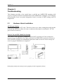
Chapter 5 Troubleshooting ........................................................................................................5-1
5.1 Hardware Quick Installation........................................................................... 5-1
5.2 BIOS Setting ....................................................................................................... 5-3
5.3 FAQ ..................................................................................................................... 5-5
Appendix A
Appendix B
Preface
How to Use This Manual
The manual describes how to configure your WADE-8656 system board to meet
various operating requirements. It is divided into five chapters, with each chapter
addressing a basic concept and operation of Single Host Board.
Chapter 1 : System Overview. Presents what you have in the box and give you an
overview of the product specifications and basic system architecture for this series
model of single host board.
Chapter 2 : Hardware Configuration. Shows the definitions and locations of Jumpers
and Connectors that you can easily configure your system.
Chapter 3 : System Installation. Describes how to properly mount the CPU, main
memory and Compact Flash to get a safe installation and provides a programming
guide of Watch Dog Timer function.
Chapter 4 : BIOS Setup Information. Specifies the meaning of each setup
parameters, how to get advanced BIOS performance and update new BIOS. In
addition, POST checkpoint list will give users some guidelines of trouble-shooting.
Chapter 5 : Troubleshooting. Provides various useful tips to quickly get WADE-8656
running with success. As basic hardware installation has been addressed in Chapter
3, this chapter will basically focus on system integration issues, in terms of backplane
setup, BIOS setting, and OS diagnostics.
The content of this manual is subject to change without prior notice. These changes
will be incorporated in new editions of the document. Portwell may make
supplement or change in the products described in this document at any time.
Updates to this manual, technical clarification, and answers to frequently asked
questions will be shown on the following web site : http://www.portwell.com.tw/.
System Overview
Chapter 1
System Overview
1.1
Introduction
AMDY-7002 series, the embedded motherboard of Mini-ITX form factor. Combine
with either the AMD®Fusion G series-T56N FT1 processor. The AMD Fusion G series
processor is the world’s first integrated circuit to combine a low-power CPU and a
discrete-level GPU into a single die. This graphics integration provides high graphic
& multi-media performance in a small form factor and power efficient platform. CPU
configurations are available with single or dual X86 cores, at 18W TDP (Thermal
Design Power). That makes the system more powerful and reliable with smaller and
quieter cooling fan.
AMD®HD6320, the discrete GPU of T56N FT1 processor is a leading Embedded
Integrated Graphics Processors supports DirectX® 11, OpenGL 4.0 and OpenCL 1.1.
Wide multi-media capability with H/W decode of H.264, VC-1, MPEG2, WMV, DivX
and Adobe Flash delivers greater performance per watt of previous AMD platform.
The graphic memory is shared from system memory (UMA).Offering a stable and
reliable embedded computing platform to users who needs smooth HD& 3D visual
effects experiences.
The AMD Fusion controlling hub A55E not only has rich I/O support of USB& COM,
but also adds new features such as SATA 3.0, RAID (0/1/5/10), Generation 2 PCI
Express, PCI local bus, Gigabit Ethernet MAC, and HD audio. All these features make
AMDY-7002 a value-oriented solution for applications requiring a balance of CPU&
multi-media performance.
To meet expansion cards requirement, the AMDY-7002 series was designed one PCI
Express x1 slot and one PCI slot. By these two slots, AMDY-7002 can support PCI
Express x1 or PCI add-on cards such as ATI graphic card to meet multi-display
function. There is also a Mini-PCI Express (half sized) socket on board to support
special function such as SSD card or wireless module.
AMDY-7002 series features:
z
z
z
z
z
Support AMD®Fusion G series-T56N FT1 processors in BGA package.
Deliver up to 4GB maximum DDR3 1333/1066 on one SO-DIMM socket.
Discrete graphic processor of ATI HD6320 supports DirectX® 11
Support dual display which is chosen from LVDS, VGA and DVI interfaces
(depends on model type).
Support High Definition Audio codec.
AMDY-7002 User’s Manual
1-1
System Overview
z
z
z
z
z
High speed Gigabit Ethernet based on PCI Express x1, high bandwidth I/O
interface.
Five onboard SATA 3.0 ports support IDE/AHCI mode and RAID
function(RAID0,1,5& 10)
Rich I/O connections which included total 14*USB ports and 8*COM ports.
Expansion slot such as PCI-Express x1 slot, PCI slot and half sized Mini
PCI-Express socket.
Adopt CF and CFast sockets as extra storage devices.
AMDY-7002 series Mini-ITX embedded motherboards provide powerful graphic
performance and low power consumption and I/O connections. Makes AMDY-7002
series the best solution for media, digital signage, gaming and POS applications.
1.2
Check List
AMDY-7002 series package should contain the following basic items:
z
z
z
z
One AMDY-7002 series Mini-ITX embedded motherboard
One Installation Resources& User Manual CD
One Rear I/O bracket
SATA signal cable
Optional:
z
z
z
Serial ports cable kit
SATA power cable
PCI Express x1& PCI riser card
If any of these items is damaged or missing, please contact your vendor and keep all
packing materials for future replacement and maintenance.
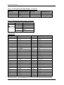
1.3
z
Products Specification
Main Processor
- AMD®Fusion G series-T56N FT1 processor
z BIOS
-Phoenix system BIOS with SPI Serial CMOS EEPROM
z Main Memory
-Support dual channel DDR3 memory interface
-Non-ECC only
-One SO-DIMM sockets support 1333/1066 DDR3 SDRAM up to 4GB system
memory.
z L2 Cache Memory
-Built-in processor
AMDY-7002 User’s Manual
1-2
System Overview
z
Chipset
-AMD®A55E FCH
z Display
- AMD HD-6320 discrete GPU from G-series T56N processor@500MHz Core Freq.
-Up to 2 display choose form VGA, DVI or LVDS interfaces (depends on model type)
z Extension
-PCI-Express x1 slot
-PCI slot
-Half Sized PCIE Mini-Card *1
z Storage
-SATA ports* 5 onboard
-Compact Flash Socket * 1
-CFAST Socket *1
z Ethernet
-Realtek RTL8111DL *2
-Support Boot from LAN (PXE)
-Support Wake on LAN
z Serial Port
-Support 8 UART in total
-COM1,2 support RS232 only.
-COM3,4,5,6 support RS232/422/485 with jumper selection and power .
-COM7,8 support RS232 with power
z USB Interface
- Support 14*USB ports in total
-6*USB on rear panel connectors.
-6*USB on board Pin Header, 2.54mm Pitch
-1 is for internal vertical USB connector
-1 is for internal half size PCIE mini card
z Auxiliary I/O Interface
-System reset switch, external speaker and HDD active LED, etc
z Real Time Clock
-Support Y2K Real Time Clock/Calendar with battery back for 7-years data retention
z Watchdog Timer
-Support WDT function through software programming for enable/disable and
interval setting
-Generate system reset
z Auxiliary I/O Interface
-System reset switch, external speaker and HDD active LED, etc
z High Driving GPIO
-Support 8 programmable high driving GPIO
z Cooling Fan
-System FAN controlled by A55E
z System Monitoring Feature
-Monitor CPU temperature, system temperature and major power sources, etc
z Outline Dimension
-170 mm (L) x 170(W) mm
AMDY-7002 User’s Manual
1-3
System Overview
z Power Requirement
-ATX 20Pin Connector
-ATX 4Pin Connector for 12V input
z
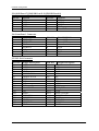
Testing Configuration
CPU Type
AMD G-series T56N Processor 1.6GHz L2:1024K
SBC BIOS
R.1.00.W4 01/11/2011
Memory
Transcend DDR3 1066 2GB*1 (SEC K4B1G0846F)
VGA Card
Onboard AMD Radeon HD 6250 Graphics
VGA Driver
AMD Embedded GPU and Chipset Vista/Win7 Driver version 8.88
LAN Card
Onboard Realtek RTL8111DL PCle GBE Family Controller
LAN Driver
Realtek RTL8111DL Ethernet Controller Driver Ver: 5.754.0308.2010
Audio Card
Onboard Realtek ALC886 High Definition Audio
Audio Driver
Realtek ALC-886 High Definition Audio System Software Ver: R2.49
CHIP Driver
N/A
SATA HDD
Seagate ST3500411SV 500GB
SATA CDROM
LITE-ON LH-20A1S DVD-ROM
Power Supply
FSP350-60GLC
z Operating Temperature
-0 ~ 60℃
z Storage Temperature
-20 ~ 80℃
z Operating Humidity
-Operation Humidity: 5% ~ 95%, non-condensing
AMDY-7002 User’s Manual
1-4
System Overview
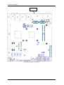
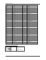
1.3.1
Mechanical Drawing
AMDY-7002 User’s Manual
1-5
System Overview
AMDY-7002 User’s Manual
1-6
System Overview
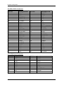
1.4
System Architecture
All of details operating relations are shown in WADE-8656 series System Block
Diagram.
VGA
VGA
24Bit LVDS
2 Channel
24Bit LVDS
2 Channel
LVDS
LVDS
PCIEx1
AMD
G-Series
APU
DP0
CH7511
Single Channel
Horizontal SODIMM
DDR3 1066/1333
DDR3
RTL8111DL
RJ45
Connector
PCIEx1
RTL8111DL
DP1
CH7511
PCIEx1
Compact Flash
Connector
JMB368
DVI-D Conn
DVI
PCIEx1
4-Lane UMI
PCIEx1 Slot *1
Dual RJ45+USB x2
Connector
Single
USB*2
Connector
USB x7
USB x6
Pin Header
CFAST
*1
AMD
ECH
(Embedded
Controller Hub,
FCH)
A55E
(Hudison-E1)
PCI
PCI Slot *1
HDA
ALC886
SPI
BIOS
PCIEx1
ITE IT8728F
(WDT + H/W
Monitor)
LPC Bus
COM1 RS232/RI#
COM2 RS232/RI#
RS232/RS485
ITE
IT8783
COM3 RS232/422/485 w/ Power
COM4 RS232/422/485 w/ Power
COM5 RS232/422/485 w/ Power
COM6 RS232/422/485 w/ Power
COM7 RS232/w Power
COM8 RS232/w Power
8 Bit GPIO
20 Pin ATX
Rear IO
Connectors
Audio
Jack
SATA
x5
USB
Half-sized
Mini Card
Audio
Onboard
Connectors
Switch
12V
VCC
GND
3V
5VSB
AMDY-7002 System Block Diagram
AMDY-7002 User’s Manual
1-7
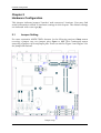
Hardware Configuration
Chapter 2
Hardware Configuration
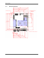
This chapter indicates jumpers’ headers’ and connectors’ locations. User may find
useful information related to hardware settings in this chapter. The default settings
are indicated with a star sign (★)
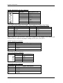
2.1
Jumper Setting
For users customize AMDY-7002’s features. In the following sections, Short means
covering a jumper cap over jumper pins; Open or N/C (Not Connected) means
removing a jumper cap from jumper pins. Users can refer to Figure 1 and Figure 2 for
the Jumper allocations.
Jumper map
AMDY-7002 User’s Manual
2-1
Hardware Configuration
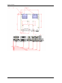
RTL8111D
L
Connector location on top layer
AMDY-7002 User’s Manual
2-2
Hardware Configuration
Connector location on bottom layer
Jumper setting
Reference
JP1
JP2
AMDY-7002 User’s Manual
Description
LVDS0 panel VDD level selector
1-2: +3.3V
5-6: +5V(default)
COM1 (J2 lower) connector pin 9 function selector
1-2: +5V power
3-4: +12V
2-3
Hardware Configuration
JP3
JP4
JP5
JP6
JP7
JP8
JP9
JP10
JP11
JP12
AMDY-7002 User’s Manual
5-6: Ring in (default)
COM2 (J2 upper) connector pin 9 function selector
1-2: +5V power
3-4: +12V
5-6: Ring in (default)
LVDS1 (J8) panel VDD level selector
1-2: +3.3V
5-6: +5V(default)
* Note 1
LVDS0 (J7) panel back light inverter level and polarity
selector:
1-3, 2-4
5V, Active High (default)
1-3, 4-6 12V, Active High
3-5,2-4
5V, Active Low
3-5,4-6
12V, Active Low
LVDS1 (J8) panel back light inverter level and polarity
selector:
1-3, 2-4
5V, Active High (default)
1-3, 4-6 12V, Active High
3-5,2-4
5V, Active Low
3-5,4-6
12V, Active Low
Note 1
COM6 protocol jumper setting:
RS-232: 5-6,9-11,10-12,15-17,16-18 (default)
RS-422: 3-4,7-9,8-10,13-15,14-16,21-22
RS-485: 1-2,7-9,8-10,19-20
CMOS battery charge / discharge selector:
1-2: charge (default)
2-3: discharge
COM5 (J25) protocol jumper setting:
RS-232: 5-6,9-11,10-12,15-17,16-18 (default)
RS-422: 3-4,7-9,8-10,13-15,14-16,21-22
RS-485: 1-2,7-9,8-10,19-20
COM5 connector (J25) pin 8 function selector
1-2: +5V power
3-4: +12V
5-6: Ring in (default)
COM6 connector (J26) pin 8 function selector
1-2: +5V power
3-4: +12V
5-6: Ring in (default)
COM3 connector (J31) pin 8 function selector
1-2: +5V power
3-4: +12V
5-6: Ring in (default)
2-4
Hardware Configuration
JP13
SW1
COM4 connector (J32) pin 8 function selector
1-2: +5V power
3-4: +12V
5-6: Ring in (default)
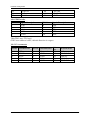
LVDS0 (J7) panel type selector. 0=Switch ON; 1= Switch
OFF
Panel
model
SW1[3..0] name
Resolution
1024x768x18bit, single
AUO G150XG01 channel
0000
0001
圖示標示為 0000
Default Setting 0011
應為下圖
Reserved
G121SN01 V3
0010
0011(defaul
G170EG01
t)
0100
M240HW01
Reserved
800x600x24bit, single
channel
1280x1024x24bit,
dual channel
1920x1080x24bit, dual
channel
0101~1111 Reserved
Reserved
Note: SW1: 0001 panels has not been validate yet.
SW2
圖示標示為 0000
Default Setting 0011
應為下圖
LVDS1 (J8) panel type selector. 0=Switch ON; 1= Switch
OFF
Panel
model
SW1[3..0] name
Resolution
1024x768x18bit,
AUO G150XG01 Single channel
0000
0001
Reserved
G121SN01 V3
0010
0011(defaul
G170EG01
t)
0100
M240HW01
Reserved
800x600x24bit,
single channel
1280x1024x24bit,
dual channel
1920x1080x24bit,
dual channel
0101~1111 Reserved
Reserved
Note: SW1: 0001 panels has not been validate yet.
* Note 1: LVDS1 is an optional function.
AMDY-7002 User’s Manual
2-5
Hardware Configuration
Connector function description:
Reference Function description
J1
DVI-D connector
J2
COM1 (lower) + COM2 (upper) connector
J3
Audio connector. MIC (pink), line out(lime), line in(light blue)
J4
PS2 connector + USB port 0, 1 connector
J5
LAN2 + USB port 2, USB port 3 connector
J6
LAN1 + USB port 4, USB port 5 connector
J7
LVDS0 connector
J8
LVDS1 connector.
Note 1
J9
LVDS0 back light adjustment connector.
J10
LVDS0 back light inverter module connector
J11
LVDS1 back light adjustment connector
J12
LVDS1 back light inverter module connector
J13
DDR3 SO-DIMM
J14
Standard PCI slot
J15
CPU fan connector
J16
Mini PCI-Express connector
J17
ATX power connector
J18
SATA 0
J19
SATA 1
J20
SATA 2
J21
SATA 3
J22
COM7
J23
COM8
J24
System fan connector
J25
COM5
J26
COM6
J27
SATA5
J28
PC Speaker connector
J29
SATA device power (for J27)
J30
USB port 10
J31
COM3
J32
COM4
J33
USB port 6, 7
J34
USB port 12, 13
J35
USB port 8, 9
J36
Front panel connector
J37
PCI-E slot
J38
CFAST socket
J39
CF socket
J40
GPIO Header
J41
VGA Connector
AMDY-7002 User’s Manual
2-6
Hardware Configuration
Pin Assignments of Connectors
J1: VGA Connector
PIN NO. DESCRIPTION
1
2
3
4
5
6
7
8
PIN NO.
DVI D2DVI D2+
GND
NC
NC
DVI DDC CLK
DVI
DDC
DATA
NC
DESCRIPTION
PIN NO. DESCRIPTION
9
10
11
12
13
14
15
DVI D1DVI D1+
GND
NC
NC
+5V (350mA)
GND
17
18
19
20
21
22
23
DVI D0DVI D0+
GND
NC
NC
GND
CLK+
16
Hot plug
24
CLK-
J2: COM1, COM2 connector
PIN No. Signal Description
PIN No. Signal Description
1
DCD#
6
DSR#
2
RXD
7
RTS#
3
TXD
8
CTS#
4
DTR#
9
RI
5
GND
10
*Note: Upper connector is COM2; lower connector is COM1
J3: Audio Connector
PIN No.
1 (Blue)
2 (Lime)
3 (Pink)
Description
Line In
Line Out
Micro phone
J4: PS2 + dual USB port Connector
USB PIN No.
1
2
3
4
PS2 PIN No.
1
2
3
4
5
6
Signal Description
USB Power(5V)
USB DATAUSB DATA+
USB GND
Signal Description
MDAT
KDAT
GND
Power
MCLK
KCLK
AMDY-7002 User’s Manual
2-7
Hardware Configuration
J5.J6 USB port 1,2,3,4 and LAN1, LAN2 RJ-45 Connector
USB PIN No.
Signal Description
USB Power(5V)
USB DATAUSB DATA+
USB GND
RJ-45 PIN No.
Signal Description
1
MDIA+
2
MDIAMDIB+
3
4
MDIC+
5
MDIC6
MDIB7
MDID+
8
MDID*Note: For J5, upper USB port is port 3, lower port is port 4. For J6, upper USB
port is port 1 and lower USB port is port 2.
1
2
3
4
J7 :LVDS(LVDS0) and J8(LVDS1) Connector
AMDY-7002 User’s Manual
PIN
NO.
DESCRIPTION
PIN
NO.
DESCRIPTION
2
4
6
8
10
12
14
16
18
20
22
24
26
28
30
Panel VDD
CHA TX0CHA TX1CHA TX2CHA TX3CHA CLKDDC DATA
GND
CHB TX0CHB TX1CHB TX2CHB TX3CHB CLKNC
GND
1
3
4
5
7
11
13
15
17
19
21
23
25
27
29
Panel VDD
CHA TX0+
CHA TX1+
CHA TX2+
CHA TX3+
CHA CLK+
DDC CLK
GND
CHB TX0+
CHB TX1+
CHB TX2+
CHB TX3+
CHB CLK+
NC
GND
2-8
Hardware Configuration
J9, J11 : LVDS panel back light dimmer Connector
PIN NO.
DESCRIPTION PIN NO.
1
GND
2
3
NC
4
5
GND
6
*Note: J9 is dedicate to LVDS0; J11 is dedicate to LVDS1
DESCRIPTION
Back Light Up
NC
Back Light Down
J10, J12: LVDS back light inverter Connector
PIN NO.
1
2
3
4
5
DESCRIPTION
Enable
GND
+12V
GND
+5V
J14: PCI Slot
PIN No.
B1
B2
B3
B4
B5
B6
B7
B8
B9
B10
B11
B12
B13
B14
B15
B16
B17
B18
B19
B20
B21
B22
B23
B24
B25
B26
Function
-12V
TCK
GND
NC
+5V
+5V
PIRQB#
PIRQD#
NC
NC
NC
GND
GND
NC
GND
PCI 33MHz CLK
GND
PCI REQ#
+5V
AD31
AD29
GND
AD27
AD25
+3.3V
C/BE3#
AMDY-7002 User’s Manual
PIN No.
A1
A2
A3
A4
A5
A6
A7
A8
A9
A10
A11
A12
A13
A14
A15
A16
A17
A18
A19
A20
A21
A22
A23
A24
A25
A26
Function
TRST#
+12V
PTMS
PTDI
+5V
PIRQA#
PIRQC#
+5V
NC
+5V
NC
GND
GND
+3.3VSB
RESET#
+5V
PGNT#
GND
PCI PME#
AD30
+3.3V
AD28
AD26
GND
AD24
IDSEL (AD21)
2-9
Hardware Configuration
B27
B28
B29
B30
B31
B32
B33
B34
B35
B36
B37
B38
B39
B40
B41
B42
B43
B44
B45
B46
B47
B48
B49
B50
B51
B52
B53
B54
B55
B56
B57
B58
B59
B60
B61
B62
AD23
GND
AD21
AD19
+3.3V
AD17
C/BE2#
GND
IRDY#
+3.3V
DEVSEL#
GND
PLOCK#
PERR#
+3.3V
SERR#
+3.3V
C/BE1#
AD14
GND
AD12
AD10
GND
KEY
KEY
AD8
AD7
+3.3V
AD5
AD3
GND
AD1
+5V
ACK64#
+5V
+5V
A27
A28
A29
A30
A31
A32
A33
A34
A35
A36
A37
A38
A39
A40
A41
A42
A43
A44
A45
A46
A47
A48
A49
A50
A51
A52
A53
A54
A55
A56
A57
A58
A59
A60
A61
A62
+3.3V
AD22
AD20
GND
AD18
AD16
+3.3V
FRAME#
GND
TRDY#
GND
STOP#
+3.3V
SMB CLK
SMB DATA
GND
PAR
AD15
+3.3V
AD13
AD11
GND
AD9
KEY
KEY
C/BE0#
+3.3V
AD6
AD4
GND
AD2
AD0
+5V
REQ64#
+5V
+5V
J15: CPU Fan, J24: System Fan
PIN NO.
1
2
3
AMDY-7002 User’s Manual
DESCRIPTION
GND
Power Input
Pulse
2-10
Hardware Configuration
J16: Mini PCI-E Connector
PIN NO.
1
3
5
7
9
11
13
15
17
19
21
23
25
27
29
31
33
35
37
39
41
43
45
47
49
51
DESCRIPTION
WAKE#
NC
NC
CLKREQ#
GND
CLOCKCLOCK+
GND
NC
NC
GND
PCI-E RXPCI-E RX+
GND
GND
PCI-E TXPCI-E TX+
GND
GND
+3.3VSB
+3.3VSB
GND
NC
NC
NC
NC
PIN NO.
2
4
6
8
10
12
14
16
18
20
22
24
26
28
30
32
34
36
38
40
42
44
46
48
50
52
DESCRIPTION
+3.3VSB
GND
+1.5V
NC
NC
NC
NC
NC
GND
PU to +3.3VSB
RESET#
+3.3VSB
GND
+1.5V
SMB CLK
SMB DATA
GND
USBDUSBD+
GND
NC
NC
NC
+1.5V
GND
+3.3VSB
J17: ATX Power Connector
PIN No.
11
12
13
14
15
16
17
18
19
20
Function
+3.3V
-12V
GND
PSON#
GND
GND
GND
NC
+5V
+5V
AMDY-7002 User’s Manual
PIN No.
1
2
3
4
5
6
7
8
9
10
Function
+3.3V
+3.3V
GND
+5V
GND
+5V
GND
POWER OK
+5VSB
+12V
2-11
Hardware Configuration
J18.J19, J20 ,J21,J27: SATA Connector
PIN NO.
1
2
3
4
5
6
7
DESCRIPTION
GND
TX+
TXGND
RXRX+
GND
J22 (COM7), J23(COM8), J25(COM5), J26(COM6),J31(COM3),J32(COM4)
PIN No. Function
PIN No.
Function
1
DCD#
2
RXD
3
TXD
4
DTR#
5
GND
6
DSR#
7
RTS#
8
CTS#
9
Power / RI#
10
NC
Note: Function of pin 9 Power / RI# can be define as +5V output, +12V output and
Modem Ring In, depend on jumper setting of JP10, JP11, JP12, JP13.
J28: PC Speaker Connector
PIN No.
1
2
3
4
Signal Description
PC Speaker
NC
GND
+5V
J29: SATA power Connector
PIN NO.
1
2
3
4
DESCRIPTION
+12V
GND
GND
+5V
J30: USB Port 10 Connector
PIN No.
1
2
3
4
Signal Description
USBV
USBDUSBD+
USBG
AMDY-7002 User’s Manual
2-12
Hardware Configuration
J33: (USB Port 6.7),J34(USB Port 12.13,J35(USB Port 8.9)
PIN No.
1
3
5
7
Function
+5V
USBDAUSBDA+
GND
PIN No.
2
4
6
8
10
Function
+5V
USBDBUSBDB+
GND
Case GND
J36: Front Panel Connector
PIN NO.
1
3
5
7
9
11
13
DESCRIPTION
HDD LED+
HDD LEDGND
SYSRST#
NC
GND
Reserved
PIN NO.
2
4
6
8
10
12
14
DESCRIPTION
Power LED+
Power LEDPower button#
GND
NC
GND
NC
J37: PCI-Ex1 Connector
PIN NO.
B1
B2
B3
B4
B5
B6
B7
B8
B9
B10
B11
B12
B13
B14
B15
B16
B17
B18
Single Description
+12V
+12V
+12V
GND
SMBUS CLK
SMBUS DATA
GND
3.3V
NC
3.3V standby
WAKE UP#
NC
GND
PCIE_TX0+
PCIE_TX0GND
PRESENT#
GND
AMDY-7002 User’s Manual
PIN NO. Single Description
A1
NC
A2
+12V
A3
+12V
A4
GND
A5
NC
A6
NC
A7
NC
A8
NC
A9
+3.3V
A10
+3.3V
A11
PCIE_RST#
A12
GND
A13
PCIE_CLOCK+
A14
PCIE_CLOCKA15
GND
A16
PCIE_RX0+
A17
PCIE_RX0A18
GND
2-13
Hardware Configuration
J38: CFAST connector
PIN NO.
S1
S2
S3
S4
S5
S6
S7
Single Description
GND
SATA TX+
SATA TXGDN
SATA RXSATA RX+
GND
PIN NO.
PC1
PC2
PC3
PC4
PC5
PC6
PC7
PC8
PC9
PC10
PC11
PC12
PC13
PC14
PC15
PC16
PC17
Single Description
NC
GND
NC
NC
NC
NC
GND
Link to LED D45
Link to LED D45
NC
NC
NC
+3.3V
+3.3V
GND
GND
NC
J39: CF card socket
PIN NO.
1
2
3
4
5
6
7
8
9
10
11
12
13
14
15
16
17
18
19
20
21
22
DESCRIPTION
GND
DATA3
DATA4
DATA5
DATA6
DATA7
CS#0
GND
GND
GND
GND
GND
+3.3V
GND
GND
GND
GND
A2
A1
A0
DATA0
DATA1
AMDY-7002 User’s Manual
PIN NO.
26
27
28
29
30
31
32
33
34
35
36
37
38
39
40
41
42
43
44
45
46
47
DESCRIPTION
Pull down
DATA11
DATA12
DATA13
DATA14
DATA15
CS#1
Pull down
IOR#
IOW#
Pull up
IRQ
+3.3V
Pull up
NC
RESET#
IORDY
DREQ
DACK
ACT#
Pull down
DATA8
2-14
Hardware Configuration
23
24
25
DATA2
NC
Pull down
48
49
50
DATA9
DATA10
GND
J40: GPIO header
PIN No.
Signal Description
PIN No.
Signal Description
1
GP0
2
GP4
3
GP1
4
GP5
GP2
5
6
GP6
7
GP3
8
GP7
9
GND
10
VCC
*Note:
This GPIO uses TTL level.
GPIO base address is 4EE, default direction is output.
J41: VGA connector
PIN NO. DESCRIPTION
1
2
3
4
5
RED
GREEN
BLUE
NC
GND
AMDY-7002 User’s Manual
PIN NO. DESCRIPTION
6
7
8
9
10
Reserved
GND
GND
NC
GND
PIN
NO.
DESCRIPTION
11
12
13
14
15
NC
DDC DATA
HSYNC
VSYNC
DDC CLK
2-15
System Installation
Chapter 3
System Installation
This chapter provides you with instructions to set up your system. The additional
information is enclosed to help you set up onboard PCI device and handle Watch Dog
Timer (WDT) and operation of GPIO in software programming.
3.1
AMD G-Series FT1 Processors
The AMDY-7002 supports AMD G-Series FT1 (FCBGA-413) CPU. It provides very
low TDP for different applications that need fan-less. It is using latest AMD G-Series
Processor. Please see attached table for more detail.
The core logic chipset is AMD A55E ECH. From 2011, this 2-chips new platform
will be main-stream for next generation AMD platform architecture.
All the AMD FT1 CPU and ECH chipset are in AMD embedded roadmap that has
longevity support at least 2016.
AMDY-7002-T56N
AMDY-7002-T56ND
3.2
․1.6GHz, Dual Core, Dual LAN with CFAST and
Express mini-card socket, 8 COM, single DP to LVDS
(DP0), with DVI
․1.6GHz, Dual Core, Dual LAN with CFAST and Express
mini-card socket, 8 COM , with dual
DP to LVDS, NO DVI
Main Memory
AMDY-7002 provide 1 x 204-pin SO-DIMM sockets which supports 1066/1333
DDR3-SDRAM as main memory, Non-ECC (Error Checking and Correcting),
non-register functions. The maximum memory size can be up to 4GB capacity.
Memory clock and related settings can be detected by BIOS via SPD interface.
For system compatibility and stability, do not use memory module without brand.
Memory configuration can be either one double-sided DIMM in either one DIMM
socket or two single-sided SO-DIMM in both sockets.
Watch out the contact and lock integrity of memory module with socket, it will
impact on the system reliability. Follow normal procedures to install memory module
into memory socket. Before locking, make sure that all modules have been fully
inserted into the card slots.
AMDY-7002 User’s Manual
3-1
System Installation
3.3
Installing the Single Board Computer
To install your AMDY-7002 into standard chassis or proprietary environment, please
perform the following:
Step 1 : Check all jumpers setting on proper position
Step 2 : Install and configure CPU and memory module on right position
Step 3 : Place AMDY-7002 into the dedicated position in the system
Step 4 : Attach cables to existing peripheral devices and secure it
WARNING
Please ensure that SBC is properly inserted and fixed by mechanism.
Note:
Please refer to section 3.3.1 to 3.3.4 to install INF/VGA/LAN/Audio drivers.
3.3.1
Chipset Component Driver
The chipset on AMDY-7002 is a new chipset that a few old operating systems might
not be able to recognize. To overcome this compatibility issue, for Windows
Operating Systems such as Windows XP /WIN7, please install its INF before any of
other Drivers are installed. You can find very easily this chipset component driver in
AMDY-7002 CD-title.
3.3.2
Integrated Graphics
AMDY-7002 has APU integrated next generation HD6320 DX11 discrete GPU. The
graphic memory is shared from system memory (UMA), max is TBD.
Drivers Support
Please find driver in the AMDY-7002 CD-title. Drivers support Windows XP,
Windows 7.
3.3.3
Realtek Gigabit Ethernet Controller
Drivers Support
Two Gigabit Ethernet controllers are supported on AMDY-7002 Series. Both Ethernet
need to be PCIEx1 interface and support above functionality:
z PXE, Boot from LAN, can be disabled by BIOS individually.
z WOL, Wake on LAN, can be disabled by BIOS individually.
z Support 10/100/1000 access.
z Link / Access LED (Green), Speed LED (Black-10, Green-100, Orange-1000). If
LAN cable not installed, all LED need to be turn off.
AMDY-7002 User’s Manual
3-2
System Installation
Please find Realtek RTL8111DL LAN driver in /Ethernet directory of AMDY-7002
CD-title. The drivers support Windows XP /7.
LED Indicator (for LAN status)
AMDY-7002 provides two LED indicators to report Realtek RTL8111DL Gigabit
Ethernet interface status. Please refer to the table below as a quick reference guide.
8111C
Color
Name of LED
Status
LED
Orange
Speed
LED
3.3.4
Orange
Operation of Ethernet Port
Linked
Active
LAN Linked & Active LED
On
Blinking
LAN speed LED
Giga
Mbps
Orange
Green
100 Mbps 10 Mbps
Green
Off
Audio Controller
Please find Realtek ALC886 Audio driver form AMDY-7002 CD-title. The drivers
support Windows XP /7.
3.4
Clear CMOS Operation
The following table indicates how to enable/disable Clear CMOS Function hardware
circuit by putting jumpers at proper position.
3
2
1
Charge
3
2
1
Discharge
I
T
AMDY-7002 User’s Manual
3-3
System Installation
3.5
WDT Function
The working algorithm of the WDT function can be simply described as a counting
process. The Time-Out Interval can be set through software programming. The
availability of the time-out interval settings by software or hardware varies from
Boards to boards.
WDT Control Command Example
#include <stdio.h>
#include <conio.h>
#include <dos.h>
#define SIO_Port 0x2E
#define SIO_Port2 0x4E
#define GPIO_LDN 0x07
void Enter_IT872x_SIO() {
outportb(SIO_Port, 0x87);
outportb(SIO_Port, 0x01);
outportb(SIO_Port, 0x55);
outportb(SIO_Port, 0x55);
}
void Set_LDN(unsigned char LDN) {
outportb(SIO_Port, 0x07);
outportb(SIO_Port+1, LDN);
printf("LDN=%x\n", LDN);
}
void Set_Register(unsigned char offset, unsigned char value) {
outportb(SIO_Port, offset);
outportb(SIO_Port+1, value);
printf("Write offset:%x = %x\n", offset, value);
}
int main(void) {
printf("test string\n");
Enter_IT872x_SIO();
Set_LDN(GPIO_LDN);
Set_Register(0x72, 0xC0);
Set_Register(0x73, 0x05);
printf("System will reset in 5 seconds\n");
return 0;
}
AMDY-7002 User’s Manual
3-4
System Installation
3.6
GPIO
The AMDY-7002 provides 8 programmable input or output ports that can be
individually configured to perform a simple basic I/O function. Users can configure
each individual port to become an input or output port by programming register bit
of I/O Selection. To invert port value, the setting of Inversion Register has to be
made.
Port values can be set to read or write through Data Register.
3.6.1
Pin assignment
JP11
Function
Pin 1
GP 0
Pin 2
GP 4
Pin 3
GP 1
Pin 4
GP 5
Pin 5
GP 2
Pin 6
GP 6
Pin 7
GP 3
Pin 8
GP 7
Pin 9
GND
Pin 10
VCC
*Note:
a. This GPIO uses TTL level.
b. GPIO base address is 4EE, default direction is output.
3.6.2
Demo Program
The following is demo program source code by C language.
#include <stdio.h>
#include <conio.h>
#include <stdlib.h>
#define SIO_Port 0x2E
#define SIO_Port2 0x4E
#define GPIO_LDN 0x07
#define GPIO_Base 0x0A00
//Enter SIO
void Enter_IT872x_SIO() {
outp(SIO_Port, 0x87);
outp(SIO_Port, 0x01);
outp(SIO_Port, 0x55);
outp(SIO_Port, 0x55);
}
//Select LDN
AMDY-7002 User’s Manual
3-5
System Installation
void Set_LDN(unsigned char LDN) {
outp(SIO_Port, 0x07);
outp(SIO_Port+1, LDN);
//printf("LDN=%x\n", LDN);
}
//Set register offset to Value
void Set_Register(unsigned char offset, unsigned char value) {
outp(SIO_Port, offset);
outp(SIO_Port+1, value);
//printf("Write offset:%x = %x\n", offset, value);
}
//Or register
void Or_Register(unsigned char offset, unsigned char value) {
outp(SIO_Port, offset);
outp(SIO_Port+1, inp(SIO_Port+1) | value);
//printf("Write offset:%x = %x\n", offset, value);
}
//And register
void And_Register(unsigned char offset, unsigned char value) {
outp(SIO_Port, offset);
outp(SIO_Port+1, inp(SIO_Port+1) & value);
//printf("Write offset:%x = %x\n", offset, value);
}
int main(void) {
int result;
printf("RUBY-D712 GPIO Test:\n");
//pin1 =11
//pin3 =12
//pin5 =47
//pin7 =50
//pin9 =74
//pin11=75
//pin13=76
//pin15=77
//pin2 =14
//pin4 =35
//pin6 =36
//pin8 =37
//pin10=70
//pin12=71
//pin14=72
//pin16=73
Enter_IT872x_SIO();
Set_LDN(GPIO_LDN);
//Enable GPIO
//Or_Register(0xC0,0x46) //11,12,14
AMDY-7002 User’s Manual
3-6
System Installation
//Or_Register(0xC2,0xE0) //35,36,37
//Or_Register(0xC3,0x80) //47
//Or_Register(0xC4,0x01) //50
//Set Output
Or_Register(0xC8,0x06); //11,12
Or_Register(0xCB,0x80); //47
Or_Register(0xCC,0x01); //50
Or_Register(0xCE,0xF0); //74,75,76,77
//Set Input
And_Register(0xC8,0xEF); //14
And_Register(0xCA,0x1F); //35,36,37
And_Register(0xCE,0xF0); //70,71,72,73
//output high
outp(GPIO_Base+0,0x06); //11,12
outp(GPIO_Base+3,0x80); //47
outp(GPIO_Base+4,0x01); //50
outp(GPIO_Base+6,0xF0); //74,75,76,77
result=1;
if ((inp(GPIO_Base+0)&0x10)!=0x10) result=0;
if ((inp(GPIO_Base+2)&0xE0)!=0xE0) result=0;
if ((inp(GPIO_Base+6)&0x0F)!=0x0F) result=0;
if (result==0){
printf("Test fail!!\n");
return 1;
}
//output low
outp(GPIO_Base+0,inp(GPIO_Base+0)&0xF9); //11,12
outp(GPIO_Base+3,inp(GPIO_Base+3)&0x7F); //47
outp(GPIO_Base+4,inp(GPIO_Base+4)&0xFE); //50
outp(GPIO_Base+6,inp(GPIO_Base+6)&0x0F); //74,75,76,77
result=1;
if ((inp(GPIO_Base+0)&0x10)!=0x00) result=0;
if ((inp(GPIO_Base+2)&0xE0)!=0x00) result=0;
if ((inp(GPIO_Base+6)&0x0F)!=0x00) result=0;
if (result==0){
printf("Test fail!!\n");
return 1;
}
///////////////////////////////////////////////////
//Set Input
And_Register(0xC8,0xF9); //11,12
And_Register(0xCB,0x7F); //47
And_Register(0xCC,0xFE); //50
And_Register(0xCE,0x0F); //74,75,76,77
//Set output
Or_Register(0xC8,0x10); //14
AMDY-7002 User’s Manual
3-7
System Installation
Or_Register(0xCA,0xE0); //35,36,37
Or_Register(0xCE,0x0F); //70,71,72,73
//output high
outp(GPIO_Base+0,0x10); //14
outp(GPIO_Base+2,0xE0); //35,36,37
outp(GPIO_Base+6,0x0F); //70,71,72,73
result=1;
if ((inp(GPIO_Base+0)&0x06)!=0x06) result=0; //11,12
if ((inp(GPIO_Base+3)&0x80)!=0x80) result=0; //47
if ((inp(GPIO_Base+4)&0x01)!=0x01) result=0; //50
if ((inp(GPIO_Base+6)&0xF0)!=0xF0) result=0; //74,75,76,77
if (result==0){
printf("Test fail!!\n");
BIOS Setup Information
WADE-8011/WADE-8012 User’s Manual 3-13
return 1;
}
//output low
outp(GPIO_Base+0,inp(GPIO_Base+0)&0xEF); //14
outp(GPIO_Base+2,inp(GPIO_Base+2)&0x1F); //35,36,37
outp(GPIO_Base+6,inp(GPIO_Base+6)&0xF0); //70,71,72,73
result=1;
if ((inp(GPIO_Base+0)&0x06)!=0x00) result=0; //11,12
if ((inp(GPIO_Base+3)&0x80)!=0x00) result=0; //47
if ((inp(GPIO_Base+4)&0x01)!=0x00) result=0; //50
if ((inp(GPIO_Base+6)&0xF0)!=0x00) result=0; //74,75,76,77
if (result==0){
printf("Test fail!!\n");
return 1;
}
//getchar ();
printf("Test Pass!!\n");
return 1;
AMDY-7002 User’s Manual
3-8
BIOS Setup Information
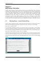
Chapter 4
BIOS Setup Information
AMDY-7002 is equipped with the Phoenix BIOS stored in Flash ROM. These BIOS has
a built-in Setup program that allows users to modify the basic system configuration
easily. This type of information is stored in CMOS RAM so that it is retained during
power-off periods. When system is turned on, AMDY-7002 communicates with
peripheral devices and checks its hardware resources against the configuration
information stored in the CMOS memory. If any error is detected, or the CMOS
parameters need to be initially defined, the diagnostic program will prompt the user
to enter the SETUP program. Some errors are significant enough to abort the start up.
4.1
Entering Setup -- Launch System Setup
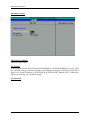
Power on the computer and the system will start POST (Power On Self Test) process.
When the message below appears on the screen, press <F2> key to enter Setup.
Press <F2> to enter SETUP
If the message disappears before you respond and you still wish to enter Setup,
restart the system by turning it OFF and On or pressing the RESET button. You may
also restart the system by simultaneously pressing <Ctrl>, <Alt>, and <Delete> keys.
Press <F2> to Run SETUP or Press <F1> to Comtinue
The BIOS setup program provides a General Help screen. You can call up this screen
from any menu by simply pressing <F1>. The Help screen lists the appropriate keys
to use and the possible selections for the highlighted item. Press <Esc> to exit the Help
screen.
AMDY-7002 User’s Manual
4-1
BIOS Setup Information
4.2
Main Menu
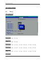
Use this menu for basic system configurations, such as time, date etc.
System Date
The date format is <Day>, <Month> <Date> <Year>. Use [+] or [-] to configure
system Date.
System Time
The time format is <Hour> <Minute> <Second>. Use [+] or [-] to configure system
Time.
AMDY-7002 User’s Manual
4-2
BIOS Setup Information
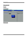
System information
Display system information.
Display system information.
Boot Feature
Select Boot features
AMDY-7002 User’s Manual
4-3
BIOS Setup Information
NumLock
Select Power-on state for NumLock
Error Manager
Display Error Manager Log information.
AMDY-7002 User’s Manual
4-4
BIOS Setup Information
View Error Manager Log
Display Error Manager Log information.
Clear Error Manager Log
Clear Error Manager Log.
AMDY-7002 User’s Manual
4-5
BIOS Setup Information
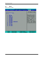
4.3
Advanced
Use this menu to set up the items of special enhanced features.
Select Language
Select Language
Boot Configuration
Set Boot Configuration
AMDY-7002 User’s Manual
4-6
BIOS Setup Information
Quick Boot
Enable/Disable quick boot.
VESA Mode
Enable/Disable VESA mode.
Diagnostic Splash Screen
If you select “Enabled” the diagnostic splash screen always displays during boot.
If you select “Disabled” the diagnostic splash screen does not display unless you
press HOTKEY during boot.
Diagnostic Summary Screen
Display the Diagnostic summary screen during boot.
UEFI Boot
Enable the UEFI boot.
Legacy Boot
Enable the Legacy boot.
Boot Priority
Select priority of boot option between UEFI and Legacy.
BIOS Level USB
Enable/Disable all BIOS support for USB in order to reduce boot time.
USB Legacy Support
Enable/Disable USB BIOS SMM support for mouse, keyboard, mass storage, etc, in
legacy operating systems such as DOS.
AMDY-7002 User’s Manual
4-7
BIOS Setup Information
SMBIOS Event Log
SMBIOS Event Log.
Event Log
Enable/Disable Event Log.
View SMBIOS event Log
View SMBIOS event Log.
Mark SMBIOS events as read
Yes or No
Clean SMBIOS events
Clean SMBIOS events.
AMDY-7002 User’s Manual
4-8
BIOS Setup Information
4.4
AMD
Use this menu to set up the items of special enhanced features.
Platform
Platform BIOS Specification.
AMDY-7002 User’s Manual
4-9
BIOS Setup Information
External USB Host Controller
Enable or disable the external USB hardware.
External Network Controller
Enable or disable the external Network Controller.
External Network Boot ROM
Enable or disable the external LAN Boot ROM.
Display mode
Display mode select.
Universial Console Redirection
Universial Console Redirection.
Processor Options
Processor Options
Processor Core Control
Processor Core Control
AMDY-7002 User’s Manual
4-10
BIOS Setup Information
Thermal Control
Thermal Control
ThermalTrip Enable
ThermalTrip Enable.
TC Enable
In Auto mode, check F3x1F0[19] SerialNumRdDis, if SerialNumRdDis is set to 1, HTC
use AGESA setting. Otherwise check serial number in register F3x1F4 and F3x1F8. If
there is no Serial Number in [D18F3x1F4] & [D18F3x1F4], disable HTC. Otherwise,
CBS does nothing, use AGESA setting.
TC Override
TC Override.
AMDY-7002 User’s Manual
4-11
BIOS Setup Information
CPU Control
CPU Control
General Processor Control
General Processor Control
Target P-State
Target P-State
Auto、Highest、State 0 ~ State 7
AMDY-7002 User’s Manual
4-12
BIOS Setup Information
CIMX SouthBridge
CIMX SouthBridge.
SB GPP OPTION
Enable/Disable
Azalia Device
Azalia Device
Audio OPTION
Azalia OPTION.
USB Devices
USB Devices.
USB Port 0 - 4
Select disable or enable USB1 HCs (Bus 0 Dev 18 Fn 0/2)
USB Port 5 - 9
Select disable or enable USB2 HCs (Bus 0 Dev 19 Fn 0/2)
USB Port 10 - 13
Select disable or enable USB3 HCs (Bus 0 Dev 22 Fn 0/2)
AMDY-7002 User’s Manual
4-13
BIOS Setup Information
SATA Device
SATA Device.
SATA Controller
SATA Controller.
SATA Mode
SATA Mode.
NATICE IDE、RAID、AHCI、LEGACY IDE
ONCHIP IDE OPTION
ONCHIP_IDE OPTION
LEGACY IDE、NATIVE IDE
GEC OPTION
GEC OPTION
AMDY-7002 User’s Manual
4-14
BIOS Setup Information
GEC CONFIG OPTION
GEC_CONFIG OPTION
4.5
Others
SIO Configuration
Sio Configuration
Serial Port 1
Disable、3F8/IRQ5、2F8/IRQ6
Serial Port 2
Disable、3F8/IRQ5、2F8/IRQ6
Serial Port 3
Disable、220/IRQ4、228/IRQ3、238/IRQ4、2E8/IRQ3、338/IRQ4、3E8/IRQ3
Serial Port 4
Disable、220/IRQ4、228/IRQ3、238/IRQ4、2E8/IRQ3、338/IRQ4、3E8/IRQ3
Serial Port 5
Disable、220/IRQ4、228/IRQ3、238/IRQ4、2E8/IRQ3、338/IRQ4、3E8/IRQ3
Serial Port 8
AMDY-7002 User’s Manual
4-15
BIOS Setup Information
Disable、220/IRQ4、228/IRQ3、238/IRQ4、2E8/IRQ3、338/IRQ4、3E8/IRQ3
AMDY-7002 User’s Manual
4-16
BIOS Setup Information
Watch Dog Timer Select
Disable、15 secs、30 secs、1 min、2 mins、3 mins
Power Control
Former State、Always On、Always Off
Hardware Monitor
Hardware Monitor
Wake on Lan and Ring
Wake on Lan and Ring
AMDY-7002 User’s Manual
4-17
BIOS Setup Information
Option on Lan and ring
Disable、Enable
Wake PCIe
Disable、Enable
Power Management
Power Management Configuration
Resume by Alarm
Disable、Enable
AMDY-7002 User’s Manual
4-18
BIOS Setup Information
4.6
Security
Use this menu to set supervisor and user passwords.
Set Supervisor Password
Set or clear the Supervisor account’s password.
Supervisor Hint String
Press Enter to type Supervisor Hint String.
Min. password length
Set the minimum number of characters for password (1-20).
HDD Password Select
Supports user only or both user and master password.
Ser HDD04 User Password
Set HDD04 User Password.
AMDY-7002 User’s Manual
4-19
BIOS Setup Information
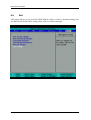
4.7
Boot
Boot Priority Order
AMDY-7002 User’s Manual
4-20
BIOS Setup Information
4.8
Exit
This menu allows you to load the BIOS default values or factory default settings into
the BIOS and exit the BIOS setup utility with or without changes.
AMDY-7002 User’s Manual
4-21
BIOS Setup Information
Exit Saving Changes
Equal to F10, same all changes of all menus, then exit setup configure driver. Finally
resets the system automatically.
Exit Discarding Changes
Equal to ESC, never save changes, then exit setup configure driver.
Load Setup Defaults
Equal to F9. Load standard default values.
Load Optimal Defaults
Load settings for optimized boot time and system performance.
Discard Changes
Load the original value of this boot time. Not the default Setup value.
Save Changes
Save all changes of all menus, but do not reset system
AMDY-7002 User’s Manual
4-22
Appendix B
Chapter 5
Troubleshooting
This chapter provides a few useful tips to quickly get AMDY-7002 running with
success. As basic hardware installation has been addressed in Chapter 2, this chapter
will primarily focus on system integration issues, in terms of BIOS setting, and OS
diagnostics.
5.1
Hardware Quick Installation
ATX Power Setting
AMDY-7002 supports ATX only. Therefore, there is no other setting that really needs
to be set up. However, there are only a connector that must be connected—J17 (20
pins Power Connector) .
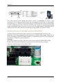
Serial ATA and IDE Hard Disk Setting
The AMDY-7002 supports 5 standard vertical SATA connectors. Each connectors
need to accept standard SATA Cable with lock for HDD/SSD connection. However
SATA DOM is popular for embedded application and we need to reserve keep out
zone for proper installation is required.
AMDY-7002 User’s Manual
5-1
Appendix B
For some special SATA DOM, the power source is embedded in SATA 7 pin
connector. Pin 7 is been re-defined as 5V for this special SATA DOM. On this model,
the 4 (Port [0, 1, 2, and 3]) Vertical SATA Ports for DOM need to have resistors close
to SATA connector pin 7 as a selection of GND or 5V. However, prevent from wrong
usage, the default of those resistors needs to be GND, and design a SMD RED LED to
indicate the Pin7 status prevent from wrong setting. (RED = 5V, Black = GND)
Mechanical Reference PN: B4739800 (Innodisk), B4736620 (PQI)
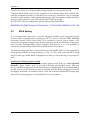
Another Vertical SATA (Port [4]) connector is for dedicated SATA Device with
Internal Power Source support, please reference to AMDY-7000 design. Those SATA
Ports will support A55E ECH native Raid 0, 1,5,10 function on the 5 (Port [0:4]) ports.
For SATA 3 Connector, please reference:
B5048800
(GP).DIP Connector.SATA3-7 Red W/Lock Vertical.ABA-SAT-054-K07.LOTES
For the SATA Port that dedicate for internal powered SATA device, please
reference attached photo from AMDY-7000.
AMDY-7002 User’s Manual
5-2
Appendix B
The CFast is latest (Port [5]) portable storage interface as next generation of
Compact Flash. With native SATA interface on it, it brings faster data transfer rate
and easy installation benefit. So far the CFast is just new on market; a lot of company
is ready for this product. Although the advantage of SATA interface and Read/Write
speed, it still expansive so far. We will include CFAST in design.
For CFAST Connector and Ejector, please reference the 3M model:
B6220280 (GP).SMD Connector.CFast Socket 17+7Pin.N7G24-A0B2RA-10-0HT. 3M
5.2
BIOS Setting
It is assumed that users have correctly adopted modules and connected all the
devices cables required before turning on DC 12V power. 204-pin DDR3 SDRAM,
keyboard, mouse, SATA hard disk, VGA connector, device power cables, ATX
accessories are good examples that deserve attention. With no assurance of properly
and correctly accommodating these modules and devices, it is very possible to
encounter system failures that result in malfunction of any device.
To make sure that you have a successful start with AMDY-7002, it is recommended,
when going with the boot-up sequence, to hit “F2” key and enter the BIOS setup
menu to tune up a stable BIOS configuration so that you can wake up your system far
well.
Loading the default optimal setting
When prompted with the main setup menu, please scroll down to “Load Optimal
Defaults”, press “Enter” and “Y” to load in default optimal BIOS setup. This will
force your BIOS setting back to the initial factory configuration. It is recommended to
do this so you can be sure the system is running with the BIOS setting that Portwell
has highly endorsed. As a matter of fact, users can load the default BIOS setting any
time when system appears to be unstable in boot up sequence.
AMDY-7002 User’s Manual
5-3
Appendix B
Improper disable operation
There are too many occasions where users disable a certain device/feature in one
application through BIOS setting. These variables may not be set back to the original
values when needed. These devices/features will certainly fail to be detected.
When the above conditions happen, it is strongly recommended to check the BIOS
settings. Make sure certain items are set as they should be. These include the COM1/
COM2 ports, USB ports, external cache, on-board VGA and Ethernet.
It is also very common that users would like to disable a certain device/port to
release IRQ resource. A few good examples are
Disable COM1 serial port to release IRQ #4
Disable COM2 serial port to release IRQ #3
Etc…
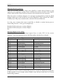
Interrupt Request Lines (IRQ)
Peripheral devices can use interrupt request lines to notify CPU for the service
required. The following table shows the IRQ used by the devices on board.
Interrupt Request Lines IRQ
IRQ#
Current Use
IRQ 0
System ROM
IRQ 1
System ROM
IRQ 2
【Unassigned】
IRQ 3
System ROM
IRQ 4
System ROM
IRQ 5
【Unassigned】
IRQ 6
System ROM
IRQ 7
Unused
IRQ 8
System ROM
IRQ 9
【Unassigned】
IRQ 10
【Unassigned】
IRQ 11
【Unassigned】
IRQ 12
System ROM
IRQ 13
System ROM
IRQ 14
System ROM
IRQ 15
【Unassigned】
Default Use
System Timer
Keyboard Event
Usable IRQ
COM2
COM1
Usable IRQ
Diskette Event
Usable IRQ
Real-Time Clock
Usable IRQ
Usable IRQ
Usable IRQ
IBM Mouse Event
Coprocessor Error
Hard Disk Event
Usable IRQ
It is then very easy to find out which IRQ resource is ready for additional peripherals.
If IRQ resource is not enough, please disable some devices listed above to release
further IRQ numbers.
AMDY-7002 User’s Manual
5-4
Appendix B
5.3
FAQ
Information & Support
Question:I forget my password of system BIOS, what am I supposed to do?
Answer: You can simply short 2-3 pins on JP4 to clean your password.
Note:
Please visit our technical web site at
http://www.portwell.com.tw
For additional technical information, which is not covered in this manual, you can
mail to [email protected] or you can also send mail to our sales, they wull be
very delighted to forward them to us.
AMDY-7002 User’s Manual
5-5