1
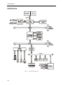
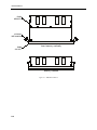
AHIP370 Advanced High Integration Platform with PPGA Celeron® Processor P/N 350370 Ó 1999 XYCOM AUTOMATION, INC. Printed in the United States of America i AHIP370 Manual Revision A Description Manual Released Date 10/99 Trademark Information Brand or product names are registered trademarks of their respective owners. Windows is a registered trademark of Microsoft Corp. in the United States and other countries. Copyright Information This document is copyrighted by Xycom Automation Incorporated (Xycom) and shall not be reproduced or copied without expressed written authorization from Xycom. The information contained within this document is subject to change without notice. Xycom does not guarantee the accuracy of the information and makes no commitment toward keeping it up to date. Xycom Automation 750 North Maple Road Saline, MI 48176–1292 734 - 429-4971 (phone) 734 - 429-1010 (fax) ii Table of Contents Chapter 1 Introduction.............................................................................................................................1-1 Product Overview ...................................................................................................................................1-1 Module Features.....................................................................................................................................1-1 Architecture.............................................................................................................................................1-2 Local Bus Interfaces ...............................................................................................................................1-3 Fast IDE controller.............................................................................................................................1-3 Accelerated Graphics Port (AGP)...........................................................................................................1-3 XGA Graphics Controller ...................................................................................................................1-3 Expansion Options..................................................................................................................................1-4 On-board Memory...................................................................................................................................1-4 DRAM ................................................................................................................................................1-4 Flash BIOS ........................................................................................................................................1-4 Non-volatile SRAM ............................................................................................................................1-4 DiskOnChip 2000 ..............................................................................................................................1-5 Serial and Parallel Ports .........................................................................................................................1-5 Keyboard Interface .................................................................................................................................1-5 Hard and Floppy Drives ..........................................................................................................................1-5 Environmental Specifications..................................................................................................................1-6 Hardware Specifications .........................................................................................................................1-7 Chapter 2 – Installation............................................................................................................................2-1 Configuration Options .............................................................................................................................2-2 Jumpers ..................................................................................................................................................2-2 System Interrupts....................................................................................................................................2-4 DMA Mapping .........................................................................................................................................2-4 Memory Map...........................................................................................................................................2-5 I/O Map ...................................................................................................................................................2-6 Registers.................................................................................................................................................2-8 Register 231h – CPU LED Port ..............................................................................................................2-8 Register 233h – Flash BIOS Control ......................................................................................................2-8 Register 234h - I/O Port Location ...........................................................................................................2-9 I/O Range Select ...............................................................................................................................2-9 Offset Registers....................................................................................................................................2-10 Offset 0 Page Register for Programming (Port Address)................................................................2-10 Offset 1 Page Register for Programming (Port Address +1)...........................................................2-11 Connectors ...........................................................................................................................................2-11 Parallel Port Connector (PARCOM2) ...................................................................................................2-11 Serial Port Connectors..........................................................................................................................2-11 COM1 Connector (COM1)...............................................................................................................2-11 COM2 Connector (PARCOM2) .......................................................................................................2-11 PS/2 Keyboard/Mouse Connector (KBMS1) ...................................................................................2-12 Internal Keyboard Connector (KYBD1)............................................................................................2-12 VGA (Video) Connector (VGA1) ...........................................................................................................2-12 Floppy Drive Connector (FDD1 and FDD2)..........................................................................................2-12 Internal Mouse Connector (MS2)..........................................................................................................2-12 Internal LED Connector (LEDMSC1)....................................................................................................2-12 LED In_Keypad Connector ...................................................................................................................2-12 ISA/IDE Backplane Connector (ATIDE1) .............................................................................................2-13 IDE Connector (HDD1) .........................................................................................................................2-13 Power Connector (PWR1) ....................................................................................................................2-13 iii AHIP370 Manual Touch Control Connector (TCTRL1) ....................................................................................................2-13 Touch Connector (TCH1) .....................................................................................................................2-13 Flat Panel Connector (FPNL1 and FPNL2) ..........................................................................................2-13 Backlight Inverter Connector (DCINV1)................................................................................................2-13 Chapter 3 – BIOS Setup Menus ..............................................................................................................3-1 Moving through the Menus .....................................................................................................................3-1 BIOS Main Setup Menu ..........................................................................................................................3-2 IDE Submenu .........................................................................................................................................3-3 Cache Submenu .....................................................................................................................................3-4 Advanced Menu......................................................................................................................................3-5 I/O Device Configuration Submenu ........................................................................................................3-6 Advanced Chipset Control Submenu......................................................................................................3-7 On-board Socket Site Submenu.............................................................................................................3-8 Flat Panel Submenu ...............................................................................................................................3-8 Security Menu .........................................................................................................................................3-9 Power Menu..........................................................................................................................................3-10 Device Monitoring Submenu.................................................................................................................3-11 Boot ......................................................................................................................................................3-12 Exit Menu..............................................................................................................................................3-13 BIOS Compatibility................................................................................................................................3-13 Appendix A - DRAM Installation............................................................................................................. A-1 Appendix B – Video Modes .................................................................................................................... B-1 Introduction ............................................................................................................................................ B-1 Video Modes.......................................................................................................................................... B-1 Standard Modes .................................................................................................................................... B-1 Extended Modes.................................................................................................................................... B-2 Windows 3.1 .......................................................................................................................................... B-3 Windows ‘95 .......................................................................................................................................... B-4 Appendix C – Pinouts.............................................................................................................................. C-1 VGA Connector (VGA1)......................................................................................................................... C-1 COM1 Connector RS-232/RS-485 (COM1_4) ...................................................................................... C-2 LPT1/COM2 RS-232 Connector (PARCOM2)....................................................................................... C-2 DCIN1 Power Connector (PWR1) ......................................................................................................... C-4 Touch Control Connector (TCTRL1) ..................................................................................................... C-5 Touch Connector (TCH1) ...................................................................................................................... C-6 Internal Mouse Connector (MS2)........................................................................................................... C-6 Internal LED Connector (LEDMSC1)..................................................................................................... C-7 LED In_Keypad Connector (LEDKB1) ................................................................................................... C-7 Flat Panel Connector (FPNL1 and FPNL2) ........................................................................................... C-8 Backlight Inverter Connector (DCINV1)................................................................................................. C-8 Internal Keyboard Connector (KYBD1).................................................................................................. C-9 PS/2 Keyboard/Mouse Connector (KBMS1).......................................................................................... C-9 Internal Floppy Connector (FDD1)......................................................................................................... C-9 External Floppy Connector (FDD2) ..................................................................................................... C-10 IDE Connector (HDD1) ........................................................................................................................ C-11 ISA/IDE Backplane Connector (ATIDE1) ............................................................................................ C-12 PCI Backplane Connector (PCIMG1) .................................................................................................. C-14 Keypad connector (KEYPAD1) ............................................................................................................ C-16 USB Connector.................................................................................................................................... C-16 iv Chapter 1 Introduction Product Overview The Xycom Automation Advanced High-Integration Platform 370 (AHIP370) board is developed expressly for use in Xycom’s line of flat panel industrial personal computers. It is based on the AHIP6 but is optimized in design, layout, and features for use with flat panel computer systems. This integrated design approach allows Xycom industrial PC/ATs to incorporate “Big PC” features in an extremely compact package. These “Big PC” features include AGP video PCI/ISA expansion, Celeron CPU, full-size hard disk, status LEDs, infrared port, and integrated touchscreen. Module Features · Supports · 66 MHz and 100 MHz front side bus · Intel Celeron® processors (PPGA package) · 32 MB - 256 MB DRAM DIMMs · AGP local bus XGA graphics with 2 MB integrated DRAM · Up to 1024x768\256 colors non-interlaced · 640x480x256K, 800x600x64K, 1024x768x256 color TFT panels · PCI fast IDE controller · Two 16550-compatible serial ports · COM 1 is RS-232, or RS-485 · COM 2 is RS-232 port, or Infrared (IR or IrDA), or Touchscreen · Centronics-compatible parallel port · Floppy Controller (only one floppy supported) · Internal FFC connector · External connector · Touchscreen interface (COM 2 or PS/2 mouse port) · PS/2 keyboard port · Real time clock and battery · Disk on a chip supported (DOC 2000) · 32Kx8 and 128Kx8 nonvolatile RAM supported · LED interface · Designed specifically for Xycom Automation industrial PC/ATs. 1-1 AHIP370 Manual Architecture Figure 1-1. AHIP370 Block diagram 1-2 Local Bus Interfaces The Celeron design uses the 440BX chip set. The 440BX integrates a high performance interface from PCI to IDE. This interface is capable of accelerated data transfers. The 440BX chipset provides an accelerated PCI-to-ISA interface that includes · A high-performance enhanced IDE controller · PCI and ISA master/slave interfaces · Plug-and-play port for on-board devices The chipset also provides many common I/O functions found in ISA-based PC systems, including: · Seven-channel DMA controller · Two 82C59 interrupt controllers · 8254 timer/counter · Control logic for NMI generation Fast IDE controller The high-speed local bus IDE controller supports programmed I/O modes 0-4. It also provides 4x32-bit read-ahead buffer and 4x32-bit write-post buffer support to enhance IDE performance. Accelerated Graphics Port (AGP) XGA Graphics Controller The AGP bus controller supports CRT displays and flat panel displays with 2 MB video memory. The controller also supports resolutions of 640x480, 800x600, and 1024x768 with 64K colors. 1-3 AHIP370 Manual Note The IDE controller supports enhanced PIO modes, which reduce the cycle times for 16-bit data transfers to the hard drive. Check with your drive manual to see if the drive you are using supports these modes. The higher the PIO mode, the shorter the cycletime. Select the PIO modes in the BIOS setup (refer to Chapter 3). The autoconfigure classifies the drive connected if the drive supports the auto ID command. If you experience problems, change the PIO to standard. Expansion Options The AHIP370 offers expansion when used in conjunction with a Xycom Plug-in Expansion Backplane. This gives the user a total of six full length slots: · Four dedicated ISA slots · One dedicated PCI slot · One slot that can be either ISA or PCI On-board Memory DRAM The AHIP370 has two 168-pin DIMM memory sites, providing up to 256 MB of SDRAM (with up to 512 MB capability in the future). The memory site is populated by 100 MHz synchronous DRAM. Flash BIOS The AHIP370 board uses a Flash BIOS. Flash is used for system BIOS and video BIOS. Non-volatile SRAM The AHIP370 hardware supports non-volatile SRAM. Contact Xycom Automation at 1-800-AT-XYCOM (1-800-289-9266) for additional information about this feature. The SRAM comes in a module type package and contains a built-in battery and battery backup circuitry. The battery life is approximately seven years in the absence of VCC. The SRAM supports 32Kx8 and 128Kx8 memory sizes. The RAM comes in a 32 pin dip (0.6 inches wide) standard format. SRAM can be located at: CC000, D0000, or D8000. 1-4 DiskOnChip 2000 The DiskOnChip 2000 is a single-chip Flash disk in a standard 32-pin DIP format. It requires an 8 Kbyte window to view as an extension BIOS. During boot up, the DiskOnChip loads its software in the PC’s memory and installs itself as an additional drive. Serial and Parallel Ports PC/AT peripherals include two high-speed, RS-232, 16550-compatible serial ports and one bi-directional Centronics-compatible parallel port: · COM 1 of the serial ports accepts either RS-232 or RS-485 connections. · COM 2 is RS-232 (stacked DB 25) with parallel port. The COM2 port can be used for one of three options: · Serial port out the 25 pin DB connector · Touchscreen controller interface · Infrared (IrDA) interface The BIOS setup is used to configure the port as a serial port or IrDA port. This port can be used as both a serial interface and an IR interface, by allowing software to control the connection. If the touchscreen controller is jumpered to use COM2, the 25-pin DB connector must not be used to interface to a device. These lines are combined internally. The BIOS setup menu for COM2 must be set to standard operation to use the touchscreen controller on COM2. Keyboard Interface The keyboard interface uses a standard PS/2-style connector. A polyswitch protects the +5 V. This device opens if the +5 V is shorted to GND. Once you remove the shorting condition, the polyswitch allows current flow to resume. Hard and Floppy Drives The floppy interface supports one floppy drive. The AHIP370 can interface to a floppy via the on-board floppy connector or the external floppy connector. In order to connect a floppy drive to the external connector after power up, the floppy drive must be setup for a 1.44 MB drive and the floppy drive test must be disabled. If this is not done the system generates a floppy drive error during the POST (Power On Self Test). The enhanced IDE (EIDE) interface supports up to 2 hard drives. Hard drive interface is via the Xycom plug-in backplane or the on-board IDE controller. 1-5 AHIP370 Manual Caution The higher the PIO mode, the shorter the cycletime. As the IDE cable length increases, this reduced cycle time can lead to erratic operation. The total IDE cable length must not exceed 18 inches. If two IDE drives are connected, they must not be more than six inches apart. Environmental Specifications Table 1-1. Environmental Specifications Characteristic Temperature Operating Non-operating Humidity Operating Non-operating Altitude Operating Nonoperating Vibration a (3512, 3515 systems b) Operating Nonoperating Specification 0° to 55° C (32° to 140° F) -40° to 85°C (-40° to 185°F) 20% to 80% RH noncondensing 20% to 80% RH noncondensing Sea level to 10,000 feet (3048 m) Sea level to 50,000 feet (15240 m) 5 to 55Hz 0.006” peak to peak displacement 56-2000 Hz 1.0g maximum acceleration 5-55 Hz 0.006” peak to peak displacement 56-2000 Hz 2.5 g maximum acceleration Shock a (3512, 3515 systems b) 15g peak acceleration, 11 msec duration Operating Nonoperating 30g peak acceleration, 11 msec duration a These values are with solid state hard drives and NOT rotating media drives b Consistent with system level specifications. See your system manual if you have a system other than the 3512 or 3515 models. 1-6 Hardware Specifications Table 1-2. Hardware Specifications Characteristic Power Specifications: The CPU power supply on the AHIP370 provides a voltage range of 1.30V to 2.05V in increments of 50mV. The CPU selects its voltage through its four outputs VID3VID0. The supply was changed to accommodate future Socket370 CPUs which will run at lower voltages. CPU speed AGP Super VGA Graphics Controller Serial Ports (2) Parallel Interface On-board memory Specification The maximum current that the supply can deliver is 19A. 300 MHz, 366 MHz, and 433 MHZ 640x480, 800x600, and 1024x768, 64K colors maximum resolution 2 MB video DRAM COM1 is RS-232 or RS-485 COM2 is RS-232, or IR, or Touchscreen Both 16550 compatible Centronics compatible Up to 256 MB; 66 MHz SDRAM 1-7 Chapter 2 – Installation This chapter provides information on configuring the AHIP370 Processor Module. Pinouts for the connectors are located in Appendix C. Figure 2-1 illustrates the jumper and connector locations on the AHIP370. BACKLIGHT INVERTER CONN. TOUCH CONTROL CONN. INTERNAL MOUSE CONN. LED IN KEYPAD CONN. TOUCH CONN. KEYPAD CONN. COM2 RS-232 (TOP) PARALLEL (BOTTOM) CONNS. COM1 RS-485 (TOP) RS-232 (BOTTOM) CONNS. CPU FAN CONN. FLAT PANEL CONN. EXTERNAL MOUSE (TOP) KEYBOARD (BOTTOM) CONNS. USB CONN. SYSTEM FAN CONN. VIDEO CONN. HDD1 CONN. INTERNAL FLOPPY CONN. EXTERNAL INTERNAL KEYBOARD FLOPPY CONN. CONN. LED CONN. ATI/IDE1 BACKPLANE CONN. POWER CONN. Figure 2-1. AHIP370 Jumper and Connector Locations 2-1 AHIP370 Manual Configuration Options Jumpers The following tables list AHIP370 jumpers, their default positions and their functions. The jumpers marked “Access” are placed at the top of the board for easy customer access. Table 2-1. AHIP370 Jumpers Jumper J1 Position A B A B A B A B A B A B A B A B J2 J3 J4 J7 J8 J9 J18 Function Push button reset switch DISABLED (Access) Push button reset switch ENABLED CMOS OK (Access) Clear CMOS Flat panel selected (Access) CRT selected Normal Program the H8 Boot flash enabled Boot ROM enabled Enables RS-485 port in the assertive state. Enables RS-485 port in the negated state. DTR used to control the RS-485 port RTS used to control the RS-485 port VGA ENABLED VGA DISABLED The BIOS recovery scheme used on the AHIP6 utilizes a jumper (J5) to select recovery mode. The FPGA at U15 uses this to define the state of address signal A18 into the flash chip. According to the following table: J5* A B Mode Normal Recovery Flash A18 state Inverted Not Inverted *Recent changes in flash technology have mandated that J5 be in the B position for normal operation. This is confusing, as it is contrary to the design documentation and user manual. Because of this, J5 has been eliminated on the AHIP370. A 1K pull-down resistor is connected to signal XD (4) to simulate the B position. 2-2 Chapter 2 – Installation The following table outlines the changes in jumper configurations between the AHIP370 and AHIP6: Table 2- 2. Changes in Jumper Configuration AHIP6 Jumper J6, 14, 15, 16, 17 AHIP370 Jumper N/A J1 J1 J2 J2 J3 J3 J4 J4 J5 N/A J7 J7 J18 N/A N/A J8 N/A J9 J8 J10 J19 J11 Description Controls the speed of the CPU A PB reset disabled B PB reset enabled A CPU will not clear CMOS on power up B CPU will clear CMOS A Flat panel enabled B CRT port enabled A Normal operation B Puts H8 in program mode A Normal flash boot B Recovery flash boot A CPU boots from flash B CPU boots from ROM A Onboard video enabled B Onboard video disabled A The asserted state will enable the RS-485 port. B The negated state will enable the RS-485 port. A DTR is used to control the RS-485 port. B RTS is used to control the RS-485 port. Used to program Lattice component. Connecting the two pins will reset the CPU. Comments The socket370 implementation by Intel calls for the CPU to define its own speed and not be determined by jumpers. There are no jumpers on the AHIP370 for this purpose. PB refers to an external pushbutton that may be connected through the RS-232 interface. See above. The video is always enabled on the AHIP370. If an external VGA adapter is plugged into the system, the BIOS will disable the onboard chip. Refers to the state of the modem control signal selected by J9. J8 and J9 function together to control the RS485 port. RS-485 TriState Control On the AHIP6, the RS-485 is enabled by asserting DTR. Two jumpers were added to the AHIP370 to allow either DTR or RTS to control the RS-485 drives and determine whether the asserted or negated state will enable it. Factory use only. Factory use only for emulators. 2-3 AHIP370 Manual N/A J12 Forces front-side bus to run at 66MHz. Factory use only. All AHIP370 jumpers are factory set in the "A" position. System Interrupts The following table describes the interrupts used on the AHIP370. Table 2- 3. System Interrupts Interrupt IRQ0 IRQ1 IRQ2 IRQ3 IRQ4 IRQ5 IRQ6 IRQ7 IRQ8 IRQ9 IRQ10 IRQ11 IRQ12 IRQ13 IRQ14 IRQ15 Function System Timer Keyboard Cascade Serial Port* Serial Port* Parallel Port* Floppy Controller Parallel Port* Real Time Clock Unused Serial Port* Serial Port* Mouse Port Math Co Fixed Disk Unused * BIOS setup controlled The BIOS setup menu controls the interrupts for the serial and the parallel port. The two Serial ports on the AHIP370 board can be mapped to any two of the following interrupts: 3, 4, 10, & 11 (defaults are interrupts 3 and 4). One parallel port can be mapped to IRQ5 or IRQ7. The BIOS setup menu is used to control the location and interrupts for the serial and parallel ports. Note The BIOS controls the mapping of the AGP interrupts to AT-bus interrupts. This means if a AGP device is plugged into a slot and needs an interrupt, one of the AT-bus interrupts must be mapped to the AGP interrupt. DMA Mapping Table 2-4. DMA Channels 2-4 Chapter 2 – Installation DMA DMA0 DMA1 DMA2 DMA3 DMA5 DMA6 DMA7 Function Unused (Could be used for EPP/ECP parallel port option) Unused Floppy Controller Unused (Could be used for EPP/ECP parallel port option) Unused Unused Unused DMA channels 0-3 are 8-bit and DMA channels 5-7 are 16-bit. When the ECP option is enabled, one of the 8-bit DMA channels is used. Memory Map The following table shows the AHIP370 memory map. The I/O designation refers to memory viewed as part of the AT bus. Table 2- 5. Memory Map Address Range (HEX) FFFE0000 - FFFFFFFF end of DRAM - FFFDFFFF 00100000 - end of DRAM 000F0000 - 000FFFFF 000E0000 - 000EFFFF 000D0000 - 000DFFFF 000C0000 - 000CBFFF 000A0000 - 000BFFFF 00000000 - 0009FFFF Size 128K xxxK xxxK 64K 64K 64K 48K 128K 640K Device SYSTEM BIOS I/O Memory DRAM* SYSTEM BIOS SYSTEM BIOS AT bus I/O VGA BIOS VGA DRAM MEMORY DRAM *See Intel 430BX data sheet for a description of optional settings for assigning memory holes or gaps within memory map area. 2-5 AHIP370 Manual I/O Map The I/O map for the AHIP370 in Table 2- 6 contains all the I/O ports of the IBM AT architecture with some additions. Table 2- 6. I/O Map Hex Range 000-01F 020-021 022-024 025-02F 040-05F 060-06F 070-07F 080-091 092 93-9F 0A0-0BF 0C0-0DF 0F0 0F1 0F2-0F3 0F4 0F5-0F7 0F8 0F9-0FB 0FC 0FD-0FF 100 102 103-179 180-181 182-1EF 1F0-1F7 1F8-22F 231 233 234 278-27F 280-2F7 2F8-2FF 300-36F 370-377 378-37F 380-3AF 3B0-3BB 2-6 Device DMA controller 1, 8237A-5 equivalent Interrupt controller 1, 8259 equivalent Available Interrupt controller 1, 8259 equivalent (see Note 3) Timer, 8254-2 equivalent 8742 equivalent (keyboard) Real Time Clock bit 7 NMI mask (see Note 3) DMA page register (see Note 3) Reset/ Fast Gate A20 DMA page register (see Note 3) Interrupt controller 2, 8259 equivalent (see Note 3) DMA controller 2, 8237A-5 equivalent (see Note 3) N/A N/A N/A IDE ID port N/A IDE Index port N/A IDE Data port N/A Available C&T Global enable register Available SRAM control register (May be remapped based on I/O port 234h) Available IDE Controller (AT Drive) Available Xycom LED port Xycom Flash control register Xycom IO port control register Parallel Port 2 (see Note 1) Available Serial Port 2 (see Note 1) Available Alt. Floppy Disk Controller (see Note 1) Parallel Port 1 (see Note 1) Available mono mode video Chapter 2 – Installation Hex Range 3BC-3BF 3C0-3CF 3D0-3DF 3E0-3EF 3F0-3F7 3F8-3FF CF8 CFC Device reserved for parallel port VGA registers (see Note 2) CHIPS flat panel & color mode registers Available Primary Floppy disk controller Serial port 1 (see Note 1) AGP configuration address register (see Note 4) AGP configuration data register (see Note 4) Note 1 Since serial and parallel port addresses can be changed or the port may be disabled, these addresses can be used for some applications and not for others. Note 2 Reference the C&T69000 advance data book for detailed information. Note 3 Reference the Intel 430BX chip set data book for detailed information. Note 4 Reference the following for AGP configuration: AGP local bus specification rev 2.1, Intel 430BX chip set data book, and C&T69000 data book. 2-7 AHIP370 Manual Registers The AHIP370 contains five I/O ports: 231h, 233h, 234h, and a user-definable port (port 180/1h, 2E0/1h, 3E0/1h, or 300/1h). These ports are compatible with AHIP4+ and AHIP 6+. Register 231h – CPU LED Port Register 231h controls the LEDs and signals shown in the following table. Table 2- 7. Register 231h - CPU LED Port Bit 0 1 2 3 4 5* 6 7 LED/Signal Reserved Reserved Reserved Reserved Reserved ENFLASHWR VGA_EN CLRCMS Result 0 0 0 0 0 1 = Enables Flash write 1 = Enables on-board VGA 1 = CMOS okay 0 = Clear CMOS R/W R R R R R R/W R R *Note: This bit must be 1 to make FLASH visible @D0000h when booting from AT bus. This bit also enables the FLASH @C0000h when booting to FLASH. Register 233h – Flash BIOS Control Register 233h controls the signals shown in the following table. Table 2- 8. Register 233h - Flash BIOS Control Register Bit 0 1 2 3 4 5 6 7 2-8 Signal FLA15 FLA16 FLA17 FLA18 FPSEL0 FPSEL1 FPSEL2 FPSEL3 Result Flash address 15 - page control bit Flash address 16- page control bit Flash address 17 - page control bit Flash address 18 - page control bit Flat panel select bit 0 Flat panel select bit 1 Flat panel select bit 2 Flat panel select bit 3 R/W R/W R/W R/W R/W R R R R Chapter 2 – Installation Register 234h - I/O Port Location Register 234h controls the I/O port location register shown in the following table. Table 2- 9. Register 234h - I/O Port Location Register Bit 0 1 2 3 4 5 6 7 Signal Reserved Reserved Reserved Reserved I/O range select I/O range select I/O port bit 0 I/O port bit 1 Result 0 0 0 0 I/O range select bit 0 I/O range select bit 1 I/O port bit 0 I/O port bit 1 R/W R R R R R R R/W R/W Bits 0-3 are reserved for the temperature sensor. Bits 4 and 5 are reserved for setting the memory location for the SRAM. I/O Range Select The following are ranges defined by register 234h. Table 2- 10. I/O Range Selection I/O range selection 00 01 10 11 Range no range CC000-CFFFF D0000-D7FFF D8000-DFFFF 2-9 AHIP370 Manual Offset Registers The following registers are located starting at the I/O location defined by register 234h. Table 2- 11. I/O Port Selection (Port Address) I/O port selection 00 01 10 11 Port address 180h 2E0h 3E0h 300h Offset 0 Page Register for Programming (Port Address) Offset 0 is a read-only register that checks the battery status Table 2- 12. Offset 0 Page Register for Programming (Port Address) 2-10 Bit 0 Signal Battery status 1 2 3 4 5 6 7 Reserved Reserved Reserved Reserved Reserved Reserved Reserved Result 0 = battery good 1 = battery fail 0 0 0 0 0 0 0 R/W R R R R R R R R Chapter 2 – Installation Offset 1 Page Register for Programming (Port Address +1) Offset 1 controls the paging bits for the ROM. This feature is needed for programming flash. Table 2- 13. Offset 1 Page Register for Programming (Port Address +1) Bit 0 1 2 3 4 5 6 7 Signal Control ROM/RAM15 Control ROM/RAM16 Control ROM/RAM17 Reserved Reserved Reserved Reserved Reserved Result ROM address 15-page control bit ROM address 16-page control bit ROM address 17-page control bit 0 0 0 0 0 R/W R/W R/W R/W R R R R R Connectors This section describes the connectors for the AHIP370. Appendix C provides the pinouts for each of the connectors. Parallel Port Connector (PARCOM2) The parallel port is a stacked DB 25-pin connector. Serial Port Connectors There are two serial ports supported on the AHIP370 board. COM1 Connector (COM1) The COM1 is a nine pin connector consisting of two connectors attached to one logical port. Only one connector can be used at a time, either the RS-232 port or the RS-485 port. COM2 Connector (PARCOM2) The COM2 connector is a male DB 25-pin connector. This port can be used for three separate devices (but only one at a time): · Touch screen controller · IrDA interface 2-11 AHIP370 Manual · LPT1/COM2 RS-232 connector The BIOS setup determines whether the COM2 is used for the RS-232 connector or the IR interface. Jumpers on the touchscreen controller select the COM2 port or the auxiliary port. If a touchscreen controller is jumpered for COM2, this COM port is not available. PS/2 Keyboard/Mouse Connector (KBMS1) This double stacked connector provides an upper and lower connector for the keyboard and mouse port. Internal Keyboard Connector (KYBD1) This is a five-pin internal keyboard connector on the motherboard. VGA (Video) Connector (VGA1) The VGA (Video) connector is a 15-pin connector located on the I/O panel. This connector is only enabled when J3 is in position B or no flat panel is connected to the CPU board. Floppy Drive Connector (FDD1 and FDD2) There is an internal floppy connector (FDD1) and an external floppy connector (FDD2). The floppy interface supports only one floppy drive. The floppy drive connector is a 26-pin connector. Both of these ports use a polyswitch to protect VCC from directly shorting to GND. Internal Mouse Connector (MS2) This four-pin connector provides a future method to integrate a mouse to the front panel. Internal LED Connector (LEDMSC1) This 20-pin connector provides a low cost method to add LED’s to the touch only units, and also provides the pinout for the IR interface port. LED In_Keypad Connector This connector is used for future designs which support the LEDs in the keypad. 2-12 Chapter 2 – Installation ISA/IDE Backplane Connector (ATIDE1) The ISA/IDE Backplane connector is a 120-pin connector. This connector provides both ISA and IDE signals to the backplane. IDE Connector (HDD1) IDE hard drive connector is a 40-pin header. This header is intended for future options and testing. Power Connector (PWR1) This 20-pin connector is a standard ATX style PC power supply connector. Touch Control Connector (TCTRL1) This 40-pin connector supports 5-wire touchscreens. The connector is latching to provide for a DRAM SIMM type installation. Touch Connector (TCH1) The five-pin touch connector is the interface to the touch panel. Flat Panel Connector (FPNL1 and FPNL2) The flat panel connector is a 60pin SMD through board connector. The four flat panel select lines define up to 16 unique panel types. If all signals are high (no cable attached) the system defaults to CRT. The system board supports +5V and 3.3V TFT panels with a custom flat cable. It supports STN panels with a 2.5” X 2.75” PCB which contains the DC/DC for the custom VEE voltage along with the contrast and power sequencing circuit. There are also provisions to support a temperature sensor for automatic contrast control. Backlight Inverter Connector (DCINV1) This 8-pin connector provides power for the backlight inverter. 2-13 Chapter 3 – BIOS Setup Menus The AHIP370 board’s customized BIOS has been designed to surpass the functionality provided for normal PC/ATs. This custom BIOS allows you to access the value-added features on the AHIP370 module without interfacing to the hardware directly. Moving through the Menus General instructions for navigating through the screens are described below: Key F1 or ALT-H F2 ESC ¬ or ® arrow keys or ¯ arrow keys TAB or SHIFT + TAB Result General Help window Enters the menu Exits the menu Selects a different menu Moves the cursor up or down HOME or PGUP Cycles the cursor up or down Moves the cursor to the top of the window END or PGDN Moves the cursor to the bottom of the window F5 or F6 or + or SPACE F9 F10 Selects the previous value for the field ENTER Executes the Command or Select ? Submenu or displays a pop up menu Refresh screen ALT-R Selects the next value for the field Loads the default configuration values for the menu Saves and Exits Note An asterisk (*) indicates fields which may or my not be visible (depending on the option selected different fields may appear). To select an item, use the arrow keys ¯ ¬® to move the cursor to the field you want. Then use the + and - keys to select a value for that field. For many fields, pressing ENTER displays a pop-up menu of all valid choices for the field. An “?” beside a field indicates the presence of a submenu. To enter the submenu, use the arrow keys to select the field and then press ENTER. 3-1 AHIP370 Manual BIOS Main Setup Menu You start the BIOS Setup utility as your system boots up. To access the main menu, press F2 after the memory tests and before your system loads the operating system. If the setup prompt is enabled on your system, the BIOS will display the following message: “Press F2 to enter Setup.” Xycom BIOS Setup Utility Main Advanced Security Power Boot Exit Item Specific Help System Time: [16:19:20] System Date: [10/27/98] Diskette A: [1.44 MB, 3½”] If the line item you Diskette B: [Disabled] are viewing has ?IDE Primary Master: (1082 MB) be listed here. ?IDE Primary Slave: (CD-ROM) ?IDE Secondary Master: [None] ?IDE Secondary Slave: [None] System Memory: 640 KB Extended Memory: 31744 KB ?Cache RAM [512 KB] specific help, it will F1 Help ¯ ESC Exit ¬® Select Menu Select Item -/+ Change Values Enter Select » Submenu F9 Setup Defaults F10 Save and Exit Figure 3-1. Main Setup Menu Table 3-1. Main Setup Menu Options Option System Time (HH/MM/SS) System Date (MM:DD:YYYY) Diskette A or B 3-2 Description Sets the real-time clock for hour, minute, and seconds. The hour is calculated according to a 24-hour military clock (i.e., 00:00:00 through 23:59:59). Use TAB to move right; SHIFT + TAB to move left. The ENTER key may be used to move from one field to the next. The numeric keys, 0-9, are used to change the field values. It is not necessary to enter the seconds or type zeros in front of numbers. Sets the real-time clock for the month, day, and year. Use TAB to move right; SHIFT + TAB to move left. The ENTER key may be used to move from one field to the next. The numeric keys, 0-9, are used to change the field values. It is not necessary to type zeros in front of numbers. Selects the floppy disk drive installed in your system. Chapter 3 – BIOS Setup Menus Option IDE Primary Master IDE Primary Slave IDE Secondary Master IDE Secondary Slave System Memory Description These items show the IDE configuration and allow entry into the IDE submenus. Displays the amount of conventional memory detected during boot-up. This field is not user configurable. Displays the amount of extended memory detected during boot-up. This field is not user configurable. Displays the amount of cache detected and allows entry into the cache submenu. Extended Memory Cache RAM IDE Submenu Xycom BIOS Setup Utility Main IDE Primary Master (C: 1082 Mb) Type: Item Specific Help [Auto/User] * Cylinders: [ 2097] If the line item you * Heads: [ 16] are viewing has * Sectors [ 63] specific help, it will * Maximum Capacity 1082 Mb * Multi-Sector Transfers: [8 Sectors] * LBA Mode Control: [Enabled] * 32-Bit I/O: [Disabled] * Transfer Mode: [Fast PIO 4] * Ultra DMA Mode [Disabled] F1 Help ¯ ESC Exit ¬® Select Menu Select Item be listed here. -/+ Change Values Enter Select » Submenu F9 Setup Defaults F10 Save and Exit Figure 3-2. IDE Adapter Submenu The IDE submenus are used to configure IDE hard drive information. If only one drive is attached to an IDE adapter, then only the parameters in the Master Submenu need to be entered. If two drives are connected, both Master and Slave Submenu parameters will need to be entered. All IDE submenus contain the same information and operate the same. Table 3-2. IDE Adapter Submenu Options Option Type 1, 2 3-3 Cylinders Description Options include Auto, None, CD-ROM, other ATAPI, and User. “Auto” autotypes at each boot. “None” indicates no device is attached. “CD-ROM” indicates that a CD-ROM drive is attached. “Other ATAPI” indicates that a removable disk drive is attached. “User” allows the user to specify device parameters. Indicates the number of cylinders on the hard drive. This information is automatically entered if Type is set to “Auto.” AHIP370 Manual Option 1, 2 Heads Description Indicates the number of read/write heads on the hard drive. This information is automatically entered if Type is set to “Auto.” 1, 2 Sectors Indicates the number of sectors per track on the hard drive. This information is automatically entered if Type is set to “Auto.” 1 Maximum Capacity Indicates the maximum storage capacity of the drive. 3, 4 Multi-Sector Sets the number of sectors per block. Options are Auto, 2, 4, 8, or 16 sectors. “Auto” Transfers sets the number of sectors per block to the highest number supported by the drive. 3, 4 LBA Mode Control Enables Logical Block Access. The default is disabled and should work with most hard drives. 3 32-Bit I/O Enables 32-bit communication between CPU and IDE interface. 3, 4 Transfer Mode Selects the method for transferring the data between the hard disk and system memory. The drive type and cable length determine available options. 3, 4 Ultra DMA Mode Enables or disables the maximum storage capacity of the drive. 1 = Visible only when type is “Auto” or “User” 2 = Editable only when Type is “User” 3 = Not visible when Type is set to “None” 4 = Not editable when Type is set to “Auto” Cache Submenu Xycom BIOS Setup Utility Main Memory Cache Item Specific Help Memory Cache: [Enabled] If the line item you Cache System BIOS area: [Write Protect] are viewing has Cache Video BIOS area: [Write Protect] specific help, it will Cache Base 0-512K [Write Back] be listed here. Cache Base 512K-640K: [Write Back] Cache Extended Memory Area: [Write Back] Cache Extended Memory Region CC00-CFFF [Disabled] D000-D3FF [Disabled] D400-D7FF [Disabled] D800-DBFF [Disabled] DC00-DFFF [Disabled] F1 Help ¯ ESC Exit ¬® Select Menu Select Item -/+ Change Values Enter Select » Submenu F9 Setup Defaults F10 Save & Exit Figure 3-3. Memory Cache Submenu Enabling cache increases CPU performance by holding data most recently accessed in a special high-speed static RAM area called cache. The AHIP370 provides two levels of cache memory; level one is 16 K 3-4 Chapter 3 – BIOS Setup Menus internal to the Pentium processor, and level two, or external cache, is the cache-on-a-stick site (COAST) which can accommodate 256 or 512 K of high-speed cache memory. Table 3-3. Memory Cache Submenu Options Option Memory Cache Cache System BIOS Area Description Controls the state of Pentium II memory cache. Allows the system BIOS memory area to be cached if enabled. Enabling also increases system performance. The default is enabled and write protected. Allows the video BIOS memory area to be cached if enabled. Enabling also increases system performance. The default is enabled and write protected. Controls caching of 512K base memory. Default is Write Back Caching. Controls caching of 512K and 640K base memory. Default is Write Back Caching. Controls caching of system memory above 1 MB. Default is Write Back Caching. Caches the corresponding memory when enabled. Memory in this area is usually extended BIOS or AT-bus memory. Enabling cache may increase system performance, depending on how the extended BIOS is accessed. The default is disabled. Cache Video BIOS Area Cache 0 - 512K Cache 512K - 640K Cache Extended Memory Area Cache Memory Region Advanced Menu Xycom BIOS Setup Utility Main Advanced Security Exit Item Specific Help ?I/O Device Configuration If the line item you are ?Advanced Chipset Control viewing has specific help Installed O/S [other] Reset Configuration Data [No] Large Disk Access Mode [DOS] Local Bus IDE adapter [Both] it will be listed here. ?On-board Socket Site ?Flat Panel F1 Help ¯ ESC Exit ¬® Select Menu Select Item -/+ Change Values Enter Select » Submenu F9 Setup Defaults F10 Previous Values Figure 3-4. Advanced Setup Menu This menu allows you to change the peripheral control, advanced chipset control, and disk access mode. Table 3-4. Advanced Menu Option Feature I/O Device Configuration Advanced Chipset Control 3-5 Description Allows entry into the I/O submenu. Allows entry into the chipset submenu. AHIP370 Manual Installed O/S Reset Configuration Data Large Disk Access Mode Local Bus IDE Adapter On-board Socket Site Flat Panel Select "Win95" if you are using an operating system with Plug & Play capabilities. Default is [Other]. Used to reset the Plug & Play configuration data table when new devices are added/removed or whenever the BIOS is upgraded. Select “DOS” if your system has DOS. Select “Other” if you have another operating system, such as UNIX. A large disk is one that has more than 1024 cylinders, more than 16 heads, or more than 63 tracks per sector. Controls configuration of local bus IDE adapter. Default is [Both] (primary and secondary). Allows entry into socket site submenu. Allows entry into flat panel submenu. I/O Device Configuration Submenu Xycom BIOS Setup Utility Advanced I/O Device Configuration Item Specific Help COM A: [Auto] Base I/O Address [3F8] If the item you Interrupt [IRQ4] are viewing has COM B: [Auto] be listed here. Mode: [Normal] Base I/O Address [2F8] Interrupt [IRQ3] Parallel port: [Auto] Mode [Bi-directional] Base I/O Address: [378] Interrupt [IRQ7] Floppy Disk Controller [Enabled] Base I/O Address [Primary] specific help, it will F1 Help ¯ ESC Exit ¬® Select Menu Select Item -/+ Change Values Enter Select » Submenu F9 Setup Defaults F10 Previous Values Figure 3-5. Integrated Peripherals Submenu The I/O Device Configuration submenu is used to configure the COM ports, parallel ports, and enable/disable the diskette and enhanced IDE controllers. Table 3-5. Integrated Peripherals Submenu Options Option COM A COM B Parallel Port 3-6 Description Allows the COM A port to be enabled, disabled, or autoselected. Allows the COM B port to be enabled, disabled, or autoselected. Allows the parallel port to be enabled, disabled, or autoselected. Chapter 3 – BIOS Setup Menus Option Description Floppy Disk Controller Allows the floppy drive controller to be enabled, disabled, or autoselected. 1 Base I/O Address Select a unique address for the corresponding peripheral. 1 Interrupt Select an interrupt request for the corresponding peripheral. 1 Mode Controls the protocol for the corresponding peripheral. 1 = Visible only when corresponding peripheral is “Enabled” Advanced Chipset Control Submenu Xycom BIOS Setup Utility Advanced Advanced Chipset Control Enable Memory Gap Item Specific Help [Disabled] If the item you ECC Config: [Disabled] are viewing has SERR Signal Condition: [Multiple bit] specific help, it will 8-bit I/O Recovery: [3.5] be listed here. 16-bit I/O Recovery: [3.5] F1 Help ¯ ESC Exit ¬® Select Menu Select Item -/+ Change Values Enter Select » Submenu F9 Setup Defaults F10 Save & Exit Figure 3-6. Advanced Chipset Control Submenu This menu allows you to change the values in the chipset registers and optimize your system’s performance. Note Most system configurations will work best with these options in their default configurations. Fast processors may cause I/O failures at the default recovery values. You can increase the number of cycles when encountering this problem; however, slowing down the clock too much may cause I/O initialization problems. You should increase the number of clock cycles incrementally, until you see an improvement in I/O performance. Table 3-6. Advanced Chipset Control Submenu Options Option Enable Memory Gap ECC Configuration SERR Signal Conditions 8-bit I/O Recovery 16-bit I/O Recovery 3-7 Description Allows creation at a 128K memory gap in conventional memory from 512K to 640K, or a 1MB memory gap in extended memory from 15 MB to 16 MB. Requires use of conventional or extended memory. Default is [Disabled]. Allows configuration of Error Checking and Correction Memory. Requires ECC memory. Default is [Disabled] Allows configuration of conditions upon which the SERR signal is to be asserted for ECC memory. Requires ECC memory. Default is [Multiple bit]. Number of ISA clock cycles inserted between back-to-back I/O operations. AHIP370 Manual On-board Socket Site Submenu Xycom BIOS Setup Utility Advanced On-board Socket Site Item Specific Help 32-pin Socket Site Address [Disabled] *32-pin Socket Site Type 32-pin Socket Site I/O If the item you [SRAM] are viewing has [180h-181h] specific help, it will be listed here. F1 Help ¯ ESC Exit ¬® Select Menu Select Item -/+ Change Values F9 Enter Select » Submenu Setup Defaults F10 Previous Values Figure 3-7. On-board Socket Site submenu Table 3-7. On-board Socket Site submenu options Option 32-pin Socket Site Address Description Allows on-board 32-pin socket site to be disabled or mapped to a memory range. Default is [Disabled]. 1 32-pin Socket Site Type Indicates type of memory installed in on-board 32-pin socket site. Default is [SRAM]. 32-pin Socket Site I/O Allows configuration of I/O address used by on-board 32-pin socket site. Default is [180h-181h]. 1 = Visible only when Socket Site Address is “Enabled” Flat Panel Submenu Xycom BIOS Setup Utility Advanced Flat Panel Item Specific Help Default Panel Type 640 x 480 STN If the item you Video Screen Expansion [ON] are viewing has Simultaneous Video [Disabled] specific help, it will be listed here. F1 Help ¯ ESC Exit ¬® Select Menu Select Item -/+ Change Values Enter Select » Submenu F9 Setup Defaults F10 Previous Values Figure 3-8. Flat Panel submenu Table 3-8. On-board Socket Site submenu options Option Default Panel Type 3-8 Description Displays video BIOS configuration. Not editable. Automatically updates when flat panel changes. Chapter 3 – BIOS Setup Menus Option Video Screen Expansion Description Enables video screen expansion to fill the area of the flat panel screen. Used most for DOS, the setting for each option depends on the type of flat panel attached to the unit. “ON” maximizes expansion as allowed for the panel, while “OFF” minimizes expansion as allowed for the panel. Select “Enabled” if you want video on an external CRT monitor and on the unit’s flat panel display. Select “Disabled” if you want only the flat panel display. Not editable if default panel type does not support simultaneous video. Simultaneous Video Security Menu PhoenixBIOS Setup–Copyright 1985-95 Phoenix Technologies Ltd. Main Advanced Security Power Exit Item Specific Help Supervisor Password is: Clear User Password is: Clear Set Supervisor Password: [Enter] If the item you Set User Password: [Enter] are viewing has Password on boot: [Disabled] be listed here. Fixed disk boot sector: [Normal] Diskette access: [Supervisor] User Mode: [Normal] Virus check reminder: [Disabled] System backup reminder: [Disabled] specific help, it will F1 Help ¯ ESC Exit ¬® Select Menu Select Item -/+ Change Values Enter Select » Submenu F9 Setup Defaults F10 Previous Values Figure 3-9. Security Menu Use this menu to define system passwords and set other security options. If you change the supervisor or user password, you must enter the password a second time for verification. Passwords can prevent access to setup menus or unauthorized booting of the unit. If you use the supervisor password, you can also change the user password. Table 3-9. Security Menu Options Option Supervisor Password User Password 3-9 Description Displays status of supervisor password. The supervisor password provides full access to setup menus. Displays status of user password. The user password provides limited access to setup menus. The User Mode field (see below) defines access. AHIP370 Manual Option Set Supervisor Password Set User Password Password on Boot Fixed Disk Boot Sector Diskette Access User Mode Virus Check Reminder /System Backup Reminder Description Enter the new password twice to set it. You may use up to eight alphanumeric characters. You can set the password to nothing by hitting a carriage return. Enter the new password twice to set it. You may use up to eight alphanumeric characters. You can set the password to nothing by hitting a carriage return. If the supervisor password is set and this option is disabled, BIOS assumes the user is booting. Write protects the disk boot sector to help prevent viruses. Restricts access to floppy drives to the supervisor when set to “Supervisor.” Requires setting the Supervisor password. Defines “User” access as [Normal] or [Restricted]. In normal mode you can access the data/time, user password, power, 32-pin socket, flat panel, boot order, and disk setup settings. In restricted mode you can only access the date/time and the user password settings. Displays a message during boot up asking (Y/N) if you have backed-up the system or scanned it for any viruses. It displays the message daily on the first boot of the day; weekly on the first boot after Sunday; and monthly on the first boot of the month. Power Menu PhoenixBIOS Setup–Copyright 1985-95 Phoenix Technologies Ltd. Main Advanced Security Power Exit Item Specific Help Power Savings: [Disabled] * Standby Timeout: [Off] If the item you * Suspend Timeout: [Off] are viewing has specific help it would ?Device Monitoring be listed here. F1 Help ¯ ESC Exit ¬® Select Menu Select Item -/+ Change Values Enter Select » Submenu F9 Setup Defaults F10 Previous Values Figure 3-10. Power Menu Table 3-10. Power Menu Options Option Power Savings Description Enables or disables power management. Options include disabled, maximum power, performance, and customized. The customized option may be used to individually set standby timeout, suspend timeout, standby CPU speed, fixed disk timeout, and CRT values. 1 Standby Timeout Sets an inactivity period required to put your system in standby (partial power shutdown). 1 Suspend Timeout Sets an inactivity period required after standby to suspend (maximum power shutdown). Device Monitoring Allows entry into the device configuration submenu. 1 = Visible only when power saving is “Customized” 3-10 Chapter 3 – BIOS Setup Menus Device Monitoring Submenu Xycom BIOS Setup Utility Power Device Monitoring Item Specific Help IDE Primary Master [Disabled] If the item you IDE Primary Slave [Disabled] are viewing has IDE Secondary Master [Disabled] specific help, it will IDE Secondary Slave [Disabled] be listed here. AGP Bus Monitoring [Disabled] * Bus Utilization Threshold [0] * Bus Percentage Threshold [0] F1 Help ¯ ESC Exit ¬® Select Menu Select Item -/+ Change Values Enter Select » Submenu F9 Setup Defaults F10 Previous Values Figure 3-11. Integrated Peripherals Submenu The Device Monitoring submenu allows you to control the system’s power saving features by defining how device activity will affect suspend mode. Table 3-11. Integrated Peripherals Submenu Options Option IDE Primary Master IDE Primary Slave IDE Secondary Master IDE Secondary Slave Description When enabled, activity on the corresponding device will keep the system from entering suspend mode. Default is [disabled]. If you enable this option for an IDE CD-ROM and use an operating system, such as Windows® 95, that has an autorun feature for CDs, your system will never enter suspend mode, because the autorun feature constantly monitors the CDROM drive. AGP Bus Monitoring When enabled, activity on the AGP bus will keep the system from entering suspend mode. Default is [disabled]. 1 Bus Utilization Threshold Since the AGP bus is always active, these fields allow you to set a threshold for 1 AGP monitoring to use. These threshold settings will specify how much AGP acBus Percentage Threshold tivity must exist to prevent the system from entering suspend mode. 1 = Visible only when AGP bus monitoring is “Enabled” 3-11 AHIP370 Manual Boot PhoenixBIOS Setup–Copyright 1985-95 Phoenix Technologies Ltd. Boot Item Specific Help +Removable Devices +Fixed Drives If the item you ATAPI CD-ROM Drive are viewing has Network Drive specific help, it will be listed here. F1 Help ¯ ESC Exit ¬® Select Menu Select Item -/+ Change Values Enter Select » Submenu F9 Setup Defaults F10 Previous Values Figure 3-12. Boot Menu This menu allows you to specify the boot order for the unit. When you power the unit up, it will attempt to boot off each of the listed devices, starting at the first device. To change this order, select items with the arrow keys and move them up or down the list with the <+> (up) and <–> (down) keys. A moveable item may be a single device or a group of devices. The removable and fixed drives are device groups that may contain more than one device. You can change the listed order of devices in a group with the <+> (up) and <–> (down) keys, but the system will only attempt to boot off the first listed device in a group before it continues through the boot order. You can toggle between viewing or not viewing the devices in a group by selecting the group and pressing <Enter>, and you can press <Ctrl Enter> to view all devices in all groups. ATAPI removable devices, such as LS120 or Iomega IDE Zip® drives, may appear under either the removable or fixed groups. You can move these devices between the groups by selecting them and pressing the <n> key. Note Anytime the configuration data (see Figure 3-4 and Table 3-4) is reset, the boot order resets to the default settings. 3-12 Chapter 3 – BIOS Setup Menus Exit Menu PhoenixBIOS Setup–Copyright 1985-95 Phoenix Technologies Ltd. Main Advanced Security Power Exit Item Specific Help Exit Saving Changes Exit Discarding Changes If the item you Load Setup Defaults are viewing has Discard Changes specific help, it will Save Changes be listed here. F1 Help ¯ ESC Exit ¬® Select Menu Select Item -/+ Change Values Enter Select » Submenu F9 Setup Defaults F10 Previous Values Figure 3-13. Exit Menu This menu serves as the exit point for the setup menus. You can save the current configuration, restore the previous configuration, or load the default configuration. Saved items are stored in battery backed CMOS RAM. The next time you boot your computer, the BIOS configures your system according to the setup selections stored in CMOS. If those values cause the system boot to fail, reboot and press F2 to enter setup. In setup, you can get the default values (as described below) or try to change the selections that caused the boot to fail. Table 3-12. Exit Menu Options Option Exit Saving Changes Exit Discarding Changes Load Setup Defaults Discard Changes Save Changes Description Use this option to save the current configuration and exit. Use this option to exit Setup without storing any new selections you may have made in CMOS. The selections previously in effect remain in effect. If you have changed some items, the program asks if you want to save before exiting. Use this option to load the default values for all setup items. You can return to the other menus if you want to review and change your selections. The default values are not in effect until the configuration is saved. Use this option to discard all changes since the configuration last changed (i.e., this option loads previous configuration). You can return to the other menus if you want to review and change your selections. The default values are not in effect until the configuration is saved. Use this option to save all the selections without exiting Setup. You can return to the other menus if you want to review and change your selections. BIOS Compatibility This BIOS is IBM PC/AT compatible with additional CMOS RAM and BIOS data areas used. 3-13 Appendix A- DRAM Installation The AHIP370 has a two 168-pin DIMM sockets in which to add memory. Due to the CPU speed, SRAM access time should be 100 MHz and must be 60 ns to run with faster SDRAM. SDRAM sizes of 32, 64, 128, and 256 MB may be used to accommodate 100 MHz FSB. Recommended manufacturers for SDRAM, along with the respective part numbers, are listed below. Table A-1. 4M x 64 Part Numbers (32 meg) Manufacturer Micron Toshiba Simple Tech Celestica Xycom Part Number 100 MHz SFRAM PC100 MT16LSDT464AG-10BC4 THMY6440FIBEG-80H STI644106UD2-10DVG CLAG052QLBC000 128668 Table A-2. 8M x 64 Part Numbers (64 Meg) Manufacturer Toshiba Micron Simple Tech Celestica Xycom Part Number SDRAM PC100 THMY6480FIBEG-80H MT8LSDT864AG-10BD2 ST1648116UD1-10DVG CLAG064JJBC000 128674 A-1 AHIP370 Manual DIMM MEMORY LOCKING MECHANISM DIMM SOCKET Insert memory vertically Memory inserted Figure A-1. SDRAM Installation A-2 Appendix B – Video Modes Introduction Appendix B defines the video modes and the panels the AHIP370 supports. Video Modes The Chips & Technologies 69000 VGA controller supports many standard, VESA, and extended modes. The 69000 runs in AGP, 1X mode at 66 MHz. The following tables list the standard and extended video modes and whether they passed, failed or are not supported with the CRT, TFT active color, or STN passive color displays. Standard Modes Mode IBM 00 01 02 03 04 05 06 07 0D 0E 0F 10 11,20 12 13 VESA 1 mode - Number of colors 16/256 16/256 16/256 16/256 4/256 4/256 2/256 mono 16/256 16/256 mono 16/256 2/256 16/256 256/256 Pixels 320x200 320x350 640x200 640x200 320x200 320x200 640x200 720x350 320x200 640x200 640x350 640x350 640x480 640x480 320x200 Display mode text text text text graphics graphics graphics text graphics graphics graphics graphics graphics graphics graphics CRT TFT STN OK OK OK OK OK OK OK OK OK OK OK OK OK OK OK OK OK OK OK OK OK OK OK OK OK OK OK OK OK OK OK OK OK OK OK OK OK OK OK OK OK OK OK OK OK - = Not supported by BIOS 1 B-1 = Execute the VESA.EXE device driver to initiate VESA modes. AHIP370 Manual Extended Modes Mode C&T VESA Number Pixels Display a Mode of colors mode 100 256 640x400 graphics 30 101 256 640x480 graphics 40 unk 32K 640x480 graphics 41 unk 64K 640x480 graphics 50 unk 16M 640x480 graphics 22 102 16 800x600 graphics 32 103 256 800x600 graphics 42 unk 32K 800x600 graphics 43 unk 64K 800x600 graphics 24 104 16 1024x768 graphics 34 unk 256 1024x768 graphics 44 unk 32K 1024x768 graphics 45 unk 64K 1024,768 graphics a = Execute VESA.EXE device driver to initiate VESA modes B-2 CRT TFT STN OK OK OK OK OK OK OK OK OK OK OK OK OK OK OK OK OK OK OK OK OK OK OK OK OK OK OK OK OK OK OK OK OK OK OK OK OK OK OK Appendix B – Video Modes Windows 3.1 Windows 3.1 driver (version 1.1.8) C&T 69000 1024x768x16 1024x768x256 1024x768x32K 1024x768x64K 1280x1024x16 1280x1024x256 640x480x16 640x480x256 640x480x32k 640x480x64k 640x480x16M 800x600x16 800x600x256 800x600x32k 800x600x64k 800x600x16M 3 B-3 3 CRT YES YES YES YES YES YES YES YES YES YES YES YES YES YES YES YES = All windows' drivers were tested on a NEC multi-sync 5FG monitor AHIP370 Manual Windows ‘95 B-4 Windows 95 driver (version 1.3.2 - included with Windows 95) C&T 69000 Display Drivers 1024x768x16 1024X768X256 1024X768X16bit 1024x768x24bit 640x480x16 640x480x256 640x480x16bit 640x480x24bit 640x480x20bit (True Color) 800x600x16 800x600x256 800x600x16bit 800x600x24bit CRT YES YES YES YES YES YES YES YES YES YES YES YES YES Video Modes Supported on Windows NT 640x480x256 800x600x256 1024x768x256 1280x1024x256 640x480x65536 800x600x65536 1024x768x65536 640x480x16777216 800x600x16777216 CRT YES YES YES YES YES YES YES YES YES 3 3 Appendix C– Pinouts This appendix describes the pinouts for the AHIP370 connectors defined in Chapter 2. VGA Connector (VGA1) Pin 1 2 3 4 5 6 7 8 9 10 11 12 13 14 15 NC = no connect C-1 Signal RED GREEN BLUE NC ORB_GND ORB_GND ORB_GND ORB_GND Fused VCC ORB_GND NC DDCDAT HSYNC VSYNC DDCCLK AHIP370 Manual COM1 Connector RS-232/RS-485 (COM1_4) Pin 1A 2A 3A 4A 5A 6A 7A 8A 9A Signal DCD1 RXD1 TXD1 DTR1 GND DSR1 RTS1 CTS1 RI1 Pin 1B 2B 3B 4B 5B 6B 7B 8B 9B Signal TXDTXD+ TXD TERM TXD TERM + GND RXDRXD+ RXD TERM + RXD TERM - Note ‘A’ denotes the lower connector (RS-232) and ‘B’ denotes the upper connector (RS-485). Note For TXD termination, connect a 150W, ½ watt resistor from pin 3B to pin 4B, with pin 1B connected to pin 3B and pin 2B connected to pin 4B. For RXD termination, connect a 150W, ½ watt resistor from pin 8B to pin 9B, with pin 6B connected to pin 9B and pin 7B connected to pin 8B. LPT1/COM2 RS-232 Connector (PARCOM2) Pin 1A 2A 3A 4A 5A 6A 7A 8A 9A 10A 11A 12A 13A C-2 Signal STROBE PD(0) PD(1) PD(2) PD(3) PD(4) PD(5) PD(6) PD(7) PACK PBUSY PE SELECT Pin 1B 2B 3B 4B 5B 6B 7B 8B 9B 10B 11B 12B 13B Signal ORB_GND TXD2 RXD2 RTS2 CTS2 DSR2 GND DCD2 NC NC PB_RESET* NC NC Appendix C – Pinouts Pin 14A 15A 16A 17A 18A 19A 20A 21A 22A 23A 24A 25A Signal AUTOFEED PERROR INIT SELIN GND GND GND GND GND GND GND GND Pin 14B 15B 16B 17B 18B 19B 20B 21B 22B 23B 24B 25B Signal NC NC NC NC NC NC DTR2 NC RI2 NC NC NC Note ‘A’ denotes the lower connector (LPT1) and ‘B’ denotes the upper connector (COM2, RS-232). This connector also contains the remote system reset option. The reset jumper (J1) must be in position B for this option to work. The PB_RESET* pin must be switched to GND to reset the entire board. C-3 AHIP370 Manual DCIN1 Power Connector (PWR1) Pin 1 2 3 4 5 6 Signal GND GND NC +5V +5V +5V Note -5V is not provided by the power supplies and will have to be created on the backplane board. C-4 Appendix C – Pinouts Touch Control Connector (TCTRL1) Pin 1 2 3 4 5 6 7 8 9 10 11 12 13 14 15 16 17 18 19 20 C-5 Signal +5V NC +12V NC NC -12V NC NC +5V NC NC KB_P14 KB_P15 KB_P16 KB_P17 NC NC GND TCH_LED* NC Pin 21 22 23 24 25 26 27 28 29 30 31 32 33 34 35 36 37 38 39 40 Signal GND KB_AIN0 GND KB_AIN1 GND RESET NC TXD2 NC TCH_RXD2 NC +5V NC AUX_DATA AUX_CLK UL LL SENSE LR UR AHIP370 Manual Touch Connector (TCH1) Pin 1 2 3 4 5 Signal UR LR SENSE LL UL Internal Mouse Connector (MS2) Pin 1 2 3 4 C-6 Signal GND 5VFUSE AUX_CLK AUX_DATA Appendix C – Pinouts Internal LED Connector (LEDMSC1) Pin 1 2 3 4 5 6 7 8 9 10 Signal 5VFUSE NC 5VFUSE NC GND IR_RXD2 TXD2 IR_MODE KSO(12) KSI(7) Pin 11 12 13 14 15 16 17 18 19 20 Signal KSI(6) NC NC NC GND COM_LED ALPHA_LED USER_LED IDEACTP_LED GND LED In_Keypad Connector (LEDKB1) Pin 1 2 3 4 5 C-7 Signal IDEACTP_LED USER_LED ALPHA_LED COM_LED +5V (thru 330W res) Pin 6 7 8 9 10 Signal GND NC IR_MODE TXD2 IR_RXD2 AHIP370 Manual Flat Panel Connector (FPNL1 and FPNL2) Pin 1 2 3 4 5 6 7 8 9 10 11 12 13 14 15 16 17 18 19 20 21 22 23 24 25 26 27 28 29 30 Signal GND SHFCLK GND LP FLM GND P(16) P(17) P(18) P(19) GND P(20) P(21) P(22) P(23) GND P(8) P(9) P(10) P(11) GND P(12) P(13) P(14) P(15) GND P(0) P(1) P(2) P(3) Pin 31 32 33 34 35 36 37 38 39 40 41 42 43 44 45 46 47 48 49 50 51 52 53 54 55 56 57 58 59 60 Signal GND P(4) P(5) P(6) P(7) GND M VCCSW VCCSW +5V +5V PANEL_LOGIC PANEL_LOGIC +3.3V_CPU +3.3V_CPU GND FPSEL(0) FPSEL(1) FPSEL(2) FPSEL(3) +12V NC(Note 1) ENAVEE POT_DQ POT_CLK POT_RST* TEMP_RST* ENAVDD ENABCK RESET* Backlight Inverter Connector (DCINV1) C-8 Pin 1 2 3 4 Signal +12V (switched) +12V (switched) Undefined Voltage 5 6 7 8 Undefined Voltage Undefined Voltage GND GND ENABKL (thru 10K 9 res Appendix C – Pinouts Internal Keyboard Connector (KYBD1) Pin 1 2 3 4 5 Signal KB_CLK GND KB_DATA 5VFUSE SPEAKER PS/2 Keyboard/Mouse Connector (KBMS1) Note If the touchscreen controller is using the mouse port, this interface will not be available. Pin 1A 2A 3A 4A 5A 6A Signal KB_DATA NC GND 5VFUSE KB_CLK NC Pin 1B 2B 3B 4B 5B 6B Signal AUX_DATA NC GND 5VFUSE AUX_CLK NC Internal Floppy Connector (FDD1) Pin 1 2 3 4 5 6 7 8 9 10 11 12 13 C-9 Signal +5V IDX* +5V FDS1* +5V DCHG* NC NC NC MO1* NC FDIRC* NC Pin 14 15 16 17 18 19 20 21 22 23 24 25 26 Signal FSTEP* GND FWD* GND FWE* GND FTK0* GND FWP* GND FRDD* GND FHS* AHIP370 Manual External Floppy Connector (FDD2) Pin 1 2 3 4 5 6 7 8 9 10 11 12 13 C-10 Signal +5V IDX* FDS1* +5V NC DCHG* NC NC GND MO1* NC FDIRC* NC Pin 14 15 16 17 18 19 20 21 22 23 24 25 26 Signal FSTEP* NC FWD* GND FWE* GND FTK0* GND FWP* GND FRDD* GND FHS* Appendix C – Pinouts IDE Connector (HDD1) Pin 1 2 3 4 5 6 7 8 9 10 11 12 13 14 15 16 17 18 19 20 C-11 Signal IDERESET* GND HDD7 HDD8 HDD6 HDD9 HDD5 HDD10 HDD4 HDD11 HDD3 HDD12 HDD2 HDD13 HDD1 HDD14 HDD0 HDD15 GND NC Pin 21 22 23 24 25 26 27 28 29 30 31 32 33 34 35 36 37 38 39 40 Signal HDRQ0 GND HDIOW* GND HDIOR* GND HDIORDY ALE (pullup) HDAK0 GND IRQ14 HDIOCS16* HDA1 NC HDA0 HDA2 HDCS0* HDCS1* IDEACTP* GND AHIP370 Manual ISA/IDE Backplane Connector (ATIDE1) Pin 1 2 3 4 5 6 7 8 9 10 11 12 13 14 15 16 17 18 19 20 21 22 23 24 25 26 27 28 29 30 31 32 33 34 35 36 37 38 39 40 41 42 43 44 C-12 Signal SD(7) SD(6) SD(5) SD(4) SD(3) SD(2) SD(1) SD(0) SA(19) SA(18) SA(17) SA(16) SA(15) SA(14) SA(13) SA(12) SA(11) SA(10) SA(9) SA(8) SA(7) SA(6) SA(5) SA(4) SA(3) SA(2) SA(1) SA(0) LA(23) LA(22) LA(21) LA(20) LA(19) LA(18) LA(17) SD(8) SD(9) SD(10) SD(11) SD(12) SD(13) SD(14) SD(15) HDDACK0* Pin 61 62 63 64 65 66 67 68 69 70 71 72 73 74 75 76 77 78 79 80 81 82 83 84 85 86 87 88 89 90 91 92 93 94 95 96 97 98 99 100 101 102 103 104 Signal IOCHK* RESETDRV IRQ9 -5V (nc) DRQ2 0WS* IOCHRDY AEN SMEMW* SMEMR* IOW* IOR* DACK3* DRQ3 DACK1* DRQ1 REF* SYSCLK IRQ7 IRQ6 IRQ5 IRQ4 IRQ3 DACK2* T/C BALE OSC SBHE* MEMCS16* IOCS16* IRQ10 IRQ11 IRQ12 IRQ15 IRQ14 DACK0* MEMR* DRQ0 MEMW* DACK5* DRQ5 DACK6* DRQ6 DACK7* Appendix C – Pinouts Pin 45 46 47 48 49 50 51 52 53 54 55 56 57 58 59 60 C-13 Signal HDDRQ0 RESERVED HDD(7) HDD(6) HDD(5) HDD(4) HDD(3) HDD(2) HDD(1) HDD(0) HDIOW* HDIORDY IDE_IRQ HDA0 HDCS0* IDEACTP* Pin 105 106 107 108 109 110 111 112 113 114 115 116 117 118 119 120 Signal DRQ7 MASTER16* IDERST* HDD(8) HDD(9) HDD(10) HDD(11) HDD(12) HDD(13) HDD(14) HDD(15) HDIOR* HDIOCS16* HDA1 HDA2 HDCS1* AHIP370 Manual PCI Backplane Connector (PCIMG1) Pin 1 2 3 4 5 6 7 8 9 10 11 12 13 14 15 16 17 18 19 20 21 22 23 24 25 26 27 28 29 30 31 32 33 34 35 36 37 38 39 40 41 42 43 44 C-14 Signal +5V +12V +5V +5V +5V PIRQA* PIRQC* +5V PCLKS3 +5V NC GND GND GNT1* AGPRST* +5V GNT0* GND REQ2* AD(30) +3.3V_CPU PAD(28) PAD(26) GND PAD(24) GNT2* +3.3V_CPU PAD(22) PAD(20) GND PAD(18) PAD(16) +3.3V_CPU FRAME* GND TRDY* GND STOP* +3.3V_CPU SDONE (pullup) SB0* (pullup) GND PAR PAD(15) Pin 61 62 63 64 65 66 67 68 69 70 71 72 73 74 75 76 77 78 79 80 81 82 83 84 85 86 87 88 89 90 91 92 93 94 95 96 97 98 99 100 101 102 103 104 Signal -12V GND GND NC +5V +5V PIRQB* PIRQD* REQ3* REQ1* GNT3* GND GND PCLKS2 GND PCLKS0 GND REQ0* +5V PAD(31) PAD(29) GND PAD(27) PAD(25) +3.3V_CPU C_BE*(3) PAD(23) GMD PAD(21) PAD(19) +3.3V_CPU PAD(17) C_BE*(2) GND IRDY* +3.3V_CPU DEVSEL* GND PLOCK* PERR* +3.3V_CPU SERR* +3.3V_CPU C_BE*(1) Appendix C – Pinouts Pin 45 46 47 48 49 50 51 52 53 54 55 56 57 58 59 60 C-15 Signal +3.3V_CPU PAD(13) PAD(11) GND PAD(9) C_BE*(0) +3.3V_CPU PAD(6) PAD(4) GND PAD(2) PAD(0) +5V REQ64* (pullup) +5V +5V Pin 105 106 107 108 109 110 111 112 113 114 115 116 117 118 119 120 Signal PAD(14) GND PAD(12) PAD(10) GND PAD(8) PAD(7) +3.3V_CPU PAD(5) PAD(3) GND PAD(1) +5V ACK64* (pullup) +5V +5V AHIP370 Manual Keypad connector (KEYPAD1) Pin 1 2 3 4 5 6 7 8 9 10 Signal GND KSO(9) KSO(10) KSI(0) KSI(1) KSI(2) KSI(3) KSI(4) KSI(5) KSI(6) Pin 11 12 13 14 15 16 17 18 19 20 Signal KSI(7) KSO(0) KSO(1) KSO(2) KSO(3) KSO(4) KSO(5) KSO(6) KSO(7) KSO(8) USB Connector Pin 1A 2A 3A 4A C-16 Description GND USBP0+ USBP0GND Pin 1B 2B 3B 4B Description 5V Fuse USBP1+ USBP1GND Index Advanced Menu, BIOS setup.................................. 3-5 BIOS compatibility ............................................... 3-13 BIOS menus Advanced Menu .............................................. 3-5 Advanced Chipset Control Sub-menu ..... 3-7 Integrated Peripherals Sub-menu3-6, 3-8, 3-11 Exit Menu.............................................3-12, 3-13 Main Setup Menu............................................ 3-2 IDE Adapter 0 Master and Slave Sub-menu3-3 Memory Cache Sub-menu............................... 3-4 Power Menu .................................................. 3-10 Security Menu ................................................. 3-9 Block diagram ......................................................... 1-2 CMOS 2-2 COM1 Connector.................................................. 2-11 COM2 connector................................................... 2-11 compatibility, BIOS .............................................. 3-13 Configuration .......................................................... 2-2 connectors location 2-1 Connectors .............................See Pinouts. See Pinouts AHIP5+ parallel port ........................................... 2-11 backplane ...................................................... 2-13 COM1 2-11 COM2 2-11 flat panel 2-13 floppy drive ................................................... 2-12 inverter 2-13 keyboard port ................................................ 2-12 location 2-1 power 2-13 serial port....................................................... 2-11 touchscreen.................................................... 2-13 VGA 2-12 CPU speed 1-7 CRT auto detect ....................................................... 2-2 DMA 2-4 DRAM installation...................................................... A-1 part numbers................................................... A-1 Environmental specifications AHIP5+ 1-6 Expansion options................................................... 1-4 Features, AHIP5+.................................................... 1-1 Flash BIOS.............................................................. 2-8 Floppy controller..................................................... 2-5 Hardware specifications, AHIP5+........................... 1-7 I/O map 2-6 IDE controller ......................................................... 1-3 Installation i DRAM A-1 Interrupts2-4 BIOS controlled...............................................2-4 defaults 2-4 jumpers location 2-1 Jumpers location 2-1 Keyboard controller external 2-2 Keyboard interface...................................................1-5 Keyboard port connector .......................................2-12 Memory map............................................................2-5 addresses 2-5 Module features .......................................................1-1 On-board memory DRAM 1-4 Parallel port .............................................................1-5 Parallel port connector...........................................2-11 PCI local bus interface.............................................1-3 Pinouts C-1. See connectors. See Connectors COM1 2-11 keyboard port.................................................2-12 parallel port....................................................2-11 VGA connector..............................................2-12 Ports flash BIOS control ...........................................2-8 I/O location......................................................2-9 LED 2-8 parallel 1-5 serial 1-5 VGA enable .....................................................2-8 Power 1-7 Power Menu, BIOS setup ......................................3-10 Registers 2-8 battery status ..................................................2-10 flash BIOS control ...........................................2-8 I/O 2-9 LED port 2-8 offset 2-10 SRAM 2-11 Reset switch.............................................................2-2 Security Menu, BIOS setup .....................................3-9 Serial port connectors ............................................2-11 Serial ports...............................................................1-5 Specifications environmental AHIP5+ 1-6 hardware, AHIP5+...........................................1-7 VGA address 2-5 VGA connector......................................................2-12 VGA graphics controller..........................................1-3 AHIP370 Manual Video modes ...........................................................B-1 ii