1
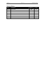
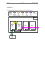
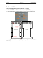
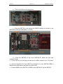
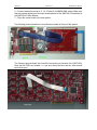
SMT8090_374
User Manual
User Manual (QCF42); Version 3.0, 8/11/00; © Sundance Multiprocessor Technology Ltd. 1999
Version 0.9
Page 2 of 12
SMT8090 User Manual
Revision History
Date
Comments
Engineer
Version
18/02/04
First release
PSR
0.9
25/06/04
Updates
PSR
1.0
Version 0.9
Page 3 of 12
SMT8090 User Manual
Table of Contents
Revision History............................................................................................................ 2
Table of Contents ......................................................................................................... 3
Contacting Sundance. .................................................................................................. 4
Notes............................................................................................................................. 4
Precautions................................................................................................................... 4
Outline description........................................................................................................ 5
Architecture................................................................................................................... 6
Hardware involved. ....................................................................................................... 7
Hardware installation. ................................................................................................... 8
Software applications. ................................................................................................ 11
3L application. ......................................................................................................... 11
Description of the functions in the test software menu........................................... 11
“Configuring FPGA
- Full configuration
- Loading keys and bitstream” ..... 11
“Configuring FPGA
- FPGA Already configured - Loading END key only” ..... 11
“Pulse on Config Line - for FPGA reconfiguring” ................................................ 11
“Configuring internal Registers” .......................................................................... 11
“Reading-back internal registers” ........................................................................ 11
“Temperature Updates” ....................................................................................... 12
“Serial Numbers Read Back” .............................................................................. 12
“Capturing data” .................................................................................................. 12
Pegasus application (to be done). .......................................................................... 12
Version 0.9
Page 4 of 12
SMT8090 User Manual
Contacting Sundance.
You can contact Sundance for additional information by sending email to
[email protected].
Notes.
-
SHB stands for Sundance High-speed Bus.
-
CommPort denotes an 8-bit communication port following the TI C4x
standards.
Precautions
In order to guarantee that Sundance’s boards function correctly and to protect the
module from damage, the following precautions should be taken:
-
They are static sensitive products and should be handled accordingly.
Always place the modules in a static protective bag during storage and
transition.
-
When operating, make sure that the heat generated by the system is
extracted e.g. a fan extracting heat or air blower. It is vital for the SMT390
daughter module.
Version 0.9
Page 5 of 12
SMT8090 User Manual
Outline description.
The SMT8090_374 is a dual-C6713 based module (SMT374) combined with a dual
high-speed ADC module (SMT390-VP composed of SMT338-VP and SMT390).
SMT374 characteristics:
⇒ Dual TMS320C6713 processor running at 225MHz
⇒ Six 20MB/s communication ports (comm.-ports)
⇒ 128MBytes of SDRAM (100MHz)
⇒ 8MByte Flash ROM for boot code and FPGA programming
⇒ Global expansion connector
⇒ General purpose I/O connector
⇒ High bandwidth data I/O via 2 Sundance High-speed Buses (SHB).
SMT390-VP characteristics:
⇒ Two 12-bit ADCs (AD9430-210) sampling at up to 210MHz via LVDS bus
(SLB),
⇒ Two Sundance High-speed Bus (SHB) connectors,
⇒ Two 4-channel Rocket Serial Link (RSL) connector – 2.5Gbits/second each,
⇒ Two 20 MegaByte/s communication ports,
⇒ Low-jitter on-board system clock,
⇒ Xilinx Virtex-II Pro FPGA (VP30-6),
⇒ 50-Ohm terminated analogue inputs and outputs, external triggers and
clocks via MMCX or MMBX(Huber and Suhner) connectors,
⇒ User defined pins for external connections,
⇒ Compatible with a wide range of Sundance SHB modules,
⇒ TIM standard compatible.
The SMT8090_374 is a demonstration software for the evaluation of the SMT374
and SMT390-VP modules. It can be used for prototyping 3G (3rd generation) systems
and high-speed data acquisition system with or without digital processor. This
document is an installation guide for the SMT8090_374 demonstration system.
The SMT8090_374 application gets the DSP on the SMT374 to configure the
SMT390_VP FPGA and control clock frequencies, clock routings, data format and
data capture. The DSP grabs data from both channels and stores them into a file for
further processing, like display and FFT.
Version 0.9
Page 6 of 12
SMT8090 User Manual
Architecture.
The following diagram shows the architecture of the SMT8090 system:
Analogue
Connection
Data
Global Bus
Connection
Data
SHB
Connection
Control
Comm
Port
Data
SDB
Connection
Data
Comm
Port
Processing
SMT310Q
SMT516
SMT374
DSP
SMT390
DAQ
Module #1
Module #2
Spare
Spare
MMCX to BNC cables
TIM site 1
PC
Host
TIM site 2
TIM site 3
TIM site 4
Version 0.9
Page 7 of 12
SMT8090 User Manual
Hardware involved.
The SMT8090_374 is built around two main modules but also involves a carrier
board and some cables to interconnect them and allow them to communicate with
each other and to access the PC.
⇒ 1x SMT310Q: PCI carrier
⇒ 1x SMT374: Dual-C6713 based module; to be plugged on site 1 of
SMT310Q.
⇒ 1x SMT390-VP: Dual-ADC module; to be plugged on site 2 of SMT310Q.
⇒ 1x FMS cable (20cm): to connect T1C0 to T2C3 at the back of the
SMT310Q.
⇒ 1x SMT516 (SHB to SHB PCB): to connect SHBA (SMT374) to SHBA
(SMT390).
⇒ 4x MMCX to BNC cables to connect an external analogue signal source to
J1 to J4 and an external clock source (when using external sampling clock) to J5 and
J6.
Version 0.9
Page 8 of 12
SMT8090 User Manual
Hardware installation.
Here are the steps to follow to install the SMT8090_374 system.
1 – Place the SMT374 on TIM site 1 of the carrier board (SMT310Q).
2 – The following are then required to mount SMT338-VP+390 on the SMT310Q:
Top Primary TIM Connector
Power
TIM 3.3V
Holes mounted with
Nylon screw (M2x10) and
4 Nylon nuts (M2)
RSL
B
RSL
A
SMT338-VP
SHB
B
SMT390
SHB
A
Holes mounted with
Nylon screw (M2x10) and
4 Nylon nuts (M2)
TIM 3.3V
Bottom Primary TIM Connector
a – First, fit two Nylon screws (M2x10), pointing out (the head of the screws on
bottom side).
Version 0.9
Page 9 of 12
SMT8090 User Manual
b – Then fit four M2 nuts on each screw.
c – Place the SMT338 on the second site (SMt374 already on first site) on the
SMT310Q and fit two metal pillars (3.3 Volts).
d – Place the SMT390 on top of the SMT338-VP. Make sure that both
modules fit firmly.
e – Fit two M2 nuts on the Nylon screws and two M3x4 screws in the 3.3V pillars.
3 – Connect CommPort 0 of the SMT374 to CommPort 3 of the SMT390 (T1C0 to
T2C3) via an FMS cable at the back of the SMT310Q.
4 – Connect SHBA on the SMT374 to SHBA on the SMT390-VP via the SMT516.
Version 0.9
Page 10 of 12
SMT8090 User Manual
5 – Connect external sources to J1, J4, J5 and J6 via MMCX-BNC cables. Make sure
that the external signal meet the input characteristics of the SMT390-VP described in
the SMT390-VP User Manual.
7 – Place the carrier board in the host system.
The following picture shows how connections are made at the top of the system:
The following picture shows the CommPort connection at the back of the SMT310Q.
Note that the FMS are ‘twisted’, i.e. one end should be blue and the other should
show silver pins.
Version 0.9
Page 11 of 12
SMT8090 User Manual
Software applications.
3L application.
In a sub-folder labelled 3L (directory SMT6600\Systems\SMT8090_374), you will find
a C (Test.c), a configuration (Test.cfg) and a make (nmake) files.
In a DOS prompt window, simply type nmake to generate the 3L application file,
which can be loaded into the SMT374 by using the 3L Server (3L Diamond needs to
be installed first).
This application allows the user to execute simple commands such as configuring the
ADC (output format and scale), the clock synthesizers, clock routing, capturing data,
etc.
Description of the functions in the test software menu.
The 3L application provided with the system allows the following option. Some will
prompt for a value. Before sending the control word to the SMT390. In some case
and where available, the internal control register is not only set up but also read-back
straight after to make sure it has been programmed properly. The value read-back is
displayed in the main window.
“Configuring FPGA
- Full configuration
- Loading keys and bitstream”
This command loads the bitstream contained in the directory where the application is
running from as well as the Start and End.
“Configuring FPGA
- FPGA Already configured - Loading END key only”
In the case where the FPGA has already been configured, by simply sending an End
Key, the FPGA retrieves it configuration. It saves time.
“Pulse on Config Line - for FPGA reconfiguring”
By toggling the Config line, it is possible to reload the FPGA with a different
bitstream.
“Configuring internal Registers”
Sets up the internal registers with values defines at the beginning of the application.
“Reading-back internal registers”
Reads-back all the registers (Clock selection, frequency, sample format, scale, etc)
that can be read-back.
Version 0.9
Page 12 of 12
SMT8090 User Manual
“Temperature Updates”
Once internal registers are configured, it is possible to read temperatures on the 338VP and 390.
“Serial Numbers Read Back”
Both modules SMT338-VP and SMT390 have a unique silicon serial number. This
function allows to read-then back and therefore identify the boards.
“Capturing data”
This command captures data from both channels, one after the other (not
simultaneously). Data are then stored into two separate files into the directory where
the application has been started. Files are called ChannelA.txt and ChannelB.txt
Pegasus application (to be done).
The SMT8090_374 is also provided with a Pegasus application (Pegasus folder),
which shows the user the dynamic performance of the system.