1
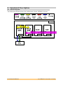
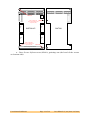
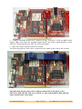
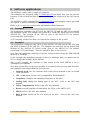
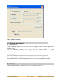
Sundance Multiprocessor Technology Limited
User Manual
Unit / Module Description:
What is this all about?
Unit / Module Number:
SMT8091
Form : QCF42
Date : 6 July 2006
Document Issue Number:
Issue Date:
Original Author:
Jean-Philippe Arnaud
User Manual
for
SMT8091
Sundance Multiprocessor Technology Ltd, Chiltern House,
Waterside, Chesham, Bucks. HP5 1PS.
This document is the property of Sundance and may not be copied
nor communicated to a third party without prior written
permission.
© Sundance Multiprocessor Technology Limited 2006
User Manual SMT8091
Last Edited: 15/09/2006 11:54:00
Revision History
Issue
1.0
Changes Made
First release
User Manual SMT8091
Page 2 of 16
Date
Initials
15/09/06
JPA
Last Edited: 15/09/2006 11:54:00
Table of Contents
1
Introduction ................................................................................................................... 5
2
Related Documents....................................................................................................... 7
2.1
Referenced Documents.............................................................................................. 7
2.2
Applicable Documents............................................................................................... 7
3
Acronyms, Abbreviations and Definitions ............................................................. 8
3.1
Acronyms and Abbreviations ................................................................................... 8
3.2
Definitions.................................................................................................................... 8
4
Functional Description ................................................................................................ 9
4.1
Block Diagram.............................................................................................................. 9
4.2
Hardware Description .............................................................................................. 10
5
Hardware installation.................................................................................................10
6
Software applications.................................................................................................14
6.1
Example0 .................................................................................................................... 14
6.2
Example1 .................................................................................................................... 14
6.3
Running the examples ............................................................................................. 15
6.4
Building the examples.............................................................................................. 15
7
Safety .............................................................................................................................15
8
EMC ................................................................................................................................16
User Manual SMT8091
Page 3 of 16
Last Edited: 15/09/2006 11:54:00
Table of Figures
Figure 1: GUI for example 0................................................................................................... 15
User Manual SMT8091
Page 4 of 16
Last Edited: 15/09/2006 11:54:00
1 Introduction
The SMT8091 is a single-C6416T based module (SMT395VP) combined with a dual
high-speed ADC module (SMT391-VP composed of SMT338-VP and SMT391).
SMT395VP characteristics:
⇒ Single TMS320C6416T processor running @ 1GHz (32 bits)
⇒ Six 20MB/s communication ports (comports)
⇒ Up to 256MBytes of SDRAM @ 133MHz
⇒ 8MByte Flash ROM for boot code and FPGA programming
⇒ Global expansion connector
⇒ General purpose I/O connector
⇒ High bandwidth data I/O via 2 Sundance High-speed Buses (32-bit SDB
interfaces)
⇒ 8 Rocket Serial links @ 2Gbit/s per lane for inter-module communications
SMT391-VP characteristics:
⇒ Dual 8-bit ADC (AT84AD001) sampling at up to 1Gsps via LVDS bus (SLB)
⇒ Two Sundance High-speed Bus (SHB) connectors
⇒ Two 4-channel Rocket Serial Link (RSL) connector – 2.5Gbit/s per lane
⇒ Two 20 MBytes/s communication ports (comport)
⇒ Low-jitter on-board system clock
⇒ Xilinx Virtex-II Pro FPGA (VP30-6)
⇒ 128MB DDR SDRAM
⇒ 50-Ohm terminated analogue inputs and outputs, external triggers and
clocks via MMCX or MMBX (Huber and Suhner) connectors
⇒ User defined pins for external connections
⇒ Compatible with a wide range of Sundance SHB modules
⇒ TIM standard compatible
User Manual SMT8091
Page 5 of 16
Last Edited: 15/09/2006 11:54:00
The SMT8091 is demonstration software for the evaluation of the SMT395VP and
SMT391-VP modules. It can be used for Broadband cable modem head-end systems,
Wireless infrastructure applications, 3G/4G Radio transceivers, Software Defined
Radio systems, Medical imaging systems, Spectrum analysers, High-speed data
acquisition system with or without digital processor. This document is an
installation guide for the SMT8091 demonstration system.
The SMT8091 application gets the DSP on the SMT395VP to configure the
SMT391_VP FPGA and control clock frequencies, clock routings, data format and
data capture. The DSP grabs data from both channels and stores them into a file for
further processing, like display and FFT.
User Manual SMT8091
Page 6 of 16
Last Edited: 15/09/2006 11:54:00
2 Related Documents
2.1 Referenced Documents
2.2 Applicable Documents
SMT395 user manual
SMT338-VP user manual
SMT391 user manual
User Manual SMT8091
Last Edited: 15/09/2006 11:54:00
3 Acronyms, Abbreviations and Definitions
3.1 Acronyms and Abbreviations
3.2 Definitions
User Manual SMT8091
Last Edited: 15/09/2006 11:54:00
4 Functional Description
4.1 Block Diagram
The following diagram shows the architecture of the SMT8091 system:
User Manual SMT8091
Last Edited: 15/09/2006 11:54:00
4.2 Hardware Description
The SMT8091 is built around two main modules but also involves a carrier board
and some cables to interconnect them and allow them to communicate with each
other and to access the PC.
⇒ 1x SMT310Q: PCI carrier
⇒ 1x SMT395VP: Single-C6416T based module; to be plugged on site 1 of
SMT310Q.
⇒ 1x SMT391-VP: Dual-ADC module; to be plugged on site 2 of SMT310Q.
⇒ 1x FMS cable (20cm): to connect T1C0 to T2C3 at the back of the
SMT310Q.
⇒ 1x SMT511 (SHB to SHB cable): to connect SHBB (SMT395VP) to SHBB
(SMT391VP).
⇒ 1x SMT516 (SHB to SHB PCB): to connect SHBA (SMT395VP) to SHBA
(SMT391VP).
⇒ 2x MMCX to BNC cables to connect an external analogue signal source to
J1 noted G (ChQ) and to J2 noted C (ChI).
5 Hardware installation
Here are the steps to follow to install the SMT8091 system.
1 – Place the SMT395VP on TIM site 1 of the carrier board (SMT310Q).
2 – The following are then required to mount SMT338-VP+391 on the SMT310Q:
User Manual SMT8091
Last Edited: 15/09/2006 11:54:00
Top Primary TIM Connector
Power
TIM 3.3V
Holes mounted with
Nylon screw (M2x10) and
4 Nylon nuts (M2)
RSL
B
RSL
A
SMT338-VP
SHB
B
SMT391
SHB
A
Holes mounted with
Nylon screw (M2x10) and
4 Nylon nuts (M2)
TIM 3.3V
Bottom Primary TIM Connector
a – First, fit two Nylon screws (M2x10), pointing out (the head of the screws
on bottom side).
User Manual SMT8091
Page 11 of 16
Last Edited: 15/09/2006 11:54:00
b – Then fit four M2 nuts on each screw.
c – Place the SMT338 on the second site (SMT395VP already on first site) on
the SMT310Q and fit two metal pillars (3.3 Volts).
d – Place the SMT391 on top of the SMT338-VP. Make sure that both modules
fit firmly.
e – Fit two M2 nuts on the Nylon screws and two M3x4 screws in the 3.3V
pillars.
3 – Connect Comport 1 of the SMT395VP to Comport 3 of the SMT391 (T1C0 to
T2C3) via an FMS cable at the back of the SMT310Q.
4 – Connect SHBA on the SMT395VP to SHBA on the SMT391-VP via the SMT516
(SHB to SHB PCB).
5 – Connect SHBB on the SMT395VP to SHBB on the SMT391-VP via the SMT511 (SHB
to SHB cable).
User Manual SMT8091
Page 12 of 16
Last Edited: 15/09/2006 11:54:00
6 – Connect external sources to J1 noted G (ChQ), J2 noted C (ChI) via MMCX-BNC
cables. Make sure that the external signal meets the input characteristics of the
SMT391-VP described in the SMT391-VP User Manual.
7 – Place the carrier board in the host system.
The following picture shows how connections are made at the top of the system:
The following picture shows the Comport connection at the back of the
SMT310Q. Note that the FMS are ‘twisted’, i.e. one end should be blue and the
other should show silver pins.
User Manual SMT8091
Page 13 of 16
Last Edited: 15/09/2006 11:54:00
6 Software applications
The SMT8091 comes with a couple of examples.
The examples are designed using 3L Diamond DSP and show how you can use the
features of the system and how to process the samples acquired by the ADC in the
DSP.
The SMT8091 is also supported by 3L Diamond FPGA and examples can be provided
on request to place processing in the FPGA.
Please refer to www.3L.com for more information about Diamond.
6.1 Example0
The application configures the FPGA of the SMT391-VP and the SMT391 to sample
the incoming signal. The samples are stored in a 16KB FIFO inside the FPGA of the
SMT338-VP. The content of the FIFO is sent to the SMT395-VP for further
processing (FFT) and display.
A GUI running on the host allows to control the settings of the system.
6.2 Example1
The application configures the FPGA of the SMT391-VP and sets up the ADC and
the clock generator of the SMT391. The samples are stored in the on-board DDR
SDRAM of the SMT338-VP before being sent to the SMT395-VP for further
processing ( FFT) and display. Data are stored in files on the host PC.
Note that the maximum sampling frequency allowed when using the DDR SDRAM
memory is 810Msps.
In the example the sampling frequency is fixed to 808Msps and you cannot use the
GUI to change the settings of the SMT391.
Also, in the example, the amount of data stored in the DDR SDRAM is set to
1Msamples per channel.
Note that writing files on the host machine is a relatively slow process and therefore
this example runs slower than the previous one.
•
External clock: use the external clock when ticked instead of the on-board
clock generator.
•
ChI -> ChQ: Input I of the ADC is sampled by both channels.
•
Frequency: configure the sampling frequency of the ADC.
•
Analog Gain: change the analog gain of the ADC.
manual
•
Offset Compensation: Refer to the ADC user manual
•
Reset: reset the pipeline of data inside the FPGA of the SMT338-VP
•
DRDA: refer to the ADC user manual
•
Built In Test: switch on the test mode of the ADC. refer to the ADC user
manual
User Manual SMT8091
Page 14 of 16
refer to the ADC user
Last Edited: 15/09/2006 11:54:00
Figure 1: GUI for example 0
6.3 Running the examples
3L Diamond users
For 3L Diamond version 3.1.5 or above, you can simply double click the .app file to
run the demo.
For 3L Diamond version 3.1.3, copy the file “clu3L_309.dll”
Windows/system32 folder prior to running the example.
in
your
6.4 Building the examples
This requires you have 3L Diamond version 3.1.3 or above installed.
Run the MAKEFILE provided in the example’s directory to compile the example.
7 Safety
This module presents no hazard to the user when in normal use.
User Manual SMT8091
Page 15 of 16
Last Edited: 15/09/2006 11:54:00
8 EMC
This module is designed to operate from within an enclosed host system, which is
build to provide EMC shielding. Operation within the EU EMC guidelines is not
guaranteed unless it is installed within an adequate host system.
This module is protected from damage by fast voltage transients originating from
outside the host system which may be introduced through the output cables.
Short circuiting any output to ground does not cause the host PC system to lock up
or reboot.
User Manual SMT8091
Last Edited: 15/09/2006 11:54:00