1
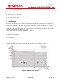
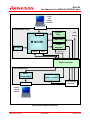
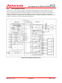
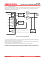
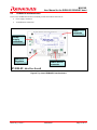
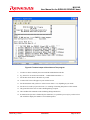
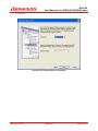
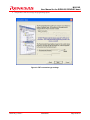
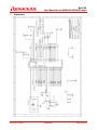
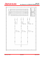
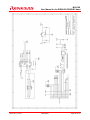
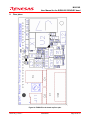
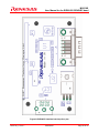
M16C/6S
User Manual for the EVB08-EU CENELEC band
M16C/6S
User Manual for the EVB08-EU CENELEC band
Abstract
This User Manual describes the usage and setup of the EVB08-EU evaluation board. The EVB08-EU is an evaluation
board for PLC communication within the CENELEC band. The EVB08-EU incorporates the Renesas M16C/6S
microcontroller including the YITRAN IT800 physical layer.
Target Device
Target device is the Renesas M16C/6S microcontroller, a member of the huge M16C microcontroller family.
Figure1: The EVB08-EU reference board
D007791_11 Rev.1
March2007
Page 1 of 1
M16C/6S
User Manual for the EVB08-EU CENELEC band
Contents
1.
Precautions for Safety....................................................................................................................... 3
2.
Content of EVB08-EU ....................................................................................................................... 7
3.
Introduction ....................................................................................................................................... 7
4. Hardware overview ........................................................................................................................... 8
4.1 EVB08-EU main board.................................................................................................................... 10
4.1.1
M16C/6S Microcontroller....................................................................................................... 11
4.1.2
Analog Front End .................................................................................................................. 12
4.1.3
EEPROM ............................................................................................................................... 13
4.1.4
24 pin Connector ................................................................................................................... 13
4.1.5
Miscellaneous Peripherals .................................................................................................... 14
4.2 EVB08-EU interface board.............................................................................................................. 15
4.2.1
Interface board 24 pin Connector.......................................................................................... 16
4.3 Power supply................................................................................................................................... 18
5. Software overview........................................................................................................................... 19
5.1 Minimum test software .................................................................................................................... 19
6. Getting started ................................................................................................................................ 20
6.1 Using the minimum Test Software .................................................................................................. 20
6.2 Flashing the M16C/6S .................................................................................................................... 22
6.2.1
Flashing with E8 and FDT ..................................................................................................... 22
6.3 Debugging the M16C/6S................................................................................................................. 27
7.
Schematics...................................................................................................................................... 28
8.
Floor plans ...................................................................................................................................... 33
9.
Abbreviations .................................................................................................................................. 36
10. References...................................................................................................................................... 37
Revision Record...................................................................................................................................... 38
D007791_11 Rev.1
March2007
Page 2 of 2
M16C/6S
User Manual for the EVB08-EU CENELEC band
1.
Precautions for Safety
Naturally, if you talk of power line communication you talk also about high voltages. Therefore you should be aware
about the risk of accidentally touching high voltages. Please handle this evaluation product with care, because it is not
protected against touching.
Warning
If the requirements shown in the
"WARNING" sentences are
ignored, the equipment may
cause serious personal injury or
death.
Caution
If the requirements shown in the
"CAUTION" sentences are
ignored, the equipment may
malfunction.
Important
It means important information
on using this product.
In addition to the three above, the following are also used as
appropriate.
means WARNING or CAUTION.
Example:
CAUTION AGAINST AN ELECTRIC SHOCK
means PROHIBITION
Example:
DISASSEMBLY PROHIBITED
means A FORCIBLE ACTION
Example:
UNPLUG THE POWER CABLE FROM THE
RECEPTACLE.
The following pages describe the symbols "WARNING", "CAUTION", and
"IMPORTANT".
D007791_11 Rev.1
March2007
Page 3 of 3
M16C/6S
User Manual for the EVB08-EU CENELEC band
Warnings for AC Power Supply:
• If the attached AC power cable does not fit the receptacle, do not alter the
AC power cable and do not plug it forcibly. Failure to comply may cause
electric shock and/or fire.
• When using outside Europe, use AC power cable which complies with the
safety standard of the country.
• When it is not possible to prepare for the AC power cable, contact your local
distributor.
• Do not touch the plug of the AC power cable when your hands are wet. This
may cause electric shock.
• This product is connected signal ground with frame ground. If your
developing product is transform less (not having isolation transformer of AC
power), this may cause electric shock. Also, this may give an unrepairable
damage to this product and your developing one. While developing, connect
AC power of the product to commercial power through isolation transformer in
order to avoid these dangers.
• If other equipment is connected to the same branch circuit care should be
taken not to overload the circuit. Refer to nameplate for electrical ratings.
• When installing this equipment, insure that a reliable ground connection is
maintained.
• If you smell a strange odor, hear an unusual sound, or see smoke coming
from this product, then disconnect power immediately by unplugging the AC
power cable from the outlet. Do not use this as it is because of the danger of
electric shock and/or fire. In this case, contact your local distributor.
Warnings to Be Taken for This Product:
• Do not disassemble or modify this product. Personal injury due to electric
shock may occur if this product is disassembled and modified.
• Make sure nothing falls onto the product, especially liquids, metal objects, or
anything combustible.
D007791_11 Rev.1
March2007
Page 4 of 4
M16C/6S
User Manual for the EVB08-EU CENELEC band
Warning for Installation:
• Do not set this product in water or areas of high humidity. Make sure that the
product does not get wet. Spilling water or some other liquid into the product
may cause unrepairable damage.
Warning for Use Environment:
• This equipment is to be used in an environment with a maximum ambient
temperature of 35°C. Care should be taken that this temperature is not
exceeded.
Cautions for AC Adapter:
• Use only the AC adapter included in this product package.
• The included AC adapter is for this product. Do not use it for other product.
• Before installing this equipment or connecting it to other equipment,
disconnect the AC power cable from its outlet to prevent injury or accident.
• The included AC adapter has not power supply switch. The AC adapter is
always active while connecting the AC power cable.
Cautions to Be Taken for This Product:
• Use caution when handling this product. Be careful not to apply a
mechanical shock.
• Do not touch the interface connector pins directly with your hand.
• Do not pull the product unit by the cable which is connected to this product.
Caution for AC Power Supply:
• When installing or connecting this product with other equipment, shut down
AC power or disconnect the AC power cord from the equipment to prevent
personal injury or damage to the equipment.
D007791_11 Rev.1
March2007
Page 5 of 5
M16C/6S
User Manual for the EVB08-EU CENELEC band
Caution for Installation:
• When in use do not replace the product from its side.
Caution for Communication Interface:
• Always make sure that the interface cable for communication to your host
application is matching.
Warnings for usage:
• Normal usage condition
In case the kit is used as a bundle as supplied with all components, the
external power supply supplies the needed voltages and the line coupler
functionality. So the main high voltage is not directly supplied to the EVB08EU main board, making the handling with the uncovered PCB safer.
• Usage under other conditions
In case the main board would be used as standalone PLC module and no
external line coupler exist, a line coupler can be assembled on the optional
pads provide on the PCB. In that case connect the high voltage AC230 to the
connector J11 the neutral phase to pin 1 and the L phase to pin 2. Please
make sure that your handling with high voltage is following the related
standards, because the main board is not protected against touching.
Warning concerning EMC Directive
• The EVB08-EU kit is only intended for use in a laboratory or classroom
environment. A safe separation distance of 20m should be used between this
and any sensitive equipment.
• Its use outside the laboratory, classroom, study area or similar such area
invalidates conformity with the protection requirements of the Electromagnetic
Compatibility Directive and could lead to prosecution.
D007791_11 Rev.1
March2007
Page 6 of 6
M16C/6S
User Manual for the EVB08-EU CENELEC band
2.
Content of EVB08-EU
The Renesas EVB08-EU consists of:
•
•
•
•
3.
1pcs EVB08-EU main board
1pcs EVB08-EU interface board
1pcs YITRAN IT800CA power supply
1pcs serial cross over cable
Introduction
Power line communication (PLC) is a method of communication using the existing electric power transmission and
electricity distribution lines in and outside home. The carrier can communicate data by superimposing an analogue
signal over the standard 50 or 60Hz main voltage frequency. Each room in a residence provides one, two, or more
outlets. These nodes are already available throughout the household, which makes PLC to a low-cost solution, by
offering this number of possible gateways. Any device requiring power is already attached to the power line network
making PLC convenient and accessible for every user.
The four major features for a successful communication solution are:
•
•
•
•
Ease to use
Ubiquitous node availability
Reliable
Cost effective
The Renesas M16C/6S PLC solution delivers all four.
In Europe the CENELEC standard EN50065-1 defines frequency bands for the data transmittion on low-voltage
electrical installations. These four bands are located in the frequency range from 3kHz to 148,5kHz.
Figure2: CENELEC band overview
D007791_11 Rev.1
March2007
Page 7 of 7
M16C/6S
User Manual for the EVB08-EU CENELEC band
Band
A
B
C
D
Frequency
Usage
3kHz - 95kHz
95kHz – 125kHz
125kHz – 140kHz
140kHz – 148,5kHz
Outdoor, reserved for energy suppliers
Indoor without access protocol
Indoor with access protocol
Indoor for alarm and security systems
Access
protocol
No
No
CSMA/CD
No
Table1:Usage of CENELEC band
In America and Japan other requirements for the signaling in that lower frequency bands exist.
Anyway, the Renesas M16C/6S PLC microcontroller does support the European CENELEC A and B band standard,
the American FCC standard and also the Japanese ARIB standard, by one chip. Only external component have to be
modified to adapt to the selected standard. With the Renesas M16C/6S PLC microcontroller, world wide customers can
be supported by only one platform.
4.
Hardware overview
In general the EVB08-EU kit consists of two PCBs:
• The upper main board
• Lower interface board.
Both PCBs are connected together by a 24 pin header connector.
Furthermore a socket power supply is provided with the kit package.
D007791_11 Rev.1
March2007
Page 8 of 8
M16C/6S
User Manual for the EVB08-EU CENELEC band
Flash
and
debug
Interface
14pin Connector
EVB08-EU Main board
Channel
filter
UART1
3,3V
Supply
Input filter
M16C/6S
Output
amplifier
EEPROM
UART0
AMP VCC
SIO3
24pin connector
PLC Interface board
RS232
Level shifter
5V
Voltage regulator
Power supply
connector
SUBD9
Terminal
Output
interface
Figure3: Block diagram of EVB08-EU
D007791_11 Rev.1
March2007
Page 9 of 9
M16C/6S
User Manual for the EVB08-EU CENELEC band
4.1
EVB08-EU main board
The heart of the four layer EVB08-EU main board PCB is the M16C/6S PLC microcontroller. Mounted around this
centre some external circuit of the Analogue Front End for the PLC physical layer, an EEPROM and a 14 pin connector
for flashing and debugging tasks are arranged. A 24 pin connector makes this board to a module, which can be plugged
easily to any application board.
LED
LED1 and LED2
Jumper
J5 and J6 and J8
Reset
M16C/6S
24pin J2
connector
Debug
and Flash
interface
Optional
pads for
line
coupler
Jumper J4
Optional pads for second Amplifier
Amplifier
Jumper J3
EVB08-EU main board
Figure4: Top view of EVB08-EU main board
24pin connector
EEPROM
EVB08-EU main board
Figure5: Bottom view of EVB08-EU main board
D007791_11 Rev.1
March2007
Page 10 of 10
M16C/6S
User Manual for the EVB08-EU CENELEC band
4.1.1
M16C/6S Microcontroller
The M16C/6S is a single chip microcomputer, built using the high-performance silicon gate CMOS process using a
M16C/60 Series CPU core and is packaged in a 64-pin plastic molded LQFP. These single-chip microcomputers
operate using sophisticated instructions featuring a high level of instruction efficiency, capable to execute instructions
at high speed. The M16C/6S is suitable for PLC networking, because it includes the advanced technology IT800
developed by YITRAN Corporations. With an embedded Flash memory of 96kByte and 24kBytes of RAM M16C/6S is
suitable even for larger protocol stacks and additional applications.
Figure6: Block diagram of M16C/6S chip
D007791_11 Rev.1
March2007
Page 11 of 11
M16C/6S
User Manual for the EVB08-EU CENELEC band
4.1.2
Analog Front End
The Analogue Front End (AFE) circuit includes reception and transmission paths and is located between Line Coupler
and M16C/6S. Some of the AFE circuits are on chip, some are external circuits. The following figure provides a
general description of the AFE block diagram.
M16C/6S
DAC
Output
Filter
Line
Driver
To line
coupler
Line
Driver
ADC
Channel
Filter
Input
Filter
Pre
Amp
Figure7: AFE General Block diagram
The on-chip AFE includes a Digital to Analogue Converter (DAC) in the transmission path, a pre-amplifier and an
Analogue to Digital Converter (ADC) in the reception path.
The DAC is part of the transmission path. This block is a current mode 10-Bit DAC which uses an internal current
reference to generate two complementary current outputs.
The external Input Filter is connected to the pre-amplifier, which is part of the reception path.
The output of each external channel filter in the reception path is connected to a 1-bit ADC input. There are three
similar ADC units incorporated in the chip. The ADC is built of an amplifier stage followed by a comparator stage.
D007791_11 Rev.1
March2007
Page 12 of 12
M16C/6S
User Manual for the EVB08-EU CENELEC band
4.1.3
EEPROM
The M16C/6S requires an external EEPROM (24Cxx serial EEPROM) connected by a two wire interface. The
EEPROM is used to store Dynamic Link Layer (DLL) parameters. The M16C/6S may also use the EEPROM to store
application data. A 128kBit version is mounted on the EVB08-EU board.
4.1.4
24 pin Connector
Usually the 24 pin connector will be used to plug the main board to the lower interface board supplied with this
package. Anyway, as mentioned before, it is also possible to use the main PCB as standalone module, therefore the
module has to be supplied with the below mentioned signals.
Please note that the main line signals at pin 22 and pin 24 are usually low voltage signals, because of the line coupler
inside of the socket power supply. In case the main board would be used as standalone PLC module and no external
line coupler exist, a line coupler can be assembled on the optional pads provided on the PCB. In that case pin 22 and
pin 24 should be connected to the high voltage 230V main lines. Please make sure that your handling with high voltage
is following the related standards, because the main board is not protected against touching.
Pin
1
2
3
4
5
6
7
8
9
10
11
12
13
14
15
16
17
18
19
20
21
22
23
24
Pin name
Description
P76 or P84
Not used (adjustable on Board)
P81
Not used
+3.3V
+3,3V digital supply voltage
GND
Digital ground
P74
Not used
RxD for RS232 (Convert to RS232-level by external circuit)
RxD0
TxD for RS232 (Convert to RS232-level by external circuit)
TxD0
CNVss
TA3OUT
GND
Digital ground
SPI data output (M16C/6S → Host)
MISO
SPI data ready output
BSNYC
NSS
SPI chip select (active low)
SPI data input (Host → M16C/6S)
MOSI
SPI Serial Clock
SPCK
+3.3V_AN
+3,3V analogue supply voltage
AMP VCC
amplifier supply voltage
GNDA
Analogue ground
RESET (active low)
RESET
P73
Not used
NC
Not connected
AC230VN_M Main neutral connection (only if line coupler is assembled on PCB)
NC
Not connected
AC230VL_M Main line connection (only if line coupler is assembled on PCB)
Table2: EVB08 Main Board 24 pin connector
D007791_11 Rev.1
March2007
Page 13 of 13
M16C/6S
User Manual for the EVB08-EU CENELEC band
4.1.5
Miscellaneous Peripherals
The EVB08-EU main board provides a few switches and jumpers to interact in the functionality of the board. Two
LEDs are assembled to PCB to indicate the current PLC communication status. Additionally a 14 pin Mil connector
interface for flashing and debugging of the M16C/6S is placed on top of the board.
J5
Description
1-2
P84 INT2 connect to J2
3-4
P/& TA3OUT connect to J2
Description
open
MCU in run mode
CNVSS pull down
shorted
LED1
Description
RED blinking
Sending data over PLC
J11
Connection
1
AC230VN
2
J6
AC230VL
LED2
Description
Receiving data over PLC
1-2
2-3
Description
CLK1 feed to J7
MCU in flash mode
CNVSS pull up
Green blinking
J3
J8
shorted
SW1
Description
pressed
RESET
J7
1
2
3
4
5
6
7
8
9
10
11
12
13
14
Description
VDCCN pull up normal
mode
VDCCN pull down test
mode
J4
Description
open
INT3 pull up
shorted
Deskription
P65 (SLCK)
Ground
CNVSS
N.C.
P67 (TXD1)
N.C.
P15(CE)
N.C.
P64(BUSY)
+3V3
P66(RXD1)
N.C.
RESETn
Ground
INT3 pull down
Figure8: Switches, jumpers, connectors and LEDs on the EVB08-EU main board
D007791_11 Rev.1
March2007
Page 14 of 14
M16C/6S
User Manual for the EVB08-EU CENELEC band
4.2
EVB08-EU interface board
The two layer EVB08-EU interface board PCB provides the needed connectors for:
•
Power supply connection
•
Terminal RS232 connection
24pin
connector
Power
supply
connector
AMP VCC
Regulator
SUBD9 RS232
connector
EVB08-EU interface board
Figure9: Top view of EVB08-EU interface board
D007791_11 Rev.1
March2007
Page 15 of 15
M16C/6S
User Manual for the EVB08-EU CENELEC band
4.2.1
Interface board 24 pin Connector
To connect it with the main board a 24 pin connector exists.
Pin
1
2
3
4
5
6
7
8
9
10
11
12
13
14
15
16
17
18
19
20
21
22
23
24
Pin name
Pull down
Pull down
+3.3V
GND
Pull down
RxD
TxD
EN1
CTS
RTS
Pull down
Pull down
Pull down
Pull down
Pull down
+3.3V_AN
AMP VCC
GNDA
RESET
Pull down
NC
AC230VN
NC
AC230VL
D007791_11 Rev.1
Description J4
+3,3V digital supply voltage
Digital ground
Not used
RxD for RS232 (Convert to RS232-level by external circuit)
TxD for RS232 (Convert to RS232-level by external circuit)
Enable for RS232
CTS for RS232
RTS for RS232
+3,3V analogue supply voltage
Amplifier supply voltage
Analogue ground
RESET (active low)
Not connected
Main neutral connection (only if line coupler is assembled on PCB)
Not connected
Main line connection (only if line coupler is assembled on PCB)
Table3: Interface Board 24 pin connector
March2007
Page 16 of 16
M16C/6S
User Manual for the EVB08-EU CENELEC band
J2
1-2
Description
For EVB04
jumper
AMP_VCC 12V
2-4
For EVB08
jumper
AMP_VCC 5V
AMP_VCC 5V
5-6
from external
power supply
jumper
J1
1
2
3
4
5
6
7
8
Pin name
GND
GND
+3.3V
+12V
+5V
AC230VL_M
AC230VN_M
nc
Ground signal
Ground signal
+3.3V power supply
+12V power supply
+5V power supply
Main line connection
Main line connection
J3
1
2
3
4
5
6
7
8
9
Pin name
nc
RxD
TxD
nc
GND
nc
RTS
CTS
nc
RxD at RS232 level
TxD at RS232 level
Ground signal
RTS at RS232 level
CTS at RS232 level
Figure10: Switches and connectors on the EVB08-EU interface board
D007791_11 Rev.1
March2007
Page 17 of 17
M16C/6S
User Manual for the EVB08-EU CENELEC band
4.3
Power supply
The AFE includes reception and transmission paths, with the required amplification. The line coupler couples the data
to the power line. In case of the EVB08-EU design the line coupler is included in the IT800CA power supply device
itself. Therefore, main voltage is not directly supplied to the EVB08-EU main board, making the handling with the
uncovered PCB safer.
Additional, the power supply includes a 12V, a 5V and a 3.3V regulation circuit, supplying the EVB08-EU board with
the required voltages.
Figure11: The YITRAN power supply including line coupler
D007791_11 Rev.1
March2007
Page 18 of 18
M16C/6S
User Manual for the EVB08-EU CENELEC band
5.
Software overview
The EVB08-EU will support different software options:
5.1
•
The standalone VB08-EU is pre-programmed with the minimum test software.
•
The EVB08-EU inside the PLC development kit is pre-programmed as RUN-M node, concentrator or sniffer.
Please refer to the RUN-M user manual for details.
Minimum test software
The low end test software does not include any protocol layer as well as no DLL. Error correction and other features
supported by the upper protocol layers are not included. This minimal test software is generating a menu via UART0
(connecter J3 of the interface board) at a HyperTerminal application running on a PC. The menu offers different
options to send test data from one node to another node. Therefore this software can be used excellently to test the
M16C/6S device.
Power supply
PC with
HyperTerminalTM
M16C/6S
AFE
and
Line coupler
Test Application
EEPROM
EVB08-EU
RS232 Interface
Figure12: M16C/6S system concept with minimum test software
D007791_11 Rev.1
March2007
Page 19 of 19
M16C/6S
User Manual for the EVB08-EU CENELEC band
6.
Getting started
Plug the EVB08-EU main board and the EVB08-EU interface board together. Connect the YITRAN power supply to
the lower interface board and connect it to a main line socket. To make sure the EVB08-EU bundle is working properly
you should press the reset button. The M16C/6S microcontroller on the EVB08-EU standalone version is already
flashed with suitable minimal test software by default. If you need other driver or protocol software please contact your
local Renesas sales office.
6.1
Using the minimum Test Software
The minimal test Software enables you to setup two nodes within your power line network. Depending on your
selection in a menu, one node will be the sender of information and the other one will be the receiver. The transmitting
node is sending a given number of data packets at a specific transfer speed and the receiving node is counting the
received number of packets. Before continuing, please make sure that the EVB08 board is configured as described in
the table below:
J8
J3
J6
J5
J4
shorted
1-2 shorted
open
Any position
Any position
Table3: Default setting for running test software
Now perform the following steps:
1.
Plug two EVB08-EU kits using the YITRAN power supply LSE0206CE into two separate wall
outlets.
2.
Connect the J3 SUBD9 connector to a PC COM port via a R232 cross over cable with a running
Terminal program as e.g. HyperTerminal.
3.
Please select following setting for the terminal software:
i. 19200 baud
ii. Data bits: 8
iii. Parity: none
iv. Stop bits: 1
v. Flow control: none
4.
Connect PC with running terminal software to the EVB08-EU kit node by serial cross over cable.
5.
Press the reset button
6.
Some information should appear on your PC terminal screen.
D007791_11 Rev.1
March2007
Page 20 of 20
M16C/6S
User Manual for the EVB08-EU CENELEC band
Figure14: Terminal output of the minimum Test program
7.
You have to choose manually the source node ID and destination node ID.
8.
E.g. choose for one node source node ID = 1 and destination node ID = 2.
9.
For the other node choose it the other way round.
10. A menu with 7 items will appear on your terminal screen.
11. For the transmitter node you have to select between items 1 to 6, depending on your needs.
12. For the receiver node you just select item 7, so counting of incoming data packets will be started.
13. The green LED of the receiver node is blinking during reception.
14. The red LED of the transmitter node is blinking during transmission.
15. If transmission of packets is finalized by the transmitter, it is possible to press any key on the receiver
side terminal to display the number of received data packets.
D007791_11 Rev.1
March2007
Page 21 of 21
M16C/6S
User Manual for the EVB08-EU CENELEC band
6.2
Flashing the M16C/6S
The EVB08-EU and the M16C/6S can be programmed with E8 and FDT3.07
6.2.1
Flashing with E8 and FDT
Please use the Flash development toolkit FDT version 3.07 or higher in combination with the E8 debugger.
You can download FDT at
http://eu.renesas.com/fmwk.jsp?cnt=flash_development_toolkit_tools_product_landing.jsp&fp=/products/tool
s/flash_prom_programming/fdt/
The hardware should be set into following status:
J8
J3
J6
J5
J4
Shorted
1-2 shorted
open
Any position
open
Table4: Default setting for synchronous flashing
Following steps should be taken for flash programming with E8:
1.
Connect the E8 to the EVB
2.
Open FDT Basic from your Renesas folder and select the device M306S0FA:
Figure15: FDT device selection
D007791_11 Rev.1
March2007
Page 22 of 22
M16C/6S
User Manual for the EVB08-EU CENELEC band
3.
select port E8:
Figure16: FDT communication port selection
D007791_11 Rev.1
March2007
Page 23 of 23
M16C/6S
User Manual for the EVB08-EU CENELEC band
4.
Keep default connection settings and programming options:
Figure16: FDT connection type settings
D007791_11 Rev.1
March2007
Page 24 of 24
M16C/6S
User Manual for the EVB08-EU CENELEC band
Figure17: FDT programming options
D007791_11 Rev.1
March2007
Page 25 of 25
M16C/6S
User Manual for the EVB08-EU CENELEC band
5.
Select
the checkbox ‘User / Data Area’
Figure18: FDT programming interface
6.
Select the mot-file to be flashed
7.
press ‘program flash’
8.
when the window ‘target power from E8’ appears press OK (E8 does not power the target)
D007791_11 Rev.1
March2007
Page 26 of 26
M16C/6S
User Manual for the EVB08-EU CENELEC band
6.3
Debugging the M16C/6S
For the debugging of the M16C/6S it is recommended to use:
•
The full M16C/62P emulation system PC7501 plus the additional signal converter board M306S0T-PRB in
cooperation with the PD30F debugger software (standalone integrated into HEW).
•
E8 debugger with the E8 debugger software (integrated into HEW)
The below steps describe the usage of the first debugging system only. Please note that in this case, the UART1 of the
M16C/6S cannot be used in your application software, if you like to debug the SW with KD30.
The hardware should be set into following status:
J8
J3
J6
J5
J4
shorted
1-2 shorted
open
Any position
open
Table7: Default setting for debugging of M16C/6S
For further information on how to use the E8 debugger in HEW please refer to the RUN-M user manual.
D007791_11 Rev.1
March2007
Page 27 of 27
M16C/6S
User Manual for the EVB08-EU CENELEC band
7.
Schematics
D007791_11 Rev.1
March2007
Page 28 of 28
M16C/6S
User Manual for the EVB08-EU CENELEC band
D007791_11 Rev.1
March2007
Page 29 of 29
M16C/6S
User Manual for the EVB08-EU CENELEC band
D007791_11 Rev.1
March2007
Page 30 of 30
M16C/6S
User Manual for the EVB08-EU CENELEC band
D007791_11 Rev.1
March2007
Page 31 of 31
M16C/6S
User Manual for the EVB08-EU CENELEC band
D007791_11 Rev.1
March2007
Page 32 of 32
M16C/6S
User Manual for the EVB08-EU CENELEC band
8.
Floor plans
Figure19: EVB08-EU main board top floor plan
D007791_11 Rev.1
March2007
Page 33 of 33
M16C/6S
User Manual for the EVB08-EU CENELEC band
Figure20: EVB08-EU main board bottom floor plan
D007791_11 Rev.1
March2007
Page 34 of 34
M16C/6S
User Manual for the EVB08-EU CENELEC band
Figure21: EVB08-EU interface board top floor plan
D007791_11 Rev.1
March2007
Page 35 of 35
M16C/6S
User Manual for the EVB08-EU CENELEC band
9.
Abbreviations
ADC (Analog to Digital Converter)
AFE (Analog Front End)
ARIB (Association of Radio Industries and Businesses)
CENELEC (European Committee for Electrotechnical Standardization)
DAC (Digital to Analog Converter)
DLL (Dynamic Link Layer)
FCC (Federal Communications Commission)
PLC (Power Line Communication)
D007791_11 Rev.1
March2007
Page 36 of 36
M16C/6S
User Manual for the EVB08-EU CENELEC band
10. References
Renesas Technology Corporation
http://www.renesas.com
Contact for Renesas Technical Support
E-mail: [email protected]
Data Sheet & User’s Manual
M16C/6S Datasheet, User’s Manual, other documents
(Use the latest version, please check: http://www.renesas.com)
YITRAN Communications Ltd.
http://www.yitran.com
Microsoft Corporation
http://www.microsoft.com
HyperTerminalTM
HyperTerminalTM is a trademark of Hilgrave Inc.
http://www.hilgraeve.com
CENELEC
EN50065-1; „Signaling on low-voltage electrical installations in the frequency range 3kHz to 148,5kHz“
D007791_11 Rev.1
March2007
Page 37 of 37
M16C/6S
User Manual for the EVB08-EU CENELEC band
Revision Record
Rev.
Rev.1A
Rev.1
Date
27.03.2007.
19.04.2007
D007791_11 Rev.1
Description
Section
all
all
Changed by
WRA
ASC
March2007
Summary
First edition issued
Initial version released
Page 38 of 38
M16C/6S
User Manual for the EVB08-EU CENELEC band
Keep safety first in your circuit designs!
1. Renesas Technology Corporation puts the maximum effort into making semiconductor products
better and more reliable, but there is always the possibility that trouble may occur with them. Trouble
with semiconductors may lead to personal injury, fire or property damage.
Remember to give due consideration to safety when making your circuit designs, with appropriate
measures such as (i) placement of substitutive, auxiliary circuits, (ii) use of nonflammable material or
(iii) prevention against any malfunction or mishap.
Notes regarding these materials
1. These materials are intended as a reference to assist our customers in the selection of the Renesas
Technology Corporation product best suited to the customer's application; they do not convey any
license under any intellectual property rights, or any other rights, belonging to Renesas Technology
Corporation or a third party.
2. Renesas Technology Corporation assumes no responsibility for any damage, or infringement of any
third-party's rights, originating in the use of any product data, diagrams, charts, programs,
algorithms, or circuit application examples contained in these materials.
3. All information contained in these materials, including product data, diagrams, charts, programs and
algorithms represents information on products at the time of publication of these materials, and are
subject to change by Renesas Technology Corporation without notice due to product improvements
or other reasons. It is therefore recommended that customers contact Renesas Technology
Corporation or an authorized Renesas Technology Corporation product distributor for the latest
product information before purchasing a product listed herein.
The information described here may contain technical inaccuracies or typographical errors.
Renesas Technology Corporation assumes no responsibility for any damage, liability, or other loss
rising from these inaccuracies or errors.
Please also pay attention to information published by Renesas Technology Corporation by various
means, including the Renesas Technology Corporation Semiconductor home page
(http://www.renesas.com).
4. When using any or all of the information contained in these materials, including product data,
diagrams, charts, programs, and algorithms, please be sure to evaluate all information as a total
system before making a final decision on the applicability of the information and products. Renesas
Technology Corporation assumes no responsibility for any damage, liability or other loss resulting
from the information contained herein.
5. Renesas Technology Corporation semiconductors are not designed or manufactured for use in a
device or system that is used under circumstances in which human life is potentially at stake.
Please contact Renesas Technology Corporation or an authorized Renesas Technology Corporation
product distributor when considering the use of a product contained herein for any specific
purposes, such as apparatus or systems for transportation, vehicular, medical, aerospace, nuclear,
or undersea repeater use.
6. The prior written approval of Renesas Technology Corporation is necessary to reprint or reproduce
in whole or in part these materials.
7. If these products or technologies are subject to the Japanese export control restrictions, they must
be exported under a license from the Japanese government and cannot be imported into a country
other than the approved destination.
Any diversion or reexport contrary to the export control laws and regulations of Japan and/or the
country of destination is prohibited.
8. Please contact Renesas Technology Corporation for further details on these materials or the
products contained therein.
D007791_11 Rev.1
March2007
Page 39 of 39