1
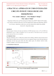
Lecture 5: Microwind/DCSH
CSCI 5330
Digital CMOS VLSI Design
Instructor: Saraju P. Mohanty, Ph. D.
NOTE: The figures, text etc included in slides are borrowed
from various books, websites, authors pages, and other
sources for academic purpose only. The instructor does
not claim any originality.
CSCE 5730: Digital CMOS VLSI Design
1
Lecture Outline
• Microwind Tool
• DCSH Tool
• Silicon Tool
Source:
1. http://www.microwind.org
2. Microwind Based Design (http://vsp2.ecs.umass.edu/vspg/658/
TA_Tools/microwind/Microwind.html)
CSCE 5730: Digital CMOS VLSI Design
2
Microwind and DSCH
• Microwind is a tool for designing and simulating circuits
at layout level. The tool features full editing facilities
(copy, cut, past, duplicate, move), various views (MOS
characteristics, 2D cross section, 3D process viewer),
and an analog simulator.
• DSCH is a software for logic design. Based on primitives,
a hierarchical circuit can be built and simulated. It also
includes delay and power consumption evaluation.
• Silicon is for 3D display of the atomic structure of silicon,
with emphasis on the silicon lattice, the dopants, and the
silicon dioxide.
CSCE 5730: Digital CMOS VLSI Design
3
Microwind and DSCH …
• Download
the
followings
http://www.microwind.org/
–Microwind3
–DSCH3
from
– User Manual: http://intrage.insatoulouse.fr/~etienne/microwind/manual_lite.pdf
• Installation and Use:
– Unzip the files above to be able to work with
Microwind.
– Read the reference manual for the software.
– Double click on Microwind3.exe to start the layout
editor or on Dsch3.exe to start the schematic editor.
CSCE 5730: Digital CMOS VLSI Design
4
Tools from Microwind
http://www.microwind.org/
•
•
•
•
•
•
•
•
Microwind
DSCH
Microwind3 Editor
Microwind 2D viewer
Microwind 3D viewer
Microwind analog simulator
Microwind tutorial on MOS devices
View of Silicon Atoms
CSCE 5730: Digital CMOS VLSI Design
5
Microwind and DSCH : NOR Example
• We will learn both the design flow and the CAD
tools.
• The specifications we are going to see may be
different for different foundry and technology.
• Design Example (3 Levels) : NOR Gate
– Logic Design
– Circuit Design
– Layout Design
CSCE 5730: Digital CMOS VLSI Design
6
Microwind / DSCH NOR Example: Logic
• Open the Schematic
Editor in Microwind
(DSCH3). Click on the
transistor symbol in the
Symbol Library on the
right.
• Instantiate NMOS or
PMOS transistors from
the symbol library and
place them in the editor
window.
CSCE 5730: Digital CMOS VLSI Design
7
Microwind / DSCH NOR Example: Logic
• Instantiate 2 NMOS and 2
PMOS transistors.
• Connect the drains and
sources of transistors.
CSCE 5730: Digital CMOS VLSI Design
8
Microwind / DSCH NOR Example: Logic
• Connect Vdd and GND
to the schematic.
• Connect input button and
output LED.
CSCE 5730: Digital CMOS VLSI Design
9
Microwind / DSCH NOR Example: Logic
• You now have NOR schematic
ready.
• Use your logic simulator to
verify the functionality of your
schematic.
• The next step is to simulate
the circuit and check for
functionality.
• Click on, Simulate -> Start
simulation.
• This brings up a Simulation
Control Window.
• Click on the input buttons to
set them to 1 or 0. Red color
in a switch indicates a '1'.
CSCE 5730: Digital CMOS VLSI Design
10
Microwind / DSCH NOR Example: Logic
• Inputs: 0 0
• Inputs: 0 1
CSCE 5730: Digital CMOS VLSI Design
11
Microwind / DSCH NOR Example: Logic
• Inputs: 1 0
• Inputs: 1 1
CSCE 5730: Digital CMOS VLSI Design
12
Microwind / DSCH NOR Example: Logic
• The simulation output can be observed as a waveform after the
application of the inputs as above. Click on the timing diagram icon in the
icon menu to see the timing diagram of the input and output waveforms.
CSCE 5730: Digital CMOS VLSI Design
13
Microwind / DSCH NOR Example: Circuit
• Simulate your system with
your
hand
calculated
transistor sizes.
• Click File -> Make Verilog
File.
The
Verilog,
Hierarchy
and
Netlist
window appears. This
window shows the verilog
representation of NOR
gate. Click OK to save the
Verilog as a .txt file.
CSCE 5730: Digital CMOS VLSI Design
14
Microwind / DSCH NOR Example: Circuit
• Open the layout editor
window
in
Microwind.
Click File -> Select
Foundry and select X.rul.
This sets your layout
designs in X technology.
• Click on Compile ->
Compile Verilog File. An
Open Window appears.
Select the .txt verilog file
saved before and open it.
CSCE 5730: Digital CMOS VLSI Design
15
Microwind / DSCH NOR Example: Circuit
• After selecting the .txt file,
a new window appears
called Verilog file.
• Click on Size on the right
top menus. This shows up
the NMOS and PMOS
sizes. Set the sizes
according to choice.
CSCE 5730: Digital CMOS VLSI Design
16
Microwind / DSCH NOR Example: Circuit
• Click Compile and then Back
to editor in the Verilog File
Window. This creates a
layout in layout editor
window using automatic
layout generation procedure.
• Add a capacitance to the
output of the design. The
value of the capacitance
depends on your choice.
CSCE 5730: Digital CMOS VLSI Design
17
Microwind / DSCH NOR Example: Circuit
• Click on OK. The
capacitance is shown on
the left bottom corner
with a value of 0.015fF.
• Click on the label marked In1. A
window appears. Click on the
Pulse option in the window. Insert
a 01 sequence for that specific
input and click on Insert. Then
click on Assign. Perform this
assignment on the other inputs.
CSCE 5730: Digital CMOS VLSI Design
18
Microwind / DSCH NOR Example: Circuit
• Click Simulate -> Run simulation. A simulation window appears with
inputs and output, shows the tphl, tplh and tp of the circuit. The power
consumption is also shown on the right bottom portion of the window.
• If you are unable to meet the specifications of the circuit change the
transistor sizes. Generate the layout again and run the simulations till
you achieve your target delays.
CSCE 5730: Digital CMOS VLSI Design
19
Microwind / DSCH NOR Example: Layout
• Design
the
layout
manually
• Open the layout editor
window in Microwind.
Click File -> Select
Foundry and select X.rul
• Vdd and GND rails are of
Metal1. The top rail is used
as Vdd and the bottom one
as GND. Click on Metal 1 in
the palette and then create
the required rectangle in the
layout window.
CSCE 5730: Digital CMOS VLSI Design
20
Microwind / DSCH NOR Example: Layout
• The next step is to build
the NMOS transistors.
Click on the transistor
symbol in the palette. Set
the W, L of the transistor.
• Then click on Generate
device. The source of the
transistor is connected to
the GND rail.
CSCE 5730: Digital CMOS VLSI Design
21
Microwind / DSCH NOR Example: Layout
• Create another NMOS and
place it in parallel to the first
NMOS device. We share the
two devices' drain diffusions. A
DRC check can be run by
clicking on Analysis -> Design
Rule Checker.
• The next step is to place
two PMOS transistors in
series.
CSCE 5730: Digital CMOS VLSI Design
22
Microwind / DSCH NOR Example: Layout
• Place the PMOs transistor on
layout close to the Vdd rail on the
top. To construct two PMOS
transistors in series, diffusions are
shifted to a side and another poly
line is added as second transistor.
The diffusion is shared to save
area and reduce capacitance.
• The next step is to
connect the inputs and the
output
of
the
two
transistors.
CSCE 5730: Digital CMOS VLSI Design
23
Microwind / DSCH NOR Example: Layout
• The next step is to connect
the poly to metal1 and then
• Poly inputs are connected
to metal2. The first symbol in
• Metal
output
is
the first row of the palette is
connected.
the poly to metal1 contact.
CSCE 5730: Digital CMOS VLSI Design
24
Microwind / DSCH NOR Example: Layout
• Then we connect the
metal1 to metal2 contact
to the previous contact.
This is the 4th contact on
the first row.
• The next step is to
connect
the
output
Metal1 to Metal2. Once
again use the 4th
contact in the first row.
CSCE 5730: Digital CMOS VLSI Design
25
Microwind / DSCH NOR Example: Layout
• Now we connect metal2 to the two inputs and one output
and bring them to the top to go out of the cell.
• Observe the two inputs (left & right) and an output (middle)
above the Vdd rail in dark blue color.
CSCE 5730: Digital CMOS VLSI Design
26
Microwind / DSCH NOR Example: Layout
• Now we label the inputs and output as In1, In2 and out.
Click on Add a Pulse Symbol in the palette (5th from the
right in the 3rd row). Then click on the metal2 of one of the
inputs. A window appears. Change the name of the input
signal. Insert a 01 sequences and click on Insert. The click
on Assign. Similarly assign the 2nd input a pulse.
CSCE 5730: Digital CMOS VLSI Design
27
Microwind / DSCH NOR Example: Layout
• Now select the Visible Node symbol from the palette (7th
in the third row). Select it and click on the output. The 'Add
a Visible Property' window appears. Change the label
name to out. Select Visible in Simulation. Click on Assign.
Now the output is also labeled.
CSCE 5730: Digital CMOS VLSI Design
28
Microwind / DSCH NOR Example: Layout
• Select Vdd Supply and GND from the
palette (third row). Also click on the
capacitor (3rd in 2nd row) symbol and
add it to the output. Also, extend the pwell into the Vdd Rail. The click on Edit
-> Generate -> Contacts. Select PATH
and then in Metal choose Metal1 and
N+ polarization.
• To run the Simulation of your
circuit, click on Simulate -> Start
Simulation. Depending on the input
sequences assigned at the input
the output is observed in the
simulation. The power value is also
given.
CSCE 5730: Digital CMOS VLSI Design
29
More Reading from Microwind Site
http://intrage.insa-toulouse.fr/~etienne/microwind/docs.html
• Introducing basic design rules. MOS design
rules, interconnect design rules, supply design
rules.
• Technology influence on design rules resistance
effect, capacitance effect, propagation.
• Specific design rules salicide, ldd, antenna ratio,
matching, supply rules, ESD.
• Introducing CMOS 90nm technology
• A very simple four-bit microprocessor designed
and simulated at gate level with DSCH3
CSCE 5730: Digital CMOS VLSI Design
30