1
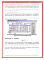
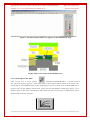
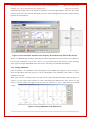
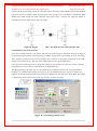
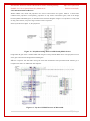
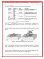
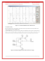
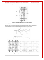
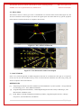
International Journal of Advance Research In Science And Engineering IJARSE, Vol. No.4, Special Issue (01), March 2015 http://www.ijarse.com ISSN-2319-8354(E) A PRACTICAL APPROACH OF CMOS INTEGRATED CIRCUITS WITH PC TOOLS DSCH2 AND MICROWIND 2 Prof. Ashish S. Bhaisare1, Prof. Madhuri P. Rodge 2, Prof. Anita S. Walde3 1 2 Department of Electronics and Telecommunication Engineering, SSJCET, Mumbai (M.S),( India) Asst. Professor and Head of Electronics and Telecommunication Engineering Department, SSJCET 3 Asst. Professor, Department of Electronics and Telecommunication Engineering, DIEMS, Dr.B.A.M.U. A'bad (M.S),( India) ABSTRACT The present paper introduces the design and simulation of CMOS integrated circuits, in PC tools DSCH and MICROWIND Version 2.6. Which will helpful for users not only analysis of VLSI subject but also research and practical approach from circuit to simulation. I. INTRODUCTION This paper summarized varies of MOS device structure device modeling, simulation at logic and layout levels which include the CMOS Inverter, the 2D and 3D views, the comparative design in micron and deep-submicron technologies, the basic logic gates (AND, OR, XOR, complex gates), the arithmetic functions (Adder, comparator, multiplier, ALU) also the latches and memories. 1.1 About Dsch (Version 2.6) Fig. 1 View of Cricuit simulator model in DSCH 890 | P a g e International Journal of Advance Research In Science And Engineering http://www.ijarse.com IJARSE, Vol. No.4, Special Issue (01), March 2015 ISSN-2319-8354(E) The DSCH program is a logic editor and simulator. DSCH is used to validate the architecture of the logic circuit before the microelectronics design is started. DSCH provides a user-friendly environment for hierarchical logic design, and fast simulation with delay analysis, which allows the design and validation of complex logic structures. DSCH also features the symbols, models and assembly support for 8051 and 18f64 microcontrollers. DSCH also includes an interface to WinSPICE. 1.2 About Microwind (Version 2.6) The MICROWIND program allows the student to design and simulate an integrated circuit at physical description level. The package contains a library of common logic and analog ICs to view and simulate. MICROWIND includes all the commands for a mask editor as well as original tools never gathered before in a single module (2D and 3D process view, Verilog compiler, tutorial on MOS devices). You can gain access to Circuit Simulation by pressing one single key. The electric extraction of your circuit is automatically performed and the analog simulator produces voltage and current curves immediately. Fig. 2 View of Cricuit Layout model in Microwind II. MOS LAYOUT IN MICROWIND We use MICROWIND to draw the MOS layout and simulate its behavior. Double-click on the MICROWIND icon. The MICROWIND display window includes four main windows: the main menu, the layout display window, the icon menu and the layer palette. The layout window features a grid, scaled in lambda () units. The lambda unit is fixed to half of the minimum available lithography of the technology. The default technology is a CMOS 8-metal layers 45 nm technology. In this technology, lambda is 0.02 μm (40 nm). The palette is located in the lower right corner of the screen. A red color indicates the current layer. Initially the selected layer in the palette is polysilicon. By using the procedure, we can create a manual design of the n-channel MOS. 891 | P a g e International Journal of Advance Research In Science And Engineering IJARSE, Vol. No.4, Special Issue (01), March 2015 http://www.ijarse.com ISSN-2319-8354(E) Figure 3- The Microwind window as it appears at the initialization stage Figure 4-The cross-section of the nMOS devices. 2.1 Vertical aspect of the MOS Click on this icon to access process simulation (Command Simulate Process section in 2D). The cross-section is given by a click of the mouse at the first point and the release of the mouse at the second point. In the example of Figure 4, three nodes appear in the cross-section of the n-channel MOS device: the gate (red), the left diffusion called source (green) and the right diffusion called drain (green), over a substrate (gray). A thin oxide called the gate oxide isolates the gate. Various steps of oxidation have lead to stacked oxides on the top of the gate. 892 | P a g e International Journal of Advance Research In Science And Engineering IJARSE, Vol. No.4, Special Issue (01), March 2015 http://www.ijarse.com ISSN-2319-8354(E) 2.2 Static Mos Characteristics Click on the MOS characteristics icon. The screen shown in Figure 2-5 appears. It represents the Id/Vd static characteristics of the nMOS device. The MOS size (width and length of the channel situated at the intersection of the polysilicon gate and the diffusion) has a strong influence on the value of the current. In Figure 2-5, the MOS width is 580 nm and the length is 40 nm. A high gate voltage (Vg = 1.0V) corresponds to the highest Id/Vd curve. For Vg=0, almost no current flows, Ids is close to 0. You may change the voltage values of Vd, Vg, Vs by using the voltage cursors situated on the right side of the window. Figure 5 : N-Channel Mos Characteristics 2.3 Dynamic MOS behavior The most convenient way to operate the MOS is to apply a clock to the gate, another to the source and to observe the drain. The summary of available properties that can be added to the layout is reported below. 2.3.1 Apply a clock to the gate. Click on the Clock icon and then, click on the polysilicon gate. Theclock menu appears again. Change the name into Vgate and click on OK to apply a clock with 0.1 ns period (45 ps at “0”, 5 ps rise, 45 ps at “1”, 5 ps fall). 2.3.2 Apply a clock to the drain. Click on the Clock icon, click on the left diffusion. The Clock menu appears. Change the name into Vdrain and click on OK. A default clock with 0.2 ns period is generated. The Clock property is sent to the node and appears at the right hand side of the desired location with the name Vdrain. 893 | P a g e International Journal of Advance Research In Science And Engineering IJARSE, Vol. No.4, Special Issue (01), March 2015 http://www.ijarse.com ISSN-2319-8354(E) 2.3.3 Watch the output: Click on the Visible icon and then, click on the right diffusion. Click OK. The Visible property is then sent to the node. The associated text s1 is in italic, meaning that the waveform of this node will appear at the next simulation Figure 6: The Clock Menu And The Clock Property Insertion Directly On The Mos Layout Always save BEFORE any simulation. The analog simulation algorithm may cause run-time errors leading to a loss of layout information. Click on File > Save as. A new window appears, into which you enter the design name. Type for example Mosn.MSK. Then click on Save. The design is saved under that filename 2.3.4 Analog Simulation Click on Simulate > start Simulation. The timing diagrams of the nMOS device appear, as shown in Figure 7 Select the appropriate time scale (500 ps) to see the chronograms of the simulation. Click “Reset” to restart simulation at any time. When vgate is at zero, no channel exists so the node vsource is disconnected from the drain. When the gate is on (vgate=1.0 V), the source copies the drain. It can be observed that the nMOS device drives well at zero but poorly at the high voltage. The highest value of vsource is around 0.6 V, that is VDD minus the threshold voltage. Figure 7: Analog simulation of the MOS device 894 | P a g e International Journal of Advance Research In Science And Engineering IJARSE, Vol. No.4, Special Issue (01), March 2015 http://www.ijarse.com ISSN-2319-8354(E) III. THE CMOS INVERTER First we can create CMOS Inverter circuit in DSCH software double clicking it located in the installed directory of dsch2 The following Screen will be appeared Figure 8: Main Window DSCH 3.1 Click on the pMOS and nMOS symbol button in the Symbol Library and drag it the schematic design areas as indicated in the figure. Figure 9: Simulating Schematic of CMOS Inverter in DSCH 895 | P a g e International Journal of Advance Research In Science And Engineering IJARSE, Vol. No.4, Special Issue (01), March 2015 http://www.ijarse.com ISSN-2319-8354(E) 3.2 The CMOS inverter design is detailed in the figure below. Here the p-channel MOS and the n-channel MOS transistors function as switches. When the input signal is logic 0 (Figure 10-a), the nMOS is switched off while PMOS passes VDD through the output. When the input signal is logic 1 (Figure 10-b right), the pMOS is switched off while the nMOS passes VSS to the output. Figure 10-aFigure 10-b : The MOS Inverter (File CmosInv.sch) 3.3 Manual Layout of the Inverter Click the icon MOS generator on the palette. The following window appears. By default the proposed length is the minimum length available in the technology (2 lambda), and the width is 10 lambda. In 45-nm technology, where lambda is 20 nm (0.02 µm), the corresponding size is 0.02 µm for the length and 0.04 µm for the width. Simply click Generate Device, and click on the middle of the screen to fix the MOS device. Click again the icon MOS generator on the palette. Change the type of device by a tick on p-channel, and click Generate Device. Click on the top of the nMOS to fix the pMOS device. The MOS generator is the safest way to create a MOS device compliant to design rules. The programmable parameters are the MOS width, length, the number of gates in parallel and the type of device (n-channel or pchannel). By default metal interconnects and contacts are added to the drain and source of the MOS. We can add a supplementary metal 2 interconnect on the top of metal 1 for drain and source. Figure 11 : Generating a nMOS device 896 | P a g e International Journal of Advance Research In Science And Engineering IJARSE, Vol. No.4, Special Issue (01), March 2015 http://www.ijarse.com ISSN-2319-8354(E) 3.4 Connection between Devices Within CMOS cells, metal and polysilicon are used as interconnects for signals. Metal is a much better conductor than polysilicon. Consequently, polysilicon is only used to interconnect gates, such as the bridge between pMOS and nMOS gates, as described in the schematic diagram of figure 13. Polysilicon is rarely used for long interconnects, except if a huge resistance value is expected. In the layout shown in figure 13, the polysilicon Figure 13 : Polysilicon bridge between nMOS and pMOS devices bridge links the gate of the n-channel MOS with the gate of the p-channel MOS device. The polysilicon serves as the gate control and the bridge between MOS gates. 3.5 Save respective file and make verilog file with same destination and Open Microwind software go to Compile with same row width limit and compile it. Figure 14: Layout of CMOS Inverter in Microwind 897 | P a g e International Journal of Advance Research In Science And Engineering http://www.ijarse.com IJARSE, Vol. No.4, Special Issue (01), March 2015 ISSN-2319-8354(E) 3.6 Useful Editing Tools The following commands may help you in the layout design and verification processes. Figure 15 : A set of useful editing tools 3.7 Process steps to build the Inverter At that point, it might be interesting to illustrate the steps of fabrication as they would sequence in a foundry. MICROWIND includes a 3D process viewer for that purpose. Click Simulate →Process steps in 3D. The simulation of the CMOS fabrication process is performed, step by step by a click on Next Step. On figure 313, the picture on the left represents the nMOS device, pMOS device, common polysilicon gate and contacts. The picture on the right represents the same portion of layout with the metal layers stacked on top of the active devices. Figure 16 : The step-by-step fabrication of the Inverter circuit 3.6 The command Simulate →Run Simulation gives access to the analog simulation. Select the simulation mode Voltage vs. Time. The analog simulation of the circuit is performed. The time domain waveform, proposed by default, details the evolution of the voltages in1 and out1 versus time. This mode is also called transient simulation, as shown in figure 17 The truth-table is verified as follows. A logic “0” corresponds to 0 V a logic “1” to a 1. 0 V. When the input rises to “1”, the output falls to “0”, with a 7 pico-second delay (7.10-12 second). The reason why the delay is larger before time 1.0 ns is that the circuit is “warming up” as the voltage supply suddenly rises from 0 to VDD at time= 0.0ns. The steady-state is reached at time=1.0 ns. 898 | P a g e International Journal of Advance Research In Science And Engineering IJARSE, Vol. No.4, Special Issue (01), March 2015 http://www.ijarse.com ISSN-2319-8354(E) F i Figure 17 : Transient simulation of the CMOS inverter IV. BASIC GATES Here are some basic gates circuit diagram in dsch software and its layout in Microwind. The procedure all are same as explain above steps in CMOS inverter 4.1 The Nand Gate: The truth-table and logic symbol of the NAND gate with 2 inputs are shown below.In DSCH , select the NAND symbol in the palette, add two buttons and one lamp as shown above. Add interconnects if necessary to link the button and lamps to the cell pins. Verify the logic behaviour of the cell. Figure 18: Schematic Diagram of the CMOS NAND Gate Design 899 | P a g e International Journal of Advance Research In Science And Engineering IJARSE, Vol. No.4, Special Issue (01), March 2015 http://www.ijarse.com ISSN-2319-8354(E) Figure 19 : A NAND cell created by the CMOS compiler. 4.2 The XOR Gate There exist many possibilities for implementing the XOR function into CMOS. The least efficient design, but the most forward, consists in building the XOR logic circuit from its Boolean equation. Figure 20 : The schematic diagram of the XOR gate Figure 21 : Layout and simulation of the XOR gate 900 | P a g e International Journal of Advance Research In Science And Engineering IJARSE, Vol. No.4, Special Issue (01), March 2015 http://www.ijarse.com ISSN-2319-8354(E) 4.3 Silicon Menu The software “silicon” is able to give a user’s controlled 3D view of silicon atoms such as SiO2 (figure 22). The 3D view of the lattice shown in figure 12-2 shows the regular aspect of Si atoms and the very specific properties of the material. One boron atom acts as a dopant in the structure. Figure 22 : The « silicon » main menu Figure 23 : The silicon lattice and a boron dopant V. CONCLUSIONS Since it is a practical approach of CMOS integrated circuit but its not limited for cmos gate or its respective circuit. We can use dsch and Microwind pc tools for microcontroller simulation and with using verilog file which is compile in microwind software. REFERENCES [1] “Chip Design for Submicron VLSI: CMOS Layout and Simulation” by John Uyemura - Georgia Institute of Technology, USA - 2005, IBSN 053446629X. [2] Sung-Mo Kang and Yusuf Leblebici, “CMOS Digital Integrated Circuits Analysis and Design”, Tata McGraw Hill, 3rd Edition, 2012. [3] Jan M. Rabaey, Anantha Chandrakasan and Borivoje Nikolic, “Digital Integrated Circuits: A Design Perspective”, Pearson Education, 2nd Edition. 901 | P a g e International Journal of Advance Research In Science And Engineering IJARSE, Vol. No.4, Special Issue (01), March 2015 [4] http://www.ijarse.com ISSN-2319-8354(E) Microwind & Dsch Version 3.5 User's Manual Lite Version September 2009 by Etienne Sicard WEB INFORMATION [1] www.microwind.org for general information about MICROWIND [2] www.microwind.net to download the lite version and order the professional version ABOUT AUTHORS 1) Prof. Ashish S. Bhaisare Is Assistant professor in Electronics and Telecommunication Engineering Department at Shivajirao S. Jondhle college of Engineering and Technology, Asangaon, Mumbai since five years. He completed B.E (Electronics) in 2009 from Mumbai University and M.E (Digital Electronics) from North Maharashtra University. His area of research work in Analog Electronics, VLSI Design, Integrated circuit and satellite communication. He is lifetime member of IETE and UACEE. 2) Prof. Madhuri P Rodge Is Associate professor and Head of Department in Electronics and Telecommunication Engineering at Shivajirao S. Jondhle college of Engineering and Technology, Asangaon, Mumbai also she is lifetime member of IETE having 16 year of academic teaching experience, her area of expertization work in microprocessors. Presently doing Ph.D in Mobile Communication. 3) Prof. Anita S. Walde Is Assistant professor in Electronics and Telecommunication Department at Deogiri Institute of Engineering and Management Studies,Aurngabad. She has 14 years of academic teaching experience, her area of expertization work in singal processing and control sysytems. Presently doing Ph.D in Electronics at Dr.B.A.M.U. Aurngabad (M.S) 902 | P a g e