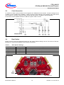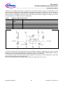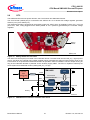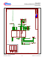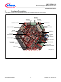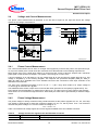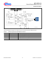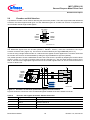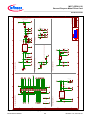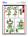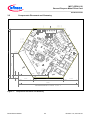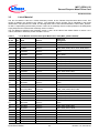
1
XMC4400 Motor Control Application Kit Part Number: KIT_XMC44_AE3_001 How long does it take to get a motor turn? Few minutes with the XMC4400 Motor Control Application Kit. It has everything you need to make a plug&play experience for 3 –Phase drives. This kit has a XMC4400 Microcontroller Board, the respective 24V power board including N-Channel Optimos™ power transistors and 3 phase gate driver EiceDRIVER™ from Infineon, completed with a brushless DC motor. It’s supported by the DAVE™ Motor Control Apps library, including sinusoidal and block commutation as well as various position detection and sensing schemes with encoder, resolver, hall sensors and shunts. Features XMC4400 Microcontroller Board Power board: - - 24V/7.5 A 3-Phase Inverter with N-Channel Optimos™ power transistors (BSC031N06NS3 G) and EiceDRIVER™ gate driver (6ED003L02-F2) 3-Phase Inverter by Reverse Conduction IGBT PLEASE SEE THE FOLLOWING PAGES FOR THE USERS MANUAL: User manuals included below: - Board User's Manual "CPU Board XMC4400 General Purpose" - Board User's Manual "General Purpose Motor Drive Card" He xa gon Applic atio n Ki t For XMC4000 Family CP U_ 44 A - V2 CPU Board XMC4400 General Purpose Boa rd Us er‘s Ma nu al Revision 1.0, 2013-02-19 Mic rocon t rolle r Edition 2013-02-19 Published by Infineon Technologies AG 81726 Munich, Germany © 2013 Infineon Technologies AG All Rights Reserved. Legal Disclaimer The information given in this document shall in no event be regarded as a guarantee of conditions or characteristics. With respect to any examples or hints given herein, any typical values stated herein and/or any information regarding the application of the device, Infineon Technologies hereby disclaims any and all warranties and liabilities of any kind, including without limitation, warranties of non-infringement of intellectual property rights of any third party. Information For further information on technology, delivery terms and conditions and prices, please contact the nearest Infineon Technologies Office (www.infineon.com). Warnings Due to technical requirements, components may contain dangerous substances. For information on the types in question, please contact the nearest Infineon Technologies Office. Infineon Technologies components may be used in life-support devices or systems only with the express written approval of Infineon Technologies, if a failure of such components can reasonably be expected to cause the failure of that life-support device or system or to affect the safety or effectiveness of that device or system. Life support devices or systems are intended to be implanted in the human body or to support and/or maintain and sustain and/or protect human life. If they fail, it is reasonable to assume that the health of the user or other persons may be endangered. CPU_44A-V2 CPU Board XMC4400 General Purpose Revision History Page or Item Subjects (major changes since previous revision) Revision 1.0, 2013-02-19 Initial release Trademarks of Infineon Technologies AG AURIX™, C166™, CanPAK™, CIPOS™, CIPURSE™, EconoPACK™, CoolMOS™, CoolSET™, CORECONTROL™, CROSSAVE™, DAVE™, EasyPIM™, EconoBRIDGE™, EconoDUAL™, EconoPIM™, EiceDRIVER™, eupec™, FCOS™, HITFET™, HybridPACK™, I²RF™, ISOFACE™, IsoPACK™, MIPAQ™, ModSTACK™, my-d™, NovalithIC™, OptiMOS™, ORIGA™, PRIMARION™, PrimePACK™, PrimeSTACK™, PRO-SIL™, PROFET™, RASIC™, ReverSave™, SatRIC™, SIEGET™, SINDRION™, SIPMOS™, SmartLEWIS™, SOLID FLASH™, TEMPFET™, thinQ!™, TRENCHSTOP™, TriCore™. Other Trademarks Advance Design System™ (ADS) of Agilent Technologies, AMBA™, ARM™, MULTI-ICE™, KEIL™, PRIMECELL™, REALVIEW™, THUMB™, µVision™ of ARM Limited, UK. AUTOSAR™ is licensed by AUTOSAR development partnership. Bluetooth™ of Bluetooth SIG Inc. CAT-iq™ of DECT Forum. COLOSSUS™, FirstGPS™ of Trimble Navigation Ltd. EMV™ of EMVCo, LLC (Visa Holdings Inc.). EPCOS™ of Epcos AG. FLEXGO™ of Microsoft Corporation. FlexRay™ is licensed by FlexRay Consortium. HYPERTERMINAL™ of Hilgraeve Incorporated. IEC™ of Commission Electrotechnique Internationale. IrDA™ of Infrared Data Association Corporation. ISO™ of INTERNATIONAL ORGANIZATION FOR STANDARDIZATION. MATLAB™ of MathWorks, Inc. MAXIM™ of Maxim Integrated Products, Inc. MICROTEC™, NUCLEUS™ of Mentor Graphics Corporation. Mifare™ of NXP. MIPI™ of MIPI Alliance, Inc. MIPS™ of MIPS Technologies, Inc., USA. muRata™ of MURATA MANUFACTURING CO., MICROWAVE OFFICE™ (MWO) of Applied Wave Research Inc., OmniVision™ of OmniVision Technologies, Inc. Openwave™ Openwave Systems Inc. RED HAT™ Red Hat, Inc. RFMD™ RF Micro Devices, Inc. SIRIUS™ of Sirius Satellite Radio Inc. SOLARIS™ of Sun Microsystems, Inc. SPANSION™ of Spansion LLC Ltd. Symbian™ of Symbian Software Limited. TAIYO YUDEN™ of Taiyo Yuden Co. TEAKLITE™ of CEVA, Inc. TEKTRONIX™ of Tektronix Inc. TOKO™ of TOKO KABUSHIKI KAISHA TA. UNIX™ of X/Open Company Limited. VERILOG™, PALLADIUM™ of Cadence Design Systems, Inc. VLYNQ™ of Texas Instruments Incorporated. VXWORKS™, WIND RIVER™ of WIND RIVER SYSTEMS, INC. ZETEX™ of Diodes Zetex Limited. Last Trademarks Update 2011-02-24 Template: IFX_Template_2011-02-24.dot CPU_44A-V2 CPU Board XMC4400 General Purpose Table of Contents Table of Contents Introduction ............................................................................................................................................................ 7 1 1.1 1.2 Overview ............................................................................................................................................. 7 Key Features ........................................................................................................................................ 7 Block Diagram ...................................................................................................................................... 8 2 2.1 2.2 2.3 2.4 2.5 2.5.1 2.5.2 2.5.3 2.6 2.7 2.8 2.9 2.10 2.11 2.11.1 2.11.2 2.11.3 Hardware Description ........................................................................................................................ 9 Power Supply ....................................................................................................................................... 9 Reset .................................................................................................................................................. 12 Clock Generation................................................................................................................................ 13 Boot Option ........................................................................................................................................ 13 Debug Interface .................................................................................................................................. 14 On-board USB Debugger ................................................................................................................... 15 Cortex Debug Connector (10-pin) ...................................................................................................... 16 Cortex Debug+ETM Connector (20-pin) ............................................................................................ 17 RGB LED ............................................................................................................................................ 19 USB .................................................................................................................................................... 19 RTC .................................................................................................................................................... 21 User LEDs and User Buttons ............................................................................................................. 22 Potentiometer ..................................................................................................................................... 22 Satellite Connectors ........................................................................................................................... 23 COM Connector ................................................................................................................................. 24 HMI Connector ................................................................................................................................... 25 ACT Satellite Connector ..................................................................................................................... 26 3 3.1 3.2 3.3 Production Data................................................................................................................................ 26 Schematics ......................................................................................................................................... 26 Component Placement and Geometry ............................................................................................... 31 Bill of Material (BOM) ......................................................................................................................... 32 Board User's Manual 4 Revision 1.0, 2013-02-19 CPU_44A-V2 CPU Board XMC4400 General Purpose List of Figures List of Figures Figure 1 Figure 2 Figure 3 Figure 4 Figure 5 Figure 6 Figure 7 Figure 8 Figure 9 Figure 10 Figure 11 Figure 12 Figure 13 Figure 14 Figure 15 Figure 16 Figure 17 Figure 18 Figure 19 Figure 20 Figure 21 Figure 22 Figure 23 Figure 24 Figure 25 Figure 26 Figure 27 Figure 28 Figure 29 CPU_44A-V2 Board Block Diagram..................................................................................................... 8 CPU Board XMC4400 General Purpose (CPU_44A-V2)..................................................................... 9 Powering Option ................................................................................................................................. 10 Block Diagram Of Power Supply ........................................................................................................ 10 Reset Circuit ....................................................................................................................................... 12 Reset LED and Reset Button ............................................................................................................. 12 Clock Generation................................................................................................................................ 13 Boot Options Switch ........................................................................................................................... 13 Installation of Serial Port Driver .......................................................................................................... 15 On-Board USB Debugger .................................................................................................................. 15 Cortex Debug Connector (10-pin) ...................................................................................................... 16 Cortex Debug Connector (10-pin) Layout .......................................................................................... 16 Cortex Debug+ETM Connector (20-pin) ............................................................................................ 17 Cortex Debug+ETM Connector (20-pin) Layout ................................................................................ 18 RGB LED ............................................................................................................................................ 19 USB Connector .................................................................................................................................. 19 USB power generation - Host/OTG mode ......................................................................................... 20 Battery Holder for Coin Cells .............................................................................................................. 21 XMC4400 Power Domains and Real Time Clock .............................................................................. 21 User LEDs and User Buttons ............................................................................................................. 22 Satellite Connectors ........................................................................................................................... 23 Satellite Connector Type COM .......................................................................................................... 24 Satellite Connector Type HMI ............................................................................................................ 25 Satellite Connector Type ACT ............................................................................................................ 26 Satellite Connectors, USB-OTG......................................................................................................... 27 XMC4400 ........................................................................................................................................... 28 Power, Debug Connectors, Reset...................................................................................................... 29 On-board Debugger ........................................................................................................................... 30 Component Placement and Geometry ............................................................................................... 31 Board User's Manual 5 Revision 1.0, 2013-02-19 CPU_44A-V2 CPU Board XMC4400 General Purpose List of Figures List of Tables Table 1 Table 2 Table 3 Table 4 Table 5 Table 6 Table 7 Table 8 Table 9 Table 10 Table 11 Power status LED’s ............................................................................................................................ 10 Power Measurement .......................................................................................................................... 11 Boot Options Settings ........................................................................................................................ 13 Cortex Debug Connector (10 Pin) ...................................................................................................... 16 Cortex Debug+ETM Connector (20 Pin) ............................................................................................ 17 RGB LED Connections ...................................................................................................................... 19 USB micro AB connector Pinot .......................................................................................................... 20 User LEDs .......................................................................................................................................... 22 User Buttons ....................................................................................................................................... 22 Potentiometer ..................................................................................................................................... 22 BOM of CPU_44A-V2 Board .............................................................................................................. 32 Board User's Manual 6 Revision 1.0, 2013-02-19 CPU_44A-V2 CPU Board XMC4400 General Purpose Overview Introduction This document describes the features and hardware details of the CPU Board XMC4400 General Purpose (CPU_44A-V2) designed to work with Infineon’s XMC4400 Microcontroller. This board is part of Infineon’s Hexagon Application Kits. 1 Overview The CPU board CPU_44A-V2 houses the XMC4400 Microcontroller and three satellite connectors (HMI, COM, ACT) for application expansion. The board along with satellite cards (e.g. HMI_OLED-V1, COM_ETH-V1, AUT_ISO-V1 boards) demonstrates the capabilities of the XMC4400. The main use case for this board is to demonstrate the generic features of the XMC4400 device including tool chain. The focus is safe operation under evaluation conditions. The board is neither cost nor size optimized and does not serve as a reference design. 1.1 Key Features The CPU_44A-V2 board is equipped with the following features ® XMC4400 (ARM Cortex™-M4-based) Microcontroller, 512 kByte on-chip Flash, LQFP-100 Connection to satellite cards via the satellite connectors COM, HMI and ACT USB OTG Host/Device support via micro USB connector Debug options − On-board Debugger via the Debug USB connector − Cortex Debug connector 10-pin (0.05”) − Cortex Debug+ETM connector 20-pin (0.05”) Reset push button RGB LED connected to GPIOs P1.10, P1.11 and P5.7 Boot option switch PowerScale Connector: Ready for power consumption analysis 7 LED’s − 3 Power indicating LEDs − 2 User LEDs (P5.2 and P1.8) − 1 RESET LED − 1 Debug LED Two User Buttons connected to HIB_IO_0 and P0.10 Potentiometer, connected to analog input P14.1 Power supply − Via Micro-USB connector in USB device mode − Via satellite connector pins (COM/ACT satellites cards can supply power to CPU board) − Via Debug USB connector − RTC backup battery Board User's Manual 7 Revision 1.0, 2013-02-19 CPU_44A-V2 CPU Board XMC4400 General Purpose Overview 1.2 Block Diagram Figure 1 shows the functional block diagram of the CPU_44A-V2 board. For more information about the power supply please refer to chapter 2.1. The CPU board has got the following building blocks: 3 Satellite Connectors (COM, HMI ACT) 2 User LEDs connected to GPIOs P5.2 and P1.8 2 User Buttons connected to HIB_IO_0 and P0.10 RGB LED connected to GPIOs P1.10, P1.11 and P5.7 2 Cortex Debug Connectors Variable resistor (POTI) connected to GPIO P14.1 USB On-The-Go Connector (Micro-USB) On-board Debugger via Debug USB connector (Micro-USB) Debug 10pin Debug 20pin On-board Debugger XMC4200 SWV SWD SWV SWD UART Debug USB USB OTG 2xLED CAN JTAG UART CPU Board XMC4400 General Purpose 2xButton CPU_44A-V2 USB GPIO U0C0 RS485 XMC4400 LQFP100 EXTBUS ETH ETH CAN CAN1 EE U0C1 3xCS CCU81 U1C0 QSPI CAPCOM POSIF ENCODER DSD DSMOD DAC OPAMP ADC SENSOR POTI RGB LED SPI SPI 2xISOFACE 4xGPIO GPIO I2C SPI GPIO GPIO I2C_IOEX ACT COM CAN RMII CCU 4/8 I2C I2C I2C_IOEX HMI I2C_IOEX reset OLED HEADSET cmd SDCARD TOUCH Figure 1 Block_Diag.emf CPU_44A-V2 Board Block Diagram Board User's Manual 8 Revision 1.0, 2013-02-19 CPU_44A-V2 CPU Board XMC4400 General Purpose Hardware Description 2 Hardware Description The following sections give a detailed description of the hardware and how it can be used. USB OTG Connector Debug USB Connector ACT Satellite Connector COM Satellite Connector On-board Debugger User LEDs and User Buttons RGB LED Power indicating LEDs Boot Option Switch XMC4400 CPU Reset Circuit Debug Connectors Battery Holder Potentiometer HMI Satellite Connector Figure 2 2.1 Board_Interfaces.emf CPU Board XMC4400 General Purpose (CPU_44A-V2) Power Supply The CPU_44A-V2 board can be powered via either of the USB plugs (5 V); however, there is a current limit that can be drawn from the host PC through USB. If the CPU_44A-V2 board is used to drive other satellite cards e.g. MOT_GPDLV-V2 and the total system current required exceeds 500 mA, then the CPU_44A-V2 board needs to be powered by a satellite cards. These satellite cards support external power supply. The typical current drawn by the CPU board without any satellite cards connected is about 190 mA (@5 V). For powering the board through an USB interface, connect the USB cable provided with the kit to either of the Micro-USB connector on board as shown in Figure 3. Board User's Manual 9 Revision 1.0, 2013-02-19 CPU_44A-V2 CPU Board XMC4400 General Purpose Hardware Description USB OTG Debug USB IFX1763 3.3V Linear LDO Voltage Regulator PowerScale Probe Power indicating LEDs Power.emf Figure 3 Powering Option To indicate the power status of the CPU_44A-V2 board three power indicating LED’s are provided on board (see Figure 3). The LED will be “ON” when the corresponding power rail is powered. Power status LED’s Table 1 LED Reference Power Rail Voltage Note V401 VDD5 5V Must always be “ON” V402 VDD5USB 5V “ON” if powered by USB OTG connector X203 “OFF” in all other supply cases V403 VDD3.3 3.3 V Must always be “ON” USB OTG Power LED Debug USB Power LED VDD5USB +5V Power LED VDD5 +5V CPU Board XMC4400 General Purpose CPU_44A-V2 VDD3.3 +3.3V VDD3.3 U401 U403 VDD5USB U300 Lin. Voltage Regulator IFX1763 JP300 VDD3.3 VDDP HIB_IO_1 EN P3.2 VDD5 On Board Devices VDD5 XMC4400 LQFP100 VBAT BATTERY HMI Sat. Connector Figure 4 COM Sat. Connector ACT Sat. Connector Power_Block.emf Block Diagram Of Power Supply Board User's Manual 10 Revision 1.0, 2013-02-19 CPU_44A-V2 CPU Board XMC4400 General Purpose Hardware Description Hitex PowerScale probe is provided on the CPU_44A-V2 board to measure the power consumption of the XMC4400 device. Table 2 Power Measurement Jumper Function Description JP300 PowerScale A Hitex PowerScale probe can be connected for current sensing the VDD3.3 (CPU power source). Default: pos. 1-2 (closed) Note: On the PCB there is a shorting trace between pin 1-2. This trace has to be cut first, before using PowerScale. Pin 3 is GND. Board User's Manual 11 Revision 1.0, 2013-02-19 CPU_44A-V2 CPU Board XMC4400 General Purpose Hardware Description 2.2 Reset A reset signal connected to the low-active PORST# pin of the target CPU (U300) can be issued by an on-board Reset Button (SW400, RESET) an on-board debug device (U500) an external debugger connected to either Cortex Debug connector X400 or X401 The RESET signal is routed to all satellite connectors. The reset circuit includes a red LED (V407) to indicate the reset status: The Reset LED (V407) will be “ON” during active reset state and will be “OFF” if reset is not active. Be aware that PORST# is a bidirectional reset pin of the XMC4000 family which can also be pulled low by the XMC4000 device itself. Figure 5 Reset Circuit Reset LED Reset Button RST.emf Figure 6 Reset LED and Reset Button Board User's Manual 12 Revision 1.0, 2013-02-19 CPU_44A-V2 CPU Board XMC4400 General Purpose Hardware Description 2.3 Clock Generation An external 12 MHz crystal provides the clock signal to the XMC4400 microcontroller. The drive strength of the oscillator is set to maximum by software, in order to ensure a safe start-up of the oscillator even under worst case conditions. Therefore a serial 510 Ohm resistor will attenuate the oscillations during operations. For the RTC clock a separate external 32.768 kHz crystal is used on board. Figure 7 2.4 Clock Generation Boot Option During power-on-reset the XMC4400 latches the dip switch SW300 settings via the TCK and the TMS pin. Based on the values latched different boot options are possible. Table 3 Boot Options Settings BSL (TMS) CAN/UART (TCK) Boot Option OFF (1) UART (0) Normal Mode (Boot from flash) ON (0) UART (0) ASC BSL Enabled (Boot from UART) OFF (1) CAN (1) BMI Customized Boot Enabled ON (0) CAN (1) CAN BSL Enabled (Boot from CAN) Boot Option Switch Boot_Switch.emf Figure 8 Boot Options Switch Board User's Manual 13 Revision 1.0, 2013-02-19 CPU_44A-V2 CPU Board XMC4400 General Purpose Hardware Description 2.5 Debug Interface The CPU_44A-V2 board supports debugging via 3 different channels: On-board Debugger Cortex Debug Connector (10-pin) Cortex Debug+ETM Connector (20-pin) The Hexagon Application Boards are designed to use “Serial Wire Debug” as debug interface. JTAG debug is not supported by default because the GPIO P0.7, where the required TDI function is mapped to also, is used by various Actuator boards connected to the ACT satellite connector. Note: It is strongly recommended not to use JTAG debug mode, especially if satellites boards are connected, which uses the GPIO 0.7. For the same reason also do not use the on-board debugger in JTAG mode. If you want to use the JTAG debug mode through the cortex debug connectors (X400, X401) anyway, enable the JTAG interface of the XMC device by assembling the pull-up resistor R427 (4k7 Ohm) and the resistor R410 (0 - 33 Ohm). Board User's Manual 14 Revision 1.0, 2013-02-19 CPU_44A-V2 CPU Board XMC4400 General Purpose Hardware Description 2.5.1 On-board USB Debugger The on-board debugger [1] supports Serial Wire Debug [1] Serial Wire Viewer Full Duplex UART communication via a USB Virtual COM Attention: Newer firmware versions of the on-board debugger require the latest J-Link driver (V4.62 or higher) and a Serial Port Driver (CDC driver) installed on your computer. Please check “Install J-Link Serial Port Driver” when installing the latest J-Link driver (see Figure 9) Figure 9 Installation of Serial Port Driver The on-board debugger can be accessed through the Debug USB connector shown in Figure 10. The Debug LED V502 shows the status during debugging. Debug USB Debug LED On-board Debugger Debugger.emf Figure 10 On-Board USB Debugger When using an external debugger connected to the 10pin/20pin Cortex Debug Connector, the on-board debugger is switched off. When using the USB virtual COM port function of the on-board debugger the UART interface to the COM satellite is disabled through the switches U301 and U303. Board User's Manual 15 Revision 1.0, 2013-02-19 CPU_44A-V2 CPU Board XMC4400 General Purpose Hardware Description 2.5.2 Cortex Debug Connector (10-pin) The CPU_44A-V2 board supports Serial Wire Debug operation and Serial Wire Viewer operation (via the SWO signal when Serial Wire Debug mode is used) through the 10-pin Cortex Debug Connector. Cortex Debug Connector (10-pin) VCC 1 2 SWDIO / TMS GND 3 4 SWDCLK / TCK GND 5 6 SWO / TDO KEY 7 8 NC / TDI GNDDetect 9 10 nRESET cortex-10pin.emf Figure 11 Cortex Debug Connector (10-pin) Table 4 Cortex Debug Connector (10 Pin) Pin No. Signal Name Serial Wire Debug JTAG Debug 1 VCC +3.3 V +3.3 V 2 SWDIO / TMS Serial Wire Data I/O Test Mode Select 3 GND Ground Ground 4 SWDCLK / TCK Serial Wire Clock Test Clock 5 GND Ground Ground 6 SWO / TDO Trace Data OUT Test Data OUT 7 KEY KEY KEY 8 NC / TDI Not connected Test Data IN 9 GNDDetect Ground Detect Ground Detect 10 nRESET Reset (Active Low) Reset (Active Low) Cortex Debug Connector (10 Pin) 10Pin_Conn.emf Figure 12 Cortex Debug Connector (10-pin) Layout Board User's Manual 16 Revision 1.0, 2013-02-19 CPU_44A-V2 CPU Board XMC4400 General Purpose Hardware Description 2.5.3 Cortex Debug+ETM Connector (20-pin) The CPU_44A-V2 board supports Serial Wire Debug operation, Serial Wire Viewer operation (via SWO connection when Serial Wire Debug mode is used) through the 20-pin Cortex Debug+ETM Connector. The board does not support the Instruction Trace operation. JTAG Debug operation additionally would require the TDI (P0.7) signal. By default the TDI signal is disconnected from the Cortex Debug Connectors by a not assembled resistor R410, because the pin P0.7 is used by some Actuator boards connected to the ACT satellite connector. Cortex Debug+ETM Connector (20-pin) VCC 1 2 SWDIO / TMS GND 3 4 SWDCLK / TCK GND 5 6 SWO / TDO / EXTa / TRACECTL KEY 7 8 NC/EXTb/TDI GNDDetect 9 10 nRESET GND/TgtPwr+Cap 11 12 TRACECLK(NC) GND/TgtPwr+Cap 13 14 TRACEDATA[0] (NC) GND 15 16 TRACEDATA[1] (NC) GND 17 18 TRACEDATA[2] (NC) GND 19 20 TRACEDATA[3] (NC) cortex_20pin.emf Figure 13 Table 5 Cortex Debug+ETM Connector (20-pin) Cortex Debug+ETM Connector (20 Pin) Pin No. Signal Name Serial Wire Debug JTAG Debug 1 VCC +3.3 V +3.3 V 2 SWDIO / TMS Serial Wire Data I/O Test Mode Select 3 GND Ground Ground 4 SWDCLK / TCK Serial Wire Clock Test Clock 5 GND Ground Ground 6 SWO / TDO Trace Data OUT Test Data OUT 7 KEY KEY KEY 8 NC / TDI Not connected Test Data IN 9 GNDDetect Ground Detect Ground Detect 10 nRESET Reset (Active Low) Reset (Active Low) 11 GND/TgtPwr+Cap Ground Ground 12 TRACECLK* TRACECLK* TRACECLK* 13 GND/TgtPwr+Cap Ground Ground 14 TRACEDATA[0]* TRACEDATA[0]* TRACEDATA[0]* 15 GND Ground Ground Board User's Manual 17 Revision 1.0, 2013-02-19 CPU_44A-V2 CPU Board XMC4400 General Purpose Hardware Description Table 5 Cortex Debug+ETM Connector (20 Pin) Pin No. Signal Name Serial Wire Debug JTAG Debug 16 TRACEDATA[1]* TRACEDATA[1]* TRACEDATA[1]* 17 GND Ground Ground 18 TRACEDATA[2]* TRACEDATA[2]* TRACEDATA[2]* 19 GND Ground Ground 20 TRACEDATA[3]* TRACEDATA[3]* TRACEDATA[3]* Note: * Not connected on the CPU_44A-V2 board. Cortex Debug+ETM Connector (20 Pin) 20Pin_Conn.emf Figure 14 Cortex Debug+ETM Connector (20-pin) Layout Board User's Manual 18 Revision 1.0, 2013-02-19 CPU_44A-V2 CPU Board XMC4400 General Purpose Hardware Description 2.6 RGB LED The CPU_44A-V2 board has a tricolored LED. The LED glows with either Red/Blue/Green colors as controlled by the GPIO pins given below. Table 6 RGB LED Connections Pin No. / Function LED Color P5.7 / CCU81.OUT02 RED P1.11 / CCU81.OUT11 GREEN P1.10 / CCU81.OUT21 BLUE Figure 15 2.7 RGB LED USB The XMC4400 supports USB interface in host only mode, device only mode or as an OTG Dual Role Device (DRD). In USB device mode, power is expected through VBUS (pin 1 of X203C) from an external host (e.g. PC). When the current consumption of the application running on the Hexagon Application system is higher than 500 mA, power from an external source through satellite cards shall be used. Note: Some PCs, notebooks or hubs have a weak USB supply which is not sufficient for proper supply. In this case use an external 5 Volt power supply or a powered USB hub. Figure 16 USB Connector Board User's Manual 19 Revision 1.0, 2013-02-19 CPU_44A-V2 CPU Board XMC4400 General Purpose Hardware Description USB ID pin of the USB connector (pin 4 of X203C) is connected to the port pin P0.9 of the XMC4400. On this port pin the USD identification signal (USB.ID) of XMC4000 USB module is mapped to. An OTG device will detect whether a USB Micro-A or Micro-B plug is inserted by checking the ID pin. When the ID = FALSE a Micro-A connector is plugged in and when ID = TRUE a Micro-B connector is plugged in. When the ID is true the XMC4400 acts as a USB host else as a USB device. Table 7 USB micro AB connector Pinot Pin No. Pin Name Pin Description 1 VBUS 5V 2 D- Data Minus 3 D+ Data Plus 4 ID Identification 5 GND Ground Figure 17 USB power generation - Host/OTG mode In the host only mode and OTG mode the CPU_44A-V2 board is capable of supplying power to the connected device (e.g. USB mouse). The board has a power-switch which is controlled by the USB.BUSDRIVE signal of the XMC4400. The USB.BUSDRIVE signal is mapped to port pin P3.2 (active high). In the Host/OTG mode a low active FAULT signal indicates to the port pin P3.1 of the XMC4400, if more than 500 mA current is drawn by the external device. Diode V400 will allow powering the board through USB in all USB modes via e.g. a PC. Board User's Manual 20 Revision 1.0, 2013-02-19 CPU_44A-V2 CPU Board XMC4400 General Purpose Hardware Description 2.8 RTC The XMC4400 CPU has two power domains, the Core Domain and Hibernate Domain. The Core Domain (VDDP pins) is connected to the VDD3.3 rail. An on-board LDO voltage regulator generates VDD3.3 (3.3 V) from VDD5 (5 V). The Hibernate Domain is powered via the auxiliary supply pin VBAT, which is supplied by either a 3 V coin cell (size 1216, 1220, 1225) plugged into the battery holder or 3.3 V (VDD3.3) generated by the on-board voltage regulator. Battery Holder Battery.emf Figure 18 Battery Holder for Coin Cells The Real Time Clock (RTC) is located in the hibernate domain. The XMC4400 uses the HIB_IO_1 signal (active low) to shut down the external LDO voltage regulator which generates the VDD3.3 (Core Domain). Even if the Core Domain is not powered the Hibernate Domain will operate if VBAT is available. The RTC keeps running as long as the Hibernate Domain is powered via the auxiliary supply VBAT. The RTC is capable to wake-up the whole system from Hibernate mode by setting HIB_IO_1 to high. XMC4400 VDD3.3 CPU VDDP Core Domain EN HIBIO_1 Hibernate Domain Hibernate Control SPI IFX1763 LDO Voltage Reg. 12 MHz RTC VBAT 32.768 kHz Internal OSC Battery External OSC + RTC.emf Figure 19 XMC4400 Power Domains and Real Time Clock Board User's Manual 21 Revision 1.0, 2013-02-19 CPU_44A-V2 CPU Board XMC4400 General Purpose Hardware Description 2.9 User LEDs and User Buttons The port pins P5.2 and P1.8 of the XMC4400 are connected to the LEDs V300 and V301 respectively. More User LED’s are available through the I2C GPIO expander on most of the satellite cards. Table 8 User LEDs LED Connected to Port Pin V300 GPIO P5.2 V301 GPIO P1.8 Two User Buttons, SW301 and SW302 are connected to P0.10 and HIB_IO_0 of XMC4400. Table 9 User Buttons Button Connected to Port Pin BUTTON1 / SW301 HIB_IO_0 BUTTON2 / SW302 P0.10 2 User Button User LED1 User LED2 Button_LED.emf Figure 20 2.10 User LEDs and User Buttons Potentiometer The CPU_44A-V2 board provides a potentiometer POT1 for ease of use and testing of the on-chip analog to digital converter. The potentiometer is connected to the analog input G0_CH1 (P14.1). The analog output of the potentiometer ranges from 0 V to 3.3 V. Table 10 Potentiometer Potentiometer Connected to Port Pin R300 P14.1 / G0_CH1 (Group 0, channel 1) Board User's Manual 22 Revision 1.0, 2013-02-19 CPU_44A-V2 CPU Board XMC4400 General Purpose Hardware Description 2.11 Satellite Connectors The CPU_44A-V2 board provides three satellite connectors for application extension by satellite cards: COM satellite connector (Communication) HMI satellite connector (Human Machine Interface) ACT satellite connector (Actuator) Note: Satellite cards shall be connected to their matching satellite connectors only. (For e.g. COM satellite cards shall be connected to COM satellite connector only) ACT Satellite Connector COM Satellite Connector HMI Satellite Connector Figure 21 Sat_Con.emf Satellite Connectors Board User's Manual 23 Revision 1.0, 2013-02-19 Figure 22 Board User's Manual ASC_TXD 24 I2C_SDA U1C0_DX0D/DOUT0 nc nc nc nc nc nc nc nc nc GND nc nc nc nc nc nc nc nc GND P2.14 nc nc nc nc nc nc nc nc nc VSS nc nc nc nc nc nc nc nc VSS GND EBU_A EBU_A EBU_A EBU_A EBU_A EBU_A EBU_A EBU_A GND EBU_CS EBU_CS EBU_BC EBU_BC EBU_RD EBU_WR COM 1 3 5 7 9 11 13 15 17 19 21 23 25 27 29 31 33 35 37 39 41 43 EBU_ADV COM 2 4 6 8 10 12 14 16 18 20 22 24 26 28 30 32 34 36 38 40 42 44 VDD5 VDD5 COM_GPIO0 COM_GPIO1 SPI_CSC2 nc SPI_CSC1 SPI_CSC0 nc nc nc nc U0C0_DOUT0 P1.7 ASC_RXD ASC_DIR RSVD ETH_RMII ETH_RMII ETH_RMII ETH_RMII ETH_RMII RSVD RSVD qSPI_CS qSPI_CS qSPI_SCLK GND nc U0C0_DX0A P1.5 ETH0_MDO P2.0 nc ETH0_RXD0A P2.2 nc ETH0_RXD1A P2.3 nc nc nc nc nc nc ETH0_MDC nc nc ETH0_TX_EN nc nc P2.5 nc nc P2.7 GND CPU_44A-V2 Pin Satellite Connector VSS Function 46 48 50 52 54 56 58 60 62 64 66 68 70 72 74 76 78 80 45 47 49 51 53 55 57 59 61 63 65 67 69 71 73 75 77 79 COM nc P1.12 P1.4 nc P0.11 P0.6 nc CAN_N1_TXD CAN_N1_RXDC nc nc nc U1C0_SCLKOUT P0.6 RESET# CAN_TXD CAN_RXD SPI_MTSR SPI_MRST SPI_SCLK I2C_SCL GPIO RESET VDD5 GND EBU_AD EBU_AD EBU_AD EBU_AD EBU_AD EBU_AD EBU_AD EBU_AD EBU_AD EBU_AD EBU_AD EBU_AD EBU_AD EBU_AD EBU_AD EBU_AD GND nc nc nc nc nc nc nc nc nc nc nc nc nc nc nc nc VSS GND GND RSVD VDD5 P15.8 VSS nc nc nc nc nc nc nc nc nc nc nc nc nc nc nc nc PORST nc nc nc P2.4 P15.9 P2.8 P2.9 ETH0_RXERA ETH0_TXD1 ETH_RMII nc ETH0_CLK_RMIIC nc RSVD nc ETH_RMII nc qSPI_D3 nc ETH_RMII nc qSPI_D2 nc ETH0_TXD0 nc qSPI_D1 VSS ETH0_CRS_DVC nc ETH_RMII GND GND qSPI_D0 XMC Pin ETH_RMII XMC Function Function CPU_44A-V2 XMC Function 2.11.1 XMC Pin CPU_44A-V2 CPU Board XMC4400 General Purpose Hardware Description COM Connector The COM satellite connector on the CPU_44A-V2 board allows interface expansion through COM satellite cards (e.g. COM_ETH-V1) Satellite Connector Type COM Revision 1.0, 2013-02-19 Figure 23 Board User's Manual 25 AGND nc nc VADC_G1CH4 nc nc nc VAGND nc nc P14.12 nc nc nc GND nc nc VSS nc nc nc U1C0_DX0D/DOUT0 P2.14 nc nc nc nc nc nc nc U0C1_SELO3 P1.13 nc nc nc nc nc nc nc nc nc nc nc nc nc nc nc nc nc nc nc nc nc nc nc nc GND COLA COL0 COL1 COL2 COL3 TPx0 TPx1 RSVD RSVD RSVD ADC19 ADC17 ADC15 ADC3/ORC0 DAC0/ADC1 AGND VDD5 VDD5 HMI_GPIO0 HMI_GPIO1 SPI_CSH1 SPI_CSH0 I2S_SYNCLK I2S_MCLK I2S_WA AudioRST RSVD RSVD RSVD MMC_nSDCD MMC_BUSPOW nc P0.12/OLED_RS nc nc nc nc nc nc nc nc P0.12/OLED_RS nc nc nc U0C1_DOUT0 MMC_DATA2 MMC_DATA4 MMC_DATA6 MMC_CMD MMC_LED MMC_SDWC RSVD RSVD OLED_CMD I2S_MTSR I2S_MRST I2S_SCLK SPI_MTSR HMI 9 11 13 15 17 19 21 23 25 27 29 31 33 35 37 39 41 43 nc nc nc MMC_DATA7 nc MMC_DATA0 8 10 12 14 16 18 20 22 24 26 28 30 32 34 36 38 40 42 44 nc nc nc 7 MMC_DATA5 5 nc nc nc MMC_DATA3 3 nc nc nc MMC_DATA1 nc 6 46 48 50 52 54 56 58 60 62 64 66 68 70 72 74 76 78 80 45 47 49 51 53 55 57 59 61 63 65 67 69 71 73 75 77 79 HMI GND TP0 TP1 TP2 TP3 TP4 TP5 TP6 TP7 RSVD RSVD ADC18 ADC16 ADC14 ADC2/DACREF DAC1/ADC0 AREF VDD5 VDD5 GND nc nc nc nc nc nc nc nc nc nc nc nc VADC_G0CH3 VADC_G0CH4 nc VAREF VSS nc nc nc nc nc nc nc nc nc nc nc nc P14.3 P14.4 nc VAREF P0.6 PORST P0.6 RESET# GPIO I2C_SCL RESET P3.6 P0.11 U1C0_SCLKOUT SPI_SCLK P4.0 U0C1_DX0E U0C1_SCLKOUT SPI_MRST P3.5 nc nc nc nc nc nc nc nc nc nc nc nc VSS GND GND MMC_nRST 4 HMI 1 nc I2C_SDA nc nc MMC_CLK XMC Pin XMC Function Function Pin CPU_44A-V2 2 nc SPI_CSH2 nc nc GND GND CPU_44A-V2 VSS Function Satellite Connector XMC Function 2.11.2 XMC Pin CPU_44A-V2 CPU Board XMC4400 General Purpose Hardware Description HMI Connector The HMI satellite connector on the CPU_44A-V2 board allows interface expansion through HMI satellite cards. Satellite Connector Type HMI Revision 1.0, 2013-02-19 Figure 24 Board User's Manual 3 Production Data 3.1 Schematics 26 (1) P0.7 can also be used for JTAG Debugging (TDI) (2) P0.8 is used as TRST in order to enable JTAG Debug (3) This pin is connected with the satellite connector via an analog switch (4) This ADC input does not support “Out of Range Detection” (5) This pin must be “enabled” by a solder jump. (6) Support High Resolution PWM nc nc nc nc nc nc GND nc nc nc nc nc VSS VADC_G2CH3 P15.3 nc VADC_G1CH6 P14.14 nc VADC_G0CH0 (4) P14.0 nc nc nc nc VADC_G1CH1 P14.9 nc AGND VAGND nc nc nc GND PWMX3 PWMX2 PWMB2_L PWMB2_H PWMB1_L PWMB1_H PWMB0_L PWMB0_H ADC13 ADC11 ADC9 ADC7 DAC0/ADC1 AGND VDD5 VDD5 ACT_GPIO0 nc DSD_IN1B DSD_DIN2A DSD_DIN0A DSDIN0 DSDIN1 DSDIN2 DSDIN3 ACT 9 11 13 15 17 19 21 23 25 27 29 31 33 35 37 39 41 43 nc ADC5/ORC2 nc nc nc PIF0_IN2B PIF0IN3 8 10 12 14 16 18 20 22 24 26 28 30 32 34 36 38 40 42 44 VADC_G1CH5 ADC3/ORC0 U1C0_DX0C/DOUT0 P2.14 P0.8 (2) PIF0_IN1B PIF0IN2 6 46 48 50 52 54 56 58 60 62 64 66 68 70 72 74 76 78 80 45 47 49 51 53 55 57 59 61 63 65 67 69 71 73 75 77 79 ACT P1.15 P2.15 P2.10 U0C1_DOUT0 U0C1_DX0E U0C1_SCLKOUT U1C0_SCLKOUT P0.6 RESET# ENA_A ENA_B ENA_X SPI_MTSR SPI_MRST SPI_SCLK I2C_SCL GPIO RESET GND PWMX1 PWMX0 PWMA2_L PWMA2_H PWMA1_L PWMA1_H PWMA0_L PWMA0_H ADC12 ADC10 ADC8 ADC6/ORC3 ADC4/ORC1 ADC2/DACREF DAC1/ADC0 AREF VDD5 GND CCU42_OUT0 CCU42_OUT3 CCU80_OUT21 CCU80_OUT20 CCU80_OUT11 CCU80_OUT10 CCU80_OUT01 CCU80_OUT00 nc VADC_G2CH2 VADC_G0CH2 VADC_G1CH7 nc VADC_G0CH4 VADC_G1CH0 VAREF P0.6 HRPWM.C1INA CC_IN2 VDD5 P3.6 P0.11 HRPWM.C1INA CC_IN1 VSS P3.0 P3.3 P0.0 P0.3 (6) P0.1 P0.4 (6) P0.2 (6) P0.5 (6) nc P15.2 P14.2 P14.15 nc P14.4 P14.8 VAREF PORST P4.0 P3.5 P2.10 P2.15 P1.15 P1.2 P1.1 P1.0 nc HRPWM.C0INA RSVD CC_IN0 P1.6 P2.6 nc P14.5 P14.6 P14.7 VSS GND PIF0_IN0B GND PIF0IN1 4 P14.13 I2C_SDA nc nc ACT_GPIO1 SPI_CSA2 U0C1_SELO0 SPI_CSA1 SPI_CSA0 TRAP_X TRAP_B TRAP_A CC_IN5 CC_IN4 CC_IN3 RSVD DSDCLK1 P4.1 U0C1_SELO2 P1.14 CCU80_IN0A P0.7 (1,6) CCU40.IN0A nc nc CCU42_IN2A nc nc P3.4 nc nc P1.3 nc nc DSDCLK0 PWMP P5.1 PWMN 7 nc PWMN P5.0 PIF1IN2 PIF1IN1 5 DSD_MCLK0 nc nc 3 nc nc nc PIF1IN0 XMC Pin XMC Function Function 2 ACT 1 P1.9 PWMP nc nc GND GND CPU_44AV2 Pin Satellite Connector VSS Function CPU_44AV2 XMC Function 2.11.3 XMC Pin CPU_44A-V2 CPU Board XMC4400 General Purpose Production Data ACT Satellite Connector The ACT satellite connector on the CPU_44A-V2 board allows interface expansion through ACT satellite cards. Satellite Connector Type ACT This chapter contains the schematics for the CPU board: Satellite Connectors, USB-OTG XMC4400 Power, Debug Connectors, Reset On-board Debugger The board has been designed with Eagle. The full PCB design data of this board can also be downloaded from www.infineon.com/xmc-dev. Revision 1.0, 2013-02-19 A B C200 L201 BLM18PG600 1 GND GND GND 100nF/0402 1 2 3 4 5 X203C USB-OTG Connector X203S GND 1 3 5 7 9 11 13 15 17 19 21 23 25 27 29 31 33 35 37 39 41 43 45 47 49 51 53 55 57 59 61 63 65 67 69 71 73 75 77 79 COM 2 4 6 8 10 12 14 16 18 20 22 24 26 28 30 32 34 36 38 40 42 44 46 48 50 52 54 56 58 60 62 64 66 68 70 72 74 76 78 80 2 4 6 8 10 12 14 16 18 20 22 24 26 28 30 32 34 36 38 40 42 44 46 48 50 52 54 56 58 60 62 64 66 68 70 72 74 76 78 80 GND HSEC8_MATING-CARD 1 3 5 7 9 11 13 15 17 19 21 23 25 27 29 31 33 35 37 39 41 43 45 47 49 51 53 55 57 59 61 63 65 67 69 71 73 75 77 79 X200 P2.9 P2.8 P15.9 P2.4 P15.8 RESET# P0.6 P0.11 P1.12 P1.4 3 GND GND 2 V201 ESD8V0L2B-03L R202 33R/0402 R203 33R/0402 OTG_FS_DM OTG_FS_DP P0.9 GND 3 P14.0 P14.14 P15.3 P14.13 P14.9 P2.14 P3.4 P1.14 P4.1 P1.3 P0.7 P1.9 P5.0 P5.1 VDD5 AGND 4 4 GND 1 3 5 7 9 11 13 15 17 19 21 23 25 27 29 31 33 35 37 39 41 43 45 47 49 51 53 55 57 59 61 63 65 67 69 71 73 75 77 79 2 4 6 8 10 12 14 16 18 20 22 24 26 28 30 32 34 36 38 40 42 44 46 48 50 52 54 56 58 60 62 64 66 68 70 72 74 76 78 80 2 4 6 8 10 12 14 16 18 20 22 24 26 28 30 32 34 36 38 40 42 44 46 48 50 52 54 56 58 60 62 64 66 68 70 72 74 76 78 80 VDD5 ACT GND GND GND P0.6 P1.15 P2.15 P2.10 P3.5 P4.0 P3.6 P0.11 P1.2 P1.0 P1.1 P0.8 P2.6 P1.6 P14.7 P14.6 P14.5 P14.12 P2.14 P1.13 6 GND 1 3 5 7 9 11 13 15 17 19 21 23 25 27 29 31 33 35 37 39 41 43 45 47 49 51 53 55 57 59 61 63 65 67 69 71 73 75 77 79 5 6 2 4 6 8 10 12 14 16 18 20 22 24 26 28 30 32 34 36 38 40 42 44 46 48 50 52 54 56 58 60 62 64 66 68 70 72 74 76 78 80 7 2 4 6 8 10 12 14 16 18 20 22 24 26 28 30 32 34 36 38 40 42 44 46 48 50 52 54 56 58 60 62 64 66 68 70 72 74 76 78 80 VDD5 HMI GND 7 GND HSEC8_MATING-CARD 1 3 5 7 9 11 13 15 17 19 21 23 25 27 29 31 33 35 37 39 41 43 45 47 49 51 53 55 57 59 61 63 65 67 69 71 73 75 77 79 X202 The information given in this document shall in no event be regarded as a guarantee of conditions or characteristics. With respect to any examples or hints given herein, any typical values stated herein and/or any information regarding the application of the device, Infineon Technologies hereby disclaims any and all warranties and liabilities of any kind, including without limitation, warranties of non-infringement of intellectual property rights of any third party. P0.5 P0.2 P0.4 P0.1 P0.3 P0.0 P3.3 P3.0 P14.15 P14.2 P15.2 VAREF P14.8 P14.4 RESET# Legal Disclaimer HSEC8_MATING-CARD 1 3 5 7 9 11 13 15 17 19 21 23 25 27 29 31 33 35 37 39 41 43 45 47 49 51 53 55 57 59 61 63 65 67 69 71 73 75 77 79 X201 5 VDD5 AGND 2 VDD5 VDD5 P0.[0..15],P1.[0..15],P2.[0..15],P3.[0..15],P4.[0..7],P5.[0..11],P6.[0..6],P14.[0..15],P15.[2..15] ZX62-AB-5PA 100nF/0402 C 1M/0402 100nF/0402 D P2.14 COM_RXD COM_TXD 2 100nF/0402 P2.3 P2.2 P2.0 P2.7 P2.5 R200 VDD5USB 1 D1 VDD5 C201 VDD3.3 R204 100nF/0402 E 3 D2 10k/0402 VDD5 C202 VDD5 C205 VDD5 C206 VDD5 C209 VDD5 27 GND C210 Board User's Manual 100nF/0402 Figure 25 100nF/0402 1 V2 / 08.10.2012 / Ma Sheet: 2/5 8 2/7/2013 5:05:54 PM Satellite Con., USB-OTG CPU_44A-V2 P14.4 P14.3 VAREF RESET# P0.6 P3.5 P4.0 P3.6 P0.11 P0.12 8 A B C D E CPU_44A-V2 CPU Board XMC4400 General Purpose Production Data Satellite Connectors, USB-OTG Revision 1.0, 2013-02-19 A B C PS + - GND GND 1 G GND B GND 1 270R/0603 R303 Hitex PowerScale R C325 2k2/0603 R306 Jumper closed with a cutable trace on bottom layer VDD3.3 2k2/0603 R307 E A LED/RGB/D/LCC4_SMALL V302 10uF/10V/0805 VDD3.3 G 680R/0603 VDD3.3 R305 4 100R/0603 R308 10uF/10V/0805 VDD3.3 VDDP P JP300 M V301 680R/0603 LED-GE/D/0603 LED2 3 100R/0603 10uF/10V/0805 RGB LED GND C326 D C301 100nF/0402 GND C300 100nF/0402 2 R300 POTI/10K/VERT AGND 10uF/10V/0805 P1.10 P1.11 P5.7 P0.11 P2.14 P1.8 P5.2 P14.1 C302 100nF/0402 LED1 LED-GE/D/0603 V300 R301 C323 VDD5USB 2 C303 100nF/0402 VDD3.3 S 68 69 70 71 72 73 80 81 82 83 74 75 76 77 78 79 VDDC OTG_FS_DM OTG_FS_DP GND 86 64 42 12 87 60 43 11 8 9 10 13 14 17 P14.15 20 P14.14 21 P14.13 22 P14.12 23 P14.9 36 P14.8 37 P14.7 24 P14.6 25 P14.5 26 P14.4 27 P14.3 28 P14.2 29 P14.1 30 P14.0 31 P1.15 P1.14 P1.13 P1.12 P1.11 P1.10 P1.9 P1.8 P1.7 P1.6 P1.5 P1.4 P1.3 P1.2 P1.1 P1.0 P0.12 94 P0.11 95 P0.10 3 4 P0.9 P0.8 88 P0.7 89 P0.6 96 P0.5 97 P0.4 98 P0.3 99 P0.2 100 1 P0.1 2 P0.0 HIB_IO_1 HIB_IO_0 CPU C305 100nF/0402 E C306 100nF/0402 R309 C324 P0.[0..15],P1.[0..15],P2.[0..15],P3.[0..15],P4.[0..7],P5.[0..11],P6.[0..6],P14.[0..15],P15.[2..15] C307 100nF/0402 3 VDDC3 VDDC2 VDDC1 VDDC VDDP3 VDDP2 VDDP1 VDDP Analog Digital U300 VSSO VSS EPAD PORST# TCK TMS XTAL1 XTAL2 RTC_XTAL_1 RTC_XTAL_2 VAREF VAGND VDDA VSSA P15.9 P15.8 P15.3 P15.2 P4.0 P4.1 P5.7 P5.2 P5.1 P5.0 P2.15 P2.14 P2.10 P2.9 P2.8 P2.7 P2.6 P2.5 P2.4 P2.3 P2.2 P2.1 P2.0 P3.6 P3.5 P3.4 P3.3 P3.2 P3.1 P3.0 XMC4400_LQFP100 Supply Hibernate/RTC USB_DUSB USB_D+ VBUS HIB_IO_1 HIB_IO_0 VBAT P14.15 P14.14 P14.13 P14.12 P14.9 P14.8 P14.7 P14.6 P14.5 P14.4 P14.3 P14.2 P14.1 P14.0 P1.15 P1.14 P1.13 P1.12 P1.11 P1.10 P1.9 P1.8 P1.7 P1.6 P1.5 P1.4 P1.3 P1.2 P1.1 P1.0 P0.12 P0.11 P0.10 P0.9 P0.8 P0.7 P0.6 P0.5 P0.4 P0.3 P0.2 P0.1 P0.0 4 63 59 EXP 65 67 66 61 62 15 16 33 32 35 34 GND R313 P15.9 P15.8 P15.3 P15.2 P4.0 P4.1 85 84 38 39 18 19 P5.7 P5.2 P5.1 P5.0 P2.15 P2.14 P2.10 P2.9 P2.8 P2.7 P2.6 P2.5 P2.4 P2.3 P2.2 P2.1 P2.0 40 41 44 45 46 53 54 47 48 49 50 51 52 55 56 57 58 P3.6 P3.5 P3.4 P3.3 P3.2 P3.1 P3.0 90 91 92 93 5 6 7 4 GND P0.[0..15],P1.[0..15],P2.[0..15],P3.[0..15],P4.[0..7],P5.[0..11],P6.[0..6],P14.[0..15],P15.[2..15] RESET# TCK TMS BSL OFF ON SW300 219-02 4 3 TMS TCK GND 6 AGND AGND Push Buttons P1.5 P1.7 2 4 2 4 P0.10 5 6 7 A VCC GND A VCC GND 7 74LVC1G66DCK B EN U303 74LVC1G66DCK B EN U301 HIB_IO_0 USIC_TxD P1.7 COMDIS# USIC_RxD P1.5 UART USIC0CH0 COM Board Switch The information given in this document shall in no event be regarded as a guarantee of conditions or characteristics. With respect to any examples or hints given herein, any typical values stated herein and/or any information regarding the application of the device, Infineon Technologies hereby disclaims any and all warranties and liabilities of any kind, including without limitation, warranties of non-infringement of intellectual property rights of any third party. Legal Disclaimer GND GND GND Q301 32.768KHz C311 100nF/0402 C309 100nF/0402 1 2 Q302 510R/0603 12MHZ/S/3.2X2.5 VAREF VDDA L300 Boot Options 5 4k7/0402 15pF/0402 C312 Potentiometer, GPIO LEDs, I2C Pullups 10uF/10V/0805 4k7/0402 15pF/0402 C315 3 AGND VDD3.3 R304 VDDP BLM18PG600 L301 R302 BLM18PG600 1 2 UART ON CAN 15pF/0402 C316 P P1 1 5 3 1 5 3 GND P P1 GND S S1 COM_RXD GND S S1 V2 / 08.10.2012 / Ma Sheet: 3/5 8 2/7/2013 5:05:54 PM CPU CPU_44A-V2 GND 8 GND C322 COM_TXD BUTTON 2 SW302 TMPS2-SMD 100nF/0402 C319 C310 GND 100nF/0402 BUTTON 1 SW301 TMPS2-SMD GND VDD3.3 100nF/0402 C318 10k/0402 2 C308 15pF/0402 C317 VBAT R311 VDD3.3 28 R312 Board User's Manual 10k/0402 Figure 26 100nF/0402 1 A B C D E CPU_44A-V2 CPU Board XMC4400 General Purpose Production Data XMC4400 Revision 1.0, 2013-02-19 C304 100nF/0402 VBAT A B C D 1 P3.2 USIC_TxD P1.7 USB-OTG Supply USIC_RxD P1.5 UART USIC0CH0 Ext. device pulls signal to GND and disconnects RX/TX signals from COM connector COMDIS# DBGPRES# GND 2 C1 C3 C5 C7 C9 X401 S2*10/1.27SO C2 C4 C6 C8 C10 C A V400 XE3K_DM2+CTX 5 4 VIN EN U403 VDD5USB BAS3010A-03W VOUT FAULT# GND 1 3 VDD3.3 3 4u7F/0805 C412 P1.5 P1.7 GND TPS2051BDBV BAS3010A-03W GND D2 D4 D6 FLE-103-01-G-DV D1 D3 D5 FTSH-105-01-L-DV-K GND GND 100uF/T/10V/C C411 GNDGND 100nF/0402 C401 1 2 100nF/0402 VDD3.3 R401 C A VDD5 V408 V404 V405 BAT54-02V BAT54-02V 10k/0402 VDD3.3 10k/0402 VDD5 P3.1 7.62mm 1 RESET# P0.8 TMS TCK P2.1 P0.7 TDO/SWO TDI TRST 4 HIB_IO_1 1 GND Power LED and Testpoints GND 100uF/T/10V/C C414 RTC Battery 10k/0402 R414 6 X402 BK-885 Battery Holder GND GND Reset RESET# GND GND 3 6 7 5 8 GND 5 6 7 OUT BYP EXP SENSE/ADJ IFX1763_PADNOP GND GND GND EN IN U401 The information given in this document shall in no event be regarded as a guarantee of conditions or characteristics. With respect to any examples or hints given herein, any typical values stated herein and/or any information regarding the application of the device, Infineon Technologies hereby disclaims any and all warranties and liabilities of any kind, including without limitation, warranties of non-infringement of intellectual property rights of any third party. Legal Disclaimer The DriveMonitor extension PCB hosts the CAN transceiver and the UART switch logic connected to X401 1 Layout placement no ass./4k7/0402 33R/0402 33R/0402 33R/0402 no ass./33R/0402 3 C400 R427 R402 R403 R404 R410 DM2 extension PCB 2 4 6 8 10 12 14 16 18 20 FLE-103 1 3 5 7 9 11 13 15 17 19 FTSH-105 VDD5 C405 10uF/10V/0805 X400 PCB edge CPU-Board VDD3.3 Supply BAV70W DBGPRES# R411 R428 + Debugger pulls signal to GND and keeps the onboard wiggler in reset state VDD3.3 no ass./10k/0402 10k/0402 V406 VDD3.3 + VBAT 2 R415 R413 TP405 E 5 TP404 4 1 2+ 1+ - VDD3.3 VDD5 270k/0402 1 3 1 GND 7 GND P P1 10nF/0402 C415 0R/0603 R416 10k/0402 R422 GND R417 S S1 GND 8 Q404 BC858C GND GND C413 100nF/0402 V2 / 08.10.2012 / Ma GND Sheet: 4/5 8 2/7/2013 5:05:54 PM Power, Debug, Reset CPU_44A-V2 GND RESET SW400 TMPS2-SMD GND 4 9 2 1 C406 no ass./0R/0603 Cortex Debug GND 2 680R/0603 V403 LED-GN/D/0603 TP406 VDD3.3 R419 10nF/0402 C407 10uF/10V/0805 2 1 no ass./10k/0402 no ass. 10k/0402 1k5/0603 V401 LED-GN/D/0603 TP407 2 1 VDD3.3 R412 VDD3.3 no ass. R407 VDD5 no ass. R405 VDD5USB no ass. R406 29 1k5/0603 V402 LED-GN/D/0603 VDD3.3 VDD3.3 Board User's Manual R420 Figure 27 2k2/0603 V407 LED-RT/D/0603 1 A B C D E CPU_44A-V2 CPU Board XMC4400 General Purpose Production Data Power, Debug Connectors, Reset Revision 1.0, 2013-02-19 A B C D SWV 1 RESET# DEBUG_LED# RXD TXD EN# TDI TDO U0C1 DX2A-P2.3 DX1A-P2.4 DOUT0-P2.5 DX0A-P2.2 U1C1 DX0D-P0.0 U1C0 DX0A-P0.4 DOUT0-P0.5 GPIO-P0.6 SPI Slave CS_IN CLK_IN MISO MOSI UART RXD UART2 (DM2) RXD TXD TXACTIVE# RESET# GPIO-P0.3 DEBUG_LED# GPIO-P0.2 U0C0 DX0B-P1.4 DOUT0-P1.5 SCLKOUT-P1.1 SELO0-P1.0 SPI Master MISO MOSI CLK_OUT CS_OUT 2 C500 15pF/0402 GND GND GND no ass./10nF/0402 C503 C502 VDD3.3 3 DBGPRES# WTCK WTMS 32 34 33 29 30 8 9 18 17 21 22 23 24 25 26 GND Analog Digital 4 Supply USB_D- HIB_IO_0 VBAT P14.9 P14.8 P14.7 P14.6 P14.5 P14.4 P14.3 P14.0 P1.5 P1.4 P1.3 P1.2 P1.1 P1.0 P0.8 P0.7 P0.6 P0.5 P0.4 P0.3 P0.2 P0.1 P0.0 VDDC1 VDDC VDDP2 VDDP1 VDDP USB USB_D+ Hibernate/RTC XMC4200_QFN48 VSS EPAD PORST# TCK TMS XTAL1 XTAL2 RTC_XTAL_1 RTC_XTAL_2 VAREF VAGND P2.5 P2.4 P2.3 P2.2 P2.1 P2.0 U500 no ass. 1 2 3 4 X501 27 EPAD GND 510R/0603 100nF/0402 P0.7 TCK CS P2.1 Q500 R500 12MHZ/S/3.2X2.5 TDO TDI 31 6 41 28 5 3 4 7 10 19 20 11 12 13 14 15 16 35 36 37 38 39 40 42 43 44 45 46 47 48 1 2 VBUS R501 R502 33R/0402 33R/0402 TCK CS TMS P2.1 COMDIS# P1.5 P1.7 RESET# DEBUG_LED TCK TMS SWV EN# TXD RXD GND GND 6 5 6 7 8 L500 BLM18PG600 GND 100nF/0402 C511 X500S GND GND GND 1 2 3 4 5 X500C 7 Sheet: 5/5 8 2/7/2013 5:05:54 PM On-board Debugger CPU_44A-V2 V2 / 08.10.2012 / Ma Configure COMDIS# as open-drain output Configure Debugger-P0.5 as USIC_Tx but only active while X-spy function is selected Configure Debugger-P0.4 as USIC_Rx but only active while X-spy function is selected Configure Debugger-P0.3 as RESET# detect input but with additional open-drain output capabilities The information given in this document shall in no event be regarded as a guarantee of conditions or characteristics. With respect to any examples or hints given herein, any typical values stated herein and/or any information regarding the application of the device, Infineon Technologies hereby disclaims any and all warranties and liabilities of any kind, including without limitation, warranties of non-infringement of intellectual property rights of any third party. Legal Disclaimer GND 100nF/0402 C504 VDD3.3 R504 TMS TCK 100nF/0402 C505 E 10uF/10V/0805 C506 On-board Debugger 5 100nF/0402 C507 4 100nF/0402 C508 C A VDD5 V501 R506 R507 BAS3010A-03W 4k7/0402 10k/0402 3 100nF/0402 C509 2 D2 V502 680R/0603 LED-GN/D/0603 V500 ESD8V0L2B-03L 1 Debugger Concept 2 C501 15pF/0402 VDD3.3 R503 3 D1 VDD3.3 10uF/10V/0805 C510 30 10k/0402 R505 Board User's Manual 1M/0402 Figure 28 ZX62-AB-5PA 1 A B C D E CPU_44A-V2 CPU Board XMC4400 General Purpose Production Data On-board Debugger Revision 1.0, 2013-02-19 CPU_44A-V2 CPU Board XMC4400 General Purpose Production Data Component Placement and Geometry C318 R506 1 R501 2 3 C501 C500 4 R305 C506 C502 C509 C205 + 32 5 C315 C 31 R313 2 C306 C V4 03 R 40 V4 7 01 R 40 V4 5 02 R 40 6 Q404 R420 TP404 TP405 TP406 TP407 V407 ADJ_3 R419 2 C415 X4 0 R402 R403 C400 6 32 8 30 C401 SW400 C C 3 30 7 C 30 C Q302 C310 C414 V406 R503 0 R306 R307 0 X4 20.99 R422 U300 2 30 37.50 C 31 C C 30 C 3 7 30 4 16 0 A 2 75.00 C323 C 1 0 X4 E R401 C322 FL 1 2 V405 SH FT U303 U301 30 81.03 Q 4 32 01 9 L3 30 0 C 30 05 1 L 3 0 C 3 C 00 C 1 R302 R304 93.57 80 1 31 D JP3 ON R303 R308 R404 R309 C N 00 3 SW C206 R427 PS G V302 X201 Q500 - C413 R312 V301 C407 X501 R504 SW302 C319 R417 R416 SW301 U500 46 U401 C405 R505 C511 R301 R414 C406 C505 C503 R500 44 44 C411 R413 R415 C202 R428 U403 4 50 C201 V400 ADJ_2 X500 V500 L500 V501 V502 C508 R502 R507 C510 C507 C 46 V408 V300 X200 R311 R204 R411 R203 R200 C200 X203 V201 C412 L201 R412 R202 2 80 3.2 V404 14.70 ADJ_1 17.82 R410 2.4 R300 21.03 C210 C209 25.08 80 46 44 2 86.60 X202 Alle Angaben in [mm] +/-0.1 Figure 29 Component Placement and Geometry Board User's Manual 31 Revision 1.0, 2013-02-19 CPU_44A-V2 CPU Board XMC4400 General Purpose Production Data 3.3 Bill of Material (BOM) Table 11 BOM of CPU_44A-V2 Board Pos. No. 1 2 3 4 5 6 Qty Value Device Reference Des. 1 2 2 3 3 1 0R/0603 1M/0402 1k5/0603 2k2/0603 4k7/0402 4u7F/0805 Resistor Resistor Resistor Resistor Resistor Capacitor, ceramic 7 8 11 2 10k/0402 10nF/0402 Resistor Capacitor 9 10 11 12 13 14 15 16 9 2 6 1 5 2 2 2 10uF/10V/0805 12MHZ/S/3.2X2.5 15pF/0402 32.768KHz 33R/0402 33R/0402 74LVC1G66DCK 100R/0603 Capacitor, ceramic Crystal, NX3225GD, NDK Capacitor Crystal, NX3215SA, NDK Resistor Resistor IC, Single Analog Switch Resistor 17 18 19 20 21 22 23 24 25 26 27 31 2 1 1 1 2 4 3 2 1 1 100nF/0402 100uF/T/10V/C 219-02 270R/0603 270k/0402 510R/0603 680R/0603 BAS3010A-03W BAT54-02V BAV70W BC858C R416 R200, R505 R405, R406 R306, R307, R420 R302, R304, R506 C412 R204, R311, R312, R401, R412, R414, R419, R422, R428, R503, R507 C406, C415 C308, C323, C324, C325, C326, C405, C407, C506, C510 Q302, Q500 C312, C315, C316, C317, C500, C501 Q301 R402, R403, R404, R501, R502 R202, R203 U301, U303 R308, R309 C200, C201, C202, C205, C206, C209, C210, C300, C301, C302, C303, C304, C305, C306, C307, C309, C310, C311, C318, C319, C322, C400, C401, C413, C502, C504, C505, C507, C508, C509, C511 C411, C414 SW300 R303 R415 R313, R500 R301, R305, R407, R504 V400, V408, V501 V404, V405 V406 Q404 28 29 30 31 32 1 4 2 3 3 33 34 35 36 37 1 2 4 1 1 38 1 39 1 Capacitor Capacitor, bipolar Dual DIP-Switch, 0.1" SMD Resistor Resistor Resistor Resistor Diode, SOD323, Infineon Diode, SC79, Infineon Diode, SOT323, Infineon Transistor, SOT23-3, Infineon Battery Holder, 12mm Coin BK-885 Cell BLM18PG600 Ferrite Bead, 0603, Murata ESD8V0L2B-03L Diode, TSLP-3-1, Infineon FIDUCIAL FIDUCIAL HSEC8_MATING-CARD Connector, Edgecard, Samtec Voltage Regulator, 3.3V LDO, IFX1763-3.3 Infineon LED-GE/D/0603 LED, yellow LED-GN/D/0603 LED, green LED-RT/D/0603 LED, red LED/RGB/D/LCC4_SMALL LED, RGB, LCC4_SMALL Potentiometer, K09K1130A8G, POTI/10K/VERT ALPS Connector, FTSH-110-01-LS2*10/1.27SO DV-K-P, Samtec Board User's Manual 32 X402 L201, L300, L301, L500 V201, V500 ADJ_1, ADJ_2, ADJ_3 X200, X201, X202 U401 V300, V301 V401, V402, V403, V502 V407 V302 R300 X400 Revision 1.0, 2013-02-19 CPU_44A-V2 CPU Board XMC4400 General Purpose Production Data Table 11 Pos. Qty No. 40 3 41 1 BOM of CPU_44A-V2 Board Value Device Reference Des. TMPS2-SMD TPS2051BDBV Switch, tactile IC, Power Switch Connector, FTSH-105-01-LMDV-K, without pin 7, Samtec Connector, FLE-103-01-G-DV, Samtec IC, XMC4200, QFN48, Infineon IC, XMC4400, LQFP100, Infineon Connector, Micro-USB, Hirose Pinheader, 4-pin, 0.1" TH Pinheader, 1-pin, 0.1" TH Resistor Resistor Resistor Capacitor Resistor Pinheader, 3-pin, 0.1" TH, Hitex PowerScale SW301, SW302, SW400 U403 42 1 XE3K_DM2+CTX 43 1 XMC4200_QFN48 44 45 46 47 48 49 50 51 52 1 2 1 4 1 1 2 1 1 XMC4400_LQFP100 ZX62-AB-5PA no ass. no ass. no ass./0R/0603 no ass./4k7/0402 no ass./10k/0402 no ass./10nF/0402 no ass./33R/0402 53 1 no ass. Board User's Manual 33 X401 U500 U300 X203, X500 X501 TP404, TP405, TP406, TP407 R417 R427 R411, R413 C503 R410 JP300 Revision 1.0, 2013-02-19 w w w . i n f i n e o n . c o m Published by Infineon Technologies AG He xa gon Applic atio n Ki t For XMC4000 Family MOT _ GP DL V - V2 General Purpose Motor Drive Card Boa rd Us er‘s Ma nu al Revision 1.0, 2012-09-21 Mic rocon t rolle r Edition 2012-09-21 Published by Infineon Technologies AG 81726 Munich, Germany © 2012 Infineon Technologies AG All Rights Reserved. Legal Disclaimer The information given in this document shall in no event be regarded as a guarantee of conditions or characteristics. With respect to any examples or hints given herein, any typical values stated herein and/or any information regarding the application of the device, Infineon Technologies hereby disclaims any and all warranties and liabilities of any kind, including without limitation, warranties of non-infringement of intellectual property rights of any third party. Information For further information on technology, delivery terms and conditions and prices, please contact the nearest Infineon Technologies Office (www.infineon.com). Warnings Due to technical requirements, components may contain dangerous substances. For information on the types in question, please contact the nearest Infineon Technologies Office. Infineon Technologies components may be used in life-support devices or systems only with the express written approval of Infineon Technologies, if a failure of such components can reasonably be expected to cause the failure of that life-support device or system or to affect the safety or effectiveness of that device or system. Life support devices or systems are intended to be implanted in the human body or to support and/or maintain and sustain and/or protect human life. If they fail, it is reasonable to assume that the health of the user or other persons may be endangered. MOT_GPDLV-V2 General Purpose Motor Drive Card Revision History Page or Item Subjects (major changes since previous revision) Revision 1.0, 2012-09-21 Initial release Trademarks of Infineon Technologies AG AURIX™, C166™, CanPAK™, CIPOS™, CIPURSE™, EconoPACK™, CoolMOS™, CoolSET™, CORECONTROL™, CROSSAVE™, DAVE™, EasyPIM™, EconoBRIDGE™, EconoDUAL™, EconoPIM™, EiceDRIVER™, eupec™, FCOS™, HITFET™, HybridPACK™, I²RF™, ISOFACE™, IsoPACK™, MIPAQ™, ModSTACK™, my-d™, NovalithIC™, OptiMOS™, ORIGA™, PRIMARION™, PrimePACK™, PrimeSTACK™, PRO-SIL™, PROFET™, RASIC™, ReverSave™, SatRIC™, SIEGET™, SINDRION™, SIPMOS™, SmartLEWIS™, SOLID FLASH™, TEMPFET™, thinQ!™, TRENCHSTOP™, TriCore™. Other Trademarks Advance Design System™ (ADS) of Agilent Technologies, AMBA™, ARM™, MULTI-ICE™, KEIL™, PRIMECELL™, REALVIEW™, THUMB™, µVision™ of ARM Limited, UK. AUTOSAR™ is licensed by AUTOSAR development partnership. Bluetooth™ of Bluetooth SIG Inc. CAT-iq™ of DECT Forum. COLOSSUS™, FirstGPS™ of Trimble Navigation Ltd. EMV™ of EMVCo, LLC (Visa Holdings Inc.). EPCOS™ of Epcos AG. FLEXGO™ of Microsoft Corporation. FlexRay™ is licensed by FlexRay Consortium. HYPERTERMINAL™ of Hilgraeve Incorporated. IEC™ of Commission Electrotechnique Internationale. IrDA™ of Infrared Data Association Corporation. ISO™ of INTERNATIONAL ORGANIZATION FOR STANDARDIZATION. MATLAB™ of MathWorks, Inc. MAXIM™ of Maxim Integrated Products, Inc. MICROTEC™, NUCLEUS™ of Mentor Graphics Corporation. Mifare™ of NXP. MIPI™ of MIPI Alliance, Inc. MIPS™ of MIPS Technologies, Inc., USA. muRata™ of MURATA MANUFACTURING CO., MICROWAVE OFFICE™ (MWO) of Applied Wave Research Inc., OmniVision™ of OmniVision Technologies, Inc. Openwave™ Openwave Systems Inc. RED HAT™ Red Hat, Inc. RFMD™ RF Micro Devices, Inc. SIRIUS™ of Sirius Satellite Radio Inc. SOLARIS™ of Sun Microsystems, Inc. SPANSION™ of Spansion LLC Ltd. Symbian™ of Symbian Software Limited. TAIYO YUDEN™ of Taiyo Yuden Co. TEAKLITE™ of CEVA, Inc. TEKTRONIX™ of Tektronix Inc. TOKO™ of TOKO KABUSHIKI KAISHA TA. UNIX™ of X/Open Company Limited. VERILOG™, PALLADIUM™ of Cadence Design Systems, Inc. VLYNQ™ of Texas Instruments Incorporated. VXWORKS™, WIND RIVER™ of WIND RIVER SYSTEMS, INC. ZETEX™ of Diodes Zetex Limited. Last Trademarks Update 2011-02-24 Template: IFX_Template_2011-02-24.dot MOT_GPDLV-V2 General Purpose Motor Drive Card Table of Contents Table of Contents Introduction ............................................................................................................................................................ 7 1 1.1 1.2 Overview ............................................................................................................................................. 7 Key Features ........................................................................................................................................ 7 Block Diagram ...................................................................................................................................... 8 2 2.1 2.2 2.3 2.4 2.4.1 2.4.2 2.5 2.6 Hardware Description ........................................................................................................................ 9 Power Supply ..................................................................................................................................... 10 Satellite Connector ............................................................................................................................. 11 Gate Driver and Power Stage ............................................................................................................ 13 Voltage and Current Measurements .................................................................................................. 15 Phase Current Measurement ............................................................................................................. 15 Phase Voltage Measurement ............................................................................................................. 15 Resolver Interface .............................................................................................................................. 16 Encoder and Hall Interface ................................................................................................................. 18 3 3.1 3.2 3.3 Production Data................................................................................................................................ 19 Schematics ......................................................................................................................................... 19 Components Placement and Geometry ............................................................................................. 23 List of Material .................................................................................................................................... 24 Board Users Manual 4 Revision 1.0, 2012-09-21 MOT_GPDLV-V2 General Purpose Motor Drive Card List of Figures List of Figures Figure 1 Figure 2 Figure 3 Figure 4 Figure 5 Figure 6 Figure 7 Figure 8 Figure 9 Figure 10 Figure 11 Figure 12 Figure 13 Figure 14 Figure 15 Figure 16 Figure 17 Block Diagram of the General Purpose Motor Drive Card ................................................................... 8 General Purpose Motor Drive Card...................................................................................................... 9 Block Diagram of the Power Circuit ................................................................................................... 10 Connection to the CPU Board ............................................................................................................ 11 Pin Mapping on ACT Satellite Connector .......................................................................................... 11 Pin Mapping to XMC4500 on CPU Board CPU_45A-V2 ................................................................... 12 Block Diagramm of the Gate Driver and the Power Stage ................................................................ 14 Measurement of Voltages and Currents ............................................................................................ 15 Connection Scheme of the Resolver Connector ................................................................................ 16 Resolver Excitation Circuit ................................................................................................................. 16 Resolver Modulator Circuit ................................................................................................................. 17 Encoder Connector for differential encoder signals ........................................................................... 18 Encoder Line Receiver (differential signals) and hall interface .......................................................... 18 Satellite Connector, Power Supply..................................................................................................... 20 Gate Driver, Power Stage, Shunt Amplifier, Motor Connector ........................................................... 21 Resolver, Encoder, Hall Connector .................................................................................................... 22 Components Placement and Geometry ............................................................................................. 23 Board Users Manual 5 Revision 1.0, 2012-09-21 MOT_GPDLV-V2 General Purpose Motor Drive Card List of Tables List of Tables Table 1 Table 2 Table 3 Table 4 Table 5 Table 6 Table 7 Power LED ......................................................................................................................................... 10 Power rail connection to the ACT Satellite Connector ....................................................................... 10 Gate Driver signals connection to the ACT Satellite Connector ........................................................ 14 Voltage and Current signals at the ACT Satellite Connector ............................................................. 15 Resolver signals at the ACT Satellite Connector ............................................................................... 17 Encoder / hall signals at the ACT Satellite Connector ....................................................................... 18 List of Material for General Purpose Motor Drive Card (MOT_GPDLV-V2-002) ............................... 24 Board Users Manual 6 Revision 1.0, 2012-09-21 MOT_GPDLV-V2 General Purpose Motor Drive Card Overview Introduction This document describes the features and hardware details of the General Purpose Motor Drive Card (MOT_GPDLV-V2) designed to work with Infineon’s CPU boards of the XMC4000 family. This board is a member of Infineon’s Hexagon Application Kits. 1 Overview The MOT_GPDLV-V2 board is an application expansion satellite card of the Hexagon Application Kits. The satellite card along with a CPU board (e.g. CPU_45A-V2 board) demonstrates the motor control capabilities of XMC4000 family. The main use case for this satellite card is proofing software algorithms and methods for motor control. The focus is safe operation under evaluation conditions. The board is neither cost nor size optimized and does not serve as a reference design. 1.1 Key Features The MOT_GPDLV-V2 satellite card is equipped with following features Seamless connection to the CPU board (e.g. CPU_45A-V2) via the ACT satellite connector 3 phase low voltage half-bridge inverter using Infineon’s N-channel OptiMOS™3 power transistors Gate Driver IC (6ED003L02-F2) with over-current detection circuit (ITRIP) Current measurement by using single or triple shunts (amplified) Position sensing via o Inductive resolver interface using delta-sigma modulator and pattern generator for resolver excitation o Quadrature encoder interface for both single ended and differential signals o Hall sensor interface Input voltage range: 24 V +/-20% Power supply o Switch mode power supply for 5V power generation o Low drop voltage regulators (15 V) for MOSFET gate driver and resolver excitation o Low drop voltage regulators (3.3V) for logic Maximum DC-link current: 7.5 A, nominal DC-link current 5 A Board Users Manual 7 Revision 1.0, 2012-09-21 MOT_GPDLV-V2 General Purpose Motor Drive Card Overview 1.2 Block Diagram Figure 1 shows the block diagram of the MOT_GPDLV-V2 satellite card. There are following building blocks: Connectors to CPU Board, power supply, motor and position interfaces Analog signal measurement Position sensing EN FAULT# ADC POSIF EN# DSD Pattern DSD Gate Driver 3-Phase Power Half-Bridge Current & Voltage Sensing Encoder Line Driver Resolver Excitation Resolver Reader Motor Connector ACT Satellite Connector CCU8 24V Encoder Connector Power Supply Resolver Connector 5V Plug General Purpose Motor Drive Card (MOT_GPDLV-V2) BlockDiag.emf Figure 1 Block Diagram of the General Purpose Motor Drive Card Board Users Manual 8 Revision 1.0, 2012-09-21 MOT_GPDLV-V2 General Purpose Motor Drive Card Hardware Description 2 Hardware Description The following sections give a detailed description of the hardware and how it can be used. Resolver Coil Excitation Resolver Connector Encoder Connector Power LEDs Power 3.3 V LDO Hall Connector Power 5 V SMPS Power Plug 24 V Power 15 V LDO Resolver Signal Reader Encoder Line Receiver Shunt Amplifier DC-Link Shunt ACT Satellite Connector Emitter Shunts Power Stage and Motor Connector Gate Driver PCB_Block.emf Figure 2 General Purpose Motor Drive Card Board Users Manual 9 Revision 1.0, 2012-09-21 MOT_GPDLV-V2 General Purpose Motor Drive Card Hardware Description 2.1 Power Supply The General Purpose Motor Drive Card must be supplied by an external 24 Volt DC power supply connected to its power jack X240. The power to be delivered by the external power supply depends on the overall load mainly defined by the power consumption of the motor. The power supply unit (24V / 2A) delivered with the motor control kit is sufficient to drive the enclosed motor as well as other satellite cards connected to the CPU board. The power supply concept is shown in Figure 3. A diode protects the power supply units and the circuit if more than one power supply is connected to the system via other satellite cards or via the CPU board (USB). The General Purpose Motor Drive Card is able to supply all other boards with 5V (VDD5) via the ACT satellite connector. An on-board DC-DC converter (U240) steps down the 24 V input voltage from the power jack to 5 V (VDD5). The input voltage VDD24 must be 24 V +/-20%. The 5 Volt supply for analog circuits VDDA5 is derived from VDD5 filtered by a low pass. A LDO voltage regulator generates 3.3 V (VDD3.3) out of VDD5 and another voltage regulator generates 15 V (VDD15) power supply out of the 24 V input voltage. Three power LEDs indicate the presence of the generated supply voltages. Table 1 Power LED LED Power Rail Voltage Note V210 VDD5 5.0 V Must always be “ON” V211 VDD3.3 3.3 V Must always be “ON” V212 VDD15 15.0V Must always be “ON” 24V VDD24 3-Phase Power Stage 15V VDD15 Gate Driver IC, Resolver Excitation 5V VDD5 Resolver Excitation, Encoder/Hall Con. Plug VDD15 LED Lin. Voltage Regulator TLE4276 24V U240 DC/DC Converter IFX91041 VDD5 LED Reverse Protection Low Pass LP 5V VDDA5A VDD3.3 Shunt Amplifier, Resolver VDD3.3 LED Lin. Voltage Regulator IFX1763 3.3V VDD5A ACT Satellite Connector General Purpose Motor Drive Card (MOT_GPDLV-V2) Encoder Line Driver, Resolver PowerSupply.emf Figure 3 Block Diagram of the Power Circuit Table 2 shows the connection of the power rails to the ACT satellite connector. Table 2 Power rail connection to the ACT Satellite Connector Pin No. Power rail Description 43,44,45,46 VDD5 5V 1,2,79,80 GND Ground Board Users Manual 10 Revision 1.0, 2012-09-21 MOT_GPDLV-V2 General Purpose Motor Drive Card Hardware Description 2.2 Satellite Connector The satellite connector of the General Purpose Motor Drive Card is the interface to the CPU board e.g. CPU_45A-V2. Take care to connect the General Purpose Motor Drive Card always to the corresponding ACT satellite connector of the CPU board only as shown in Figure 4. ACT_Connection.emf Figure 4 Connection to the CPU Board The signal mapping details of the ACT satellite connector and the General Purpose Motor Drive Card are provided in Figure 5. The inner rows show the general function of the 80 pins of the ACT connector, which is common for all ACT satellites cards. The outer rows show the signals of the General Purpose Motor Drive Card. The General Purpose Motor Drive Card provides 5 functional groups of signals (marked by color code) at its pins of the satellite connector: The encoder signals (ENCA, ENCB, ENCI): pin 4, 6 and 8 Resolver signals (PWMN/P, MCLK, MCOS, MSIN): pin 9, 11, 13, 14, 15, 16 Control and TRAP signals (FAULT#, ENPOW, ENENC#): pin 25, 26, 30 Voltage and current measurement signals: (UU, UV, UW, UZ, AMP_IW…) located from pin 49 to 60 PWM signals for the 3-Phase power stage (HIN1#, LIN1#, HIN2 …): pin 64, 66, 68,70, 72, 74 Figure 5 Pin Mapping on ACT Satellite Connector Board Users Manual 11 Revision 1.0, 2012-09-21 MOT_GPDLV-V2 General Purpose Motor Drive Card Hardware Description Figure 6 is an extended view of the signal mapping between the General Purpose Motor Drive Card (MOT_GPDLV-V2) and the “XMC4500 CPU Board General Purpose” (CPU_45A-V2). It shows in details which pin of the XMC4500 is mapped to which signal on the motor drive card. Figure 6 Pin Mapping to XMC4500 on CPU Board CPU_45A-V2 Board Users Manual 12 Revision 1.0, 2012-09-21 MOT_GPDLV-V2 General Purpose Motor Drive Card Hardware Description 2.3 Gate Driver and Power Stage The power stage consists of three half-bridges using Infineon’s N-channel OptiMOS™ power transistors. They are selected for a safe operation area with huge headroom, hence no cooling is needed when using at nominal current of 5 Ampere. The gate driver (6ED003L02-F2) is Infineon’s full bridge driver in SOI-technology offering an excellent ruggedness on transient voltages. The external bootstrap circuitry has been dimensioned according to the formula (see Infineon application note AN-EICEDRIVER-6EDL04-1): ( ) ( ) With CBS: Bootstrap Capacity (1 uF) iQBS: highside driver quiescent current (max. 100 uA) Q G: Gate charge (max. 130 nC) ∆VBS: max. allowed voltage drop at the bootstrap capacitor (5 V) Factor 1.2: 20% margin for capacitor the minimum switching period tP is 40 ms: ( ) The gate driver offers several protection features like under-voltage lockout, signal interlocking of every phase to prevent cross-conduction and overcurrent detection. In an error situation a FAULT# signal is generated and must be handled by the microcontroller. The FAULT# signal changes to low state if an over-current condition has been detected by the ITRIP circuit. The ITRIP current level is measured as the amplified voltage drop over the DC-link shunt (see Figure 7). The minimum input voltage level to trigger an over-current event is specified at 380 mV. With an amplifier gain of 1 + (40.2/10) = 5.02 and a DC-Link shunt with 10 mΩ the ITRIP will be triggered at a DC-Link current higher than 7.57 A: I = U / R, I = (0.38 V / 5.02) / 10 mΩ, I = 7.57 A. The overcurrent condition must be present for longer than about 100 us (3 * RC time constant of the RC filter R322, C310) in order to trigger the ITRIP. This shall protect the PCB traces and the components in the high current path. The microcontroller must provide the PWM signals (LIN1/2/3#, HIN1/2/3#) for the high-side and low-side switches. The PWM signals must be generated low-active. The gate driver must be enabled via signal ENPOW. A phase current measurement is provided via shunt resistors a) single shunt (10 mΩ) in the DC-link path and/or b) triple shunt (10 mΩ) in the low-side path The resistance of the shunts limits the system behavior and may not fit to the low-ohmic power transistors. This is intended as the main purpose of this board is to proof SW algorithms and methods over a wide range. Board Users Manual 13 Revision 1.0, 2012-09-21 MOT_GPDLV-V2 General Purpose Motor Drive Card Hardware Description VDD3.3 VDD15 VDD15 Bootstrap VDD24 HIN1# Gate Driver HIN2# VCC HIN3# 6ED003L02-F2 LIN1# LIN1,2,3 HIN1,2,3 LIN2# LIN3# FAULT# VB1,2,3 U HO1,2,3 FAULT# ENPOW GND ITRIP VS1,2,3 EN LO1,2,3 RCIN V W COM IV IU IW VSS GND GND GND COM Ground Star GND Figure 7 IZ GND GND PowerStage.emf Block Diagram of the Gate Driver and the Power Stage Table 3 shows the connection of the Gate Driver signals to the ACT satellite connector. Table 3 Gate Driver signals connection to the ACT Satellite Connector Pin No. Signal Name Description 25 FAULT# this signal indicates over-current and under-voltage (low-active) 26 ENPOW High level enables the power stage (high-active) 64 HIN1# High-side logic input 1 (low-active) 66 LIN1# Low-side logic input 1 (low-active) 68 HIN2# High-side logic input 2 (low-active) 70 LIN2# Low-side logic input 2 (low-active) 72 HIN3# High-side logic input 3 (low-active) 74 LIN3# Low-side logic input 3 (low-active) Board Users Manual 14 Revision 1.0, 2012-09-21 MOT_GPDLV-V2 General Purpose Motor Drive Card Hardware Description 2.4 Voltage and Current Measurements The phase current measurement is illustrated on the left side of Figure 8; the right side shows the voltage divider for the voltage measurement. IU IV VDDA5 OFFS IW IZ AGND AMP_IU VDD24 UZ AMP_IV U UU AMP_IW V UV W UW AGND AGND AGND VDDA5 OFFS IZ GND AMP_IZ AGND AGND AGND ShuntAmp.emf Figure 8 2.4.1 Measurement of Voltages and Currents Phase Current Measurement The current measurement can be done via a single shunt (signal IZ) in the DC-link path or via triple shunts (IU, IV, IW) in the emitter path. In both cases the measurement is dimensioned for the following requirements: Motor power range up to 120W which leads to a nominal DC-link current of about 5 Ampere and a maximum phase peak current of about 20 Ampere. The phase current range is 75 mA to 20 A. A shunt resistance of 10 mΩ leads to 0.75 mV voltage drop @ 75 mA and 200 mV voltage drop @ 20 A. This voltage is amplified by a non-inverting amplifier. The output of the operational amplifier (AMP_IU, AMP_IV, AMP_IW, AMP_IZ) is available at the ACT Satellite Connector and connected to ADC input channels of the XMC4000 microcontroller. The gain of the operational amplifier is set to 21 (G = 1 + (R1 / R2)), which leads to an output voltage of 15.75 mV @ 75 mA and 4.20 V @ 20A. The XMC4000 offers a DAC output which is used as DC offset generator for the OpAmps (signal OFFS). The DAC voltage must be adjusted to a voltage level of about 1.2 V in order to get 0 V at the output of the OpAmps when there is no current flow through the shunts. Alternatively the offset can be generated by a resistive voltage divider. 2.4.2 Phase Voltage Measurement The phase voltage is directly measured using resistive dividers at the phases (signals UZ, UU, UV, and UW). The divider is dimensioned to divide the measured voltage UZ, UU, UV, UW by factor 10.21. The formula to calculate the phase voltage UPHx from the measured voltage Ux is: UPHx = 10.21 * Ux Table 4 summarizes all voltage signals and current signals available at the ACT satellite connector. Table 4 Voltage and Current signals at the ACT Satellite Connector Pin No. Signal Name Description 50 OFFS Offset voltage input required for the shunt amplifier Board Users Manual 15 Revision 1.0, 2012-09-21 MOT_GPDLV-V2 General Purpose Motor Drive Card Hardware Description Table 4 Voltage and Current signals at the ACT Satellite Connector Pin No. Signal Name Description 53 AMP_IU Amplified shunt voltage output representing the current of phase U 57 AMP_IV Amplified shunt voltage output representing the current of phase V 49 AMP_IW Amplified shunt voltage output representing the current of phase W 59 AMP_IZ Amplified shunt voltage output representing the DC-link current 56 UU Divided voltage output of phase U (divided by 10.21) 52 UV Divided voltage output of phase V (divided by 10.21) 60 UW Divided voltage output of phase W (divided by 10.21) 55, 58, 61 UZ Divided DC-link output voltage (divided by 10.21) 2.5 Resolver Interface For rotor position detection a resolver can be used. The three coils of the resolver must be connected to the connector X400 as shown in Figure 9. PRIMB PRIMA SINB SINA COSB COSA 6 5 4 3 2 1 X400 ResolverCon.emf Figure 9 Connection Scheme of the Resolver Connector The XMC4000 devices use an on-chip pattern generator for the excitation of the primary coil and a decimation filter to read the SIN/COS feedback measured by a delta-sigma modulator. The primary coil excitation is done via the microcontroller signals PWMP/PWMN which is a digital data stream with a selectable clock rate in the MHz range. These signals are integrated, amplified and fed to the primary coil of the resolver as shown in Figure 10. VDD5 VDD15 PWMN PRIMB PWMP PRIMA GND GND ResolverExc.emf Figure 10 Resolver Excitation Circuit The feedback signals (SINA/B and COSA/B) of the secondary coils are fed to a delta-sigma modulator ADS1205 which has an internal clock and generates the SIN/COS serial data stream on the signals MSIN/MCOS. It also provides the modulator clock MCLK. The circuit is shown in Figure 11. Board Users Manual 16 Revision 1.0, 2012-09-21 MOT_GPDLV-V2 General Purpose Motor Drive Card Hardware Description COSA COSB SINB SINA MSIN MCOS MCLK Resolver.emf Figure 11 Resolver Modulator Circuit Table 5 summarizes all signals of the resolver which are connected to the ACT satellite connector. Table 5 Resolver signals at the ACT Satellite Connector Pin No. Signal Name Description 9 PWMN Excitation input signal (inverted) 11 PWMP Excitation input signal 14 MCOS COS signal output of the delta sigma modulator 16 MSIN SIN signal output of the delta sigma modulator 15, 13 MCLK Clock output of the delta sigma modulator Board Users Manual 17 Revision 1.0, 2012-09-21 MOT_GPDLV-V2 General Purpose Motor Drive Card Hardware Description 2.6 Encoder and Hall Interface A quadrature encoder can be used for detecting the actual rotor position. There are single-ended and differential encoders, the board supports both types. For the differential types an encoder line receiver is required as the microcontroller needs single ended signals. Encoder Connector (top view) 1 2 GND ENCAENCBENCI- VDD5 ENCA+ ENCB+ ENCI+ 9 10 X441 EncoderCon.emf Figure 12 Encoder Connector for differential encoder signals The differential signals from the encoder (ENCA+/-, ENCB+/-, ENCI+/-) must be connected to the 10-pin encoder connector X441 (Figure 13). The receiver must be enabled by the signal ENENC# (set to “0”). In case of using a single ended encoder or a hall sensor the signals must be applied to the connector X440 and the encoder line receiver must be disabled by setting the signal ENENC# to high level (default). The parallel operation of both a differential encoder and a hall sensor is possible by adapting the resistor values shown in Figure 13. The pull-up resistors value must be changed to 4.7 kΩ, the serial resistors must be set to 680 Ω. This will ensure appropriate signal levels for the encoder signals ENCx in all use cases and limits the current to about 5 mA. VDD3.3 VDD5 5 4 3 2 1 ENCB+ ENCBENCA+ ENCAENCI+ ENCI- X440 ENENC# ENCB ENCA ENCI Figure 13 GND Encoder.emf Encoder Line Receiver (differential signals) and hall interface Figure 6 shows the connection of the encoder/hall signals available at the ACT satellite connector. Table 6 Encoder / hall signals at the ACT Satellite Connector Pin No. Signal Name Description 30 ENCEN# enable signal for the encoder line receiver (active low) 4 ENCA Encoder channel A 6 ENCB Encoder channel B 8 ENCI Encoder channel I Board Users Manual 18 Revision 1.0, 2012-09-21 MOT_GPDLV-V2 General Purpose Motor Drive Card Production Data 3 Production Data 3.1 Schematics This chapter contains the schematics for the General Purpose Motor Drive Card (MOT_GPDLV-V2): Figure 14: Satellite Connector, Power Supply Figure 15: Gate Driver, Power Stage, Shunt Amplifier, Motor Connector Figure 16: Resolver, Encoder, Hall Connector Board Users Manual 19 Revision 1.0, 2012-09-21 A B C D VDD5 AMP_IU UZ AMP_IV AMP_IZ UZ AMP_IW FAULT# GND 100nF/0603 1 GND GND 3 6 7 5 8 SJ1 OUT GND BYP EXP SENSE/ADJ 2 VDD5 IFX1763SJV33 GND GND GND EN IN U250 +3V3 POWER SUPPLY GND C200 VDD5 C202 MCLK 1 2 4 9 2 1 GND GND GND 0R/0603 R254 HSEC8-140-01-S-RA R253 HIN1# LIN1# HIN2# LIN2# HIN3# LIN3# UU UZ UW OFFS UV P0.6_GPIO ENENC# ENPOW MCOS MSIN 3 GNDGND 3 2 1 GND GND + L241 BLM18PG600 4 +15V POWER SUPPLY AGND GND GND 100nF/0603 GND R243 22k/0603 GND 22nF/0603 C242 GND 5 SYNC COMP EN VS IFX91041EJV 1 3 7 8 U240 GND 6 2 1 5 GND 5 4 TAB TLE4276-2DV OUT VA INH# GND IN U230 GND no ass./0805 GND GND 6 Resistor closed with a cutable trace between pads R246 +5V ANALOG POWER SUPPLY +24V BUCHSE-LP-5A X240 VDD5 ENCA ENCB ENCI C248 PWMN PWMP no ass./0R/0603 100nF/0603 VDD5 C250 10uF/25V/0805 2 4 6 8 10 12 14 16 18 20 22 24 26 28 30 32 34 36 38 40 42 44 46 48 50 52 54 56 58 60 62 64 66 68 70 72 74 76 78 80 + VDD5 C251 VDD24 C230 1 3 5 7 9 11 13 15 17 19 21 23 25 27 29 31 33 35 37 39 41 43 45 47 49 51 53 55 57 59 61 63 65 67 69 71 73 75 77 79 VDD3.3 4 47uF/E/50V/6.6 X200 C252 10uF/25V/0805 VDD24 C240 VDDA5 100nF/0603 C231 GND E-PAD 2 9 E C253 100nF/0603 47uF/E/50V/6.6 C241 10uF/25V/0805 C249 100nF/0603 FB BUO BDS 4 6 5 TP210 POWER LED 7 14k/0603 33uH/3.2A R245 L240 V241 B340A-13-F GND GND GND C244 470pF/0603 +5V POWER SUPPLY R230 R232 C243 R244 3 + C A 220nF/0603 1k8/0603 2 no ass./10nF/0603 VDD15 C232 VDD5 GND R210 + GND GND TP212 TP211 GND GND 7 5.26V 100uF/T/10V/C C246 1 41k2/0603 8k25/0603 20 22uF/25V/C VDD3.3 1k8/0603 V210 LED-GN/D/0603 R211 C245 680R/0603 V211 LED-GN/D/0603 GND C Sheet: 2/4 8 14.09.2012 13:40:12 MOT_GPDLV-V2-2 Satellite Connector, Power TP213 PS + - 3 GND 8 Hitex PowerScale Jumper closed with a cutable trace on bottom layer V2 / 08.05.2012 / Ma B340A-13-F A V242 GND 100nF/0603 C247 VDD15 R212 100nF/0603 Board Users Manual 6k8/0603 V212 LED-GN/D/0603 VDD5 1 JP242 2 Figure 14 ACT-BOARD CONNECTOR A B C D E MOT_GPDLV-V2 General Purpose Motor Drive Card Production Data Satellite Connector, Power Supply Revision 1.0, 2012-09-21 TP201 A B C D E VDD15 VDD3.3 no ass./0603 10k/0603 10K/0603 R300 R305 GND 4 5 6 7 8 HIN3# LIN1# LIN2# LIN3# FAULT# ENPOW 1k1/0603 1k1/0603 R362 15k/0603 R361 R360 AGND AGND R363 no ass./22k/0603 IZ IW OFFS 1 1k1/0603 1k1/0603 R342 15k/0603 R341 R340 3 22k/0603 R344 1 U340A OPA4830IPW 22k/0603 R364 7 U340B OPA4830IPW 2 C360 no ass./0603 6 5 COM LO3 LO2 LO1 VS3 HO3 VB3 VS2 HO2 VB2 VS1 HO1 VB1 1k/0603 R365 1k/0603 R345 6ED003L02-F2 VSS RCIN EN ITRIP FAULT LIN3 LIN2 LIN1 HIN3 HIN2 HIN1 VCC U300 C340 no ass./0603 2 3 12 11 10 ITRIP_AMP 9 2 HIN2# 1 HIN1# 10uF/25V/0805 C300 R343 no ass./22k/0603 IZ IU OFFS SHUNT AMPLIFIER R301 22nF/0603 C304 V 33pF/0603 C341 AGND 33pF/0603 C361 AMP_IW AGND 13 14 3 IZ LO3 LO2 W 15 C303 1uF/0603 HO3 C302 1uF/0603 LO1 AMP_IU U HO2 C301 1uF/0603 HO1 16 18 19 20 22 23 24 26 27 28 GND + 1k1/0603 1k1/0603 R352 1k1/0603 1k1/0603 R372 15k/0603 R371 AGND 4 AGND R373 no ass./22k/0603 GND IZ OFFS R370 4 no ass./0603 R317 R353 no ass./22k/0603 IZ IV 4 no ass./0603 R311 15k/0603 R351 R350 13R/0603 R316 OFFS IU LO1 U GND R310 HO1 13R/0603 330uF/50V/10.0 C311 22k/0603 R354 14 22k/0603 R374 8 U340C OPA4830IPW C370 no ass./0603 9 10 1k/0603 R375 1k/0603 4 VDD24 AMP_IV no ass./0603 R319 4 no ass./0603 R313 5 AGND 33pF/0603 C371 AMP_IZ AGND 33pF/0603 C351 13R/0603 R318 13R/0603 R312 R355 IZ IV LO2 V HO2 U340D OPA4830IPW C350 no ass./0603 13 12 RS310 8 Q310 BSC031N06NS3G POWER STAGE AND SHUNTS 5 6 7 1 2 3 5 6 7 1 2 3 R302 V300 DFLU1400 3R3/0603 R303 V301 DFLU1400 3R3/0603 R304 V302 DFLU1400 3R3/0603 RS311 RS313 8 Q313 BSC031N06NS3G 0R010/2010 5 6 7 1 2 3 5 6 7 1 2 3 8 Q311 BSC031N06NS3G 8 Q314 BSC031N06NS3G 0R010/2010 0R010/2010 GATE DRIVER AND ISOLATION 3k3/0603 R322 IW LO3 W HO3 6 GND 4 3 1 no ass./0603 R321 GND U340P 4 no ass./0603 R315 ITRIP 13R/0603 R320 13R/0603 R314 C310 5 VDDA5 AGND AGND AGND 6 LMV321DBV VDD24 47k/0603 R336 47k/0603 R334 47k/0603 R332 47k/0603 R330 ITRIP_AMP 5k1/0603 R331 3 U 7 2 V X300-2 X300-1 AGND GND 5k1/0603 UW UV UU UZ V2 / 08.05.2012 / Ma U310P 8 5k1/0603 A B C D E Sheet: 3/4 8 14.09.2012 13:40:12 MOT_GPDLV-V2-2 Driver, Power Stage, Shunt Amp R333 X300-3 MKDS1/3-3,81 1 W MOTOR CONNECTOR ITRIP(th) = 0.445V (typ.) R338 Ua = 1 + R339 * Ue R338 Gain = 1 + R339 40k2/0603 R338 4 U310A W V U 7 R337 4 V- 5 6 7 1 2 3 5 6 7 RS312 8 Q312 BSC031N06NS3G 8 Q315 BSC031N06NS3G 0R010/2010 3 V+ 10nF/0603 R339 C342 VDD5 2 4 11 10k/0603 100nF/0603 C343 R335 VCC 1 2 3 10uF/25V/0805 5k1/0603 5 2 21 VSS Board Users Manual C305 Figure 15 100nF/0603 1 MOT_GPDLV-V2 General Purpose Motor Drive Card Production Data Gate Driver, Power Stage, Shunt Amplifier, Motor Connector Revision 1.0, 2012-09-21 A B C D AGND 6 5 2 3 VDDA5 1 GND ENCAENCBENCI- 2 4 6 8 10 ENCODER 1 3 5 7 9 X441 ENCI- ENCI+ R442 120R/0603 ENCB- ENCB+ R441 120R/0603 ENCA- ENCA+ R440 120R/0603 ENCA+ ENCB+ ENCI+ OPA2347EA 7 AGND U401B OPA2347EA 1 U401A COSA COSB SINA SINB PRIMA PRIMB ENCODER CONNECTOR AGND C406 100nF/0603 MPT0,5/6-2,54 1 2 3 4 5 6 C407 10uF/25V/0805 3 2 C442 15nF/0603 C441 15nF/0603 C440 15nF/0603 20R/0603 R407 20R/0603 20R/0603 R406 R403 20R/0603 R402 14 15 10 9 6 7 2 1 4 12 16 3 AM26LV32EIPW 4A 4B 3A 3B 2A 2B 1A 1B G G# VCC 4Y 3Y 2Y 1Y 13 11 5 3 8 REFIN_A REFIN_B REFOUT CH_B- CH_B+ CH_A- CH_A+ GND C444 10uF/25V/0805 U440 GND GND GND C443 100nF/0603 18 1 14 22 23 21 20 AGND C405 10uF/25V/0805 22p/0603 C401 22p/0603 C400 VDD3.3 U400 GND ADS1205 C402 100nF/0603 ENCODER LINE RECEIVER COSB COSA SINB SINA EXP CLKIN CLKSEL OUT_A OUT_B CLKOUT GND GND 4 AGND R408 R409 ENCI ENCB ENCA 0R/0603 0R/0603 MSIN MCOS MCLK VDD3.3 C404 10uF/25V/0805 AGND ENENC# AGND EXP 7 6 12 11 10 AGND C403 100nF/0603 4 6 GND GND GND GND 20k/0603 R427 20k/0603 3.686V R414 6 MPT0,5/5-2,54 5 4 3 2 1 X440 HALL SENSOR CONNECTOR PWMN PWMP GND GND R444 R445 R446 13 12 6 5 7 GND 14 U410D TL084CPW 7 U410B TL084CPW GND C414 100R/0603 100R/0603 100R/0603 20k/0603 R428 8 U410C TL084CPW C413 100pF/0603 9 10 1 20k/0603 R415 C411 100pF/0603 2 3 U410P VDD15 U410A TL084CPW RESOLVER PRIMARY COIL EXCITATION 5 5 V+ V- 2 R404 4 11 X400 8 4 RESOLVER SECONDARY SIGNAL READER R401 R405 E VDD5 R400 4k99/0603 4k99/0603 4k99/0603 4k99/0603 VDD3.3 VDDA5 8 3 4 15 16 DVDD AVDD AVDD AVDD AVDD DGND AGND AGND AGND AGND VDD3.3 R443 R410 R411 VDD5 R423 9 2 5 13 17 10k/0603 442R/0603 R424 C410 1uF/0603 C412 1uF/0603 VDD5 10k/0603 R412 100nF/0603 C415 7 18R/1206 R419 Q410 BC817K-40 10uF/25V/0805 C416 ENCA ENCB ENCI Q411 BC807-40 Q413 BC807-40 V2 / 08.05.2012 / Ma GND 18R/1206 PRIMB GND GND 18R/1206 R435 GND PRIMA Sheet: 4/4 8 14.09.2012 13:40:12 MOT_GPDLV-V2-2 Resolver, Encoder R431 no ass./1k2/0603 18R/1206 R432 Q412 BC817K-40 8 R422 10uF/25V/0805 C417 R418 no ass./1k2/0603 VDD3.3 R447 10k/0603 R413 10k/0603 R425 10k/0603 R426 10uF/25V/0805 VDD3.3 1k24/0603 442R/0603 1k24/0603 VDD15 VDD15 1 VDD5 R416 R417 R429 R430 VDD3.3 1k/0603 R448 18R/1206 R421 18R/1206 2k2/0603 1k/0603 R449 R420 18R/1206 R433 2k2/0603 2k2/0603 2k2/0603 1k/0603 22 R434 Board Users Manual 18R/1206 Figure 16 RESOLVER CONNECTOR A B C D E MOT_GPDLV-V2 General Purpose Motor Drive Card Production Data Resolver, Encoder, Hall Connector Revision 1.0, 2012-09-21 MOT_GPDLV-V2 General Purpose Motor Drive Card Production Data R254 TP213 TP212 R 212 6 5 4 3 2 1 R 434 C 253 11 R2 U 300 R 334 R 332 R 330 R 336 21.65 R2 32 C2 31 C4 43 C4 44 R4 47 RS 31 0 Q 313 R3 R3 17 16 R3 19 Q 310 Q 314 3 RS 31 1 C 311 R3 1 R3 0 11 2 1 Q 311 X 300 Q 315 C 303 R 320 Q 312 R 315 R 312 A D J _1 C2 32 R3 21 4.47 79 43.30 C3 01 R3 04 C 304 R 305 R 301 C 230 R3 18 R3 R30 02 3 U2 30 R2 30 A A D J _3 E RS 31 2 R 335 R 333 R 331 R 337 R4 25 V3 02 C2 43 SJ 1 45 37.50 11 10 Q4 Q4 17 4 R4 6 44 R D 1 C4 C 412 R 424 49 45 R4 48 R4 R4 46 R4 R4 08 R4 09 C 440 R4 R 440 41 C4 41 R4 U 440 U 400 06 R4 C4 04 H 04 R 405 R 442 C 403 R4 C3 02 J 40 U4 R 353 C 442 01 R 350 L241 C2 C3 R 351 49 R40 60 C4 0 R 352 07 R 355 U 340 R3 RS C3 54 31 05 3 U3 C3 10 70 C3 C3 10 00 R3 22 R3 39 V 301 R 427 C3 02 75.00 43 00 C2 19 R4 1 C3 61 1 0 2 TP 202 C 2 C 240 1 H R 403 J : R 401 22 R4 3 X 240 U 410 4 C2 41 PS Q 413 R 420 R4 18 16 R4 D : R 426 E : R 413 Q 412 V2 42 C2 47 R2 45 C2 A 46 B U 240 41 X4 L240 A : C 244 B : R 244 5 21 R4 40 X4 C3 42 R3 R4 V2 41 R3 62 R365 R3 43 R24 C3 00 R3 61 3 4 6 3 R3 0 R3 6 C2 64 R3 3 C3 R3 42 R3 73 44 R341 R3 70 R3 45 71 R3 R3 42 JP 7 24 R 41 R3 2 2 R3 75 R3 340 R2 74 4 3 46 C3 50 C3 + C4 C4 71 C417 C4 05 02 C3 13 R4 R43 51 R4 2 3 1R 11 R433 42 8 C4 R41 10 2 C4 C2 00 R3 R 48 C4 R432 R429 38 R 410 01 C4 414 R4 15 15 R 40 V300 7 C4 C4 C4 11 R430 R435 14 06 C 252 10 R2 R 253 C 251 C2 45 12 V2 10 V2 11 V2 X 400 U250 A D J _2 TP210 TP211 Components Placement and Geometry C250 3.2 R 313 R3 14 43.30 21.65 86.60 Dimensions in mm +/-0.1 Figure 17 Components Placement and Geometry Board Users Manual 23 Revision 1.0, 2012-09-21 MOT_GPDLV-V2 General Purpose Motor Drive Card Production Data 3.3 List of Material The list of material is valid for a certain assembly version for the General Purpose Motor Drive Card. This version is stated in the header of the Table 7. The assembly version number can be identified by the board identification code printed on the PCB. The last digit field “002” of the board identification codes “MOT_GPDLVV2-002“ is representing the assembly version. If there is no assembly version number printed on the PCB (white empty field) than the PCB has the assembly version number 1. The only difference between both assembly version 1 and 2 is the value of the resistor R322. In version 1 it is 100 kΩ, whereas in assembly version 2 R322 is 3.3 kΩ. Table 7 Sl. No. 1 2 3 4 5 6 7 8 9 10 11 12 13 14 15 16 17 18 19 20 21 22 23 24 25 26 27 28 29 30 31 List of Material for General Purpose Motor Drive Card (MOT_GPDLV-V2-002) Qty Value 3 4 7 0R/0603 0R010/2010 1k/0603 8 2 2 5 4 3 1 4 4 1 1 1 1k1/0603 1k8/0603 1k24/0603 1uF/0603 2k2/0603 3R3/0603 3k3/0603 4k99/0603 5k1/0603 6ED003L02-F2 6k8/0603 8k25/0603 8 1 10k/0603 10nF/0603 12 6 1 4 3 10uF/25V/0805 13R/0603 14k/0603 15k/0603 15nF/0603 8 4 4 5 2 2 1 4 1 18R/1206 20R/0603 20k/0603 22k/0603 22nF/0603 22p/0603 22uF/25V/C 33pF/0603 33uH/3.2A Board Users Manual Reference Designator Device Resistor Shunt Resistor R254, R408, R409 RS310, RS311, RS312, RS313 R345, R355, R365, R375, R447, R448, R449 R341, R342, R351, R352, R361, R362, R371, Resistor R372 Resistor R210, R244 Resistor R413, R426 Capacitor C301, C302, C303, C410, C412 Resistor R416, R417, R429, R430 Resistor R302, R303, R304 Resistor R322 Resistor R400, R401, R404, R405 Resistor R331, R333, R335, R337 Gate Driver 6ED003L02-F2 U300 Resistor R212 Resistor R232 R300, R305, R339, R410, R411, R423, R424, Resistor R443 Capacitor C310 C249, C250, C252, C300, C343, C404, C405, Capacitor C407, C415, C416, C417, C444 Resistor R310, R312, R314, R316, R318, R320 Resistor R245 Resistor R340, R350, R360, R370 Capacitor C440, C441, C442 R419, R420, R421, R422, R432, R433, R434, Resistor R435 Resistor R402, R403, R406, R407 Resistor R414, R415, R427, R428 Resistor R243, R344, R354, R364, R374 Capacitor C242, C304 Capacitor C400, C401 Capacitor unipolar C232 Capacitor C341, C351, C361, C371 Inductor IHLP-3232DZ-11 L240 24 Revision 1.0, 2012-09-21 MOT_GPDLV-V2 General Purpose Motor Drive Card Production Data Table 7 Sl. No. 32 33 34 35 36 37 38 39 40 41 42 43 44 45 46 47 48 49 50 51 52 53 54 55 56 57 58 59 60 61 62 63 64 65 66 67 68 69 70 List of Material for General Purpose Motor Drive Card (MOT_GPDLV-V2-002) Qty Value 1 1 4 2 3 40k2/0603 41k2/0603 47k/0603 47uF/E/50V/6.6 100R/0603 15 2 1 3 1 1 2 1 1 1 1 2 2 2 1 100nF/0603 100pF/0603 100uF/T/10V/C 120R/0603 220nF/0603 330uF/50V/10.0 442R/0603 470pF/0603 680R/0603 ADS1205 AM26LV32EIPW B340A-13-F BC807-40 BC817K-40 BLM18PG600 6 1 3 1 3 1 1 1 3 1 1 1 1 1 1 1 1 1 2 Reference Designator Device Resistor Resistor Resistor Capacitor unipolar Resistor Capacitor Capacitor Capacitor unipolar Resistor Capacitor Capacitor unipolar Resistor Capacitor Resistor Delta-Sigma Modulator Differential Line Receiver Schottky Diode Transistor Transistor Inductor Infineon OptiMOS3 PowerBSC031N06NS3G Transistor BUCHSE-LP-5A Power Plug DFLU1400 Diode ENCODER Connector FIDUCIAL FIDUCIAL HSEC8-140-01-S-RA SAMTEC 80-pin connetor IFX1763SJV33 Voltage Regulator IFX91041EJV Voltage Regulator LED-GN/D/0603 LED green LMV321DBV OpAmp MKDS1/3-3,81 PHOENIX Connector MPT0,5/5-2,54 PHOENIX Connector MPT0,5/6-2,54 PHOENIX Connector OPA2347EA OpAmp OPA4830IPW OpAmp TL084CPW OpAmp TLE4276-2DV Voltage Regulator no ass./0R/0603 Resistor no ass./1k2/0603 Resistor Board Users Manual 25 R338 R230 R330, R332, R334, R336 C230, C240 R444, R445, R446 C200, C202, C231, C241, C246, C247, C248, C253, C305, C342, C402, C403, C406, C414, C443 C411, C413 C245 R440, R441, R442 C243 C311 R412, R425 C244 R211 U400 U440 V241, V242 Q411, Q413 Q410, Q412 L241 Q310, Q311, Q312, Q313, Q314, Q315 X240 V300, V301, V302 X441 ADJ_1, ADJ_2, ADJ_3 X200 U250 U240 V210, V211, V212 U310 X300 X440 X400 U401 U340 U410 U230 R253 R418, R431 Revision 1.0, 2012-09-21 MOT_GPDLV-V2 General Purpose Motor Drive Card Production Data Table 7 Sl. No. 71 72 73 74 75 76 77 78 List of Material for General Purpose Motor Drive Card (MOT_GPDLV-V2-002) Qty Value 1 4 4 7 1 1 1 5 no ass./10nF/0603 no ass./22k/0603 no ass./0603 no ass./0603 no ass./0805 3-pin header 0402 no assembly Board Users Manual Device Reference Designator Capacitor Resistor Capacitor Resistor Resistor PowerScale Connector Solder Jumper SMD Pads C251 R343, R353, R363, R373 C340, C350, C360, C370 R301, R311, R313, R315, R317, R319, R321 R246 JP242 SJ1 TP201, TP210, TP211, TP212, TP213 26 Revision 1.0, 2012-09-21 w w w . i n f i n e o n . c o m Published by Infineon Technologies AG