1
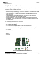
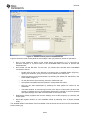
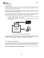
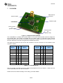
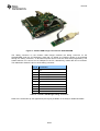
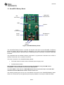
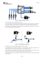
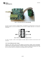
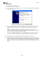
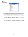
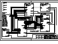
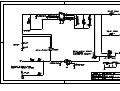
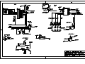
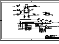
CC2530 ZigBee Development Kit User’s Guide swru209 swru209 Table of contents CC2530 ZIGBEE DEVELOPMENT KIT USER’S GUIDE.......................................................................... 1 1 INTRODUCTION ............................................................................................................................... 3 2 ABOUT THIS MANUAL.................................................................................................................... 3 3 ACRONYMS ....................................................................................................................................... 4 4 ZIGBEE DEVELOPMENT KIT CONTENTS................................................................................... 5 5 GETTING STARTED......................................................................................................................... 7 5.1 SETTING UP THE HARDWARE ................................................................................................................... 7 5.2 RUNNING THE PREPROGRAMMED ZIGBEE SENSOR DEMO ........................................................................ 8 5.3 CC2530 PER TEST ................................................................................................................................. 8 5.4 EVALUATE THE CC2530 RADIO USING SMARTRF STUDIO ....................................................................... 8 5.5 DEVELOPING YOUR OWN SOFTWARE WITH THE CC2530......................................................................... 11 5.6 DEVELOPING YOUR OWN HARDWARE WITH THE CC2530 ....................................................................... 11 6 RF TESTING..................................................................................................................................... 12 6.1 TX PARAMETER TESTING BASICS ......................................................................................................... 12 6.2 RX PARAMETER TESTING BASICS ......................................................................................................... 13 7 CC2530EM ........................................................................................................................................ 14 8 CC2531 USB DONGLE..................................................................................................................... 15 9 SMARTRF05 EVALUATION BOARD............................................................................................ 17 10 SMARTRF05 BATTERY BOARD................................................................................................... 18 10.1 JOYSTICK ............................................................................................................................................. 19 10.2 EM CONNECTORS ................................................................................................................................. 19 10.3 EM SELECTION SWITCH ....................................................................................................................... 20 10.4 PROBE CONNECTORS ............................................................................................................................ 22 10.5 SOC DEBUG CONNECTOR...................................................................................................................... 22 10.6 CURRENT MEASUREMENT JUMPER........................................................................................................ 23 11 FREQUENTLY ASKED QUESTIONS............................................................................................ 24 12 REFERENCES.................................................................................................................................. 26 13 DOCUMENT HISTORY .................................................................................................................. 27 APPENDIX A SCHEMATICS............................................................................................................... 28 2/28 swru209 1 Introduction Thank you for purchasing the CC2530 ZigBee Development Kit. The CC2530 is Texas Instrument’s second generation ZigBee/IEEE 802.15.4 compliant System-onChip with an optimized 8051 MCU core and radio for the 2.4 GHz unlicensed ISM/SRD band. This device enables industrial grade applications by offering state-of-the-art noise immunity, excellent link budget, operation up to 125 degrees and low voltage operation. In addition, the CC2530 provides extensive hardware support for packet handling, data buffering, burst transmissions, data encryption, data authentication, clear channel assessment, link quality indication and packet timing information. Z-Stack™ is TI's ZigBee compliant protocol stack for a growing portfolio of IEEE 802.15.4 products and platforms. Z-Stack support the CC2530 and is compliant with both the ZigBee® 2007 (ZigBee and ZigBee PRO) and ZigBee® 2006 specification. The CC2530 ZigBee Development Kit is well suited for demonstration, evaluation and software development targeting IEEE 802.15.4 and ZigBee compliant applications with the CC2530. The CC2530 product folder on the web [1] has more information, with datasheets, user guides and application notes. For more information about TI’s ZigBee software implementation, refer to the ZStack product folder on the web [4]. This web site also has links for download of Z-stack. 2 About this manual This manual describes all the hardware included in the CC2530 ZigBee Development Kit (CC2530ZDK) and points to other useful information resources. Chapter 4 briefly describes the contents of the development kit and chapter 5 gives a quick introduction to how to get started with the kit. In particular, it describes how to install SmartRF Studio to get the required drivers for the evaluation board, how the hardware can be used, and lists the software that is available for the development kit. Chapter 6 explains some simple methods for performing practical RF testing with the development kit. Chapter 7, 8, and 9 describe the hardware in the kit and where to find more information about how to use it. A troubleshooting guide can be found in chapter 11. The CC2530ZDK Quick Start Guide [6] has a short tutorial on how to get started with this kit. More information and user manuals for the PC tools SmartRF Studio and TI Flash Programmer can be found on their respective product sites on the web [2] [3]. Please visit the CC2530 ZigBee Development Kit [8] web page and CC2530 product page [1] for additional information. Further information can be found on the TI LPRF Online Community [9]. Refer also to the document CC2530DK User’s Guide [5] which gives a detailed description of how to set up the software development environment for the CC2530. This document also lists other available software solutions for CC2530. See chapter 12 for a list of relevant documents and links. 3/28 swru209 3 Acronyms ACM BB CDC DK EB EM HID IC ISM KB LCD LED LPRF MCU NC PER RF RX SoC SPI SRD TI TX UART USB ZDK Z-Stack Abstract Control Model Battery Board Communications Device Class Development Kit Evaluation Board Evaluation Module Human Interface Device Integrated Circuit Industrial, Scientific and Medical Kilo Byte (1024 byte) Liquid Crystal Display Light Emitting Diode Low Power RF Micro Controller Not connected Packet Error Rate Radio Frequency Receive System on Chip Serial Peripheral Interface Short Range Device Texas Instruments Transmit Universal Asynchronous Receive Transmit Universal Serial Bus ZigBee Development Kit TI’s ZigBee software implementation 4/28 swru209 4 ZigBee Development Kit contents The CC2530 ZigBee Development Kit (CC2530DK) includes hardware and software that allows quick testing of the CC2530 RF performance and offers a complete platform for development of advanced prototype RF systems and ZigBee applications. Evaluate the CC2530 and ZigBee right out of the box. The kit can be used to demonstrate a small sensor network application using ZigBee and the CC2530. Use the CC2530ZDK to do software development of your own ZigBee applications using ZStack™ for CC2530. Use SmartRF Studio to perform RF measurements. The radio can be easily configured to measure sensitivity, output power and other RF parameters. Prototype development. All I/O pins from the CC2530 are available on pin connectors on the SmartRF05EB, allowing easy interconnection to peripherals on the EB board or other external sensors and devices. The CC2530ZDK contains the following components 2 x SmartRF05EB (the two large boards) 5 x SmartRF05 Battery Boards 7 x CC2530 Evaluation Modules (with the CC2530 and antenna connector) 1 o 2 of these CC2530EM’s are pre-programmed with the SensorDemo Collector application o 5 of the CC2530EM’s are pre-programmed with the SensorDemo Sensor application 7 x Antennas 1 x CC2531 USB Dongle Cables Batteries Documents Figure 1 - CC2530 ZigBee Development Kit Contents 1 Consult the CC2530ZDK Quick Start Guide [6] and the CC2530ZDK Sensor Demo User’s Guide [7] for a description of the software programmed on the CC2530EM’s. 5/28 swru209 SmartRF05EB The SmartRF05EB (evaluation board) is the main board in the kit with a wide range of user interfaces: 3x16 character serial LCD Full speed USB 2.0 interface UART LEDs Serial Flash Potentiometer Joystick Buttons The EB is the platform for the evaluation modules (EM) and can be connected to the PC via USB to control the EM. CC2530EM The CC2530EM (evaluation module) contains the RF IC and necessary external components and matching filters for getting the most out of the radio. The module can be plugged into the SmartRF05EB. Use the EM as reference design for RF layout. The schematics are included at the end of this document and the layout files can be found on the web [1]. CC2531 USB Dongle The CC2531 USB Dongle is a fully operational USB device that can be plugged into a PC. The dongle has 2 LEDs, two small pushbuttons and connector holes that allow connection of external sensors or devices. The dongle also has a connector for programming and debugging of the CC2531 USB controller. The dongle comes preprogrammed with firmware such that it can be used as a packet sniffer device. SmartRF05BB The SmartRF05 Battery Board can be used as an alternative to the EB, providing a stand alone node when the CC2530EM is connected. It is powered with 2 AA batteries in the sockets underneath the board. The board peripherals include 4 LED’s, 2 push buttons and a joystick. The BB also has a SoC debug connector for connection to an external debug/programming tool e.g. the SmartRF05EB. 6/28 swru209 5 Getting started 5.1 Setting up the hardware After opening the kit, make sure you have all components. Please contact your TI Sales Representative or TI Support [10] if anything is missing. Start by connecting the antennas to the SMA connector on the RF evaluation boards. Tighten the antenna’s screw firmly on to the SMA connector. If not properly connected, you might see reduced RF performance. It is also possible to connect the EM board to RF instruments via coax cables. The EM is designed to match a 50 Ohm load at the SMA connector. Figure 2 CC2530ZDK assembled hardware Next, the evaluation modules should be plugged in to the SmartRF05EB’s and to the SmartRF05BB’s. A ZigBee sensor demo application is preprogrammed on the CC2530EM’s included in this kit. The application consists of two different device types; collectors and sensors. 5 of the CC2530EM’s are programmed as the sensor device type. When running the out of the box demonstration the sensor EM’s shall be connected to the BB’s. The two EM’s programmed as collector device shall be connected to the EB’s. When not using the out of the box demonstration (i.e. the preprogrammed application) e.g, for RF evaluation or software development, all of the 7 EM’s can be used equally. The purpose of the SmartRF05EB is to serve as a general I/O board for testing of the various peripherals of the CC2530 microcontroller. The SmartRF05EB is also used for programming and debugging of the CC2530, and has several useful peripheral devices like LCD, LED’s, I/O connectors, push buttons and joystick etc. The evaluation board can be powered from several different sources: 2 x 1.5V AA batteries (included in this kit) USB (via the USB connector) DC power (4 to 10 Volt) (not included in this kit) 7/28 swru209 External regulated power source (not included in this kit) The power source can be selected using jumper P11 on the SmartRF05EB. The SmartRF05EB User’s Guide [19] provides more details. The SmartRF05 Battery Boards (BB) can be used as a standalone device when equipped with a CC2530EM. This board is powered by AA batteries. See section 10 in this document for more information about the SmartRF05BB. After assembling the hardware, you now have several options for working with the CC2530: 5.2 Run the the sensor demo ZigBee application that is preprogrammed on the CC2530’s. The CC2530ZDK Quick Start Guide document [6] included in this kit describes the necessary steps to run the demonstration. Running the PER test software available for CC2530EM. Chapter 5.3 describes this application. Evaluate and explore the RF capabilities of the CC2530 using SmartRF Studio. Chapter 5.4 provides the details how to do so. Develop your own software for the CC2530. Install IAR Embedded Workbench for 8051 and set up your first software project. Section 5.5 explains how. Develop your own hardware with the CC2530. See chapter 5.6. Running the Preprogrammed ZigBee Sensor Demo The CC2530EM’s are pre-programmed with a Sensor Demo application used to demonstrate a temperature monitoring application in a small ZigBee network. The CC2530ZDK Quick Start Guide document [6] included in this kit describes the necessary steps to run the demonstration. A software package with the source code for the Sensor Demo, and Intel HEX files ready to be programmed on the devices, is available on the CC2530ZDK web site [8]. A detailed description about the Sensor Demo application is found in the document CC2530ZDK Sensor Demo User’s Guide [7]. 5.3 CC2530 PER test A Packet Error Rate (PER) test application is also available for the CC2530. This application can be used to evaluate the RF performance of CC2530 using either the hardware included in the kit or other boards with a CC2530. More information about the PER test application can be found in the documents CC2530DK Quick Start Guide [11] and CC2530 Software Examples User's Guide [12]. A software package with the source code for the PER test application, and Intel HEX files ready to be programmed on the devices, is available on the CC2530DK web site [13]. 5.4 Evaluate the CC2530 Radio using SmartRF Studio SmartRF Studio is a PC application developed for configuration and evaluation of many of the RF-IC products from Texas Instruments, including the CC2530. The application communicates with the CC2530 via the USB controller (the CC2511) on the SmartRF05EB board. The USB controller uses the debug interface of the CC2530 to execute commands and to read and write registers. SmartRF Studio lets you explore the radio on the CC2530, as it gives you full overview and access to the radio registers. The tool has a control interface for running basic radio performance tests from the 8/28 swru209 PC. SmartRF Studio also offers a flexible code export function of radio register settings for software developers. Before proceeding, please download and install the latest version of SmartRF Studio from the web [14]. By installing Studio, the USB drivers needed for proper interaction between the PC and the hardware of the CC2530DK will also be installed. In order to use the SmartRF Studio with CC2530, connect the CC2530EM to the SmartRF05EB. Next, connect the SmartRF05EB board to the PC via one of the USB cables included in the kit. If you have installed SmartRF Studio, select automatic installation of driver in the device wizard that appears. The device wizard will only pop up when you turn on the SmartRF05EB and only once for each board. Allow Windows to complete the driver installation before proceeding. With the board connected to the PC, you can start SmartRF Studio. The following window should appear: Figure 3 - CC2530 and SmartRF Studio Make sure you select the tab called SmartRF® 05 DK. The connected evaluation board should be listed, showing that a CC2530 is available. Actually, all connected SmartRF05EB boards will be listed in this window. The list is dynamically updated as you connect or disconnect a board. Double click on the item showing “CC2530 – new device”, and a new window will appear. 9/28 swru209 Figure 4 - CC2530 control panel in SmartRF Studio Figure 4 shows the main control panel for the CC2530. It lets you perform a number of operations: Run TX Test modes for testing of RF output power and spectrum; e.g. by connecting a spectrum analyser or a power meter to the CC2530EM SMA connector to perform RF measurements. Run Packet TX and RX tests. For this test, you should have two EBs with CC2530EMs connected to the PC. o Double click on both of the devices in the device list in SmartRF Studio (Figure 3), opening two windows, giving control of the two radios at the same time. o Select one device to be the transmitter, by selecting the “Packet TX” tab shown in the lower middle of Figure 4. o On the other device (the receiver), select the “Packet RX” tab. o Set up basic test parameters and press the “Start packet RX” button. o Now you can start transmission by pressing the “Start packet TX” button for the transmitter. o The status window, in the lower right corner of the device control panel, will show the number of packets sent on the transmitter side and the number of received packets and signal strength of the last received packet on the receiver side. Read and/or modify registers and common settings, such as RF frequency (or channel) and output power. Export RF register values in a user modifiable format by selecting “File Export CC2530 Code… ”. The SmartRF Studio User Manual has more details. This document can be found on the Smart Studio product folder [14]. 10/28 swru209 5.5 Developing your own software with the CC2530 To develop software and debug an application on the CC2530, it is recommended to use IAR Embedded Workbench. It supports debugging of CC2530 through the SmartRF05EB, so no additional hardware is required. IAR EW8051 is bundled with all the required files for CC2530 to start development: Register definition header file Linker command file Driver and device description file needed for debugging and programming Note that other compilers and linkers can be used, but these tools may have limited debugging capabilities. An evaluation version of IAR Embedded Workbench is included in the ZigBee Development Kit. To install the software, insert the CD and follow the instructions. You will be asked to register on IAR’s web site to get a license key for the product. As the owner of a CC2530 Development Kit, you are entitled to a 60 day evaluation period. The evaluation version in the kit automatically gives you 30 days. Please contact your local IAR sales representative for the additional 30-days evaluation period. For a list of sales offices and distributors in your country, please see this site: http://www.iar.com/contact. Refer also to the CC2530DK User’s Guide [5] which will guide you through the steps of setting up your own IAR project from scratch. The CC2530DK User’s Guide [5] also gives a brief overview of complete software solutions for CC2530 from Texas Instruments. TI’s ZigBee compliant protocol stack Z-Stack™ can be downloaded from the product folder [4]. This software is needed in order to develop Zigbee application for the CC2530. The product folder include downloads of Z-Stack™ for the various TI platforms. Make sure the version for CC2530 is selected. After installation refer to the Z-stack User’s Guide document found in the installation folders of ZStack™. If Z-Stack™ is installed on the default path the document can be found in the folder C:\Texas Instruments\ZStack-2.2.0-1.3.0\ZStack-CC2530-2.2.0-1.3.0. A software package with the source code for the Sensor Demo, and Intel HEX files ready to be programmed on the devices, is available on the CC2530ZDK web site [8]. This package also includes the CC2530ZDK Sensor Demo User’s Guide giving information about how to set up the software example in the IAR development environment. 5.6 Developing your own hardware with the CC2530 It is recommended to use the CC2530EM as a reference design when designing new hardware using the CC2530. The CC2530EM reference design files can be downloaded from the CC2530 product folder on the web [1]. 11/28 swru209 6 RF Testing NB! When running RF performance tests, it is recommended to disable all other peripherals on the SmartRF05EB in order to avoid unwanted noise on the on-board voltage. In particular, make sure the RS232 level converter/line driver is disabled. RF testing can be performed by using SmartRF Studio together with the Development Kit. The basic set-up is described in section 5.4. As described in that chapter, SmartRF Studio can be used to set up basic tests and tune RF registers accordingly. Since the CC2530 evaluation board is equipped with an SMA connector, both radiated (via antenna) and conducted (via cable) tests can be performed, and it is easy to hook the EM up to RF measurement equipment. The RF equipment may be connected in two different ways. To measure radiated performance, connect an appropriate antenna to the spectrum analyzer or power meter and an antenna on the EM board. To measure conducted performance, connect a 50 Ohm coaxial cable directly from the EM to the RF equipment. Figure 5 - RF Test Set-Up with a Spectrum analyzer By using good-quality RF cabling, the loss in the cabling should be negligible. However make sure that the spectrum analyzer is calibrated. If possible, check it against a calibrated instrument such as an RF signal generator. Uncalibrated spectrum analyzers can display errors of several dBs. 6.1 TX Parameter Testing Basics To investigate the TX performance of the CC2530, you can either use a Spectrum Analyzer or an RF Power Meter. Use the “Simple TX” test mode in SmartRF Studio to set up the device to transmit a signal at the desired frequency. Both a modulated or unmodulated carrier signal can be generated. Use the RF Power Meter to observe the output power or the spectrum analyzer to observe the spectrum and to measure the error vector magnitude (EVM). 12/28 swru209 6.2 RX Parameter Testing Basics To investigate the RX performance of the CC2530, you can use a signal generator or “Packet TX” in SmartRF Studio (with another EB+EM) to generate the packets to receive. The receiver can be configured by using the “Packet RX” test feature in SmartRF Studio. By adding a jammer (a third node that generates either noise on the same channel or a strong signal on an adjacent channel) it is also possible to measure co-channel rejection and selectivity/blocking performance. The PER test application, that was described in section 5.3, can be used for simple sensitivity measurements with the CC2530EM and/or with your own prototype hardware. In this case, connect the unit you want to test to a known good transmitter with coaxial cables and attenuators. Add more attenuators until the PER value is 1%. The signal strength at the receiver side is then the sensitivity limit of the system. For more information regarding sensitivity measurements, refer to “Design Note 2 – Practical Sensitivity Testing” [15]. 13/28 swru209 7 CC2530EM SMA antenna connector 32 kHz Crystal 32MHz Crystal CC2530F256 EM Connector P1 (Bottom side) EM Connector P2 (Bottom side) Figure 6 - CC2530 Evaluation Module The CC2530EM is a complete RF module based on one of the recommended reference designs for the CC2530 radio. The module is equipped with a 32 MHz crystal, a 32.768 kHz crystal, external passive components for the balun and antenna match filter, an SMA connector for the antenna or any other RF instrument connection and general IO headers/connectors. The table below shows the pin-out from the CC2530 to the two connectors on the backside of the evaluation module. CC2530 Signal P1 P1 CC2530 Signal CC2530 Signal P2 P2 CC2530 Signal GND 1 P0.4 3 2 - - 1 2 - 4 P1.3 - 3 4 - P0.1 5 6 P1.0 - 5 6 - P0.2 7 8 - VDD 7 8 - P0.3 9 10 P2.1 VDD 9 10 - P0.0 11 12 P2.2 - 11 12 - P1.1 13 14 P1.4 - 13 14 - P0.6 15 16 P1.5 RESET 15 16 - P0.7 17 18 P1.6 P1.2 17 18 P0.5 GND 19 20 P1.7 P2.0 19 20 - Table 1 - CC2530EM pin-out The part number of the EM connector is SFM-110-02-SM-D-A-K-TR from Samtec. It mates with the TFM-110-02-SM-D-A-K-TR, also from Samtec. Please refer to the reference design on the web [1] for further details. 14/28 swru209 8 CC2531 USB Dongle Meandred F-antenna IO Connector CC2531F256 LEDs Button S2 Button S1 Debug connector Voltage regulator Figure 7 - CC2531 USB Dongle The USB dongle that is included in the kit comes preprogrammed such that it can be used together with the SmartRF Packet Sniffer [16] to capture packets going over the air. To use the dongle as a sniffer, just install the Packet Sniffer PC application (available on the web [16]), plug in the USB dongle and start capturing packets. The Packet Sniffer User Manual [17] has more information. The CC2531 USB dongle can also be used with the Sensor Network Analyzer software from Daintree Networks [18]. The USB dongle can also be used as a general development board for USB and RF software. There is a USB firmware library available from the TI web pages with an implementation of a complete USB framework, including examples showing both HID and CDC ACM. There is a link to this library on the CC2530 DK web pages [13]. Table 2 shows which CC2531 signals are connected to what IO on the dongle. IO Connector CC2531 Dongle User IO CC2531 1 P0.2 Green LED P0.0 2 P0.3 Red LED P1.1 3 P0.4 Button S1 P1.2 4 P0.5 Button S2 P1.3 5 P1.7 6 P1.6 7 P1.5 8 P1.4 Table 2 - CC2531 USB Dongle Pinout In order to debug and program firmware on the CC2531, the CC2531 USB dongle can be connected to the SmartRF05EB as shown in the picture below. The small adapter board and flat cable is included in the development kit. 15/28 swru209 Figure 8 - CC2531 USB Dongle connected to SmartRF05EB The debug connector on the CC2531 USB Dongle matches the debug connector on the SmartRF05EB (and the CC Debugger). Note that, by default, the CC2531 dongle is not powered through the debug connector, so an external power source must be used while programming. The easiest solution is to connect it to a USB port on the PC. Alternatively, resistor R2 can be mounted. The table below shows the pin out of the debug connector. Pin # Connection 1 GND 2 VCC 3 CC2531 P2.2 (DC) 4 CC2531 P2.1 (DD) 5 NC 6 NC 7 CC2531 RESET 8 NC 9 Optional external VCC (R2 must be mounted) 10 NC Table 3 – CC2531 USB Dongle Debug Connector Refer to the schematics (in the appendices) and layout (available on the web) for additional details. 16/28 swru209 9 SmartRF05 Evaluation Board The SmartRF05 Evaluation Board is thoroughly described in the SmartRF05EB User’s Guide [19]. That document will describe the hardware features in detail and provide the schematics for the board. 17/28 swru209 10 SmartRF05 Battery Board 256kB SPI Flash Module EM Connectors LEDs Joystick Probe Connectors EM Selection Switch Power Switch Push Buttons Figure 9 SmartRF05 Battery Board The SmartRF05 Battery Board is a smaller and simpler board than the SmartRF05EB. The Battery Board can together with an EM be used as a standalone node. Figure 9 shows the SmartRF05 Battery Board. The Battery Board is powered with 2 AA batteries placed in the battery connectors underneath the board. The peripherals that are available include 2 push buttons, a joystick with 5 directions and 4 LED’s of different colours that can be controlled via the EM. There are 2 switches on the SmartRF05 Battery Board: The Power switch P6 used to switch the board’s power supply on/off. The EM selection switch. NB: The EM selection switch shall be placed in position SoC/TRX when using a SoC EM such as CC2530EM or a transceiver EM is connected to the Battery Board. The position MSP is used when the CCMSP-EM430F2618 board (not part of this kit) is connected. More information about the EM Selection switch is found in section 10.3. The following sections give the pin out of the different connectors on the SmartRF05 Battery Board. Refer to the schematics (in the appendices) and layout (available on the web) for additional details. 18/28 swru209 10.1 Joystick The joystick detects five positions (centre, up, down, left, right) and one event (pushed). The two aggregated signals, JOY_MOVE and JOY_LEVEL, are used to detect a joystick event when using a SoC (e.g. the CC2530). JOY_MOVE is high whenever the joystick is moved away from the centre position, including pushing. The other signal, JOY_LEVEL, is a voltage level signal that gives different values depending on the current position of the joystick. The table below shows these values. Note that the voltage levels are relative to the voltage on the board. Joystick position JOY_LEVEL (Volts) Up 0.31 Down 1.16 Left 1.62 Right 1.81 Centre 2.12 Table 4 - Voltage on JOY_LEVEL for different joystick positions (T=25°C, Vdd=3.0V) When the EM selection switch is in position MSP, there are 5 discrete signals in addition to JOY_MOVE and JOY_LEVEL, to be used to distinguish which direction the joystick was pressed. These 5 discrete signals are not used with CC2530, only for the CCMSP-EM430F2618 board (not part of this kit).The discrete signals are routed to the EM connectors. See section 10.2 for details. 10.2 EM connectors The EM connectors P1 and P2 are used to connect an EM to the Battery Board. The pin out for these connectors is shown below. Table 1 in section 7 gives information about how the signals of the EM connectors are connected to the CC2530 on the EM board. Note that some of the signals are shared, e.g. IO_LED4_SOC/IO_BUTTON1. This means that the signal is shared between IO’s on the board; in this case both LED 4 when in SoC mode and Button 1. Pressing Button 1 will affect the state of LED 4. Similarly, if a SoC is toggling LED 4, it cannot read from Button 1 at the same time. Function on BB Pin Pin Function on BB GND 1 2 GND Not in use on BB 3 4 FLASH_CS IO_LED4_SOC/IO_BUTTON1 5 6 IO_LED1 Not in use on BB 7 8 JOYSTICK_RT Not in use on BB 9 10 SoC Debug P3.4 Not in use on BB 11 12 SoC Debug P3.3 IO_LED2_SOC 13 14 CS & SoC Debug P3.5 JOY_LEVEL 15 16 SCLK & SoC Debug P3.6 Not in use on BB 17 18 MOSI & SoC Debug P3.8 GND 19 20 MISO & SoC Debug P3.10 Table 5 - EM connector P1 pin-out 19/28 swru209 Function on BB Pin Pin Function on BB JOYSTICK_PUSH 1 2 GND NC 3 4 IO_LED2_MSP Not in use on BB 5 6 IO_LED3_MSP VCC_EM 7 8 IO_LED4_MSP VCC_EM 9 10 NC JOYSTICK_UP 11 12 Not in use on BB JOYSTICK_LEFT 13 14 Not in use on BB SoC Debug P3.7 & Flash Reset 15 16 IO_BUTTON2 Not in use on BB 17 18 Not in use on BB JOY_MOVE 19 20 Not in use on BB Table 6 EM connector P2 pin out 10.3 EM Selection Switch The EM selection switch on SmartRF05BB controls a multiplexer on the board that allows either a connected RF SoC EM or an MSP430 add-on board to access all four LEDs on the evaluation board. The limitation was caused by the particular pin-out on the RF evaluation modules that needed to be backwards compatible with other boards and test equipment. Figure 10 - EM Selection Switch (P8) The switch will both affect the operation of the LEDs and Button 1. NB: The EM Selection switch shall be placed in position SoC/TRX when the CC2530EM is used with SmartRF05BB. 20/28 LED 4 LED 3 LED 2 LED 1 swru209 Figure 11 - Switch P8 effect on LED 1-4 Due to lack of pins, some of the signals are shared. The chip select signal to the EM will also be affected when LED3 is used by the SoC (e.g. CC2530). In most cases, this will not be a problem, since the SoC does not, by default, implement a SPI slave. When LED4 is used by the SoC, the signal from Button 1 might interfere. In short, Button 1 and LED 4 can not be used simultaneously by the SoC. Figure 12 - Switch P8 effect on Button 1 The EM Selection switch will change the polarity of button number 1. In the MSP position, the button is active low, i.e. low voltage when the button is pressed. In the inactive position, the level is high (signal is pulled up by a 10k Ohm resistor). In the SoC position, the button is active high, i.e. high voltage when the button is pressed. In the inactive position, the level is low (signal is pulled down by a 10k Ohm resistor). Note that it is possible to use this feature to determine the position of switch P8 (assuming the button is not pressed). 21/28 swru209 10.4 Probe connectors The probe connectors P4 and P5 bring out all the signals from the EM connectors for probing purposes. The connectors allow easy access to I/O signals and to connect prototyping boards. The pin-out of these connectors are shown below. Function on BB Signal name Pin Pin Signal name Function on BB NC NC 1 2 NC NC Not in use on BB EM_P2_14 3 4 EM_P1_04 FLASH_CS 5 6 EM_P1_13 IO_LED2_SOC 7 8 EM_P1_10 SoC Debug P3.4 9 10 EM_P1_12 SoC Debug P3.3 11 12 13 14 15 16 17 18 19 20 Not in use on BB EM_P2_12 IO_LED4_SOC/IO_BUT TON1 EM_P1_05 Not in use on BB EM_P1_07 Not in use on BB EM_P1_09 Not in use on BB EM_P1_03 Not in use on BB EM_P2_18 Not in use on BB EM_P1_17 Not in use on BB EM_P2_20 EM_P1_20 EM_P1_14 EM_P1_16 EM_P1_18 MISO & SoC Debug P3.10 IO_LED3_SOC & SoC Debug P3.5 SCLK & SoC Debug P3.6 MOSI & SoC Debug P3.8 GND GND Table 7 I/O connector P4 pin out Function on BB Signal name Pin Pin Signal name Function on BB NC NC 1 2 NC NC VCC_EM VCC_EM 3 4 EM_P1_06 IO_LED1 Not in use on BB EM_P2_05 5 6 EM_P2_04 IO_LED2_MSP JOYSTICK_RT EM_P1_08 7 8 EM_P2_06 IO_LED3_MSP JOYSTICK_DN EM_P1_02 9 10 EM_P2_08 IO_LED4_MSP JOYSTICK_UP EM_P2_11 11 12 EM_P1_11 Not in use on BB JOYSTICK_LEFT EM_P2_13 13 14 EM_P2_15 SoC Debug P3.7 & Flash Reset JOYSTICK_PUSH EM_P2_01 15 16 EM_P2_16 IO_BUTTON2 JOY_LEVEL EM_P1_15 17 18 EM_P2_17 Not in use on BB JOY_MOVE EM_P2_19 19 20 GND GND Table 8 I/O connector P5 pin out 10.5 SoC Debug connector The SoC debug connector P3 is used to program and debug the SoC on the connected EM with an external programmer/debug tool. The SmartRF05EB can be used for this purpose by connecting a cable to P3 on the Battery Board as shown in Figure 13 below. 22/28 swru209 Figure 13 Program/debug with SmartRF05EB The pin out of this connector is depicted below. For debugging and programming of the SoC the following signals are used; SoC RESET_N, DD and DC. In addition GND and +3.3V shall be connected. Figure 14 SmartRF05BB SoC Debug Connector As seen on Figure 14 also the SPI signals CS, MISO, MOSI and SCLK can be found on this connector. 10.6 Current Measurement Jumper Jumper P7, also called V_EM, has been added to the board to simplify current consumption measurements. By removing the jumper, an Ampere Meter can easily be connected to the board to perform current consumption measurements. Similarly, a separate, regulated power supply for the EM can be connected. Refer to the schematics (in the appendices) for further details. 23/28 swru209 11 Frequently Asked Questions Q1 When connecting the SmartRF05EB to my PC via USB, the dialog window below appears. Why? What should I do? A1 The SmartRF05EB will be recognized as a USB device by the operating system, and it will ask the user to provide information about which USB driver that should be associated with the device. If you have installed SmartRF Studio, just follow the instructions and select “Automatic installation”. Windows should find the required driver (cebal.sys), as specified in an .inf file. Both files (.inf and .sys) are included in the SmartRF installation. If you have not installed SmartRF Studio, it is recommended that you do so before proceeding. Both the SmartRF Studio User Manual and SmartRF05EB User’s Guide has more details. Q2 SmartRF05EB with the CC2530EM is not detected by IAR/SmartRF Studio. Why? A2 Make sure you have installed SmartRF Studio as described in section 5.4. Then verify that the device is associated with the correct driver by opening the Device Manager on you PC. When the EB is connected, the “Cebal controlled devices” list contains “SmartRF05EB”. If the board is listed as an unknown device, please follow the steps outlined in the SmartRF Studio User Manual. 24/28 swru209 Q3 How can I measure the current consumption of the CC2530? A3 The easiest way to measure current consumption of the chip in various modes is to connect the EM directly to the SmartRF05EB and disconnect everything on the board that consumes power by removing all jumpers. The jumper on header P13 should not be removed. Connect the ampere meter between the two terminals on P15. On P10, the jumper for the EM_RESET signal (connector 35-36) should be mounted. On P1, no jumpers are required, but in order to control the SoC from a debugger, mount a jumper between 19-20 (DBG_DD) and 21-22 (DBG_DD). Make sure the RS232 Enable switch is in the “disable” position. Use SmartRF Studio to set the radio in different modes (RX, TX, etc.), or download an application on the CC2530 setting the device in the preferred state. Q4 Can I use another compiler than IAR to develop software for CC2530? A4 Yes, there are several tools available that can be used for CC2530. Any 8051 compiler (e.g. Keil, GCC, and SDCC) can, in theory, be used. Note that these tools may have limited debugging support for CC2530. 25/28 swru209 12 References [1] CC2530 product web site http://focus.ti.com/docs/prod/folders/print/cc2530.html [2] SmartRF Studio product web site http://focus.ti.com/docs/toolsw/folders/print/smartrftm-studio.html [3] TI Flash Programmer product web site http://focus.ti.com/docs/toolsw/folders/print/flash-programmer.html [4] Z-Stack http://www.ti.com/z-stack [5] CC2530 Development Kit User’s Guide http://www.ti.com/lit/pdf/swru208 [6] CC2530ZDK Quick Start Guide http://www.ti.com/lit/swra274 [7] CC2530ZDK Sensor Demo User’s Guide http://www.ti.com/lit/swru225 [8] CC2530ZDK web site http://focus.ti.com/docs/toolsw/folders/print/cc2530zdk.html [9] Texas Instruments Low Power RF Online Community http://www.ti.com/lprf-forum [10] Texas Instruments Support http://support.ti.com [11] CC2530DK Quick Start Guide http://www.ti.com/lit/swra273 [12] CC2530 Software Examples User’s Guide http://www.ti.com/lit/swru137 [13] CC2530DK web site http://focus.ti.com/docs/toolsw/folders/print/cc2530dk.html [14] SmartRF Studio http://www.ti.com/smartrfstudio [15] DN002 -- Practical Sensitivity Testing http://www.ti.com/lit/swra097 [16] SmartRF Packet Sniffer http://focus.ti.com/docs/toolsw/folders/print/packet-sniffer.html [17]SmartRF Packet Sniffer User Manual http://www.ti.com/lit/swru187 [18]Daintree Networks web site http://www.daintree.net [19]SmartRF05EB User’s Guide http://www.ti.com/lit/swru210 [20] CC2531 product web site http://focus.ti.com/docs/prod/folders/print/cc2531.html 26/28 swru209 13 Document history Revision Date - 2009-06-08 Description/Changes First revision. 27/28 swru209 Appendix A Schematics Please refer to the following pages for the schematics for CC2530 Evaluation Module CC2531 USB Dongle SmartRF05 Evaluation Board The layout for the evaluation module and USB dongle can be found on the CC2530 [1] and CC2531 [20] web pages respectively. 28/28 2 C311 C_100N_0402_X5R_K_10 2 1 C272 C_220P_0402_NP0_J_50 2 1 C271 C_100N_0402_X5R_K_10 2 1 C241 C_100N_0402_X5R_K_10 2 1 C211 C_100N_0402_X5R_K_10 1 C101 C_100N_0402_X5R_K_10 2 C391 C_1U_0402_X5R_K_6P3 1 1 2 FIDUCIAL_MARK FM4 FIDUCIAL_MARK FM2 FIDUCIAL_MARK FM5 FIDUCIAL_MARK FM3 FIDUCIAL_MARK FM6 VDD L1 L_BEAD_102_0402 1 FIDUCIAL_MARK FM1 2 1 2 C1 C_2U2_0402_X5R_M_4VDC CC2530_TX_REDES 1 2 3 P1 SMD_SOCKET_2X10 4 AVDD1 AVDD4 AVDD_GUARD 27 28 18 17 16 15 P0.6 13 P0.7 12 RESET_N 1 32 2 33 C255 C_0402 1 1 C262 C_1P0_0402_NP0_C_50 1 XOSC32M_Q1 XOSC32M_Q2 DCOUPL RBIAS U1 GND 22 23 40 30 41 1 SMD_SOCKET_2X10 P2 1 3 1 2 4 1 C231 C_27P_0402_NP0_J_50 2 4 6 8 10 12 14 16 18 P0.5 20 2 2 P4 PINROW_1x2 1 3 VDD 5 7 9 11 13 Reset 15 P1.2 17 P2.0 19 1 2 P2_3 26 R301 R_56K_0402_F 20 P2_4 2 1 2 1 1 1 2 C_15P_0402_NP0_J_50 C321 37 19 RF_N C253 C_0402 X_32.768/20/50/40/12 X2 38 2 2 3 4 5 L261 L_2N0_0402_S C_15P_0402_NP0_J_50 C331 5 C261 C_18P_0402_NP0_J_50 C221 C_27P_0402_NP0_J_50 6 L251 L_0402 1 7 25 X1 X_32.000/10/15/30/16 8 P1.3 P1.4 P1.5 P1.6 P1.7 P0.0 P0.1 P0.2 P0.3 P0.4 RF_P C401 C_1U_0402_X5R_K_6P3 9 C254 C_2P2_0402_NP0_C_50 1 L252 L_2N0_0402_S C251 C_18P_0402_NP0_J_50 2 11 2 34 1 35 P2_0 P2_1 P2_2 P1_0 P1_1 P1_2 P1_3 P1_4 P1_5 P1_6 P1_7 P0_0 P0_1 P0_2 P0_3 P0_4 P0_5 P0_6 P0_7 2 P2.1 P2.2 P1.0 P1.1 14 1 2 C252 C_1P0_0402_NP0_C_50 31 1 36 P3 SMA_SMD 29 2 P1.3 P1.0 P2.1 P2.2 P1.4 P1.5 P1.6 P1.7 AVDD2 24 1 2 4 6 8 10 12 14 16 18 20 DGND_USB USB_M USB_P DVDD_USB 21 2 P0.4 P0.1 P0.2 P0.3 P0.0 P1.1 P0.6 P0.7 1 3 5 7 9 11 13 15 17 19 DVDD AVDD5/AVDD_SOC AVDD_DREG AVDD3 2 39 1 10 2 CONTRACT NO. 025104 APPROVALS DATE DRAWN TIK NN CHECKED ISSUED COMPANY NAME Texas Instruments DWG CC2530EM Discrete SIZE FSCM NO. DWG NO. A4 SCALE SHEET REV. 1.3.1 1 (1) IMPORTANT NOTICE Texas Instruments Incorporated and its subsidiaries (TI) reserve the right to make corrections, modifications, enhancements, improvements, and other changes to its products and services at any time and to discontinue any product or service without notice. Customers should obtain the latest relevant information before placing orders and should verify that such information is current and complete. All products are sold subject to TI’s terms and conditions of sale supplied at the time of order acknowledgment. TI warrants performance of its hardware products to the specifications applicable at the time of sale in accordance with TI’s standard warranty. Testing and other quality control techniques are used to the extent TI deems necessary to support this warranty. Except where mandated by government requirements, testing of all parameters of each product is not necessarily performed. TI assumes no liability for applications assistance or customer product design. Customers are responsible for their products and applications using TI components. To minimize the risks associated with customer products and applications, customers should provide adequate design and operating safeguards. TI does not warrant or represent that any license, either express or implied, is granted under any TI patent right, copyright, mask work right, or other TI intellectual property right relating to any combination, machine, or process in which TI products or services are used. Information published by TI regarding third-party products or services does not constitute a license from TI to use such products or services or a warranty or endorsement thereof. Use of such information may require a license from a third party under the patents or other intellectual property of the third party, or a license from TI under the patents or other intellectual property of TI. Reproduction of TI information in TI data books or data sheets is permissible only if reproduction is without alteration and is accompanied by all associated warranties, conditions, limitations, and notices. Reproduction of this information with alteration is an unfair and deceptive business practice. TI is not responsible or liable for such altered documentation. Information of third parties may be subject to additional restrictions. Resale of TI products or services with statements different from or beyond the parameters stated by TI for that product or service voids all express and any implied warranties for the associated TI product or service and is an unfair and deceptive business practice. TI is not responsible or liable for any such statements. TI products are not authorized for use in safety-critical applications (such as life support) where a failure of the TI product would reasonably be expected to cause severe personal injury or death, unless officers of the parties have executed an agreement specifically governing such use. Buyers represent that they have all necessary expertise in the safety and regulatory ramifications of their applications, and acknowledge and agree that they are solely responsible for all legal, regulatory and safety-related requirements concerning their products and any use of TI products in such safety-critical applications, notwithstanding any applications-related information or support that may be provided by TI. Further, Buyers must fully indemnify TI and its representatives against any damages arising out of the use of TI products in such safety-critical applications. TI products are neither designed nor intended for use in military/aerospace applications or environments unless the TI products are specifically designated by TI as military-grade or "enhanced plastic." Only products designated by TI as military-grade meet military specifications. Buyers acknowledge and agree that any such use of TI products which TI has not designated as military-grade is solely at the Buyer's risk, and that they are solely responsible for compliance with all legal and regulatory requirements in connection with such use. TI products are neither designed nor intended for use in automotive applications or environments unless the specific TI products are designated by TI as compliant with ISO/TS 16949 requirements. Buyers acknowledge and agree that, if they use any non-designated products in automotive applications, TI will not be responsible for any failure to meet such requirements. Following are URLs where you can obtain information on other Texas Instruments products and application solutions: Products Amplifiers Data Converters DLP® Products DSP Clocks and Timers Interface Logic Power Mgmt Microcontrollers RFID RF/IF and ZigBee® Solutions amplifier.ti.com dataconverter.ti.com www.dlp.com dsp.ti.com www.ti.com/clocks interface.ti.com logic.ti.com power.ti.com microcontroller.ti.com www.ti-rfid.com www.ti.com/lprf Applications Audio Automotive Broadband Digital Control Medical Military Optical Networking Security Telephony Video & Imaging Wireless www.ti.com/audio www.ti.com/automotive www.ti.com/broadband www.ti.com/digitalcontrol www.ti.com/medical www.ti.com/military www.ti.com/opticalnetwork www.ti.com/security www.ti.com/telephony www.ti.com/video www.ti.com/wireless Mailing Address: Texas Instruments, Post Office Box 655303, Dallas, Texas 75265 Copyright © 2009, Texas Instruments Incorporated